JP2019090842A - Display unit device and display device - Google Patents
Display unit device and display device Download PDFInfo
- Publication number
- JP2019090842A JP2019090842A JP2016069894A JP2016069894A JP2019090842A JP 2019090842 A JP2019090842 A JP 2019090842A JP 2016069894 A JP2016069894 A JP 2016069894A JP 2016069894 A JP2016069894 A JP 2016069894A JP 2019090842 A JP2019090842 A JP 2019090842A
- Authority
- JP
- Japan
- Prior art keywords
- light emitting
- circuit board
- display unit
- region
- emitting device
- Prior art date
- Legal status (The legal status is an assumption and is not a legal conclusion. Google has not performed a legal analysis and makes no representation as to the accuracy of the status listed.)
- Pending
Links
- 230000001681 protective effect Effects 0.000 claims abstract description 50
- 238000007789 sealing Methods 0.000 claims description 13
- 239000011347 resin Substances 0.000 description 22
- 229920005989 resin Polymers 0.000 description 22
- 238000010438 heat treatment Methods 0.000 description 7
- 230000002093 peripheral effect Effects 0.000 description 6
- 239000003738 black carbon Substances 0.000 description 5
- 238000000034 method Methods 0.000 description 5
- 230000007423 decrease Effects 0.000 description 4
- 239000000463 material Substances 0.000 description 4
- 229910052751 metal Inorganic materials 0.000 description 4
- 239000002184 metal Substances 0.000 description 4
- 238000002834 transmittance Methods 0.000 description 4
- 230000002238 attenuated effect Effects 0.000 description 3
- 239000003086 colorant Substances 0.000 description 3
- XUIMIQQOPSSXEZ-UHFFFAOYSA-N Silicon Chemical compound [Si] XUIMIQQOPSSXEZ-UHFFFAOYSA-N 0.000 description 2
- 239000012790 adhesive layer Substances 0.000 description 2
- 239000010408 film Substances 0.000 description 2
- 239000010703 silicon Substances 0.000 description 2
- 229910052710 silicon Inorganic materials 0.000 description 2
- 238000005476 soldering Methods 0.000 description 2
- 229920000178 Acrylic resin Polymers 0.000 description 1
- 239000004925 Acrylic resin Substances 0.000 description 1
- RYGMFSIKBFXOCR-UHFFFAOYSA-N Copper Chemical compound [Cu] RYGMFSIKBFXOCR-UHFFFAOYSA-N 0.000 description 1
- OAICVXFJPJFONN-UHFFFAOYSA-N Phosphorus Chemical compound [P] OAICVXFJPJFONN-UHFFFAOYSA-N 0.000 description 1
- 238000010521 absorption reaction Methods 0.000 description 1
- 229910052782 aluminium Inorganic materials 0.000 description 1
- XAGFODPZIPBFFR-UHFFFAOYSA-N aluminium Chemical compound [Al] XAGFODPZIPBFFR-UHFFFAOYSA-N 0.000 description 1
- 239000006229 carbon black Substances 0.000 description 1
- 239000004020 conductor Substances 0.000 description 1
- 229910052802 copper Inorganic materials 0.000 description 1
- 239000010949 copper Substances 0.000 description 1
- 230000003247 decreasing effect Effects 0.000 description 1
- 238000010586 diagram Methods 0.000 description 1
- 239000002270 dispersing agent Substances 0.000 description 1
- 239000000428 dust Substances 0.000 description 1
- 230000001747 exhibiting effect Effects 0.000 description 1
- 238000005286 illumination Methods 0.000 description 1
- 239000010410 layer Substances 0.000 description 1
- 230000035515 penetration Effects 0.000 description 1
- 239000004033 plastic Substances 0.000 description 1
- 229920005668 polycarbonate resin Polymers 0.000 description 1
- 239000004431 polycarbonate resin Substances 0.000 description 1
- 229920001225 polyester resin Polymers 0.000 description 1
- 239000004645 polyester resin Substances 0.000 description 1
- 239000000758 substrate Substances 0.000 description 1
- 239000010409 thin film Substances 0.000 description 1
- 238000011179 visual inspection Methods 0.000 description 1
- XLYOFNOQVPJJNP-UHFFFAOYSA-N water Substances O XLYOFNOQVPJJNP-UHFFFAOYSA-N 0.000 description 1
Images


Classifications
-
- G—PHYSICS
- G09—EDUCATION; CRYPTOGRAPHY; DISPLAY; ADVERTISING; SEALS
- G09F—DISPLAYING; ADVERTISING; SIGNS; LABELS OR NAME-PLATES; SEALS
- G09F9/00—Indicating arrangements for variable information in which the information is built-up on a support by selection or combination of individual elements
- G09F9/30—Indicating arrangements for variable information in which the information is built-up on a support by selection or combination of individual elements in which the desired character or characters are formed by combining individual elements
- G09F9/33—Indicating arrangements for variable information in which the information is built-up on a support by selection or combination of individual elements in which the desired character or characters are formed by combining individual elements being semiconductor devices, e.g. diodes
-
- H—ELECTRICITY
- H01—ELECTRIC ELEMENTS
- H01L—SEMICONDUCTOR DEVICES NOT COVERED BY CLASS H10
- H01L33/00—Semiconductor devices having potential barriers specially adapted for light emission; Processes or apparatus specially adapted for the manufacture or treatment thereof or of parts thereof; Details thereof
Landscapes
- Engineering & Computer Science (AREA)
- Manufacturing & Machinery (AREA)
- Computer Hardware Design (AREA)
- Microelectronics & Electronic Packaging (AREA)
- Power Engineering (AREA)
- Physics & Mathematics (AREA)
- General Physics & Mathematics (AREA)
- Theoretical Computer Science (AREA)
- Devices For Indicating Variable Information By Combining Individual Elements (AREA)
- Led Device Packages (AREA)
Abstract
Description
本発明は、表示ユニット装置及び表示装置に関するものである。 The present invention relates to a display unit device and a display device.
表示装置は、映像を表示するため、屋内、屋外を問わず、様々な場所に設置される。このような表示装置としては、複数の表示ユニット装置をタイル状に配列して表示画面を構成するものが広く用いられている。 Display devices are installed in various places, indoors and outdoors, in order to display an image. As such a display apparatus, what arrange | positions a several display unit apparatus in tile shape, and comprises a display screen is used widely.
表示ユニット装置としては、回路基板に発光装置を複数実装したものが知られている。発光装置としては、凹部を備えるベース部材を有し、この凹部の底面にLED等の発光素子を実装し、この発光素子の周囲を封止部材で封止したものが広く用いられている。このような発光装置は、回路基板に形成された配線に機械的かつ電気的に接続されている。 As a display unit device, a plurality of light emitting devices mounted on a circuit board is known. A light emitting device has a base member provided with a recess, and a light emitting element such as an LED is mounted on the bottom of the recess, and the periphery of the light emitting element is sealed by a sealing member. Such a light emitting device is mechanically and electrically connected to the wiring formed on the circuit board.
従来、このような発光装置のベース部材には、白色樹脂にて形成されたものが用いられてきた(例えば、特許文献1参照)。このため、ベース部材の外周面は、一般に白色を呈する。 Conventionally, as a base member of such a light emitting device, one formed of a white resin has been used (see, for example, Patent Document 1). For this reason, the outer peripheral surface of the base member generally exhibits white.
ところで、表示ユニット装置には、外部に露出した配線等を保護するため、雨水等の浸入を防ぐ保護部が設けられる。例えば、発光装置と、発光装置が実装された回路基板の実装面とを、保護部で一体的に密封するものが知られている(例えば、特許文献2参照)。このような方法によれば、簡易な構成で、発光装置と発光装置が実装された回路基板とを密封することができる。 By the way, in order to protect the wiring etc. which were exposed to the exterior, the display unit apparatus is provided with the protection part which prevents the penetration of rain water etc. FIG. For example, there is known one in which a light emitting device and a mounting surface of a circuit board on which the light emitting device is mounted are integrally sealed by a protective portion (see, for example, Patent Document 2). According to such a method, the light emitting device and the circuit board on which the light emitting device is mounted can be sealed with a simple configuration.
発光装置を構成するベース部材の外周面は白色を呈しているので、太陽光や照明といった周囲光に対する反射率が高く、周囲光の反射や散乱が生じやすい。
また、回路基板に形成された配線は金属部材が外部に露出している。このような金属部材は周囲光に対する反射率が高いため、ベース部材の外周面と同様に、周囲光の反射や散乱が生じやすい。
Since the outer peripheral surface of the base member constituting the light emitting device has a white color, the reflectance to ambient light such as sunlight or illumination is high, and reflection or scattering of ambient light is likely to occur.
Moreover, the metal member has exposed the wiring formed in the circuit board outside. Since such a metal member has a high reflectance to ambient light, reflection and scattering of ambient light are likely to occur, as with the outer peripheral surface of the base member.
特に、発光装置と回路基板の実装面とを保護部で一体的に密封する場合、発光素子からの出射光を効率よく取り出すため、透光性の高い樹脂材料から構成される保護部が使用されることが多い。このような保護部を使用すると、太陽光等の周囲光が、回路基板に形成された配線や、ベース部材の外周面で反射するため、映像のコントラストが低下するという問題がある。 In particular, when the light emitting device and the mounting surface of the circuit board are integrally sealed by a protective portion, a protective portion made of a highly translucent resin material is used in order to efficiently extract the light emitted from the light emitting element. Often. When such a protective portion is used, ambient light such as sunlight is reflected by the wiring formed on the circuit board and the outer peripheral surface of the base member, so that there is a problem that the contrast of the image is lowered.
本発明は上述のような課題を解決するためになされたもので、周囲光の反射を抑制することができる表示ユニット装置、及び表示装置を得ることを目的とする。 The present invention has been made to solve the problems as described above, and it is an object of the present invention to provide a display unit device and a display device capable of suppressing reflection of ambient light.
本発明にかかる表示ユニット装置は、回路基板と、回路基板の実装面に実装された発光装置と、回路基板の実装面と発光装置とを覆うように回路基板に配置される保護部とを備え、保護部は可視光に対して吸収性を備えるものである。 A display unit device according to the present invention includes a circuit board, a light emitting device mounted on the mounting surface of the circuit board, and a protection unit disposed on the circuit board so as to cover the mounting surface of the circuit board and the light emitting device. , And the protective portion is capable of absorbing visible light.
本発明によれば、表示ユニットに周囲光が入射しても、可視光に対する吸収性を備える保護部により吸収され減衰する。このため、周囲光の反射や散乱の発生を抑制することができ、表示ユニット装置に表示される映像のコントラストを向上させることができるようになる。 According to the present invention, even if ambient light is incident on the display unit, the light is absorbed and attenuated by the protective portion having an absorbability to visible light. Therefore, the occurrence of reflection and scattering of ambient light can be suppressed, and the contrast of the image displayed on the display unit device can be improved.
本発明を実施するための形態について添付の図面を参照しながら説明する。なお、各図中、同一又は相当する部分には同一の符号を付しており、その重複説明は適宜に簡略化ないし省略する。また説明の便宜上、各図中に示す部分のサイズ、形状の比例関係等が誇張されている場合がある。 DETAILED DESCRIPTION OF THE INVENTION Embodiments of the present invention will be described with reference to the attached drawings. In the drawings, the same or corresponding parts are denoted by the same reference numerals, and the redundant description will be appropriately simplified or omitted. Further, for the sake of convenience of the description, the proportional relationship between the size and the shape of the portion shown in each drawing may be exaggerated.
実施の形態1.
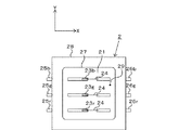
図1〜図5を参照しながら、本発明の実施の形態1にかかる表示ユニット装置1について説明する。図1〜図5では、XYZ座標が規定されている。表示ユニット装置1の正面(表示面)が地面に対して垂直に設置されたと仮定し、左右方向をX軸方向とし、上下方向、すなわち鉛直方向をY軸方向とし、X軸方向及びY軸方向に垂直な方向をZ軸方向として説明する。他の実施の形態においても同様である。
The
図1及び図2に示すように、表示ユニット装置1は、正方形状の平板である回路基板4と、回路基板4の実装面11に実装される複数の発光装置2と、回路基板4の実装面11にX軸方向及びY軸方向に延びるように形成された配線部5と、回路基板4の実装面11と発光装置2とを覆うように配置される保護部3と、配線部5に接続された図示しない駆動IC(Integrated Circuit)とを備える。
As shown in FIGS. 1 and 2, the
発光装置2は、8mm、10mm、16mm等の間隔Dをもって、正方格子状に、回路基板4の実装面11に実装される。実装される発光装置2の個数は、64×64、128×128、256×256、128×256等が代表的である。
The
回路基板4は、絶縁性の樹脂材料等から構成される。配線部5は、銅やアルミ等の金属からなる導電体から構成される。
The
このような表示ユニット装置1では、駆動ICが発光装置2を駆動し、発光装置2から任意の色の可視光が出射することにより、表示ユニット装置1の表示画面に映像が表示される。
In such a
次に、図2〜4を参照しながら発光装置2について詳細に説明する。本実施の形態における発光装置2は、いわゆる3in1型の発光装置であり、赤色光、緑色光、青色光をそれぞれ発光する3つの発光素子23r、23g、23bと、発光素子23r、23g、23bが実装されるパッケージ28と、発光素子23r、23g、23bをパッケージ28内に封止する封止用樹脂27と、発光素子23r、23g、23bと配線部5とをそれぞれ電気的に接続する正極側のリード25r、25g、25b、及び負極側のリード26r、26g、26bとを備える。
Next, the
パッケージ28は、絶縁性の白色樹脂材により構成された筐体であり、上面が開口する凹部29を備える。本実施の形態では、このように凹部29を備えるパッケージ28をベース部材として用いた例について説明する。パッケージ28は、表示ユニット装置1の正面に配置される面を上面とし、回路基板4に直交する面を側面28a、封止用樹脂27が充填される面を内周面28bとする。パッケージ28の凹部29には封止用樹脂27が充填されるため、内周面28bは外部の空間とは接触しないが、パッケージ28の側面28aは外部の空間との接触面を構成する。上述したように、パッケージ28は白色樹脂材により構成されるため、側面28aは白色を呈する。
The
発光素子23r、23g、23bは、いわゆる表面実装型の発光素子であり、パッケージ28に形成された凹部29の底面に、Y軸方向にこの順で、等間隔に配列される。発光素子23r、23g、23bとしては、発光ダイオード(LED:Light Emitting Diode)やレーザダイオード(LD:Laser Diode)等が使用される。
The
これら発光素子23r、23g、23bは、一対の電極を備える。発光素子23r、23g、23bは、リード25r、25g、25bに積載されることにより、一方の電極がリード25r、25g、25bにそれぞれ電気的に接続される。他方の電極は、ワイヤ24によりリード26r、26g、26bに電気的にそれぞれ接続される。リード25r、25g、25b、及びリード26r、26g、26bは、パッケージ28の凹部29の底面においてX軸に沿って夫々側面28aまで延伸し、この側面28aに沿ってパッケージ28の底面まで延伸し、さらに回路基板4の実装面11に沿って屈曲する。
The
回路基板4には、リード25r、25g、25b、及びリード26r、26g、26bを配線部5に対してリフロー方式等を用いた半田付によって接続する接続部6が設けられる。この接続部6により、リード25r、25g、25b、及びリード26r、26g、26bは、回路基板4の実装面11に形成された配線部5に電気的に接続される。
The
封止用樹脂27は、水分や塵埃等から発光素子23r、23g、23b、リード25r、25g、25b、及びリード26r、26g、26bを保護する。封止用樹脂27は、発光素子23r、23g、23bが発光する光に対して透過性を有するシリコン樹脂等によって構成される。
The sealing
封止用樹脂27と外部の空間との接触面は、発光素子23r、23g、23bの発光する光が外部に出射する発光面21を構成する。本実施の形態では、発光面21は、XY平面に平行な平面状に形成されている。
The contact surface between the sealing
このような発光装置2では、駆動ICから配線部5、リード25r、25g、25b及びリード26r、26g、26bを介してそれぞれ独立に供給される電力によって、発光素子23r、23g、23bの発光強度を各別に調整することにより、発光面21から任意の色彩を出射することができる。
In such a
本実施の形態にかかる表示ユニット装置1には、発光装置2と回路基板4の実装面11とを覆う保護部3が配置されている。
保護部3は、回路基板4の実装面11と、発光装置2の発光面21と、パッケージ28の側面28aとに沿って、これら回路基板4の実装面11と、発光装置2の発光面21と、パッケージ28の側面28aとに密着するように構成されている。換言すると、回路基板4に露出する配線部5、接続部6、及び発光装置2は、保護部3により密封されている。さらに、保護部3は、Z軸方向の厚さが、厚さT1となるように構成されている。
In the
The
保護部3は、暗色を呈し、可視光に対する吸収性を備える。また、保護部3は、ポリエステル樹脂、ポリカーボネート樹脂、アクリル樹脂、シリコン樹脂等の防水性を備える樹脂から構成される可撓性を有する薄膜状のフィルムに、カーボンブラック等の黒色の着色剤を添加することにより実現される。可視光に対する吸収率は、着色剤の添加量又は保護部3の厚さT1を変更することで、所望の値に調整することができる。
このような保護部3は、回路基板4に対向する面に粘着層を有し、回路基板4の実装面11、発光装置2の発光面21、及びパッケージ28の側面28aに密着するように構成される。
The
Such a
暗色は、無彩色であっても有彩色であってもよい。視認テストの結果、可視光の透過率が50%以下であることが好ましく、30%以下であることがより好ましい。換言すると、可視光に対する吸収率が50%以上であることが好ましく、70%以上であることがより好ましい。
また、保護部3の厚さT1は、100〜400μmの範囲内にあることが好ましく、150〜300μmの範囲内にあることがより好ましく、190〜210μmの範囲内にあることがより好ましい。
The dark color may be achromatic or chromatic. As a result of the visual inspection, the visible light transmittance is preferably 50% or less, more preferably 30% or less. In other words, the absorptivity for visible light is preferably 50% or more, and more preferably 70% or more.
The thickness T1 of the
図5(a)及び図5(b)に、図1の表示ユニット装置1をB−B線で矢視した断面図を示す。図5(a)は、保護部3として、可視光に対する吸収性を備えないものを用いた場合を示し、図5(b)は、本実施の形態にかかる保護部3を用いた場合を示す。
FIG. 5A and FIG. 5B show cross-sectional views of the
図5(a)に示すように、可視光に対する吸収性を備えない保護部3を使用した場合、表示ユニット装置1に入射した周囲光は、金属が露出する配線部5や、接続部6、及び白色を呈するパッケージ28の側面28aにて反射して外部に出射する。このような反射光は、表示ユニット装置1に表示される映像のコントラスト低下の原因となる。
As shown to Fig.5 (a), when using the
これに対して、本実施の形態にかかる保護部3を使用した場合、図5(b)に示すように、表示ユニット装置1に到達した周囲光は、一部が保護部3に吸収されるため、配線部5、接続部6及びパッケージ28の側面28aに到達する前に減衰する。さらに、配線部5、接続部6及びパッケージ28の側面28aに到達して反射した周囲光も同様に、保護部3に吸収される。このように、本実施の形態にかかる保護部3を使用すると、配線部5、接続部6及びパッケージ28の側面28aにおける反射を抑制し、表示ユニット装置1のコントラストを向上させることができる。
On the other hand, when the
以上のように、本実施の形態では、表示ユニット装置1において、可視光に対する吸収性を備える保護部3を使用するため、表示ユニット装置1に表示される映像のコントラストを向上させることができる。
As described above, in the present embodiment, the
実施の形態2.
実施の形態1では、均一の厚さT1を備える保護部3を用いた場合について説明した。実施の形態2では、保護部3に薄肉部32が形成され場合について説明する。なお、実施の形態1と重複する部分については説明を省略する。
Second Embodiment
In
本実施の形態にかかる保護部3、及び本実施の形態にかかる保護部3を使用した表示ユニット装置1について、図6及び図7を参照しながら詳細に説明する。本実施の形態にかかる保護部3は、凹部31からなる薄肉部32を備える。薄肉部32における保護部3の厚さはTh1であり、薄肉部32以外の厚さTh2及びTh3よりも小さくなるように構成されている。凹部31は、回路基板4と対向する面が開口するように形成される。このような凹部31は、プレス加工といった塑性加工等により、回路基板4において発光装置2が実装される位置に対応するように形成される。
The
保護部3は、図7に示すように、発光装置2の発光面21、回路基板4の実装面11、及びパッケージ28の側面28aに沿って、これら回路基板4の実装面11、パッケージ28の側面28a、及び発光装置2の発光面21に密着するように設けられる。
As shown in FIG. 7, the
ここで、このような本実施の形態にかかる表示ユニット装置1の作成手順について簡単に説明する。
まず、配線部5が形成された回路基板4と、発光装置2とを準備する。
次に、発光装置2のリード25r、25g、25b及びリード26r、26g、26bをリフロー方式等を用いた半田付によって配線部5に接続する。
次に、保護部3を、発光装置2が実装された回路基板4上に、粘着層が回路基板4に対向するとともに薄肉部32が発光装置2の発光面21を覆うように配設する。
Here, a procedure for creating the
First, the
Next, the
Next, the
次に、保護部3と発光装置2が実装された回路基板4とを真空加熱装置に設置し、真空加熱装置内を加熱及び減圧する。減圧により、肉薄部32は発光装置2の発光面21に貼りつく。肉薄部32以外の部位は、加熱により伸長して、発光装置2の側面28a及び回路基板4の実装面11に貼りつく。
最後に、真空加熱装置から表示ユニット装置1を取り出すと、保護部3は大気圧によって押圧され、発光装置2の発光面21、回路基板4の実装面11、及びパッケージ28の側面28aに密着する。
以上の操作によって、表示ユニット装置1を作成できる。
Next, the
Finally, when the
The
発光装置2の発光面21に密着する領域を領域A1、回路基板4の実装面11に密着する領域を領域A2、及びパッケージ28の側面28aに密着する領域を領域A3とする。
The region in close contact with the
上述したように、表示ユニット1の作成時には、薄肉部32が発光装置2の発光面21を覆うように配設される。すなわち、保護部3には、回路基板4において発光装置2が実装される位置に対応して薄肉部32が形成される。このため、領域A1の厚さTh1は、領域A2の厚さTh2及び領域A3の厚さTh3よりも小さくなるように構成される。なお、本実施の形態では領域A2の厚さTh2と領域A3の厚さTh3が等しい構成について説明するが、領域A2の厚さTh2と領域A3の厚さTh3とは異なる厚さとなるように構成してもよい。
As described above, when the
厚さTh1は、10〜100μmの範囲内にあることが好ましく、40〜60μmの範囲内にあることがより好ましい。厚さTh2及び厚さTh3は、100〜400μmの範囲内にあることが好ましく、150〜250μmの範囲内にあることがより好ましい。 The thickness Th1 is preferably in the range of 10 to 100 μm, and more preferably in the range of 40 to 60 μm. The thickness Th2 and the thickness Th3 are preferably in the range of 100 to 400 μm, and more preferably in the range of 150 to 250 μm.
また、領域A2及び領域A3は、可視光に対する透過率が50%以下であることが好ましく、30%以下であることがより好ましい。換言すると、可視光に対する吸収率が50%以上であることが好ましく、70%以上であることがより好ましい。
一方、領域A1は、可視光に対する透過率が70%以上であることが好ましく、80%以上であることがより好ましい。換言すると、可視光に対する吸収率が30%以下であることが好ましく、20%以下であることがより好ましい。
The transmittance of the region A2 and the region A3 to visible light is preferably 50% or less, and more preferably 30% or less. In other words, the absorptivity for visible light is preferably 50% or more, and more preferably 70% or more.
On the other hand, the transmittance of the region A1 to visible light is preferably 70% or more, and more preferably 80% or more. In other words, the absorptivity for visible light is preferably 30% or less, and more preferably 20% or less.
上述したように、発光面21は、可視光に対する吸収性を備える保護部3により覆われているため、発光面21から出射される可視光は、保護部3にて吸収され、減衰してしまう。
As described above, since the
発光面21から出射される可視光が減衰すると、表示ユニット装置1に表示される映像の輝度が低下する。この場合、映像の輝度低下を抑制するため、発光素子23b、23g、23bに供給する電力を増量しなければならなくなる。
When the visible light emitted from the
発光面21から出射される可視光の減衰を抑制する方策として、保護部3の厚さを一様に低減する、又は保護部3に含有されるブラックカーボン量を一様に低下させることで、保護部3の可視光に対する吸収率を一様に低減させることが考えられる。しかしながら、このような方策では、配線部5、接続部6及びパッケージ28の側面28aにおける周囲光の反射を抑制することが困難となってしまう。
As a measure to suppress the attenuation of visible light emitted from the
この点、本実施の形態によれば、発光面21に薄肉部32を形成したため、換言すると、発光面21を覆う領域A1の厚さTh1を領域A2の厚さTh2及び領域A3の厚さTh3よりも小さくなるように構成したため、配線部5、接続部6及びパッケージ28の側面28aにおける周囲光の反射を抑制するとともに、発光面21から出射される可視光の輝度の低下を抑制することができる。
In this respect, according to the present embodiment, the
ところで、樹脂の可視光に対する吸収率Rは、樹脂の吸光係数をα、樹脂の厚さをLとすると、R=1−exp(−αL)で表される。すなわち、樹脂の可視光に対する吸収率Rは、その厚さLが小さくなるにつれて指数関数的に減少する。
上述したように、本実施の形態では、領域A1の厚さTh1について、領域A2の厚さTh2及び領域A3の厚さTh3よりも小さくなるように構成した。このように厚さを調整することで、可視光の透過率を調整したため、領域A2及び領域A3における周囲光の反射を効果的に抑制するとともに、発光面21から出射される可視光の減衰を著しく抑制することができる。
The absorptivity R of the resin to visible light is represented by R = 1−exp (−αL), where α is the absorption coefficient of the resin and L is the thickness of the resin. That is, the absorptivity R to visible light of the resin decreases exponentially as the thickness L decreases.
As described above, in the present embodiment, the thickness Th1 of the area A1 is smaller than the thickness Th2 of the area A2 and the thickness Th3 of the area A3. Since the transmittance of visible light is adjusted by adjusting the thickness in this manner, the reflection of ambient light in the area A2 and the area A3 is effectively suppressed, and the attenuation of the visible light emitted from the
このように、本実施の形態によれば、配線部5、接続部6及びパッケージ28の外周面における可視光の反射を抑制するとともに、発光面21からの出射光22の減衰を著しく抑制することができる。
As described above, according to the present embodiment, the reflection of visible light on the outer peripheral surface of the
実施の形態3.
実施の形態2では、保護部3において、回路基板4と対向する面に凹部31を形成した場合について説明した。実施の形態3では、保護部3において、回路基板4と対向する面と反対側の面に凹部31を形成した場合について説明する。なお、実施の形態1及び2と重複する部分については説明を省略する。
Third Embodiment
In the second embodiment, the case where the
本実施の形態にかかる保護部3、及び本実施の形態にかかる保護部3を使用した表示ユニット装置1について、図8及び図9を参照しながら詳細に説明する。図8及び図9に示すように、本実施の形態では、回路基板4と対向する面と反対側の面に凹部31を形成した。このような保護部3を用いて発光面21を覆うと、発光面21の外周に渡ってZ軸方向に突出する肩部33が形成される。
The
ここで、このような本実施の形態にかかる表示ユニット装置1の作成手順について、実施の形態2と異なる部分を簡単に説明する。実施の形態2と重複する部分については説明を省略する。
本実施の形態では、保護部3を回路基板4に配設する際、発光装置2と対向する面と反対側の面において、凹部31が開口するように配設する。
Here, with respect to the procedure for creating the
In the present embodiment, when the
次に、保護部3と発光装置2が実装された回路基板4とを真空加熱装置に設置し、真空加熱装置内を加熱及び減圧する。この際、肉薄部32以外の部位は、加熱により伸長して、発光装置2の側面28a及び回路基板4の実装面11に貼りつく。この時、保護部3のうち、凹部31の外縁を形成する外縁部31aは、発光装置2の発光面21の外縁に残留し、発光面21の外周を囲う肩部33を形成する。
以上の操作によって、表示ユニット装置1を作成できる。
Next, the
The
このような肩部33が形成されると、太陽光等の周囲光の一部がこの肩部33によって遮られ、発光面21への入射が抑制される。すなわち、肩部33は、庇のような機能を有する。
このように、周囲光の発光面21への入射が抑制されると、発光面21における周囲光の反射が抑制される。これにより、表示ユニット装置1に表示される映像のコントラストを向上させることができるようになる。
When such a
Thus, when the incidence of ambient light on the
本実施の形態によれば、肩部33が発光装置2の発光面21の周囲に形成され、周囲光に対して庇のような働きをするため、より好適に表示ユニット装置1に表示される映像のコントラストを向上させることができる。
According to the present embodiment, the
実施の形態4.
表示装置41は、図8に示すように、タイル状に配置された複数の表示ユニット装置1を備える。表示装置41は、タイル状に配置する表示ユニット装置1の数を増減することにより、任意のサイズの表示画面を構成することができる。
Fourth Embodiment
As shown in FIG. 8, the
表示装置41は、競技場、ビルの壁面等の屋外に設置される。また、体育館等の屋内にも設置できる。表示装置41の表示画面のサイズは、表示装置が設置される、例えば、競技場の広さ、公共空間の大きさ等により、任意に決定される。
The
以上のように、表示ユニット装置1を備えることにより、表示装置41に表示される映像のコントラストを高くすることができる。
As described above, by providing the
ベース部材として、凹部29を備えるパッケージ28を用いたが、ベース部材には、平板状の樹脂成型品を用いることもできる。または、配線パターンがプリントされた素子基板を用いることもできる。
Although the
発光装置2には、1つのパッケージ28に3つの発光ダイオード23r、23g、23bが収容されるいわゆる3in1タイプの発光装置2を用いたが、1つのパッケージ28に発光ダイオード23r、23g、23bのいずれか1つが配置される、いわゆる1in1タイプを用いてもよい。または、4つ以上の発光素子を備えた発光装置2を用いてもよい。封止用樹脂27は、分散剤や蛍光体を含んでいてもよい。
A so-called 3 in 1 type
隣り合う発光装置2の間に、太陽光等の外光の入射を遮るルーバーを設けてもよい。
A louver may be provided between adjacent light emitting
発光面21の形状は、発光面21の中心部分がZ軸方向に最も高くなる凸形状することもできる。また、発光面21の中心部分がZ軸方向に最も低くなる凹形状とすることもできる。
The shape of the
回路基板4の実装面に実装される発光装置2の配置は、正方格子状に限られず、斜方格子、六角格子、矩形格子等の他の格子状でも良い。また、千鳥格子状に配置してもよい。または、一部に発光装置2が配置されないブランクスペースを設けてもよい。
The arrangement of the
保護部3が、薄膜状のフィルムからなる例について説明したが、樹脂成型品としてもよい。
Although the
領域A1に薄肉部32を形成することにより、領域A1における可視光の吸収率を領域A2又は領域A3における可視光の吸収率よりも低くするようにしたが、保護部3の厚さを均等にし、領域A1におけるブラックカーボン含有量を領域A2又は領域A3におけるブラックカーボン含有量よりも少なくすることで、領域A1における可視光の吸収率を、領域A2又は領域A3における可視光の吸収率よりも低くするようにしてもよい。この場合、領域A2におけるブラックカーボン含有量と領域A3におけるブラックカーボン含有量とが異なるようにしてもよい。
By forming the
保護部3は、回路基板4の実装面11、発光装置2の発光面21、及びパッケージ28の側面28aに密着するものとしたが、これらの面に密着していなくてもよい。すなわち、保護部3と回路基板4の実装面との間、保護部3と発光装置2の発光面21との間、及び保護部3とパッケージ28の側面28aとの間には、一部に空気層が設けられていてもよい。
The
本発明は上記実施の形態に限定されるものではなく、その発明の範囲において、各実施の形態を自由に組み合わせたり、各実施の形態を適宜変更、省略したりすることができる。 The present invention is not limited to the above embodiments, and within the scope of the invention, each embodiment can be freely combined, or each embodiment can be appropriately changed or omitted.
1 表示ユニット装置、2 発光装置、3 保護部、4 回路基板、5 配線部、6 接続部、21 発光面、23r、23g、23b 発光素子、24 ワイヤ、25r、25g、25b リード、26r、26g、26b リード、27 封止用樹脂、28 パッケージ、29 凹部、31 凹部、31a 外縁部、32 薄肉部、33 肩部、41 表示装置。
Claims (7)
前記回路基板の実装面に実装された発光装置と、
前記回路基板の実装面と前記発光装置とを覆うように前記回路基板に配置される保護部とを備え、
前記保護部は可視光に対して吸収性を備える
ことを特徴とする表示ユニット装置。 Circuit board,
A light emitting device mounted on the mounting surface of the circuit board;
And a protection unit disposed on the circuit board so as to cover the mounting surface of the circuit board and the light emitting device.
The display unit apparatus, wherein the protection unit has an absorbability to visible light.
前記保護部は、前記封止部と外部の空間との接触面に沿って前記発光装置を覆う第1領域と、前記回路基板の実装面を覆う第2領域と、前記ベース部材と外部の空間との接触面に沿って前記発光装置を覆う、前記第2領域と異なる第3領域を備え、
前記保護部の前記第1領域における可視光に対する吸収率は、前記保護部の前記第2領域における可視光に対する吸収率又は前記保護部の前記第3領域における可視光に対する吸収率よりも小さい
ことを特徴とする請求項1に記載の表示ユニット装置。 The light emitting device includes a base member, a light emitting element mounted on the base member, and a sealing unit for sealing the light emitting element.
The protective portion includes a first region covering the light emitting device along a contact surface between the sealing portion and an external space, a second region covering the mounting surface of the circuit board, and a space between the base member and the external surface. A third area different from the second area, covering the light emitting device along the contact surface with the second area;
The absorptivity for visible light in the first region of the protective portion is smaller than the absorptivity for visible light in the second region of the protective portion or the absorptivity for visible light in the third region of the protective portion. The display unit device according to claim 1, characterized in that:
ことを特徴とする請求項2に記載の表示ユニット装置。 By forming a thin-walled portion having a smaller thickness than the second region or the third region in the first region of the protective portion, the absorptivity for visible light in the first region of the protective portion is protected The display unit device according to claim 2, wherein the absorptivity for visible light in the second area or the third area of the display unit is smaller.
ことを特徴とする請求項3に記載の表示ユニット装置。 The display unit device according to claim 3, wherein the thin portion includes a concave portion formed on a surface facing the circuit board.
ことを特徴とする請求項3に記載の表示ユニット装置。 The display unit device according to claim 3, wherein the thin portion includes a concave portion formed on a surface opposite to the surface facing the circuit board.
ことを特徴とする請求項1〜5のいずれか1項に記載の表示ユニット装置。 The display unit device according to any one of claims 1 to 5, wherein the protective portion is made of a flexible film.
Priority Applications (2)
| Application Number | Priority Date | Filing Date | Title |
|---|---|---|---|
| JP2016069894A JP2019090842A (en) | 2016-03-31 | 2016-03-31 | Display unit device and display device |
| PCT/JP2017/003805 WO2017169092A1 (en) | 2016-03-31 | 2017-02-02 | Display unit and display device |
Applications Claiming Priority (1)
| Application Number | Priority Date | Filing Date | Title |
|---|---|---|---|
| JP2016069894A JP2019090842A (en) | 2016-03-31 | 2016-03-31 | Display unit device and display device |
Publications (1)
| Publication Number | Publication Date |
|---|---|
| JP2019090842A true JP2019090842A (en) | 2019-06-13 |
Family
ID=59963852
Family Applications (1)
| Application Number | Title | Priority Date | Filing Date |
|---|---|---|---|
| JP2016069894A Pending JP2019090842A (en) | 2016-03-31 | 2016-03-31 | Display unit device and display device |
Country Status (2)
| Country | Link |
|---|---|
| JP (1) | JP2019090842A (en) |
| WO (1) | WO2017169092A1 (en) |
Family Cites Families (7)
| Publication number | Priority date | Publication date | Assignee | Title |
|---|---|---|---|---|
| JPH0511714A (en) * | 1991-06-28 | 1993-01-22 | Takiron Co Ltd | Dot matrix light emitting display body and manufacture thereof |
| JPH08129343A (en) * | 1994-11-01 | 1996-05-21 | Hitachi Media Electron:Kk | Matrix display device |
| JP4066620B2 (en) * | 2000-07-21 | 2008-03-26 | 日亜化学工業株式会社 | LIGHT EMITTING ELEMENT, DISPLAY DEVICE HAVING LIGHT EMITTING ELEMENT AND METHOD FOR MANUFACTURING DISPLAY DEVICE |
| JP5092866B2 (en) * | 2008-04-18 | 2012-12-05 | 日亜化学工業株式会社 | Display unit and manufacturing method thereof |
| US9224915B2 (en) * | 2010-09-17 | 2015-12-29 | Rohm Co., Ltd. | Semiconductor light-emitting device, method for producing same, and display device |
| US9882094B2 (en) * | 2011-03-14 | 2018-01-30 | Intellectual Discovery Co., Ltd. | Light source with inner and outer bodies comprising three different encapsulants |
| JP6418812B2 (en) * | 2014-06-30 | 2018-11-07 | 三菱電機株式会社 | Display device |
-
2016
- 2016-03-31 JP JP2016069894A patent/JP2019090842A/en active Pending
-
2017
- 2017-02-02 WO PCT/JP2017/003805 patent/WO2017169092A1/en active Application Filing
Also Published As
| Publication number | Publication date |
|---|---|
| WO2017169092A1 (en) | 2017-10-05 |
Similar Documents
| Publication | Publication Date | Title |
|---|---|---|
| JP6632725B2 (en) | Display device | |
| JP6312586B2 (en) | Display unit, video display apparatus, and display unit manufacturing method | |
| TWI693708B (en) | Transparent display panel | |
| JP6548733B2 (en) | Display unit and method of manufacturing display unit | |
| US10402145B2 (en) | Optoelectronic lighting device, video wall module and signal transmitter for a light signaling installation | |
| TWI578579B (en) | Luminous device, display unit and image display device | |
| JP2017187710A (en) | Display device | |
| JP6846877B2 (en) | Display unit device and display device | |
| JP2019090842A (en) | Display unit device and display device | |
| JP2016213364A (en) | Light-emitting device and display device | |
| JP2020038895A (en) | Light-emitting device | |
| JP2020038778A (en) | Decorating device, method for using light emitting device, and vehicle | |
| JP6599128B2 (en) | Display device | |
| JP4310829B2 (en) | Display device | |
| JP2021071615A (en) | Display device | |
| CN111640847A (en) | LED display device, preparation method thereof and display equipment | |
| US11874547B2 (en) | Film wrapping display | |
| CN212061699U (en) | Prevent blue light LED display screen module | |
| KR20190121692A (en) | Panel and tiled device thereof | |
| CN220821614U (en) | COB display module and display panel | |
| EP4113641A1 (en) | Film wrapping display | |
| CN217482672U (en) | Display module and display device | |
| JP2022081314A (en) | Backlight | |
| JP2020016900A (en) | Display device | |
| JP6495739B2 (en) | Organic EL display panel |