JP2018118477A - Image processing device, control method and program of the same - Google Patents

Image processing device, control method and program of the same Download PDF

Info

Publication number
JP2018118477A
JP2018118477A JP2017012540A JP2017012540A JP2018118477A JP 2018118477 A JP2018118477 A JP 2018118477A JP 2017012540 A JP2017012540 A JP 2017012540A JP 2017012540 A JP2017012540 A JP 2017012540A JP 2018118477 A JP2018118477 A JP 2018118477A
Authority
JP
Japan
Prior art keywords
unit
control unit
processing
image processing
image
Prior art date
Legal status (The legal status is an assumption and is not a legal conclusion. Google has not performed a legal analysis and makes no representation as to the accuracy of the status listed.)
Withdrawn
Application number
JP2017012540A
Other languages
Japanese (ja)
Other versions
JP2018118477A5 (en
Inventor
康智 田中
Yasutomo Tanaka
康智 田中
Current Assignee (The listed assignees may be inaccurate. Google has not performed a legal analysis and makes no representation or warranty as to the accuracy of the list.)
Canon Inc
Original Assignee
Canon Inc
Priority date (The priority date is an assumption and is not a legal conclusion. Google has not performed a legal analysis and makes no representation as to the accuracy of the date listed.)
Filing date
Publication date
Application filed by Canon Inc filed Critical Canon Inc
Priority to JP2017012540A priority Critical patent/JP2018118477A/en
Priority to US15/876,260 priority patent/US20180213103A1/en
Publication of JP2018118477A publication Critical patent/JP2018118477A/en
Publication of JP2018118477A5 publication Critical patent/JP2018118477A5/ja
Withdrawn legal-status Critical Current

Links

Images

Classifications

    • HELECTRICITY
    • H04ELECTRIC COMMUNICATION TECHNIQUE
    • H04NPICTORIAL COMMUNICATION, e.g. TELEVISION
    • H04N1/00Scanning, transmission or reproduction of documents or the like, e.g. facsimile transmission; Details thereof
    • H04N1/00885Power supply means, e.g. arrangements for the control of power supply to the apparatus or components thereof
    • H04N1/00888Control thereof
    • H04N1/00891Switching on or off, e.g. for saving power when not in use
    • GPHYSICS
    • G06COMPUTING; CALCULATING OR COUNTING
    • G06FELECTRIC DIGITAL DATA PROCESSING
    • G06F13/00Interconnection of, or transfer of information or other signals between, memories, input/output devices or central processing units
    • G06F13/14Handling requests for interconnection or transfer
    • G06F13/16Handling requests for interconnection or transfer for access to memory bus
    • G06F13/1668Details of memory controller
    • G06F13/1689Synchronisation and timing concerns
    • HELECTRICITY
    • H04ELECTRIC COMMUNICATION TECHNIQUE
    • H04NPICTORIAL COMMUNICATION, e.g. TELEVISION
    • H04N1/00Scanning, transmission or reproduction of documents or the like, e.g. facsimile transmission; Details thereof
    • H04N1/00002Diagnosis, testing or measuring; Detecting, analysing or monitoring not otherwise provided for
    • H04N1/00026Methods therefor
    • H04N1/00034Measuring, i.e. determining a quantity by comparison with a standard
    • HELECTRICITY
    • H04ELECTRIC COMMUNICATION TECHNIQUE
    • H04NPICTORIAL COMMUNICATION, e.g. TELEVISION
    • H04N1/00Scanning, transmission or reproduction of documents or the like, e.g. facsimile transmission; Details thereof
    • H04N1/00002Diagnosis, testing or measuring; Detecting, analysing or monitoring not otherwise provided for
    • H04N1/00071Diagnosis, testing or measuring; Detecting, analysing or monitoring not otherwise provided for characterised by the action taken
    • H04N1/00082Adjusting or controlling
    • HELECTRICITY
    • H04ELECTRIC COMMUNICATION TECHNIQUE
    • H04NPICTORIAL COMMUNICATION, e.g. TELEVISION
    • H04N1/00Scanning, transmission or reproduction of documents or the like, e.g. facsimile transmission; Details thereof
    • H04N1/00885Power supply means, e.g. arrangements for the control of power supply to the apparatus or components thereof
    • H04N1/00904Arrangements for supplying power to different circuits or for supplying power at different levels
    • HELECTRICITY
    • H04ELECTRIC COMMUNICATION TECHNIQUE
    • H04NPICTORIAL COMMUNICATION, e.g. TELEVISION
    • H04N1/00Scanning, transmission or reproduction of documents or the like, e.g. facsimile transmission; Details thereof
    • H04N1/00912Arrangements for controlling a still picture apparatus or components thereof not otherwise provided for
    • H04N1/00952Using a plurality of control devices, e.g. for different functions
    • HELECTRICITY
    • H04ELECTRIC COMMUNICATION TECHNIQUE
    • H04NPICTORIAL COMMUNICATION, e.g. TELEVISION
    • H04N2201/00Indexing scheme relating to scanning, transmission or reproduction of documents or the like, and to details thereof
    • H04N2201/0077Types of the still picture apparatus
    • H04N2201/0094Multifunctional device, i.e. a device capable of all of reading, reproducing, copying, facsimile transception, file transception
    • YGENERAL TAGGING OF NEW TECHNOLOGICAL DEVELOPMENTS; GENERAL TAGGING OF CROSS-SECTIONAL TECHNOLOGIES SPANNING OVER SEVERAL SECTIONS OF THE IPC; TECHNICAL SUBJECTS COVERED BY FORMER USPC CROSS-REFERENCE ART COLLECTIONS [XRACs] AND DIGESTS
    • Y02TECHNOLOGIES OR APPLICATIONS FOR MITIGATION OR ADAPTATION AGAINST CLIMATE CHANGE
    • Y02DCLIMATE CHANGE MITIGATION TECHNOLOGIES IN INFORMATION AND COMMUNICATION TECHNOLOGIES [ICT], I.E. INFORMATION AND COMMUNICATION TECHNOLOGIES AIMING AT THE REDUCTION OF THEIR OWN ENERGY USE
    • Y02D10/00Energy efficient computing, e.g. low power processors, power management or thermal management

Landscapes

  • Engineering & Computer Science (AREA)
  • Multimedia (AREA)
  • Signal Processing (AREA)
  • Theoretical Computer Science (AREA)
  • Biomedical Technology (AREA)
  • General Health & Medical Sciences (AREA)
  • Health & Medical Sciences (AREA)
  • Physics & Mathematics (AREA)
  • General Engineering & Computer Science (AREA)
  • General Physics & Mathematics (AREA)
  • Facsimiles In General (AREA)
  • Accessory Devices And Overall Control Thereof (AREA)
  • Electrophotography Configuration And Component (AREA)
  • Control Or Security For Electrophotography (AREA)
  • Power Sources (AREA)

Abstract

PROBLEM TO BE SOLVED: To solve a problem in which it is difficult to reduce the entire power consumption including the power consumption of an expansion part if it is determined on whether or not the expansion part is returned to the normal state only by the process number.SOLUTION: An image processing device includes a first control unit having a plurality of processing parts and a second control unit having the plurality of processing parts including the first processing part capable of executing processing common to at least one of the plurality of processing parts. The image processing device measures the memory band performance between the processing part used for execution of the job and a memory when executing the job by using at least one of the plurality of processing parts of the first control unit, makes the first processing part substitutively perform the processing executed by at least one of the plurality of processing parts of the first control unit when the measured memory band performance is larger than a prescribed value, and stops the power supply to the second control unit when the measured memory band performance is equal to or less than the prescribed value.SELECTED DRAWING: Figure 12

Description

本発明は、画像処理装置とその制御方法、及びプログラムに関する。   The present invention relates to an image processing apparatus, a control method thereof, and a program.

スキャナ、プリンタ、コピー、ファクシミリの送受信などの機能を備えたデジタル複合機は、外部装置との間で画像データの入出力動作を制御する制御部と、画像データに対して所定の画像処理を行う複数の画像処理部とを有している。このようなデジタル複合機は様々な顧客に対応するため、低速機から高速機まで幅広く製造されており、それら様々な機器に対応する性能に柔軟に対応できるコントローラが望まれている。そこで、低速機用のコントローラを拡張することで高速機の処理速度に対応できるコントローラ・アーキテクチャがある。機能拡張の例として、例えば低速機用のコントローラに画像処理用のハードウェアを新たに追加することによりメモリ帯域性能を向上させ、より高速な画像処理に対応できるものがある。このような機能拡張が必要な理由として、近年のデジタル複合機ではメモリの集約化が進んでいることが挙げられる。複数の画像処理用のハードウェアが同一のメモリデバイスをワークエリアとして共有するため、そのメモリデバイスのメモリ帯域性能が高速処理のボトルネックになる。従って、高速機では機能拡張により、画像処理用のハードウェアを追加してメモリ帯域性能を向上させている。   A digital multi-function peripheral having functions such as scanner, printer, copy, facsimile transmission / reception and the like performs a predetermined image processing on the image data and a control unit that controls an input / output operation of image data with an external device. A plurality of image processing units. Such digital multi-function peripherals are widely manufactured from low speed machines to high speed machines in order to meet various customers, and a controller that can flexibly cope with performance corresponding to these various devices is desired. Therefore, there is a controller architecture that can cope with the processing speed of high-speed machines by expanding the controller for low-speed machines. As an example of the function expansion, for example, there is one that can improve the memory bandwidth performance by newly adding hardware for image processing to a controller for a low speed machine and can cope with higher speed image processing. One reason why such function expansion is necessary is that memory integration is progressing in recent digital multifunction peripherals. Since multiple image processing hardware shares the same memory device as a work area, the memory bandwidth performance of the memory device becomes a bottleneck for high-speed processing. Therefore, in high-speed machines, memory bandwidth performance is improved by adding hardware for image processing by function expansion.

一方、コントローラを含めたデジタル複合機の消費電力を可能な限り低減することが望まれている。上述した低速機用に用いられるメインのコントローラと高速機用の拡張部を備えた拡張コントローラでは、拡張部を利用しない場合は、その拡張コントローラを省電力状態にすることが望ましい。例えば特許文献1には、メイン側ノードと拡張側ノードにそれぞれCPUを設け、拡張側ノードが未使用のときに拡張側ノード全体を省電力状態とする。そしてメイン側ノードのCPUのプロセス数が増加した場合に拡張側ノードを省電力状態から復帰させることが記載されている。   On the other hand, it is desired to reduce the power consumption of the digital multi-function peripheral including the controller as much as possible. In the extended controller including the main controller used for the low speed machine and the extended section for the high speed machine, when the extended section is not used, it is desirable to put the extended controller in a power saving state. For example, in Patent Document 1, a CPU is provided for each of the main-side node and the expansion-side node, and the entire expansion-side node is put into a power saving state when the expansion-side node is not used. It is described that the expansion side node is returned from the power saving state when the number of processes of the CPU of the main side node increases.

特開2010−211358号公報JP 2010-212358 A

しかしながらCPUのプロセス数に応じて、拡張部を通常状態に復帰させるか否かを判断すると、必要最低限の省電力状態からの復帰とならない場合がある。例えば、メインコントローラのメモリ帯域性能が処理のボトルネックになる場合、例えプロセス数が多くても、必ずしも拡張部を省電力状態から復帰させる必要がない場合がある。なぜなら、メインコントローラによる処理で求められるメモリ帯域は、その処理の種類により異なるため、例えプロセス数が多くでも、必ずしもメモリ帯域性能がネックにならない場合があるためである。このように、メモリの帯域性能が処理のボトルネックになる場合でも、プロセス数のみで拡張部を通常状態に復帰させるか否かを判断すると、拡張部の消費電力を含めた全体の消費電力を低減させることは難しい。   However, if it is determined whether to return the expansion unit to the normal state according to the number of processes of the CPU, there is a case where the return from the minimum power saving state may not be achieved. For example, when the memory bandwidth performance of the main controller becomes a bottleneck for processing, even if the number of processes is large, it is not always necessary to return the expansion unit from the power saving state. This is because the memory bandwidth required for processing by the main controller differs depending on the type of processing, and therefore, even if the number of processes is large, the memory bandwidth performance may not necessarily become a bottleneck. Thus, even when the bandwidth performance of the memory becomes a bottleneck for processing, if it is determined whether or not to return the expansion unit to the normal state only by the number of processes, the total power consumption including the power consumption of the expansion unit is reduced. It is difficult to reduce.

本発明の目的は、上記従来技術の課題を解決することにある。   An object of the present invention is to solve the above-described problems of the prior art.

本発明の目的は、第1の制御部でのメモリ帯域性能に基づいて第2の制御部の処理部による処理の代替の制御、及び第2の制御部への電源供給を制御する技術を提供することにある。   An object of the present invention is to provide a technique for controlling an alternative control of processing by the processing unit of the second control unit and controlling power supply to the second control unit based on the memory bandwidth performance in the first control unit. There is to do.

上記目的を達成するために本発明の一態様に係る画像処理装置は以下のような構成を備える。即ち、
複数の処理部を有する第1の制御部と、
前記複数の処理部と少なくとも一つと共通する処理を実行できる第1処理部を含む複数の処理部を有する第2制御部と、
前記第1及び第2の制御部への電源供給を制御する電源供給手段と、
前記第1の制御部の前記複数の処理部の少なくとも一つを使用してジョブを実行する際、当該ジョブの実行に使用される処理部とメモリとの間のメモリ帯域性能を測定する測定手段と、
前記測定手段により測定された前記メモリ帯域性能が所定値よりも大きい場合は、前記第1の制御部の複数の処理部の少なくとも一つにより実行される処理を、前記第1処理部に代替させ、前記測定手段により測定された前記メモリ帯域性能が所定値以下の場合は、前記電源供給手段により前記第2の制御部への電源供給を停止させるように制御する制御手段と、を有することを特徴とする。
In order to achieve the above object, an image processing apparatus according to an aspect of the present invention has the following arrangement. That is,
A first control unit having a plurality of processing units;
A second control unit having a plurality of processing units including a first processing unit capable of executing processing common to at least one of the plurality of processing units;
Power supply means for controlling power supply to the first and second control units;
Measuring means for measuring memory bandwidth performance between a processing unit and a memory used for execution of the job when executing a job using at least one of the plurality of processing units of the first control unit When,
When the memory bandwidth performance measured by the measuring unit is greater than a predetermined value, the first processing unit is substituted for processing executed by at least one of the plurality of processing units of the first control unit. Control means for controlling the power supply means to stop power supply to the second control unit when the memory bandwidth performance measured by the measurement means is less than or equal to a predetermined value. Features.

本発明によれば、第1の制御部でのメモリ帯域性能に基づいて第2の制御部の処理部による処理の代替制御、及び第2の制御部への電源供給の制御を行うことにより、装置全体の消費電力を、より低減させることができる。   According to the present invention, by performing alternative control of processing by the processing unit of the second control unit and control of power supply to the second control unit based on the memory bandwidth performance in the first control unit, The power consumption of the entire apparatus can be further reduced.

本発明のその他の特徴及び利点は、添付図面を参照とした以下の説明により明らかになるであろう。なお、添付図面においては、同じ若しくは同様の構成には、同じ参照番号を付す。   Other features and advantages of the present invention will become apparent from the following description with reference to the accompanying drawings. In the accompanying drawings, the same or similar components are denoted by the same reference numerals.

添付図面は明細書に含まれ、その一部を構成し、本発明の実施形態を示し、その記述と共に本発明の原理を説明するために用いられる。
本発明の実施形態に係る画像処理装置の一例であるデジタル複合機の構成を説明するブロック図。 本実施形態に係るデジタル複合機のコントローラ部の構成を説明するブロック図。 本実施形態に係るシステム制御部の構成を説明するブロック図。 実施形態に係る複合機のリングバスを流れるパケットデータの構造を説明する図。 実施形態に係るプリント処理部の構成を説明するブロック図(A)、実施形態に係るループバック処理部の構成を説明するブロック図(B)、実施形態に係るスキャン処理部の構成を説明するブロック図(C)。 実施形態に係るループバック処理部のループパック画像処理部の構成を説明するブロック図。 実施形態に係る複合機のリングバススイッチの構成を説明するブロック図。 本実施形態に係る複合機のリングバススイッチによるリングバスの接続制御の一例を説明するブロック図で、拡張コントローラ部を使用しない場合の接続制御を示す。 実施形態に係るリングバススイッチ設定部の構成を説明するブロック図。 実施形態に係る複合機のメインコントローラ部と拡張コントローラ部とが接続されてリングバスを形成する場合の接続制御を説明する図。 実施形態に係る複合機のメインコントローラ部の帯域モニタの構成を説明するブロック図。 実施形態に係る複合機におけるメインコントローラ部と拡張コントローラ部による処理の制御を説明するフローチャート。
The accompanying drawings are included in the specification, constitute a part thereof, show an embodiment of the present invention, and are used together with the description to explain the principle of the present invention.
1 is a block diagram illustrating a configuration of a digital multi-function peripheral that is an example of an image processing apparatus according to an embodiment of the present invention. FIG. 2 is a block diagram illustrating a configuration of a controller unit of the digital multifunction peripheral according to the present embodiment. The block diagram explaining the structure of the system control part which concerns on this embodiment. FIG. 3 is a diagram for explaining the structure of packet data that flows through the ring bus of the multifunction peripheral according to the embodiment. A block diagram for explaining the configuration of the print processing unit according to the embodiment (A), a block diagram for explaining the configuration of the loopback processing unit according to the embodiment (B), and a block for explaining the configuration of the scan processing unit according to the embodiment Figure (C). The block diagram explaining the structure of the loop pack image process part of the loop back process part which concerns on embodiment. FIG. 2 is a block diagram illustrating a configuration of a ring bus switch of the multifunction peripheral according to the embodiment. FIG. 5 is a block diagram for explaining an example of ring bus connection control by a ring bus switch of the multifunction peripheral according to the present embodiment, and shows connection control when an extended controller unit is not used. The block diagram explaining the structure of the ring bus switch setting part which concerns on embodiment. The figure explaining the connection control in case the main controller part and expansion controller part of the multifunctional device which concern on embodiment are connected and a ring bus is formed. FIG. 3 is a block diagram illustrating a configuration of a bandwidth monitor of the main controller unit of the multifunction peripheral according to the embodiment. 6 is a flowchart for explaining processing control by a main controller unit and an expansion controller unit in the multifunction peripheral according to the embodiment.

以下、添付図面を参照して本発明の実施形態を詳しく説明する。尚、以下の実施形態は特許請求の範囲に係る本発明を限定するものでなく、また本実施形態で説明されている特徴の組み合わせの全てが本発明の解決手段に必須のものとは限らない。   Hereinafter, embodiments of the present invention will be described in detail with reference to the accompanying drawings. The following embodiments do not limit the present invention according to the claims, and all combinations of features described in the embodiments are not necessarily essential to the solution means of the present invention. .

図1は、本発明の実施形態に係る画像処理装置の一例であるデジタル複合機100の構成を説明するブロック図である。   FIG. 1 is a block diagram illustrating a configuration of a digital multifunction peripheral 100 that is an example of an image processing apparatus according to an embodiment of the present invention.

スキャナ部110は、原稿を光学的に読み取り、その原稿の画像に対応する画像データを出力する。スキャナ部110は、原稿を光学的に読み取るためのレーザ光源やレンズ等を有する原稿読取部112と、原稿を搬送するベルト等を有する原稿搬送部111とを備えている。プリンタ部140は、記録媒体(用紙)を搬送し、その用紙に画像データに基づく画像を印刷する。プリンタ部140は、用紙を給紙する給紙部142、画像データに基づいて画像を用紙に転写して定着させる転写定着部141、印刷された用紙をソート、ステイプルして機外へ搬出する排紙部143を有している。   The scanner unit 110 optically reads a document and outputs image data corresponding to the image of the document. The scanner unit 110 includes a document reading unit 112 having a laser light source and a lens for optically reading a document, and a document conveying unit 111 having a belt for conveying the document. The printer unit 140 conveys a recording medium (paper) and prints an image based on the image data on the paper. The printer unit 140 includes a paper feeding unit 142 that feeds paper, a transfer fixing unit 141 that transfers and fixes an image on paper based on image data, and a discharge unit that sorts, staples, and transports the printed paper to the outside. A paper portion 143 is provided.

コントローラ部120は、スキャナ部110、プリンタ部140と電気的に接続され、更にLAN,ISDN、インターネット/イントラネット等のネットワーク150と接続されている。ユーザがコピー機能を利用する場合、コントローラ部120は、スキャナ部110を制御して原稿の画像データを取得し、プリンタ部140を制御し、その原稿の画像を用紙に印刷して出力する。またスキャン機能を利用する場合、スキャナ部110を制御して原稿の画像データを取得してコードデータに変換し、ネットワーク150を介してホストPC(不図示)等へ送信する。またプリント機能を利用する場合、ホストPCからネットワーク150を介して受信した印刷データ(コードデータ)を画像データに変換し、プリンタ部140を制御して画像を用紙に印刷して出力する。またISDN等からデータを受信してプリントするファクシミリ(FAX)受信機能や、スキャナ部110から取得した画像データをISDN等へ送信するFAX送信機能も有する。また、これら各機能による処理の実行指示をジョブと呼び、デジタル複合機100は各機能に対応するジョブに従って所定の処理を実行する。操作部130は、ユーザが入力操作を行うためのユーザインタフェースとして機能しており、例えばタッチパネル機能を有する表示部や各種ボタンを含むキーボード等を備えている。   The controller unit 120 is electrically connected to the scanner unit 110 and the printer unit 140, and is further connected to a network 150 such as a LAN, ISDN, Internet / Intranet. When the user uses the copy function, the controller unit 120 controls the scanner unit 110 to acquire document image data, and controls the printer unit 140 to print and output the document image on paper. When the scan function is used, the scanner unit 110 is controlled to acquire document image data, convert it into code data, and transmit it to a host PC (not shown) or the like via the network 150. When the print function is used, print data (code data) received from the host PC via the network 150 is converted into image data, and the printer unit 140 is controlled to print and output the image on paper. Also, a facsimile (FAX) reception function for receiving and printing data from ISDN or the like, and a FAX transmission function for transmitting image data acquired from the scanner unit 110 to ISDN or the like. In addition, the execution instruction of processing by each of these functions is called a job, and the digital multi-function peripheral 100 executes predetermined processing according to the job corresponding to each function. The operation unit 130 functions as a user interface for a user to perform an input operation, and includes a display unit having a touch panel function, a keyboard including various buttons, and the like.

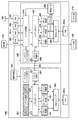
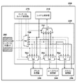
図2は、実施形態に係るデジタル複合機100のコントローラ部120の構成を説明するブロック図である。   FIG. 2 is a block diagram illustrating the configuration of the controller unit 120 of the digital multifunction peripheral 100 according to the embodiment.

コントローラ部120は、リングバス202を介して接続されたメインコントローラ部200と、機能拡張用の拡張コントローラ部201とを有する。更に、ROM290、RAM291a〜291c、HDD(ハードディスクドライブ)292、PHY(Physical Layer)293、電源供給部294を有している。以下、各部について詳しく説明する。尚、実施形態において、メインコントローラ部200及び拡張コントローラ部201はそれぞれ独立したプリント基板等の電子回路基板とする。また拡張コントローラ部201は、ユーザが機能を拡張できるよう着脱可能な構成とする。実施形態では、拡張コントローラ部201の構成をメインコントローラ部200と同一構成としている。但し、機能拡張モジュールとしては、リングバスに接続してパケットデータをやり取り可能なインタフェースを持つものであればどのような機能や構成でもよい。更に、例えば、メインコントローラ部200及び拡張コントローラ部201のそれぞれを、1チップ化したLSIとしてもよい。   The controller unit 120 includes a main controller unit 200 connected via a ring bus 202 and an expansion controller unit 201 for function expansion. Furthermore, it has a ROM 290, RAMs 291a to 291c, an HDD (hard disk drive) 292, a PHY (Physical Layer) 293, and a power supply unit 294. Hereinafter, each part will be described in detail. In the embodiment, the main controller unit 200 and the expansion controller unit 201 are independent electronic circuit boards such as printed boards. The expansion controller unit 201 is configured to be detachable so that the user can expand the function. In the embodiment, the configuration of the extended controller unit 201 is the same as that of the main controller unit 200. However, the function expansion module may have any function or configuration as long as it has an interface that can be connected to the ring bus and exchange packet data. Further, for example, each of the main controller unit 200 and the extended controller unit 201 may be an LSI formed on one chip.

まずメインコントローラ部200について説明する。メインコントローラ部200は、システム制御部210、リングバススイッチ220、プリント処理部230、ループバック処理部240、スキャン処理部250を有する。更に、RAMコントローラ260、リングバススイッチ設定部270、リングバス外部I/F280、帯域モニタ295を有している。   First, the main controller unit 200 will be described. The main controller unit 200 includes a system control unit 210, a ring bus switch 220, a print processing unit 230, a loopback processing unit 240, and a scan processing unit 250. Further, a RAM controller 260, a ring bus switch setting unit 270, a ring bus external I / F 280, and a band monitor 295 are provided.

システム制御部210は、スキャナ部110におけるスキャン処理や、プリンタ部140におけるプリント処理を制御する制御モジュールである。システム制御部210は、リングバススイッチ220とリングバスで接続される。またスキャン処理やプリント処理で用いる画像データの転送制御を、リングバススイッチ220を介して行う。更に、システム制御部210は、ネットワーク150へのデータ送信やネットワーク150からのデータ受信、操作部130への表示処理などシステム全体を統括制御する。   The system control unit 210 is a control module that controls scan processing in the scanner unit 110 and print processing in the printer unit 140. The system control unit 210 is connected to the ring bus switch 220 via a ring bus. Also, transfer control of image data used in scan processing and print processing is performed via the ring bus switch 220. Furthermore, the system control unit 210 performs overall control of the entire system such as data transmission to the network 150, data reception from the network 150, display processing on the operation unit 130, and the like.

リングバススイッチ220は、コントローラ部120内の各モジュールへ画像データを転送するためのリングバスのスイッチ制御を行う。実施形態では、コントローラ部120内の各モジュールへ画像データを転送するためのリングバスが、リングバススイッチ220を介してリング状に繋がっている。これによりシステム制御部210、プリント処理部230、ループバック処理部240、スキャン処理部250、リングバス外部I/F280の間で、画像データのやり取りが可能になっている。リングバススイッチ220の制御は、リングバススイッチ設定部270で行われ、必要に応じてリングバス上の各モジュールの接続先を変更することができる。スイッチ制御の詳細は後述する。   The ring bus switch 220 performs ring bus switch control for transferring image data to each module in the controller unit 120. In the embodiment, a ring bus for transferring image data to each module in the controller unit 120 is connected in a ring shape via the ring bus switch 220. As a result, image data can be exchanged among the system control unit 210, the print processing unit 230, the loopback processing unit 240, the scan processing unit 250, and the ring bus external I / F 280. The ring bus switch 220 is controlled by the ring bus switch setting unit 270, and the connection destination of each module on the ring bus can be changed as necessary. Details of the switch control will be described later.

プリント処理部230は、プリンタ部140で使用する画像データのための色空間変換処理、中間調処理、ガンマ補正処理といったプリント用の画像処理を行う。プリント処理部230は、リングバススイッチ220を介して画像データを受け取り、その画像データに上記プリント用画像処理を施し、処理後の画像データをプリンタ部140へ出力する。   The print processing unit 230 performs image processing for printing such as color space conversion processing, halftone processing, and gamma correction processing for image data used in the printer unit 140. The print processing unit 230 receives the image data via the ring bus switch 220, performs the print image processing on the image data, and outputs the processed image data to the printer unit 140.

ループバック処理部240は、画像データの編集処理を行うブロックで、変倍処理、画像合成処理、回転処理など各種画像処理を実行できる。ループバック処理部240は、システム制御部210からリングバススイッチ220を介して画像データを受け取り、画像処理を施した後、システム制御部210へリングバススイッチ220を介して画像データを戻す。   The loopback processing unit 240 is a block that performs image data editing processing, and can execute various types of image processing such as scaling processing, image composition processing, and rotation processing. The loopback processing unit 240 receives image data from the system control unit 210 via the ring bus switch 220, performs image processing, and then returns the image data to the system control unit 210 via the ring bus switch 220.

スキャン処理部250は、スキャナ部110で取得した画像データに対し、シェーディング補正処理、MTF補正処理、ガンマ補正処理、フィルタ処理といったスキャナ用の画像処理を行う。スキャン処理部250は、スキャナ部110から転送されてきた画像データにスキャナ用の画像処理を施し、処理後の画像データをリングバススイッチ220へ転送する。リングバススイッチ220へ転送された画像データは、リングバスを介してシステム制御部210へ転送される。   The scan processing unit 250 performs image processing for the scanner such as shading correction processing, MTF correction processing, gamma correction processing, and filter processing on the image data acquired by the scanner unit 110. The scan processing unit 250 performs image processing for the scanner on the image data transferred from the scanner unit 110, and transfers the processed image data to the ring bus switch 220. The image data transferred to the ring bus switch 220 is transferred to the system control unit 210 via the ring bus.

RAMコントローラ260は、プリント処理部230、ループバック処理部240、スキャン処理部250から受け取った画像データをRAM291bへ書き込み、RAM291bへ書き込んだ画像データを読み出して転送する処理を行う。プリント処理部230、ループバック処理部240、スキャン処理部250は、それぞれが担当する画像処理を実行するためにRAM291bを一時的な画像バッファとして利用する。このときRAMコントローラ260とRAM291bとの間の転送路には、プリント処理部230、ループバック処理部240、スキャン処理部250それぞれの画像データが多重化して行き交う。そのため、この転送路の処理性能(メモリ帯域性能)を上回るデータ転送が要求されると転送待ち状態が発生する。よって、RAMコントローラ260とRAM291bとの間のデータ転送が、メインコントローラ部200の処理能力のボトルネックとなるケースが多々発生することになる。このメモリ帯域性能はメモリデバイス、メモリコントローラ及び動作周波数により決まるものであり、一般にMB(メガバイト)/s等、単位時間当たりのデータ転送量で表される。RAM291bの使用帯域がメモリデバイスや動作周波数で決まる上限値に達した場合、RAM291bを使用するいずれかの処理が待たされるか、或いは処理が遅くなる。この時、スキャン処理部230やプリント処理部250などのリアルタイム処理が遅くなってしまった場合、システムとして破綻してしまうため、どのような状況においてもリアルタイム処理についてはメモリ帯域の保証が必要となる。   The RAM controller 260 performs processing for writing the image data received from the print processing unit 230, the loopback processing unit 240, and the scan processing unit 250 to the RAM 291b, and reading and transferring the image data written to the RAM 291b. The print processing unit 230, the loopback processing unit 240, and the scan processing unit 250 use the RAM 291b as a temporary image buffer in order to execute the image processing that they are responsible for. At this time, the image data of the print processing unit 230, the loopback processing unit 240, and the scan processing unit 250 are multiplexed and transferred to the transfer path between the RAM controller 260 and the RAM 291b. Therefore, when a data transfer exceeding the processing performance (memory bandwidth performance) of the transfer path is requested, a transfer waiting state occurs. Therefore, there are many cases where data transfer between the RAM controller 260 and the RAM 291b becomes a bottleneck of the processing capability of the main controller unit 200. This memory bandwidth performance is determined by the memory device, the memory controller, and the operating frequency, and is generally represented by a data transfer amount per unit time such as MB (megabyte) / s. When the use band of the RAM 291b reaches the upper limit value determined by the memory device and the operating frequency, any process using the RAM 291b is waited or the process is delayed. At this time, if the real-time processing of the scan processing unit 230, the print processing unit 250, or the like is delayed, the system will fail, and in any situation, it is necessary to guarantee the memory bandwidth for the real-time processing. .

バス帯域モニタ295は、メインコントローラ部200におけるRAM291bのメモリ帯域性能を測定する。帯域モニタ295は、メインコントローラ部200のプリント処理部230、ループバック処理部240、スキャン処理部250の各処理部とRAMコントローラ260との間に接続され、RAM291bの使用帯域性能をモニタする。帯域モニタ295の詳細については図11を参照して後述する。   The bus bandwidth monitor 295 measures the memory bandwidth performance of the RAM 291b in the main controller unit 200. The bandwidth monitor 295 is connected between the print processing unit 230, the loopback processing unit 240, and the scan processing unit 250 of the main controller unit 200 and the RAM controller 260, and monitors the used bandwidth performance of the RAM 291b. Details of the bandwidth monitor 295 will be described later with reference to FIG.

リングバス外部I/F280は、リングバススイッチ220を介してメインコントローラ部200と外部とを接続し、外部との間でパケットデータの入出力を行う。このリングバス外部I/F280を介して、メインコントローラ部200と拡張コントローラ部201との間でデータ転送が行われる。つまり実施形態では、拡張コントローラ部201がリングバス外部I/F280を介してメインコントローラ部200と接続され、1個のリングバス202を形成している。   The ring bus external I / F 280 connects the main controller unit 200 and the outside via the ring bus switch 220 and inputs / outputs packet data to / from the outside. Data transfer is performed between the main controller unit 200 and the expansion controller unit 201 via the ring bus external I / F 280. That is, in the embodiment, the extended controller unit 201 is connected to the main controller unit 200 via the ring bus external I / F 280 to form one ring bus 202.

次に、拡張コントローラ部201について説明する。この拡張コントローラ部201は、コントローラ部120の処理を高速化するための機能拡張モジュールである。実施形態では、拡張コントローラ部201は、デジタル複合機100のメモリ帯域性能を増加させる目的で使用される。上述したようにメインコントローラ部200のRAM291bのメモリ帯域性能は、使用するメモリデバイス及び、動作周波数により決定されるため限界がある。高速機においては、中低速機に比べ高速に画像処理を行う必要があるため、メインコントローラ部200と拡張コントローラ部201の2つを使用することにより、画像処理システムとしてのメモリ帯域性能を向上させることができる。   Next, the extended controller unit 201 will be described. The expansion controller unit 201 is a function expansion module for speeding up the processing of the controller unit 120. In the embodiment, the extended controller unit 201 is used for the purpose of increasing the memory bandwidth performance of the digital multi-function peripheral 100. As described above, the memory bandwidth performance of the RAM 291b of the main controller unit 200 is limited because it is determined by the memory device to be used and the operating frequency. Since high-speed machines need to perform image processing at a higher speed than medium- and low-speed machines, the memory bandwidth performance as an image processing system is improved by using two of the main controller unit 200 and the extended controller unit 201. be able to.

実施形態では、拡張コントローラ部201の構成とメインコントローラ部200の構成が同一である。即ち、拡張コントローラ部201は、システム制御部211、リングバススイッチ221、プリント処理部231、ループバック処理部241、スキャン処理部251を有している。更に、拡張コントローラ部201は、RAMコントローラ261、リングバススイッチ設定部271、リングバス外部I/F281を有している。これら各部の機能は、メインコントローラ部200内の対応する各部の機能と同じである。このような構成を採用することで、メインコントローラ部200とは別に拡張コントローラ部201を設計する開発コストを抑えることができる。尚、実施形態では、拡張コントローラ部201のプリント処理部231、ループバック処理部241、スキャン処理部251の内、実際に拡張機能として使用されるのはループバック処理部241である。これはプリント処理部231やスキャン処理部251を使用すると、プリンタ部140、スキャナ部110の接続をメインコントローラ部200から拡張コントローラ部201へ変更する必要が発生し、コントローラ部120の構成が複雑化するためである。図2において、拡張コントローラ部201のシステム制御部211、プリント処理部231、スキャン処理部251はグレーアウトし、動作させる必要のないことを示している。図2においてグレーアウトされた部分は、クロック信号の供給が停止された省電力状態としてもよい。   In the embodiment, the configuration of the extension controller unit 201 and the configuration of the main controller unit 200 are the same. That is, the extended controller unit 201 includes a system control unit 211, a ring bus switch 221, a print processing unit 231, a loopback processing unit 241, and a scan processing unit 251. Further, the expansion controller unit 201 includes a RAM controller 261, a ring bus switch setting unit 271, and a ring bus external I / F 281. The functions of these units are the same as the functions of the corresponding units in the main controller unit 200. By adopting such a configuration, the development cost for designing the extended controller unit 201 separately from the main controller unit 200 can be suppressed. In the embodiment, among the print processing unit 231, the loopback processing unit 241, and the scan processing unit 251 of the extended controller unit 201, the loopback processing unit 241 is actually used as an extended function. When the print processing unit 231 or the scan processing unit 251 is used, it is necessary to change the connection of the printer unit 140 and the scanner unit 110 from the main controller unit 200 to the extended controller unit 201, and the configuration of the controller unit 120 becomes complicated. It is to do. In FIG. 2, the system control unit 211, the print processing unit 231, and the scan processing unit 251 of the extended controller unit 201 are grayed out, indicating that it is not necessary to operate them. 2 may be in a power saving state in which the supply of the clock signal is stopped.

電源供給部294は、メインコントローラ部200と拡張コントローラ部201への電源供給を制御する。複合機100の電源がオンされると、電源供給部294はコントローラ部120内部でメインコントローラ部200のみに電源供給を開始する。拡張コントローラ部201への電源供給は、メインコントローラ部200のシステム制御部210からの指示に従って制御される。よって、システム制御部210からの電源供給の指示があった場合にのみ拡張コントローラ部201へ電源供給を行い、電源供給の停止指示があった場合には電源供給を停止させる。   The power supply unit 294 controls power supply to the main controller unit 200 and the expansion controller unit 201. When the multifunction device 100 is turned on, the power supply unit 294 starts supplying power only to the main controller unit 200 inside the controller unit 120. Power supply to the extension controller unit 201 is controlled in accordance with an instruction from the system control unit 210 of the main controller unit 200. Therefore, power is supplied to the expansion controller unit 201 only when there is a power supply instruction from the system control unit 210, and power supply is stopped when there is a power supply stop instruction.

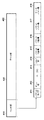
図3は、実施形態に係るシステム制御部210の構成を説明するブロック図である。以下、システム制御部210を構成する各要素について説明する。尚、拡張コントローラ部201のシステム制御部211も同様の構成である。   FIG. 3 is a block diagram illustrating the configuration of the system control unit 210 according to the embodiment. Hereinafter, each element constituting the system control unit 210 will be described. The system control unit 211 of the extended controller unit 201 has the same configuration.

CPU310は、複合機100全体を制御するプロセッサである。CPU310は、RAM291aに展開されたOS(オペレーティングシステム)や制御プログラムに従って、プリント処理やスキャン処理といったジョブ処理を統括的に制御する。ROMコントローラ320は、ブートプラグラムを格納しているROM290にアクセスするための制御モジュールである。デジタル複合機100の電源がオンされるとCPU310は、ROMコントローラ320を介してROM290にアクセスしてブートプログラムを実行し、HDD292からRAM291aにプログラムを展開する。RAMコントローラ330は、制御プログラムや画像データを格納するRAM291aにアクセスするための制御モジュールである。RAMコントローラ330は、RAM291aの設定や制御を行うためのレジスタを備えており、このレジスタは、CPU310からアクセス可能である。操作部インタフェース340は、ユーザによる操作部130を介した操作指示の受付、及び操作結果の表示等を制御する。HDD292は、システムソフトウェアやアプリケーションプログラム、画像データと各画像データに対応するページ情報やジョブ情報を格納する。HDD292は、HDDコントローラ360を介してシステムバス300に接続されており、CPU310の指示に従ってデータの書き込みや読み出しを行う。LANコントローラ370はPHY293を介してネットワーク150に接続し、外部のホストコンピュータとの間で画像データなどの情報の入出力を行う。モデム372は図示しない公衆回線に接続され、FAX送信やFAX受信ジョブを処理する際に外部のFAX機器とデータ通信を行う。   The CPU 310 is a processor that controls the entire multifunction peripheral 100. The CPU 310 comprehensively controls job processing such as print processing and scan processing in accordance with an OS (operating system) and control program developed in the RAM 291a. The ROM controller 320 is a control module for accessing the ROM 290 storing the boot program. When the power of the digital multi-function peripheral 100 is turned on, the CPU 310 accesses the ROM 290 via the ROM controller 320 to execute the boot program, and expands the program from the HDD 292 to the RAM 291a. The RAM controller 330 is a control module for accessing a RAM 291a that stores a control program and image data. The RAM controller 330 includes a register for setting and controlling the RAM 291a, and this register is accessible from the CPU 310. The operation unit interface 340 controls reception of an operation instruction by the user via the operation unit 130, display of an operation result, and the like. The HDD 292 stores system software, application programs, image data, and page information and job information corresponding to each image data. The HDD 292 is connected to the system bus 300 via the HDD controller 360 and writes and reads data according to instructions from the CPU 310. The LAN controller 370 is connected to the network 150 via the PHY 293 and inputs / outputs information such as image data to / from an external host computer. The modem 372 is connected to a public line (not shown), and performs data communication with an external FAX device when processing a FAX transmission or FAX reception job.

画像圧縮部350は、RAM291a又はHDD292に格納される画像データを、例えばJPEGフォーマットに圧縮処理する。また画像伸張部351は、例えばJPEGフォーマットに圧縮された画像データを伸張する。レンダリング部352は、ネットワーク150からLANコントローラ370を経由して受信した画像データ(PDLデータ)を、プリンタ部140で取り扱い可能なビットマップデータに変換する。   The image compression unit 350 compresses image data stored in the RAM 291a or the HDD 292 into, for example, a JPEG format. The image decompression unit 351 decompresses image data compressed in, for example, the JPEG format. The rendering unit 352 converts image data (PDL data) received from the network 150 via the LAN controller 370 into bitmap data that can be handled by the printer unit 140.

電源制御部380は、メインコントローラ部200の各ブロックに対して、未使用ブロックへのクロック供給を止めるなどの省電力制御を行う。例えば、省電力では、拡張コントローラ201のシステム制御部211の電源制御部は、システム制御部211やプリント処理部231、スキャン処理部251といった未使用ブロックへのクロック信号の供給を停止している。   The power supply control unit 380 performs power saving control such as stopping clock supply to unused blocks for each block of the main controller unit 200. For example, in power saving, the power control unit of the system control unit 211 of the expansion controller 201 stops supplying clock signals to unused blocks such as the system control unit 211, the print processing unit 231, and the scan processing unit 251.

GPIO制御部390は、コントローラ部120に備えられているGPIO(汎用IOポート)を制御するブロックである。このブロックはCPU310によって制御され、GPIOの状態を制御する。本実施形態では、GPIO制御部390から出力されるGPIO信号はシステム制御部210の外部へ出力され、コントローラ部120の電源供給部294へ接続されている。電源供給部294は、このGPIO信号がロウレベルの状態のとき拡張コントローラ201への電源供給を停止し、ハイレベルのときに拡張コントローラ201へ電源を供給する。これによりCPU310は、拡張コントローラ201への電源供給を制御することができる。尚、このGPIO信号の初期状態はロウレベルである。   The GPIO control unit 390 is a block that controls a GPIO (general-purpose IO port) provided in the controller unit 120. This block is controlled by the CPU 310 to control the state of GPIO. In the present embodiment, the GPIO signal output from the GPIO control unit 390 is output to the outside of the system control unit 210 and is connected to the power supply unit 294 of the controller unit 120. The power supply unit 294 stops the power supply to the expansion controller 201 when the GPIO signal is in a low level, and supplies the power to the expansion controller 201 when the GPIO signal is at a high level. As a result, the CPU 310 can control power supply to the expansion controller 201. Note that the initial state of the GPIO signal is at a low level.

リングバスインタフェース301は、システム制御部210のシステムバス300と、システム制御部210外のリングバススイッチ220を中心としたリングバスとを接続するインタフェースである。リングバスを流れるデータをパケットデータと呼び、リングバスインタフェース301は、RAM291a又はHDD292に格納されたパケットデータをリングバスへ送信する。また、リングバスから受信したパケットデータをRAM291a又はHDD292に格納する。   The ring bus interface 301 is an interface that connects the system bus 300 of the system control unit 210 and a ring bus centering on the ring bus switch 220 outside the system control unit 210. Data flowing through the ring bus is referred to as packet data, and the ring bus interface 301 transmits the packet data stored in the RAM 291a or the HDD 292 to the ring bus. The packet data received from the ring bus is stored in the RAM 291a or the HDD 292.

次にパケットデータについて説明する。   Next, packet data will be described.

図4は、実施形態に係る複合機100のリングバスを流れるパケットデータの構造を説明する図である。   FIG. 4 is a diagram illustrating the structure of packet data that flows through the ring bus of the multifunction peripheral 100 according to the embodiment.

パケットデータ400は、ヘッダ部410とデータ部420とを含んでいる。ヘッダ部410は更に、パケットタイプ411、チップID412、ページID413、ジョブID414、パケットY座標、パケットX座標、パケットバイト長、データバイト長418を含んでいる。   The packet data 400 includes a header part 410 and a data part 420. The header section 410 further includes a packet type 411, a chip ID 412, a page ID 413, a job ID 414, a packet Y coordinate, a packet X coordinate, a packet byte length, and a data byte length 418.

パケットタイプ411は、そのパケットが画像データか、コマンドなのかを示す。パケットタイプ411が画像データを示す場合には、データ部420には画像データが格納されている。一方、パケットタイプ411がコマンドを示す場合は、データ部420には各画像処理部の係数やモードなどを設定するための設定アドレスと設定値が格納されている。チップID412は、このパケットを送信するターゲットとなる処理部を識別するためのID(識別子)である。例えば、ID「0」はプリント処理部230、ID「1」はループバック処理部240、ID「2」はスキャン処理部250、ID「3」は拡張コントローラ201内のループバック処理部241等である。ページID413は、このパケットが属するページ番号を示す。スキャンやプリントといった処理は複数ページ実施される場合があり、その場合に、何ページ目に属するパケットかを示す。ジョブID414は、このパケットの属するジョブ番号を示している。例えば、スキャンジョブとプリントジョブが同時に実施される場合は、スキャンジョブのパケットには「ジョブ番号1」、プリントジョブのパケットには「ジョブ番号2」というように、ジョブ番号が付与され、これにより各ジョブを識別することできる。パケットY座標415は、データ部420に画像データが格納されている場合、その画像データがページ内のどのY座標に位置するかを示す。またパケットX座標416は、データ部420に画像データが格納されている場合、その画像データがページ内のどのX座標に位置するかを示す。データ部420に格納される画像データは、ページ単位の画像データを、所定の画素数(例えば、32画素×32画素)の矩形サイズに分割したものである。よって、パケットデータからページデータを再生成する場合に、これらX,Y座標が参照される。尚、この画像データは画像圧縮部350又は各画像処理部の内部に実装されている圧縮器によって圧縮されており、圧縮画像データとしてデータ部420に格納されている。パケットバイト長417は、このパケットのトータルバイト数を示し、データバイト長418はデータ部420のトータルバイト数を示す。   The packet type 411 indicates whether the packet is image data or a command. When the packet type 411 indicates image data, the data portion 420 stores image data. On the other hand, when the packet type 411 indicates a command, the data unit 420 stores a setting address and a setting value for setting the coefficient, mode, and the like of each image processing unit. The chip ID 412 is an ID (identifier) for identifying a processing unit that is a target for transmitting the packet. For example, ID “0” is the print processing unit 230, ID “1” is the loopback processing unit 240, ID “2” is the scan processing unit 250, ID “3” is the loopback processing unit 241 in the expansion controller 201, and the like. is there. The page ID 413 indicates the page number to which this packet belongs. A process such as scanning or printing may be performed for a plurality of pages, and in this case, it indicates what page the packet belongs to. The job ID 414 indicates the job number to which this packet belongs. For example, when a scan job and a print job are executed at the same time, a job number such as “job number 1” is assigned to the scan job packet and “job number 2” is assigned to the print job packet. Each job can be identified. The packet Y coordinate 415 indicates the Y coordinate in the page when the image data is stored in the data unit 420. The packet X coordinate 416 indicates where the image data is located in the page when the image data is stored in the data unit 420. The image data stored in the data unit 420 is obtained by dividing page-unit image data into rectangular sizes of a predetermined number of pixels (for example, 32 pixels × 32 pixels). Therefore, when the page data is regenerated from the packet data, these X and Y coordinates are referred to. The image data is compressed by the image compression unit 350 or a compressor mounted inside each image processing unit, and stored in the data unit 420 as compressed image data. The packet byte length 417 indicates the total number of bytes of the packet, and the data byte length 418 indicates the total number of bytes of the data portion 420.

以上説明したようなパケットデータがリングバス上を流れる。各画像処理部はパケットデータを受信、解釈し、コマンドを示すパケットであれば処理のモードや係数などを設定し、画像データを示すパケットであれば画像データに画像処理を実施する。   Packet data as described above flows on the ring bus. Each image processing unit receives and interprets packet data, and if the packet indicates a command, sets a processing mode, a coefficient, and the like. If the packet indicates image data, the image processing unit performs image processing on the image data.

次に、実施形態に係るプリント処理部230、ループバック処理部240、スキャン処理部250について、図5を参照して詳しく説明する。   Next, the print processing unit 230, the loopback processing unit 240, and the scan processing unit 250 according to the embodiment will be described in detail with reference to FIG.

図5(A)は、実施形態に係るプリント処理部230の構成を説明するブロック図である。   FIG. 5A is a block diagram illustrating the configuration of the print processing unit 230 according to the embodiment.

リングバスインタフェース(I/F)500は、プリント処理部230内の各部と、プリント処理部230の外のリングバススイッチ220を中心としたリングバスとを接続するインタフェースである。リングバスインタフェース500は、パケット入力部501とパケット出力部502とを有している。パケットデータを受信すると、パケット入力部501はヘッダ部410のチップID412を参照し、パケット入力部501に割り振られたチップIDと同一かどうかをチェックする。チップID412の示すIDが、そのパケット入力部501に割り振られたチップIDと異なる場合、処理すべきパケットデータではないと判断して、そのパケットデータをパケット出力部502に転送する。   A ring bus interface (I / F) 500 is an interface that connects each unit in the print processing unit 230 and a ring bus centering on the ring bus switch 220 outside the print processing unit 230. The ring bus interface 500 includes a packet input unit 501 and a packet output unit 502. When the packet data is received, the packet input unit 501 refers to the chip ID 412 of the header unit 410 and checks whether the chip ID assigned to the packet input unit 501 is the same. If the ID indicated by the chip ID 412 is different from the chip ID assigned to the packet input unit 501, it is determined that the packet data is not to be processed, and the packet data is transferred to the packet output unit 502.

一方、チップID412の示すIDが、そのパケット入力部501に割り振られたチップIDと同一である場合、そのパケットが画像データであれば内部の画像処理パス(伸張器503〜プリンタ画像処理部505)を通して画像処理を実行する。またそのパケットがコマンドであれば、データ部420に格納されている設定アドレスと設定値とを参照し、指定された画像処理部の係数やモードを設定保持部506に設定する。またそのパケットが設定値をリードするコマンドであれば、設定保持部506は、設定値を格納したパケットデータをリングバスインタフェース500に送る。伸張器503、パケットラスタ変換部504及びプリンタ画像処理部505は、設定保持部506に保持された設定値に基づいて処理を行う。   On the other hand, when the ID indicated by the chip ID 412 is the same as the chip ID assigned to the packet input unit 501, if the packet is image data, an internal image processing path (decompressor 503 to printer image processing unit 505). To perform image processing. If the packet is a command, the setting address and setting value stored in the data unit 420 are referred to, and the coefficient and mode of the designated image processing unit are set in the setting holding unit 506. If the packet is a command for reading a setting value, the setting holding unit 506 sends packet data storing the setting value to the ring bus interface 500. The decompressor 503, the packet raster conversion unit 504, and the printer image processing unit 505 perform processing based on the setting value held in the setting holding unit 506.

パケット出力部502は、パケット入力部501から転送されるパケットデータ、及び設定保持部506からのパケットデータの調停を行って、リングバスにパケットデータを転送する。伸張器503は、リングバスインタフェース500から受け取った圧縮画像データを伸張し、後段の画像処理を実施可能な状態に復元する。パケットラスタ変換部504は、伸張器503から、伸張された画像データを受け取り、ラスタ画像データに変換する。前述したようにパケット内の画像データは、32画素×32画素の矩形単位のデータである。電子写真方式の画像形成装置であれば、プリンタ部140での印刷処理はラスタ順(ライン順)で行われるため、このパケットラスタ変換部504で画像データの画素の並びをラスタ順に変換している。また実施形態では、画像データを32画素×32画素の矩形からラスタ順に変換するための一時バッファとしてRAM291bを使用しており、パケットラスタ変換部504は、RAMコントローラ260を介してRAM291bにアクセスする。   The packet output unit 502 arbitrates the packet data transferred from the packet input unit 501 and the packet data from the setting holding unit 506, and transfers the packet data to the ring bus. The decompressor 503 decompresses the compressed image data received from the ring bus interface 500 and restores it to a state where the subsequent image processing can be performed. The packet raster conversion unit 504 receives the decompressed image data from the decompressor 503 and converts it into raster image data. As described above, the image data in the packet is data of a rectangular unit of 32 pixels × 32 pixels. In the case of an electrophotographic image forming apparatus, the printing process in the printer unit 140 is performed in raster order (line order), so the packet raster conversion unit 504 converts the pixel arrangement of image data in raster order. . In the embodiment, the RAM 291 b is used as a temporary buffer for converting image data from a rectangle of 32 pixels × 32 pixels into a raster order, and the packet raster conversion unit 504 accesses the RAM 291 b via the RAM controller 260.

プリンタ画像処理部505は、上述のようにしてラスタ順に変換された画像データをパケットラスタ変換部504から受け取り、プリンタ部140による印刷の前処理としての画像処理を画像データに対して行う。具体的には、RGBをCMYKに変換する色空間変換処理、ディザ法や誤差拡散法による中間調処理、プリンタ部140の特性に合わせ階調を補正するガンマ補正処理などを行う。こうして画像処理が施された画像データはプリンタ部140へ出力される。またプリンタ画像処理部505は、プリンタ部140の起動及び給紙部142からの給紙に合わせて、プリンタ部140へ画像データを出力する必要がある。そのため、そのタイミングまでの待ち合わせ用のバッファとしてRAMコントローラ260を介して、RAM291bへ画像データを一時的に書き込む。そして、給紙タイミングに同期させてRAM291bから画像データを読み込んでプリンタ部140へ出力する。   The printer image processing unit 505 receives the image data converted in the raster order as described above from the packet raster conversion unit 504, and performs image processing as pre-printing processing by the printer unit 140 on the image data. Specifically, color space conversion processing for converting RGB into CMYK, halftone processing using a dither method or error diffusion method, and gamma correction processing for correcting gradation according to the characteristics of the printer unit 140 are performed. The image data thus subjected to image processing is output to the printer unit 140. Further, the printer image processing unit 505 needs to output image data to the printer unit 140 in accordance with the activation of the printer unit 140 and the paper feeding from the paper feeding unit 142. Therefore, image data is temporarily written into the RAM 291b via the RAM controller 260 as a buffer for waiting until that timing. Then, the image data is read from the RAM 291 b in synchronization with the paper feed timing and output to the printer unit 140.

図5(B)は、実施形態に係るループバック処理部240の構成を説明するブロック図である。   FIG. 5B is a block diagram illustrating the configuration of the loopback processing unit 240 according to the embodiment.

リングバスインタフェース(I/F)510は、ループバック処理部240の各部と、ループバック処理部240外のリングバススイッチ220を中心としたリングバスとを接続するインタフェースである。リングバスインタフェース510は、パケット入力部511とパケット出力部512とを有している。パケットデータを受信すると、パケット入力部511はヘッダ部410のチップID412を参照し、パケット入力部511に割り振られたチップIDと同一かどうかをチェックする。チップID412の示すIDがパケット入力部511に割り振られたチップIDと異なる場合、パケット入力部511で処理すべきパケットデータではないと判断して、そのパケットデータをパケット出力部512に転送する。一方、チップID412の示すIDが、パケット出力部512に割り振られたチップIDと同一の場合、そのパケットが画像データであれば内部の画像処理パス(伸張器513、ループバック画像処理部514)を通して画像処理を実行する。そしてリングバスインタフェース510は、画像処理後の圧縮画像データを圧縮器515から受け取ると、その画像データにヘッダを付与し、パケットデータとして整形し、システム制御部210へ送信する。そのパケットがコマンドであれば、データ部420に格納されている設定アドレスと設定値とを参照し、指定された画像処理部の係数やモードを設定保持部516に設定する。そのパケットが設定値をリードするコマンドであれば、設定保持部516は、保持している設定値を格納したパケットデータを作成してリングバスインタフェース510に送る。伸張器513、ループバック画像処理部514、圧縮器515は設定保持部516に保持された設定値に基づいて処理を行う。   The ring bus interface (I / F) 510 is an interface that connects each part of the loopback processing unit 240 and a ring bus centering on the ring bus switch 220 outside the loopback processing unit 240. The ring bus interface 510 has a packet input unit 511 and a packet output unit 512. When the packet data is received, the packet input unit 511 refers to the chip ID 412 of the header unit 410 and checks whether the chip ID assigned to the packet input unit 511 is the same. If the ID indicated by the chip ID 412 is different from the chip ID assigned to the packet input unit 511, it is determined that the packet data is not to be processed by the packet input unit 511, and the packet data is transferred to the packet output unit 512. On the other hand, when the ID indicated by the chip ID 412 is the same as the chip ID assigned to the packet output unit 512, if the packet is image data, the internal image processing path (the decompressor 513 and the loopback image processing unit 514) is used. Perform image processing. When the ring bus interface 510 receives the compressed image data after the image processing from the compressor 515, the ring bus interface 510 adds a header to the image data, shapes it as packet data, and transmits the packet data to the system control unit 210. If the packet is a command, the setting address and setting value stored in the data unit 420 are referred to, and the specified image processing unit coefficient and mode are set in the setting holding unit 516. If the packet is a command for reading a setting value, the setting holding unit 516 creates packet data storing the held setting value and sends the packet data to the ring bus interface 510. The decompressor 513, the loopback image processing unit 514, and the compressor 515 perform processing based on the setting value held in the setting holding unit 516.

パケット出力部512は、パケット入力部511から転送されるパケットデータ、圧縮器515からのパケットデータ、及び設定保持部516からのパケットデータの調停を行い、リングバスにパケットデータを転送する。   The packet output unit 512 arbitrates the packet data transferred from the packet input unit 511, the packet data from the compressor 515, and the packet data from the setting holding unit 516, and transfers the packet data to the ring bus.

伸張器513は、リングバスインタフェース510から入力された圧縮画像データを伸張し、後段の画像処理を実施可能な画素状態に復元する。圧縮器515は、ループバック画像処理部514から入力された処理済みの画像データを圧縮してリングバスインタフェース510へ出力する。尚、この圧縮処理は、リングバスインタフェース510でパケットデータを整形するために行われる。ループバック画像処理部514は、伸張器513で伸張された画像データを受け取り、前述した編集系の画像処理を行う。この機能はプリント処理とスキャン処理のどちらでも利用することが可能であり、拡張コントローラ部201でも同様の機能が使用される。   The decompressor 513 decompresses the compressed image data input from the ring bus interface 510 and restores the pixel state so that the subsequent image processing can be performed. The compressor 515 compresses the processed image data input from the loopback image processing unit 514 and outputs the compressed image data to the ring bus interface 510. Note that this compression processing is performed in order to shape the packet data by the ring bus interface 510. The loopback image processing unit 514 receives the image data expanded by the expander 513, and performs the editing-related image processing described above. This function can be used in both print processing and scan processing, and the same function is used in the expansion controller unit 201.

図6は、実施形態に係るループバック処理部240のループパック画像処理部514の構成を説明するブロック図である。   FIG. 6 is a block diagram illustrating the configuration of the loop pack image processing unit 514 of the loopback processing unit 240 according to the embodiment.

セレクタ600は、伸張器513から入力される画像データ、或いは圧縮器515に出力する画像データを、内部のどの画像処理部に接続するかを選択する。このセレクタ600は、画像データが送信されてくる前に、CPU310がコマンドパケットによって、その切り替えを設定しており、画像データが入出力されるときには、その接続先が決定されている。   The selector 600 selects which internal image processing unit the image data input from the decompressor 513 or the image data output to the compressor 515 is connected to. In the selector 600, the switching is set by the CPU 310 by a command packet before the image data is transmitted, and when the image data is input / output, the connection destination is determined.

回転処理部610は、画像データを回転する処理を実施する。例えば、A4縦でスキャンされた画像を、A4横にして電子化するために使用し、またA4横の画像をプリントする場合に、給紙部142にセットされている記録紙がA4横でなくA4縦であった場合に画像を回転させるために使用される。2値化処理部611は、入力された多値(例えばRGBそれぞれ8ビット諧調)を誤差拡散法などで2値化する処理を実施する。これは例えば、スキャンした画像をFAX送信する場合、2値化のために使用される。色空間変換部612は、RGB画像をYUV画像に変換する処理、及びYUV画像をRGB画像に変換する処理を実施する。解像度変換部613は、入力された画像データの解像度を変換する処理を実施する。例えばFAX送信であれば、スキャンされた高解像度の画像データをFAX送信で使用する低解像度に変換するために使用する。またFAX受信プリントであれば、受信した低解像度の画像データをプリント用に高解像度にするために使用される。画像合成部614は、印刷すべき画像データにページ印刷(ナンバリング)や部数印刷、地紋といった合成データを合成する処理を実施する。画像形成装置を使用するユーザによっては、セキュリティに関わる地紋印刷といった合成処理を常に使用することがあり、合成処理を常に使用したとしても性能が低下しないことが望まれる。   The rotation processing unit 610 performs processing for rotating image data. For example, when an image scanned in A4 portrait is used to digitize A4 landscape, and when printing an A4 landscape image, the recording paper set in the paper feed unit 142 is not A4 landscape. Used to rotate the image when it is A4 portrait. The binarization processing unit 611 performs a process of binarizing the input multivalue (for example, RGB for each of 8-bit gradations) using an error diffusion method or the like. For example, this is used for binarization when a scanned image is transmitted by FAX. The color space conversion unit 612 performs processing for converting an RGB image into a YUV image and processing for converting a YUV image into an RGB image. The resolution conversion unit 613 performs processing for converting the resolution of the input image data. For example, in the case of FAX transmission, it is used to convert scanned high-resolution image data to a low resolution used for FAX transmission. In the case of FAX reception printing, the received low resolution image data is used to increase the resolution for printing. The image synthesis unit 614 performs a process of synthesizing synthesized data such as page printing (numbering), number of copies, and background pattern on image data to be printed. Depending on the user who uses the image forming apparatus, there is a case where composition processing such as copy-forgery-inhibited pattern printing related to security is always used.

インターコネクト620は、2値化処理部611、解像度変換部613、画像合成部614と、RAMコントローラ260とを接続するインターコネクトである。2値化処理部611と解像度変換部613は、32画素×32画素の矩形のままで画像処理することが困難であり、一度RAM291aを使用して画像データをラスタ順に変換してから画像処理を実施している。2値化処理部611は、誤差拡散法を順次画素に適用していくためにラスタ順に画素が入力されることが望ましい。また解像度変換部613も、例えばバイキュービック法で変換する場合にフィルタ処理を行う必要があるため、一度ラスタ順に変換し、内部のラインバッファで画素を蓄積し、フィルタ処理を行うことが望ましい。また画像合成部614は、パケットとして送信されてくる合成データと、同じくパケットとして送信されてくる画像データとを待ち合わせるための一時バッファとしてRAM291bを利用している。   The interconnect 620 is an interconnect that connects the binarization processing unit 611, the resolution conversion unit 613, the image composition unit 614, and the RAM controller 260. It is difficult for the binarization processing unit 611 and the resolution conversion unit 613 to perform image processing with a rectangle of 32 pixels × 32 pixels, and once the image data is converted in raster order using the RAM 291a, image processing is performed. We are carrying out. The binarization processing unit 611 desirably inputs pixels in raster order in order to sequentially apply the error diffusion method to the pixels. Also, since the resolution conversion unit 613 needs to perform filter processing when converting by the bicubic method, for example, it is desirable to perform conversion once in raster order, accumulate pixels in an internal line buffer, and perform filter processing. The image composition unit 614 uses the RAM 291b as a temporary buffer for waiting for composite data transmitted as a packet and image data also transmitted as a packet.

以上説明したようにループバック画像処理部514は様々なジョブで利用される。しかしながら、ループバック画像処理部514は、RAM291aにスプールされた画像データを処理してRAM291aに書き戻す処理を行う。このため、プリント処理部230、スキャン処理部250の処理に比べて、リアルタイム性を求められていないという特徴がある。   As described above, the loopback image processing unit 514 is used for various jobs. However, the loopback image processing unit 514 processes the image data spooled in the RAM 291a and writes it back to the RAM 291a. For this reason, compared with the processing of the print processing unit 230 and the scan processing unit 250, there is a feature that real-time property is not required.

図5(C)は、実施形態に係るスキャン処理部250の構成を説明するブロック図である。   FIG. 5C is a block diagram illustrating the configuration of the scan processing unit 250 according to the embodiment.

リングバスインタフェース520は、スキャン処理部250内の各部と、スキャン処理部250外のリングバススイッチ220を中心としたリングバスとを接続するインタフェースである。リングバスインタフェース520は、パケット入力部521とパケット出力部522とを有している。パケットデータを受信すると、パケット入力部521はヘッダ部410のチップID412を参照し、自身に割り振られたチップIDと同一かどうかをチェックする。チップID412の示すIDが自身に割り振られたチップIDと異なる場合、自身で処理すべきパケットデータではないと判断して、パケット出力部522に、そのパケットデータを転送する。一方、チップID412の示すIDが自身に割り振られたチップIDと同一である場合、パケットがコマンドであれば、データ部420に格納されている設定アドレスと設定値を参照し、指定された画像処理部の係数やモードを設定保持部526に設定する。このとき、スキャン処理部250に対して画像データはスキャナ部110からのみ入力されるため、受信したパケットが画像データを示すことなない。また、パケットが設定値をリードするコマンドであれば、設定保持部526は、設定値を格納したパケットデータをリングバスインタフェース520に送る。スキャン画像処理部523、ラスタパケット変換部524、圧縮器525は、設定保持部526に保持された設定値を基に処理を行う。パケット出力部522は、パケット入力部521から転送されるパケットデータ、及び設定保持部526からのパケットデータの調停を行い、リングバスにパケットデータを転送する。   The ring bus interface 520 is an interface that connects each unit in the scan processing unit 250 and a ring bus centering on the ring bus switch 220 outside the scan processing unit 250. The ring bus interface 520 includes a packet input unit 521 and a packet output unit 522. When receiving the packet data, the packet input unit 521 refers to the chip ID 412 of the header unit 410 and checks whether it is the same as the chip ID allocated to itself. When the ID indicated by the chip ID 412 is different from the chip ID allocated to itself, it is determined that the packet data is not to be processed by itself, and the packet data is transferred to the packet output unit 522. On the other hand, when the ID indicated by the chip ID 412 is the same as the chip ID allocated to itself, if the packet is a command, the designated image processing is performed by referring to the setting address and the setting value stored in the data unit 420. The coefficient and mode of the unit are set in the setting holding unit 526. At this time, since the image data is input only from the scanner unit 110 to the scan processing unit 250, the received packet does not indicate the image data. If the packet is a command for reading a setting value, the setting holding unit 526 sends packet data storing the setting value to the ring bus interface 520. The scan image processing unit 523, the raster packet conversion unit 524, and the compressor 525 perform processing based on the setting value held in the setting holding unit 526. The packet output unit 522 arbitrates the packet data transferred from the packet input unit 521 and the packet data from the setting holding unit 526, and transfers the packet data to the ring bus.

圧縮器525は、ラスタパケット変換部524から入力された画像データを圧縮し、後段のリングバスインタフェース520へ出力する。圧縮処理はリングバスインタフェース520でパケットデータを整形するために行われる。ラスタパケット変換部524は、スキャン画像処理部523から入力された画素データを、32画素×32画素の矩形の画像データに変換する。前述したようにパケット内の画像データは32画素×32画素の矩形単位であるため後段のパケット送信のために矩形に変換している。   The compressor 525 compresses the image data input from the raster packet conversion unit 524 and outputs the compressed image data to the subsequent ring bus interface 520. The compression process is performed to shape the packet data at the ring bus interface 520. The raster packet conversion unit 524 converts the pixel data input from the scan image processing unit 523 into rectangular image data of 32 pixels × 32 pixels. As described above, since the image data in the packet is a rectangular unit of 32 pixels × 32 pixels, it is converted into a rectangle for subsequent packet transmission.

スキャナ部110内でのスキャン処理はライン型のイメージセンサを用いてラスタ順(ライン順)で行われるため、このラスタパケット変換部524で画像データの画素の並びを矩形に変換している。また、実施形態では画像データをラスタ順から32画素×32画素の矩形に変換するための一時バッファとしてRAM291bを使用しており、ラスタパケット変換部524はRAMコントローラ260を介してRAM291bにアクセスする。   Since the scan processing in the scanner unit 110 is performed in raster order (line order) using a line-type image sensor, the raster packet conversion unit 524 converts the pixel arrangement of the image data into a rectangle. In the embodiment, the RAM 291 b is used as a temporary buffer for converting the image data from the raster order into a rectangle of 32 pixels × 32 pixels, and the raster packet converter 524 accesses the RAM 291 b via the RAM controller 260.

スキャン画像処理部523は、スキャナ部110から画像データを受け取り、シェーディング補正、MTF補正、入力ガンマ補正、フィルタリングといった画像処理を行う。これらの画像処理が施された画像データは、ラスタパケット変換部524へ出力される。また、スキャン画像処理部523は、スキャナ部110でのスキャン動作を停止させないために、入力される画像データの転送速度に間に合うように画像データを受信する必要がある。一方で、リングバスインタフェース520によるパケット送信は、各画像処理部のパケット送信と自身のパケット送信のタイミングが重なった場合、送信を待たされることがあり、送信速度は安定しない。そのため、スキャン画像処理部523は、送信タイミングまでの一時的な干渉用の画像バッファとして、RAMコントローラ260を介してRAM291bへ画像データを一時的に書き込む。そして、パケット送信のタイミングに同期させRAM291bから画像データを読み込み、ラスタパケット変換部524へ画像データを送信する。   The scan image processing unit 523 receives image data from the scanner unit 110 and performs image processing such as shading correction, MTF correction, input gamma correction, and filtering. The image data that has been subjected to these image processes is output to the raster packet converter 524. Further, the scan image processing unit 523 needs to receive image data in time for the transfer speed of input image data in order not to stop the scan operation in the scanner unit 110. On the other hand, when the packet transmission by the ring bus interface 520 overlaps the timing of packet transmission of each image processing unit and its own packet transmission, transmission may be awaited and the transmission speed is not stable. Therefore, the scan image processing unit 523 temporarily writes image data into the RAM 291b via the RAM controller 260 as an image buffer for temporary interference until the transmission timing. Then, the image data is read from the RAM 291 b in synchronization with the packet transmission timing, and the image data is transmitted to the raster packet conversion unit 524.

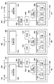
図7は、実施形態に係る複合機100のメインコントローラ部200のリングバススイッチ220の構成を説明するブロック図である。尚、拡張コントローラ部201のリングバススイッチ221の構成もこれと同様である。   FIG. 7 is a block diagram illustrating the configuration of the ring bus switch 220 of the main controller unit 200 of the multifunction peripheral 100 according to the embodiment. The configuration of the ring bus switch 221 of the expansion controller unit 201 is the same as this.

リングバススイッチ220は、リングバスにおいてデータの転送先となり得る各モジュールの合計数と同じ数だけ、その内部にスイッチを有する。実施形態では、システム制御部210、プリント処理部230、ループバック処理部240、スキャン処理部250及びリングバス外部I/F280の各モジュールに対応する5つのスイッチ701〜705を有している。これらスイッチ(SW)701〜705のそれぞれは、リングバススイッチ設定部270によって設定された値(設定値)に従って、リングバスを介した接続先を切り替えることができる。これにより、システム制御部210、プリント処理部230、ループバック処理部240、スキャン処理部250、リングバス外部I/F280の、それぞれのリングバス上での接続順を自由に変更することができる。   The ring bus switch 220 has the same number of switches as the total number of modules that can be data transfer destinations in the ring bus. In the embodiment, the system control unit 210, the print processing unit 230, the loopback processing unit 240, the scan processing unit 250, and five switches 701 to 705 corresponding to the modules of the ring bus external I / F 280 are provided. Each of these switches (SW) 701 to 705 can switch the connection destination via the ring bus according to the value (set value) set by the ring bus switch setting unit 270. Thereby, the connection order of the system control unit 210, the print processing unit 230, the loopback processing unit 240, the scan processing unit 250, and the ring bus external I / F 280 on each ring bus can be freely changed.

図8は、本実施形態に係る複合機100のリングバススイッチ220(或いは221)によるリングバスの接続制御の一例を説明するブロック図である。特に図8はメインコントローラ部200内でリングバスが完結する場合、つまり拡張コントローラ部201を使用しない場合の接続制御を示している。そ
また図9は、リングバススイッチ設定部270の構成を説明するブロック図である。
FIG. 8 is a block diagram illustrating an example of ring bus connection control by the ring bus switch 220 (or 221) of the multifunction peripheral 100 according to the present embodiment. In particular, FIG. 8 shows connection control when the ring bus is completed in the main controller unit 200, that is, when the expansion controller unit 201 is not used. FIG. 9 is a block diagram illustrating the configuration of the ring bus switch setting unit 270.

リングバススイッチ設定部270は、スイッチ701〜705を制御するためのレジスタ(制御用レジスタ)910〜950を有している。そして、実施形態に係る各制御用レジスタ910,920,930,940,950は、いずれも4ビットのレジスタで構成され、例えば、ビット0(bit0)に「1」をセットした場合、「入力(1)」がそのスイッチにおける出力(Y)と接続される。同様に、ビット1に「1」をセットすると、「入力2(2)」が、ビット2に「1」をセットすると「入力3(3)」が、ビット3に「1」をセットすると「入力4(4)」がそれぞれ、そのスイッチの出力(Y)と接続される。このように、各制御用レジスタに格納された値に従って、各スイッチにおける入力データの転送先となるモジュールが特定される。リングバス上の図8に示す接続制御を行う場合の設定値(各制御用レジスタの値)は以下の通りである。   The ring bus switch setting unit 270 includes registers (control registers) 910 to 950 for controlling the switches 701 to 705. Each of the control registers 910, 920, 930, 940, and 950 according to the embodiment is a 4-bit register. For example, when “1” is set in bit 0 (bit 0), “input ( 1) "is connected to the output (Y) at that switch. Similarly, when “1” is set to bit 1, “input 2 (2)” is set, “1” is set to bit 2, “input 3 (3)” is set, and “1” is set to bit 3, “ Each of the inputs 4 (4) "is connected to the output (Y) of the switch. In this way, the module that is the transfer destination of the input data in each switch is specified according to the value stored in each control register. The set values (values of the respective control registers) when performing the connection control shown in FIG. 8 on the ring bus are as follows.

スイッチ701制御用レジスタ(910)の値…1000(入力4を選択)
スイッチ702制御用レジスタ(920)の値…1000(入力4を選択)
スイッチ703制御用レジスタ(930)の値…0010(入力2を選択)
スイッチ704制御用レジスタ(940)の値…0010(入力2を選択)
スイッチ705制御用レジスタ(950)の値…0000(入力の選択なし)
つまり、図8のように接続する場合、スイッチ701は、設定値「1000」に従って「入力4」に対応するスキャン処理部250からのパケットデータをシステム制御部210へ出力する。スイッチ702は設定値「1000」に従って、「入力4」に対応するシステム制御部210からのパケットデータをプリント処理部230へ出力する。またスイッチ703は設定値「0010」に従って、「入力2」に対応するプリント処理部230からのパケットデータをループバック処理部240へ出力する。更にスイッチ704は設定値「0010」に従って、「入力2」に対応するループバック処理部240からのパケットデータをスキャン処理部250へ出力する。そしてスイッチ705は、設定値「0000」に従って何も出力もしない(リングバス外部I/F280が不使用となる)。
Value of switch 701 control register (910)... 1000 (input 4 selected)
Value of switch 702 control register (920)... 1000 (input 4 selected)
Value of switch 703 control register (930)... 0010 (selects input 2)
Value of switch 704 control register (940)... 0010 (selects input 2)
Value of switch 705 control register (950)... 0000 (no input selection)
That is, in the case of connection as shown in FIG. 8, the switch 701 outputs packet data from the scan processing unit 250 corresponding to “input 4” to the system control unit 210 according to the set value “1000”. The switch 702 outputs packet data from the system control unit 210 corresponding to “input 4” to the print processing unit 230 according to the set value “1000”. The switch 703 outputs packet data from the print processing unit 230 corresponding to “input 2” to the loopback processing unit 240 according to the set value “0010”. Further, the switch 704 outputs the packet data from the loopback processing unit 240 corresponding to “input 2” to the scan processing unit 250 according to the set value “0010”. The switch 705 does not output anything according to the set value “0000” (the ring bus external I / F 280 is not used).

このようにリングバススイッチ220を制御することで、システム制御部210を起点としてパケットデータは、プリント処理部230、ループバック処理部240、スキャン処理部250へと順次回り、システム制御部210へと戻る。これにより、メインコントローラ部200単体での構成、つまり拡張コントローラ部201を使用しない構成となる。   By controlling the ring bus switch 220 in this manner, the packet data starts from the system control unit 210 as a starting point, and sequentially passes to the print processing unit 230, the loopback processing unit 240, and the scan processing unit 250, and returns to the system control unit 210. Return. As a result, the main controller unit 200 alone is configured, that is, the extended controller unit 201 is not used.

図10は、実施形態に係る複合機100のメインコントローラ部200と拡張コントローラ部201とが接続されてリングバスを形成する場合の接続制御を説明する図である。ここで、図10に示す接続制御を行う場合の設定値(各制御用レジスタの値)は以下の通りである。   FIG. 10 is a diagram illustrating connection control when the main controller unit 200 and the expansion controller unit 201 of the multifunction peripheral 100 according to the embodiment are connected to form a ring bus. Here, the set values (values of the respective control registers) when performing the connection control shown in FIG. 10 are as follows.

スイッチ701制御用レジスタ(910)の値…1000(入力4を選択)
スイッチ702制御用レジスタ(920)の値…1000(入力4を選択)
スイッチ703制御用レジスタ(930)の値…0000(入力の選択なし)
スイッチ704制御用レジスタ(940)の値…0001(入力1を選択)
スイッチ705制御用レジスタ(950)の値…0010(入力2を選択)
スイッチ711制御用レジスタの値…0000(入力の選択なし)
スイッチ712制御用レジスタの値…0000(入力の選択なし)
スイッチ713制御用レジスタの値…0001(入力1を選択)
スイッチ714制御用レジスタの値…0000(入力の選択なし)
スイッチ715制御用レジスタの値…0100(入力3を選択)
つまり、図10に示すように接続する場合、スイッチ701は設定値「1000」に従って、「入力4」に対応するスキャン処理部250からのパケットデータをシステム制御部210へ出力する。スイッチ702は設定値「1000」に従って、「入力4」に対応するシステム制御部210からのパケットデータをプリント処理部230へ出力する。スイッチ703は設定値「0000」に従って何も出力もしない(ループバック処理部240が不使用となる)。スイッチ704は設定値「0001」に従って、「入力1」に対応するリングバス外部I/F280からのパケットデータをスキャン処理部250へ出力する。スイッチ705は設定値「0010」に従って、「入力2」に対応するプリント処理部230からのパケットデータをリングバス外部I/F280へ出力する。
Value of switch 701 control register (910)... 1000 (input 4 selected)
Value of switch 702 control register (920)... 1000 (input 4 selected)
Value of switch 703 control register (930)... 0000 (no input selection)
Value of switch 704 control register (940)... 0001 (select input 1)
Value of switch 705 control register (950)... 0010 (selects input 2)
Switch 711 control register value 0000 (no input selection)
Switch 712 control register value 0000 (no input selection)
Switch 713 control register value ... 0001 (input 1 selected)
Switch 714 control register value ... 0000 (no input selection)
Switch 715 control register value ... 0100 (input 3 selected)
That is, when connecting as shown in FIG. 10, the switch 701 outputs packet data from the scan processing unit 250 corresponding to “input 4” to the system control unit 210 according to the set value “1000”. The switch 702 outputs packet data from the system control unit 210 corresponding to “input 4” to the print processing unit 230 according to the set value “1000”. The switch 703 does not output anything according to the set value “0000” (the loopback processing unit 240 is not used). The switch 704 outputs packet data from the ring bus external I / F 280 corresponding to “input 1” to the scan processing unit 250 according to the set value “0001”. The switch 705 outputs packet data from the print processing unit 230 corresponding to “input 2” to the ring bus external I / F 280 according to the set value “0010”.

このようにリングバススイッチ220を制御することで、システム制御部210を起点としてパケットデータは、プリント処理部230、リングバス外部I/F280、スキャン処理部250へと順次回り、システム制御部210へと戻る。   By controlling the ring bus switch 220 in this way, the packet data starts from the system control unit 210, and sequentially passes to the print processing unit 230, the ring bus external I / F 280, and the scan processing unit 250, and then to the system control unit 210. And return.

また拡張コントローラ部201のリングバススイッチ221では、スイッチ711,712及び714は設定値「0000」に従って何も出力もしない(システム制御部211、プリント処理部231、スキャン処理部251が不使用となる)。スイッチ713は設定値「0001」に従って、「入力1」に対応するリングバス外部I/F281からのパケットデータをループバック処理部241へ出力する。スイッチ715は設定値「0100」に従って、「入力3」に対応するループバック処理部241からのパケットデータをリングバス外部I/F281へ出力する。   In the ring bus switch 221 of the extended controller unit 201, the switches 711, 712, and 714 do not output anything according to the set value “0000” (the system control unit 211, the print processing unit 231, and the scan processing unit 251 are not used). ). The switch 713 outputs packet data from the ring bus external I / F 281 corresponding to “input 1” to the loopback processing unit 241 according to the set value “0001”. The switch 715 outputs the packet data from the loopback processing unit 241 corresponding to “input 3” to the ring bus external I / F 281 according to the set value “0100”.

このようにリングバススイッチ221を制御することで、拡張コントローラ部201へ入力されたパケットデータは、ループバック処理部241を経由してメインコントローラ部200へ戻る。即ち、システム制御部210を起点としてパケットデータが、プリント処理部230、ループバック処理部241、スキャン処理部250へと順次経由してシステム制御部210へ戻るリングバスを形成することが可能となる。   By controlling the ring bus switch 221 in this way, the packet data input to the expansion controller unit 201 returns to the main controller unit 200 via the loopback processing unit 241. That is, it is possible to form a ring bus in which packet data starts from the system control unit 210 and returns to the system control unit 210 via the print processing unit 230, the loopback processing unit 241, and the scan processing unit 250 in order. .

以上のようにリングバスを形成することにより、メインコントローラ部200のループバック処理部240を使用しないことにより、RAM291bへのデータ転送路の混雑が緩和され、メインコントローラ部200の性能低下を防ぐことが可能となる。   By forming the ring bus as described above, the loopback processing unit 240 of the main controller unit 200 is not used, so that congestion of the data transfer path to the RAM 291b is alleviated and performance degradation of the main controller unit 200 is prevented. Is possible.

尚、実施形態においては、メインコントローラ部200及び拡張コントローラ部201の外部から、これらレジスタの値を設定/変更できるようにしても良い。例えば、上述のリングバススイッチ制御用レジスタの値を編集可能なソフトウェアを用いて、ユーザが操作部130を介して新たな値を設定できるような構成でもよい。その場合、そのソフトウェアは、システム制御部210のCPU310が実行し、拡張コントローラ部201のシステム制御部211は使用しない。そのため、拡張コントローラ部201のリングバススイッチ設定部271における制御用レジスタ値の変更についても、メインコントローラ部200のシステム制御部210が、リングバス外部I/F280及び281を介して行なうことになる。   In the embodiment, the values of these registers may be set / changed from outside the main controller unit 200 and the extended controller unit 201. For example, the configuration may be such that the user can set a new value via the operation unit 130 using software capable of editing the value of the above-described ring bus switch control register. In that case, the software is executed by the CPU 310 of the system control unit 210 and the system control unit 211 of the expansion controller unit 201 is not used. Therefore, the system control unit 210 of the main controller unit 200 also changes the control register value in the ring bus switch setting unit 271 of the extended controller unit 201 via the ring bus external I / Fs 280 and 281.

尚、実施形態では、拡張コントローラ部201の構成はメインコントローラ部200と同じ構成としているが、一部が異なる構成でも構わない。また実施形態では、メインコントローラ部200と拡張コントローラ部201とにそれぞれリングバススイッチ設定部270,271を備える構成としたが、本発明はこれに限定されない。例えば、共通する1個のリングバススイッチ設定部によって、リングバススイッチ220,221双方のスイッチ制御を行う構成であっても構わない。   In the embodiment, the configuration of the extended controller unit 201 is the same as that of the main controller unit 200, but a part of the configuration may be different. In the embodiment, the main controller unit 200 and the expansion controller unit 201 are each provided with the ring bus switch setting units 270 and 271, but the present invention is not limited to this. For example, the switch control of both the ring bus switches 220 and 221 may be performed by one common ring bus switch setting unit.

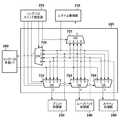
図11は、実施形態に係る複合機100のメインコントローラ部200の帯域モニタ295の構成を説明するブロック図である。   FIG. 11 is a block diagram illustrating the configuration of the bandwidth monitor 295 of the main controller unit 200 of the multifunction peripheral 100 according to the embodiment.

帯域モニタ295は、帯域検出部1101、帯域通知部1102、帯域閾値設定部1103、及び割り込み通知部1104を有している。帯域モニタ295は、メインコントローラ部200のRAM291bのメモリ帯域を測定するために用いられる。即ち、メインコントローラ部200のプリント処理部230、ループバック処理部240、スキャン処理部250の各処理部と、RAMコントローラ260との間のデータ転送を帯域検出部1101によりモニタする。そして、RAM291bの、その時点でのメモリ帯域を算出する。こうして帯域検出部1101により取得されたメインコントローラ部200のRAM291bのメモリ帯域は、帯域通知部1102を通してCPU310により読み取り可能である。   The bandwidth monitor 295 includes a bandwidth detection unit 1101, a bandwidth notification unit 1102, a bandwidth threshold setting unit 1103, and an interrupt notification unit 1104. The bandwidth monitor 295 is used to measure the memory bandwidth of the RAM 291b of the main controller unit 200. That is, the band detection unit 1101 monitors data transfer between the print processing unit 230 of the main controller unit 200, the loopback processing unit 240, and the processing units of the scan processing unit 250 and the RAM controller 260. Then, the memory bandwidth at that time of the RAM 291b is calculated. The memory band of the RAM 291b of the main controller unit 200 acquired by the band detection unit 1101 in this way can be read by the CPU 310 through the band notification unit 1102.

帯域閾値設定部1103は、CPU310により帯域の閾値(所定値)が設定される。帯域閾値設定部1103に設定された閾値は、帯域検出部1101により計測されたRAM291bの、その時点でのメモリ帯域との比較に用いられる。そのときのメモリ帯域が、帯域閾値設定部1103に設定された閾値よりも大きい場合、割り込み通知部1104を通してCPU310に通知することも可能である。実際の使用例として、帯域閾値設定部1103には、先述したようなメモリデバイスや動作周波数で決まるRAM291bのメモリ帯域性能の上限値、或いは上限値に近い値を設定する。そして、プリント処理部230、ループバック処理部240及びスキャン処理部250を使用する時に、帯域検出部1101が示す、RAM291bのメモリ帯域との比較に用いられる。帯域検出部1101が示すRAM291bの使用メモリ帯域が、帯域閾値設定部1103に設定した閾値より大きい場合、メインコントローラ部200のRAM291bが混雑していると判断し、拡張コントローラ部201へ電源供給を開始する。そして、リアルタイム性が要求されていないループバック処理部240を使用する画像処理を、拡張コントローラ部201のループバック処理部241へ割り当てる。これにより、メインコントローラ部201のRAM291bの混雑を少なくし、リアルタイム処理が待たされたり、或いは遅延するのを防止できる。もちろん、各画像処理を行う時に、帯域検出部1101が示すRAM291bの使用メモリ帯域と、これから実行する画像処理で使用するメモリ帯域の予想値との合計値を、帯域閾値設定部1103に設定した閾値との比較に用いてもよい。こうすることにより、これから実行する画像処理を行った場合に、RAM291bのメモリ帯域が、RAM291bのメモリ帯域性能の上限値に達してしまうかどうかを事前に判断できる。   In the bandwidth threshold setting unit 1103, a bandwidth threshold (predetermined value) is set by the CPU 310. The threshold set in the band threshold setting unit 1103 is used for comparison with the memory band at that time of the RAM 291b measured by the band detection unit 1101. When the memory bandwidth at that time is larger than the threshold set in the bandwidth threshold setting unit 1103, the CPU 310 can be notified through the interrupt notification unit 1104. As an actual usage example, the upper limit value of the memory band performance of the RAM 291b determined by the memory device and the operating frequency as described above or a value close to the upper limit value is set in the band threshold setting unit 1103. When the print processing unit 230, the loopback processing unit 240, and the scan processing unit 250 are used, it is used for comparison with the memory band of the RAM 291b indicated by the band detection unit 1101. If the used memory band of the RAM 291b indicated by the band detection unit 1101 is larger than the threshold set in the band threshold setting unit 1103, it is determined that the RAM 291b of the main controller unit 200 is congested, and power supply to the expansion controller unit 201 is started. To do. Then, image processing using the loopback processing unit 240 that is not required to be real-time is assigned to the loopback processing unit 241 of the extended controller unit 201. As a result, congestion of the RAM 291b of the main controller unit 201 can be reduced, and real-time processing can be prevented from being delayed or delayed. Of course, when each image processing is performed, the threshold value set in the bandwidth threshold setting unit 1103 is the total value of the memory bandwidth used by the RAM 291b indicated by the bandwidth detection unit 1101 and the expected value of the memory bandwidth used in the image processing to be executed in the future. You may use for comparison with. By doing so, it is possible to determine in advance whether the memory bandwidth of the RAM 291b will reach the upper limit value of the memory bandwidth performance of the RAM 291b when image processing to be executed is performed.

一方、帯域検出部1101が示すRAM291bの使用メモリ帯域が、帯域閾値設定部1103に設定した閾値以下(所定値以下)の場合、RAM291bの帯域は混雑していないと判断し、これから実行する処理をメインコントローラ部201に割り当てる。これにより、RAM291bのメモリ帯域に鑑み、メモリ帯域性能に影響がある場合のみ、拡張コントローラ部201を使用することが可能となる。   On the other hand, if the used memory bandwidth of the RAM 291b indicated by the bandwidth detection unit 1101 is less than or equal to the threshold set in the bandwidth threshold setting unit 1103 (below a predetermined value), it is determined that the bandwidth of the RAM 291b is not congested, and the processing to be executed from now on is determined. Assigned to the main controller unit 201. Thereby, in view of the memory bandwidth of the RAM 291b, the extended controller unit 201 can be used only when the memory bandwidth performance is affected.

このように、帯域モニタ295により、CPU310は、RAM291bのメモリ帯域を知ることができ、それを拡張コントローラ部201を使用するか否かの判定に用いることができる。   As described above, the bandwidth monitor 295 allows the CPU 310 to know the memory bandwidth of the RAM 291b and use it to determine whether or not to use the extended controller unit 201.

図12は、実施形態に係る複合機100におけるメインコントローラ部200と拡張コントローラ部201による処理の制御を説明するフローチャートである。尚、このフローチャートで示す処理は、CPU310がHDD292に格納されたプログラムをRAM291aに展開し、CPU310が、その展開したプログラムを実行することにより達成される。   FIG. 12 is a flowchart for explaining control of processing by the main controller unit 200 and the expansion controller unit 201 in the multifunction peripheral 100 according to the embodiment. Note that the processing shown in this flowchart is achieved when the CPU 310 expands the program stored in the HDD 292 to the RAM 291a, and the CPU 310 executes the expanded program.

まずS1201でCPU310は、ジョブを受付けたかどうか判定する。ここでは例えば、ユーザからスキャンジョブやFAX送信ジョブを受付ける場合は、ユーザが操作部130を操作したことを操作部インタフェース340を介してCPU310が検知し、その操作内容に従ってジョブの入力を受け付ける。また、PC等からのプリントジョブの受信の場合は、ネットワーク150及びLANコントローラ370経由でCPU310はホストコンピュータからのジョブの入力を受け付ける。またFAX受信ジョブであれば、公衆回線及びモデム372を介してCPU310はジョブの入力を受け付ける。こうしてジョブを受け付けるとS1202へ進む。S1202でCPU310は、S1201で受け付けたジョブにより使用される画像処理機能を判定してS1203に進む。具体的には、プリント処理部230、ループバック処理部240、スキャン処理部250のどの処理が、受け付けたジョブによって使用されるかを判定する。   In step S1201, the CPU 310 determines whether a job has been received. Here, for example, when a scan job or FAX transmission job is received from the user, the CPU 310 detects that the user has operated the operation unit 130 via the operation unit interface 340, and receives a job input according to the operation content. When receiving a print job from a PC or the like, the CPU 310 receives an input of a job from the host computer via the network 150 and the LAN controller 370. If the job is a FAX reception job, the CPU 310 receives an input of the job via the public line and the modem 372. When the job is received in this way, the process proceeds to S1202. In step S1202, the CPU 310 determines an image processing function used by the job received in step S1201, and proceeds to step S1203. Specifically, it is determined which process of the print processing unit 230, the loopback processing unit 240, and the scan processing unit 250 is used by the received job.

例えば、ジョブとしてFAX送信ジョブを受け付けた場合、FAX送信のためにスキャナ部110を用いたスキャン処理を実行するためスキャン処理部250が使用される。またスキャンした画像データに対してFAX送信可能なフォーマットに変換するためにループバック処理部240が使用される。具体的には、2値化処理部711による送信画像の2値化処理、及び解像度変換部713によるFAX送信可能な解像度の画像データへの変換処理が実行される。つまり、スキャン処理部250とループバック処理部240の2つの画像処理部が使用されると判定する。   For example, when a FAX transmission job is accepted as a job, the scan processing unit 250 is used to execute a scan process using the scanner unit 110 for FAX transmission. A loopback processing unit 240 is used to convert scanned image data into a format that can be transmitted by FAX. Specifically, a binarization process of a transmission image by the binarization processing unit 711 and a conversion process to image data having a resolution capable of FAX transmission by a resolution conversion unit 713 are executed. That is, it is determined that two image processing units, the scan processing unit 250 and the loopback processing unit 240, are used.

また、ホストコンピュータからプリントジョブを受け付けた場合、プリンタ部140を用いたプリント処理を実行するためプリント処理部230が使用される。また例えば、ホストコンピュータから送付されてきたプリントすべき画像データと、給紙部142にセットされている記録紙の向きが異なる場合は、ループバック処理部240の回転処理部710を使用して画像データの向きを回転させる。また例えば、地紋などのデータを画像データに合成する指示があった場合は、ループバック処理部240の画像合成部714を使用して、画像データに地紋データを合成する。この場合は、プリント処理部230とループバック処理部240の2つの画像処理部が使用される。   When a print job is received from the host computer, the print processing unit 230 is used to execute print processing using the printer unit 140. Further, for example, when the image data to be printed sent from the host computer and the orientation of the recording paper set in the paper feeding unit 142 are different, the image is processed using the rotation processing unit 710 of the loopback processing unit 240. Rotate the data direction. Also, for example, when there is an instruction to synthesize data such as a tint block pattern with image data, the image pattern unit 714 of the loopback processing unit 240 is used to synthesize the tint block data with the image data. In this case, two image processing units, the print processing unit 230 and the loopback processing unit 240, are used.

デジタル複合機100は一般的に、複数のジョブを同時に受け付けることができ、ジョブが重なる状態をジョブ競合状態と呼ぶ。ジョブ競合状態は、例えばデジタル複合機100がプリントジョブとFAX送信ジョブとをほぼ同時に受け付けた場合などに発生し、複数のジョブが競合した場合に、前述したRAM291bへのデータ転送路が混雑することとなる。   In general, the digital multi-function peripheral 100 can accept a plurality of jobs at the same time, and a state where jobs overlap is called a job conflict state. The job conflict state occurs, for example, when the digital multi-function peripheral 100 accepts a print job and a FAX transmission job almost simultaneously. When a plurality of jobs compete, the data transfer path to the RAM 291b is congested. It becomes.

S1203でCPU310は、S1202で判定した画像処理を実行する前に、帯域モニタ295が示すRAM291bの現在のメモリ帯域を確認する。ここで、この帯域モニタ295が示すRAM291bの帯域が、閾値より小さければ、RAM291bは混雑していないと判定してS1204へ進み、閾値以上であればRAM291bは混雑していると判定してS1205へ進む。ここで言う閾値は、帯域モニタの説明で前述したように、メモリデバイスや動作周波数で決まるRAM291bのメモリ帯域性能の上限値、或いは上限値に近い値である。もちろん、各画像処理を行う時に、帯域モニタ295が示すRAM291bの現在のメモリ帯域と、これから実行する画像処理で使用するメモリ帯域の予想値との合計値を、閾値との比較に用いてもよい。こうすることにより、これから実行する画像処理を行った場合に、RAM291bのメモリ帯域が、RAM291bのメモリ帯域性能の上限値に達してしまうかどうかを事前に判定できる。   In step S1203, the CPU 310 checks the current memory bandwidth of the RAM 291b indicated by the bandwidth monitor 295 before executing the image processing determined in step S1202. If the bandwidth of the RAM 291b indicated by the bandwidth monitor 295 is smaller than the threshold, it is determined that the RAM 291b is not congested, and the process proceeds to S1204. If it is equal to or greater than the threshold, it is determined that the RAM 291b is congested and the process proceeds to S1205. move on. As described above in the description of the bandwidth monitor, the threshold here is the upper limit value of the memory bandwidth performance of the RAM 291b determined by the memory device and the operating frequency, or a value close to the upper limit value. Of course, when performing each image processing, the total value of the current memory bandwidth of the RAM 291b indicated by the bandwidth monitor 295 and the expected value of the memory bandwidth used for the image processing to be executed in the future may be used for comparison with the threshold value. . By doing so, it is possible to determine in advance whether the memory bandwidth of the RAM 291b reaches the upper limit value of the memory bandwidth performance of the RAM 291b when image processing to be executed is performed.

S1204でCPU310は、リングバススイッチ220を、メインコントローラ部200でリングバスが完結する状態に設定してS1209に進む。このS1204は、CPU310が、メインコントローラ部200のRAM291bへのデータ転送路が混雑していないと判定した場合に実施されるため、図8で示したように拡張コントローラ部201を使用しないようリングバススイッチ220を設定する。   In S1204, the CPU 310 sets the ring bus switch 220 to a state in which the ring bus is completed in the main controller unit 200, and proceeds to S1209. This S1204 is performed when the CPU 310 determines that the data transfer path to the RAM 291b of the main controller unit 200 is not congested, so that the ring bus is not used as shown in FIG. Switch 220 is set.

一方、S1205でCPU310は、拡張コントローラ部201への電源供給を開始する。具体的にはCPU310は、GPIO制御部390を制御してGPIO信号をハイレベルにする。これによりコントローラ部120の電源供給部294は、拡張コントローラ部201への電源供給を開始する。   On the other hand, in step S1205, the CPU 310 starts supplying power to the expansion controller unit 201. Specifically, the CPU 310 controls the GPIO control unit 390 to set the GPIO signal to a high level. As a result, the power supply unit 294 of the controller unit 120 starts supplying power to the expansion controller unit 201.

次にS1206に進みCPU310は、リングバス外部I/F280を介してメインコントローラ部200と拡張コントローラ部201との間でパケットデータを送受信可能となるようにリングバススイッチ220及び221を設定する。具体的な設定は、例えば図10で示したものとなる。このS1206は、メインコントローラ部200のRAM291bへのデータ転送路が混雑していると判定された場合に実施されるため、図10で示したように拡張コントローラ部201を使用できるようリングバススイッチ220及び221を設定する。次にS1207に進みCPU310は、拡張コントローラ部201の初期設定を実行する。この初期設定は、ループバック処理部241及びRAMコントローラ261の設定である。本実施形態では、CPU310はパケットデータを拡張コントローラ部201へ送信することで拡張コントローラ部201の各種設定を行う。次にS1208に進みCPU310は、ループバック画像処理を拡張コントローラ部201のループバック処理部241に割り当ててS1209に進む。S1208では、メインコントローラ部200のRAM291bへのデータ転送路が混雑していると判定されているため、更に画像処理を同時実行した場合にRAM291bのメモリ帯域性能の上限値に達してしまう可能性がある。そのため、プリント処理部230及びスキャン処理部250に対して、リアルタイム性を求められないループバック処理の画像処理を、拡張コントローラ部201のループバック処理部241に割り当てる。この時、他のジョブによりメインコントローラ部200のループバック処理部240が既に使用されていた場合は、ループバック処理部240の処理を停止し、拡張コントローラ201のループバック処理部241に、再度、その画像処理を割り当てる。   In step S1206, the CPU 310 sets the ring bus switches 220 and 221 so that packet data can be transmitted and received between the main controller unit 200 and the expansion controller unit 201 via the ring bus external I / F 280. Specific settings are as shown in FIG. 10, for example. Since this S1206 is performed when it is determined that the data transfer path to the RAM 291b of the main controller unit 200 is congested, the ring bus switch 220 is used so that the extended controller unit 201 can be used as shown in FIG. And 221 are set. In step S <b> 1207, the CPU 310 executes initial setting of the extended controller unit 201. This initial setting is a setting of the loopback processing unit 241 and the RAM controller 261. In this embodiment, the CPU 310 performs various settings of the extended controller unit 201 by transmitting packet data to the extended controller unit 201. The process advances to step S1208, and the CPU 310 assigns the loopback image processing to the loopback processing unit 241 of the extended controller unit 201, and advances to step S1209. In S1208, since it is determined that the data transfer path to the RAM 291b of the main controller unit 200 is congested, there is a possibility that the upper limit value of the memory bandwidth performance of the RAM 291b will be reached when image processing is further executed simultaneously. is there. Therefore, for the print processing unit 230 and the scan processing unit 250, the image processing of the loop back processing that does not require real-time property is assigned to the loop back processing unit 241 of the extended controller unit 201. At this time, if the loopback processing unit 240 of the main controller unit 200 has already been used by another job, the processing of the loopback processing unit 240 is stopped, and the loopback processing unit 241 of the expansion controller 201 is again sent to Assign the image processing.

S1209でCPU310は、デジタル複合機100の各部を制御し、受け付けたジョブに対する画像処理を実行する。このときS1204からS1209に進んだ場合は、画像処理はコントローラ部120のメインコントローラ部200のみを用いて実行され、このとき拡張コントローラ部201には電源が供給されていない。またS1208からS1209に進んだ場合は、コントローラ部120において、メインコントローラ部200及び拡張コントローラ部201の両方を用いて画像処理が実行される。   In step S1209, the CPU 310 controls each unit of the digital multi-function peripheral 100, and executes image processing for the received job. At this time, if the process proceeds from S1204 to S1209, the image processing is executed using only the main controller unit 200 of the controller unit 120, and at this time, power is not supplied to the extended controller unit 201. When the process proceeds from S1208 to S1209, the controller unit 120 executes image processing using both the main controller unit 200 and the extended controller unit 201.

次にS1210に進みCPU310は、S1209で実行している画像処理が終了したか否かを判定し、画像処理が終了したと判定するとS1211へ進むが、そうでないときはS1210を実行する。S1211でCPU310は、拡張コントローラ部201のループバック処理部241が他のジョブで使用されているかどうか判定する。ここで他のジョブを受け付けて拡張コントローラ部201のループバック処理部241が使用されているときは、継続して拡張コントローラ部201を使用するようにして、この処理を終了する。   The process advances to step S1210, and the CPU 310 determines whether the image processing being executed in step S1209 has ended. If it is determined that the image processing has ended, the process advances to step S1211. If not, the CPU 310 executes step S1210. In step S <b> 1211, the CPU 310 determines whether the loopback processing unit 241 of the extended controller unit 201 is used in another job. Here, when another job is received and the loopback processing unit 241 of the extended controller unit 201 is used, the extended controller unit 201 is continuously used, and this process is terminated.

一方、S1211でCPU301は、拡張コントローラ部201のループバック処理部241が使用されていないと判定するとS1212に進む。S1212でCPU310は、リングバススイッチ220及び221を、拡張コントローラ部201を使用しない図8の状態に戻す。そしてS1213に進みCPU310は、拡張コントローラ部201の電源供給を停止する。具体的にはCPU310は、GPIO制御部390を制御してGPIO信号をロウレベルにする。これにより電源供給部294は、拡張コントローラ部201への電源供給を停止する。これにより拡張コントローラ部201は、再び省電力状態へと戻る。   On the other hand, if the CPU 301 determines in step S1211 that the loopback processing unit 241 of the extended controller unit 201 is not used, the process advances to step S1212. In step S <b> 1212, the CPU 310 returns the ring bus switches 220 and 221 to the state illustrated in FIG. 8 in which the extended controller unit 201 is not used. In step S1213, the CPU 310 stops the power supply to the expansion controller unit 201. Specifically, the CPU 310 controls the GPIO control unit 390 to set the GPIO signal to a low level. As a result, the power supply unit 294 stops the power supply to the expansion controller unit 201. As a result, the extended controller unit 201 returns to the power saving state again.

以上説明したように実施形態によれば、メインコントローラ部200のRAM291bのメモリ帯域が、メモリ帯域性能の上限値に近づいた場合に、拡張コントローラ部へ電源を供給して、拡張コントローラ部により、機能の一部を代替させる。これにより、必要最低限、拡張コントローラ部を使用して、受け付けたジョブを実行させることができる。   As described above, according to the embodiment, when the memory band of the RAM 291b of the main controller unit 200 approaches the upper limit value of the memory band performance, power is supplied to the expansion controller unit, and the function is performed by the expansion controller unit. Substitute part of As a result, the accepted job can be executed using the extended controller unit at the minimum.

実施形態によれば、帯域モニタ295が示すメモリ帯域性能に鑑みて、拡張コントローラ部201が省電力状態から復帰するよう制御することで、拡張コントローラ部201を使用する期間を最小限にできる。これにより、動作中のコントローラ部120の消費電力を低減させることが可能となる。   According to the embodiment, in view of the memory bandwidth performance indicated by the bandwidth monitor 295, the period during which the extended controller unit 201 is used can be minimized by controlling the extended controller unit 201 to return from the power saving state. Thereby, it becomes possible to reduce the power consumption of the controller unit 120 in operation.

複数のプロセッサに処理を分散する場合、プロセスの数のみに基づいて、各プロセッサの負荷状況を判断する。そして、各プロセッサによるメモリアクセスの競合状態に関しては、各プロセスで使用するメモリ帯域の机上の計算値の合計に基づいて設計をする必要がある。このため、実際のメモリアクセスの競合の度合いに対して、マージンを持たせて設計する必要がある。従って、全体の消費電力を低減させるには限界がある。   When processing is distributed to a plurality of processors, the load status of each processor is determined based only on the number of processes. The memory access contention state by each processor needs to be designed based on the sum of the calculated values on the desk of the memory bandwidth used in each process. For this reason, it is necessary to design with a margin with respect to the actual competition degree of memory access. Therefore, there is a limit to reducing the overall power consumption.

これに対して実施形態では、バス帯域モニタ295で動的にモニタされたメモリ帯域を使用するため、実際に使用されているメモリ帯域に基づいて拡張コントローラ部を使用するか、しないかを判定できる。これにより、より効率的に、拡張コントローラ部を省電力状態に留まらせることができ、装置全体の消費電力を、より低減させることができる。   On the other hand, in the embodiment, since the memory bandwidth dynamically monitored by the bus bandwidth monitor 295 is used, it can be determined whether or not to use the expansion controller unit based on the actually used memory bandwidth. . Thereby, the extended controller unit can be more efficiently kept in the power saving state, and the power consumption of the entire apparatus can be further reduced.

(その他の実施形態)
本発明は、上述の実施形態の1以上の機能を実現するプログラムを、ネットワーク又は記憶媒体を介してシステム又は装置に供給し、そのシステム又は装置のコンピュータにおける1つ以上のプロセッサーがプログラムを読出し実行する処理でも実現可能である。また、1以上の機能を実現する回路(例えば、ASIC)によっても実現可能である。
(Other embodiments)
The present invention supplies a program that realizes one or more functions of the above-described embodiments to a system or apparatus via a network or a storage medium, and one or more processors in a computer of the system or apparatus read and execute the program This process can be realized. It can also be realized by a circuit (for example, ASIC) that realizes one or more functions.

本発明は上記実施形態に制限されるものではなく、本発明の精神及び範囲から離脱することなく、様々な変更及び変形が可能である。従って、本発明の範囲を公にするために、以下の請求項を添付する。   The present invention is not limited to the above-described embodiment, and various changes and modifications can be made without departing from the spirit and scope of the present invention. Therefore, in order to make the scope of the present invention public, the following claims are attached.

100…複合機、120…コントローラ部、200…メインコントローラ部、201…拡張コントローラ部、210…システム制御部、220,221…リングバススイッチ、270,271…リングバススイッチ設定部、294…電源供給部、295…帯域モニタ、310…CPU   DESCRIPTION OF SYMBOLS 100 ... MFP, 120 ... Controller part, 200 ... Main controller part, 201 ... Expansion controller part, 210 ... System control part, 220, 221 ... Ring bus switch, 270, 271 ... Ring bus switch setting part, 294 ... Power supply Part, 295 ... band monitor, 310 ... CPU

Claims (12)

複数の処理部を有する第1の制御部と、
前記複数の処理部と少なくとも一つと共通する処理を実行できる第1処理部を含む複数の処理部を有する第2制御部と、
前記第1及び第2の制御部への電源供給を制御する電源供給手段と、
前記第1の制御部の前記複数の処理部の少なくとも一つを使用してジョブを実行する際、当該ジョブの実行に使用される処理部とメモリとの間のメモリ帯域性能を測定する測定手段と、
前記測定手段により測定された前記メモリ帯域性能が所定値よりも大きい場合は、前記第1の制御部の複数の処理部の少なくとも一つにより実行される処理を、前記第1処理部に代替させ、前記測定手段により測定された前記メモリ帯域性能が所定値以下の場合は、前記電源供給手段により前記第2の制御部への電源供給を停止させるように制御する制御手段と、
を有することを特徴とする画像処理装置。
A first control unit having a plurality of processing units;
A second control unit having a plurality of processing units including a first processing unit capable of executing processing common to at least one of the plurality of processing units;
Power supply means for controlling power supply to the first and second control units;
Measuring means for measuring memory bandwidth performance between a processing unit and a memory used for execution of the job when executing a job using at least one of the plurality of processing units of the first control unit When,
When the memory bandwidth performance measured by the measuring unit is greater than a predetermined value, the first processing unit is substituted for processing executed by at least one of the plurality of processing units of the first control unit. Control means for controlling the power supply means to stop power supply to the second control unit when the memory bandwidth performance measured by the measurement means is less than or equal to a predetermined value;
An image processing apparatus comprising:
前記メモリ帯域性能は、前記第1の制御部の複数の処理部と前記メモリとを接続するバスにおける単位時間当たりのデータ転送量であることを特徴とする請求項1に記載の画像処理装置。   The image processing apparatus according to claim 1, wherein the memory bandwidth performance is a data transfer amount per unit time in a bus connecting the plurality of processing units of the first control unit and the memory. 前記制御手段は、前記測定手段により測定された前記メモリ帯域性能が所定値よりも大きくなることに応じて、前記第1の制御部の複数の処理部の少なくとも一つにより実行される処理の内、リアルタイム性を求められない処理を前記第1処理部に代替させることを特徴とする請求項1又は2に記載の画像処理装置。   The control unit includes a process executed by at least one of the plurality of processing units of the first control unit in response to the memory bandwidth performance measured by the measurement unit becoming larger than a predetermined value. The image processing apparatus according to claim 1, wherein the first processing unit substitutes a process for which real-time characteristics are not required. 前記リアルタイム性を求められない処理は、ループバック画像処理を含むことを特徴とする請求項3に記載の画像処理装置。   The image processing apparatus according to claim 3, wherein the process that does not require real-time processing includes loopback image processing. 前記第1の制御部と前記第2の制御部とはリングバスを介して接続され、前記第1の制御部の前記複数の処理部は第1のバススイッチを介して接続され、前記第2の制御部の前記複数の処理部は第2のバススイッチを介して接続され、前記制御手段は、前記第1及び第2のバススイッチの切り替えを制御することにより、前記第1の制御部の複数の処理部の少なくとも一つにより実行される処理を、前記第1処理部に代替させることを特徴とする請求項1乃至4のいずれか1項に記載の画像処理装置。   The first control unit and the second control unit are connected via a ring bus, the plurality of processing units of the first control unit are connected via a first bus switch, and the second control unit The plurality of processing units of the control unit are connected via a second bus switch, and the control means controls the switching of the first and second bus switches, thereby controlling the switching of the first control unit. 5. The image processing apparatus according to claim 1, wherein a process executed by at least one of a plurality of processing units is substituted by the first processing unit. 6. 前記第1の制御部は、前記第1のバススイッチの設定値を保持する第1保持手段を有し、前記第2の制御部は、前記第2のバススイッチの設定値を保持する第2保持手段を有することを特徴とする請求項5に記載の画像処理装置。   The first control unit includes a first holding unit that holds a set value of the first bus switch, and the second control unit is a second that holds a set value of the second bus switch. The image processing apparatus according to claim 5, further comprising a holding unit. 前記制御手段は、前記第1保持手段及び前記第2保持手段の設定値を設定することにより、前記第1の制御部の複数の処理部の少なくとも一つにより実行される処理を前記第1処理部に代替させることを特徴とする請求項6に記載の画像処理装置。   The control means sets a set value of the first holding means and the second holding means to perform a process executed by at least one of the plurality of processing units of the first control unit. The image processing apparatus according to claim 6, wherein the image processing apparatus is substituted with a unit. 前記制御手段は、前記測定手段により測定された前記メモリ帯域性能が所定値以下のとき、前記第1の制御部の処理部だけで前記ジョブを実行するように前記第1保持手段の設定値を設定することを特徴とする請求項6に記載の画像処理装置。   The control means sets the setting value of the first holding means so that the job is executed only by the processing unit of the first control unit when the memory bandwidth performance measured by the measurement unit is equal to or less than a predetermined value. The image processing apparatus according to claim 6, wherein the image processing apparatus is set. 前記測定手段は、前記第1の制御部の複数の処理部と前記メモリとの間に接続されて前記メモリのメモリ帯域性能を測定することを特徴とする請求項1乃至8のいずれか1項に記載の画像処理装置。   9. The measurement unit according to claim 1, wherein the measurement unit is connected between the plurality of processing units of the first control unit and the memory, and measures the memory bandwidth performance of the memory. An image processing apparatus according to 1. 前記第1の制御部は、前記画像処理装置に組み込まれているメインの制御部であり、前記第2の制御部は、前記メインの制御部と着脱可能な機能拡張用の制御部であることを特徴とする請求項1乃至9のいずれか1項に記載の画像処理装置。   The first control unit is a main control unit incorporated in the image processing apparatus, and the second control unit is a function expansion control unit detachable from the main control unit. The image processing apparatus according to claim 1, wherein: 複数の処理部を有する第1の制御部と、前記複数の処理部と少なくとも一つと共通する処理を実行できる第1処理部を含む複数の処理部を有する第2制御部とを有する画像処理装置を制御する制御方法であって、
前記第1の制御部の前記複数の処理部の少なくとも一つを使用してジョブを実行する際、当該ジョブの実行に使用される処理部とメモリとの間のメモリ帯域性能を測定する測定工程と、
前記測定工程で測定された前記メモリ帯域性能が所定値よりも大きい場合、前記第1の制御部の複数の処理部の少なくとも一つにより実行される処理を、前記第1処理部に代替させ、前記測定工程で測定された前記メモリ帯域性能が所定値以下の場合は前記電源供給手段により前記第2の制御部への電源供給を停止させるように制御する制御工程と、
を有することを特徴とする画像処理装置の制御方法。
An image processing apparatus comprising: a first control unit having a plurality of processing units; and a second control unit having a plurality of processing units including a first processing unit capable of executing a process common to at least one of the plurality of processing units. A control method for controlling
A measurement step of measuring memory bandwidth performance between a processing unit and a memory used for executing the job when executing a job using at least one of the plurality of processing units of the first control unit When,
If the memory bandwidth performance measured in the measurement step is larger than a predetermined value, the first processing unit is substituted for processing executed by at least one of the plurality of processing units of the first control unit, A control step of controlling the power supply means to stop power supply to the second control unit when the memory bandwidth performance measured in the measurement step is less than or equal to a predetermined value;
A control method for an image processing apparatus, comprising:
コンピュータに、請求項11に記載の制御方法の各工程を実行させるためのプログラム。   The program for making a computer perform each process of the control method of Claim 11.
JP2017012540A 2017-01-26 2017-01-26 Image processing device, control method and program of the same Withdrawn JP2018118477A (en)

Priority Applications (2)

Application Number Priority Date Filing Date Title
JP2017012540A JP2018118477A (en) 2017-01-26 2017-01-26 Image processing device, control method and program of the same
US15/876,260 US20180213103A1 (en) 2017-01-26 2018-01-22 Image processing apparatus, method of controlling the same, and storage medium

Applications Claiming Priority (1)

Application Number Priority Date Filing Date Title
JP2017012540A JP2018118477A (en) 2017-01-26 2017-01-26 Image processing device, control method and program of the same

Publications (2)

Publication Number Publication Date
JP2018118477A true JP2018118477A (en) 2018-08-02
JP2018118477A5 JP2018118477A5 (en) 2020-02-20

Family

ID=62907268

Family Applications (1)

Application Number Title Priority Date Filing Date
JP2017012540A Withdrawn JP2018118477A (en) 2017-01-26 2017-01-26 Image processing device, control method and program of the same

Country Status (2)

Country Link
US (1) US20180213103A1 (en)
JP (1) JP2018118477A (en)

Families Citing this family (1)

* Cited by examiner, † Cited by third party
Publication number Priority date Publication date Assignee Title
JP7256660B2 (en) * 2019-03-13 2023-04-12 キヤノン株式会社 IMAGE FORMING APPARATUS, CONTROL METHOD THEREOF, AND PROGRAM

Family Cites Families (4)

* Cited by examiner, † Cited by third party
Publication number Priority date Publication date Assignee Title
JPH11103364A (en) * 1997-09-26 1999-04-13 Ricoh Co Ltd Facsimile equipment
US6970586B2 (en) * 2001-01-31 2005-11-29 General Electric Company Detector framing node architecture to communicate image data
JP4868012B2 (en) * 2009-03-09 2012-02-01 日本電気株式会社 Computer system, computer system control method, and program
US8508822B2 (en) * 2010-08-10 2013-08-13 Kabushiki Kaisha Toshiba Decoloring device consecutively decoloring image on sheet, management device causing decoloring device to consecutively decoloring image on sheet, and decoloring system including decoloring device and management device

Also Published As

Publication number Publication date
US20180213103A1 (en) 2018-07-26

Similar Documents

Publication Publication Date Title
JP3660182B2 (en) Image processing device
US7782480B2 (en) Image forming apparatus
US6226095B1 (en) Image processing apparatus, method, and system
JP6465843B2 (en) Ring bus system
JP2018118477A (en) Image processing device, control method and program of the same
JP3907471B2 (en) Image input / output controller
JP4065550B2 (en) Image input / output control device, image processing device, image processing method in image input / output control device, and image processing method in image processing device
JP3714840B2 (en) Data transfer method and data transfer control device
JP4034323B2 (en) Image data processing method, image data processing apparatus, and image forming apparatus
JP3682442B2 (en) Image forming apparatus
JP3938837B2 (en) Image processing device
JP6833491B2 (en) Information processing device
JP3669574B2 (en) Image processing apparatus, image processing method, program for causing computer to execute the method, and computer-readable recording medium storing the program
KR100570786B1 (en) Controller of multi function device
JP5202265B2 (en) Image processing apparatus, program, and control method for image processing apparatus
JP3703431B2 (en) Data communication apparatus, image processing apparatus, data communication method, and data communication method in image processing apparatus
JP3670918B2 (en) Image processing device
JP2010268411A (en) Image processor, method of controlling the same, and program
JP2018086751A (en) Information processing device, control method and program of information processing device
JPH11187261A (en) Image processor
JP2003348338A (en) Information processing apparatus
JP2001186355A (en) Picture processor
JP2005242917A (en) Image forming device
JP2006018406A (en) Image forming apparatus
JP2006229306A (en) Image processing apparatus

Legal Events

Date Code Title Description
A521 Written amendment

Free format text: JAPANESE INTERMEDIATE CODE: A523

Effective date: 20200106

A621 Written request for application examination

Free format text: JAPANESE INTERMEDIATE CODE: A621

Effective date: 20200106

A761 Written withdrawal of application

Free format text: JAPANESE INTERMEDIATE CODE: A761

Effective date: 20200129