JP2017530557A - Transmitter for inductive power transmission system - Google Patents
Transmitter for inductive power transmission system Download PDFInfo
- Publication number
- JP2017530557A JP2017530557A JP2017516355A JP2017516355A JP2017530557A JP 2017530557 A JP2017530557 A JP 2017530557A JP 2017516355 A JP2017516355 A JP 2017516355A JP 2017516355 A JP2017516355 A JP 2017516355A JP 2017530557 A JP2017530557 A JP 2017530557A
- Authority
- JP
- Japan
- Prior art keywords
- housing
- coil
- transmitter
- magnetic field
- coils
- Prior art date
- Legal status (The legal status is an assumption and is not a legal conclusion. Google has not performed a legal analysis and makes no representation as to the accuracy of the status listed.)
- Pending
Links
Images


Classifications
-
- H—ELECTRICITY
- H01—ELECTRIC ELEMENTS
- H01F—MAGNETS; INDUCTANCES; TRANSFORMERS; SELECTION OF MATERIALS FOR THEIR MAGNETIC PROPERTIES
- H01F38/00—Adaptations of transformers or inductances for specific applications or functions
- H01F38/14—Inductive couplings
-
- H—ELECTRICITY
- H01—ELECTRIC ELEMENTS
- H01F—MAGNETS; INDUCTANCES; TRANSFORMERS; SELECTION OF MATERIALS FOR THEIR MAGNETIC PROPERTIES
- H01F27/00—Details of transformers or inductances, in general
- H01F27/02—Casings
-
- H—ELECTRICITY
- H01—ELECTRIC ELEMENTS
- H01F—MAGNETS; INDUCTANCES; TRANSFORMERS; SELECTION OF MATERIALS FOR THEIR MAGNETIC PROPERTIES
- H01F27/00—Details of transformers or inductances, in general
- H01F27/28—Coils; Windings; Conductive connections
- H01F27/2823—Wires
-
- H—ELECTRICITY
- H02—GENERATION; CONVERSION OR DISTRIBUTION OF ELECTRIC POWER
- H02J—CIRCUIT ARRANGEMENTS OR SYSTEMS FOR SUPPLYING OR DISTRIBUTING ELECTRIC POWER; SYSTEMS FOR STORING ELECTRIC ENERGY
- H02J50/00—Circuit arrangements or systems for wireless supply or distribution of electric power
- H02J50/10—Circuit arrangements or systems for wireless supply or distribution of electric power using inductive coupling
- H02J50/12—Circuit arrangements or systems for wireless supply or distribution of electric power using inductive coupling of the resonant type
Abstract
エネルギーを機器に与えるために収納するための筐体を含んだ誘導性電力伝送送信機である。筐体は、1つ以上の側壁と、筐体の内部に交流磁界を生成するための1つ以上のコイルとを有する。1つ以上のコイルの密度が、1つ以上の側壁の端部からの距離と共に変動する。【選択図】図1An inductive power transmission transmitter that includes a housing for storing energy to provide the device. The housing has one or more side walls and one or more coils for generating an alternating magnetic field inside the housing. The density of the one or more coils varies with the distance from the end of the one or more sidewalls. [Selection] Figure 1
Description
本発明は、誘導性電力伝送(IPT)システムの分野のものである。より具体的には、本発明は、このようなシステムでの使用のための−新奇な構成を有する−電力送信機に関する。 The present invention is in the field of inductive power transfer (IPT) systems. More specifically, the present invention relates to a power transmitter—with a novel configuration—for use in such a system.
IPTシステムは、確立された技術(例えば、電気歯ブラシの無線充電)及び開発中の技術(例えば、「充電マット」上でのハンドヘルド機器の無線充電)のよく知られた領域である。通常、プライマリ側は、1つまたは複数の送信コイルからの時変の磁界を生成する。この磁界は、バッテリに充電し又は機器もしくは他の負荷に電力を供給するのにその後用いられうる適切な受信コイルにおいて、交流電流を誘導する。いくつかの例では、送信機コイル又は受信機コイルを、共振回路を生成するためのキャパシタに接続することが可能であり、これにより、対応する共振周波数において電力スループットと効率を増加することができる。 IPT systems are a well-known area of established technology (eg, wireless charging of electric toothbrushes) and technology under development (eg, wireless charging of handheld devices on a “charging mat”). Typically, the primary side generates a time-varying magnetic field from one or more transmitter coils. This magnetic field induces an alternating current in a suitable receiver coil that can then be used to charge the battery or power the device or other load. In some examples, a transmitter coil or receiver coil can be connected to a capacitor to create a resonant circuit, which can increase power throughput and efficiency at the corresponding resonant frequency. .
IPTシステム設計において解決されなければならない基本的な問題は、効率的な電力伝送を確実にすることである。パフォーマンスを改善するための1つのアプローチは、専用の充電マウントを用いる電気歯ブラシの無線充電の場合のように、送信機コイルと受信機コイルとの正確な位置合わせを要求することであった。しかしながら、正確な位置合わせを要求することは、最小限のユーザの参加を伴う機器の簡単な充電及び電力供給という、いくつかのIPTシステムの主要な目的の1つを損ねてしまう。 The basic problem that must be solved in IPT system design is to ensure efficient power transfer. One approach to improve performance has been to require precise alignment of the transmitter and receiver coils, as in the case of wireless charging of electric toothbrushes using a dedicated charging mount. However, requiring precise alignment detracts from one of the major objectives of some IPT systems: simple charging and powering of equipment with minimal user participation.
別の種類のIPTシステムは、充電(又は電力供給)パッドである。通常、これらのシステムは、磁界を生成するように構成された面であって、適切な機器がその面に置かれたときに電力がその機器の内部の適切な受信機コイル構成によって取り出されるような面を提供する。様々な既知の送信コイル構成がある。1つの例では、その面の真下に、そして共通の面において、単一のコイルが配置される。そのコイルは、小さいかもしれず、したがって、受信機コイルは、なおも、電力伝送を実現するために十分に良好にいち合わせる必要がある。代わりに、そのコイルが大きく、面の全体の領域をカバーするかもしれない。この例では、1つ以上の受信機がその面のどこかに置かれうる。これは、機器への充電又は電力供給の観点でより大きい自由度を与える(すなわち、ユーザは、マットのどこかにその危機を置くだけでよい)。しかしながら、このような構成によって生成される磁界は一様ではなく、コイルの中央に向かって特に弱くなりうる。したがって、受信機コイルは、その面におけるそれらの位置に応じて異なる量の電力を引き出す。 Another type of IPT system is a charging (or power supply) pad. Typically, these systems are surfaces that are configured to generate a magnetic field so that when a suitable device is placed on that surface, power is extracted by a suitable receiver coil configuration inside the device. Provide a good side. There are various known transmit coil configurations. In one example, a single coil is placed directly below that plane and in a common plane. The coil may be small, so the receiver coil still needs to be well aligned enough to achieve power transfer. Instead, the coil may be large and cover the entire area of the surface. In this example, one or more receivers can be placed somewhere on the surface. This gives greater freedom in terms of charging or powering the equipment (ie, the user only has to put the crisis somewhere on the mat). However, the magnetic field generated by such a configuration is not uniform and can be particularly weak towards the center of the coil. Thus, the receiver coils draw different amounts of power depending on their position on the surface.
第3の種類のIPTシステムは、充電(又は電力供給)筐体である。通常、これらのシステムは、箱を提供し、その箱は、その箱の壁又は底部に組み込まれた送信機コイルを有する。コイルは、機器がその箱の内部に置かれた際にその機器内の適切な受信機コイル構成によって電力が引き出されるように、その箱の内部に磁界を生成する。そのコイルは、コイルのアレイもしくは大きいコイル、又は両方の組み合わせでありうる。しかしながら、充電パッドに伴うものと同じ不利点が生じうる。すなわち、磁界が体積を通じて一様でなく、中心に向けて特に弱くなる。このように、機器が筐体の中心に置かれるときにも十分な電力伝送を確実にするために、プライマリ側の電力がより高くなければならず、これは、損失の増加と効率の低下をもたらす。 The third type of IPT system is a charging (or power supply) housing. Typically, these systems provide a box that has a transmitter coil built into the wall or bottom of the box. The coil generates a magnetic field within the box so that when the device is placed inside the box, power is drawn by the appropriate receiver coil configuration within the device. The coil can be an array of coils or a large coil, or a combination of both. However, the same disadvantages associated with charging pads can occur. That is, the magnetic field is not uniform throughout the volume and is particularly weak towards the center. Thus, to ensure sufficient power transfer even when the equipment is placed in the center of the enclosure, the primary side power must be higher, which increases losses and decreases efficiency. Bring.
上述のシナリオのすべてにおいて、磁界を介した電力の伝送を改善するために、(フェライトなどの)高い透磁率の材料でできているレイヤ/コアが送信機または受信機に含まれうることが知られている。 In all of the above scenarios, it is known that a layer / core made of a high permeability material (such as ferrite) can be included in the transmitter or receiver to improve the transmission of power through the magnetic field. It has been.
本発明の目的は、改善された電力伝送特性を有する磁界を生成する送信機を提供すること、又は公衆に有用な選択肢を与えることである。 It is an object of the present invention to provide a transmitter that generates a magnetic field with improved power transfer characteristics, or to provide a useful option for the public.
1つの例示の実施形態によれば、1つ以上の側壁を有し、エネルギーを機器に与えるために収納するための筐体と、前記筐体の内部において交流磁界を生成するための1つ以上のコイルであって、前記1つ以上のコイルの密度が前記1つ以上の側壁の端部からの距離と共に変動する1つ以上のコイルと、前記1つ以上のコイルを駆動するための駆動回路と、を含む誘導性電力伝送送信機が提供される。 According to one exemplary embodiment, a housing having one or more sidewalls for storing energy to provide the device, and one or more for generating an alternating magnetic field within the housing. One or more coils, wherein the density of the one or more coils varies with the distance from the end of the one or more sidewalls, and a drive circuit for driving the one or more coils And an inductive power transmission transmitter is provided.
別の例示の実施形態によれば、底部と前記底から突き出た1つ以上の側壁とを有し、エネルギーを機器に与えるために収納するための筐体と、前記筐体の内部において交流磁界を生成するための1つ以上のコイルであって、前記1つ以上のコイルの密度が初期的には前記底部からの距離の増加に伴って低下し、その後に前記底部からの距離のさらなる増加に伴って増加する、1つ以上のコイルと、前記1つ以上のコイルを駆動するための駆動回路と、を含む誘導性電力伝送送信機が提供される。 According to another exemplary embodiment, a housing having a bottom and one or more side walls projecting from the bottom, for housing to provide energy to equipment, and an alternating magnetic field within the housing One or more coils for generating the first, the density of the one or more coils initially decreases with increasing distance from the bottom, and then further increases in distance from the bottom An inductive power transfer transmitter is provided that includes one or more coils and a drive circuit for driving the one or more coils.
別の例示の実施形態によれば、交流磁界を生成するための1つ以上のコイルと、前記1つ以上のコイルを駆動する駆動回路と、前記1つ以上のコイルと関連付けられた1つ以上の磁気透過層とを含み、前記1つ以上の磁気透過層の結合された厚さが変動する、誘導性電力送信機が提供される。 According to another exemplary embodiment, one or more coils for generating an alternating magnetic field, a drive circuit for driving the one or more coils, and one or more associated with the one or more coils. An inductive power transmitter is provided, wherein the combined thickness of the one or more magnetically transmissive layers varies.
さらなる例示の実施形態によれば、交流磁界を生成するための1つ以上のコイルと、前記1つ以上のコイルを駆動する駆動回路と、前記1つ以上のコイルと関連付けられた1つ以上の磁気透過層とを含み、前記1つ以上の磁気透過層の透磁率が変動する誘導性電力送信機が提供される。 According to a further exemplary embodiment, one or more coils for generating an alternating magnetic field, a drive circuit for driving the one or more coils, and one or more associated with the one or more coils. An inductive power transmitter is provided that includes a magnetically transmissive layer, wherein the permeability of the one or more magnetically permeable layers varies.
用語「comprise」、「comprises」、及び「comprising」は、変動する法域下において、排他的な又は包含的な意味に起因しうると認められる。この明細書のために、そして、別に言及されない限りは、これらの用語は、包含的な意味を有することが意図され−すなわち、直接的な参照を用いるリスト化された要素の、そして、場合によっては他の特定されていないコンポーネントまたは要素も、包含することを意味するために取りこまれている。 It is recognized that the terms “comprise”, “comprises”, and “comprising” can be attributed to exclusive or inclusive meanings under varying jurisdictions. For the purposes of this specification, and unless otherwise stated, these terms are intended to have an inclusive meaning--that is, of listed elements using direct reference, and possibly Is incorporated to mean including other unspecified components or elements.
本明細書におけるいかなる先行技術への参照も、このような先行技術が共通の一般知識の一部を形成することの認定を構成しない。 Reference to any prior art herein does not constitute an admission that such prior art forms part of the common general knowledge.
本明細書に組み込まれると共にその一部を構成する添付の図面は、本発明の実施形態を図解し、上で与えた本発明の概説と、そして、以下に与える実施形態の詳細な説明と共に、本発明の原理を説明する助けとなる。 The accompanying drawings, which are incorporated in and constitute a part of this specification, illustrate embodiments of the invention, together with an overview of the invention given above and the detailed description of embodiments given below, Helps explain the principles of the present invention.
(コイル構成)
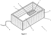
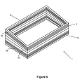
図1を参照すると、本発明の実施形態によるIPTシステムのための送信機1が示されている。送信機は、側壁3及び底部4を伴う充電筐体2の形式をとる。送信機は、筐体の内部に時変の磁界を生成するコイル5を含む。筐体の内部に置かれた機器6は、時変の磁界と誘導結合してその機器への充電と電力の供給のために用いられうる電流を生成する受信機コイル7を含む。コイルは、図1における破線によって示されるように、筐体の側壁に含まれると共に、底部と共通する面において筐体の外周に巻かれる。
(Coil configuration)
Referring to FIG. 1, a
送信機1は、適切な電源8に接続され、コイルが磁界を生成するようにそのコイルを駆動するように駆動回路(不図示)が構成される。駆動回路は、コイル5が特定の用途に適切な時変の磁界を生成するように構成される。このような駆動回路は、当業者に知られており、本発明は、この事項に限定されない。
The
誘導性で伝送された電力を受信することができる機器は、技術的に周知であり、本発明は、任意の特定の種類に限定されない。好ましい実施形態において、機器は、底部と同一平面の受信機コイルを含んでおり、これは、このことによって磁界の束がその底部と垂直である場合に電力伝送が最大化されるからである。 Equipment capable of receiving inductively transmitted power is well known in the art and the invention is not limited to any particular type. In a preferred embodiment, the instrument includes a receiver coil that is flush with the bottom because this maximizes power transfer when the flux of the magnetic field is perpendicular to the bottom.
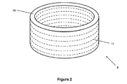
図1に示される筐体2の形状は、底面が長方形の角柱の形状をとるが、しかしながら本発明はこの事項に限られない。当業者は、筐体を定める様々な3次元の体積(volume)に適用するために、どのように本発明を作ることができるかを理解するだろう。例として、図2は、筐体が単一の連続した側壁10を有する円筒形上のものである送信機9を示している。この例では、コイル11は、図2における破線によって示されるように、大まかに円形であり、筐体の外周の周りに巻かれる。
The shape of the
本発明の好ましい実施形態において、筐体は、底部4を含む。後述するように、(フェライト層などの)磁気透過層を底部に含めることによって、電力伝送を大幅に改善することができる。しかしながら、必ずしも筐体2が底部を含む必要はない。当業者は、底部を含まない充電筐体に対してどのように本発明が適合されうるかを理解するだろう。
In a preferred embodiment of the present invention, the housing includes a
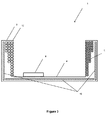
図3を参照すると、図1に示される送信機1の縦断面図が示されている。この図は、側壁3、底部4、コイル5、及び機器6を示している。筐体は、オプションとして、より魅力的かつ流線型の外観を送信機に与える、送信機の内部構造を取り囲む適切な外部層12(例えばプラスチックのハウジング)を含むことができる。コイルは、(単位高さごとのループの数である)コイルの密度が大まかに高さと共に増加するように構成される。これにより、側壁の最上部に向けて、より多くのループが「集中」する結果となる。図3に示されるループの数は、本発明の原理を図解するのに最も助けとなるため、相対的に少ない。現実には、ループの数は、いずれの事項にも限定されず、当業者は、ある用途において、ループの数が数百又は数千までもありうることを理解するだろう。
Referring to FIG. 3, a longitudinal sectional view of the
代わりに、本発明の別の実施形態では、その密度がある他の方式で高さと共に変動するようにコイルが構成されうる。例えば、コイルの密度が高さに伴って初期的には増加し、その後に側壁の最上部へ向けて再度減少することは本発明と調和する。このような代替の実施形態については後述する。 Alternatively, in another embodiment of the invention, the coil can be configured such that its density varies with height in other ways. For example, it is consistent with the present invention that the coil density initially increases with height and then decreases again towards the top of the sidewall. Such alternative embodiments are described below.
コイル5は、連続しており、駆動回路(不図示)に直列で接続される。本発明の実施形態において、コイルは、一連のループを形成するように繰り返し巻き回される単一の長さのワイヤからなる。本発明の1つの実施形態において、その単一の長さのワイヤは、ゲージを変動させるワイヤの区分を含む。そのワイヤの区分は、ワイヤの長さが最も大きい直径から最も狭い直径に徐々に変化するような適切な方法(例えばハンダ付けで)互いに接続されうる。このように、図3に示されるコイル構成に従ってワイヤが巻かれる場合、ワイヤの最も狭い区分が最も密度の高いループに対応する。ワイヤが最も狭いため、ワイヤが一貫したゲージを有する場合よりも占有するスペースが小さくなる。ワイヤは、Litzタイプのワイヤを含んだ、任意の適切な通電ワイヤでありうる。Litzワイヤは、IPTシステムにおいて高い周波数で動作される場合の導体における表皮効果及び近接効果に起因する電力損失を大幅に減らすため、有益である。本発明の別の実施形態において、1つより多くのコイルがある。各コイルは、直列に、並列に、又は他の適切な構成において接続されうる。全体に、(単位高さあたりのループの数である)コイルの正味の密度は、本発明に従ってなおも変動しうる。
The
本発明の利点を、本発明の実施形態による送信機1の縦断面図を示す図4a及び図4bにおいてみることができる。図4a及び図4bは、一様の密度を有するコイル構成と本発明によるコイル構成とによってそれぞれ生成される磁界の間の比較を図解している。図4aにおける前者のシナリオに対して、磁束が筐体13の壁に向かって集中し、中心14に向けて磁束が低い領域が存在することが観測される。ゆえに、この中心領域に置かれた受信機への十分な電力伝送を確実にするために、送信機を通る電力潮流を増加しなければならない。これは、供給電力の非効率な使用をもたらす。さらに、筐体の側壁により近く置かれた受信機は、中心に置かれたものより強い磁界を受ける。これは、受信機が、筐体の内部の正確な位置に応じてその電力潮流を調整することを要求する。また、機器内の寄生性の熱が増える。図4bは、本発明のコイル構成に従う磁界を明示する。観測されるように、可変コイル密度が、筐体を渡る、より一様の磁界をもたらす。効果的に、追加の巻き線は、磁界を筐体の内部にさらに伸ばす。これは、上述の非一様な場から生じる問題を解決するのに役立つ。特に、筐体の内部のその位置によらず、受信機への十分な電力伝送を確実にしながら、送信機を通る電力潮流を減らすことができる。送信機における電力潮流を減らしたことが、非効率性を最小化し、寄生性の熱を減少させる。当業者は、図4bに示される場が、本発明の原理を明示するための定性的なものであることを理解するだろう。実際には、所望の場の特性を得るために必要な正確なコイル構成は、寸法や出力定格などの多くの変数に依存する。コイル構成の設計は特定の用途に適合するように調整される必要があることが理解されるだろう。
The advantages of the present invention can be seen in FIGS. 4a and 4b showing longitudinal sections of a
図3に戻り、充電筐体の側壁3及び底部4の内部にフェライト層15も示されている。当業者は、どのように磁気透過層を含める事によって電力伝送の性能を改善することができるかを理解するだろう。具体的には、底部における磁気透過層は、中央により近くに磁力線を「強制的に」分布させる。これは、全体の底部領域にわたって、より一様な場を提供し、電力伝送を改善するのに役立つ。
Returning to FIG. 3, the
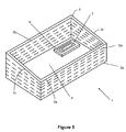
図5を参照すると、本発明の他の態様による送信機1を示している。この例において、送信機は、先に述べた充電筐体2と同様の充電筐体2であるが、充電筐体2aは、図1の実施形態におけるように底面が長方形の角柱形状ではない不規則な形状を有する。すなわち、筐体は、側壁3及び底部4を含み、接続する側壁3cが傾斜した上面を有するように側壁3aの1つが反対側の側壁3bと異なるサイズである。用語、上部及び下部は、底部4との関係において用いられる。筐体2aの実際の形状は、送信機の特定用途に依存するが、本発明との関係でここで説明されるコイル及び透過性物質の構成は、筐体が不規則に形成される状況に適用可能であることが理解されるべきである。
Referring to FIG. 5, a
後述するように、底部において(フェライト層などの)磁気透過層を含めることは、電力伝送を大幅に改善することができる。しかしながら、図1の実施形態のように、必ずしも筐体2aが底部を含まなくてもよい。当業者は、底部を含まない充電筐体に本発明がどのように適合されうるかを理解するだろう。
As described below, including a magnetically transmissive layer (such as a ferrite layer) at the bottom can greatly improve power transfer. However, as in the embodiment of FIG. 1, the
図5の破線で示されるように、筐体2aの内部で時変の磁界を生成するコイル5が、筐体の側壁に含まれ、筐体の外周に底部と同一平面において巻かれる。筐体2aの不規則な形状は、実質的に一様の方式で筐体の内部のすべてを実質的に取り囲む磁界を生成する一方で、不規則な形状に順応するコイル5の巻き構成を要求する。図5に図解するように、これは、コイル5の巻き線が筐体2aの少なくとも上部における側壁部3a、3b及び3cの上面に従うことを確実にすることにより、そして、上述の変動する密度のコイル構成を用いることによって、達成される。したがって、筐体2aの内部に置かれ、受信機コイル7を含んだ機器6は、筐体の内部の機器の相対的な位置取りによらず、その機器の充電又は電力供給を可能とするための時変の磁界と誘導結合する。
As shown by a broken line in FIG. 5, a
送信機1は適切な電源に接続され、駆動回路(不図示)は、コイルが磁界を生成するようにそのコイルを駆動するように構成される。駆動回路は、コイル5が特定の用途に適切な時変の磁界を生成するように構成される。このような駆動回路は当業者に知られており、本発明はこの事項に限定されない。
The
送信機コイルによって引き起こされる磁界の一様性のさらなる高度化が、図5の送信機1を示す、図6において図解されるようなコイル構成を用いて達成されうる。図6において、コイル5は、説明を補助するために、実践で図解される。図から分かるように、コイル5の巻き線構成は、すでに述べたように筐体2aの不規則形状に順応するが、図1および図5の実施形態において描画されるものと異なる、変化する(単位高さあたりのループの数である)密度構成が用いられる。すなわち、コイルの巻き線の密度が底部4から側壁3の上面へ単調増加する先の実施形態と異なり、図6の実施形態におけるコイルの巻き線の密度が側壁3の下部及び上部の両方において増加し、側壁の中間部において減少する。すなわち、筐体の上部における部分5a及び筐体の下部における部分5bの巻き線が、筐体の中間部における部分5cの巻き線よりより密に配置される。これは、側壁の最上部及び最下部に向けて、より多くのループが「集中する」結果をもたらす。図6に示されるループの数は、これが本発明の原理を図解するために最も役立つため、相対的に少ない。現実には、任意の事項においてループの数は限定されず、当業者は、いくつかの用途において、ループの数が数百又は数千でさえありうることを理解するだろう。本発明者は、この代替のコイル巻き線構成が、誘起される磁界におけるさらに良好な一様性を提供することを発見した。また、この構成は、筐体の内部の要求される場を供給しながら、筐体形状、寸法及び構成における不規則性を順応させることを可能とする。
Further enhancement of the uniformity of the magnetic field caused by the transmitter coil can be achieved using a coil configuration as illustrated in FIG. 6, showing the
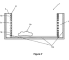
図7を参照すると、図6に示された送信機1の縦断面図が示されている。この図は、側壁3、底部4、コイル5、及び機器6aを示している。筐体は、オプションとして、送信機の内部構造を取り囲む適切な外部層12(例えばプラスチックのハウジング)を含むことができる。外部層12は、送信機1自身のための枠であってもよいし、車室又は他のインフラストラクチャのコンポーネントの一部であってもよい。機器6aは、先の図面において図解された一般的な矩形の機器の品物ではなく、任意の形状の品物として図解されている。任意の形状の機器6aは、本発明の様々な実施形態の送信機により誘起される磁界の一様性が、機器における受信機コイルの形状と送信機コイルに対する相対的な配向性との少なくともいずれかによらずに、効果的な無線の又は誘導性の電力伝送が実現されるようなものであることを図解するのに用いられている。
Referring to FIG. 7, a longitudinal sectional view of the
図5及び図6のコイル5は連続であり、駆動回路(不図示)に接続されうる。1つの実施形態において、コイルは、図7に示されるように、側壁の下部及び上部でのコイル部分5a及び5bにおいて互いに近接し、さらに、側壁の中間部でのコイル部分5cにおいて離れるループを有する、一連のループを形成するように繰り返し巻き回される単一の長さのワイヤである。別の実施形態では、コイル5は、図8に示されるように、変動するゲージのワイヤの区分を有しうる。すなわち、側壁の最高位又は最低位における区分5dは、側壁の中間部の区分5fより太い隣接区分5eより太い。これらのワイヤの区分は、ワイヤの長さが最も大きい直径から最も狭い直径に、さらに、側壁の高さにわたって最大の直径まで徐々に変化するような適切な方法(例えばハンダ付けで)互いに接続されうる。ワイヤは、Litzタイプのワイヤを含んだ、任意の適切な通電ワイヤでありうる。本発明の別の実施形態では、1つより多くのコイルがある。各コイルは、直列に、並列に、又は他の適切な構成で接続されうる。全体に、(単位高さあたりのループの数である)コイルの正味の密度は、本発明に従ってなおも変動しうる。
5 and 6 are continuous and can be connected to a drive circuit (not shown). In one embodiment, the coil has a loop that is close to each other in
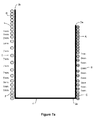
発明者は、図7に図解されるコイル構成を用いて、所定数のループ又は巻き数、密度が増加する部分5a及び5bにおける隣接する巻き間の間隔、及び増加された密度部分から減少した密度部分までの所定の漸次的変化が、誘起される磁界の最適化された操作を与えることを発見した。図7aは、図5及び図6に描画される規則的でない構成を伴う筐体を有する送信機の例示の実施形態を、同様の参照番号を用いて示している。図7aの例において、筐体2aの底部4からの高さに伴って増加から減少してそして増加するコイルの密度の漸次的変化を伴う、21巻きのコイル5が提供されており、漸次的変化は筐体2aの局所的な構成に依存している。すなわち、図から分かるように、筐体の「より高い」側の漸次的変化は筐体の「より低い」側における漸次的変化と異なる。
The inventor uses the coil configuration illustrated in FIG. 7 to determine a predetermined number of loops or turns, the spacing between adjacent turns in the
特に、この例において、低い方の側壁3aの筐体2aの開口(例えば、充電「箱」の最上部、ここで最上部は底部と相対的に定義される)に最も近いコイル5の部分Aは、最も高いコイル密度の10巻きを有し、ここで、隣接するコイルの巻きは互いに接触し、すなわち、隣接する巻き間に実質的なスペースはなく、その一方で、高い方の側壁3bの筐体2aの開口に最も近いコイル5の部分Dは、最も高いコイル密度の7巻きを有し、ここでコイルの隣接する巻きは互いに接触している。より低い側において、この隣接するコイルの巻き間の間隔は、1巻きに対して約1.0mmに増加し、一方で、より高い側ではその間隔は2巻きに対して約1.0mmに増加する。漸次的変化は、低い側及び高い側の両側で1巻きに対して隣接するコイルの巻き間で約3.0mmに、その後に両側で1巻きに対して約5.0mmに、間隔の増加を継続する。
In particular, in this example, the portion A of the
低い側での囲まれた体積(例えば、充電「箱」)の中間部分におけるコイルの部分Bでは、最小のコイル密度の3巻きが与えられ、ここでは、コイルの隣接する巻きは約6.0mm離れており、その一方で高い側の中間部分におけるコイル5の部分Eでは、最小のコイル密度の5巻きが与えられ、ここではコイルの隣接する巻きは約7.0mm離れている。漸次的変化は、低い側及び高い側の両方において、1巻きに対してコイルの隣接する巻き間で約5.0mm、その後に1巻きに対して約3.0mmに、その後に2つの巻きに対して約1.0mmに間隔の減少を継続する。最終的に、低い方の側壁3a及び高い方の側壁3bでの筐体2aの底部4に最も近いコイル5の部分C及びFは、それぞれ、最も高いコイルの密度のそれぞれの3巻きを有し、ここではコイルの隣接する巻きが互いに接触し、すなわち、隣接する巻き間に実質的にスペースがない。
The portion B of the coil in the middle portion of the lower enclosed volume (eg, charging “box”) is provided with a minimum coil density of 3 turns, where the adjacent turns of the coil are about 6.0 mm. Separately, while part E of the
この構成は、筐体の底部からの距離に応じた約0.0mmから約7.0mmまでの隣接する巻き間の20個の別個の間隔を伴う全21巻きを与える。理解されるように、相対的な間隔は、例えば、図6に描画されるように、筐体の「傾斜した」側面で持続する。 This configuration provides a total of 21 turns with 20 distinct spacings between adjacent turns from about 0.0 mm to about 7.0 mm depending on the distance from the bottom of the housing. As will be appreciated, the relative spacing persists on the “tilted” side of the housing, for example as depicted in FIG.
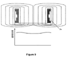
本発明の提示される実施形態の利得は、図8のコイル構成を有する送信機1の縦断面図とそれを用いて生成される磁界とを示す図9で見ることができる。図9のコイル構成によって生成される磁界を図4aで描画されるコイル構成によって生成されるものと比較すると、中央14に向けてのより低い磁束の領域を伴う磁束が筐体13の壁に向けて集中する図4aでの例と異なり、本実施形態の構成では、磁束が筐体2aの内部にわたってより一様であることを見ることができる。効果的に、追加の巻き線が、筐体内にさらに磁界を伸ばす。これは、先に議論した図4aの非一様な場から生じる問題を解決するのに役立つ。具体的には、本発明の送信機を通る電力潮流を、筐体の内部におけるその配置によらずに受信機に対する十分な電力伝送をなおも確実にしながら、図4aのそれに対して減らすことができる。送信機における電力潮流を減らしたことにより、非効率性が最小化され、寄生的な熱が低減される。当業者は、本発明の原理を明示するために図9に示される磁界が定性的であるということを理解するだろう。実際には、所望の場の特性を達成するのに必要な正確なコイル構成は、寸法や出力定格などの多くの変数に依存する。コイル構成の設計は特定の用途に適するように調整される必要があることが理解されるだろう。
The gain of the presented embodiment of the present invention can be seen in FIG. 9, which shows a longitudinal section of a
図7及び図8に戻り、筐体2aの側壁3及び底部4の内部の磁気透過性の要素材料15aが示されている。当業者は、フェライトなどの磁気透過性の材料を含めることがどのように電力伝送の性能を改善することができるかを理解するだろう。具体的には、適切な磁気透過性の材料が、中心の近くに磁力線を「強制的に」分布させる。これは、より一様な場を提供するとともに全体の底部領域にわたる電力伝送を改善するのに役立つ。また、送信機の筐体の外部の(電)磁界の生成を阻止し又はシールドする。これは、送信機の安全性と車室などの他の電子的な又は金属の構成部品を有する環境における送信機の使用の適合性を増進する。このシールド効果は、図7及び図8に図解されるように、要素15a間にギャップがないことを確実にすることによって、強化される。さらなる強化は、図8に図解されるように、側壁の上面の領域における送信機コイル5を覆う磁気透過性の要素材料のさらなる部分15bを与えることによって、提供されうる。磁気透過性の材料の、可動の蓋又はこの材料を有することも、提供されうる。効果的なシールドは、図3の実施形態そして後述される実施形態における要素15の構成によっても与えられる。なお、筐体の形状/構成と図1における接続部8などの電力接続とを収納するために、磁気透過性の要素材料がその部分を形成する枠におけるギャップを送信機のある用途が要求しうる。ギャップが回避されうる又は必要な用途のいずれにおいても、磁気透過性の要素材料は、当業者に周知のモールディング又は他の技術によって、別個の要素ではなく単一のユニットとして形成されうる。
Returning to FIG. 7 and FIG. 8, the magnetically
上述の充電/電力供給筐体は、独立の装置である必要はなく、既存の又は特別に設計された構造内に組み込まれてもよい。例として、机の引き出しが、本発明に従って構成されてもよく、したがって、ユーザは、その電子機器を引き出しに置くだけが必要となり、それらは充電され又は電力供給されうる。さらなる例において、車室のコンソールまたは他の同様の要素は、本発明にしたがう送信機筐体を組み込むように構成されてもよく、したがって、ユーザは、車のコンソールまたは同様の要素に電子機器を置くだけが必要となり、それによりその機器の充電又は電力供給が可能となる。 The charging / power supply enclosure described above need not be a separate device, but may be incorporated into an existing or specially designed structure. By way of example, desk drawers may be configured in accordance with the present invention so that the user only needs to place the electronic device in the drawer and they can be charged or powered. In a further example, a passenger compartment console or other similar element may be configured to incorporate a transmitter housing in accordance with the present invention, thus allowing a user to attach electronics to a car console or similar element. It only needs to be placed so that the device can be charged or powered.
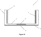
(磁気透過層−可変の厚さ)
図10を参照すると、本発明の別の態様による送信機1の断面図が示されている。この例において、送信機は、先の実施形態に関して説明された充電筐体2と同様の充電筐体である。筐体は、側壁3及び筐体の外周の周りに巻かれたコイル5を含み、すべては、適切な外部層12の内部に収納される。底部4に含まれるものは、メインの磁気透過層16である。上述のように、磁気透過層を含めることは、本質的に磁界を「再形成」することにより、電力伝送を改善することができる。このメインの磁気透過層に加えて、そのメインの磁気透過層に隣接して置かれる追加の磁気透過層17がある。
(Magnetic transmission layer-variable thickness)
Referring to FIG. 10, a cross-sectional view of a
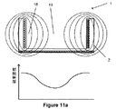
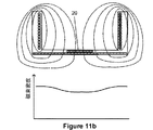
追加の磁気透過層17を含めた結果は、充電筐体2の中心に向かって磁気透過層の効果的な厚さを増やすこととなる。図10に示される本発明の実施形態において、これは、さらに充電筐体の中心に向かって磁界を強制することによって電力伝送を改善するのに役に立ち、より一様の磁界をもたらす。これは、図11a及び図11bに示されるように、磁力線の比較により明示される。図11aの前者のシナリオに対して筐体18の壁に向けて磁束が集中しており中心19に向けてより磁束が低い領域が存在していることが観測される。これは、先の図4aに関して説明されたものと同じ問題を生じさせる。図11bは、本発明の磁気透過層の構成に従う磁界を明示している。観測されるように、筐体2の中心20に向けて磁気透過層の厚さが増加することは、より一様の磁界をもたらす。これが生じる仕組みは、追加の磁気透過層を含めることが磁気透過層の高さを生じさせ、これが、筐体の中心を通る力線に対して、空間を通る磁路をより短くすることである。事実上、磁界は、中心に向かって「引き付けられ」る。同等に、より厚い磁気透過層は、より長い減少した磁気抵抗の区間を伴う磁路を与え、ゆえに、磁界がこの領域に向かうことが強制される。より一様な磁界は、先の図4aに関して説明されたような非一様の場から生じする問題を解決するのに役立つ。
The result of including the additional
図10を再度参照すると、追加のブロック17を含めることによって、磁気透過層の効果的な厚さの増加が達成されることがわかる。当業者は、追加のブロックの相対的なサイズは特定の送信機の規模及び寸法に依存することを理解するだろう。また、当業者は、一部の用途において、互いの上に徐々に減るサイズの一連の(すなわち3つ以上の)追加のブロックを積み重ねること、その結果「階段ピラミッド」タイプの構成となること、ここで、実効的な厚さが一連の離散的な段階で変動することが適切でありうることを理解するだろう。
Referring back to FIG. 10, it can be seen that the inclusion of the
本発明の代替の実施形態において、磁気透過層は、可変の厚さを伴って当初に製造されうる。この例において、厚さの変化は、(「階段ピラミッド」構成におけるような)離散で、又は連続でありうる。当業者は、磁気透過層における可変の厚さを達成するための他の可能な解決策があり、本発明がこの項目に限定されないことを理解するだろう。 In an alternative embodiment of the present invention, the magnetically permeable layer can be initially manufactured with a variable thickness. In this example, the change in thickness can be discrete (such as in a “stair pyramid” configuration) or continuous. One skilled in the art will appreciate that there are other possible solutions to achieve a variable thickness in the magnetically transmissive layer, and the present invention is not limited to this item.
本発明の別の実施形態では、磁気透過層の厚さが、別の方式で変わってもよく、必ずしも磁気透過層の中心に向かって増加しなくてもよい。例えば、いくつかの用途では、特定の送信機の端部に向かってより厚い磁気透過層を有することが有益でありうる。 In another embodiment of the present invention, the thickness of the magnetically transmissive layer may vary in other ways and does not necessarily increase toward the center of the magnetically transmissive layer. For example, in some applications it may be beneficial to have a thicker magnetically permeable layer towards the end of a particular transmitter.
本発明の好ましい実施形態では、磁気透過層はフェライト材料である。しかしながら、当業者は、他の適切な材料が同一の又は同様の効果のために用いられうることを理解するだろう。 In a preferred embodiment of the invention, the magnetically permeable layer is a ferrite material. However, those skilled in the art will appreciate that other suitable materials can be used for the same or similar effects.
本発明について充電筐体の底部に関して説明したが、本発明はこの用途に限定されない。当業者は、送信機に磁気透過層を含めることが有用な任意の場合において、本発明に従ってその層の厚さを変えることが可能であり、実際に価値がありうることを理解するだろう。例として、充電面であって、その面と共通の面において大きいコイルを含んだ充電面が、その面の中心に向かって厚さを増す磁気透過層を含めることによって益を得うる。これは、このような充電面の中心に向かって磁界がより弱くなること(及び電力伝送の効率が低くなること)に関連する問題を解決するのに役立つだろう。 Although the present invention has been described with respect to the bottom of the charging housing, the present invention is not limited to this application. Those skilled in the art will appreciate that in any case where it is useful to include a magnetically transmissive layer in the transmitter, it is possible to vary the thickness of that layer in accordance with the present invention and in fact be valuable. As an example, a charging surface that includes a large coil in a plane common to the surface may benefit from including a magnetically permeable layer that increases in thickness toward the center of the surface. This will help to solve the problems associated with a weaker magnetic field (and less efficient power transfer) towards the center of such a charging surface.
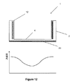
(磁気透過層−可変透磁率)
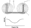
図12を参照すると、本発明の別の態様による、送信機1の断面図が示されている。この例では、送信機は、先に述べたその充電筐体と同様の充電筐体2である。筐体は、側壁3、及び筐体の外周に巻かれすべてが適切な外部層12の中に収納されたコイル5を含む。底部4に含まれるものは、磁気透過層20である。先に述べたように、磁気透過層を含めることは、磁界を本質的に「再形成」することにより、電力伝送を改善することができる。
(Magnetic transmission layer-variable permeability)
Referring to FIG. 12, a cross-sectional view of a
図12における対応するグラフに示されるように、磁気透過層20の透磁率は、充電筐体2の幅にわたって変動し、充電筐体の中心に向かっておおまかに最大となる透磁率を有する。図12に示される発明の実施形態では、充電筐体の中心に向かってさらに磁界を強制し、より一様な磁界をもたらすことにより電力伝送を改善するのに役立つ。図13a及び図13bに示されるように磁力線の比較によってこれが明示される。図13aの前者のシナリオに対して、磁束が筐体21の壁に向けて集中し、中心22に向かって磁束が低い領域が存在することが観測される。これは、先の図4aに関して説明されたものと同じ問題を生じさせる。図13bは、本発明の磁気透過層構成による磁界を明示している。観測されるように、筐体の中心に向かって磁気透過層の透磁率が増すことが、より一様な磁界をもたらす。これを生じさせる仕組みは、中心に向かって磁気透過層の透磁率を増加させ、磁気抵抗が減少した区間を伴う磁路をもたらし、したがって、この領域に磁界を強制することである。より一様な磁界は、先の図4aに関して説明したように、非一様な場から生じる問題を解決するのに役立つ。
As shown in the corresponding graph in FIG. 12, the magnetic permeability of the
再度、図12を参照すると、磁気透過層20が一定の厚さではあるが、連続的に透磁率が変化することがわかる。本発明の1つの実施形態において、磁気透過層は、その透磁率の特性のこのような連続的な変化を伴って当初に製造されうる。別の実施形態では、磁気透過層は、その透磁率特性の離散的な変動を伴って当初に製造されうる。
Referring again to FIG. 12, it can be seen that the
図14を参照すると、底部4の内部に互いに隣接して配置される磁気透過層23のいくつかの区分を含んだ、本発明による送信機1の別の実施形態が示されている。この例では、各区分の透磁率は、異なる大きさを有してもよく、これは、添付のグラフに示される透磁率の変動をもたらす。本発明の1つの実施形態による筐体の場合、このような区分は、磁気透過性の材料の同心円状の輪でできてもよい。
Referring to FIG. 14, another embodiment of the
本発明の別の実施形態では、磁気透過層の透磁率は、別の方式で変動してもよく、必ずしも磁気透過層の中心に向かって増える必要はない。例えば、ある用途において、特定の送信機の端部に向かってより高い透磁率を伴う磁気透過層を有することが有益でありうる。 In another embodiment of the present invention, the magnetic permeability of the magnetically transmissive layer may vary in other ways and does not necessarily increase toward the center of the magnetically permeable layer. For example, in certain applications, it may be beneficial to have a magnetically permeable layer with higher permeability towards the end of a particular transmitter.
本発明の好ましい実施形態では、磁気透過層はフェライト材料である。しかしながら、当業者は、同一の又は同様の効果のために他の適切な材料が用いられてもよい。 In a preferred embodiment of the invention, the magnetically permeable layer is a ferrite material. However, those skilled in the art may use other suitable materials for the same or similar effects.
本発明について充電筐体の底部に関して説明したが、本発明はこの用途に限定されない。当業者は、送信機に磁気透過層を含めることが有益な任意の場合に、本発明に従ってその層の透磁率を変動させることが可能でありうるし、実際に価値がありうることを理解するだろう。例として、充電面であって、その面と共通の面において大きいコイルを含んだ充電面が、その面の中心に向かって透磁率を増す磁気透過層を含めることによって益を得うる。これは、このような充電面の中心に向かって磁界がより弱くなること(及び電力伝送の効率が低くなること)に関連する問題を解決するのに役立つだろう。 Although the present invention has been described with respect to the bottom of the charging housing, the present invention is not limited to this application. Those skilled in the art will understand that in any case where it is beneficial to include a magnetically transmissive layer in the transmitter, it may be possible to vary the permeability of that layer in accordance with the present invention and may actually be valuable. Let's go. By way of example, a charging surface that includes a large coil in a plane common to the surface may benefit from including a magnetically permeable layer that increases the permeability toward the center of the surface. This will help to solve the problems associated with a weaker magnetic field (and less efficient power transfer) towards the center of such a charging surface.
(組み合わせ)
本発明による送信機のいくつかの態様、すなわち:可変のコイル密度;磁気透過層の可変の厚さ;及び磁気透過層の可変の透磁率、について説明してきた。当業者は、いくつもの方法で、これらの態様の任意のものが組み合わされうることを理解するだろう。例えば、ある充電筐体に対して、筐体の最上部に向けて増加するコイル密度と、底部の中央に向けて透磁率が増加する磁気透過層を含んだ底部と、を有する価値がありうる。別の例では、充電面が、磁気透過層を含んでもよく、ここで、その層の厚さと透磁率とがその充電面の中央に向けて次第に増加しうる。磁気透過性の材料を含む本発明の任意の実施形態では、材料「層」又は「シールド」が、約1.0mmより薄い、例えば0.5mmの厚さを有しうる。さらに、透磁率は、北川工業製のフェライトDS037803のものでありうる。
(combination)
Several aspects of the transmitter according to the present invention have been described: variable coil density; variable thickness of magnetic transmission layer; and variable permeability of magnetic transmission layer. Those skilled in the art will appreciate that any of these aspects can be combined in a number of ways. For example, for a charging case, it may be worth having a coil density that increases towards the top of the case and a bottom that includes a magnetically permeable layer that increases the permeability towards the center of the bottom. . In another example, the charging surface may include a magnetically permeable layer, where the thickness and permeability of the layer may gradually increase toward the center of the charging surface. In any embodiment of the invention that includes a magnetically permeable material, the material “layer” or “shield” may have a thickness of less than about 1.0 mm, for example 0.5 mm. Further, the magnetic permeability can be that of ferrite DS0378803 manufactured by Kitagawa Industries.
送信機コイルによる時変の磁界の生成を駆動するのに用いられる駆動回路は、図15に示すように、電流注入トポロジを有しうる。このトポロジでは、DC電源が、インバータ構成を用いて送信機コイルを横断する正弦曲線の電圧へと変換される。インバータは、2つの動作モード:電力注入及び自由振動を有する。スイッチSaが「閉じて」おりスイッチSbが「開いて」いる場合、インダクタL(例えば送信機コイル)と直列コンデンサCとによって与えられる共振タンクが、電源に直接接続される。この期間において、電力が共振タンクに注入される。その一方で、スイッチSaが「開いて」おりスイッチSbが「閉じて」いる場合、インダクタL、その同調コンデンサC、及びレジスタRが、自由振動網を形成する。共振タンクの閉路内に蓄積された電力は、コンデンサにおける電界とインダクタにおける磁界の形式で振動する。スイッチの制御は、マイクロコントローラなどの適切な制御回路によって与えられる。送信機が車室に提供される本発明の用途において、DC電源は12Vの電源でありうる。他の用途は、AC電源を要求しうるが、当業者であればそれをどのように実装するかを理解するだろう。 The drive circuit used to drive the generation of the time-varying magnetic field by the transmitter coil can have a current injection topology, as shown in FIG. In this topology, a DC power source is converted to a sinusoidal voltage across the transmitter coil using an inverter configuration. The inverter has two modes of operation: power injection and free vibration. When switch Sa is “closed” and switch Sb is “open”, the resonant tank provided by inductor L (eg, transmitter coil) and series capacitor C is directly connected to the power source. During this period, power is injected into the resonant tank. On the other hand, when the switch Sa is “open” and the switch Sb is “closed”, the inductor L, its tuning capacitor C, and the resistor R form a free vibration network. The power stored in the closed tank tank oscillates in the form of an electric field in the capacitor and a magnetic field in the inductor. Control of the switch is provided by a suitable control circuit such as a microcontroller. In the application of the invention in which a transmitter is provided in the passenger compartment, the DC power source can be a 12V power source. Other applications may require an AC power source, but those skilled in the art will understand how to implement it.
このように、より一様な磁界の生成をもたらすIPTシステムのための送信機構成が提供される。磁界がより一様であるため、送信機と受信機との間の結合の品質が改善され、機器に電力を供給し又は充電するのに必要な電力がより低くなり、より効率的なIPTシステムをもたらす。さらに、機器に電力供給するために要求される電流が減るため、送信機の近くに又はその上に置かれた機器において、寄生的な熱による損失が小さくなる。 Thus, a transmitter configuration for an IPT system that provides more uniform magnetic field generation is provided. A more uniform IP field improves the quality of the coupling between the transmitter and the receiver, requires less power to power or charge the equipment, and is a more efficient IPT system Bring. In addition, since the current required to power the equipment is reduced, the loss due to parasitic heat is reduced in equipment located near or on the transmitter.
本発明についてその実施形態の説明によって図解したが、そして、その実施形態について詳細に説明したが、出願人は添付の請求項の範囲を、このような詳細に制限し、いかなる方法によっても限定することを意図していない。追加の利点及び変更は当業者にはすでに見えているだろう。したがって、より広範な態様における本発明が、特定の詳細、代表的な装置並びに方法、及び、示されて説明された図解例に限定されない。したがって、出願人の一般的な発明のコンセプトの精神又は範囲から離れることなく、このような詳細からの離脱が行われてもよい。 Although the present invention has been illustrated by description of its embodiments, and has been described in detail, the applicant has limited the scope of the appended claims to such details and limited in any way Not intended. Additional advantages and modifications will already be apparent to those skilled in the art. Accordingly, the invention in its broader aspects is not limited to the specific details, representative apparatus and methods, and illustrative examples shown and described. Accordingly, departures from such details may be made without departing from the spirit or scope of applicants' general inventive concept.
Claims (6)
b.前記筐体の内部において交流磁界を生成するための1つ以上のコイルであって、前記1つ以上のコイルの密度が初期的には前記底部からの距離の増加に伴って低下し、その後に前記底部からの距離のさらなる増加に伴って増加する、1つ以上のコイルと、
c.前記1つ以上のコイルを駆動するための駆動回路と、
を含む誘導性電力伝送送信機。 a. A housing having a bottom and one or more side walls projecting from the bottom, for housing to provide energy to the device;
b. One or more coils for generating an alternating magnetic field within the housing, wherein the density of the one or more coils initially decreases with increasing distance from the bottom, and thereafter One or more coils that increase with further increase in distance from the bottom;
c. A drive circuit for driving the one or more coils;
Including inductive power transmission transmitter.
請求項1に記載の誘導性電力伝送送信機。 The one or more coils are roughly wound to correspond to an outer periphery of the housing;
The inductive power transmission transmitter according to claim 1.
請求項1に記載の誘導性電力伝送送信機。 The housing has a plurality of side walls, one of the side walls being generally higher than the other side wall;
The inductive power transmission transmitter according to claim 1.
請求項2に記載の誘導性電力伝送送信機。 The housing includes one or more magnetically permeable elements associated with the one or more coils.
The inductive power transmission transmitter according to claim 2.
請求項2に記載の誘導性電力伝送送信機。 The change in density of the one or more coils is provided by constructing the one or more coils from wires having varying dimensions.
The inductive power transmission transmitter according to claim 2.
請求項1に記載の誘導性電力伝送送信機。 The one or more coils comprise a Litz wire;
The inductive power transmission transmitter according to claim 1.
Applications Claiming Priority (3)
| Application Number | Priority Date | Filing Date | Title |
|---|---|---|---|
| US201462055924P | 2014-09-26 | 2014-09-26 | |
| US62/055,924 | 2014-09-26 | ||
| PCT/NZ2015/050160 WO2016048170A1 (en) | 2014-09-26 | 2015-09-22 | Transmitter for inductive power transfer system |
Publications (2)
| Publication Number | Publication Date |
|---|---|
| JP2017530557A true JP2017530557A (en) | 2017-10-12 |
| JP2017530557A5 JP2017530557A5 (en) | 2018-10-11 |
Family
ID=55581550
Family Applications (1)
| Application Number | Title | Priority Date | Filing Date |
|---|---|---|---|
| JP2017516355A Pending JP2017530557A (en) | 2014-09-26 | 2015-09-22 | Transmitter for inductive power transmission system |
Country Status (6)
| Country | Link |
|---|---|
| US (1) | US10818430B2 (en) |
| EP (1) | EP3198620B1 (en) |
| JP (1) | JP2017530557A (en) |
| KR (1) | KR102210318B1 (en) |
| CN (1) | CN107077963B (en) |
| WO (1) | WO2016048170A1 (en) |
Cited By (1)
| Publication number | Priority date | Publication date | Assignee | Title |
|---|---|---|---|---|
| JP2019079870A (en) * | 2017-10-23 | 2019-05-23 | 国立大学法人信州大学 | Transmission coil component for non-contact power supply, method of manufacturing the same, and non-contact power supply device |
Families Citing this family (9)
| Publication number | Priority date | Publication date | Assignee | Title |
|---|---|---|---|---|
| US10231505B2 (en) | 2015-05-28 | 2019-03-19 | Nike, Inc. | Article of footwear and a charging system for an article of footwear |
| US10658847B2 (en) | 2015-08-07 | 2020-05-19 | Nucurrent, Inc. | Method of providing a single structure multi mode antenna for wireless power transmission using magnetic field coupling |
| US10063100B2 (en) | 2015-08-07 | 2018-08-28 | Nucurrent, Inc. | Electrical system incorporating a single structure multimode antenna for wireless power transmission using magnetic field coupling |
| US11205848B2 (en) | 2015-08-07 | 2021-12-21 | Nucurrent, Inc. | Method of providing a single structure multi mode antenna having a unitary body construction for wireless power transmission using magnetic field coupling |
| CN107786003A (en) * | 2016-08-24 | 2018-03-09 | 泰科电子(上海)有限公司 | Wireless power supply and electrical equipment |
| KR20190040993A (en) | 2016-08-24 | 2019-04-19 | 타이코 일렉트로닉스 (상하이) 컴퍼니 리미티드 | Wireless power supply devices and electrical devices |
| US10958105B2 (en) | 2017-02-13 | 2021-03-23 | Nucurrent, Inc. | Transmitting base with repeater |
| JP7200956B2 (en) * | 2020-01-27 | 2023-01-10 | 株式会社村田製作所 | inductor components |
| CN113300482A (en) * | 2021-04-29 | 2021-08-24 | 伏达半导体(合肥)有限公司 | Wireless power transmission apparatus, method and system |
Citations (6)
| Publication number | Priority date | Publication date | Assignee | Title |
|---|---|---|---|---|
| US20080246675A1 (en) * | 2005-07-22 | 2008-10-09 | Winstead Assets Limited | Field Winding |
| US20090303693A1 (en) * | 2008-06-09 | 2009-12-10 | Shau-Gang Mao | Wireless Power Transmitting Apparatus |
| JP2011517926A (en) * | 2008-03-13 | 2011-06-16 | アクセス ビジネス グループ インターナショナル リミテッド ライアビリティ カンパニー | Inductive charging system having a plurality of primary coils |
| JP2012134248A (en) * | 2010-12-20 | 2012-07-12 | Yazaki Corp | Resonance coil and non-contact power transmission device with resonance coil |
| US20130119927A1 (en) * | 2011-01-18 | 2013-05-16 | Mojo Mobility, Inc. | Methods for improved transfer efficiency in a multi-dimensional inductive charger |
| JP2014534623A (en) * | 2011-10-07 | 2014-12-18 | パワーバイプロキシ リミテッド | Inductive power transfer system transmitter |
Family Cites Families (37)
| Publication number | Priority date | Publication date | Assignee | Title |
|---|---|---|---|---|
| US3800213A (en) | 1972-10-24 | 1974-03-26 | Develco | Three axis toroidal fluxgate type magnetic sensor |
| US4825166A (en) | 1987-01-27 | 1989-04-25 | Sundstrand Data Control, Inc. | Bobbin for a magnetic sensor |
| JPH04317527A (en) | 1991-04-15 | 1992-11-09 | Matsushita Electric Works Ltd | Noncontact charger for rechargeable electric appliance |
| US5281941A (en) | 1991-08-14 | 1994-01-25 | Elliot Bernstein | Coil form and coil for antenna coils, or the like |
| DE69631799T2 (en) | 1995-05-29 | 2004-07-29 | Matsushita Electric Industrial Co., Ltd., Kadoma | POWER UNIT |
| JP2001190029A (en) | 1999-12-28 | 2001-07-10 | Matsushita Electric Ind Co Ltd | Charger |
| ATE270771T1 (en) | 2000-03-09 | 2004-07-15 | Abb Research Ltd | ARRANGEMENT FOR GENERATING ELECTRICAL ENERGY FROM A MAGNETIC FIELD |
| DE10218124B4 (en) | 2002-04-23 | 2004-07-15 | Siemens Ag | Charger for contactless charging of battery-operated devices |
| WO2003096361A1 (en) | 2002-05-13 | 2003-11-20 | Splashpower Limited | Improvements relating to the transfer of electromagnetic power |
| GB0210886D0 (en) | 2002-05-13 | 2002-06-19 | Zap Wireless Technologies Ltd | Improvements relating to contact-less power transfer |
| GB2388716B (en) | 2002-05-13 | 2004-10-20 | Splashpower Ltd | Improvements relating to contact-less power transfer |
| US7414380B2 (en) | 2004-09-21 | 2008-08-19 | Lear Corporation | Apparatus for inductively recharging batteries of a portable convenience device |
| US20080000522A1 (en) * | 2006-06-30 | 2008-01-03 | General Electric Company | Photovoltaic device which includes all-back-contact configuration; and related processes |
| WO2008026080A2 (en) | 2006-09-01 | 2008-03-06 | Bio Aim Technologies Holding Ltd. | Systems and methods for wireless power transfer |
| JP4209437B2 (en) | 2006-11-10 | 2009-01-14 | 三菱重工業株式会社 | Non-contact power feeding device for mobile body and protection device therefor |
| KR100937627B1 (en) * | 2007-04-30 | 2010-01-19 | (주)제이씨 프로텍 | Non-Directional Charging Device and Wireless Charging Set of Small Electronic Device |
| US20090010462A1 (en) | 2007-07-02 | 2009-01-08 | Front Edge Technology, Inc. | Compact rechargeable thin film battery system for hearing aid |
| GB0716679D0 (en) | 2007-08-28 | 2007-10-03 | Fells J | Inductive power supply |
| JP2009089452A (en) | 2007-09-27 | 2009-04-23 | Denso Corp | Charging system |
| JP5363720B2 (en) | 2007-11-15 | 2013-12-11 | リコーエレメックス株式会社 | Non-contact transfer device and transfer core |
| US20090201142A1 (en) * | 2008-02-07 | 2009-08-13 | The Texas A&M University System | Wireless Sensor System |
| US7456606B1 (en) | 2008-04-23 | 2008-11-25 | International Business Machines Corporation | Battery label with wireless battery charging circuit |
| JP2010041906A (en) | 2008-07-10 | 2010-02-18 | Nec Tokin Corp | Contactless power transmission apparatus, soft magnetic sheet, and module using the same |
| EP2161811A1 (en) | 2008-09-05 | 2010-03-10 | Koninklijke Philips Electronics N.V. | Inductive charger and charging method |
| US8587155B2 (en) | 2008-09-27 | 2013-11-19 | Witricity Corporation | Wireless energy transfer using repeater resonators |
| US8487480B1 (en) | 2008-09-27 | 2013-07-16 | Witricity Corporation | Wireless energy transfer resonator kit |
| US9530555B2 (en) * | 2011-03-29 | 2016-12-27 | Triune Systems, LLC | Wireless power transmittal |
| WO2010127685A1 (en) | 2009-05-07 | 2010-11-11 | Telecom Italia S.P.A. | System for transferring energy wirelessly |
| US8460816B2 (en) | 2009-10-08 | 2013-06-11 | Etymotic Research, Inc. | Rechargeable battery assemblies and methods of constructing rechargeable battery assemblies |
| US20110115429A1 (en) | 2009-11-13 | 2011-05-19 | Nokia Corporation | Wireless Charging Adapter Compatible With Wall Charger And Wireless Charging Plate |
| US8390249B2 (en) | 2009-11-30 | 2013-03-05 | Broadcom Corporation | Battery with integrated wireless power receiver and/or RFID |
| JP2013533607A (en) | 2010-05-28 | 2013-08-22 | コーニンクレッカ フィリップス エヌ ヴェ | Improved receiver coil |
| WO2013179284A2 (en) * | 2012-05-29 | 2013-12-05 | Humavox Ltd. | Wireless charging device |
| EP2878062A4 (en) * | 2012-07-27 | 2016-04-20 | Thoratec Corp | Resonant power transmission coils and systems |
| WO2014018976A1 (en) | 2012-07-27 | 2014-01-30 | H. Lee Moffitt Cancer Center And Research Institute, Inc. | Multi-spectral fluorescence for in-vivo determination of proton energy and range in proton therapy |
| WO2014145664A1 (en) * | 2013-03-15 | 2014-09-18 | Thoratec Corporation | Integrated implantable tets housing including fins and coil loops |
| US9780573B2 (en) * | 2014-02-03 | 2017-10-03 | Witricity Corporation | Wirelessly charged battery system |
-
2015
- 2015-09-22 KR KR1020177011271A patent/KR102210318B1/en active IP Right Grant
- 2015-09-22 CN CN201580051926.6A patent/CN107077963B/en active Active
- 2015-09-22 US US15/514,251 patent/US10818430B2/en active Active
- 2015-09-22 EP EP15844230.1A patent/EP3198620B1/en active Active
- 2015-09-22 JP JP2017516355A patent/JP2017530557A/en active Pending
- 2015-09-22 WO PCT/NZ2015/050160 patent/WO2016048170A1/en active Application Filing
Patent Citations (6)
| Publication number | Priority date | Publication date | Assignee | Title |
|---|---|---|---|---|
| US20080246675A1 (en) * | 2005-07-22 | 2008-10-09 | Winstead Assets Limited | Field Winding |
| JP2011517926A (en) * | 2008-03-13 | 2011-06-16 | アクセス ビジネス グループ インターナショナル リミテッド ライアビリティ カンパニー | Inductive charging system having a plurality of primary coils |
| US20090303693A1 (en) * | 2008-06-09 | 2009-12-10 | Shau-Gang Mao | Wireless Power Transmitting Apparatus |
| JP2012134248A (en) * | 2010-12-20 | 2012-07-12 | Yazaki Corp | Resonance coil and non-contact power transmission device with resonance coil |
| US20130119927A1 (en) * | 2011-01-18 | 2013-05-16 | Mojo Mobility, Inc. | Methods for improved transfer efficiency in a multi-dimensional inductive charger |
| JP2014534623A (en) * | 2011-10-07 | 2014-12-18 | パワーバイプロキシ リミテッド | Inductive power transfer system transmitter |
Cited By (2)
| Publication number | Priority date | Publication date | Assignee | Title |
|---|---|---|---|---|
| JP2019079870A (en) * | 2017-10-23 | 2019-05-23 | 国立大学法人信州大学 | Transmission coil component for non-contact power supply, method of manufacturing the same, and non-contact power supply device |
| JP7082785B2 (en) | 2017-10-23 | 2022-06-09 | 国立大学法人信州大学 | Transmission coil parts for non-contact power supply, their manufacturing method, and non-contact power supply equipment |
Also Published As
| Publication number | Publication date |
|---|---|
| US10818430B2 (en) | 2020-10-27 |
| WO2016048170A1 (en) | 2016-03-31 |
| CN107077963A (en) | 2017-08-18 |
| EP3198620B1 (en) | 2021-04-07 |
| CN107077963B (en) | 2021-08-06 |
| EP3198620A4 (en) | 2017-11-01 |
| US20170301462A1 (en) | 2017-10-19 |
| KR102210318B1 (en) | 2021-02-01 |
| KR20170063825A (en) | 2017-06-08 |
| EP3198620A1 (en) | 2017-08-02 |
Similar Documents
| Publication | Publication Date | Title |
|---|---|---|
| JP6081469B2 (en) | Inductive power transfer system transmitter | |
| JP2017530557A (en) | Transmitter for inductive power transmission system | |
| RU2534020C1 (en) | Wireless charging system for mobile devices | |
| JP4356844B2 (en) | Non-contact power feeding device | |
| US20110304217A1 (en) | Non-contact power feeding device | |
| US9680311B2 (en) | Wireless power supply system | |
| US10566853B2 (en) | Inductive power transmitter | |
| US11251661B2 (en) | Inductive power transmitter | |
| JP2020099193A (en) | Wireless charging system with solenoid | |
| JP5592242B2 (en) | Power receiving device, power transmitting device, and wireless power transmission system | |
| JP2017524324A (en) | Wireless power transfer through metal objects | |
| JP2011045189A (en) | Method and device for shielding electromagnetic wave in radio power transmission system, and radio power transmission device | |
| JP2015509282A (en) | Inductive wireless charging system | |
| JP6486456B2 (en) | Wireless charging of electronic devices with metal back | |
| JP2014187724A (en) | Secondary power-receiving apparatus and charging stand and secondary power-receiving apparatus | |
| JP2019501614A (en) | Coupled resonator in metal back cover | |
| JP2014039437A (en) | Charge and discharge device | |
| US10305330B2 (en) | Power transmission device | |
| JP2015015417A (en) | Power transmitting or power receiving device | |
| JP2016012614A (en) | Coil unit and power supply system |
Legal Events
| Date | Code | Title | Description |
|---|---|---|---|
| A711 | Notification of change in applicant |
Free format text: JAPANESE INTERMEDIATE CODE: A711 Effective date: 20180227 |
|
| A521 | Request for written amendment filed |
Free format text: JAPANESE INTERMEDIATE CODE: A523 Effective date: 20180903 |
|
| A621 | Written request for application examination |
Free format text: JAPANESE INTERMEDIATE CODE: A621 Effective date: 20180903 |
|
| A977 | Report on retrieval |
Free format text: JAPANESE INTERMEDIATE CODE: A971007 Effective date: 20190524 |
|
| A131 | Notification of reasons for refusal |
Free format text: JAPANESE INTERMEDIATE CODE: A131 Effective date: 20190603 |
|
| A02 | Decision of refusal |
Free format text: JAPANESE INTERMEDIATE CODE: A02 Effective date: 20200106 |