JP2017148109A - Optical interference tomography apparatus - Google Patents

Optical interference tomography apparatus Download PDF

Info

Publication number
JP2017148109A
JP2017148109A JP2016030836A JP2016030836A JP2017148109A JP 2017148109 A JP2017148109 A JP 2017148109A JP 2016030836 A JP2016030836 A JP 2016030836A JP 2016030836 A JP2016030836 A JP 2016030836A JP 2017148109 A JP2017148109 A JP 2017148109A
Authority
JP
Japan
Prior art keywords
light
light source
optical
unit
frequency
Prior art date
Legal status (The legal status is an assumption and is not a legal conclusion. Google has not performed a legal analysis and makes no representation as to the accuracy of the status listed.)
Granted
Application number
JP2016030836A
Other languages
Japanese (ja)
Other versions
JP6679340B2 (en
Inventor
藤井 英一
Hidekazu Fujii
英一 藤井
Current Assignee (The listed assignees may be inaccurate. Google has not performed a legal analysis and makes no representation or warranty as to the accuracy of the list.)
Canon Inc
Original Assignee
Canon Inc
Priority date (The priority date is an assumption and is not a legal conclusion. Google has not performed a legal analysis and makes no representation as to the accuracy of the date listed.)
Filing date
Publication date
Application filed by Canon Inc filed Critical Canon Inc
Priority to JP2016030836A priority Critical patent/JP6679340B2/en
Publication of JP2017148109A publication Critical patent/JP2017148109A/en
Application granted granted Critical
Publication of JP6679340B2 publication Critical patent/JP6679340B2/en
Active legal-status Critical Current
Anticipated expiration legal-status Critical

Links

Images

Abstract

PROBLEM TO BE SOLVED: To provide an optical interference tomography apparatus capable of suppressing deterioration of an SNR of an image due to amplitude fluctuation of a MEMS minute vibration mirror in a frequency sweeping light source.SOLUTION: An optical interference tomography apparatus includes: a light source part that sweeps a frequency of an emitted light; an interference part for dividing the light emitted from the light source part into an irradiation light to be irradiated onto the ocular fundus of a subject and a reference light, and generating an interference light by the reflection light of the irradiation light from the ocular fundus and the reference light; a scanning part for scanning the ocular fundus with the irradiation light; a detection part for detecting the interference light; an information acquisition part for acquiring the information on the ocular fundus based on the interference light; an optical filter part for reflecting or transmitting a light of a specific frequency of the light emitted from the light source part; and a light detection device for receiving the reflected light or the transmitted light from the optical filter part and generating a detection signal. The light source part includes a light source having a MEMS device used for frequency sweeping of the light emitted from the light source part, and a control part for controlling the light output of the light source part using the detection signal.SELECTED DRAWING: Figure 1

Description

本発明は、光干渉断層計に関する。   The present invention relates to an optical coherence tomography.

光干渉断層計(Optical Coherence Tomography:OCT又はOCT装置)が開発されている。OCT装置は、干渉の技術を用いた光によって非侵襲に被検体の断層像に関する情報を取得することができる。OCT装置は、様々な分野で利用されているが、特に非侵襲に被検体の断層像を観察できるため、医療分野にて非常に有用である。特に眼科領域においては外部からの観察が主な診断方法であるため、急速にOCT装置の普及が進んでいる。   An optical coherence tomography (OCT or OCT apparatus) has been developed. The OCT apparatus can acquire information on a tomographic image of a subject non-invasively by light using interference technology. The OCT apparatus is used in various fields, but is particularly useful in the medical field because it can observe a tomographic image of a subject non-invasively. In particular, in the ophthalmologic field, observation from the outside is the main diagnostic method, and therefore the OCT apparatus is rapidly spreading.

OCTには、大きく分けてタイムドメインOCT(Time Domain OCT)及びフーリエドメインOCT(Fourier Domain OCT)と呼ばれる二つの方式がある。さらにフーリエドメインOCTの中でも、スペクトラルドメインOCT(Spectral Domain OCT:SD−OCT)、スウェプトソースOCT(Swept Source OCT:SS−OCT)の2つの方式が知られている。   OCT is roughly divided into two methods called time domain OCT (Time Domain OCT) and Fourier domain OCT (Fourier Domain OCT). Further, among Fourier domain OCT, two methods of Spectral Domain OCT (Spectral Domain OCT: SD-OCT) and Swept Source OCT (Swept Source OCT: SS-OCT) are known.

SS−OCTでは、時間的に波長を広帯域に変化させる光源を用い、サンプル光と参照光とで干渉させた光の強度を各々の波長で取得する。SS−OCTでは、この波長に対する干渉フリンジに対しフーリエ解析を行い、光軸上にある奥行き方向における被検体の反射面の位置の情報を算出し、算出した情報に基づいて被検体の断層画像を構成することができる。SS−OCTは高速に断層像を取得できるため、精力的に開発がすすめられている技術である。   In SS-OCT, a light source that changes the wavelength in a wide band with time is used, and the intensity of the light caused to interfere with the sample light and the reference light is acquired at each wavelength. In SS-OCT, Fourier analysis is performed on the interference fringe for this wavelength, information on the position of the reflecting surface of the subject in the depth direction on the optical axis is calculated, and a tomographic image of the subject is calculated based on the calculated information. Can be configured. Since SS-OCT can acquire tomographic images at high speed, it is a technology that has been energetically developed.

SS−OCTでは出力波長を広帯域に掃引可能な波長掃引光源(周波数掃引光源)を使用する。波長掃引光源は様々な方式のものが開発されているが、SS−OCT用の光源としてはMEMS(Micro Electronic Mechanical Systems)波長選択フィルタを用いたものが多く使用されている。これは、SS−OCTで必要な40nmを超える広帯域を、波長掃引周波数100kHz以上といった高速で波長(周波数)掃引するために、MEMS波長選択フィルタを用いた光源が適しているためである。   SS-OCT uses a wavelength swept light source (frequency swept light source) that can sweep the output wavelength over a wide band. Although various types of wavelength swept light sources have been developed, many light sources using SS (OCT) wavelength selective filters are used as light sources for SS-OCT. This is because a light source using a MEMS wavelength selective filter is suitable for sweeping a wavelength (frequency) at a high speed such as a wavelength sweep frequency of 100 kHz or more in a wide band exceeding 40 nm necessary for SS-OCT.

MEMS波長選択フィルタを用いた波長掃引光源には、MEMSのファブリペローフィルタを用いた外部共振器型の波長掃引光源やMEMSのチルトミラーを用いた外部共振器型波長掃引光源、MEMS‐VCSELと呼ばれる波長掃引光源等がある。ここで、MEMS‐VCSEL(Vertical Cavity Surface Emitting Laser)はVCSELとMEMS可動ミラーを組み合わせた光源である。   The wavelength swept light source using the MEMS wavelength selection filter is called an external resonator type wavelength swept light source using a MEMS Fabry-Perot filter, an external resonator type wavelength swept light source using a MEMS tilt mirror, and called MEMS-VCSEL. There is a wavelength swept light source. Here, a MEMS-VCSEL (Vertical Cavity Surface Emitting Laser) is a light source that combines a VCSEL and a MEMS movable mirror.

MEMS波長選択フィルタを用いた波長掃引光源は、MEMSの微小振動ミラー(以下、MEMS微小振動ミラーという。)の往復運動を利用して波長選択を行い、波長掃引光を出力している。MEMS微小振動ミラーは代表的なMEMSデバイスの一つであり、ビームスキャナーなど、波長掃引光源以外にも広く利用されている。   A wavelength swept light source using a MEMS wavelength selection filter performs wavelength selection using a reciprocating motion of a MEMS micro-vibration mirror (hereinafter referred to as a MEMS micro-vibration mirror), and outputs a wavelength swept light. The MEMS micro-vibration mirror is one of typical MEMS devices, and is widely used in addition to a wavelength swept light source such as a beam scanner.

しかし、MEMS微小振動ミラーは、温度や気圧の変化によりその振動振幅が変動するという問題を有している。MEMS微小振動ミラーを波長掃引に利用した波長掃引光源の場合、MEMS微小振動ミラーの振動振幅が変動すると掃引する波長範囲(波長掃引幅)が変動してしまう。   However, the MEMS micro-vibration mirror has a problem that the vibration amplitude fluctuates due to changes in temperature and atmospheric pressure. In the case of a wavelength swept light source using a MEMS micro-vibration mirror for wavelength sweeping, if the vibration amplitude of the MEMS micro-vibration mirror varies, the wavelength range (wavelength sweep width) to be swept varies.

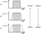
MEMS微小振動ミラーを波長掃引に利用した波長掃引光源において、温度や気圧が変化した場合に波長掃引幅が変化する様子の一例を図2に示す。図2には、気圧が高い又は温度が低い場合の波長掃引幅を示すグラフ201、気圧及び温度が中程度の場合の波長掃引幅を示すグラフ202、並びに気圧が低い又は温度が高い場合の波長掃引幅を示すグラフ203を示されている。なお、グラフ201,202,203において、ハッチングされた部分は、波長掃引幅が最も狭くなった場合(グラフ201に示す場合)に掃引する波長範囲を示す。   FIG. 2 shows an example of how the wavelength sweep width changes when the temperature or atmospheric pressure changes in a wavelength swept light source that uses a MEMS micro-vibration mirror for wavelength sweeping. FIG. 2 is a graph 201 showing the wavelength sweep width when the atmospheric pressure is high or the temperature is low, the graph 202 showing the wavelength sweep width when the atmospheric pressure and the temperature are medium, and the wavelength when the atmospheric pressure is low or the temperature is high. A graph 203 showing the sweep width is shown. In the graphs 201, 202, and 203, hatched portions indicate the wavelength ranges to be swept when the wavelength sweep width becomes the narrowest (shown in the graph 201).

MEMS微小振動ミラーは、気圧が高い又は温度が低いと振動振幅が減少し、気圧が低い又は温度が高いと振動振幅が増大する。そのため、MEMS微小振動ミラーを用いた波長掃引光源の波長掃引幅は、気圧や温度の変化により、図2に示すように、気温が高い又は温度が低いと狭く、気温が低い又は温度が高いと広くなるように変化してしまう。   In the MEMS micro-vibration mirror, the vibration amplitude decreases when the atmospheric pressure is high or the temperature is low, and the vibration amplitude increases when the atmospheric pressure is low or the temperature is high. Therefore, as shown in FIG. 2, the wavelength sweep width of the wavelength sweep light source using the MEMS micro-vibration mirror is narrow when the temperature is high or low, and the temperature is low or high, as shown in FIG. It will change to become wider.

ところで、SS−OCTでは、画像形成に用いる干渉信号の波長幅で断層像の深さ分解能が決まる。ここで、画像形成など、断層に関する情報取得に用いる干渉信号の波長幅は、光源から出射される光の波長幅に依存する。MEMS微小振動ミラーを用いた波長掃引光源では、上述のように気圧や温度に応じて波長掃引幅が変化してしまうため、このような波長掃引光源をSS−OCTに用いると、気圧や温度などの環境によって、得られる断層像の深さ分解能が変化してしまう。   By the way, in SS-OCT, the depth resolution of a tomographic image is determined by the wavelength width of an interference signal used for image formation. Here, the wavelength width of the interference signal used for acquiring information about the tomography such as image formation depends on the wavelength width of the light emitted from the light source. In the wavelength sweep light source using the MEMS micro-vibration mirror, the wavelength sweep width changes according to the atmospheric pressure and temperature as described above. Therefore, when such a wavelength sweep light source is used for SS-OCT, the atmospheric pressure, the temperature, etc. Depending on the environment, the depth resolution of the obtained tomographic image changes.

撮像した時の環境や装置の状態によって、得られる断層像の深さ分解能が変化しにくいことが、医療機器として好ましい。そこで、OCT装置、特に眼底用のOCT装置では、画像形成に使用する光の波長範囲をあらかじめ設計の段階で決めてしまうことが一般的である。   It is preferable for a medical device that the depth resolution of an obtained tomographic image hardly changes depending on the environment at the time of imaging and the state of the apparatus. Therefore, in an OCT apparatus, particularly a fundus OCT apparatus, the wavelength range of light used for image formation is generally determined in advance at the design stage.

従って、そのようなOCT装置において、図2に示したように波長掃引光源の波長掃引幅が変動する場合には、波長掃引幅が最も狭くなる場合を想定して、図2に斜線でハッチングした波長範囲の光のみを画像形成に使用する。つまり、グラフ202やグラフ203のように波長掃引幅が広くなっている場合は、ハッチングされていない部分の波長の光が、画像形成に利用されない無駄な光として瞳内に入射することになる。眼底用のOCTでは、網膜へダメージを与えないために、瞳入射光量が厳しく制限されている。そのため、眼底用のOCTでは、画像形成に寄与しない無駄な光が瞳内に入射すると、その分画像形成に使える光量が減少することになり、画像のSNR(signal−to−noise ratio)が低下する。また、被検体が目以外においても、入射光量の制限がある測定対象であれば、画像のSNR低下という課題は生じうる。そのため、このようなMEMS微小振動ミラーの振動振幅の変動に起因する画像のSNRの低下を抑制する眼底用のOCT装置が望まれている。   Therefore, in such an OCT apparatus, when the wavelength sweep width of the wavelength swept light source fluctuates as shown in FIG. 2, it is hatched with diagonal lines in FIG. 2 assuming that the wavelength sweep width is the narrowest. Only light in the wavelength range is used for image formation. That is, when the wavelength sweep width is wide as in the graph 202 and the graph 203, the light having the wavelength that is not hatched enters the pupil as wasted light that is not used for image formation. In OCT for the fundus, the amount of incident light on the pupil is severely limited in order not to damage the retina. Therefore, in the fundus OCT, when useless light that does not contribute to image formation enters the pupil, the amount of light that can be used for image formation decreases, and the SNR (signal-to-noise ratio) of the image decreases. To do. Even if the subject is other than the eye, if the measurement target is limited in the amount of incident light, the problem of a reduction in the SNR of the image may occur. Therefore, there is a demand for an OCT apparatus for the fundus that suppresses a decrease in the SNR of an image caused by such fluctuations in the vibration amplitude of the MEMS microvibration mirror.

特許文献1に記載の技術では、波長掃引におけるデータの取り込みタイミングを当該波長掃引において生成されたトリガ信号により決定し、安定したデータの取り込みを可能にする光干渉断層像形成装置が記載されている。   The technique described in Patent Document 1 describes an optical coherence tomographic image forming apparatus that determines the data acquisition timing in the wavelength sweep by the trigger signal generated in the wavelength sweep and enables stable data acquisition. .

特開2012−239514号公報JP 2012-239514 A

しかし、特許文献1の光干渉断層像形成装置では、画像形成に用いない範囲の波長の光についての制御がなされていないため、上述の画像のSNRが低下する、という課題が生じうる。   However, since the optical coherence tomographic image forming apparatus disclosed in Patent Document 1 does not control light in a wavelength range not used for image formation, there is a problem that the SNR of the above-described image is reduced.

そこで、本発明は、周波数掃引光源におけるMEMS微小振動ミラーの振幅変動による画像のSNRの低下を抑制することができる光干渉断層計を提供する。   Accordingly, the present invention provides an optical coherence tomometer that can suppress a decrease in the SNR of an image due to amplitude fluctuation of a MEMS micro-vibration mirror in a frequency swept light source.

本発明の一実施態様によれば、射出する光の周波数を掃引する光源部と、前記光源部から射出された光を被検体の眼底へ照射する照射光と参照光に分割し、前記眼底からの前記照射光の反射光と前記参照光による干渉光を発生させる干渉部と、前記眼底を前記照射光で走査する走査部と、前記干渉光を検出する検出部と、前記検出部によって検出された前記干渉光に基づいて、前記眼底の情報を取得する情報取得部と、前記光源部から射出された光のうち特定の周波数の光を反射又は透過する光学フィルタ部と、前記光学フィルタ部からの反射光又は透過光を受光して検出信号を生成する光検出装置とを備え、前記光源部は、前記光源部から射出される光の周波数掃引に用いられるMEMSデバイスを有する光源と、前記検出信号を用いて、前記光源部の光出力を制御する制御部とを含む、光干渉断層計が提供される。   According to one embodiment of the present invention, the light source unit that sweeps the frequency of the emitted light, and the light emitted from the light source unit is divided into irradiation light and reference light that irradiates the fundus of the subject, and from the fundus Detected by the detection unit, a scanning unit that scans the fundus with the irradiation light, a detection unit that detects the interference light, and an interference unit that generates interference light by the reflected light of the irradiation light and the reference light. Based on the interference light, an information acquisition unit that acquires information on the fundus oculi, an optical filter unit that reflects or transmits light of a specific frequency among the light emitted from the light source unit, and the optical filter unit And a light detection device that generates a detection signal by receiving reflected or transmitted light of the light source, the light source unit having a MEMS device used for frequency sweeping of light emitted from the light source unit, and the detection Using the signal And a control unit for controlling the light output of the serial light source unit, an optical coherence tomography is provided.

本発明によれば、周波数掃引光源におけるMEMS微小振動ミラーの振幅変動による画像のSNRの低下を抑制することができる。   ADVANTAGE OF THE INVENTION According to this invention, the fall of SNR of the image by the amplitude fluctuation | variation of the MEMS micro oscillating mirror in a frequency sweep light source can be suppressed.

本発明の一実施形態による光干渉断層計の概略的な構成を示す。1 shows a schematic configuration of an optical coherence tomography according to an embodiment of the present invention. MEMSデバイスを用いた波長掃引光源の波長掃引幅に対する環境の影響を説明するための図である。It is a figure for demonstrating the influence of the environment with respect to the wavelength sweep width | variety of the wavelength sweep light source using a MEMS device. 本発明の一実施形態に係る断層像のSNRを改善するプロセスを説明するための図である。It is a figure for demonstrating the process which improves SNR of the tomogram which concerns on one Embodiment of this invention. 本発明の実施例1に係るMEMS‐VCSEL光源の概略的な構成を示す。1 shows a schematic configuration of a MEMS-VCSEL light source according to Embodiment 1 of the present invention. 本発明の実施例1に係る光源部の概略的な構成を示す。1 shows a schematic configuration of a light source unit according to Embodiment 1 of the present invention. 本発明の実施例1による光干渉断層計の作用を説明するための図である。It is a figure for demonstrating the effect | action of the optical coherence tomography by Example 1 of this invention. 本発明の実施例2による光干渉断層計の概略的な構成を示す。The schematic structure of the optical coherence tomography by Example 2 of this invention is shown. 本発明の実施例3に係る光源部の概略的な構成を示す。6 shows a schematic configuration of a light source unit according to Example 3 of the present invention. 本発明の実施例3に係る断層像のSNRを改善するプロセスを説明するための図である。It is a figure for demonstrating the process which improves the SNR of the tomogram based on Example 3 of this invention.

以下に、本発明を実施するための例示的な実施形態及び実施例を、図面を参照して詳細に説明する。図面において、同一であるか又は機能的に類似している要素を示すために図面間で同じ参照符号を用い、重複する説明は省略する。ただし、以下の実施形態及び実施例で説明する寸法、材料、形状、構成要素の相対的な位置等は任意であり、本発明が適用される装置の構成又は様々な条件に応じて変更できる。   Hereinafter, exemplary embodiments and examples for carrying out the present invention will be described in detail with reference to the drawings. In the drawings, the same reference numerals are used in the drawings to denote the same or functionally similar elements, and redundant description is omitted. However, dimensions, materials, shapes, relative positions of components, and the like described in the following embodiments and examples are arbitrary, and can be changed according to the configuration of the apparatus to which the present invention is applied or various conditions.

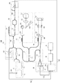
以下、図1を参照して本発明の一実施形態による光干渉断層計について述べる。なお、以下において、本実施形態による光干渉断層計として眼底用のOCT装置について述べる。図1は、本実施形態におけるOCT装置100の概略的な構成例を示す。   Hereinafter, an optical coherence tomography according to an embodiment of the present invention will be described with reference to FIG. In the following, the OCT apparatus for the fundus will be described as the optical coherence tomograph according to the present embodiment. FIG. 1 shows a schematic configuration example of an OCT apparatus 100 in the present embodiment.

OCT装置100には、射出する光の周波数を掃引する光源部10と、干渉光を生成する干渉部20と、干渉光を検出する検出部30と、干渉光に基づいて、被検体156の眼底の情報を取得する情報取得部40と、表示部70とが設けられている。また、OCT装置100には、被検体156に照射光を照射し、被検体156からの反射光を干渉部20へ出射する測定アーム50と、測定アーム50から出射される反射光と干渉させる参照光を干渉部20へ出射する参照アーム60とが設けられている。さらに、OCT装置100には、検出部30における干渉信号のサンプリングタイミングを示すkクロック信号184を生成するkクロック生成部80と、所定の周波数の光を検出し、光周波数検出信号193を生成する光周波数検出部90とが設けられている。   The OCT apparatus 100 includes a light source unit 10 that sweeps the frequency of emitted light, an interference unit 20 that generates interference light, a detection unit 30 that detects interference light, and the fundus of the subject 156 based on the interference light. The information acquisition part 40 which acquires the information of this, and the display part 70 are provided. Further, the OCT apparatus 100 irradiates the subject 156 with irradiation light, and emits the reflected light from the subject 156 to the interference unit 20, and the reference for causing interference with the reflected light emitted from the measurement arm 50. A reference arm 60 that emits light to the interference unit 20 is provided. Furthermore, the OCT apparatus 100 detects a light having a predetermined frequency by generating a k clock signal 184 indicating the sampling timing of the interference signal in the detection unit 30, and generates an optical frequency detection signal 193. An optical frequency detector 90 is provided.

光源部10には、光を射出するとともに、射出する光の周波数(波長)を掃引することができる周波数掃引光源111(光源)と、周波数掃引光源111を制御する光源部制御部112(制御部)が設けられている。周波数掃引光源111は、MEMS微小振動ミラー(MEMSデバイス)と光を発生するゲイン媒体を含む。周波数掃引光源111では、ゲイン媒体を駆動させることで光を発生させ、MEMS微小振動ミラーを駆動させることで、発生した光の周波数を掃引する。なお、光源部10では、ゲイン媒体の駆動を制御することで、光源部10の光出力のオンオフ切り替えが可能である。また、光源部制御部112は、周波数掃引光源内のMEMS微小振動ミラー及びゲイン媒体の駆動をそれぞれ制御することができる。光源部10の詳細な動作については後述する。   The light source unit 10 emits light and a frequency swept light source 111 (light source) that can sweep the frequency (wavelength) of the emitted light, and a light source unit control unit 112 (control unit) that controls the frequency swept light source 111. ) Is provided. The frequency sweep light source 111 includes a MEMS micro-vibration mirror (MEMS device) and a gain medium that generates light. The frequency sweep light source 111 generates light by driving the gain medium, and sweeps the frequency of the generated light by driving the MEMS micro-vibration mirror. In the light source unit 10, the light output of the light source unit 10 can be switched on and off by controlling the driving of the gain medium. In addition, the light source control unit 112 can control driving of the MEMS micro-vibration mirror and the gain medium in the frequency sweep light source. Detailed operation of the light source unit 10 will be described later.

光源部10から射出された光はカプラ101に入射し、カプラ101は、入射した光をカプラ102に入射する光と干渉部20に入射する光に分割する。カプラ102は、入射した光をkクロック生成部80に入射する光と光周波数検出部90に入射する光に分割する。   The light emitted from the light source unit 10 enters the coupler 101, and the coupler 101 divides the incident light into light incident on the coupler 102 and light incident on the interference unit 20. The coupler 102 divides the incident light into light incident on the k clock generation unit 80 and light incident on the optical frequency detection unit 90.

干渉部20には、カプラ121,122が設けられている。カプラ121は、光源部10から射出された光を眼底へ照射する照射光と参照光とに分割する。   Couplers 121 and 122 are provided in the interference unit 20. The coupler 121 divides the light emitted from the light source unit 10 into irradiation light for irradiating the fundus and reference light.

照射光は、測定アーム50を経由して被検体156に照射される。測定アーム50には、偏光コントローラ151と、コリメータ152と、X軸スキャナー153と、Y軸スキャナー154と、フォーカスレンズ155とが設けられている。偏光コントローラ151は、カプラ121から測定アーム50に接続される光ファイバーに設けられ、測定アーム50を通る照射光及び反射光の偏光状態を整える。コリメータ152は、光ファイバーを介してカプラ121と接続されている。   The irradiation light is applied to the subject 156 via the measurement arm 50. The measurement arm 50 is provided with a polarization controller 151, a collimator 152, an X-axis scanner 153, a Y-axis scanner 154, and a focus lens 155. The polarization controller 151 is provided in an optical fiber connected from the coupler 121 to the measurement arm 50 and adjusts the polarization state of the irradiation light and the reflected light passing through the measurement arm 50. The collimator 152 is connected to the coupler 121 via an optical fiber.

測定アーム50に入射した照射光は、偏光コントローラ151で偏光状態を整えられた後、コリメータ152から空間光として出射される。その後、照射光は、X軸スキャナー153、Y軸スキャナー154、及びフォーカスレンズ155を介して被検体156の眼底に照射される。   Irradiation light incident on the measurement arm 50 is adjusted in polarization state by the polarization controller 151 and then emitted from the collimator 152 as spatial light. Thereafter, the irradiation light is applied to the fundus of the subject 156 via the X-axis scanner 153, the Y-axis scanner 154, and the focus lens 155.

X軸スキャナー153及びY軸スキャナー154は、それぞれ回転軸が互いに直交するよう配置された偏向ミラーで構成されている。X軸スキャナー153及びY軸スキャナー154は眼底を照射光で走査する機能を有する走査部を構成し、眼底に対する照射光の照射位置を変更することができる。ここで、X軸スキャナー153はX軸方向の走査を行い、Y軸スキャナー154はY軸方向の走査を行う。なお、X軸方向、Y軸方向の各方向は、眼球の眼軸方向に対して垂直な方向で、互いに垂直な方向である。   The X-axis scanner 153 and the Y-axis scanner 154 are configured by deflection mirrors that are arranged so that their rotation axes are orthogonal to each other. The X-axis scanner 153 and the Y-axis scanner 154 constitute a scanning unit having a function of scanning the fundus with irradiation light, and can change the irradiation position of the irradiation light on the fundus. Here, the X-axis scanner 153 performs scanning in the X-axis direction, and the Y-axis scanner 154 performs scanning in the Y-axis direction. Note that the X-axis direction and the Y-axis direction are directions perpendicular to the eye axis direction of the eyeball and perpendicular to each other.

眼底に照射された照射光は、眼底において後方散乱光(反射光)として反射される。眼底からの反射光は、再びフォーカスレンズ155、Y軸スキャナー154、X軸スキャナー153、コリメータ152、偏光コントローラ151を経由して測定アーム50から出射される。そして、光ファイバー及びカプラ121を経由してカプラ122に入射する。   Irradiation light applied to the fundus is reflected as backscattered light (reflected light) on the fundus. The reflected light from the fundus is emitted from the measurement arm 50 via the focus lens 155, the Y-axis scanner 154, the X-axis scanner 153, the collimator 152, and the polarization controller 151 again. Then, the light enters the coupler 122 via the optical fiber and the coupler 121.

一方、参照光は参照アーム60を経由し、カプラ122に入射する。参照アーム60には、偏光コントローラ161と、コリメータ162と、分散補償ガラス163と、光路長調整光学系164と、分散調整プリズムペア165と、コリメータ166とが設けられている。偏光コントローラ161は、カプラ121から参照アーム60に接続される光ファイバーに設けられ、参照アーム60を通る参照光の偏光状態を整える。コリメータ162は、光ファイバーを介してカプラ121と接続されている。   On the other hand, the reference light enters the coupler 122 via the reference arm 60. The reference arm 60 is provided with a polarization controller 161, a collimator 162, a dispersion compensation glass 163, an optical path length adjustment optical system 164, a dispersion adjustment prism pair 165, and a collimator 166. The polarization controller 161 is provided in an optical fiber connected from the coupler 121 to the reference arm 60 and adjusts the polarization state of the reference light passing through the reference arm 60. The collimator 162 is connected to the coupler 121 via an optical fiber.

参照アーム60に入射した参照光は、偏光コントローラ161で偏光状態を整えられた後、コリメータ162から空間光として出射される。その後、参照光は分散補償ガラス163、光路長調整光学系164、及び分散調整プリズムペア165を通り、コリメータ166に入射する。   The reference light that has entered the reference arm 60 is adjusted in polarization state by the polarization controller 161 and then emitted from the collimator 162 as spatial light. Thereafter, the reference light passes through the dispersion compensation glass 163, the optical path length adjustment optical system 164, and the dispersion adjustment prism pair 165 and enters the collimator 166.

分散補償ガラス163及び分散調整プリズムペア165は、参照光の分散を調整することができる。そのため、分散補償ガラス163及び分散調整プリズムペア165を用いることで、測定アーム50を経由する反射光の分散に対応するように参照光の分散を調整することができる。また、光路長調整光学系164は、コリメータ162,166に対し近づく又は遠ざかる方向に移動することができ、参照アーム60の光路長を調整することができる。そのため、光路長調整光学系164によって、照射光が経由する被検体156の眼底までの光路長に応じて、参照アーム60の光路長を調整することができる。   The dispersion compensation glass 163 and the dispersion adjustment prism pair 165 can adjust the dispersion of the reference light. Therefore, by using the dispersion compensation glass 163 and the dispersion adjustment prism pair 165, the dispersion of the reference light can be adjusted so as to correspond to the dispersion of the reflected light passing through the measurement arm 50. The optical path length adjustment optical system 164 can move in a direction approaching or moving away from the collimators 162 and 166, and can adjust the optical path length of the reference arm 60. Therefore, the optical path length of the reference arm 60 can be adjusted by the optical path length adjustment optical system 164 according to the optical path length to the fundus of the subject 156 through which the irradiation light passes.

コリメータ166に入射した参照光は、コリメータ166を介して光ファイバーに入射され参照アーム60から出射される。そして、光ファイバーを経由して、カプラ122に入射する。   The reference light incident on the collimator 166 is incident on the optical fiber via the collimator 166 and is emitted from the reference arm 60. Then, the light enters the coupler 122 via the optical fiber.

カプラ122に入射した反射光と参照光は、互いに干渉し、互いに位相が反転した2つの干渉光がカプラ122から2つの光ファイバー内に出射され、検出部30に入射する。そして、検出部30は入射した干渉光を検出する。   The reflected light and the reference light incident on the coupler 122 interfere with each other, and two interference lights whose phases are inverted are emitted from the coupler 122 into the two optical fibers and are incident on the detection unit 30. And the detection part 30 detects the incident interference light.

検出部30には、差動検出器131とA/D変換器132が設けられている。差動検出器131は、カプラ122から2つの光ファイバーを経由して入射したそれぞれの干渉光を検出する。ここで、差動検出器131に入射する2つの干渉光は、互いに干渉信号成分の位相が反転しているため、差動検出器131で差動検出することにより良好なSN比で干渉信号成分を検出できる。   The detector 30 is provided with a differential detector 131 and an A / D converter 132. The differential detector 131 detects each interference light incident from the coupler 122 via two optical fibers. Here, since the phase of the interference signal component of the two interference lights incident on the differential detector 131 is inverted, the differential signal is detected by the differential detector 131 so that the interference signal component can be obtained with a good SN ratio. Can be detected.

差動検出器131は、検出した干渉光から電気信号に変換された干渉信号133をA/D変換器132に送り、A/D変換器132は受け取った干渉信号133をデジタル信号に変換する。なお、A/D変換器132にはkクロック生成部80が接続されており、A/D変換器132はkクロック生成部80から送られてくるkクロック信号184に同期して干渉信号133をサンプリングし、デジタル信号に変換する。さらに、A/D変換器132には光周波数検出部90が接続されており、A/D変換器132は光周波数検出部90から光周波数検出信号193を受け取る。A/D変換器132は、受け取った光周波数検出信号193に基づいて、サンプリングすべき波長範囲の干渉光に基づく干渉信号133を把握し、kクロック信号184に同期して当該干渉信号133をサンプリングする。A/D変換器132は、デジタル信号に変換した干渉信号を情報取得部40に送る。   The differential detector 131 sends an interference signal 133 converted from the detected interference light to an electrical signal to the A / D converter 132, and the A / D converter 132 converts the received interference signal 133 into a digital signal. The A / D converter 132 is connected to the k clock generation unit 80, and the A / D converter 132 outputs the interference signal 133 in synchronization with the k clock signal 184 sent from the k clock generation unit 80. Sample and convert to digital signal. Furthermore, the optical frequency detector 90 is connected to the A / D converter 132, and the A / D converter 132 receives the optical frequency detection signal 193 from the optical frequency detector 90. Based on the received optical frequency detection signal 193, the A / D converter 132 grasps the interference signal 133 based on the interference light in the wavelength range to be sampled, and samples the interference signal 133 in synchronization with the k clock signal 184. To do. The A / D converter 132 sends the interference signal converted into a digital signal to the information acquisition unit 40.

情報取得部40は、検出部30から受け取ったデジタル信号に対してフーリエ変換などの周波数分析を行い、被検体156の眼底の情報を得る。なお、情報取得部40は、差動検出器131で検出した干渉信号成分の位相が反転した干渉光に基づく干渉信号の差を取ることで、干渉信号の干渉成分を検出し、干渉信号の非干渉成分に基づくノイズを低減することができる。そのため、情報取得部40は、当該差動検出を行うことで、干渉信号に基づく眼底の情報の信号対雑音比(S/N比)を改善することができる。情報取得部40は、得られた眼底の情報を表示部70に送り、表示部70は受け取った情報を断層像として表示する。   The information acquisition unit 40 performs frequency analysis such as Fourier transform on the digital signal received from the detection unit 30 to obtain information on the fundus of the subject 156. The information acquisition unit 40 detects the interference component of the interference signal by taking the difference of the interference signal based on the interference light whose phase of the interference signal component detected by the differential detector 131 is inverted, and detects the non-interference signal. Noise based on the interference component can be reduced. Therefore, the information acquisition unit 40 can improve the signal-to-noise ratio (S / N ratio) of the fundus information based on the interference signal by performing the differential detection. The information acquisition unit 40 sends the obtained fundus information to the display unit 70, and the display unit 70 displays the received information as a tomographic image.

なお、情報取得部40は、CPUやMPUなどを備えた任意の情報処理部としてOCT装置100内に構成されてもよいし、汎用コンピュータを用いて構成されてもよい。また表示部70は、任意のモニターで構成されることができ、OCT装置100に備えつけられたモニターであってもよいし、OCT装置100に接続された個別のモニターであってもよい。また、本実施形態では、検出器として差動検出器131を用いているが、単に干渉光を検出し干渉信号を生成する検出器を用いてもよい。この場合、カプラ122から検出器に接続される光ファイバーは1つでよい。   Note that the information acquisition unit 40 may be configured in the OCT apparatus 100 as an arbitrary information processing unit including a CPU, an MPU, or the like, or may be configured using a general-purpose computer. In addition, the display unit 70 can be configured by an arbitrary monitor, and may be a monitor provided in the OCT apparatus 100 or an individual monitor connected to the OCT apparatus 100. In the present embodiment, the differential detector 131 is used as a detector. However, a detector that simply detects interference light and generates an interference signal may be used. In this case, only one optical fiber may be connected from the coupler 122 to the detector.

kクロック生成部80は、カプラ102を経由した光源部10から射出された光に基づいてkクロック信号184を生成し、検出部30に送る。kクロック生成部80には、カプラ181,182及び光検出部183が設けられている。   The k clock generation unit 80 generates a k clock signal 184 based on the light emitted from the light source unit 10 via the coupler 102 and sends the k clock signal 184 to the detection unit 30. The k clock generation unit 80 includes couplers 181 and 182 and a light detection unit 183.

kクロック生成部80に入射した光は、カプラ181によって光路長の異なる2つの光路に導波され、当該2つの光路を経由した光はカプラ182に入射して互いに干渉し、干渉光として光検出部183に入射する。光検出部183は入射した光を検出し、検出した干渉光に基づいてkクロック信号184を生成する。kクロック生成部80は生成したkクロック信号184を検出部30に送り、検出部30は干渉光の検出を行い、kクロック生成部80から受け取ったkクロック信号184と同期して干渉光に基づく干渉信号を生成する。   The light incident on the k clock generation unit 80 is guided to two optical paths having different optical path lengths by the coupler 181, and the lights passing through the two optical paths are incident on the coupler 182 and interfere with each other, and are detected as interference light. Incident on part 183. The light detection unit 183 detects the incident light and generates a k clock signal 184 based on the detected interference light. The k clock generation unit 80 sends the generated k clock signal 184 to the detection unit 30, and the detection unit 30 detects the interference light, and is based on the interference light in synchronization with the k clock signal 184 received from the k clock generation unit 80. Generate an interference signal.

光周波数検出部90は、カプラ102を経由した光源部10から射出された光に基づいて光周波数検出信号193(検出信号)を生成し、光源部10及び検出部30に送る。光周波数検出部90には、FBG(Fiber Bragg Grating:ファイバーブラッググレーティング)191及び光検出装置192が設けられている。   The optical frequency detection unit 90 generates an optical frequency detection signal 193 (detection signal) based on the light emitted from the light source unit 10 via the coupler 102 and sends it to the light source unit 10 and the detection unit 30. The optical frequency detection unit 90 is provided with an FBG (Fiber Bragg Grating) 191 and a light detection device 192.

FBG191(光学フィルタ部)は、特定の周波数(波長)の光を反射する。FBG191によって反射された光はカプラ102を経由して光検出装置192に入射する。光検出装置192は入射した光を検出し、光周波数検出信号193を生成する。光周波数検出部90は生成した光周波数検出信号193を検出部30に送り、検出部30は受け取った光周波数検出信号193に基づいて光源部10から発せられた光の波長掃引(周波数掃引)のタイミングを把握する。検出部30は、光周波数検出信号193に基づいて、被検体156の断層画像を形成するために用いられる波長範囲の干渉光に基づく干渉信号をサンプリングする。光周波数検出信号193に対する光源部10の動作は後述する。   The FBG 191 (optical filter unit) reflects light having a specific frequency (wavelength). The light reflected by the FBG 191 enters the light detection device 192 via the coupler 102. The light detection device 192 detects the incident light and generates an optical frequency detection signal 193. The optical frequency detection unit 90 sends the generated optical frequency detection signal 193 to the detection unit 30, and the detection unit 30 performs a wavelength sweep (frequency sweep) of the light emitted from the light source unit 10 based on the received optical frequency detection signal 193. Know the timing. Based on the optical frequency detection signal 193, the detection unit 30 samples an interference signal based on interference light in a wavelength range used for forming a tomographic image of the subject 156. The operation of the light source unit 10 with respect to the optical frequency detection signal 193 will be described later.

なお、本実施形態では、特定の周波数の光を反射する光学部材(光学フィルタ部)として、FBGを利用した。しかしながら、当該光学部材として、エタロン及び干渉フィルタ等の波長選択可能な他の部材を用いることもできる。また、光周波数検出部90は、特定の周波数の光を透過する部材を用い、透過光を検出する構成としても良い。   In the present embodiment, FBG is used as an optical member (optical filter unit) that reflects light of a specific frequency. However, other optically selectable members such as an etalon and an interference filter can be used as the optical member. The optical frequency detector 90 may be configured to detect transmitted light using a member that transmits light of a specific frequency.

また、図1のOCT装置100では、上述のように、干渉光のサンプリングは、光源部10の外に設けられるkクロック生成部80が発信するkクロック信号184に基づいて等光周波数(等波数)間隔に行われる。これに対し、kクロック生成部を光源部10に組み込んでもよい。   Further, in the OCT apparatus 100 of FIG. 1, as described above, the sampling of the interference light is performed based on the k optical signal (equal wave number) based on the k clock signal 184 transmitted from the k clock generation unit 80 provided outside the light source unit 10. ) Done at intervals. On the other hand, the k clock generation unit may be incorporated in the light source unit 10.

上記一連の動作により、OCT装置100は、被検体156のある1点における断層に関する情報を取得することができる。このように、被検体156の奥行き方向の断層に関する情報を取得することをA−スキャンと呼ぶ。また、OCT装置100では、X軸スキャナー153及びY軸スキャナー154によって構成される走査部によって、被検体156を走査することにより、被検体の2次元の断層像や3次元の断層像の情報を取得することができる。   Through the series of operations described above, the OCT apparatus 100 can acquire information regarding a tomogram at a certain point of the subject 156. Obtaining information related to the tomography in the depth direction of the subject 156 in this way is called an A-scan. In the OCT apparatus 100, the scanning unit configured by the X-axis scanner 153 and the Y-axis scanner 154 scans the subject 156, thereby obtaining information on a two-dimensional tomographic image and a three-dimensional tomographic image of the subject. Can be acquired.

ここで、A−スキャンと直交する方向における被検体156の断層に関する情報、すなわち2次元の断層像の情報を取得するための走査方向に被検体156を走査することをB−スキャンと呼ぶ。さらに、A−スキャン及びB−スキャンのいずれの走査方向とも直交する方向に被検体156を走査することをC−スキャンと呼ぶ。特に、3次元の断層像の情報を取得する際に被検体156の眼底面内に2次元ラスター走査する場合、高速に走査が行われる方向をB−スキャン方向と呼び、B−スキャン方向に直交し、低速に走査が行われる方向をC−スキャン方向と呼ぶ。   Here, scanning the subject 156 in the scanning direction for acquiring information on the tomographic image of the subject 156 in a direction orthogonal to the A-scan, that is, information on a two-dimensional tomographic image, is called a B-scan. Furthermore, scanning the subject 156 in a direction orthogonal to both the A-scan and B-scan scan directions is called a C-scan. In particular, when acquiring two-dimensional tomographic information, when performing two-dimensional raster scanning within the fundus of the subject 156, the direction in which scanning is performed at a high speed is referred to as the B-scan direction, and is orthogonal to the B-scan direction. A direction in which scanning is performed at a low speed is referred to as a C-scan direction.

OCT装置100は、A−スキャン及びB−スキャンを行うことで被検体156の2次元の断層像を得ることができ、A−スキャン、B−スキャン及びC−スキャンを行うことで、被検体156の3次元の断層像を得ることができる。B−スキャン及びC−スキャンは、上述したX軸スキャナー153及びY軸スキャナー154により構成される走査部によって行われる。   The OCT apparatus 100 can obtain a two-dimensional tomographic image of the subject 156 by performing A-scan and B-scan, and the subject 156 by performing A-scan, B-scan, and C-scan. 3D tomographic images can be obtained. The B-scan and the C-scan are performed by a scanning unit configured by the X-axis scanner 153 and the Y-axis scanner 154 described above.

なお、B−スキャン方向及びC−スキャン方向といったライン走査方向と、X軸方向又はY軸方向とは、一致していなくてもよい。このため、B−スキャン及びC−スキャンのライン走査方向は、撮像したい2次元の断層像あるいは3次元の断層像に応じて、適宜決めることができる。   Note that the line scanning directions such as the B-scanning direction and the C-scanning direction do not have to coincide with the X-axis direction or the Y-axis direction. For this reason, the B-scan and C-scan line scanning directions can be appropriately determined according to a two-dimensional tomographic image or a three-dimensional tomographic image to be imaged.

ここで、上述のように、OCT装置に使われるMEMS微小振動ミラーを利用した周波数掃引光源では、温度や気圧等の周囲環境の変化に応じて、掃引する光の周波数範囲(波長範囲)が変化してしまう。これに伴い、瞳内に照射可能な光量が制限されている眼底用のOCT装置では、形成する断層画像のSNRの低下が引き起こされる。   Here, as described above, in the frequency sweep light source using the MEMS micro-vibration mirror used in the OCT apparatus, the frequency range (wavelength range) of the light to be swept changes according to changes in the surrounding environment such as temperature and atmospheric pressure. Resulting in. Accordingly, in the OCT apparatus for the fundus where the amount of light that can be irradiated in the pupil is limited, the SNR of the tomographic image to be formed is reduced.

以下、図3を参照して、光周波数検出部90で生成した光周波数検出信号193を用いて光源部10を制御することで、画像形成に寄与しない無駄な光を減らし、断層画像のSNRの低下を抑制する本実施形態に係るプロセスを説明する。   Hereinafter, referring to FIG. 3, by controlling the light source unit 10 using the optical frequency detection signal 193 generated by the optical frequency detection unit 90, unnecessary light that does not contribute to image formation is reduced, and the SNR of the tomographic image is reduced. A process according to this embodiment for suppressing the decrease will be described.

以下において、OCT装置100で断層像取得に利用する光の周波数範囲を周波数f1から周波数f2の範囲とする。ここで、周波数f1>周波数f2とする。   Hereinafter, the frequency range of light used for tomographic image acquisition in the OCT apparatus 100 is a range from the frequency f1 to the frequency f2. Here, frequency f1> frequency f2.

本実施形態において、光源部10として、使用環境が変化しても少なくとも周波数f1から周波数f2の周波数範囲の光を出力可能な光源を用いる。また、FBG191として、周波数f1より少し低い所定の周波数f0の光を反射するよう構成したFBGを用いる。   In the present embodiment, a light source capable of outputting light in the frequency range of at least the frequency f1 to the frequency f2 is used as the light source unit 10 even when the usage environment changes. Further, as the FBG 191, an FBG configured to reflect light having a predetermined frequency f0 slightly lower than the frequency f1 is used.

図3には、周波数掃引光源111内のMEMS微小振動ミラーを駆動するためのMEMS駆動信号を示すグラフ301、及び周波数掃引光源111から射出される光の周波数を示すグラフ302が示されている。なお、グラフ302において、二点鎖線は周囲環境の変化に応じてMEMS微小振動ミラーの振動振幅が変化して、光源部10から射出される光の周波数範囲(周波数掃引幅)が変化した場合の光源部10から射出される光の周波数を示している。また、グラフ302には、OCT装置100において画像形成に利用される、光源部10からの光の周波数範囲311(周波数f1〜f2)が示されている。さらに、グラフ302においては、光源部10から射出される光のうち、画像形成に利用される光312が太線で示されている。   FIG. 3 shows a graph 301 showing a MEMS drive signal for driving the MEMS micro-vibration mirror in the frequency sweep light source 111 and a graph 302 showing the frequency of light emitted from the frequency sweep light source 111. In the graph 302, a two-dot chain line indicates a case where the vibration amplitude of the MEMS micro-vibration mirror changes according to the change in the surrounding environment, and the frequency range (frequency sweep width) of the light emitted from the light source unit 10 changes. The frequency of the light emitted from the light source unit 10 is shown. A graph 302 shows a frequency range 311 (frequency f1 to f2) of light from the light source unit 10 that is used for image formation in the OCT apparatus 100. Further, in the graph 302, light 312 used for image formation out of the light emitted from the light source unit 10 is indicated by a thick line.

また、図3には、光周波数検出部90で生成した、周波数f0の光を検知した光周波数検出信号193(FBG検出信号)を示すグラフ303が示されている。さらに、図3には、光周波数検出信号193とMEMS駆動信号に基づいて生成した、周波数掃引光源111内のゲイン媒体を駆動するためのゲイン媒体駆動信号を示すグラフ304が示されている。またさらに、図3には、周囲環境の変化によってMEMS微小振動ミラーの振動振幅が変化し、光源部10から出射される光の周波数範囲が変化した場合の、光周波数検出信号’を示すグラフ305及びゲイン媒体駆動信号’を示すグラフ306が示されている。なお、図3に示す各グラフにおいて、横軸は時間を表し、縦軸はそれぞれ信号強度や光周波数を示す。   Further, FIG. 3 shows a graph 303 showing an optical frequency detection signal 193 (FBG detection signal) generated by the optical frequency detection unit 90 and detecting light of the frequency f0. Further, FIG. 3 shows a graph 304 showing a gain medium drive signal for driving the gain medium in the frequency swept light source 111 generated based on the optical frequency detection signal 193 and the MEMS drive signal. Furthermore, FIG. 3 is a graph 305 showing an optical frequency detection signal ′ when the vibration amplitude of the MEMS micro-vibration mirror changes due to a change in the surrounding environment and the frequency range of the light emitted from the light source unit 10 changes. And a graph 306 showing the gain medium drive signal '. In each graph shown in FIG. 3, the horizontal axis represents time, and the vertical axis represents signal intensity and optical frequency, respectively.

グラフ301に示すように、周期PのMEMS駆動信号を周波数掃引光源111に与え、光源部10からグラフ302において実線で示したようにsin波状に周波数が変化する光が出力されているとする。この時、グラフ303に示すように、MEMS駆動信号の立ち上がり時刻を基準にして、光検出装置192でFBG191からの反射光が検出された時刻を時刻Aとする。また、グラフ304に示すように、MEMS駆動信号の立ち上がり時刻を基準にして、画像形成に寄与する、すなわち画像形成に利用される光312が周波数掃引光源111から射出される開始時刻を時刻S、終了時刻を時刻Eとする。すなわち、時刻Sはゲイン媒体駆動信号の立ち上がり時刻(光源部10の光出力をオンする時間)を示し、時刻Eはゲイン媒体駆動信号の立下り時刻(光源部10の光出力をオフする時間)を示す。   As shown in a graph 301, it is assumed that a MEMS drive signal having a period P is given to the frequency sweep light source 111, and light whose frequency changes in a sin wave shape is output from the light source unit 10 as indicated by a solid line in the graph 302. At this time, as shown in the graph 303, the time when the reflected light from the FBG 191 is detected by the light detection device 192 is defined as time A with reference to the rise time of the MEMS drive signal. Further, as shown in the graph 304, the start time that contributes to the image formation, that is, the light 312 used for the image formation is emitted from the frequency sweep light source 111 with respect to the rise time of the MEMS drive signal is represented by the time S, Let the end time be time E. That is, time S represents the rise time of the gain medium drive signal (time for turning on the light output of the light source unit 10), and time E represents the fall time of the gain medium drive signal (time for turning off the light output of the light source unit 10). Indicates.

ここで、MEMS微小振動ミラーの振動動作は各周期Pにおいて同様であるため、光源部10における周波数掃引動作、すなわち周波数掃引動作は周期P毎に略一定に行われる。従って、各周期Pにおける時刻A、時刻S及び時刻Eの間の関係は略一定である。そのため、光周波数検出部90でFBG191からの反射光を検出した時刻Aを用いて、画像形成に必要な期間だけ周波数掃引光源111内のゲイン媒体を駆動することで、画像形成に寄与しない無駄な光の生成及び照射を抑制できる。すなわち、MEMS微小振動ミラーの振動動作に基づく周波数掃引動作によって、光源部10から射出される光の周波数が画像形成に利用される光の周波数範囲に入る期間に応じて、ゲイン媒体を駆動させて光を発生させ、当該光を被検体156に照射する。これにより、被検体156の瞳内に入射される、画像形成に寄与しない無駄な光を低減させ、画像形成に利用できる光量を増加させることができ、MEMS微小振動ミラーの振幅変動による画像のSNRの低下を抑制することができる。従って、画像のSNRを向上させることができる。   Here, since the vibration operation of the MEMS micro-vibration mirror is the same in each period P, the frequency sweep operation in the light source unit 10, that is, the frequency sweep operation, is performed substantially constant for each period P. Therefore, the relationship among time A, time S, and time E in each period P is substantially constant. Therefore, by using the time A at which the reflected light from the FBG 191 is detected by the optical frequency detection unit 90, the gain medium in the frequency sweep light source 111 is driven only during the period necessary for image formation, which does not contribute to image formation. Generation and irradiation of light can be suppressed. That is, the gain medium is driven by the frequency sweep operation based on the vibration operation of the MEMS micro-vibration mirror according to the period in which the frequency of the light emitted from the light source unit 10 enters the frequency range of the light used for image formation. Light is generated and the subject 156 is irradiated with the light. As a result, useless light that does not contribute to image formation and enters the pupil of the subject 156 can be reduced, the amount of light that can be used for image formation can be increased, and the SNR of the image due to amplitude fluctuation of the MEMS micro-vibration mirror can be increased. Can be suppressed. Therefore, the SNR of the image can be improved.

一例として、グラフ302の実線で示した状態を光源の代表的な動作状態と定め、時刻Aと時刻Sの差分を定数C1と定める。すると、時刻SはS=A−C1となる。この時、時刻EはE=1.5×P−A+C2(但しC1≒C2)となる。ここで、C2はC1とほぼ同じ値とすることが望ましいが、同じ値でなければいけないわけではない。時刻Aと定数C1,C2を用いて、時刻SがS=A−C1、時刻EがE=1.5×P−A+C2となるように光源部制御部112を用いて周波数掃引光源111を駆動することで、画像形成に寄与しない無駄な光の照射を減らすことができる。   As an example, a state indicated by a solid line in the graph 302 is determined as a typical operation state of the light source, and a difference between the time A and the time S is determined as a constant C1. Then, the time S becomes S = A−C1. At this time, time E is E = 1.5 × PA−C2 (where C1≈C2). Here, it is desirable that C2 be approximately the same value as C1, but it does not have to be the same value. Using the time A and the constants C1 and C2, the frequency sweep light source 111 is driven using the light source control unit 112 so that the time S is S = A−C1 and the time E is E = 1.5 × PA−C2. By doing so, it is possible to reduce unnecessary light irradiation that does not contribute to image formation.

グラフ302における二点鎖線で示されるように周波数掃引光源111から出射される光の周波数範囲が広がるように変化した場合を考える。この場合には、グラフ305に示されるように、光検出装置192でFBG191からの反射光が検出される時刻は時刻Aから時刻A’に変化する。ここで、グラフ306に示されるように、画像形成に寄与する光が周波数掃引光源111から射出される開始時刻を時刻S’、終了時刻を時刻E’とする。すなわち、時刻S’はゲイン媒体駆動信号の立ち上がり時刻を示し、時刻E’はゲイン媒体駆動信号の立下り時刻を示す。この場合、時刻S、時刻Eを定めたのと同じ式を用い、時刻S’をS’=A’−C1、時刻E’をE’=1.5×P−A’+C2とすれば画像形成に寄与しない無駄な光の照射を減らすことができる。   Consider a case where the frequency range of the light emitted from the frequency sweep light source 111 is changed so as to be widened as indicated by a two-dot chain line in the graph 302. In this case, as shown in the graph 305, the time when the reflected light from the FBG 191 is detected by the light detection device 192 changes from time A to time A '. Here, as shown in the graph 306, the start time at which light contributing to image formation is emitted from the frequency sweep light source 111 is time S ', and the end time is time E'. That is, time S ′ indicates the rise time of the gain medium drive signal, and time E ′ indicates the fall time of the gain medium drive signal. In this case, using the same equation as that for determining the time S and the time E, assuming that the time S ′ is S ′ = A′−C1 and the time E ′ is E ′ = 1.5 × PA ′ + C2, the image Irradiation with useless light that does not contribute to formation can be reduced.

このように、光検出装置192でFBG191からの反射光が検出される時刻(時刻A、時刻A’)を用いて、画像形成に寄与しない無駄な光の被検体156への照射を減らすことができる。すなわち、光周波数検出部90からの光周波数検出信号193を用いて光源部10を制御することにより、画像形成に寄与しない無駄な光の被検体156への照射を減らすことができる。これにより、周波数掃引光源111から出力され被検体156の瞳に入射する光のうち、断層画像形成に利用されない光が減少するため、MEMS微小振動ミラーの振幅変動による画像のSNRの低下を抑制し、SNRに優れた断層画像が得ることができる。ここで、定数C1,C2は、MEMS微小振動ミラーの振動振幅が変化して光周波数範囲が変化しても、画像形成に必要な光周波数範囲を周波数掃引光源111が出射するように適宜定める。また、光周波数検出部90で検出する光周波数は、周波数f1と周波数f2の間であって、且つ光源部10によって掃引可能な光の周波数範囲の中心周波数以外であれば任意の周波数に設定することができる。   In this manner, by using the time (time A, time A ′) when the reflected light from the FBG 191 is detected by the light detection device 192, it is possible to reduce the irradiation of the subject 156 with unnecessary light that does not contribute to image formation. it can. That is, by controlling the light source unit 10 using the optical frequency detection signal 193 from the optical frequency detection unit 90, it is possible to reduce the irradiation of the subject 156 with useless light that does not contribute to image formation. As a result, light that is output from the frequency swept light source 111 and incident on the pupil of the subject 156 is reduced because light that is not used for tomographic image formation is reduced, thereby suppressing a reduction in image SNR due to amplitude fluctuations of the MEMS micro-vibration mirror. A tomographic image having an excellent SNR can be obtained. Here, the constants C1 and C2 are appropriately determined so that the frequency swept light source 111 emits the optical frequency range necessary for image formation even if the optical frequency range changes due to the change in the vibration amplitude of the MEMS micro-vibration mirror. Further, the optical frequency detected by the optical frequency detection unit 90 is set to an arbitrary frequency as long as it is between the frequency f1 and the frequency f2 and other than the center frequency of the frequency range of light that can be swept by the light source unit 10. be able to.

以上のように本実施形態によるOCT装置100は、射出する光の周波数を掃引する光源部10を備える。さらに、OCT装置100は、光源部10から射出された光を被検体の眼底へ照射する照射光と参照光に分割し、眼底からの照射光の反射光と参照光による干渉光を発生させる干渉部20を備える。また、OCT装置100は、眼底を照射光で走査するX軸スキャナー153及びY軸スキャナー154(走査部)と、干渉光を検出する検出部30と、検出部30で検出した干渉光に基づいて、眼底の情報を取得する情報取得部40とを備える。さらに、OCT装置100は、光源部10から射出された光のうち特定の周波数の光を反射又は透過するFBG191(光学フィルタ部)と、FBG191からの反射光を受光して光周波数検出信号193を生成する光検出装置192とを備える。光源部10は、光源部10から射出される光の周波数掃引に用いられるMEMS微小振動ミラー(MEMSデバイス)を有する周波数掃引光源111と、光周波数検出信号193を用いて、光源部10の光出力を制御する光源部制御部112とを含む。   As described above, the OCT apparatus 100 according to the present embodiment includes the light source unit 10 that sweeps the frequency of the emitted light. Further, the OCT apparatus 100 divides the light emitted from the light source unit 10 into irradiation light and reference light for irradiating the fundus of the subject, and interference that generates interference light due to reflected light and reference light from the fundus. The unit 20 is provided. Further, the OCT apparatus 100 is based on the X-axis scanner 153 and the Y-axis scanner 154 (scanning unit) that scan the fundus with irradiation light, the detection unit 30 that detects interference light, and the interference light detected by the detection unit 30. And an information acquisition unit 40 for acquiring fundus information. Further, the OCT apparatus 100 receives an FBG 191 (optical filter unit) that reflects or transmits light having a specific frequency among the light emitted from the light source unit 10, and receives the reflected light from the FBG 191 and outputs an optical frequency detection signal 193. And a light detection device 192 to be generated. The light source unit 10 uses the frequency swept light source 111 having a MEMS micro-vibration mirror (MEMS device) used for frequency sweeping of the light emitted from the light source unit 10, and the optical output of the light source unit 10 using the optical frequency detection signal 193. And a light source control unit 112 that controls the light source.

本実施形態によるOCT装置100では、FBG191及び光検出装置192を含む光周波数検出部90を設け、光周波数検出部90からの光周波数検出信号193を用いて光源部10を制御することで、画像形成に寄与しない無駄な光の照射を減らす。これにより、MEMS微小振動ミラーの振幅変動に基づく画像形成に寄与しない無駄な光の照射を低減し、形成する断層画像のSNRを改善することができる。   In the OCT apparatus 100 according to the present embodiment, an optical frequency detection unit 90 including an FBG 191 and a light detection device 192 is provided, and an image is obtained by controlling the light source unit 10 using an optical frequency detection signal 193 from the optical frequency detection unit 90. Reduce unnecessary light irradiation that does not contribute to formation. Thereby, it is possible to reduce unnecessary light irradiation that does not contribute to the image formation based on the amplitude fluctuation of the MEMS micro-vibration mirror, and to improve the SNR of the tomographic image to be formed.

また、本実施形態によるOCT装置100では、周波数掃引光源111の光出力はオンオフ切り換え可能であり、光源部制御部112は、光周波数検出信号193を用いて、周波数掃引光源111の光出力をオンする時間及びオフする時間を制御する。より具体的には、光源部制御部112は、光周波数検出信号193を用いて、周波数掃引光源111において光を発するゲイン媒体の駆動を制御する。これにより、光源部10による画像形成に寄与しない無駄な光の照射を減らすことができる。   In the OCT apparatus 100 according to the present embodiment, the light output of the frequency swept light source 111 can be switched on and off, and the light source control unit 112 turns on the light output of the frequency swept light source 111 using the optical frequency detection signal 193. Control the time to turn off and turn off. More specifically, the light source control unit 112 controls driving of a gain medium that emits light in the frequency swept light source 111 using the optical frequency detection signal 193. Thereby, it is possible to reduce unnecessary light irradiation that does not contribute to image formation by the light source unit 10.

また、以上の説明では光周波数検出部90で生成した光周波数検出信号193を用いて光源部10のゲイン媒体を制御する例を示したが、光源部10のMEMS微小振動ミラーを制御して画像形成に寄与しない無駄な光の照射を減らすこともできる。また、光源部10の出力を制御する光アンプ等を、光周波数検出信号193を用いて制御することで画像形成に寄与しない無駄な光の照射を減らすこともできる。   In the above description, an example is shown in which the gain medium of the light source unit 10 is controlled using the optical frequency detection signal 193 generated by the optical frequency detection unit 90. However, the image is obtained by controlling the MEMS microvibration mirror of the light source unit 10. It is also possible to reduce unnecessary light irradiation that does not contribute to formation. Further, by controlling the optical amplifier or the like that controls the output of the light source unit 10 using the optical frequency detection signal 193, it is possible to reduce unnecessary light irradiation that does not contribute to image formation.

(実施例)
以下に、本発明の実施例1乃至3について説明する。
(Example)
Examples 1 to 3 of the present invention will be described below.

[実施例1]
以下、図4乃至6を参照して、実施例1によるOCT装置について説明する。本実施例は、図1のOCT装置100の光源部10に用いられる周波数掃引光源111として、図4に示されたMEMS‐VCSEL光源401を用いる例である。本実施例によるOCT装置における、MEMS‐VCSEL光源401を含む光源部510以外の構成要素は、図1に示すOCT装置100の構成要素と同様であるため、同一の参照符号を用いて、説明を省略する。
[Example 1]
Hereinafter, the OCT apparatus according to the first embodiment will be described with reference to FIGS. In this embodiment, the MEMS-VCSEL light source 401 shown in FIG. 4 is used as the frequency sweep light source 111 used in the light source unit 10 of the OCT apparatus 100 of FIG. In the OCT apparatus according to the present embodiment, the constituent elements other than the light source unit 510 including the MEMS-VCSEL light source 401 are the same as the constituent elements of the OCT apparatus 100 shown in FIG. Omitted.

図4は、MEMS‐VCSEL光源401の一例を示す断面模式図である。MEMS‐VCSEL光源401には、第1反射鏡402と、第2反射鏡403と、活性層404と、第1電極405と、第2電極406と、基板407とが設けられている。さらに、MEMS‐VCSEL光源401には、可動梁408と、ギャップ形成層409と、基板410と、第3電極413と、第4電極414と、接合層415が設けられている。   FIG. 4 is a schematic cross-sectional view showing an example of the MEMS-VCSEL light source 401. The MEMS-VCSEL light source 401 is provided with a first reflecting mirror 402, a second reflecting mirror 403, an active layer 404, a first electrode 405, a second electrode 406, and a substrate 407. Further, the MEMS-VCSEL light source 401 is provided with a movable beam 408, a gap forming layer 409, a substrate 410, a third electrode 413, a fourth electrode 414, and a bonding layer 415.

活性層404は、第1反射鏡402と第2反射鏡403との間に設けられている。また、活性層404は、第1電極405と第2電極406から活性層404に電荷が注入される際に発光するように、第1電極405と第2電極406との間に配置されている。第1電極405は、基板407に対して活性層404と反対側に配置されている。   The active layer 404 is provided between the first reflecting mirror 402 and the second reflecting mirror 403. The active layer 404 is disposed between the first electrode 405 and the second electrode 406 so that light is emitted when charge is injected from the first electrode 405 and the second electrode 406 into the active layer 404. . The first electrode 405 is disposed on the opposite side of the active layer 404 with respect to the substrate 407.

第2反射鏡403は、可動梁408上であって、少なくともMEMS‐VCSEL光源401の発光領域に対応する位置に配置されている。そして、第2反射鏡403は、可動梁408を介してMEMSの構造により電気的に駆動(以下、MEMS駆動という。)される。すなわち、第2反射鏡403及び可動梁408は、MEMS‐VCSEL光源401において、周波数掃引に用いられるMEMSデバイスに含まれる。   The second reflecting mirror 403 is disposed on the movable beam 408 at a position corresponding to at least the light emitting region of the MEMS-VCSEL light source 401. The second reflecting mirror 403 is electrically driven by the MEMS structure via the movable beam 408 (hereinafter referred to as MEMS driving). That is, the second reflecting mirror 403 and the movable beam 408 are included in the MEMS device used for frequency sweeping in the MEMS-VCSEL light source 401.

可動梁408は導電部材で構成され、ギャップ形成層409を介して基板410により支持されている。また、可動梁408は第3電極413に電気的に接続されている。可動梁408は、第3電極413と、基板410に対して第3電極413とは反対側に設けられた第4電極414との間に電圧を印加することで、静電気力により、第2反射鏡403と一体的にMEMS駆動される。その結果、可動梁408の第2反射鏡403が設けられた部分が、MEMS‐VCSEL光源401の厚さ方向に移動し、第1反射鏡402と第2反射鏡403との間の距離が変化する。これにより、第1反射鏡402と第2反射鏡403との間の距離に応じた波長の光が強められて、MEMS‐VCSEL光源401の射出光の発振波長(光周波数)が変化する。   The movable beam 408 is made of a conductive member and is supported by the substrate 410 via the gap forming layer 409. The movable beam 408 is electrically connected to the third electrode 413. The movable beam 408 applies a voltage between the third electrode 413 and the fourth electrode 414 provided on the opposite side to the third electrode 413 with respect to the substrate 410, so that the second reflection is caused by electrostatic force. The MEMS is driven integrally with the mirror 403. As a result, the portion of the movable beam 408 provided with the second reflecting mirror 403 moves in the thickness direction of the MEMS-VCSEL light source 401, and the distance between the first reflecting mirror 402 and the second reflecting mirror 403 changes. To do. Thereby, the light of the wavelength according to the distance between the 1st reflective mirror 402 and the 2nd reflective mirror 403 is strengthened, and the oscillation wavelength (optical frequency) of the emitted light of the MEMS-VCSEL light source 401 changes.

ギャップ形成層409には、可動梁408のMEMS駆動によって、可動梁408の第2反射鏡403が設けられた部分がMEMS‐VCSEL光源401の厚さ方向に移動することができるようにギャップ411が形成されている。また、同様に、第2反射鏡403と活性層404の間にもギャップ412が形成されている。   The gap forming layer 409 has a gap 411 so that the portion of the movable beam 408 provided with the second reflecting mirror 403 can be moved in the thickness direction of the MEMS-VCSEL light source 401 by the MEMS driving of the movable beam 408. Is formed. Similarly, a gap 412 is formed between the second reflecting mirror 403 and the active layer 404.

第1反射鏡402、活性層404、第1電極405、及び第2電極406が設けられた基板407と、第2反射鏡403、可動梁408、ギャップ形成層409、第3電極413、及び第4電極414を有する基板410とは接合層415で張り合わされる。このように、各部材が設けられた基板407と基板410を接合層415で張り合わせることで、MEMS‐VCSEL光源401を製造することができる。なお、光射出側に位置する基板407には、レーザ光の吸収を抑制するために、発光領域に対応する部分に開口が形成されている。   The substrate 407 provided with the first reflecting mirror 402, the active layer 404, the first electrode 405, and the second electrode 406, the second reflecting mirror 403, the movable beam 408, the gap forming layer 409, the third electrode 413, and the second A bonding layer 415 is attached to the substrate 410 having the four electrodes 414. In this manner, the MEMS-VCSEL light source 401 can be manufactured by bonding the substrate 407 provided with each member and the substrate 410 with the bonding layer 415. Note that an opening is formed in a portion corresponding to the light emitting region in the substrate 407 located on the light emission side in order to suppress absorption of laser light.

本実施例によるOCT装置は眼底用のOCT装置であるので、活性層404や基板407、第1反射鏡402などに用いられる材料は中心波長1060nmで使用することができる材料とし、本実施例ではGaAs系の材料を用いた。また、本実施例において第2反射鏡403は誘電体DBR(Distributed Bragg Reflector)とした。   Since the OCT apparatus according to this embodiment is an OCT apparatus for the fundus, the material used for the active layer 404, the substrate 407, the first reflecting mirror 402, and the like is a material that can be used at a center wavelength of 1060 nm. A GaAs-based material was used. In the present embodiment, the second reflecting mirror 403 is a dielectric DBR (Distributed Bragg Reflector).

本実施例に係る光源部510の概略的な構成を図5に示す。光源部510の光周波数掃引速度は100kHzとした。光源部510は周波数掃引光源として図4に示したMEMS‐VCSEL光源401を用いる。光源部510には、MEMS‐VCSEL光源401、MEMS制御装置501、VCSEL制御装置502、結合レンズ503、及び光出力ファイバー504が設けられている。   FIG. 5 shows a schematic configuration of the light source unit 510 according to the present embodiment. The light frequency sweep speed of the light source unit 510 was 100 kHz. The light source unit 510 uses the MEMS-VCSEL light source 401 shown in FIG. 4 as a frequency sweep light source. The light source unit 510 includes a MEMS-VCSEL light source 401, a MEMS control device 501, a VCSEL control device 502, a coupling lens 503, and a light output fiber 504.

本実施例において、MEMS‐VCSEL光源401にはMEMS制御装置501とVCSEL制御装置502が接続されている。MEMS制御装置501及びVCSEL制御装置502は、MEMS‐VCSEL光源401を制御する光源部制御部512(制御部)に含まれる。光源部510では、MEMS制御装置501とVCSEL制御装置502が協調的に動作してMEMS‐VCSEL光源401を制御することで、MEMS‐VCSEL光源401から周波数掃引光が射出される。MEMS‐VCSEL光源401から射出された周波数掃引光は、結合レンズ503によって集光され、光出力ファイバー504に入射する。   In the present embodiment, a MEMS control device 501 and a VCSEL control device 502 are connected to the MEMS-VCSEL light source 401. The MEMS control device 501 and the VCSEL control device 502 are included in a light source unit control unit 512 (control unit) that controls the MEMS-VCSEL light source 401. In the light source unit 510, the MEMS control device 501 and the VCSEL control device 502 operate cooperatively to control the MEMS-VCSEL light source 401, so that the frequency-swept light is emitted from the MEMS-VCSEL light source 401. The frequency swept light emitted from the MEMS-VCSEL light source 401 is collected by the coupling lens 503 and enters the light output fiber 504.

光源部510は、少なくとも291THz(1030nm)から275THz(1090nm)の光を高周波数から低周波数に向かって掃引し、光を出力する。なお、本実施例では、高周波数から低周波数に向かって光を掃引するように光源部510を構成したが、低周波数から高周波数に向かって光を掃引するように光源部を構成してもよい。ここで高周波数から低周波数に向かって掃引する場合には、逆向きに光周波数掃引する場合、つまり低周波数から高周波数に向かって掃引する場合と比べて少し大きな光出力が得られ、画質を向上させることができる。   The light source unit 510 sweeps light of at least 291 THz (1030 nm) to 275 THz (1090 nm) from a high frequency to a low frequency, and outputs the light. In the present embodiment, the light source unit 510 is configured to sweep light from a high frequency toward a low frequency. However, the light source unit may be configured to sweep light from a low frequency toward a high frequency. Good. Here, when sweeping from a high frequency to a low frequency, a slightly larger light output is obtained than when scanning in the opposite direction, that is, sweeping from a low frequency to a high frequency. Can be improved.

MEMS制御装置501とVCSEL制御装置502が供給する駆動信号を固定した状態で、本実施例に係る光源部510を様々な周囲環境で動作させた。この場合、光源部510によって掃引される光の周波数範囲は最大で293THz(1023nm)から273THz(1097nm)程度まで広がった。   The light source unit 510 according to the present example was operated in various ambient environments with the drive signals supplied from the MEMS control device 501 and the VCSEL control device 502 being fixed. In this case, the frequency range of the light swept by the light source unit 510 widened from about 293 THz (1023 nm) to about 273 THz (1097 nm).

本実施例に係るOCT装置は、290.0THzから275.6THzの周波数範囲の周波数掃引光を用い、干渉光を14.06GHz間隔でサンプリングして断層像を取得するよう構成されている。これに関連し、本実施例ではFBG191として、反射波長1036nm(289.4THz)、反射帯域幅0.2nm、反射率90%のFBGを用いた。   The OCT apparatus according to the present embodiment is configured to acquire a tomographic image by sampling frequency interference light at intervals of 14.06 GHz using frequency sweep light in a frequency range of 290.0 THz to 275.6 THz. In this connection, in this embodiment, an FBG having a reflection wavelength of 1036 nm (289.4 THz), a reflection bandwidth of 0.2 nm, and a reflectance of 90% was used as the FBG 191.

また、本実施例によるOCT装置では、光源部510の出力光をFBG191へ伝搬させる光路に配置されているカプラ101,102として、以下の分割比を有するカプラを用いた。カプラ101としては、カプラ102側に5%、カプラ121側に95%の分割比を有するカプラを用いた。カプラ102としては、FBG191側に20%、kクロック生成部80側に80%の分割比を有するカプラを用いた。このように分割比を選択することで、光源部10からカプラ101及びカプラ102を通ってFBG191に到り、FBG191からカプラ102及びカプラ101を通って光源部510に戻る光路の透過率が1/10000以下とすることができる。なお、カプラ101,102の分割比はこれに限られず、任意の分割比のカプラを用いることができる。   In the OCT apparatus according to this embodiment, couplers having the following division ratios are used as the couplers 101 and 102 arranged in the optical path for propagating the output light of the light source unit 510 to the FBG 191. As the coupler 101, a coupler having a split ratio of 5% on the coupler 102 side and 95% on the coupler 121 side was used. As the coupler 102, a coupler having a division ratio of 20% on the FBG 191 side and 80% on the k clock generation unit 80 side was used. By selecting the division ratio in this way, the transmittance of the optical path from the light source unit 10 through the coupler 101 and the coupler 102 to the FBG 191 and from the FBG 191 through the coupler 102 and the coupler 101 to the light source unit 510 is 1 /. It can be 10,000 or less. The split ratio of the couplers 101 and 102 is not limited to this, and a coupler having an arbitrary split ratio can be used.

ただし、FBG191からの反射光が光源部510に戻ると、戻り光の影響で光源部510の出力光のノイズが増大する場合がある。そのため、光源部510への戻り光はできるだけ少なくすることが望ましく、本実施例のように少なくとも1/10000以下となるように構成することで、戻り光による光源部510の出力光(射出光)への影響を抑制することができる。   However, when the reflected light from the FBG 191 returns to the light source unit 510, the noise of the output light of the light source unit 510 may increase due to the influence of the return light. Therefore, it is desirable to reduce the return light to the light source unit 510 as much as possible. By configuring the light source unit 510 to be at least 1/10000 or less as in this embodiment, the output light (emitted light) of the light source unit 510 by the return light. The influence on can be suppressed.

光検出装置192は、FBG191で反射した289.4THzの光を検出して光周波数検出信号193を生成する。光周波数検出信号193は、光源部510を制御するために光源部510内のVCSEL制御装置502に入力される。   The light detection device 192 detects the 289.4 THz light reflected by the FBG 191 and generates an optical frequency detection signal 193. The optical frequency detection signal 193 is input to the VCSEL control device 502 in the light source unit 510 in order to control the light source unit 510.

本実施例に係る光源部510の制御を、図3を再び参照して説明する。ここでは、グラフ302の実線、並びにグラフ303及びグラフ304は光周波数掃引範囲(周波数掃引幅)が最も狭い場合、グラフ302の二点鎖線、並びにグラフ304及びグラフ305は光周波数掃引範囲が最も広い場合を示しているものとする。   Control of the light source unit 510 according to the present embodiment will be described with reference to FIG. 3 again. Here, when the optical frequency sweep range (frequency sweep width) is the narrowest in the solid line of the graph 302 and the graph 303 and the graph 304, the two-dot chain line of the graph 302 and the graph 304 and the graph 305 have the widest optical frequency sweep range. Suppose the case.

光源部510の光周波数掃引速度は100kHzで、光周波数はsin波状に変化している。本実施例では、上述のように、光周波数掃引範囲が最も狭い場合の掃引範囲は291THzから275THzであり、光周波数掃引範囲が最も広い場合の掃引範囲は293THzから273THzである。また、FBG191で検出する周波数f0は289.4THzである。また、画像形成に使用する周波数範囲は290.0THz(f1)から275.6THz(f2)である。   The light frequency sweep speed of the light source unit 510 is 100 kHz, and the optical frequency changes in a sin wave shape. In the present embodiment, as described above, the sweep range when the optical frequency sweep range is the narrowest is 291 THz to 275 THz, and the sweep range when the optical frequency sweep range is the widest is 293 THz to 273 THz. The frequency f0 detected by the FBG 191 is 289.4 THz. The frequency range used for image formation is 290.0 THz (f1) to 275.6 THz (f2).

以下、本実施例によるOCT装置で図3の時刻A,A’,Pから時刻E,S,E’,S’をどのように決めるかを説明する。   Hereinafter, how the times E, S, E ', and S' are determined from the times A, A ', and P in FIG. 3 in the OCT apparatus according to the present embodiment will be described.

本実施例では、MEMS駆動信号の周期Pを10μsとし、時刻Aを6.02μsとし、時刻A’を6.39μsとする。ここで、上記実施形態で述べた計算式を用いて時刻S,Eを算出すると、定数C1及びC2をC1=C2=0.22μsに設定すれば、時刻SはS=A−C1=5.8μs、時刻EはE=1.5×P−A+C2=9.2μsとなる。また、時刻S’はS’=A’−C1=6.17μs、時刻E’はE’=1.5×P−A’+C2=8.83μsとなる。   In this embodiment, the period P of the MEMS drive signal is 10 μs, the time A is 6.02 μs, and the time A ′ is 6.39 μs. Here, when the times S and E are calculated using the calculation formula described in the above embodiment, if the constants C1 and C2 are set to C1 = C2 = 0.22 μs, the time S is S = A−C1 = 5. The time E is 8 μs, and E = 1.5 × PA−C2 = 9.2 μs. The time S ′ is S ′ = A′−C1 = 6.17 μs, and the time E ′ is E ′ = 1.5 × P−A ′ + C2 = 8.83 μs.

VCSEL制御装置502は、時刻A,A’を示す光周波数検出信号193とMEMS駆動信号の周期Pから、上記のようにして、グラフ304,306に示すようなMEMS‐VCSEL光源401のVCSEL駆動信号(ゲイン媒体駆動信号)を生成する。VCSEL制御装置502は、生成したVCSEL駆動信号を用いて、MEMS‐VCSEL光源401のVCSELの駆動を制御する。   The VCSEL control device 502 calculates the VCSEL drive signal of the MEMS-VCSEL light source 401 as shown in the graphs 304 and 306 from the optical frequency detection signal 193 indicating the times A and A ′ and the period P of the MEMS drive signal as described above. (Gain medium drive signal) is generated. The VCSEL control device 502 controls the driving of the VCSEL of the MEMS-VCSEL light source 401 using the generated VCSEL driving signal.

図6を参照して、本実施例によるOCT装置において、上述のようにMEMS‐VCSEL光源401を制御した場合の作用を説明する。図6は、MEMS‐VCSEL光源401によって掃引される光周波数の時間的な変化を画像形成に使用する光の周波数範囲等と共に示す。図6において、横軸は時間を示し、縦軸は光周波数を示す。本実施例では、図6に示すように、画像形成に使用する光の周波数範囲601と、光源部510の掃引される周波数範囲が最も狭くなった時の光源部510の出力光の周波数範囲602は一致する。そして、光源部510の掃引される周波数範囲が広い時の光源部10の出力光の周波数範囲603は、画像形成に使用する周波数範囲601よりも少し広くなる。   With reference to FIG. 6, the operation when the MEMS-VCSEL light source 401 is controlled as described above in the OCT apparatus according to the present embodiment will be described. FIG. 6 shows temporal changes in the optical frequency swept by the MEMS-VCSEL light source 401, along with the frequency range of light used for image formation. In FIG. 6, the horizontal axis represents time, and the vertical axis represents optical frequency. In this embodiment, as shown in FIG. 6, the frequency range 601 of the light used for image formation and the frequency range 602 of the output light of the light source unit 510 when the frequency range swept by the light source unit 510 is the narrowest. Match. The frequency range 603 of the output light of the light source unit 10 when the swept frequency range of the light source unit 510 is wide is slightly wider than the frequency range 601 used for image formation.

これに対し、従来のように、画像形成に使用する周波数範囲を常に包含する範囲に光源部の出力光の周波数範囲を固定した場合において、掃引される周波数範囲が広い時の光源部の出力光の周波数範囲604を示す。   On the other hand, when the frequency range of the output light of the light source unit is fixed to a range that always includes the frequency range used for image formation as in the past, the output light of the light source unit when the swept frequency range is wide The frequency range 604 is shown.

本実施例のように光周波数検出信号193を用いて光源部510の光出力を制御せずに周波数掃引範囲を固定した場合の周波数範囲604と比べると、本実施例では画像形成に利用されない無駄な光の出射が大幅に減っていることが図6から理解される。改善の度合いとしては、光出力範囲を固定した場合は、掃引される周波数範囲が広い時に光源から出射される無駄な光は26.5%であるのに対し、本実施例によるOCT装置では掃引される周波数範囲が広い時でも出射される無駄な光は7%弱であった。   Compared with the frequency range 604 in the case where the frequency sweep range is fixed without using the optical frequency detection signal 193 to control the light output of the light source unit 510 as in this embodiment, it is not used in image formation in this embodiment. It can be seen from FIG. 6 that the emission of light is greatly reduced. As the degree of improvement, when the light output range is fixed, the wasteful light emitted from the light source is 26.5% when the swept frequency range is wide, whereas the OCT apparatus according to the present embodiment sweeps the light. Even when the frequency range to be used is wide, the amount of wasted light emitted was less than 7%.

従って、本実施例によるOCT装置では、画像形成に寄与しない、すなわち画像形成に利用されない周波数範囲内の無駄な光の照射を減らし断層画像のSNRを改善することができる。   Therefore, in the OCT apparatus according to the present embodiment, it is possible to improve the SNR of a tomographic image by reducing unnecessary light irradiation within a frequency range that does not contribute to image formation, that is, not used for image formation.

[実施例2]
以下、図7を参照して実施例2によるOCT装置について説明する。本実施例は、光源部としてMEMS‐VCSEL光源401(光源)の後段に光アンプ715を備えた光源部710を用いる例である。本実施例では、VCSEL光源401を連続駆動させながら、光アンプ715を間欠的に駆動させることで光源部710の光出力を制御する。
[Example 2]
Hereinafter, the OCT apparatus according to the second embodiment will be described with reference to FIG. This embodiment is an example in which a light source unit 710 including an optical amplifier 715 is provided as a light source unit after the MEMS-VCSEL light source 401 (light source). In this embodiment, the optical output of the light source unit 710 is controlled by intermittently driving the optical amplifier 715 while continuously driving the VCSEL light source 401.

図7は、本実施例によるOCT装置700の概略的な構成を示す。図7において、光源部710及び光周波数検出部790以外の構成要素は、図1に示すOCT装置100の構成要素と同様であるため、同一の参照符号を付し、説明を省略する。以下、図1に示すOCT装置100との相違点を中心に、本実施例によるOCT装置700について説明する。   FIG. 7 shows a schematic configuration of an OCT apparatus 700 according to the present embodiment. 7, components other than the light source unit 710 and the optical frequency detection unit 790 are the same as the components of the OCT apparatus 100 shown in FIG. Hereinafter, the OCT apparatus 700 according to the present embodiment will be described focusing on differences from the OCT apparatus 100 shown in FIG.

図7を参照して、本実施例で用いる光源部710の詳細を説明する。光源部710には、MEMS‐VCSEL光源401、MEMS制御装置711、VCSEL制御装置712、結合レンズ713、カプラ714、光アンプ715、光アンプ制御装置716(制御部)及び遅延ファイバー717が設けられている。   The details of the light source unit 710 used in this embodiment will be described with reference to FIG. The light source unit 710 includes a MEMS-VCSEL light source 401, a MEMS control device 711, a VCSEL control device 712, a coupling lens 713, a coupler 714, an optical amplifier 715, an optical amplifier control device 716 (control unit), and a delay fiber 717. Yes.

図7に示されるMEMS‐VCSEL光源401は図4を参照して説明したMEMS‐VCSEL光源であり、MEMS‐VCSEL光源401を駆動するためのMEMS制御装置711とVCSEL制御装置712に接続されている。MEMS‐VCSEL光源401から出射された周波数掃引光は、結合レンズ713によって光ファイバーに導光される。   The MEMS-VCSEL light source 401 shown in FIG. 7 is the MEMS-VCSEL light source described with reference to FIG. 4, and is connected to the MEMS control device 711 and the VCSEL control device 712 for driving the MEMS-VCSEL light source 401. . The frequency swept light emitted from the MEMS-VCSEL light source 401 is guided to the optical fiber by the coupling lens 713.

光ファイバーに導波された光は、遅延ファイバー717を経由した後、カプラ714に入射する。カプラ714は入射した光を光アンプ715側に99%、FBG791側に1%の割合で導波するように分割する。   The light guided to the optical fiber passes through the delay fiber 717 and then enters the coupler 714. The coupler 714 divides the incident light so that it is guided at a ratio of 99% to the optical amplifier 715 side and 1% to the FBG 791 side.

光アンプ715は、カプラ714から導波された光を15mWまで増幅する。なお、本実施例では光アンプ715として半導体光増幅器を用いたが、任意の光増幅器を用いてよい。光アンプ715は光アンプ制御装置716に接続されており、光アンプ制御装置716(光源部制御部)は光アンプ715の駆動を制御することで、光源部710の光出力を制御する。   The optical amplifier 715 amplifies the light guided from the coupler 714 to 15 mW. In this embodiment, a semiconductor optical amplifier is used as the optical amplifier 715. However, any optical amplifier may be used. The optical amplifier 715 is connected to the optical amplifier control device 716, and the optical amplifier control device 716 (light source unit control unit) controls the optical output of the light source unit 710 by controlling the driving of the optical amplifier 715.

光源部710によって掃引される周波数範囲は、実施例1と同じく最も狭い場合の周波数範囲が291THzから275THz、最も広い場合の周波数範囲が293THzから273THzである。   The frequency range swept by the light source unit 710 is 291 THz to 275 THz in the narrowest frequency range as in the first embodiment, and the frequency range in the widest case is 293 THz to 273 THz.

光周波数検出部790には、FBG791及び光検出装置792が設けられている。FBG791は、カプラ714から入射した光のうち特定の周波数を有する光を反射する。FBG791で反射された反射光はカプラ714に入射し、光検出装置792に導光される。光検出装置792は、カプラ714から入射した光を検出し、光周波数検出信号193を生成する。なお、本実施例において、FBG791で反射され、カプラ714を経由して光検出装置792に入射し検出される光の周波数f0は289.4THzである。   The optical frequency detector 790 is provided with an FBG 791 and a light detection device 792. The FBG 791 reflects light having a specific frequency among the light incident from the coupler 714. The reflected light reflected by the FBG 791 enters the coupler 714 and is guided to the light detection device 792. The light detection device 792 detects light incident from the coupler 714 and generates an optical frequency detection signal 193. In this embodiment, the frequency f0 of light reflected by the FBG 791 and incident on the light detection device 792 via the coupler 714 and detected is 289.4 THz.

光検出装置792で生成された光周波数検出信号193は、検出部30のA/D変換器132に入力されるとともに、光源部710を制御するために光源部710内の光アンプ制御装置716に入力される。   The optical frequency detection signal 193 generated by the light detection device 792 is input to the A / D converter 132 of the detection unit 30 and also to the optical amplifier control device 716 in the light source unit 710 in order to control the light source unit 710. Entered.

光アンプ制御装置716は、時刻A,A’を示す光周波数検出信号193とMEMS駆動信号の周期Pから、実施例1と同様にして、図3のグラフ304,306に示されるゲイン媒体駆動信号と同様な光アンプ715の駆動信号を生成する。光アンプ制御装置716は、生成した光アンプ715の駆動信号に基づいて、光アンプ715を間欠的に駆動させ、光源部710からの射出光(光出力)を制御する。これにより、本実施例によるOCT装置700では、光周波数検出部790からの光周波数検出信号193を用いて光源部710を制御し、画像形成に寄与しない無駄な光の照射を減らすことができる。従って、本実施例によるOCT装置700では、画像形成に寄与しない無駄な光の照射を減らし断層画像のSNRを改善することができる。   From the optical frequency detection signal 193 indicating the times A and A ′ and the period P of the MEMS drive signal, the optical amplifier controller 716 performs the gain medium drive signal shown in the graphs 304 and 306 in FIG. The drive signal of the optical amplifier 715 similar to the above is generated. The optical amplifier control device 716 intermittently drives the optical amplifier 715 based on the generated drive signal of the optical amplifier 715 to control the light emitted from the light source unit 710 (light output). Thereby, in the OCT apparatus 700 according to the present embodiment, it is possible to control the light source unit 710 using the optical frequency detection signal 193 from the optical frequency detection unit 790, and reduce unnecessary light irradiation that does not contribute to image formation. Therefore, in the OCT apparatus 700 according to the present embodiment, it is possible to reduce unnecessary light irradiation that does not contribute to image formation and to improve the SNR of a tomographic image.

以上のように、本実施例では、光源部710が光アンプ715を含み、周波数掃引光源111はMEMS‐VCSEL光源401であり、光源部710はMEMS‐VCSEL光源401が射出した周波数掃引光を光アンプ715で増幅して出力する。ここで、MEMS‐VCSEL光源401から射出された光は、光源部710において、光アンプ715に向かう光とFBG791に向かう光に分割される。また、FBG791は、光源部710のMEMS‐VCSEL光源401から射出された光のうち特定の周波数の光を反射する。光アンプ制御装置716が、光検出装置792によって、FBG791からの反射光に基づいて生成された光周波数検出信号193を用いて、光アンプ715による周波数掃引光の増幅を制御する。これにより、本実施例によるOCT装置700では、画像形成に寄与しない無駄な光の照射を減らし断層画像のSNRを改善することができる。   As described above, in this embodiment, the light source unit 710 includes the optical amplifier 715, the frequency swept light source 111 is the MEMS-VCSEL light source 401, and the light source unit 710 emits the frequency swept light emitted from the MEMS-VCSEL light source 401. Amplified by an amplifier 715 and output. Here, the light emitted from the MEMS-VCSEL light source 401 is divided into light directed to the optical amplifier 715 and light directed to the FBG 791 in the light source unit 710. Further, the FBG 791 reflects light having a specific frequency out of light emitted from the MEMS-VCSEL light source 401 of the light source unit 710. The optical amplifier control device 716 controls amplification of the frequency swept light by the optical amplifier 715 using the optical frequency detection signal 193 generated by the light detection device 792 based on the reflected light from the FBG 791. Thereby, in the OCT apparatus 700 according to the present embodiment, it is possible to reduce the irradiation of useless light that does not contribute to image formation and to improve the SNR of the tomographic image.

また、遅延ファイバー717は、FBG791からの反射光がMEMS‐VCSEL光源401に戻ってもMEMS‐VCSEL光源401が出射する光に影響を与えないようにするために挿入するものである。遅延ファイバー717の動作を以下に説明する。   The delay fiber 717 is inserted so as not to affect the light emitted from the MEMS-VCSEL light source 401 even if the reflected light from the FBG 791 returns to the MEMS-VCSEL light source 401. The operation of the delay fiber 717 will be described below.

本実施例で用いたMEMS‐VCSEL光源401の第1反射鏡402と第2反射鏡403で構成される、射出する光の波長を選択する波長選択機構における波長の切換え幅である波長選択幅は、約0.5nmである。そこで、本実施例では、遅延ファイバー717として屈折率約1.5、長さ50cmの光ファイバーを用いた。   The wavelength selection width, which is the wavelength switching width in the wavelength selection mechanism that selects the wavelength of the emitted light, composed of the first reflecting mirror 402 and the second reflecting mirror 403 of the MEMS-VCSEL light source 401 used in this embodiment is , About 0.5 nm. Therefore, in this embodiment, an optical fiber having a refractive index of about 1.5 and a length of 50 cm is used as the delay fiber 717.

MEMS‐VCSEL光源401から出射した光は、FBG791で反射してMEMS‐VCSEL光源401自身に戻ってくるまでに、遅延ファイバー717を2回通るため、少なくとも長さ1mのファイバーを伝搬する。このため、出射光に対してFBG791で反射して戻ってくる光は5ns以上遅延する。上述のように、本実施例で用いたMEMS‐VCSEL光源401の波長選択機構の波長選択幅は約0.5nmである。そのため、FBG791からの反射光がMEMS‐VCSEL光源401に入射する際にMEMS‐VCSEL光源401からの出射される光の波長と、FBG791からの反射光の波長は、波長選択幅の10倍以上異なる。   Since the light emitted from the MEMS-VCSEL light source 401 passes through the delay fiber 717 twice before being reflected by the FBG 791 and returning to the MEMS-VCSEL light source 401 itself, it propagates through a fiber having a length of at least 1 m. For this reason, the light reflected and returned by the FBG 791 with respect to the emitted light is delayed by 5 ns or more. As described above, the wavelength selection width of the wavelength selection mechanism of the MEMS-VCSEL light source 401 used in this embodiment is about 0.5 nm. Therefore, when the reflected light from the FBG 791 enters the MEMS-VCSEL light source 401, the wavelength of the light emitted from the MEMS-VCSEL light source 401 is different from the wavelength of the reflected light from the FBG 791 by 10 times or more of the wavelength selection width. .

波長選択機構の波長選択特性がガウス分布に従う場合、波長選択機構に入射する光の波長が射出光の選択波長に対して波長選択幅(半値全幅(FWHM))の1.9倍以上波長が異なっていれば、波長選択機構を透過する光の透過率が1/10000以下になる。そこで、射出光とFBG791からの反射光の波長が波長選択幅の1.9倍以上異なるようにすれば、反射光によるMEMS‐VCSEL光源401の射出光への影響を回避できる。FBG791からの反射光によるMEMS‐VCSEL光源401の射出光へのノイズ増加等の影響を回避するために必要な射出光に対する反射光の遅延時間の条件は以下のようになる。光源部710の波長選択幅をW、波長掃引幅をW、FBG791で反射される光の掃引周波数をFとした場合、必要な遅延時間Tは、T=W×1.9/(2×W×F)となる。 When the wavelength selection characteristic of the wavelength selection mechanism follows a Gaussian distribution, the wavelength of the light incident on the wavelength selection mechanism differs from the selection wavelength of the emitted light by 1.9 times or more of the wavelength selection width (full width at half maximum (FWHM)). If so, the transmittance of the light transmitted through the wavelength selection mechanism is 1/10000 or less. Therefore, if the wavelengths of the emitted light and the reflected light from the FBG 791 are different from each other by 1.9 times the wavelength selection width, the influence of the reflected light on the emitted light of the MEMS-VCSEL light source 401 can be avoided. The conditions of the delay time of the reflected light with respect to the emitted light necessary for avoiding the influence of the noise increase on the emitted light of the MEMS-VCSEL light source 401 due to the reflected light from the FBG 791 are as follows. When the wavelength selection width of the light source unit 710 is W A , the wavelength sweep width is W B , and the sweep frequency of the light reflected by the FBG 791 is F, the required delay time T D is T D = W A × 1.9 / (2 × W B × F).

従って、遅延時間Tを達成するには、MEMS‐VCSEL光源401からFBG791に到り再びMEMS‐VCSEL光源401に戻る光路の光路長LをL≧W×1.9×c/(2×W×F)とすればよい。ここで、cは光速度である。なお、当該式における光路長Lは、ファイバーの屈折率を1として換算した光路長である。 Therefore, to achieve a delay time T D is, MEMS-VCSEL optical path length L again Italy from the light source 401 to FBG791 optical path returning to the MEMS-VCSEL light source 401 L ≧ W A × 1.9 × c / (2 × W B × F). Here, c is the speed of light. In addition, the optical path length L in the said formula is an optical path length which converted the refractive index of the fiber as 1.

以上のように、本実施例によるOCT装置700では、MEMS‐VCSEL光源401の波長選択機構の選択波長と、FBG791からの反射光の波長は、波長選択幅の10倍以上波長が異なるよう構成されている。そのため、OCT装置700では、MEMS‐VCSEL光源401からFBG791に到り、FBG791からMEMS‐VCSEL光源401に戻る光路の光透過率が1/10000以下となっている。従って、OCT装置700では、FBG791からの反射光がMEMS‐VCSEL光源401からの射出光に対しノイズ増加等の影響を与えることを防止することができる。   As described above, the OCT apparatus 700 according to the present embodiment is configured such that the wavelength selected by the wavelength selection mechanism of the MEMS-VCSEL light source 401 and the wavelength of the reflected light from the FBG 791 are different from each other by more than 10 times the wavelength selection width. ing. Therefore, in the OCT apparatus 700, the light transmittance of the optical path from the MEMS-VCSEL light source 401 to the FBG 791 and back from the FBG 791 to the MEMS-VCSEL light source 401 is 1/10000 or less. Therefore, the OCT apparatus 700 can prevent the reflected light from the FBG 791 from affecting the light emitted from the MEMS-VCSEL light source 401, such as an increase in noise.

なお、本実施例によるOCT装置700では、OCT装置700が画像形成に利用する光周波数範囲に関係なく、MEMS‐VCSEL光源401が出力できる光周波数範囲内であれば自由にFBG791の反射波長を選ぶことができるという利点もある。   In the OCT apparatus 700 according to the present embodiment, the reflection wavelength of the FBG 791 is freely selected within the optical frequency range that the MEMS-VCSEL light source 401 can output regardless of the optical frequency range that the OCT apparatus 700 uses for image formation. There is also an advantage of being able to.

[実施例3]
以下、図8及び9を参照して、本発明の第3実施例によるOCT装置について説明する。本実施例は、光周波数検出部で生成した光周波数検出信号を用いて、光源部内のMEMSデバイスを制御する実施例である。本実施例によるOCT装置は、光源部810以外、図1に示したOCT装置100と同様の構成を有するため、同一の参照符号を用い、OCT装置100との相違点を中心に説明する。図8を参照して、本実施例で用いる光源部810の詳細を説明する。
[Example 3]
Hereinafter, an OCT apparatus according to a third embodiment of the present invention will be described with reference to FIGS. In the present embodiment, the MEMS device in the light source unit is controlled using the optical frequency detection signal generated by the optical frequency detection unit. Since the OCT apparatus according to the present embodiment has the same configuration as the OCT apparatus 100 shown in FIG. 1 except for the light source unit 810, the same reference numerals are used, and differences from the OCT apparatus 100 will be mainly described. Details of the light source unit 810 used in this embodiment will be described with reference to FIG.

図8は本実施例に係る光源部810の概略的な構成を示す。本実施例では、光源部810の光周波数掃引速度は100kHzとした。また、光源部810は周波数掃引光源として図4に示したMEMS‐VCSEL光源401を用いる。光源部810にはMEMS‐VCSEL光源401、MEMS制御装置801、VCSEL制御装置802、結合レンズ803、及び光出力ファイバー804が設けられている。   FIG. 8 shows a schematic configuration of the light source unit 810 according to the present embodiment. In this embodiment, the light frequency sweep speed of the light source unit 810 is 100 kHz. The light source unit 810 uses the MEMS-VCSEL light source 401 shown in FIG. 4 as a frequency sweep light source. The light source unit 810 includes a MEMS-VCSEL light source 401, a MEMS control device 801, a VCSEL control device 802, a coupling lens 803, and a light output fiber 804.

本実施例において、MEMS‐VCSEL光源401にはMEMS制御装置801とVCSEL制御装置802が接続されている。MEMS制御装置801及びVCSEL制御装置802は、MEMS‐VCSEL光源401を制御する光源部制御部812(制御部)に含まれる。光源部810では、MEMS制御装置801とVCSEL制御装置802が協調的に動作しMEMS‐VCSEL光源401を制御することで、MEMS‐VCSEL光源401から周波数掃引光が射出される。MEMS‐VCSEL光源401から射出された周波数掃引光は、結合レンズ803によって集光され、光出力ファイバー804に入射する。   In the present embodiment, a MEMS control device 801 and a VCSEL control device 802 are connected to the MEMS-VCSEL light source 401. The MEMS control device 801 and the VCSEL control device 802 are included in a light source unit control unit 812 (control unit) that controls the MEMS-VCSEL light source 401. In the light source unit 810, the MEMS control device 801 and the VCSEL control device 802 operate cooperatively to control the MEMS-VCSEL light source 401, so that the frequency-swept light is emitted from the MEMS-VCSEL light source 401. The frequency sweep light emitted from the MEMS-VCSEL light source 401 is collected by the coupling lens 803 and enters the light output fiber 804.

光源部810は、少なくとも291THz(1030nm)から275THz(1090nm)の光を高周波数から低周波数に向かって掃引し、光を出力する。MEMS制御装置801は、光周波数検出部90で生成した光周波数検出信号193を用いてMEMS‐VCSEL光源401内の第2反射鏡403を駆動する。   The light source unit 810 sweeps light of at least 291 THz (1030 nm) to 275 THz (1090 nm) from a high frequency to a low frequency, and outputs the light. The MEMS control device 801 drives the second reflecting mirror 403 in the MEMS-VCSEL light source 401 using the optical frequency detection signal 193 generated by the optical frequency detection unit 90.

図9を参照して、MEMS制御装置801の動作を説明する。図9には、ゲイン媒体駆動信号を示すグラフ901、及び光源部810からの射出光の光周波数を示すグラフ902が示されている。なお、グラフ902において、二点鎖線は周囲環境の変化に応じて第2反射鏡403の振動振幅が変化して、光源部910から射出される光の周波数範囲が変化した場合の光源部910から射出される光の周波数を表している。また、グラフ902には、本実施例によるOCT装置において画像形成に利用される、光源部810からの光の周波数範囲911(周波数f1〜f2)が示されている。さらに、グラフ902においては、光源部810から射出される光のうち、画像形成に利用される光912が太線で示されている。なお、周波数f0はFBG191で反射され、光検出装置192で検出される光の周波数を示す。   The operation of the MEMS control device 801 will be described with reference to FIG. FIG. 9 shows a graph 901 indicating the gain medium driving signal and a graph 902 indicating the optical frequency of the light emitted from the light source unit 810. Note that, in the graph 902, the two-dot chain line indicates that the vibration amplitude of the second reflecting mirror 403 changes according to the change in the surrounding environment, and the frequency range of the light emitted from the light source unit 910 changes. It represents the frequency of the emitted light. A graph 902 shows a frequency range 911 (frequency f1 to f2) of light from the light source unit 810 that is used for image formation in the OCT apparatus according to the present embodiment. Further, in the graph 902, light 912 used for image formation out of light emitted from the light source unit 810 is indicated by a thick line. The frequency f0 indicates the frequency of light reflected by the FBG 191 and detected by the light detection device 192.

また、図9には、光周波数検出部90で生成した、周波数f0の光を検知した光周波数検出信号193(FBG検出信号)を示すグラフ903、及び第2反射鏡403を駆動するMEMS駆動信号を示すグラフ904が示されている。なお、図9に示す各グラフにおいて、横軸は時間を表し、縦軸はそれぞれ信号強度や光周波数を示す。   Further, FIG. 9 shows a graph 903 indicating an optical frequency detection signal 193 (FBG detection signal) generated by the optical frequency detection unit 90 and detecting the light of the frequency f0, and a MEMS drive signal for driving the second reflecting mirror 403. A graph 904 is shown. In each graph shown in FIG. 9, the horizontal axis represents time, and the vertical axis represents signal intensity and optical frequency, respectively.

まず、グラフ902に示される実線のようにsin波状に周波数が変化する周波数掃引光が出力されていたものとする。周囲環境の変化により、二点鎖線で示されように光源部810から出力される周波数掃引光の周波数範囲が変化すると、グラフ903に示されように光周波数検出信号193が出力される時刻が時刻Aから時刻A’に変化する。なお、光周波数検出信号193が出力される時刻、時刻A、及び時刻A’は、図3と同様に、MEMS駆動信号の立ち上がりの時刻を基準とした時刻である。   First, it is assumed that frequency swept light whose frequency changes in a sin wave shape is output as indicated by a solid line in the graph 902. When the frequency range of the frequency sweep light output from the light source unit 810 changes as indicated by a two-dot chain line due to the change in the surrounding environment, the time when the optical frequency detection signal 193 is output as shown in the graph 903 is the time. Change from A to time A ′. Note that the time at which the optical frequency detection signal 193 is output, the time A, and the time A ′ are based on the rise time of the MEMS drive signal as in FIG.

ここで、本実施例では、光周波数検出信号193をモニターして、光周波数検出信号193が出力される時刻が常に時刻Aと一致するように、グラフ904に示されるMEMS駆動信号の電圧を制御する。具体的には、グラフ903に示されるように、光周波数検出信号193が出力される時刻が時刻Aから時刻A’に遅延した場合には、MEMS駆動信号の電圧をグラフ904に示すように、電圧913から電圧914に下げる。これにより、MEMS‐VCSEL光源401の第2反射鏡403による周波数掃引幅(波長掃引幅)を狭め、光周波数検出信号193が出力される時刻を時刻Aと一致させる。   Here, in this embodiment, the optical frequency detection signal 193 is monitored, and the voltage of the MEMS drive signal shown in the graph 904 is controlled so that the time at which the optical frequency detection signal 193 is output always coincides with the time A. To do. Specifically, as shown in the graph 903, when the time at which the optical frequency detection signal 193 is output is delayed from the time A to the time A ′, the voltage of the MEMS drive signal is expressed as shown in the graph 904. The voltage is lowered from the voltage 913 to the voltage 914. Thereby, the frequency sweep width (wavelength sweep width) by the second reflecting mirror 403 of the MEMS-VCSEL light source 401 is narrowed, and the time when the optical frequency detection signal 193 is output is made coincident with the time A.

なお、本実施例ではMEMS駆動信号の電圧を制御したが、電圧を一定にして駆動パルス幅を制御する等、様々な制御方法によって、光周波数検出信号193が出力される時刻を常に時刻Aと一致させることができる。   In this embodiment, the voltage of the MEMS drive signal is controlled. However, the time at which the optical frequency detection signal 193 is output is always set to the time A by various control methods such as controlling the drive pulse width while keeping the voltage constant. Can be matched.

以上のように、本実施例では、光源部制御部812は、光周波数検出信号193を用いて、第2反射鏡403(MEMSデバイス)の駆動を制御する。より具体的には、光源部制御部812が、光周波数検出信号193を用いて、MEMS‐VCSEL光源401内のMEMSの波長選択フィルタを構成する第2反射鏡403を制御することで、画像形成に寄与しない無駄な光の照射を減らすことができる。これにより、本実施例によるOCT装置では、画像形成に寄与しない無駄な光の照射を減らし断層画像のSNRを改善することができる。   As described above, in the present embodiment, the light source control unit 812 controls the driving of the second reflecting mirror 403 (MEMS device) using the optical frequency detection signal 193. More specifically, the light source controller 812 uses the optical frequency detection signal 193 to control the second reflecting mirror 403 constituting the MEMS wavelength selection filter in the MEMS-VCSEL light source 401 to thereby form an image. It is possible to reduce useless light irradiation that does not contribute to. Thereby, in the OCT apparatus according to the present embodiment, it is possible to reduce the useless light irradiation that does not contribute to the image formation and to improve the SNR of the tomographic image.

なお、上記実施形態及び実施例において、光源部制御部やMEMS制御装置、VCSEL制御装置は、モジュールとしてMPUやCPUなどのプロセッサによって実現されてもよいし、ASICなどの回路によって実現されてもよい。   In the above-described embodiments and examples, the light source control unit, the MEMS control device, and the VCSEL control device may be realized as a module by a processor such as an MPU or a CPU, or may be realized by a circuit such as an ASIC. .

以上、一実施形態及び実施例1乃至3を参照して本発明について説明したが、本発明は上記実施形態及び実施例に限定されるものではない。本発明の趣旨に反しない範囲で変更された発明、及び本発明と均等な発明も本発明に含まれる。また、上述の実施形態及び実施例は、本発明の趣旨に反しない範囲で適宜組み合わせることができる。   While the present invention has been described with reference to one embodiment and Examples 1 to 3, the present invention is not limited to the above embodiment and examples. Inventions modified within the scope not departing from the spirit of the present invention and inventions equivalent to the present invention are also included in the present invention. In addition, the above-described embodiments and examples can be combined as appropriate within a range not departing from the gist of the present invention.

10:光源部、20:干渉部、30:検出部、40:情報取得部、100:OCT装置(光干渉断層計)、111:周波数掃引光源(光源)、112:光源部制御部(制御部)、191:FBG(光学フィルタ装置)、192:光検出装置、193:周波数検出信号(検出信号)   DESCRIPTION OF SYMBOLS 10: Light source part, 20: Interference part, 30: Detection part, 40: Information acquisition part, 100: OCT apparatus (optical coherence tomography), 111: Frequency sweep light source (light source), 112: Light source part control part (control part) ), 191: FBG (optical filter device), 192: photodetection device, 193: frequency detection signal (detection signal)

Claims (11)

射出する光の周波数を掃引する光源部と、
前記光源部から射出された光を被検体の眼底へ照射する照射光と参照光に分割し、前記眼底からの前記照射光の反射光と前記参照光による干渉光を発生させる干渉部と、
前記眼底を前記照射光で走査する走査部と、
前記干渉光を検出する検出部と、
前記検出部によって検出された前記干渉光に基づいて、前記眼底の情報を取得する情報取得部と、
前記光源部から射出された光のうち特定の周波数の光を反射又は透過する光学フィルタ部と、
前記光学フィルタ部からの反射光又は透過光を受光して検出信号を生成する光検出装置と、
を備え、
前記光源部は、
前記光源部から射出される光の周波数掃引に用いられるMEMSデバイスを有する光源と、
前記検出信号を用いて、前記光源部の光出力を制御する制御部と、
を含む、光干渉断層計。
A light source unit that sweeps the frequency of the emitted light;
An interference unit that divides the light emitted from the light source unit into irradiation light and reference light that irradiates the fundus of the subject, and generates interference light due to the reflected light and the reference light from the fundus; and
A scanning unit that scans the fundus with the irradiation light;
A detection unit for detecting the interference light;
An information acquisition unit that acquires information on the fundus based on the interference light detected by the detection unit;
An optical filter unit that reflects or transmits light of a specific frequency among the light emitted from the light source unit;
A light detection device that receives reflected light or transmitted light from the optical filter unit and generates a detection signal;
With
The light source unit is
A light source having a MEMS device used for frequency sweeping of light emitted from the light source unit;
A control unit that controls the light output of the light source unit using the detection signal;
Including optical coherence tomography.
前記光源の光出力はオンオフ切り換え可能であり、
前記制御部は、前記検出信号を用いて、前記光源の光出力をオンする時間及びオフする時間を制御する、請求項1に記載の光干渉断層計。
The light output of the light source can be switched on and off,
The optical coherence tomometer according to claim 1, wherein the control unit controls a time for turning on and off a light output of the light source using the detection signal.
前記制御部は、前記検出信号を用いて、前記光源において光を発するゲイン媒体の駆動を制御する、請求項1又は2に記載の光干渉断層計。   The optical coherence tomometer according to claim 1, wherein the control unit controls driving of a gain medium that emits light in the light source using the detection signal. 前記MEMSデバイスの駆動の周期をPとし、
前記MEMSデバイスを駆動させる駆動信号の立ち上がりを基準として、前記光検出装置で前記検出信号を生成する時刻をAとし、該光干渉断層計によって画像形成に利用される光が前記光源から出力される開始時刻をS、終了時刻をEとし、
C1及びC2を所定の定数としたとき、
前記制御部は、S=A−C1、E=1.5×P−A+C2となるように、前記ゲイン媒体の駆動を制御する、請求項3に記載の光干渉断層計。
The driving period of the MEMS device is P,
With reference to the rise of the drive signal for driving the MEMS device, the time when the detection signal is generated by the light detection device is A, and the light used for image formation by the optical coherence tomometer is output from the light source. The start time is S, the end time is E,
When C1 and C2 are predetermined constants,
The optical coherence tomograph according to claim 3, wherein the control unit controls the driving of the gain medium so that S = A−C1 and E = 1.5 × PA−C2.
前記制御部は、前記検出信号を用いて、前記MEMSデバイスの駆動を制御する、請求項1に記載の光干渉断層計。   The optical coherence tomography device according to claim 1, wherein the control unit controls driving of the MEMS device using the detection signal. 前記光源から前記光学フィルタ部に到り、前記光学フィルタ部から前記光源に戻る光路の光透過率が1/10000以下である、請求項1に記載の光干渉断層計。   The optical coherence tomometer according to claim 1, wherein a light transmittance of an optical path from the light source to the optical filter unit and back from the optical filter unit to the light source is 1/10000 or less. 前記光源から前記光学フィルタ部に到り、前記光学フィルタ部から前記光源に戻る光路の光路長は、前記光源部の波長選択幅をWとし、波長掃引幅をWとし、前記光学フィルタ部によって反射される光の掃引周波数をFとし、光速をcとし、前記光路長をLとしたとき、
L≧W×1.9×c/(2×W×F)
である、請求項1に記載の光干渉断層計。
Led to the optical filter unit from the light source, the optical path length of the optical path returning to the light source from the optical filter section, the wavelength selection width of the light source unit and W A, the wavelength sweeping width W B, the optical filter portion When the sweep frequency of the light reflected by F is F, the speed of light is c, and the optical path length is L,
L ≧ W A × 1.9 × c / (2 × W B × F)
The optical coherence tomography device according to claim 1, wherein
前記光学フィルタ部はファイバーブラッググレーティングである、請求項1に記載の光干渉断層計。   The optical coherence tomometer according to claim 1, wherein the optical filter unit is a fiber Bragg grating. 前記光源部はさらに光アンプを含み、
前記光源はMEMS‐VCSEL光源であり、
前記光源部は前記MEMS‐VCSEL光源が射出した周波数掃引光を前記光アンプで増幅して出力する、請求項1又は2に記載の光干渉断層計。
The light source unit further includes an optical amplifier,
The light source is a MEMS-VCSEL light source;
3. The optical coherence tomography device according to claim 1, wherein the light source unit amplifies the frequency swept light emitted from the MEMS-VCSEL light source by the optical amplifier and outputs the amplified light.
前記制御部は、前記検出信号を用いて、前記光アンプによる前記周波数掃引光の増幅を制御する、請求項9に記載の光干渉断層計。   The optical coherence tomometer according to claim 9, wherein the control unit controls amplification of the frequency swept light by the optical amplifier using the detection signal. 前記MEMS‐VCSEL光源から射出された光は、前記光源部において、前記光アンプに向かう光と前記光学フィルタ部に向かう光に分割され、
前記光学フィルタ部は、前記光源部の前記MEMS‐VCSEL光源から射出された光のうち前記特定の周波数の光を反射又は透過する、請求項9又は10に記載の光干渉断層計。
The light emitted from the MEMS-VCSEL light source is divided into light directed to the optical amplifier and light directed to the optical filter unit in the light source unit,
The optical coherence tomometer according to claim 9 or 10, wherein the optical filter unit reflects or transmits light of the specific frequency among light emitted from the MEMS-VCSEL light source of the light source unit.
JP2016030836A 2016-02-22 2016-02-22 Optical coherence tomography Active JP6679340B2 (en)

Priority Applications (1)

Application Number Priority Date Filing Date Title
JP2016030836A JP6679340B2 (en) 2016-02-22 2016-02-22 Optical coherence tomography

Applications Claiming Priority (1)

Application Number Priority Date Filing Date Title
JP2016030836A JP6679340B2 (en) 2016-02-22 2016-02-22 Optical coherence tomography

Publications (2)

Publication Number Publication Date
JP2017148109A true JP2017148109A (en) 2017-08-31
JP6679340B2 JP6679340B2 (en) 2020-04-15

Family

ID=59740200

Family Applications (1)

Application Number Title Priority Date Filing Date
JP2016030836A Active JP6679340B2 (en) 2016-02-22 2016-02-22 Optical coherence tomography

Country Status (1)

Country Link
JP (1) JP6679340B2 (en)

Cited By (1)

* Cited by examiner, † Cited by third party
Publication number Priority date Publication date Assignee Title
JP2020103405A (en) * 2018-12-26 2020-07-09 株式会社トプコン Ophthalmologic apparatus and control method thereof

Citations (7)

* Cited by examiner, † Cited by third party
Publication number Priority date Publication date Assignee Title
JP2010515919A (en) * 2007-01-10 2010-05-13 ライトラボ・イメージング・インコーポレーテッド Method and apparatus for optical coherence tomography using tunable light source
JP2015017966A (en) * 2013-06-13 2015-01-29 キヤノン株式会社 Imaging device and imaging method
JP2015117978A (en) * 2013-12-17 2015-06-25 キヤノン株式会社 Optical interference tomography device
JP2015524619A (en) * 2012-07-27 2015-08-24 ソルラブス、インコーポレイテッド Amplified wide-range tunable short cavity laser
JP2015524622A (en) * 2012-08-08 2015-08-24 デンマークス テクニスケ ウニヴェルシテト Wavelength sweepable laser light source
JP2016002382A (en) * 2014-06-18 2016-01-12 キヤノン株式会社 Imaging device
JP2016027333A (en) * 2014-06-30 2016-02-18 キヤノン株式会社 Optical coherence tomography, and surface light-emitting laser

Patent Citations (7)

* Cited by examiner, † Cited by third party
Publication number Priority date Publication date Assignee Title
JP2010515919A (en) * 2007-01-10 2010-05-13 ライトラボ・イメージング・インコーポレーテッド Method and apparatus for optical coherence tomography using tunable light source
JP2015524619A (en) * 2012-07-27 2015-08-24 ソルラブス、インコーポレイテッド Amplified wide-range tunable short cavity laser
JP2015524622A (en) * 2012-08-08 2015-08-24 デンマークス テクニスケ ウニヴェルシテト Wavelength sweepable laser light source
JP2015017966A (en) * 2013-06-13 2015-01-29 キヤノン株式会社 Imaging device and imaging method
JP2015117978A (en) * 2013-12-17 2015-06-25 キヤノン株式会社 Optical interference tomography device
JP2016002382A (en) * 2014-06-18 2016-01-12 キヤノン株式会社 Imaging device
JP2016027333A (en) * 2014-06-30 2016-02-18 キヤノン株式会社 Optical coherence tomography, and surface light-emitting laser

Cited By (2)

* Cited by examiner, † Cited by third party
Publication number Priority date Publication date Assignee Title
JP2020103405A (en) * 2018-12-26 2020-07-09 株式会社トプコン Ophthalmologic apparatus and control method thereof
JP7306823B2 (en) 2018-12-26 2023-07-11 株式会社トプコン Ophthalmic device and its control method

Also Published As

Publication number Publication date
JP6679340B2 (en) 2020-04-15

Similar Documents

Publication Publication Date Title
JP6450743B2 (en) Variable laser array system
US7701588B2 (en) Swept source type optical coherent tomography system
JP6298471B2 (en) OCT system using phase-sensitive interference signal sampling
US7570364B2 (en) Optical tomographic imaging apparatus
US9800019B2 (en) System and method for stabilizing mode locked swept laser for OCT medical imaging
US10537242B2 (en) Imaging apparatus
US7751056B2 (en) Optical coherence tomographic imaging apparatus
JP4898263B2 (en) Optical coherence tomographic image display system
JP5679686B2 (en) Optical coherence tomography system
EP1787105A2 (en) System and method for optical coherence imaging
WO2016178298A1 (en) Imaging apparatus
US10478059B2 (en) Imaging apparatus
US9441944B2 (en) Regenerative mode locked laser swept source for OCT medical imaging
JP6280924B2 (en) OCT system using tunable clock system for flexible data acquisition
JP2015017966A (en) Imaging device and imaging method
US10188285B2 (en) Imaging apparatus
US10161738B2 (en) OCT swept laser with cavity length compensation
JP6679340B2 (en) Optical coherence tomography
JP2017111062A (en) Optical coherence tomograph
US9052179B2 (en) Optical coherence tomography apparatus and method
JP6570343B2 (en) Optical coherence tomography, surface emitting laser
JP2010175271A (en) Optical tomographic image display system
JP5730076B2 (en) Light source device, inspection device, and optical coherence tomography apparatus
JP2016209199A (en) Imaging apparatus

Legal Events

Date Code Title Description
RD05 Notification of revocation of power of attorney

Free format text: JAPANESE INTERMEDIATE CODE: A7425

Effective date: 20171214

RD04 Notification of resignation of power of attorney

Free format text: JAPANESE INTERMEDIATE CODE: A7424

Effective date: 20180126

A621 Written request for application examination

Free format text: JAPANESE INTERMEDIATE CODE: A621

Effective date: 20190214

A977 Report on retrieval

Free format text: JAPANESE INTERMEDIATE CODE: A971007

Effective date: 20191113

A131 Notification of reasons for refusal

Free format text: JAPANESE INTERMEDIATE CODE: A131

Effective date: 20191119

A521 Request for written amendment filed

Free format text: JAPANESE INTERMEDIATE CODE: A523

Effective date: 20200120

TRDD Decision of grant or rejection written
A01 Written decision to grant a patent or to grant a registration (utility model)

Free format text: JAPANESE INTERMEDIATE CODE: A01

Effective date: 20200218

A61 First payment of annual fees (during grant procedure)

Free format text: JAPANESE INTERMEDIATE CODE: A61

Effective date: 20200318

R151 Written notification of patent or utility model registration

Ref document number: 6679340

Country of ref document: JP

Free format text: JAPANESE INTERMEDIATE CODE: R151