JP2016216367A - 有機膜材料、有機膜形成方法、パターン形成方法、及び化合物 - Google Patents
有機膜材料、有機膜形成方法、パターン形成方法、及び化合物 Download PDFInfo
- Publication number
- JP2016216367A JP2016216367A JP2015098795A JP2015098795A JP2016216367A JP 2016216367 A JP2016216367 A JP 2016216367A JP 2015098795 A JP2015098795 A JP 2015098795A JP 2015098795 A JP2015098795 A JP 2015098795A JP 2016216367 A JP2016216367 A JP 2016216367A
- Authority
- JP
- Japan
- Prior art keywords
- film
- resist
- pattern
- group
- organic
- Prior art date
- Legal status (The legal status is an assumption and is not a legal conclusion. Google has not performed a legal analysis and makes no representation as to the accuracy of the status listed.)
- Granted
Links
- 0 C*(C)C(C)(CC(C)(C)C)C(OC(C)(C)C(C(F)(F)F)(C(F)(F)F)O)=O Chemical compound C*(C)C(C)(CC(C)(C)C)C(OC(C)(C)C(C(F)(F)F)(C(F)(F)F)O)=O 0.000 description 2
- ATQUFXWBVZUTKO-UHFFFAOYSA-N CC1=CCCC1 Chemical compound CC1=CCCC1 ATQUFXWBVZUTKO-UHFFFAOYSA-N 0.000 description 1
- MDECGYSFQUXUGZ-UHFFFAOYSA-N IN(CC1OC1)CC1OC1 Chemical compound IN(CC1OC1)CC1OC1 MDECGYSFQUXUGZ-UHFFFAOYSA-N 0.000 description 1
Images


Classifications
-
- G—PHYSICS
- G03—PHOTOGRAPHY; CINEMATOGRAPHY; ANALOGOUS TECHNIQUES USING WAVES OTHER THAN OPTICAL WAVES; ELECTROGRAPHY; HOLOGRAPHY
- G03F—PHOTOMECHANICAL PRODUCTION OF TEXTURED OR PATTERNED SURFACES, e.g. FOR PRINTING, FOR PROCESSING OF SEMICONDUCTOR DEVICES; MATERIALS THEREFOR; ORIGINALS THEREFOR; APPARATUS SPECIALLY ADAPTED THEREFOR
- G03F7/00—Photomechanical, e.g. photolithographic, production of textured or patterned surfaces, e.g. printing surfaces; Materials therefor, e.g. comprising photoresists; Apparatus specially adapted therefor
- G03F7/004—Photosensitive materials
-
- H—ELECTRICITY
- H01—ELECTRIC ELEMENTS
- H01L—SEMICONDUCTOR DEVICES NOT COVERED BY CLASS H10
- H01L21/00—Processes or apparatus adapted for the manufacture or treatment of semiconductor or solid state devices or of parts thereof
- H01L21/02—Manufacture or treatment of semiconductor devices or of parts thereof
- H01L21/04—Manufacture or treatment of semiconductor devices or of parts thereof the devices having at least one potential-jump barrier or surface barrier, e.g. PN junction, depletion layer or carrier concentration layer
- H01L21/18—Manufacture or treatment of semiconductor devices or of parts thereof the devices having at least one potential-jump barrier or surface barrier, e.g. PN junction, depletion layer or carrier concentration layer the devices having semiconductor bodies comprising elements of Group IV of the Periodic System or AIIIBV compounds with or without impurities, e.g. doping materials
- H01L21/30—Treatment of semiconductor bodies using processes or apparatus not provided for in groups H01L21/20 - H01L21/26
- H01L21/31—Treatment of semiconductor bodies using processes or apparatus not provided for in groups H01L21/20 - H01L21/26 to form insulating layers thereon, e.g. for masking or by using photolithographic techniques; After treatment of these layers; Selection of materials for these layers
-
- C—CHEMISTRY; METALLURGY
- C07—ORGANIC CHEMISTRY
- C07C—ACYCLIC OR CARBOCYCLIC COMPOUNDS
- C07C69/00—Esters of carboxylic acids; Esters of carbonic or haloformic acids
- C07C69/02—Esters of acyclic saturated monocarboxylic acids having the carboxyl group bound to an acyclic carbon atom or to hydrogen
- C07C69/22—Esters of acyclic saturated monocarboxylic acids having the carboxyl group bound to an acyclic carbon atom or to hydrogen having three or more carbon atoms in the acid moiety
- C07C69/33—Esters of acyclic saturated monocarboxylic acids having the carboxyl group bound to an acyclic carbon atom or to hydrogen having three or more carbon atoms in the acid moiety esterified with hydroxy compounds having more than three hydroxy groups
-
- C—CHEMISTRY; METALLURGY
- C07—ORGANIC CHEMISTRY
- C07C—ACYCLIC OR CARBOCYCLIC COMPOUNDS
- C07C219/00—Compounds containing amino and esterified hydroxy groups bound to the same carbon skeleton
- C07C219/02—Compounds containing amino and esterified hydroxy groups bound to the same carbon skeleton having esterified hydroxy groups and amino groups bound to acyclic carbon atoms of the same carbon skeleton
- C07C219/04—Compounds containing amino and esterified hydroxy groups bound to the same carbon skeleton having esterified hydroxy groups and amino groups bound to acyclic carbon atoms of the same carbon skeleton the carbon skeleton being acyclic and saturated
- C07C219/14—Compounds containing amino and esterified hydroxy groups bound to the same carbon skeleton having esterified hydroxy groups and amino groups bound to acyclic carbon atoms of the same carbon skeleton the carbon skeleton being acyclic and saturated having at least one of the hydroxy groups esterified by a carboxylic acid having the esterifying carboxyl group bound to a carbon atom of a six-membered aromatic ring
-
- C—CHEMISTRY; METALLURGY
- C07—ORGANIC CHEMISTRY
- C07C—ACYCLIC OR CARBOCYCLIC COMPOUNDS
- C07C317/00—Sulfones; Sulfoxides
- C07C317/16—Sulfones; Sulfoxides having sulfone or sulfoxide groups and singly-bound oxygen atoms bound to the same carbon skeleton
- C07C317/22—Sulfones; Sulfoxides having sulfone or sulfoxide groups and singly-bound oxygen atoms bound to the same carbon skeleton with sulfone or sulfoxide groups bound to carbon atoms of six-membered aromatic rings of the carbon skeleton
-
- C—CHEMISTRY; METALLURGY
- C07—ORGANIC CHEMISTRY
- C07C—ACYCLIC OR CARBOCYCLIC COMPOUNDS
- C07C69/00—Esters of carboxylic acids; Esters of carbonic or haloformic acids
- C07C69/76—Esters of carboxylic acids having a carboxyl group bound to a carbon atom of a six-membered aromatic ring
-
- C—CHEMISTRY; METALLURGY
- C07—ORGANIC CHEMISTRY
- C07C—ACYCLIC OR CARBOCYCLIC COMPOUNDS
- C07C69/00—Esters of carboxylic acids; Esters of carbonic or haloformic acids
- C07C69/76—Esters of carboxylic acids having a carboxyl group bound to a carbon atom of a six-membered aromatic ring
- C07C69/84—Esters of carboxylic acids having a carboxyl group bound to a carbon atom of a six-membered aromatic ring of monocyclic hydroxy carboxylic acids, the hydroxy groups and the carboxyl groups of which are bound to carbon atoms of a six-membered aromatic ring
-
- C—CHEMISTRY; METALLURGY
- C07—ORGANIC CHEMISTRY
- C07C—ACYCLIC OR CARBOCYCLIC COMPOUNDS
- C07C69/00—Esters of carboxylic acids; Esters of carbonic or haloformic acids
- C07C69/76—Esters of carboxylic acids having a carboxyl group bound to a carbon atom of a six-membered aromatic ring
- C07C69/94—Esters of carboxylic acids having a carboxyl group bound to a carbon atom of a six-membered aromatic ring of polycyclic hydroxy carboxylic acids, the hydroxy groups and the carboxyl groups of which are bound to carbon atoms of six-membered aromatic rings
-
- C—CHEMISTRY; METALLURGY
- C07—ORGANIC CHEMISTRY
- C07D—HETEROCYCLIC COMPOUNDS
- C07D303/00—Compounds containing three-membered rings having one oxygen atom as the only ring hetero atom
- C07D303/02—Compounds containing oxirane rings
- C07D303/04—Compounds containing oxirane rings containing only hydrogen and carbon atoms in addition to the ring oxygen atoms
-
- C—CHEMISTRY; METALLURGY
- C07—ORGANIC CHEMISTRY
- C07D—HETEROCYCLIC COMPOUNDS
- C07D303/00—Compounds containing three-membered rings having one oxygen atom as the only ring hetero atom
- C07D303/02—Compounds containing oxirane rings
- C07D303/36—Compounds containing oxirane rings with hydrocarbon radicals, substituted by nitrogen atoms
-
- G—PHYSICS
- G03—PHOTOGRAPHY; CINEMATOGRAPHY; ANALOGOUS TECHNIQUES USING WAVES OTHER THAN OPTICAL WAVES; ELECTROGRAPHY; HOLOGRAPHY
- G03F—PHOTOMECHANICAL PRODUCTION OF TEXTURED OR PATTERNED SURFACES, e.g. FOR PRINTING, FOR PROCESSING OF SEMICONDUCTOR DEVICES; MATERIALS THEREFOR; ORIGINALS THEREFOR; APPARATUS SPECIALLY ADAPTED THEREFOR
- G03F7/00—Photomechanical, e.g. photolithographic, production of textured or patterned surfaces, e.g. printing surfaces; Materials therefor, e.g. comprising photoresists; Apparatus specially adapted therefor
- G03F7/004—Photosensitive materials
- G03F7/0048—Photosensitive materials characterised by the solvents or agents facilitating spreading, e.g. tensio-active agents
-
- G—PHYSICS
- G03—PHOTOGRAPHY; CINEMATOGRAPHY; ANALOGOUS TECHNIQUES USING WAVES OTHER THAN OPTICAL WAVES; ELECTROGRAPHY; HOLOGRAPHY
- G03F—PHOTOMECHANICAL PRODUCTION OF TEXTURED OR PATTERNED SURFACES, e.g. FOR PRINTING, FOR PROCESSING OF SEMICONDUCTOR DEVICES; MATERIALS THEREFOR; ORIGINALS THEREFOR; APPARATUS SPECIALLY ADAPTED THEREFOR
- G03F7/00—Photomechanical, e.g. photolithographic, production of textured or patterned surfaces, e.g. printing surfaces; Materials therefor, e.g. comprising photoresists; Apparatus specially adapted therefor
- G03F7/004—Photosensitive materials
- G03F7/09—Photosensitive materials characterised by structural details, e.g. supports, auxiliary layers
- G03F7/091—Photosensitive materials characterised by structural details, e.g. supports, auxiliary layers characterised by antireflection means or light filtering or absorbing means, e.g. anti-halation, contrast enhancement
-
- G—PHYSICS
- G03—PHOTOGRAPHY; CINEMATOGRAPHY; ANALOGOUS TECHNIQUES USING WAVES OTHER THAN OPTICAL WAVES; ELECTROGRAPHY; HOLOGRAPHY
- G03F—PHOTOMECHANICAL PRODUCTION OF TEXTURED OR PATTERNED SURFACES, e.g. FOR PRINTING, FOR PROCESSING OF SEMICONDUCTOR DEVICES; MATERIALS THEREFOR; ORIGINALS THEREFOR; APPARATUS SPECIALLY ADAPTED THEREFOR
- G03F7/00—Photomechanical, e.g. photolithographic, production of textured or patterned surfaces, e.g. printing surfaces; Materials therefor, e.g. comprising photoresists; Apparatus specially adapted therefor
- G03F7/004—Photosensitive materials
- G03F7/09—Photosensitive materials characterised by structural details, e.g. supports, auxiliary layers
- G03F7/094—Multilayer resist systems, e.g. planarising layers
-
- G—PHYSICS
- G03—PHOTOGRAPHY; CINEMATOGRAPHY; ANALOGOUS TECHNIQUES USING WAVES OTHER THAN OPTICAL WAVES; ELECTROGRAPHY; HOLOGRAPHY
- G03F—PHOTOMECHANICAL PRODUCTION OF TEXTURED OR PATTERNED SURFACES, e.g. FOR PRINTING, FOR PROCESSING OF SEMICONDUCTOR DEVICES; MATERIALS THEREFOR; ORIGINALS THEREFOR; APPARATUS SPECIALLY ADAPTED THEREFOR
- G03F7/00—Photomechanical, e.g. photolithographic, production of textured or patterned surfaces, e.g. printing surfaces; Materials therefor, e.g. comprising photoresists; Apparatus specially adapted therefor
- G03F7/004—Photosensitive materials
- G03F7/09—Photosensitive materials characterised by structural details, e.g. supports, auxiliary layers
- G03F7/11—Photosensitive materials characterised by structural details, e.g. supports, auxiliary layers having cover layers or intermediate layers, e.g. subbing layers
-
- H—ELECTRICITY
- H01—ELECTRIC ELEMENTS
- H01L—SEMICONDUCTOR DEVICES NOT COVERED BY CLASS H10
- H01L21/00—Processes or apparatus adapted for the manufacture or treatment of semiconductor or solid state devices or of parts thereof
- H01L21/02—Manufacture or treatment of semiconductor devices or of parts thereof
- H01L21/02104—Forming layers
- H01L21/02107—Forming insulating materials on a substrate
- H01L21/02225—Forming insulating materials on a substrate characterised by the process for the formation of the insulating layer
- H01L21/0226—Forming insulating materials on a substrate characterised by the process for the formation of the insulating layer formation by a deposition process
- H01L21/02263—Forming insulating materials on a substrate characterised by the process for the formation of the insulating layer formation by a deposition process deposition from the gas or vapour phase
- H01L21/02271—Forming insulating materials on a substrate characterised by the process for the formation of the insulating layer formation by a deposition process deposition from the gas or vapour phase deposition by decomposition or reaction of gaseous or vapour phase compounds, i.e. chemical vapour deposition
- H01L21/0228—Forming insulating materials on a substrate characterised by the process for the formation of the insulating layer formation by a deposition process deposition from the gas or vapour phase deposition by decomposition or reaction of gaseous or vapour phase compounds, i.e. chemical vapour deposition deposition by cyclic CVD, e.g. ALD, ALE, pulsed CVD
-
- H—ELECTRICITY
- H01—ELECTRIC ELEMENTS
- H01L—SEMICONDUCTOR DEVICES NOT COVERED BY CLASS H10
- H01L21/00—Processes or apparatus adapted for the manufacture or treatment of semiconductor or solid state devices or of parts thereof
- H01L21/02—Manufacture or treatment of semiconductor devices or of parts thereof
- H01L21/027—Making masks on semiconductor bodies for further photolithographic processing not provided for in group H01L21/18 or H01L21/34
- H01L21/033—Making masks on semiconductor bodies for further photolithographic processing not provided for in group H01L21/18 or H01L21/34 comprising inorganic layers
- H01L21/0332—Making masks on semiconductor bodies for further photolithographic processing not provided for in group H01L21/18 or H01L21/34 comprising inorganic layers characterised by their composition, e.g. multilayer masks, materials
-
- H—ELECTRICITY
- H01—ELECTRIC ELEMENTS
- H01L—SEMICONDUCTOR DEVICES NOT COVERED BY CLASS H10
- H01L21/00—Processes or apparatus adapted for the manufacture or treatment of semiconductor or solid state devices or of parts thereof
- H01L21/02—Manufacture or treatment of semiconductor devices or of parts thereof
- H01L21/04—Manufacture or treatment of semiconductor devices or of parts thereof the devices having at least one potential-jump barrier or surface barrier, e.g. PN junction, depletion layer or carrier concentration layer
- H01L21/18—Manufacture or treatment of semiconductor devices or of parts thereof the devices having at least one potential-jump barrier or surface barrier, e.g. PN junction, depletion layer or carrier concentration layer the devices having semiconductor bodies comprising elements of Group IV of the Periodic System or AIIIBV compounds with or without impurities, e.g. doping materials
- H01L21/30—Treatment of semiconductor bodies using processes or apparatus not provided for in groups H01L21/20 - H01L21/26
- H01L21/31—Treatment of semiconductor bodies using processes or apparatus not provided for in groups H01L21/20 - H01L21/26 to form insulating layers thereon, e.g. for masking or by using photolithographic techniques; After treatment of these layers; Selection of materials for these layers
- H01L21/3105—After-treatment
- H01L21/31051—Planarisation of the insulating layers
- H01L21/31053—Planarisation of the insulating layers involving a dielectric removal step
- H01L21/31055—Planarisation of the insulating layers involving a dielectric removal step the removal being a chemical etching step, e.g. dry etching
- H01L21/31056—Planarisation of the insulating layers involving a dielectric removal step the removal being a chemical etching step, e.g. dry etching the removal being a selective chemical etching step, e.g. selective dry etching through a mask
-
- H—ELECTRICITY
- H01—ELECTRIC ELEMENTS
- H01L—SEMICONDUCTOR DEVICES NOT COVERED BY CLASS H10
- H01L21/00—Processes or apparatus adapted for the manufacture or treatment of semiconductor or solid state devices or of parts thereof
- H01L21/02—Manufacture or treatment of semiconductor devices or of parts thereof
- H01L21/04—Manufacture or treatment of semiconductor devices or of parts thereof the devices having at least one potential-jump barrier or surface barrier, e.g. PN junction, depletion layer or carrier concentration layer
- H01L21/18—Manufacture or treatment of semiconductor devices or of parts thereof the devices having at least one potential-jump barrier or surface barrier, e.g. PN junction, depletion layer or carrier concentration layer the devices having semiconductor bodies comprising elements of Group IV of the Periodic System or AIIIBV compounds with or without impurities, e.g. doping materials
- H01L21/30—Treatment of semiconductor bodies using processes or apparatus not provided for in groups H01L21/20 - H01L21/26
- H01L21/31—Treatment of semiconductor bodies using processes or apparatus not provided for in groups H01L21/20 - H01L21/26 to form insulating layers thereon, e.g. for masking or by using photolithographic techniques; After treatment of these layers; Selection of materials for these layers
- H01L21/3105—After-treatment
- H01L21/31058—After-treatment of organic layers
-
- H—ELECTRICITY
- H01—ELECTRIC ELEMENTS
- H01L—SEMICONDUCTOR DEVICES NOT COVERED BY CLASS H10
- H01L21/00—Processes or apparatus adapted for the manufacture or treatment of semiconductor or solid state devices or of parts thereof
- H01L21/02—Manufacture or treatment of semiconductor devices or of parts thereof
- H01L21/04—Manufacture or treatment of semiconductor devices or of parts thereof the devices having at least one potential-jump barrier or surface barrier, e.g. PN junction, depletion layer or carrier concentration layer
- H01L21/18—Manufacture or treatment of semiconductor devices or of parts thereof the devices having at least one potential-jump barrier or surface barrier, e.g. PN junction, depletion layer or carrier concentration layer the devices having semiconductor bodies comprising elements of Group IV of the Periodic System or AIIIBV compounds with or without impurities, e.g. doping materials
- H01L21/30—Treatment of semiconductor bodies using processes or apparatus not provided for in groups H01L21/20 - H01L21/26
- H01L21/31—Treatment of semiconductor bodies using processes or apparatus not provided for in groups H01L21/20 - H01L21/26 to form insulating layers thereon, e.g. for masking or by using photolithographic techniques; After treatment of these layers; Selection of materials for these layers
- H01L21/3105—After-treatment
- H01L21/311—Etching the insulating layers by chemical or physical means
- H01L21/31127—Etching organic layers
- H01L21/31133—Etching organic layers by chemical means
- H01L21/31138—Etching organic layers by chemical means by dry-etching
-
- H—ELECTRICITY
- H01—ELECTRIC ELEMENTS
- H01L—SEMICONDUCTOR DEVICES NOT COVERED BY CLASS H10
- H01L21/00—Processes or apparatus adapted for the manufacture or treatment of semiconductor or solid state devices or of parts thereof
- H01L21/02—Manufacture or treatment of semiconductor devices or of parts thereof
- H01L21/04—Manufacture or treatment of semiconductor devices or of parts thereof the devices having at least one potential-jump barrier or surface barrier, e.g. PN junction, depletion layer or carrier concentration layer
- H01L21/18—Manufacture or treatment of semiconductor devices or of parts thereof the devices having at least one potential-jump barrier or surface barrier, e.g. PN junction, depletion layer or carrier concentration layer the devices having semiconductor bodies comprising elements of Group IV of the Periodic System or AIIIBV compounds with or without impurities, e.g. doping materials
- H01L21/30—Treatment of semiconductor bodies using processes or apparatus not provided for in groups H01L21/20 - H01L21/26
- H01L21/31—Treatment of semiconductor bodies using processes or apparatus not provided for in groups H01L21/20 - H01L21/26 to form insulating layers thereon, e.g. for masking or by using photolithographic techniques; After treatment of these layers; Selection of materials for these layers
- H01L21/3105—After-treatment
- H01L21/311—Etching the insulating layers by chemical or physical means
- H01L21/31144—Etching the insulating layers by chemical or physical means using masks
-
- H—ELECTRICITY
- H01—ELECTRIC ELEMENTS
- H01L—SEMICONDUCTOR DEVICES NOT COVERED BY CLASS H10
- H01L21/00—Processes or apparatus adapted for the manufacture or treatment of semiconductor or solid state devices or of parts thereof
- H01L21/02—Manufacture or treatment of semiconductor devices or of parts thereof
- H01L21/04—Manufacture or treatment of semiconductor devices or of parts thereof the devices having at least one potential-jump barrier or surface barrier, e.g. PN junction, depletion layer or carrier concentration layer
- H01L21/18—Manufacture or treatment of semiconductor devices or of parts thereof the devices having at least one potential-jump barrier or surface barrier, e.g. PN junction, depletion layer or carrier concentration layer the devices having semiconductor bodies comprising elements of Group IV of the Periodic System or AIIIBV compounds with or without impurities, e.g. doping materials
- H01L21/30—Treatment of semiconductor bodies using processes or apparatus not provided for in groups H01L21/20 - H01L21/26
- H01L21/31—Treatment of semiconductor bodies using processes or apparatus not provided for in groups H01L21/20 - H01L21/26 to form insulating layers thereon, e.g. for masking or by using photolithographic techniques; After treatment of these layers; Selection of materials for these layers
- H01L21/32—Treatment of semiconductor bodies using processes or apparatus not provided for in groups H01L21/20 - H01L21/26 to form insulating layers thereon, e.g. for masking or by using photolithographic techniques; After treatment of these layers; Selection of materials for these layers using masks
-
- H—ELECTRICITY
- H01—ELECTRIC ELEMENTS
- H01L—SEMICONDUCTOR DEVICES NOT COVERED BY CLASS H10
- H01L21/00—Processes or apparatus adapted for the manufacture or treatment of semiconductor or solid state devices or of parts thereof
- H01L21/02—Manufacture or treatment of semiconductor devices or of parts thereof
- H01L21/04—Manufacture or treatment of semiconductor devices or of parts thereof the devices having at least one potential-jump barrier or surface barrier, e.g. PN junction, depletion layer or carrier concentration layer
- H01L21/18—Manufacture or treatment of semiconductor devices or of parts thereof the devices having at least one potential-jump barrier or surface barrier, e.g. PN junction, depletion layer or carrier concentration layer the devices having semiconductor bodies comprising elements of Group IV of the Periodic System or AIIIBV compounds with or without impurities, e.g. doping materials
- H01L21/30—Treatment of semiconductor bodies using processes or apparatus not provided for in groups H01L21/20 - H01L21/26
- H01L21/324—Thermal treatment for modifying the properties of semiconductor bodies, e.g. annealing, sintering
-
- C—CHEMISTRY; METALLURGY
- C07—ORGANIC CHEMISTRY
- C07C—ACYCLIC OR CARBOCYCLIC COMPOUNDS
- C07C2603/00—Systems containing at least three condensed rings
- C07C2603/02—Ortho- or ortho- and peri-condensed systems
- C07C2603/04—Ortho- or ortho- and peri-condensed systems containing three rings
- C07C2603/06—Ortho- or ortho- and peri-condensed systems containing three rings containing at least one ring with less than six ring members
- C07C2603/10—Ortho- or ortho- and peri-condensed systems containing three rings containing at least one ring with less than six ring members containing five-membered rings
- C07C2603/12—Ortho- or ortho- and peri-condensed systems containing three rings containing at least one ring with less than six ring members containing five-membered rings only one five-membered ring
- C07C2603/18—Fluorenes; Hydrogenated fluorenes
-
- C—CHEMISTRY; METALLURGY
- C07—ORGANIC CHEMISTRY
- C07C—ACYCLIC OR CARBOCYCLIC COMPOUNDS
- C07C2603/00—Systems containing at least three condensed rings
- C07C2603/02—Ortho- or ortho- and peri-condensed systems
- C07C2603/04—Ortho- or ortho- and peri-condensed systems containing three rings
- C07C2603/22—Ortho- or ortho- and peri-condensed systems containing three rings containing only six-membered rings
- C07C2603/24—Anthracenes; Hydrogenated anthracenes
-
- H—ELECTRICITY
- H01—ELECTRIC ELEMENTS
- H01L—SEMICONDUCTOR DEVICES NOT COVERED BY CLASS H10
- H01L21/00—Processes or apparatus adapted for the manufacture or treatment of semiconductor or solid state devices or of parts thereof
- H01L21/02—Manufacture or treatment of semiconductor devices or of parts thereof
- H01L21/04—Manufacture or treatment of semiconductor devices or of parts thereof the devices having at least one potential-jump barrier or surface barrier, e.g. PN junction, depletion layer or carrier concentration layer
- H01L21/18—Manufacture or treatment of semiconductor devices or of parts thereof the devices having at least one potential-jump barrier or surface barrier, e.g. PN junction, depletion layer or carrier concentration layer the devices having semiconductor bodies comprising elements of Group IV of the Periodic System or AIIIBV compounds with or without impurities, e.g. doping materials
- H01L21/30—Treatment of semiconductor bodies using processes or apparatus not provided for in groups H01L21/20 - H01L21/26
- H01L21/31—Treatment of semiconductor bodies using processes or apparatus not provided for in groups H01L21/20 - H01L21/26 to form insulating layers thereon, e.g. for masking or by using photolithographic techniques; After treatment of these layers; Selection of materials for these layers
- H01L21/3105—After-treatment
- H01L21/311—Etching the insulating layers by chemical or physical means
- H01L21/31105—Etching inorganic layers
- H01L21/31111—Etching inorganic layers by chemical means
- H01L21/31116—Etching inorganic layers by chemical means by dry-etching
Abstract
【解決手段】式で表される化合物を含む有機膜材料。

(n1及びn2は0又は1、Wは単結合又は式2で表される構造;R1は式3で表される構造;m1及びm2は0〜7の整数;Ra〜RfはH,アルキル等)
【選択図】なし
Description
また、本発明の有機膜形成方法であれば、被加工基板上に十分に硬化し、かつ、平坦な有機膜を形成することができる。
また、本発明のパターン形成方法であれば、多層レジストプロセスにおいて、被加工基板に微細なパターンを高精度で形成することができる。
本発明の化合物は、下記一般式(1)で示されるものである。
本発明の有機膜材料に用いられる化合物を得る手段としては、下記一般式(8)で示されるようなエポキシ化合物と(Q1−COOH)で示されるカルボン酸化合物(モノカルボン酸)との付加反応により得る方法が挙げられる。なお、Q1は上記と同様である。
本発明の有機膜材料は、下記一般式(1)で示される化合物を含むものである。
本発明では、上述の有機膜材料を用い、リソグラフィーで用いられる多層レジスト膜のレジスト下層膜又は半導体製造用平坦化膜として機能する有機膜を形成する方法を提供する。
ベーク中の雰囲気としては空気中でもよいし、N2、Ar、He等の不活性ガスを封入してもよい。また、ベーク温度等は、上記と同様とすることができる。
本発明では、このような有機膜材料を用いた3層レジストプロセスによるパターン形成方法として、被加工基板にパターンを形成する方法であって、少なくとも、被加工基板上に本発明の有機膜材料を用いてレジスト下層膜を形成し、該レジスト下層膜上にケイ素原子を含有するレジスト中間層膜材料を用いてレジスト中間層膜(ケイ素含有レジスト中間層膜)を形成し、該レジスト中間層膜上にフォトレジスト組成物からなるレジスト上層膜材料を用いてレジスト上層膜を形成して多層レジスト膜とし、前記レジスト上層膜のパターン回路領域を露光した後、現像液で現像して前記レジスト上層膜にレジストパターンを形成し、該得られたレジストパターンをエッチングマスクにして前記レジスト中間層膜をエッチングしてレジスト中間層膜パターンを形成し、該得られたレジスト中間層膜パターンをエッチングマスクにして前記レジスト下層膜をエッチングしてレジスト下層膜パターンを形成し、さらに、該得られたレジスト下層膜パターンをエッチングマスクにして前記被加工基板をエッチングして前記被加工基板にパターンを形成するパターン形成方法を提供する。
また、露光光としては、波長300nm以下の高エネルギー線、具体的には248nm、193nm、157nmのエキシマレーザー、3〜20nmの軟X線、電子ビーム、X線等を挙げることができる。
なお、被加工基板としては、特に限定されるものではなく、Si、α−Si、p−Si、SiO2、SiN、SiON、W、TiN、Al等の基板や、該基板上に被加工層が成膜されたもの等が用いられる。被加工層としては、Si、SiO2、SiON、SiN、p−Si、α−Si、W、W−Si、Al、Cu、Al−Si等種々のLow−k膜及びそのストッパー膜が用いられ、通常50〜10,000nm、特に100〜5,000nmの厚さに形成し得る。なお、被加工層を成膜する場合、基板と被加工層とは、異なる材質のものが用いられる。
3層レジストプロセスの場合、図1(A)に示したように、基板1の上に積層された被加工層2上に本発明の有機膜材料を用いてレジスト下層膜3を形成した後、レジスト中間層膜4を形成し、その上にレジスト上層膜5を形成する。
なお、分子量の測定法は具体的に下記の方法により行った。テトラヒドロフランを溶離液としたゲルパーミエーションクロマトグラフィー(GPC)によるポリスチレン換算の重量平均分子量(Mw)、数平均分子量(Mn)を求め、分散度(Mw/Mn)を求めた。
(E−1)EXA−830LVP(DIC(株)製)エポキシ当量:160
(E−2)4,4’−メチレンビス(N,N−ジグリシジルアニリン):エポキシ当量:106
(E−3)EXA−1514(DIC(株)製)エポキシ当量:300
(E−4)PG−100(大阪ガスケミカル(株)製)エポキシ当量:260
(E−5)2,2’−ジグリシジルオキシ−1,1’−ビナフタレン:エポキシ当量:232
(E−6)HP−4770(DIC(株)製)エポキシ当量:204
(E−7)HP−4700(DIC(株)製)エポキシ当量:162
(E−8)CG−500(大阪ガスケミカル(株)製)エポキシ当量:310
(E−9)HP−6000(DIC(株)製)エポキシ当量:245
(C−2)イソステアリン酸
(C−3)4−ヒドロキシ安息香酸
(C−4)9−アントラセンカルボン酸
(C−5)3−ヒドロキシ−2−ナフトエ酸
(C−6)6−ヒドロキシ−2−ナフトエ酸
(C−7)6−メトキシ−2−ナフトエ酸
(C−8)6−プロパルギル−2−ナフトエ酸
GPCにより重量平均分子量(Mw)、分散度(Mw/Mn)を求めたところ、以下のような結果となった。
(A−1): Mw=750、Mw/Mn=1.05
表1に示されるエポキシ化合物、カルボン酸化合物を使用した以外は、合成例1と同じ反応条件で、表2〜表4に示されるような化合物(A−2)〜(A−19)を生成物として得た。これらの化合物の重量平均分子量(Mw)及び分散度(Mw/Mn)を求め、表2〜表4に示した。
GPCにより重量平均分子量(Mw)、分散度(Mw/Mn)を求めたところ、以下のような結果となった。
(R−1): Mw=6900、Mw/Mn=5.53
GPCにより重量平均分子量(Mw)、分散度(Mw/Mn)を求めたところ、以下のような結果となった。
(R−2): Mw=1800、Mw/Mn=3.33
GPCにより重量平均分子量(Mw)、分散度(Mw/Mn)を求めたところ、以下のような結果となった。
(R−3): Mw=3000、Mw/Mn=2.65
上記化合物(A−1)〜(A−19)、(R−1)〜(R−3)、架橋剤(CR−1)、酸発生剤(AG−1)、溶剤を、FC−4430(住友スリーエム(株)製)0.1質量%を含む溶媒中に表5に示す割合で溶解させ、0.1μmのフッ素樹脂製のフィルターで濾過することによって有機膜材料(UDL−1〜24、比較UDL−1〜3)をそれぞれ調製した。
上記で調製した有機膜材料(UDL−1〜24、比較UDL−1〜3)をシリコン基板上に塗布し、表6に記載の条件で焼成した後、膜厚を測定し、その上にPGMEA溶媒をディスペンスし、30秒間放置しスピンドライ、100℃で60秒間ベークしてPGMEAを蒸発させ、膜厚を測定しPGMEA処理前後の膜厚差を求めた。また、形成した有機膜(レジスト下層膜)について、J.A.ウーラム社の入射角度可変の分光エリプソメーター(VASE)で波長193nmにおける屈折率(n,k)を求め、その結果を表6に示した。
上記と同様に有機膜を形成し、下記条件でCF4/CHF3系ガスでのエッチング試験を行った。
エッチング条件
チャンバー圧力 40.0Pa
RFパワー 1,300W
CHF3ガス流量 30ml/min
CF4ガス流量 30ml/min
Arガス流量 100ml/min
時間 60sec
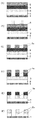
図2のように、上記の有機膜材料をそれぞれ、密集ホールパターン(ホール直径0.16μm、ホール深さ0.50μm、隣り合う二つのホールの中心間の距離0.32μm)を有するSiO2ウエハー基板上に塗布し、ホットプレートを用いて150℃で60秒間加熱し、有機膜8を形成した。使用した基板は図2(G)(俯瞰図)及び(H)(断面図)に示すような密集ホールパターンを有する下地基板7(SiO2ウエハー基板)である。得られた各ウエハー基板の断面形状を、走査型電子顕微鏡(SEM)を用いて観察し、ホール内部にボイド(空隙)なく、有機膜で充填されているかどうかを確認した。結果を表8に示す。埋め込み特性に劣る有機膜材料を用いた場合は、本評価において、ホール内部にボイドが発生する。埋め込み特性が良好な有機膜材料を用いた場合は、本評価において、図2(I)に示されるようにホール内部にボイドなく有機膜が充填される。
上記の有機膜材料をそれぞれ、巨大孤立トレンチパターン(図3(J)、トレンチ幅10μm、トレンチ深さ0.50μm)を有する下地基板9(SiO2ウエハー基板)上に塗布し、表9に記載の条件で焼成した後、トレンチ部分と非トレンチ部分の有機膜10の膜厚の差(図3(K)中のdelta 10)を、走査型電子顕微鏡(SEM)を用いて観察した。結果を表9に示す。本評価において、膜厚の差が小さいほど、平坦化特性が良好であるといえる。なお、本評価では、深さ0.50μmのトレンチパターンを、通常膜厚約0.3μmの有機膜材料を用いて平坦化しており、平坦化特性の優劣を評価するために、特殊な厳しい評価条件となっている。
有機膜材料(UDL−1〜24)を、それぞれ、トレンチパターン(トレンチ幅10μm、トレンチ深さ0.10μm)を有するSiO2ウエハー基板上に塗布し、表12に記載の条件で焼成することにより、有機膜(レジスト下層膜)を形成した。その上にレジスト中間層膜材料SOG1を塗布して200℃で60秒間ベークして膜厚35nmのレジスト中間層膜を形成し、その上にレジスト上層膜材料のArF用単層レジストを塗布し、105℃で60秒間ベークして膜厚100nmのフォトレジスト膜を形成した。フォトレジスト膜上に液浸保護膜材料(TC−1)を塗布し90℃で60秒間ベークし膜厚50nmの保護膜を形成した。
チャンバー圧力 10.0Pa
RFパワー 1,500W
CF4ガス流量 75sccm
O2ガス流量 15sccm
時間 15sec
チャンバー圧力 2.0Pa
RFパワー 500W
Arガス流量 75sccm
O2ガス流量 45sccm
時間 120sec
チャンバー圧力 2.0Pa
RFパワー 2,200W
C5F12ガス流量 20sccm
C2F6ガス流量 10sccm
Arガス流量 300sccm
O2 60sccm
時間 90sec
3…レジスト下層膜、 3a…レジスト下層膜パターン、 4…レジスト中間層膜、
4a…レジスト中間層膜パターン、 5…レジスト上層膜、
5a…レジストパターン、 6…所用部分、
7…密集ホールパターンを有する下地基板、 8…有機膜、
9…巨大孤立トレンチパターンを有する下地基板、 10…有機膜、
delta 10…トレンチ部分と非トレンチ部分の有機膜の膜厚の差。
(C−2)イソステアリン酸
(C−3)4−ヒドロキシ安息香酸
(C−4)9−アントラセンカルボン酸
(C−5)3−ヒドロキシ−2−ナフトエ酸
(C−6)6−ヒドロキシ−2−ナフトエ酸
(C−7)6−メトキシ−2−ナフトエ酸
(C−8)6−プロパルギルオキシ−2−ナフトエ酸
Claims (16)
- 下記一般式(1)で示される化合物を含むものであることを特徴とする有機膜材料。
- 前記一般式(1)で示される化合物が、下記一般式(4)で示される化合物であることを特徴とする請求項1に記載の有機膜材料。
- 前記Wが単結合又は下記式(5)で示される構造のいずれかであることを特徴とする請求項1又は請求項2に記載の有機膜材料。
- 前記一般式(1)で示される化合物が分子内に2個以上のQ1を有し、かつ、前記Q1として下記一般式(6)で示される構造及び下記一般式(7)で示される構造をそれぞれ1種以上含むものであることを特徴とする請求項1から請求項3のいずれか一項に記載の有機膜材料。
- 前記有機膜材料が、さらに、(A)酸発生剤、(B)架橋剤、(C)界面活性剤、(D)有機溶媒のうち1種以上を含有するものであることを特徴とする請求項1から請求項4のいずれか一項に記載の有機膜材料。
- 前記有機膜材料が、レジスト下層膜材料又は半導体装置製造用平坦化材料として用いられるものであることを特徴とする請求項1から請求項5のいずれか一項に記載の有機膜材料。
- リソグラフィーで用いられる多層レジスト膜のレジスト下層膜又は半導体製造用平坦化膜として機能する有機膜の形成方法であって、被加工基板上に請求項1から請求項6のいずれか一項に記載の有機膜材料をコーティングし、該有機膜材料を100℃以上600℃以下の温度で、10秒〜600秒間の範囲で熱処理することによって硬化膜を形成することを特徴とする有機膜形成方法。
- リソグラフィーで用いられる多層レジスト膜のレジスト下層膜又は半導体製造用平坦化膜として機能する有機膜の形成方法であって、被加工基板上に請求項1から請求項6のいずれか一項に記載の有機膜材料をコーティングし、該有機膜材料を、酸素濃度0.1%以上21%以下の雰囲気中で焼成することによって硬化膜を形成することを特徴とする有機膜形成方法。
- 前記被加工基板として、高さ30nm以上の構造体又は段差を有する被加工基板を用いることを特徴とする請求項7又は請求項8に記載の有機膜形成方法。
- 被加工基板にパターンを形成する方法であって、少なくとも、被加工基板上に請求項1から請求項6のいずれか一項に記載の有機膜材料を用いてレジスト下層膜を形成し、該レジスト下層膜上にケイ素原子を含有するレジスト中間層膜材料を用いてレジスト中間層膜を形成し、該レジスト中間層膜上にフォトレジスト組成物からなるレジスト上層膜材料を用いてレジスト上層膜を形成して多層レジスト膜とし、前記レジスト上層膜のパターン回路領域を露光した後、現像液で現像して前記レジスト上層膜にレジストパターンを形成し、該得られたレジストパターンをエッチングマスクにして前記レジスト中間層膜をエッチングしてレジスト中間層膜パターンを形成し、該得られたレジスト中間層膜パターンをエッチングマスクにして前記レジスト下層膜をエッチングしてレジスト下層膜パターンを形成し、さらに、該得られたレジスト下層膜パターンをエッチングマスクにして前記被加工基板をエッチングして前記被加工基板にパターンを形成することを特徴とするパターン形成方法。
- 前記レジスト中間層膜をエッチングマスクにして行う前記レジスト下層膜のエッチングを、酸素ガス又は水素ガスを主体とするエッチングガスを用いて行うことを特徴とする請求項10に記載のパターン形成方法。
- 被加工基板にパターンを形成する方法であって、少なくとも、被加工基板上に請求項1から請求項6のいずれか一項に記載の有機膜材料を用いてレジスト下層膜を形成し、該レジスト下層膜上にケイ素酸化膜、ケイ素窒化膜、及びケイ素酸化窒化膜から選ばれる無機ハードマスク中間膜を形成し、該無機ハードマスク中間膜上にフォトレジスト組成物からなるレジスト上層膜材料を用いてレジスト上層膜を形成して多層レジスト膜とし、前記レジスト上層膜のパターン回路領域を露光した後、現像液で現像して前記レジスト上層膜にレジストパターンを形成し、該得られたレジストパターンをエッチングマスクにして前記無機ハードマスク中間膜をエッチングして無機ハードマスク中間膜パターンを形成し、該得られた無機ハードマスク中間膜パターンをエッチングマスクにして前記レジスト下層膜をエッチングしてレジスト下層膜パターンを形成し、さらに、該得られたレジスト下層膜パターンをエッチングマスクにして前記被加工基板をエッチングして前記被加工基板にパターンを形成することを特徴とするパターン形成方法。
- 被加工基板にパターンを形成する方法であって、少なくとも、被加工基板上に請求項1から請求項6のいずれか一項に記載の有機膜材料を用いてレジスト下層膜を形成し、該レジスト下層膜上にケイ素酸化膜、ケイ素窒化膜、及びケイ素酸化窒化膜から選ばれる無機ハードマスク中間膜を形成し、該無機ハードマスク中間膜上に有機反射防止膜を形成し、該有機反射防止膜上にフォトレジスト組成物からなるレジスト上層膜材料を用いてレジスト上層膜を形成して多層レジスト膜とし、前記レジスト上層膜のパターン回路領域を露光した後、現像液で現像して前記レジスト上層膜にレジストパターンを形成し、該得られたレジストパターンをエッチングマスクにして前記有機反射防止膜と前記無機ハードマスク中間膜をエッチングして無機ハードマスク中間膜パターンを形成し、該得られた無機ハードマスク中間膜パターンをエッチングマスクにして前記レジスト下層膜をエッチングしてレジスト下層膜パターンを形成し、さらに、該得られたレジスト下層膜パターンをエッチングマスクにして前記被加工基板をエッチングして前記被加工基板にパターンを形成することを特徴とするパターン形成方法。
- 前記無機ハードマスク中間膜を、CVD法又はALD法によって形成することを特徴とする請求項12又は請求項13に記載のパターン形成方法。
- 前記被加工基板として高さ30nm以上の構造体又は段差を有する被加工基板を用いることを特徴とする請求項10から請求項14のいずれか一項に記載のパターン形成方法。
- 下記一般式(1)で示されるものであることを特徴とする化合物。
Priority Applications (4)
| Application Number | Priority Date | Filing Date | Title |
|---|---|---|---|
| JP2015098795A JP6372887B2 (ja) | 2015-05-14 | 2015-05-14 | 有機膜材料、有機膜形成方法、パターン形成方法、及び化合物 |
| US15/091,336 US9728420B2 (en) | 2015-05-14 | 2016-04-05 | Organic film composition, process for forming organic film, patterning process, and compound |
| TW105114490A TWI588613B (zh) | 2015-05-14 | 2016-05-11 | 有機膜材料、有機膜形成方法、圖案形成方法及化合物 |
| KR1020160058067A KR101911593B1 (ko) | 2015-05-14 | 2016-05-12 | 유기막 재료, 유기막 형성 방법, 패턴 형성 방법, 및 화합물 |
Applications Claiming Priority (1)
| Application Number | Priority Date | Filing Date | Title |
|---|---|---|---|
| JP2015098795A JP6372887B2 (ja) | 2015-05-14 | 2015-05-14 | 有機膜材料、有機膜形成方法、パターン形成方法、及び化合物 |
Publications (2)
| Publication Number | Publication Date |
|---|---|
| JP2016216367A true JP2016216367A (ja) | 2016-12-22 |
| JP6372887B2 JP6372887B2 (ja) | 2018-08-15 |
Family
ID=57277822
Family Applications (1)
| Application Number | Title | Priority Date | Filing Date |
|---|---|---|---|
| JP2015098795A Active JP6372887B2 (ja) | 2015-05-14 | 2015-05-14 | 有機膜材料、有機膜形成方法、パターン形成方法、及び化合物 |
Country Status (4)
| Country | Link |
|---|---|
| US (1) | US9728420B2 (ja) |
| JP (1) | JP6372887B2 (ja) |
| KR (1) | KR101911593B1 (ja) |
| TW (1) | TWI588613B (ja) |
Cited By (8)
| Publication number | Priority date | Publication date | Assignee | Title |
|---|---|---|---|---|
| WO2018135498A1 (ja) * | 2017-01-18 | 2018-07-26 | 三菱瓦斯化学株式会社 | 化合物、樹脂、組成物及びパターン形成方法 |
| WO2019054420A1 (ja) * | 2017-09-13 | 2019-03-21 | 日産化学株式会社 | 硬化性官能基を有する化合物を含む段差基板被覆組成物 |
| KR102029127B1 (ko) * | 2019-02-08 | 2019-10-07 | 영창케미칼 주식회사 | 반도체 제조 공정에 있어서 실리콘 또는 실리콘 화합물 패턴을 형성하기 위한 신규 방법 |
| EP3623867A1 (en) | 2018-09-13 | 2020-03-18 | Shin-Etsu Chemical Co., Ltd. | Patterning process |
| WO2020209327A1 (ja) * | 2019-04-11 | 2020-10-15 | 日産化学株式会社 | ヒドロキシアリール基末端の重合体を含む薬液耐性保護膜形成組成物 |
| JP2021105654A (ja) * | 2019-12-26 | 2021-07-26 | 信越化学工業株式会社 | 有機膜形成材料、有機膜の形成方法、パターン形成方法および化合物 |
| KR20230158039A (ko) | 2021-03-16 | 2023-11-17 | 닛산 가가쿠 가부시키가이샤 | 나프탈렌유닛함유 레지스트 하층막 형성 조성물 |
| JP7445583B2 (ja) | 2020-11-25 | 2024-03-07 | 信越化学工業株式会社 | レジスト下層膜材料、パターン形成方法、及びレジスト下層膜形成方法 |
Families Citing this family (8)
| Publication number | Priority date | Publication date | Assignee | Title |
|---|---|---|---|---|
| JP6714492B2 (ja) | 2015-12-24 | 2020-06-24 | 信越化学工業株式会社 | 有機膜形成用化合物、有機膜形成用組成物、有機膜形成方法、及びパターン形成方法 |
| JP6714493B2 (ja) | 2015-12-24 | 2020-06-24 | 信越化学工業株式会社 | 有機膜形成用化合物、有機膜形成用組成物、有機膜形成方法、及びパターン形成方法 |
| JP6853716B2 (ja) * | 2017-03-31 | 2021-03-31 | 信越化学工業株式会社 | レジスト下層膜材料、パターン形成方法、及びレジスト下層膜形成方法 |
| CN107201504B (zh) * | 2017-05-19 | 2019-04-05 | 京东方科技集团股份有限公司 | 真空干燥膜层的方法和显示器件 |
| JP6800105B2 (ja) * | 2017-07-21 | 2020-12-16 | 信越化学工業株式会社 | 有機膜形成用組成物、パターン形成方法、及び有機膜形成用樹脂 |
| JP6940335B2 (ja) | 2017-08-30 | 2021-09-29 | 信越化学工業株式会社 | 有機膜形成用組成物、半導体装置製造用基板、有機膜の形成方法、パターン形成方法、及び重合体 |
| JP7352530B2 (ja) * | 2020-10-05 | 2023-09-28 | 信越化学工業株式会社 | 有機膜形成用材料、半導体装置製造用基板、有機膜の形成方法、パターン形成方法、及び有機膜形成用化合物 |
| JP2023166976A (ja) * | 2022-05-10 | 2023-11-22 | 信越化学工業株式会社 | 金属酸化膜形成用組成物、パターン形成方法、及び金属酸化膜形成方法 |
Citations (21)
| Publication number | Priority date | Publication date | Assignee | Title |
|---|---|---|---|---|
| JPS5228793B1 (ja) * | 1970-06-09 | 1977-07-28 | ||
| PL95565B1 (pl) * | 1974-08-01 | 1977-10-31 | Sposob wytwarzania nienasyconych zywic bis-hy wych | |
| JPS63500183A (ja) * | 1985-05-17 | 1988-01-21 | エンスチチユ ナシヨナル ド リシエルシユ シミク アプリケ | 良好な熱的性質を有する重合体を製造する重合性組成物、それらを得る方法およびそれらの用途 |
| JPH024815A (ja) * | 1988-02-02 | 1990-01-09 | Minnesota Mining & Mfg Co <3M> | 熱可塑性、セルロースポリウレタンポリマー |
| US4925649A (en) * | 1987-06-12 | 1990-05-15 | The University Of Michigan | Radioiodinated diacylglycerol analogues and methods of use |
| JPH09179297A (ja) * | 1995-12-22 | 1997-07-11 | Mitsubishi Chem Corp | 光重合性組成物 |
| US5827836A (en) * | 1996-11-15 | 1998-10-27 | Clarion Pharmaceuticals Inc. | Retinoid glycerol phospholipid conjugates |
| JP2003533569A (ja) * | 2000-05-18 | 2003-11-11 | ダウ グローバル テクノロジーズ インコーポレイティド | ヒドロキシエステル誘導体中間体を製造する方法およびそれから製造されたエポキシ樹脂 |
| JP2004169198A (ja) * | 2002-11-18 | 2004-06-17 | Toray Ind Inc | 炭素繊維用前駆体繊維束およびその製造方法 |
| JP2005281955A (ja) * | 2004-03-04 | 2005-10-13 | Toray Ind Inc | 炭素繊維束 |
| JP2008209533A (ja) * | 2007-02-26 | 2008-09-11 | Jsr Corp | 着色層形成用感放射線性組成物、カラーフィルタおよびカラー液晶表示素子 |
| JP2009001792A (ja) * | 2007-06-25 | 2009-01-08 | Korea Kumho Petrochem Co Ltd | 有機反射防止膜用共重合体および組成物 |
| JP2009501788A (ja) * | 2005-07-20 | 2009-01-22 | エンジーケム カンパニー リミテッド | グリセロール誘導体の製造方法及びその中間体 |
| JP2009064000A (ja) * | 2007-08-16 | 2009-03-26 | Chisso Corp | 液晶配向剤、液晶配向膜および液晶表示素子 |
| JP2011140637A (ja) * | 2009-12-07 | 2011-07-21 | Dic Corp | セルロースエステル樹脂組成物、それを用いた光学フィルム及び液晶表示装置用偏光板 |
| WO2012077720A1 (ja) * | 2010-12-09 | 2012-06-14 | 協立化学産業株式会社 | 光重合開始剤に適した化合物、光重合開始剤及び光硬化性樹脂組成物 |
| JP2012206968A (ja) * | 2011-03-29 | 2012-10-25 | Osaka Gas Chem Kk | フルオレン骨格を有する(メタ)アクリレート |
| JP2014080567A (ja) * | 2012-09-25 | 2014-05-08 | Sekisui Chem Co Ltd | 硬化性樹脂組成物、封止材、上下導通材料、光電変換素子、色素増感太陽電池及び色素増感太陽電池モジュール |
| JP2014162911A (ja) * | 2013-02-27 | 2014-09-08 | Sekisui Chem Co Ltd | 硬化性樹脂組成物、封止材、上下導通材料、光電変換素子、色素増感太陽電池及び色素増感太陽電池モジュール |
| JP2015040224A (ja) * | 2013-08-20 | 2015-03-02 | 大阪ガスケミカル株式会社 | フルオレン骨格を有する多官能性(メタ)アクリレート |
| US20150064799A1 (en) * | 2013-08-30 | 2015-03-05 | National Kaohsiung Normal University | Excitation-dependent fluorescent organic nanoparticles |
Family Cites Families (24)
| Publication number | Priority date | Publication date | Assignee | Title |
|---|---|---|---|---|
| US3774305A (en) * | 1970-12-28 | 1973-11-27 | D Stoffey | Thermosetting acrylic resins and their use as binders in dental filling compositions |
| JP3009049B2 (ja) * | 1989-03-24 | 2000-02-14 | キヤノン株式会社 | インクジェット記録ヘッド、インクジェット記録ヘッドの表面処理方法、及びインクジェット記録装置 |
| TW269017B (ja) * | 1992-12-21 | 1996-01-21 | Ciba Geigy Ag | |
| JP3774668B2 (ja) | 2001-02-07 | 2006-05-17 | 東京エレクトロン株式会社 | シリコン窒化膜形成装置の洗浄前処理方法 |
| US6844273B2 (en) | 2001-02-07 | 2005-01-18 | Tokyo Electron Limited | Precleaning method of precleaning a silicon nitride film forming system |
| JP3981825B2 (ja) | 2002-12-24 | 2007-09-26 | 信越化学工業株式会社 | パターン形成方法及び下層膜形成材料 |
| KR100771800B1 (ko) | 2003-01-24 | 2007-10-30 | 도쿄 엘렉트론 가부시키가이샤 | 피처리 기판 상에 실리콘 질화막을 형성하는 cvd 방법 |
| TWI358612B (en) * | 2003-08-28 | 2012-02-21 | Nissan Chemical Ind Ltd | Polyamic acid-containing composition for forming a |
| JP4355943B2 (ja) | 2003-10-03 | 2009-11-04 | 信越化学工業株式会社 | フォトレジスト下層膜形成材料及びパターン形成方法 |
| US7303855B2 (en) | 2003-10-03 | 2007-12-04 | Shin-Etsu Chemical Co., Ltd. | Photoresist undercoat-forming material and patterning process |
| JP4388429B2 (ja) | 2004-02-04 | 2009-12-24 | 信越化学工業株式会社 | レジスト下層膜材料ならびにパターン形成方法 |
| JP4496432B2 (ja) | 2005-02-18 | 2010-07-07 | 信越化学工業株式会社 | フォトレジスト下層膜形成材料及びパターン形成方法 |
| KR100938065B1 (ko) | 2005-03-11 | 2010-01-21 | 신에쓰 가가꾸 고교 가부시끼가이샤 | 포토레지스트 하층막 형성 재료 및 패턴 형성 방법 |
| JP4662052B2 (ja) | 2005-03-11 | 2011-03-30 | 信越化学工業株式会社 | フォトレジスト下層膜形成材料及びパターン形成方法 |
| JP4575214B2 (ja) | 2005-04-04 | 2010-11-04 | 信越化学工業株式会社 | レジスト下層膜材料およびパターン形成方法 |
| JP4720988B2 (ja) * | 2005-07-11 | 2011-07-13 | 日産化学工業株式会社 | フルオレン構造を有する化合物を含むリソグラフィー用下層膜形成組成物 |
| JP4659678B2 (ja) | 2005-12-27 | 2011-03-30 | 信越化学工業株式会社 | フォトレジスト下層膜形成材料及びパターン形成方法 |
| JP4784784B2 (ja) | 2006-08-28 | 2011-10-05 | 日産化学工業株式会社 | 液状添加剤を含むレジスト下層膜形成組成物 |
| JP2008158002A (ja) | 2006-12-20 | 2008-07-10 | Jsr Corp | レジスト下層膜用組成物及びその製造方法 |
| JP4569786B2 (ja) | 2008-05-01 | 2010-10-27 | 信越化学工業株式会社 | 新規光酸発生剤並びにこれを用いたレジスト材料及びパターン形成方法 |
| JP5336306B2 (ja) | 2008-10-20 | 2013-11-06 | 信越化学工業株式会社 | レジスト下層膜形成方法、これを用いたパターン形成方法、及びレジスト下層膜材料 |
| CN103906624B (zh) * | 2011-09-26 | 2016-02-10 | 富士胶片株式会社 | 屏障积层体与其制造方法与其用途、屏障装置的制造方法、可聚合化合物与可聚合组合物 |
| JP5925721B2 (ja) * | 2012-05-08 | 2016-05-25 | 信越化学工業株式会社 | 有機膜材料、これを用いた有機膜形成方法及びパターン形成方法 |
| JP5835194B2 (ja) * | 2012-11-26 | 2015-12-24 | 信越化学工業株式会社 | レジスト下層膜材料及びパターン形成方法 |
-
2015
- 2015-05-14 JP JP2015098795A patent/JP6372887B2/ja active Active
-
2016
- 2016-04-05 US US15/091,336 patent/US9728420B2/en active Active
- 2016-05-11 TW TW105114490A patent/TWI588613B/zh active
- 2016-05-12 KR KR1020160058067A patent/KR101911593B1/ko active IP Right Grant
Patent Citations (21)
| Publication number | Priority date | Publication date | Assignee | Title |
|---|---|---|---|---|
| JPS5228793B1 (ja) * | 1970-06-09 | 1977-07-28 | ||
| PL95565B1 (pl) * | 1974-08-01 | 1977-10-31 | Sposob wytwarzania nienasyconych zywic bis-hy wych | |
| JPS63500183A (ja) * | 1985-05-17 | 1988-01-21 | エンスチチユ ナシヨナル ド リシエルシユ シミク アプリケ | 良好な熱的性質を有する重合体を製造する重合性組成物、それらを得る方法およびそれらの用途 |
| US4925649A (en) * | 1987-06-12 | 1990-05-15 | The University Of Michigan | Radioiodinated diacylglycerol analogues and methods of use |
| JPH024815A (ja) * | 1988-02-02 | 1990-01-09 | Minnesota Mining & Mfg Co <3M> | 熱可塑性、セルロースポリウレタンポリマー |
| JPH09179297A (ja) * | 1995-12-22 | 1997-07-11 | Mitsubishi Chem Corp | 光重合性組成物 |
| US5827836A (en) * | 1996-11-15 | 1998-10-27 | Clarion Pharmaceuticals Inc. | Retinoid glycerol phospholipid conjugates |
| JP2003533569A (ja) * | 2000-05-18 | 2003-11-11 | ダウ グローバル テクノロジーズ インコーポレイティド | ヒドロキシエステル誘導体中間体を製造する方法およびそれから製造されたエポキシ樹脂 |
| JP2004169198A (ja) * | 2002-11-18 | 2004-06-17 | Toray Ind Inc | 炭素繊維用前駆体繊維束およびその製造方法 |
| JP2005281955A (ja) * | 2004-03-04 | 2005-10-13 | Toray Ind Inc | 炭素繊維束 |
| JP2009501788A (ja) * | 2005-07-20 | 2009-01-22 | エンジーケム カンパニー リミテッド | グリセロール誘導体の製造方法及びその中間体 |
| JP2008209533A (ja) * | 2007-02-26 | 2008-09-11 | Jsr Corp | 着色層形成用感放射線性組成物、カラーフィルタおよびカラー液晶表示素子 |
| JP2009001792A (ja) * | 2007-06-25 | 2009-01-08 | Korea Kumho Petrochem Co Ltd | 有機反射防止膜用共重合体および組成物 |
| JP2009064000A (ja) * | 2007-08-16 | 2009-03-26 | Chisso Corp | 液晶配向剤、液晶配向膜および液晶表示素子 |
| JP2011140637A (ja) * | 2009-12-07 | 2011-07-21 | Dic Corp | セルロースエステル樹脂組成物、それを用いた光学フィルム及び液晶表示装置用偏光板 |
| WO2012077720A1 (ja) * | 2010-12-09 | 2012-06-14 | 協立化学産業株式会社 | 光重合開始剤に適した化合物、光重合開始剤及び光硬化性樹脂組成物 |
| JP2012206968A (ja) * | 2011-03-29 | 2012-10-25 | Osaka Gas Chem Kk | フルオレン骨格を有する(メタ)アクリレート |
| JP2014080567A (ja) * | 2012-09-25 | 2014-05-08 | Sekisui Chem Co Ltd | 硬化性樹脂組成物、封止材、上下導通材料、光電変換素子、色素増感太陽電池及び色素増感太陽電池モジュール |
| JP2014162911A (ja) * | 2013-02-27 | 2014-09-08 | Sekisui Chem Co Ltd | 硬化性樹脂組成物、封止材、上下導通材料、光電変換素子、色素増感太陽電池及び色素増感太陽電池モジュール |
| JP2015040224A (ja) * | 2013-08-20 | 2015-03-02 | 大阪ガスケミカル株式会社 | フルオレン骨格を有する多官能性(メタ)アクリレート |
| US20150064799A1 (en) * | 2013-08-30 | 2015-03-05 | National Kaohsiung Normal University | Excitation-dependent fluorescent organic nanoparticles |
Non-Patent Citations (1)
| Title |
|---|
| 田中賢治 等, ネットワークポリマー, vol. 28, no. 3, JPN6018005907, 2007, pages 87 - 92, ISSN: 0003743506 * |
Cited By (15)
| Publication number | Priority date | Publication date | Assignee | Title |
|---|---|---|---|---|
| JP7083455B2 (ja) | 2017-01-18 | 2022-06-13 | 三菱瓦斯化学株式会社 | 化合物、樹脂、組成物及びパターン形成方法 |
| JPWO2018135498A1 (ja) * | 2017-01-18 | 2019-11-07 | 三菱瓦斯化学株式会社 | 化合物、樹脂、組成物及びパターン形成方法 |
| WO2018135498A1 (ja) * | 2017-01-18 | 2018-07-26 | 三菱瓦斯化学株式会社 | 化合物、樹脂、組成物及びパターン形成方法 |
| WO2019054420A1 (ja) * | 2017-09-13 | 2019-03-21 | 日産化学株式会社 | 硬化性官能基を有する化合物を含む段差基板被覆組成物 |
| US11674051B2 (en) | 2017-09-13 | 2023-06-13 | Nissan Chemical Corporation | Stepped substrate coating composition containing compound having curable functional group |
| EP3623867A1 (en) | 2018-09-13 | 2020-03-18 | Shin-Etsu Chemical Co., Ltd. | Patterning process |
| US11488834B2 (en) | 2019-02-08 | 2022-11-01 | Young Chang Chemical Co., Ltd | Method for forming silicon or silicon compound pattern in semiconductor manufacturing process |
| WO2020162667A1 (ko) * | 2019-02-08 | 2020-08-13 | 영창케미칼 주식회사 | 반도체 제조 공정에 있어서 실리콘 또는 실리콘 화합물 패턴을 형성하기 위한 신규 방법 |
| KR102029127B1 (ko) * | 2019-02-08 | 2019-10-07 | 영창케미칼 주식회사 | 반도체 제조 공정에 있어서 실리콘 또는 실리콘 화합물 패턴을 형성하기 위한 신규 방법 |
| WO2020209327A1 (ja) * | 2019-04-11 | 2020-10-15 | 日産化学株式会社 | ヒドロキシアリール基末端の重合体を含む薬液耐性保護膜形成組成物 |
| US11965059B2 (en) | 2019-04-11 | 2024-04-23 | Nissan Chemical Corporation | Chemical-resistant protective film forming composition containing hydroxyaryl-terminated polymer |
| JP2021105654A (ja) * | 2019-12-26 | 2021-07-26 | 信越化学工業株式会社 | 有機膜形成材料、有機膜の形成方法、パターン形成方法および化合物 |
| JP7285209B2 (ja) | 2019-12-26 | 2023-06-01 | 信越化学工業株式会社 | 下層膜形成材料、下層膜の形成方法、及びパターン形成方法 |
| JP7445583B2 (ja) | 2020-11-25 | 2024-03-07 | 信越化学工業株式会社 | レジスト下層膜材料、パターン形成方法、及びレジスト下層膜形成方法 |
| KR20230158039A (ko) | 2021-03-16 | 2023-11-17 | 닛산 가가쿠 가부시키가이샤 | 나프탈렌유닛함유 레지스트 하층막 형성 조성물 |
Also Published As
| Publication number | Publication date |
|---|---|
| TW201704879A (zh) | 2017-02-01 |
| KR20160134536A (ko) | 2016-11-23 |
| TWI588613B (zh) | 2017-06-21 |
| JP6372887B2 (ja) | 2018-08-15 |
| KR101911593B1 (ko) | 2018-10-24 |
| US9728420B2 (en) | 2017-08-08 |
| US20160336189A1 (en) | 2016-11-17 |
Similar Documents
| Publication | Publication Date | Title |
|---|---|---|
| JP6372887B2 (ja) | 有機膜材料、有機膜形成方法、パターン形成方法、及び化合物 | |
| KR102528118B1 (ko) | 유기막 형성용 화합물, 유기막 형성용 조성물, 유기막 형성 방법 및 패턴 형성 방법 | |
| KR102565142B1 (ko) | 유기막 형성용 화합물, 유기막 형성용 조성물, 유기막 형성 방법 및 패턴 형성 방법 | |
| JP5229278B2 (ja) | ナフタレン誘導体、レジスト下層膜材料、レジスト下層膜形成方法及びパターン形成方法 | |
| JP5598489B2 (ja) | ビフェニル誘導体、レジスト下層膜材料、レジスト下層膜形成方法及びパターン形成方法 | |
| JP5925721B2 (ja) | 有機膜材料、これを用いた有機膜形成方法及びパターン形成方法 | |
| JP5118073B2 (ja) | レジスト下層膜形成方法及びこれを用いたパターン形成方法 | |
| JP5653880B2 (ja) | レジスト下層膜形成材料及びパターン形成方法 | |
| JP5385006B2 (ja) | レジスト下層膜材料及びこれを用いたパターン形成方法 | |
| JP5085569B2 (ja) | レジスト下層膜形成方法およびこれを用いたパターン形成方法 | |
| KR102353268B1 (ko) | 유기막 형성용 조성물, 패턴 형성 방법, 및 중합체 | |
| KR102484046B1 (ko) | 유기막 형성 재료, 유기막의 형성 방법, 패턴 형성 방법 및 화합물 | |
| CN112987495A (zh) | 有机膜形成材料、有机膜的形成方法、图案形成方法、以及化合物 | |
| KR102274471B1 (ko) | 유기막 형성용 조성물, 패턴 형성 방법 및 중합체 | |
| KR102474405B1 (ko) | 유기막 형성용 조성물, 패턴 형성 방법 및 중합체 | |
| KR20220092803A (ko) | 유기막 형성 재료, 그리고 패턴 형성 방법 및 중합체 | |
| JP7472011B2 (ja) | 有機膜形成材料、パターン形成方法ならびに化合物及び重合体 | |
| JP7103993B2 (ja) | 有機膜形成用組成物、パターン形成方法及び重合体 | |
| CN113341646A (zh) | 有机膜形成材料、有机膜形成方法、图案形成方法、以及化合物 | |
| KR20230051084A (ko) | 유기막 형성 재료, 패턴 형성 방법 및 화합물 |
Legal Events
| Date | Code | Title | Description |
|---|---|---|---|
| A621 | Written request for application examination |
Free format text: JAPANESE INTERMEDIATE CODE: A621 Effective date: 20170525 |
|
| A977 | Report on retrieval |
Free format text: JAPANESE INTERMEDIATE CODE: A971007 Effective date: 20180131 |
|
| A131 | Notification of reasons for refusal |
Free format text: JAPANESE INTERMEDIATE CODE: A131 Effective date: 20180227 |
|
| A521 | Request for written amendment filed |
Free format text: JAPANESE INTERMEDIATE CODE: A523 Effective date: 20180416 |
|
| TRDD | Decision of grant or rejection written | ||
| A01 | Written decision to grant a patent or to grant a registration (utility model) |
Free format text: JAPANESE INTERMEDIATE CODE: A01 Effective date: 20180626 |
|
| A61 | First payment of annual fees (during grant procedure) |
Free format text: JAPANESE INTERMEDIATE CODE: A61 Effective date: 20180712 |
|
| R150 | Certificate of patent or registration of utility model |
Ref document number: 6372887 Country of ref document: JP Free format text: JAPANESE INTERMEDIATE CODE: R150 |