JP2016018335A - Touch panel device and display device with touch position detection function - Google Patents
Touch panel device and display device with touch position detection function Download PDFInfo
- Publication number
- JP2016018335A JP2016018335A JP2014139945A JP2014139945A JP2016018335A JP 2016018335 A JP2016018335 A JP 2016018335A JP 2014139945 A JP2014139945 A JP 2014139945A JP 2014139945 A JP2014139945 A JP 2014139945A JP 2016018335 A JP2016018335 A JP 2016018335A
- Authority
- JP
- Japan
- Prior art keywords
- protective cover
- touch panel
- panel sensor
- thickness
- detection pattern
- Prior art date
- Legal status (The legal status is an assumption and is not a legal conclusion. Google has not performed a legal analysis and makes no representation as to the accuracy of the status listed.)
- Granted
Links
Images


Landscapes
- Position Input By Displaying (AREA)
Abstract
Description
本発明は、タッチパネルセンサと、タッチパネルセンサの観察者側に配置された保護カバーと、を備えるタッチパネル装置に関する。また本発明は、タッチパネルセンサ、保護カバーおよび表示装置を組み合わせることによって得られるタッチ位置検出機能付き表示装置に関する。 The present invention relates to a touch panel device including a touch panel sensor and a protective cover disposed on an observer side of the touch panel sensor. The present invention also relates to a display device with a touch position detection function obtained by combining a touch panel sensor, a protective cover, and a display device.
今日、入力手段として、タッチパネル装置が広く用いられている。タッチパネル装置は、タッチパネルセンサ、タッチパネルセンサからの信号を処理する検出制御部などを含んでいる。タッチパネル装置は、多くの場合、液晶ディスプレイや有機ELディスプレイ等の表示装置が組み込まれた種々の装置等(例えば、券売機、ATM装置、携帯電話、ゲーム機)に対する入力手段として、表示装置とともに用いられている。このような装置においては、タッチパネルセンサが表示装置の表示面上に配置されており、これによって、表示装置に対する極めて直接的な入力が可能になっている。タッチパネルセンサのうち表示装置の表示領域に対面する領域は透明になっており、タッチパネルセンサのこの領域が、接触位置(接近位置)を検出し得るアクティブエリアを構成するようになる。 Today, touch panel devices are widely used as input means. The touch panel device includes a touch panel sensor, a detection control unit that processes a signal from the touch panel sensor, and the like. In many cases, the touch panel device is used together with the display device as an input means for various devices including a display device such as a liquid crystal display or an organic EL display (for example, a ticket vending machine, an ATM device, a mobile phone, a game machine). It has been. In such a device, the touch panel sensor is disposed on the display surface of the display device, thereby enabling extremely direct input to the display device. The area | region which faces the display area of a display apparatus among touch panel sensors is transparent, and this area | region of a touch panel sensor comprises the active area which can detect a contact position (approach position).
タッチパネルセンサとして、投影型容量結合方式のタッチパネルセンサが知られている。容量結合方式のタッチパネルセンサにおいては、位置を検知されるべき外部導体(典型的には、指)が誘電体を介してタッチパネルセンサに接触(接近)する際、新たに奇生容量が発生する。この奇生容量に起因する静電容量の変化に基づいて、タッチパネルセンサ上における外部導体の位置が検出される。このような投影型容量結合方式のタッチパネルセンサは、基材と、基材上に設けられた複数の検出パターンと、を備えている。検出パターンには、パルス信号などの電気信号が伝達されている。そして、外部導体の接近に起因して生じるパルス信号の変化を解析することにより、タッチパネルセンサ上における外部導体の位置を検出することができる。 As a touch panel sensor, a projection capacitive coupling type touch panel sensor is known. In the capacitive coupling type touch panel sensor, when an external conductor (typically, a finger) whose position is to be detected contacts (approaches) the touch panel sensor via a dielectric, a strange capacitance is newly generated. The position of the external conductor on the touch panel sensor is detected on the basis of the change in capacitance caused by this strange capacitance. Such a projected capacitive coupling touch panel sensor includes a base material and a plurality of detection patterns provided on the base material. An electrical signal such as a pulse signal is transmitted to the detection pattern. The position of the external conductor on the touch panel sensor can be detected by analyzing the change in the pulse signal caused by the approach of the external conductor.
タッチパネル装置は一般に、タッチパネルセンサに加えて、タッチパネルセンサの観察者側に配置された保護カバーを備えている(例えば特許文献1参照)。この場合、指などの外部導体は保護カバーに接触することになる。このため、保護カバーを設けることにより、タッチパネルセンサや表示装置を外部から保護することができる。このような保護カバーは、ガラスなどの透明な誘電体から構成される。 In general, the touch panel device includes a protective cover disposed on the observer side of the touch panel sensor in addition to the touch panel sensor (see, for example, Patent Document 1). In this case, an external conductor such as a finger comes into contact with the protective cover. For this reason, by providing a protective cover, the touch panel sensor and the display device can be protected from the outside. Such a protective cover is made of a transparent dielectric such as glass.
保護カバーとしては、その両面が平坦面からなるものが主に用いられている。その他にも、特許文献1においては、タッチパネルセンサの中心部におけるタッチ位置の検出感度と、タッチパネルセンサの端部近傍におけるタッチ位置の検出感度とを均一にするため、保護カバーに湾曲面を形成することが提案されている。
As the protective cover, a cover having both flat surfaces is mainly used. In addition, in
従来、タッチパネルセンサの観察者側に配置された保護カバーとしては、強化ガラスが一般に用いられている。強化ガラスとは、ガラスを加熱した後に急速に冷却するという熱処理を実施することにより、ガラスの表面に圧縮応力層が形成され、ガラスの内部に引張応力層が形成されたガラスのことである。このような強化ガラスにおいては、その一方の側の面(以下、第1面とも称する)に何らかの打撃力が加えられ、これによってその表面にクラックなどの傷が形成された場合であっても、圧縮応力層のため、傷が拡大することが防がれる。このため、強化ガラスは割れにくくなっている。 Conventionally, tempered glass is generally used as a protective cover disposed on the viewer side of the touch panel sensor. The tempered glass is a glass in which a compressive stress layer is formed on the surface of the glass and a tensile stress layer is formed inside the glass by performing a heat treatment in which the glass is heated and then rapidly cooled. In such tempered glass, even if some striking force is applied to the surface on one side thereof (hereinafter also referred to as the first surface), and a scratch such as a crack is formed on the surface thereof, Due to the compressive stress layer, the damage is prevented from expanding. For this reason, the tempered glass is difficult to break.
しかしながら、強化ガラスの上述のような構造のため、強化ガラスの表面を切削して所望の形状を得ることは困難である。なぜなら、強化ガラスの表面を切削することは、表面の圧縮応力層を除去することになり、この結果、強化ガラスが割れやすくなってしまうからである。従って、湾曲面などの特異な形状を有する面を備えた強化ガラスを作製するためには、強化のための熱処理を実施する前にガラスを成形して湾曲面や傾斜面などをガラスに付与しておくことになる。しかしながら、ガラスの成形には大規模な生産設備が必要になる。従って、湾曲面などの特異な形状を有する保護カバーを、小ロットで製造することは容易ではない。 However, due to the above-described structure of tempered glass, it is difficult to obtain a desired shape by cutting the surface of tempered glass. This is because cutting the surface of the tempered glass removes the compressive stress layer on the surface, and as a result, the tempered glass tends to break. Therefore, in order to produce a tempered glass having a surface having a unique shape such as a curved surface, the glass is molded before the heat treatment for tempering, and a curved surface or an inclined surface is imparted to the glass. I will keep it. However, large-scale production facilities are required for glass forming. Therefore, it is not easy to manufacture a protective cover having a unique shape such as a curved surface in a small lot.
本発明は、このような点を考慮してなされたものであり、タッチパネルセンサと、湾曲面などの特異な形状を有するとともに容易に入手可能な保護カバーと、を備えたタッチパネル装置に関する。また本発明は、タッチパネルセンサ、保護カバーおよび表示装置を組み合わせることによって得られるタッチ位置検出機能付き表示装置に関する。 The present invention has been made in consideration of such points, and relates to a touch panel device including a touch panel sensor and a protective cover that has a unique shape such as a curved surface and is easily available. The present invention also relates to a display device with a touch position detection function obtained by combining a touch panel sensor, a protective cover, and a display device.
本発明は、タッチパネルセンサと、タッチパネルセンサの観察者側に配置された保護カバーと、を備えるタッチパネル装置であって、前記タッチパネルセンサは、タッチ位置を検出され得る領域に対応するアクティブエリアと、アクティブエリアの周辺に位置する非アクティブエリアと、を含む基材と、前記アクティブエリアに配置された検出パターンと、前記非アクティブエリアに配置され、前記検出パターンに電気的に接続された額縁配線と、を備え、前記保護カバーは、観察者側の第1面と、前記タッチパネルセンサ側の平坦な第2面と、を含み、前記保護カバーは、プラスチック成形体から構成されており、前記保護カバーの前記第1面は、前記保護カバーの端部の厚みが前記保護カバーの中心部の厚みとは異なるよう、構成されており、前記タッチパネルセンサの前記検出パターンは、遮光性および導電性を有する複数の導線を網目状に配置することによって構成されている、タッチパネル装置である。 The present invention is a touch panel device including a touch panel sensor and a protective cover disposed on an observer side of the touch panel sensor, the touch panel sensor including an active area corresponding to a region where a touch position can be detected, and an active area A base material including an inactive area located around the area, a detection pattern arranged in the active area, a frame wiring arranged in the inactive area and electrically connected to the detection pattern, The protective cover includes a first surface on the observer side and a flat second surface on the touch panel sensor side, and the protective cover is made of a plastic molded body, The first surface is configured such that the thickness of the end portion of the protective cover is different from the thickness of the central portion of the protective cover. Ri, the detection pattern of the touch panel sensor, a plurality of wires having a light shielding property and conductivity are formed by placing a mesh shape, a touch panel device.
本発明によるタッチパネル装置において、前記保護カバーの前記第1面は、前記保護カバーの端部の厚みが前記保護カバーの中心部の厚みよりも小さくなるよう、構成されていてもよい。この場合、前記保護カバーの前記第1面は、観察者側に向かって凸となる湾曲面を含んでいてもよい。また、前記保護カバーの前記第1面は、前記保護カバーの中心部を含む平坦面と、前記平坦面の外縁から外側に向かうにつれて前記タッチパネルセンサ側へ傾斜した傾斜面と、を含んでいてもよい。 In the touch panel device according to the present invention, the first surface of the protective cover may be configured such that the thickness of the end portion of the protective cover is smaller than the thickness of the central portion of the protective cover. In this case, the first surface of the protective cover may include a curved surface that is convex toward the viewer side. The first surface of the protective cover may include a flat surface including a central portion of the protective cover, and an inclined surface inclined toward the touch panel sensor as it goes outward from an outer edge of the flat surface. Good.
本発明によるタッチパネル装置において、前記タッチパネルセンサの前記アクティブエリアと前記非アクティブエリアとの間の境界に対応する位置における前記保護カバーの厚みは、好ましくは、前記保護カバーの中心部の厚みの50〜80%の範囲内になっている。 In the touch panel device according to the present invention, the thickness of the protective cover at a position corresponding to the boundary between the active area and the inactive area of the touch panel sensor is preferably 50 to 50% of the thickness of the central portion of the protective cover. It is within the range of 80%.
本発明によるタッチパネル装置において、前記保護カバーの前記第1面は、前記保護カバーの端部の厚みが前記保護カバーの中心部の厚みよりも大きくなるよう、構成されていてもよい。この場合、前記保護カバーの前記第1面は、前記タッチパネルセンサ側に向かって凹んだ湾曲面を含んでいてもよい。 In the touch panel device according to the present invention, the first surface of the protective cover may be configured such that the thickness of the end portion of the protective cover is larger than the thickness of the central portion of the protective cover. In this case, the first surface of the protective cover may include a curved surface that is recessed toward the touch panel sensor side.
本発明によるタッチパネル装置において、前記保護カバーは、好ましくは、アクリル樹脂、ポリカーボネート樹脂、ポリエチレンテレフタレート樹脂またはそれらの積層体から構成されている。 In the touch panel device according to the present invention, the protective cover is preferably made of an acrylic resin, a polycarbonate resin, a polyethylene terephthalate resin, or a laminate thereof.
本発明は、表示装置と、前記表示装置の表示面上に配置されたタッチパネルセンサと、タッチパネルセンサの観察者側に配置された保護カバー と、を備え、前記タッチパネルセンサは、タッチ位置を検出され得る領域に対応するアクティブエリアと、アクティブエリアの周辺に位置する非アクティブエリアと、を含む基材と、前記アクティブエリアに配置された検出パターンと、前記非アクティブエリアに配置され、前記検出パターンに電気的に接続された額縁配線と、を備え、前記保護カバーは、観察者側の第1面と、前記タッチパネルセンサ側の平坦な第2面と、を含み、前記保護カバーは、プラスチック成形体から構成されており、前記保護カバーの前記第1面は、前記保護カバーの端部の厚みが前記保護カバーの中心部の厚みとは異なるよう、構成されており、前記タッチパネルセンサの前記検出パターンは、遮光性および導電性を有する複数の導線を網目状に配置することによって構成されている、タッチ位置検出機能付き表示装置である。 The present invention includes a display device, a touch panel sensor disposed on a display surface of the display device, and a protective cover disposed on an observer side of the touch panel sensor, and the touch panel sensor detects a touch position. A base material including an active area corresponding to a region to be obtained, a non-active area located around the active area, a detection pattern disposed in the active area, and a detection pattern disposed in the non-active area. A frame wiring electrically connected, and the protective cover includes a first surface on the viewer side and a flat second surface on the touch panel sensor side, and the protective cover is a plastic molded body. The first surface of the protective cover has a thickness of an end portion of the protective cover different from a thickness of a central portion of the protective cover. It is comprised so that it may become, The said detection pattern of the said touchscreen sensor is a display apparatus with a touch position detection function comprised by arrange | positioning the several conducting wire which has light-shielding property and electroconductivity in mesh shape.
本発明によれば、保護カバーがプラスチック成形体から構成されている。このため、湾曲面や傾斜面などの様々な形状を容易に保護カバーに持たせることができる。このことにより、タッチパネル装置およびタッチ位置検出機能付き表示装置のデザイン性を向上させることができる。また本発明によれば、タッチパネルセンサの検出パターンは、遮光性および導電性を有する複数の導線を網目状に配置することによって構成されている。従って、ITOなどの透明導電材料によって検出パターンが構成されるタイプのタッチパネルセンサに比べて、検出パターンの電気抵抗値を小さくすることができる。このため、ノイズに対するタッチパネルセンサの耐性を高くすることができ、これによって、検出感度を改善することができる。従って、保護カバーをプラスチック成形体で構成することによって、ガラスタイプの保護カバーに比べて静電容量が低下する場合であっても、所望の検出感度を維持することができる。 According to the present invention, the protective cover is made of a plastic molded body. For this reason, various shapes, such as a curved surface and an inclined surface, can be easily given to a protective cover. As a result, the design of the touch panel device and the display device with a touch position detection function can be improved. According to the invention, the detection pattern of the touch panel sensor is configured by arranging a plurality of conductive wires having light shielding properties and conductivity in a mesh shape. Therefore, the electrical resistance value of the detection pattern can be reduced as compared with a touch panel sensor of a type in which the detection pattern is configured by a transparent conductive material such as ITO. For this reason, the tolerance of the touch panel sensor with respect to noise can be increased, and thereby the detection sensitivity can be improved. Therefore, by configuring the protective cover with a plastic molded body, it is possible to maintain a desired detection sensitivity even when the capacitance is lower than that of the glass-type protective cover.
以下、図1乃至図5を参照して、本発明の実施の形態の一例について説明する。なお、本明細書に添付する図面においては、図示と理解のしやすさの便宜上、適宜縮尺および縦横の寸法比等を、実物のそれらから変更し誇張してある。 Hereinafter, an example of an embodiment of the present invention will be described with reference to FIGS. In the drawings attached to the present specification, for the sake of illustration and ease of understanding, the scale, the vertical / horizontal dimension ratio, and the like are appropriately changed and exaggerated from those of the actual ones.
タッチパネル装置およびタッチ位置検出機能付き表示装置
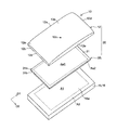
はじめに図1を参照して、タッチ位置検出機能付き表示装置10について説明する。図1に示すように、タッチ位置検出機能付き表示装置10は、液晶ディスプレイや有機ELディスプレイなどの表示装置15と、表示装置15の観察者側に配置されたタッチパネルセンサ30と、タッチパネルセンサ30の観察者側に配置された保護カバー12と、を組み合わせることによって構成されている。表示装置15は、表示面16aを有した表示パネル16と、表示パネル16に接続された表示制御部(図示せず)と、を有している。表示パネル16は、映像を表示することができるアクティブエリアA1と、アクティブエリアA1を取り囲むようにしてアクティブエリアA1の外側に配置された非アクティブエリア(額縁領域とも呼ばれる)A2と、を含んでいる。表示制御部は、表示されるべき映像に関する情報を処理し、映像情報に基づいて表示パネル16を駆動する。表示パネル16は、表示制御部の制御信号に基づいて、所定の映像を表示面16aに表示する。すなわち、表示装置15は、文字や図等の情報を映像として出力する出力装置としての役割を担っている。
Touch Panel Device and Display Device with Touch Position Detection Function First, a
図1に示すように、タッチパネルセンサ30は、表示装置15の表示面16aに、例えば接着層(図示せず)を介して接着されている。同様に、保護カバー12も、接着層(図示せず)などを介してタッチパネルセンサ30に接着されている。
As shown in FIG. 1, the
タッチパネルセンサ
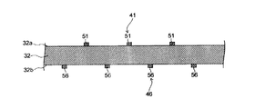
次に図2を参照して、タッチパネルセンサ30の概略について説明する。図2は、観察者側から見た場合のタッチパネルセンサ30を示す平面図である。
Touch Panel Sensor Next, an outline of the
ここでは、タッチパネルセンサ30が、投影型の静電容量結合方式のタッチパネルセンサとして構成される例について説明する。なお、「容量結合」方式は、タッチパネルの技術分野において「静電容量」方式や「静電容量結合」方式等とも呼ばれており、本件では、これらの「静電容量」方式や「静電容量結合」方式等と同義の用語として取り扱う。典型的な静電容量結合方式のタッチパネルセンサは、透光性を有する導電性のパターンを有しており、外部の導体(典型的には人間の指)がタッチパネルセンサに接近することにより、外部の導体とタッチパネルセンサの導電性のパターンとの間でコンデンサ(静電容量)が形成される。そして、このコンデンサの形成に伴った電気的な状態の変化に基づき、タッチパネルセンサ上において外部導体が接近している位置の位置座標が特定される。なお本実施の形態によるタッチパネルセンサ30は、自己容量方式のものであってもよく、相互容量方式のものであってもよい。
Here, an example in which the
図2に示すように、タッチパネルセンサ30は、観察者側を向く第1面32aおよび表示装置側を向く第2面32bを含み、透光性を有する基材32と、基材32の第1面32a上に設けられ、第1方向D1に延びる複数の第1検出パターン41と、基材32の第2面32b上に設けられ、第1方向D1に交差する、例えば第1方向D1に直交する第2方向D2に延びる複数の第2検出パターン46と、を備えている。図2に示すように、第1検出パターン41および第2検出パターン46はそれぞれ帯状に延びている。また、複数の第1検出パターン41は一定の配列ピッチで第2方向D2に並べられており、複数の第2検出パターン46も一定の配列ピッチで第1方向D1に並べられている。通常は、第2方向D2における第1検出パターン41の配列ピッチと、第1方向D1における第2検出パターン46の配列ピッチとは同一になっている。第1検出パターン41および第2検出パターン46の配列ピッチは、タッチ位置の検出に関して求められる分解能に応じて定められるが、例えば数mmになっている。なお図2においては、基材32の第1面32a側に設けられている構成要素が実線で表され、基材32の第2面32b側に設けられている構成要素が点線で表されている。
As shown in FIG. 2, the
図1に示すように、タッチパネルセンサ30の基材32は、タッチ位置を検出され得る領域に対応する矩形状のアクティブエリアAa1と、アクティブエリアAa1の周辺に位置する矩形枠状の非アクティブエリアAa2と、を含んでいる。アクティブエリアAa1および非アクティブエリアAa2はそれぞれ、表示パネル16のアクティブエリアA1および非アクティブエリアA2に対応して区画されたものである。
As shown in FIG. 1, the
基材32を構成する材料としては、例えば、ポリエチレンテレフタレート(PET)、シクロオレフィンポリマー(COP)やガラスなど、十分な透光性を有する材料が用いられる。基材32が例えばPETを含む場合、PETの厚みは例えば100〜200μmの範囲内になっている。なお図2に示す第1検出パターン41、第2検出パターン46、額縁配線44a,49aや端子部44b,49bを適切に保持することができる限りにおいて、基材32の具体的な構成が特に限られることはない。例えば、PET層などの表面に設けられたハードコート層がさらに基材32に含まれていてもよい。すなわち本実施の形態において、基材32とは、何らかの具体的な構造や材料を意味するものではなく、タッチパネルセンサ30を構成する第1検出パターン41や第2検出パターン46などのパターンの下地となるものを意味するに過ぎない。
As a material constituting the
上述の第1検出パターン41および第2検出パターン46は、アクティブエリアAa1内に配置されている。また非アクティブエリアAa2のうち基材32の第1面32a上には、各第1検出パターン41に電気的に接続された複数の第1額縁配線44aと、基材32の外縁近傍に配置され、各第1額縁配線44aに電気的に接続された複数の第1端子部44bと、が設けられている。さらに、非アクティブエリアAa2のうち基材32の第2面32b上には、各第2検出パターン46に電気的に接続された複数の第2額縁配線49aと、基材32の外縁近傍に配置され、各第2額縁配線49aに電気的に接続された複数の第2端子部49bと、が設けられている。
The
保護カバー
次に図1および図5を参照して、保護カバー12について説明する。図1および図5において、保護カバー12の観察者側の面(以下、第1面とも称する)が符号12aで示されており、保護カバー12のタッチパネルセンサ30側の面(以下、第2面とも称する)が符号12bで示されている。
Protective Cover Next, the
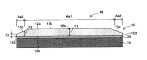
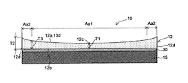
保護カバー12は、平面視において、タッチパネルセンサ30の第1検出パターン41と同様に第1方向D1に延びる一対の辺と、タッチパネルセンサ30の第2検出パターン46と同様に第2方向D2に延びる一対の辺と、を含む矩形状を有している。図1において、第1方向D1における保護カバー12の端部が符号12dで示されており、第2方向D2における保護カバー12の端部が符号12eで示されている。図5は、第1方向D1に平行な方向においてタッチ位置検出機能付き表示装置10を切断した場合を示す断面図である。
In plan view, the
図5に示すように、本実施の形態において、保護カバー12の第2面12bは、平坦面として構成されており、一方、第1面12aは、観察者側に向かって凸となる湾曲面13aとして構成されている。保護カバー12の第1面12aが湾曲面13aを含むことにより、タッチ位置検出機能付き表示装置10全体として、その前面に湾曲形状を持たせることができ、これによって、タッチ位置検出機能付き表示装置10のデザイン性を向上させることができる。なお、保護カバー12の第2面12bは平坦面で構成されているため、保護カバー12と組み合わされるタッチパネルセンサ30としては、広く流通している平坦なタッチパネルセンサ30を用いることが可能である。湾曲した前面を有するタッチ位置検出機能付き表示装置10が用いられる場所は特には限られないが、例えば、車のダッシュボードにタッチ位置検出機能付き表示装置10を組み込むことが考えられる。この場合、車のダッシュボードの湾曲形状に沿った湾曲面13aを含む保護カバー12を用いることにより、ダッシュボードとタッチ位置検出機能付き表示装置10とが一体的に見えるという効果を生じさせることができる。
As shown in FIG. 5, in the present embodiment, the
なお図5においては、第1方向D1に平行な方向において保護カバー12を切断した場合の断面図において、保護カバー12の第1面12aが湾曲面13aを含む例を示したが、これに限られることはない。図示はしないが、第2方向D2に平行な方向において保護カバー12を切断した場合の断面図において、保護カバー12の第1面12aが湾曲面を含んでいてもよい。
5 shows an example in which the
図5において、保護カバー12の中心部における保護カバー12の厚みが符号T1で示されており、保護カバー12の端部12dにおける保護カバー12の厚みが符号T2で示されている。ここでは、第1面12aが、観察者側に向かって凸となる湾曲面13aを含むため、保護カバー12の端部12dの厚みT2が、保護カバー12の中心部の厚みT1よりも小さくなっている。厚みT1に対する厚みT2の比率は、保護カバー12に求められるデザインなどに応じて適切に設定される。なお保護カバー12の中心部とは、平面視における保護カバー12の中心点12cに対応する部分のことである。保護カバー12の中心部の厚みT1は、タッチ位置検出機能付き表示装置10に求められる検出感度や、保護カバー12に対して求められる強度などに応じて適切に設定されるが、例えば約1mmになっている。
In FIG. 5, the thickness of the
図5において、タッチパネルセンサ30のアクティブエリアAa1と非アクティブエリアAa2との間の境界に対応する位置における保護カバー12の厚みが符号T3で示されている。好ましくは、厚みT3は、保護カバー12の中心部の厚みT1の50〜80%の範囲内になっている。厚みT3をこのように設定することにより、アクティブエリアAa1の中心部における、外部導体と検出パターン41,46との間の静電容量と、アクティブエリアAa1の外縁近傍における、外部導体と検出パターン41,46との間の静電容量との差が大きくなりすぎることを防ぐことができる。これによって、タッチ位置の検出感度が位置によってばらついてしまうことを抑制できる。
In FIG. 5, the thickness of the
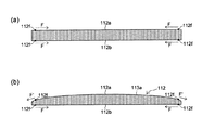
以下、図5に示すような湾曲面13aを含む保護カバー12を作製する方法について説明する。ここではまず、本実施の形態との比較のため、強化ガラスを湾曲形状に加工することによって、比較の形態による保護カバー112を作製する場合について、図6(a)(b)を参照して説明する。
Hereinafter, a method for producing the
(比較の形態)
はじめに図6(a)に示すように、平坦な第1面112aおよび第2面112bを有する強化ガラスを準備する。強化ガラスを得る方法としては、例えば、化学強化や物理強化(風冷強化)が知られている。例えば化学強化においては、歪点以下の温度で、ガラス中に含まれるアルカリイオンを、よりイオン半径の大きな他のアルカリイオンに交換するという化学的な処理が実施される。これによって、イオンが交換された表層付近に圧縮応力を発生させることができる。例えば、強化ガラスの第1面112a上および第2面112b上の各点112fには、内側に向かう圧縮応力Fが働くようになる。一方、図示はしないが、強化ガラスの内部には、表面の圧縮応力Fと釣り合う引張応力が働いている。
次に、強化ガラスの第1面112aを、切削などによって加工する。これによって図6(b)に示すように、第1面112aに湾曲面113aを形成する。しかしながら、この際、第1面112aの圧縮応力層が除去されるため、第1面112aには引張応力F’が働くようになってしまう。この場合、第1面112aにクラックなどの傷が形成されると、引張応力F’は、傷を拡大させる方向に働く。このように、圧縮応力層が除去された後の強化ガラスは、傷に対して非常に弱いものとなってしまう。
(Comparison form)
First, as shown in FIG. 6A, a tempered glass having a flat
Next, the
なお、湾曲面113aを含む保護カバー112を強化ガラスで作製する方法としては、はじめに、型などを用いて板ガラスを加工して板ガラスに湾曲面113aを付与し、その後、板ガラスに熱処理を施して板ガラスを強化する、という方法も考えらえる。しかしながら、型などを用いて板ガラスを加工することや、板ガラスに熱処理を施すことには、大規模な生産設備を要する。従ってこの方法は、容易に実施され得るものではない。
In addition, as a method of manufacturing the
このような課題を考慮し、本件発明者らは、湾曲面13aを備えた保護カバー12を、プラスチック成形体として構成することを提案する。プラスチック成形体とは、合成樹脂が成形され固化されることによって得られる部材のことである。プラスチックの成形方法は特には限られないが、例えば射出成形法やシート成形法などが採用され得る。合成樹脂は、ガラスに比べて低い温度で成形され得る。このため、保護カバー12をプラスチック成形体として構成することにより、湾曲面13aを容易に保護カバー12に持たせることができる。また、外側に向かって凸となる湾曲面の形状は、合成樹脂製の眼鏡レンズなどにおいても既に採用されている、高い強度を実現できる形状である。このため本実施の形態によれば、デザイン性に優れ、かつ十分な強度を有する保護カバー12を容易に提供することができる。
In consideration of such a problem, the present inventors propose to configure the
保護カバー12を構成する合成樹脂としては、十分な透光性および加工性を有する材料が用いられる。例えば、アクリル樹脂、ポリカーボネート樹脂、ポリエチレンテレフタレート樹脂またはそれらの積層体を用いることができる。
As the synthetic resin constituting the
ところで、合成樹脂の比誘電率は、ガラスの比誘電率に比べて一般に低い。例えば、ガラスの比誘電率が約1.7であるのに対して、アクリル樹脂、ポリカーボネート樹脂などの合成樹脂の比誘電率は約1.3になっている。このため、本実施の形態による保護カバー12が用いられる場合、ガラスによって構成された保護カバーが用いられる場合に比べて、両者の厚みが同等であれば、外部導体とタッチパネルセンサ30の検出パターン41,46との間の静電容量が小さくなる。静電容量の低下は、タッチパネルセンサ30の検出感度の低下を導き得る。
By the way, the relative dielectric constant of synthetic resin is generally lower than that of glass. For example, while the relative dielectric constant of glass is about 1.7, the relative dielectric constant of synthetic resins such as acrylic resin and polycarbonate resin is about 1.3. For this reason, when the
このような課題を考慮して、本件発明者らは、合成樹脂製の保護カバー12と、メッシュタイプのタッチパネルセンサ30の検出パターン41,46とを組み合わせることを提案する。メッシュタイプのタッチパネルセンサ30の検出パターン41,46においては、検出パターン41,46が金属材料から構成されるので、ITOなどの透明導電材料によって検出パターンが構成されるタイプのタッチパネルセンサに比べて、検出パターンの電気抵抗値を小さくすることができる。このため、ノイズに対するタッチパネルセンサ30の耐性を高くすることができ、このことにより、検出感度を改善することができる。すなわち、合成樹脂製の保護カバー12と、メッシュタイプのタッチパネルセンサ30の検出パターン41,46との組合せによれば、合成樹脂を採用したことによる、保護カバー12の静電容量の低下分を、検出パターン41,46の電気抵抗値の改善によって補償することができる。
In consideration of such problems, the present inventors propose to combine the
以下、メッシュタイプのタッチパネルセンサ30の検出パターン41,46の一例について、図3A乃至図4を参照して説明する。図3Aは、図2において符号IIIが付された一点鎖線で囲まれた部分における第1検出パターン41を、観察者側から見た場合を示す平面図であり、図3Bは、図2において符号IIIが付された一点鎖線で囲まれた部分における第2検出パターン46を、観察者側から見た場合、すなわち基材32を透かして第2検出パターン46を見た場合を示す平面図である。また図4は、第1検出パターン41および第2検出パターン46を含むタッチパネルセンサ30を示す断面図である。
Hereinafter, an example of the
(第1検出パターン)
はじめに第1検出パターン41について説明する。本実施の形態において、第1検出パターン41は、遮光性および導電性を有する第1導線51であって、各第1導線51の間に開口部51aが形成されるよう網目状に配置された第1導線51から構成されている。同様に、第2検出パターン46は、遮光性および導電性を有する第2導線56であって、各第2導線56の間に開口部56aが形成されるよう網目状に配置された第2導線56から構成されている。第1導線51および第2導線56は各々、図4に示すように、金属材料からなる金属層を含んでいる。なお第1導線51および第2導線56を構成する金属層には、その表面における光の反射を抑制するための黒化処理などが施されていてもよい。
(First detection pattern)
First, the
第1検出パターン41全体の面積のうち開口部51aによって占められる面積の比率(以下、開口率と称する)が十分に高くなり、これによって、表示装置15からの映像光が適切な透過率でタッチパネルセンサ30のアクティブエリアAa1を透過することができる限りにおいて、第1導線51の寸法や形状が特に限られることはない。例えば図3Aに示す例において、第1検出パターン41は、菱形に形成された第1導線51を第1方向D1に沿って並べることによって構成されている。この場合、菱形の内角のうち鋭角になる内角が第1方向D1に沿って並ぶよう、第1導線51が構成されている。開口率の範囲は、表示装置15から放出される映像光の特性などに応じて適宜設定される。図3Aにおいて、第1検出パターン41の幅が符号W1で表されており、隣接する2つの第1検出パターン41の間の間隔が符号S1で表されている。
The ratio of the area occupied by the
第1導線51の線幅は、求められる開口率などに応じて設定されるが、例えば第1導線51の幅は1〜10μmの範囲内、より好ましくは2〜7μmの範囲内に設定されている。これによって、観察者が視認する映像に対して第1導線51が及ぼす影響を、無視可能な程度まで低くすることができる。第1導線51の厚みは、第1検出パターン41に対して求められる電気抵抗値などに応じて適宜設定されるが、例えば0.1〜0.5μmの範囲内となっている。
The line width of the
(第2検出パターン)
第1導線51の場合と同様に、第2導線56においても、第2検出パターン46全体の面積のうち開口部56aによって占められる面積の比率を十分に確保することができる限りにおいて、第2導線56の寸法や形状が特に限られることはない。例えば図3Bに示す例において、第2検出パターン46は、菱形に形成された第2導線56を第2方向D2に沿って並べることによって構成されている。この場合、菱形の内角のうち鈍角になる内角が第2方向D2に沿って並ぶよう、第2導線56が構成されている。図3Bにおいて、第2検出パターン46の幅が符号W2で表されており、隣接する2つの第2検出パターン46の間の間隔が符号S2で表されている。
(Second detection pattern)
As in the case of the
(額縁配線および端子部)
第1検出パターン41に接続されている第1額縁配線44aおよび第1端子部44b、並びに、第2検出パターン46に接続されている第2額縁配線49aおよび第2端子部49bは、第1検出パターン41並びに第2検出パターン46からの信号をタッチパネルセンサ30の外部に取り出すために設けられたものである。信号を適切に伝達することができる限りにおいて、第1額縁配線44aおよび第1端子部44b並びに第2額縁配線49aおよび第2端子部49bの具体的な構成が特に限られることはない。例えば第1額縁配線44aおよび第1端子部44bは、第1導線51と同一の層構成で第1導線51と同時に形成されるものであってもよい。同様に、第2額縁配線49aおよび第2端子部49bは、第2導線56と同一の層構成で第2導線56と同時に形成されるものであってもよい。
(Frame wiring and terminal part)
The
なお図2乃至図4においては、第1検出パターン41、第1額縁配線44aおよび第1端子部44bが基材32の第1面32a側に設けられ、第2検出パターン46、第2額縁配線49aおよび第2端子部49bが基材32の第2面32b側に設けられる例を示したが、これに限られることはなく、それらが基材32の第1面32aまたは第2面32bのいずれか一方に設けられていてもよい。
2 to 4, the
本実施の形態によれば、保護カバー12がプラスチック成形体から構成されている。このため、湾曲面13aを容易に保護カバー12に持たせることができ、このことにより、タッチパネル装置20およびタッチ位置検出機能付き表示装置10のデザイン性を向上させることができる。また実施の形態によれば、タッチパネルセンサ30の検出パターン41,46は、遮光性および導電性を有する金属材料からなる複数の導線を網目状に配置することによって構成されている。従って、ITOなどの透明導電材料によって検出パターンが構成されるタイプのタッチパネルセンサに比べて、検出パターン41,46の電気抵抗値を小さくすることができる。このため、ノイズに対するタッチパネルセンサ30の耐性を高くすることができ、これによって、検出感度を改善することができる。従って、保護カバー12をプラスチック成形体で構成することによって、ガラスタイプの保護カバーに比べて静電容量が低下する場合であっても、所望の検出感度を維持することができる。
According to this Embodiment, the
なお、上述した実施の形態に対して様々な変更を加えることが可能である。以下、必要に応じて図面を参照しながら、いくつかの変形例について説明する。以下の説明および以下の説明で用いる図面では、上述した実施の形態と同様に構成され得る部分について、上述の実施の形態における対応する部分に対して用いた符号と同一の符号を用いることとし、重複する説明を省略する。また、上述した実施の形態において得られる作用効果が変形例においても得られることが明らかである場合、その説明を省略することもある。 Note that various modifications can be made to the above-described embodiment. Hereinafter, some modifications will be described with reference to the drawings as necessary. In the following description and the drawings used in the following description, the same reference numerals as those used for the corresponding parts in the above embodiment are used for the parts that can be configured in the same manner as in the above embodiment. A duplicate description is omitted. In addition, when it is clear that the operational effects obtained in the above-described embodiment can be obtained in the modified example, the description thereof may be omitted.
(保護カバーの変形例)
上述の本実施の形態においては、保護カバー12の第1面12aが湾曲面13aを含む例を示した。しかしながら、保護カバー12の第1面12aに付与される形状が湾曲面13aに限られることはなく、タッチパネル装置20やタッチ位置検出機能付き表示装置10に求められるデザイン性に応じて、様々な形状が保護カバー12の第1面12aに付与され得る。例えば図7に示すように、保護カバー12の第1面12aは、保護カバー12の中心部を含む平坦面13bと、平坦面13bの外縁から外側に向かうにつれてタッチパネルセンサ30側へ傾斜した傾斜面13cと、を含んでいてもよい。図7に示す変形例においても、保護カバー12の端部12dの厚みT2は、保護カバー12の中心部の厚みT1よりも小さくなっている。また好ましくは、本変形例においても、タッチパネルセンサ30のアクティブエリアAa1と非アクティブエリアAa2との間の境界に対応する位置における保護カバー12の厚みT3は、保護カバー12の中心部の厚みT1の50〜80%の範囲内になっている。
(Modification of protective cover)
In the above-described embodiment, the example in which the
また上述の本実施の形態においては、保護カバー12の端部12dの厚みT2が保護カバー12の中心部の厚みT1よりも小さい例を示した。しかしながら、本実施の形態によれば、保護カバー12をプラスチック成形体として構成することにより、保護カバー12の中心部の厚みT1が保護カバー12の端部12dの厚みT2とは異なるようになる、様々な形状を、保護カバー12に持たせることができる。例えば図8に示すように、保護カバー12の端部12dの厚みT2が保護カバー12の中心部の厚みT1よりも大きくなっていてもよい。具体的には、保護カバー12の第1面12aが、タッチパネルセンサ30側に向かって凹んだ湾曲面13dを含んでいてもよい。なお本変形例においても、上述の本実施の形態の場合と同様に、検出パターン41,46は金属材料によって構成されている。このため、タッチパネルセンサ30における所望の検出感度を維持することができる。
In the above-described embodiment, the example in which the thickness T2 of the
本変形例において、好ましくは、タッチパネルセンサ30のアクティブエリアAa1と非アクティブエリアAa2との間の境界に対応する位置における保護カバー12の厚みT3は、保護カバー12の中心部の厚みT1の100〜200%の範囲内になっている。厚みT3をこのように設定することにより、アクティブエリアAa1の中心部における、外部導体と検出パターン41,46との間の静電容量と、アクティブエリアAa1の外縁近傍における、外部導体と検出パターン41,46との間の静電容量との差が大きくなりすぎることを防ぐことができる。これによって、タッチ位置の検出感度が位置によってばらついてしまうことを抑制できる。
In the present modification, preferably, the thickness T3 of the
(検出パターンの変形例)
上述の本実施の形態においては、それぞれ一定のパターン幅を有する複数の第1検出パターン41および複数の第2検出パターン46が並べられる例を示した。しかしながら、これに限られることはなく、複数の第1検出パターン41および複数の第2検出パターン46のパターン幅は、基材32上の位置に応じて適切に調整されてもよい。例えば、保護カバー12の厚みが位置によって異なる場合、外部導体と検出パターン41,46との間の静電容量も位置によって異なることになる。この結果、タッチ位置の検出感度が位置によって異なり得る。このような検出感度のばらつきを抑制するよう、保護カバー12の厚みに応じて、複数の第1検出パターン41および複数の第2検出パターン46のパターン幅を調整してもよい。
(Modification of detection pattern)
In the present embodiment described above, an example in which a plurality of
(タッチパネルセンサの基材の変形例)
上述の本実施の形態および変形例においては、タッチパネルセンサ30の検出パターン41,46、額縁配線44a,49aおよび端子部44b,49bが、保護カバー12とは別個に設けられた基材32上に配置される例を示した。しかしながら、これに限られることはなく、図示はしないが、検出パターン41,46、額縁配線44a,49aおよび端子部44b,49bが保護カバー12の第2面12b上に配置されていてもよい。これによって基材32が不要になるため、基材32の厚みの分だけタッチパネル装置20およびタッチ位置検出機能付き表示装置10の厚みを低減することができる。
(Modified example of base material of touch panel sensor)
In the present embodiment and the modification described above, the
なお、上述した実施の形態に対するいくつかの変形例を説明してきたが、当然に、複数の変形例を適宜組み合わせて適用することも可能である。 In addition, although some modified examples with respect to the above-described embodiment have been described, naturally, a plurality of modified examples can be applied in combination as appropriate.
10 タッチ位置検出機能付き表示装置
12 保護カバー
12a 第1面
12b 第2面
13a 湾曲面
13b 平坦面
13c 傾斜面
13d 湾曲面
15 表示装置
20 タッチパネル装置
30 タッチパネルセンサ
32 基材
41 第1検出パターン
46 第2検出パターン
DESCRIPTION OF
Claims (7)
前記タッチパネルセンサは、
タッチ位置を検出され得る領域に対応するアクティブエリアと、アクティブエリアの周辺に位置する非アクティブエリアと、を含む基材と、
前記アクティブエリアに配置された検出パターンと、
前記非アクティブエリアに配置され、前記検出パターンに電気的に接続された額縁配線と、を備え、
前記保護カバーは、観察者側の第1面と、前記タッチパネルセンサ側の平坦な第2面と、を含み、
前記保護カバーは、プラスチック成形体から構成されており、
前記保護カバーの前記第1面は、前記保護カバーの端部の厚みが前記保護カバーの中心部の厚みとは異なるよう、構成されており、
前記タッチパネルセンサの前記検出パターンは、遮光性および導電性を有する複数の導線を網目状に配置することによって構成されている、タッチパネル装置。 A touch panel device comprising a touch panel sensor and a protective cover disposed on an observer side of the touch panel sensor,
The touch panel sensor
A substrate including an active area corresponding to an area where a touch position can be detected, and an inactive area located around the active area;
A detection pattern arranged in the active area;
A frame wiring disposed in the inactive area and electrically connected to the detection pattern,
The protective cover includes a first surface on the viewer side and a flat second surface on the touch panel sensor side,
The protective cover is composed of a plastic molded body,
The first surface of the protective cover is configured such that the thickness of the end portion of the protective cover is different from the thickness of the central portion of the protective cover;
The detection pattern of the touch panel sensor is a touch panel device configured by arranging a plurality of conductive wires having light shielding properties and conductivity in a mesh shape.
前記保護カバーの前記第1面は、観察者側に向かって凸となる湾曲面を含む、請求項1に記載のタッチパネル装置。 The first surface of the protective cover is configured such that the thickness of the end portion of the protective cover is smaller than the thickness of the central portion of the protective cover,
The touch panel device according to claim 1, wherein the first surface of the protective cover includes a curved surface that is convex toward the viewer side.
前記保護カバーの前記第1面は、前記保護カバーの中心部を含む平坦面と、前記平坦面の外縁から外側に向かうにつれて前記タッチパネルセンサ側へ傾斜した傾斜面と、を含む、請求項1に記載のタッチパネル装置。 The first surface of the protective cover is configured such that the thickness of the end portion of the protective cover is smaller than the thickness of the central portion of the protective cover,
The first surface of the protective cover includes a flat surface including a central portion of the protective cover, and an inclined surface that is inclined toward the touch panel sensor as it goes outward from an outer edge of the flat surface. The touch panel device described.
前記保護カバーの前記第1面は、前記タッチパネルセンサ側に向かって凹んだ湾曲面を含む、請求項1に記載のタッチパネル装置。 The first surface of the protective cover is configured such that the thickness of the end portion of the protective cover is greater than the thickness of the central portion of the protective cover,
The touch panel device according to claim 1, wherein the first surface of the protective cover includes a curved surface recessed toward the touch panel sensor side.
前記表示装置の表示面上に配置されたタッチパネルセンサと、
タッチパネルセンサの観察者側に配置された保護カバー と、を備え、
前記タッチパネルセンサは、
タッチ位置を検出され得る領域に対応するアクティブエリアと、アクティブエリアの周辺に位置する非アクティブエリアと、を含む基材と、
前記アクティブエリアに配置された検出パターンと、
前記非アクティブエリアに配置され、前記検出パターンに電気的に接続された額縁配線と、を備え、
前記保護カバーは、観察者側の第1面と、前記タッチパネルセンサ側の平坦な第2面と、を含み、
前記保護カバーは、プラスチック成形体から構成されており、
前記保護カバーの前記第1面は、前記保護カバーの端部の厚みが前記保護カバーの中心部の厚みとは異なるよう、構成されており、
前記タッチパネルセンサの前記検出パターンは、遮光性および導電性を有する複数の導線を網目状に配置することによって構成されている、タッチ位置検出機能付き表示装置。 A display device;
A touch panel sensor disposed on a display surface of the display device;
A protective cover disposed on the observer side of the touch panel sensor,
The touch panel sensor
A substrate including an active area corresponding to an area where a touch position can be detected, and an inactive area located around the active area;
A detection pattern arranged in the active area;
A frame wiring disposed in the inactive area and electrically connected to the detection pattern,
The protective cover includes a first surface on the viewer side and a flat second surface on the touch panel sensor side,
The protective cover is composed of a plastic molded body,
The first surface of the protective cover is configured such that the thickness of the end portion of the protective cover is different from the thickness of the central portion of the protective cover;
The display device with a touch position detection function, wherein the detection pattern of the touch panel sensor is configured by arranging a plurality of conductive wires having light shielding properties and conductivity in a mesh shape.
Priority Applications (1)
| Application Number | Priority Date | Filing Date | Title |
|---|---|---|---|
| JP2014139945A JP6372747B2 (en) | 2014-07-07 | 2014-07-07 | Touch panel device and display device with touch position detection function |
Applications Claiming Priority (1)
| Application Number | Priority Date | Filing Date | Title |
|---|---|---|---|
| JP2014139945A JP6372747B2 (en) | 2014-07-07 | 2014-07-07 | Touch panel device and display device with touch position detection function |
Publications (2)
| Publication Number | Publication Date |
|---|---|
| JP2016018335A true JP2016018335A (en) | 2016-02-01 |
| JP6372747B2 JP6372747B2 (en) | 2018-08-15 |
Family
ID=55233529
Family Applications (1)
| Application Number | Title | Priority Date | Filing Date |
|---|---|---|---|
| JP2014139945A Active JP6372747B2 (en) | 2014-07-07 | 2014-07-07 | Touch panel device and display device with touch position detection function |
Country Status (1)
| Country | Link |
|---|---|
| JP (1) | JP6372747B2 (en) |
Cited By (2)
| Publication number | Priority date | Publication date | Assignee | Title |
|---|---|---|---|---|
| JP2018074163A (en) * | 2016-11-03 | 2018-05-10 | オプティツ インコーポレイテッド | Sensor assembly under screen |
| JP2018124793A (en) * | 2017-01-31 | 2018-08-09 | 京セラディスプレイ株式会社 | Input device and liquid crystal display device |
Citations (6)
| Publication number | Priority date | Publication date | Assignee | Title |
|---|---|---|---|---|
| WO2011142332A1 (en) * | 2010-05-13 | 2011-11-17 | アルプス電気株式会社 | Capacitive input device |
| JP2012043165A (en) * | 2010-08-19 | 2012-03-01 | Alps Electric Co Ltd | Molding member and light transmitting type input device |
| JP2012519344A (en) * | 2009-03-02 | 2012-08-23 | アップル インコーポレイテッド | Technology to strengthen the glass cover of portable electronic devices |
| WO2012132846A1 (en) * | 2011-03-31 | 2012-10-04 | 日本写真印刷株式会社 | Electrostatic capacitive touch screen |
| WO2014069230A1 (en) * | 2012-10-30 | 2014-05-08 | 京セラ株式会社 | Input device, display device, and electronic apparatus |
| US20140160374A1 (en) * | 2012-12-07 | 2014-06-12 | Wintek Corporation | Capacitive touch panel and method of making the same |
-
2014
- 2014-07-07 JP JP2014139945A patent/JP6372747B2/en active Active
Patent Citations (6)
| Publication number | Priority date | Publication date | Assignee | Title |
|---|---|---|---|---|
| JP2012519344A (en) * | 2009-03-02 | 2012-08-23 | アップル インコーポレイテッド | Technology to strengthen the glass cover of portable electronic devices |
| WO2011142332A1 (en) * | 2010-05-13 | 2011-11-17 | アルプス電気株式会社 | Capacitive input device |
| JP2012043165A (en) * | 2010-08-19 | 2012-03-01 | Alps Electric Co Ltd | Molding member and light transmitting type input device |
| WO2012132846A1 (en) * | 2011-03-31 | 2012-10-04 | 日本写真印刷株式会社 | Electrostatic capacitive touch screen |
| WO2014069230A1 (en) * | 2012-10-30 | 2014-05-08 | 京セラ株式会社 | Input device, display device, and electronic apparatus |
| US20140160374A1 (en) * | 2012-12-07 | 2014-06-12 | Wintek Corporation | Capacitive touch panel and method of making the same |
Cited By (2)
| Publication number | Priority date | Publication date | Assignee | Title |
|---|---|---|---|---|
| JP2018074163A (en) * | 2016-11-03 | 2018-05-10 | オプティツ インコーポレイテッド | Sensor assembly under screen |
| JP2018124793A (en) * | 2017-01-31 | 2018-08-09 | 京セラディスプレイ株式会社 | Input device and liquid crystal display device |
Also Published As
| Publication number | Publication date |
|---|---|
| JP6372747B2 (en) | 2018-08-15 |
Similar Documents
| Publication | Publication Date | Title |
|---|---|---|
| KR102400457B1 (en) | Flexible display device and fabricting mathod for window member of the same | |
| KR101667971B1 (en) | Touch panel, method for manufacturing touch panel, and touch panel integrated display device | |
| US10203818B2 (en) | Touch screen panel including at least one dummy pattern | |
| US9229560B2 (en) | Flexible touch screen panel | |
| US20140333848A1 (en) | Touch electrode device | |
| KR101584423B1 (en) | Touch Panel with Overcoat Layer for reducing Moire, Liquid Crystal Display Device Having the Touch Panel and Method For Forming the Touch Panel | |
| US10175836B2 (en) | Conductive sheet, touch panel device, and display device | |
| JP6256033B2 (en) | Touch panel sensor, touch panel sensor manufacturing method, and display device with touch position detection function | |
| KR20150095449A (en) | Touch sensor and method for manufacturing the touch sensor | |
| JP2014056565A (en) | Touch panel, manufacturing method of touch panel, and touch panel integral display device | |
| KR101665906B1 (en) | Conductive film, method for making the same, and touch screen including the same | |
| KR20150007107A (en) | Touch sensor | |
| JP6270120B2 (en) | Touch panel device, protective cover incorporated in touch panel device, and display device with touch position detection function | |
| JP6372747B2 (en) | Touch panel device and display device with touch position detection function | |
| KR20150049174A (en) | Touch sensor | |
| JP2015032214A (en) | Touch panel sensor and display unit with touch position detection function | |
| JP6435901B2 (en) | Touch panel sensor, touch panel device, and conductive pattern substrate | |
| US20150091819A1 (en) | Touch structure and manufacturing method for the same | |
| EP3364276A1 (en) | Input device and method for producing input device | |
| JP2015152946A (en) | Electrode substrate for touch panel, touch panel, and display device | |
| JP2014219816A (en) | Display device with touch panel | |
| US10627936B2 (en) | Touch panel and display device using same | |
| JP2019096345A (en) | Touch panel device, display device having touch position detection function and manufacturing method of touch panel device | |
| JP2015200939A (en) | Touch panel device, display device having touch position detection function and manufacturing method of touch panel device | |
| JP2015046034A (en) | Touch panel sensor, manufacturing method of touch panel sensor and display unit with touch position detection function |
Legal Events
| Date | Code | Title | Description |
|---|---|---|---|
| A621 | Written request for application examination |
Free format text: JAPANESE INTERMEDIATE CODE: A621 Effective date: 20170529 |
|
| A977 | Report on retrieval |
Free format text: JAPANESE INTERMEDIATE CODE: A971007 Effective date: 20180213 |
|
| A131 | Notification of reasons for refusal |
Free format text: JAPANESE INTERMEDIATE CODE: A131 Effective date: 20180220 |
|
| A521 | Request for written amendment filed |
Free format text: JAPANESE INTERMEDIATE CODE: A523 Effective date: 20180419 |
|
| TRDD | Decision of grant or rejection written | ||
| A01 | Written decision to grant a patent or to grant a registration (utility model) |
Free format text: JAPANESE INTERMEDIATE CODE: A01 Effective date: 20180622 |
|
| A61 | First payment of annual fees (during grant procedure) |
Free format text: JAPANESE INTERMEDIATE CODE: A61 Effective date: 20180705 |
|
| R150 | Certificate of patent or registration of utility model |
Ref document number: 6372747 Country of ref document: JP Free format text: JAPANESE INTERMEDIATE CODE: R150 |