JP2015507798A - Method for erasing data entities in a memory module - Google Patents
Method for erasing data entities in a memory module Download PDFInfo
- Publication number
- JP2015507798A JP2015507798A JP2014549505A JP2014549505A JP2015507798A JP 2015507798 A JP2015507798 A JP 2015507798A JP 2014549505 A JP2014549505 A JP 2014549505A JP 2014549505 A JP2014549505 A JP 2014549505A JP 2015507798 A JP2015507798 A JP 2015507798A
- Authority
- JP
- Japan
- Prior art keywords
- sectors
- memory
- memory device
- data entity
- erasing
- Prior art date
- Legal status (The legal status is an assumption and is not a legal conclusion. Google has not performed a legal analysis and makes no representation as to the accuracy of the status listed.)
- Pending
Links
Images


Classifications
-
- G—PHYSICS
- G06—COMPUTING; CALCULATING OR COUNTING
- G06F—ELECTRIC DIGITAL DATA PROCESSING
- G06F3/00—Input arrangements for transferring data to be processed into a form capable of being handled by the computer; Output arrangements for transferring data from processing unit to output unit, e.g. interface arrangements
- G06F3/06—Digital input from, or digital output to, record carriers, e.g. RAID, emulated record carriers or networked record carriers
- G06F3/0601—Interfaces specially adapted for storage systems
- G06F3/0668—Interfaces specially adapted for storage systems adopting a particular infrastructure
- G06F3/0671—In-line storage system
- G06F3/0673—Single storage device
- G06F3/0679—Non-volatile semiconductor memory device, e.g. flash memory, one time programmable memory [OTP]
-
- G—PHYSICS
- G06—COMPUTING; CALCULATING OR COUNTING
- G06F—ELECTRIC DIGITAL DATA PROCESSING
- G06F3/00—Input arrangements for transferring data to be processed into a form capable of being handled by the computer; Output arrangements for transferring data from processing unit to output unit, e.g. interface arrangements
- G06F3/06—Digital input from, or digital output to, record carriers, e.g. RAID, emulated record carriers or networked record carriers
- G06F3/0601—Interfaces specially adapted for storage systems
- G06F3/0628—Interfaces specially adapted for storage systems making use of a particular technique
- G06F3/0638—Organizing or formatting or addressing of data
- G06F3/0643—Management of files
-
- G—PHYSICS
- G06—COMPUTING; CALCULATING OR COUNTING
- G06F—ELECTRIC DIGITAL DATA PROCESSING
- G06F12/00—Accessing, addressing or allocating within memory systems or architectures
- G06F12/02—Addressing or allocation; Relocation
- G06F12/0223—User address space allocation, e.g. contiguous or non contiguous base addressing
- G06F12/023—Free address space management
- G06F12/0238—Memory management in non-volatile memory, e.g. resistive RAM or ferroelectric memory
- G06F12/0246—Memory management in non-volatile memory, e.g. resistive RAM or ferroelectric memory in block erasable memory, e.g. flash memory
-
- G—PHYSICS
- G06—COMPUTING; CALCULATING OR COUNTING
- G06F—ELECTRIC DIGITAL DATA PROCESSING
- G06F3/00—Input arrangements for transferring data to be processed into a form capable of being handled by the computer; Output arrangements for transferring data from processing unit to output unit, e.g. interface arrangements
- G06F3/06—Digital input from, or digital output to, record carriers, e.g. RAID, emulated record carriers or networked record carriers
- G06F3/0601—Interfaces specially adapted for storage systems
- G06F3/0602—Interfaces specially adapted for storage systems specifically adapted to achieve a particular effect
- G06F3/0614—Improving the reliability of storage systems
- G06F3/0619—Improving the reliability of storage systems in relation to data integrity, e.g. data losses, bit errors
-
- G—PHYSICS
- G11—INFORMATION STORAGE
- G11C—STATIC STORES
- G11C16/00—Erasable programmable read-only memories
- G11C16/02—Erasable programmable read-only memories electrically programmable
- G11C16/06—Auxiliary circuits, e.g. for writing into memory
- G11C16/10—Programming or data input circuits
- G11C16/14—Circuits for erasing electrically, e.g. erase voltage switching circuits
- G11C16/16—Circuits for erasing electrically, e.g. erase voltage switching circuits for erasing blocks, e.g. arrays, words, groups
-
- G—PHYSICS
- G11—INFORMATION STORAGE
- G11C—STATIC STORES
- G11C16/00—Erasable programmable read-only memories
- G11C16/02—Erasable programmable read-only memories electrically programmable
- G11C16/06—Auxiliary circuits, e.g. for writing into memory
- G11C16/34—Determination of programming status, e.g. threshold voltage, overprogramming or underprogramming, retention
- G11C16/349—Arrangements for evaluating degradation, retention or wearout, e.g. by counting erase cycles
-
- G—PHYSICS
- G06—COMPUTING; CALCULATING OR COUNTING
- G06F—ELECTRIC DIGITAL DATA PROCESSING
- G06F12/00—Accessing, addressing or allocating within memory systems or architectures
- G06F12/02—Addressing or allocation; Relocation
- G06F12/0223—User address space allocation, e.g. contiguous or non contiguous base addressing
- G06F12/023—Free address space management
- G06F12/0238—Memory management in non-volatile memory, e.g. resistive RAM or ferroelectric memory
-
- G—PHYSICS
- G06—COMPUTING; CALCULATING OR COUNTING
- G06F—ELECTRIC DIGITAL DATA PROCESSING
- G06F12/00—Accessing, addressing or allocating within memory systems or architectures
- G06F12/02—Addressing or allocation; Relocation
- G06F12/06—Addressing a physical block of locations, e.g. base addressing, module addressing, memory dedication
- G06F12/0615—Address space extension
- G06F12/0623—Address space extension for memory modules
-
- G—PHYSICS
- G06—COMPUTING; CALCULATING OR COUNTING
- G06F—ELECTRIC DIGITAL DATA PROCESSING
- G06F12/00—Accessing, addressing or allocating within memory systems or architectures
- G06F12/02—Addressing or allocation; Relocation
- G06F12/06—Addressing a physical block of locations, e.g. base addressing, module addressing, memory dedication
- G06F12/0646—Configuration or reconfiguration
-
- G—PHYSICS
- G06—COMPUTING; CALCULATING OR COUNTING
- G06F—ELECTRIC DIGITAL DATA PROCESSING
- G06F12/00—Accessing, addressing or allocating within memory systems or architectures
- G06F12/02—Addressing or allocation; Relocation
- G06F12/08—Addressing or allocation; Relocation in hierarchically structured memory systems, e.g. virtual memory systems
- G06F12/10—Address translation
- G06F12/1081—Address translation for peripheral access to main memory, e.g. direct memory access [DMA]
-
- G—PHYSICS
- G06—COMPUTING; CALCULATING OR COUNTING
- G06F—ELECTRIC DIGITAL DATA PROCESSING
- G06F13/00—Interconnection of, or transfer of information or other signals between, memories, input/output devices or central processing units
- G06F13/14—Handling requests for interconnection or transfer
- G06F13/16—Handling requests for interconnection or transfer for access to memory bus
- G06F13/1668—Details of memory controller
- G06F13/1694—Configuration of memory controller to different memory types
-
- G—PHYSICS
- G06—COMPUTING; CALCULATING OR COUNTING
- G06F—ELECTRIC DIGITAL DATA PROCESSING
- G06F13/00—Interconnection of, or transfer of information or other signals between, memories, input/output devices or central processing units
- G06F13/14—Handling requests for interconnection or transfer
- G06F13/20—Handling requests for interconnection or transfer for access to input/output bus
- G06F13/28—Handling requests for interconnection or transfer for access to input/output bus using burst mode transfer, e.g. direct memory access DMA, cycle steal
- G06F13/285—Halt processor DMA
-
- G—PHYSICS
- G06—COMPUTING; CALCULATING OR COUNTING
- G06F—ELECTRIC DIGITAL DATA PROCESSING
- G06F13/00—Interconnection of, or transfer of information or other signals between, memories, input/output devices or central processing units
- G06F13/38—Information transfer, e.g. on bus
- G06F13/42—Bus transfer protocol, e.g. handshake; Synchronisation
- G06F13/4204—Bus transfer protocol, e.g. handshake; Synchronisation on a parallel bus
- G06F13/4234—Bus transfer protocol, e.g. handshake; Synchronisation on a parallel bus being a memory bus
-
- G—PHYSICS
- G06—COMPUTING; CALCULATING OR COUNTING
- G06F—ELECTRIC DIGITAL DATA PROCESSING
- G06F13/00—Interconnection of, or transfer of information or other signals between, memories, input/output devices or central processing units
- G06F13/38—Information transfer, e.g. on bus
- G06F13/42—Bus transfer protocol, e.g. handshake; Synchronisation
- G06F13/4265—Bus transfer protocol, e.g. handshake; Synchronisation on a point to point bus
- G06F13/4278—Bus transfer protocol, e.g. handshake; Synchronisation on a point to point bus using an embedded synchronisation
-
- G—PHYSICS
- G06—COMPUTING; CALCULATING OR COUNTING
- G06F—ELECTRIC DIGITAL DATA PROCESSING
- G06F13/00—Interconnection of, or transfer of information or other signals between, memories, input/output devices or central processing units
- G06F13/38—Information transfer, e.g. on bus
- G06F13/42—Bus transfer protocol, e.g. handshake; Synchronisation
- G06F13/4282—Bus transfer protocol, e.g. handshake; Synchronisation on a serial bus, e.g. I2C bus, SPI bus
- G06F13/4295—Bus transfer protocol, e.g. handshake; Synchronisation on a serial bus, e.g. I2C bus, SPI bus using an embedded synchronisation
-
- G—PHYSICS
- G06—COMPUTING; CALCULATING OR COUNTING
- G06F—ELECTRIC DIGITAL DATA PROCESSING
- G06F2206/00—Indexing scheme related to dedicated interfaces for computers
- G06F2206/10—Indexing scheme related to storage interfaces for computers, indexing schema related to group G06F3/06
- G06F2206/1014—One time programmable [OTP] memory, e.g. PROM, WORM
-
- G—PHYSICS
- G06—COMPUTING; CALCULATING OR COUNTING
- G06F—ELECTRIC DIGITAL DATA PROCESSING
- G06F2212/00—Indexing scheme relating to accessing, addressing or allocation within memory systems or architectures
- G06F2212/72—Details relating to flash memory management
- G06F2212/7205—Cleaning, compaction, garbage collection, erase control
-
- G—PHYSICS
- G06—COMPUTING; CALCULATING OR COUNTING
- G06F—ELECTRIC DIGITAL DATA PROCESSING
- G06F3/00—Input arrangements for transferring data to be processed into a form capable of being handled by the computer; Output arrangements for transferring data from processing unit to output unit, e.g. interface arrangements
- G06F3/06—Digital input from, or digital output to, record carriers, e.g. RAID, emulated record carriers or networked record carriers
- G06F3/0601—Interfaces specially adapted for storage systems
- G06F3/0602—Interfaces specially adapted for storage systems specifically adapted to achieve a particular effect
- G06F3/0604—Improving or facilitating administration, e.g. storage management
-
- G—PHYSICS
- G06—COMPUTING; CALCULATING OR COUNTING
- G06F—ELECTRIC DIGITAL DATA PROCESSING
- G06F3/00—Input arrangements for transferring data to be processed into a form capable of being handled by the computer; Output arrangements for transferring data from processing unit to output unit, e.g. interface arrangements
- G06F3/06—Digital input from, or digital output to, record carriers, e.g. RAID, emulated record carriers or networked record carriers
- G06F3/0601—Interfaces specially adapted for storage systems
- G06F3/0628—Interfaces specially adapted for storage systems making use of a particular technique
- G06F3/0638—Organizing or formatting or addressing of data
- G06F3/0644—Management of space entities, e.g. partitions, extents, pools
-
- G—PHYSICS
- G06—COMPUTING; CALCULATING OR COUNTING
- G06F—ELECTRIC DIGITAL DATA PROCESSING
- G06F3/00—Input arrangements for transferring data to be processed into a form capable of being handled by the computer; Output arrangements for transferring data from processing unit to output unit, e.g. interface arrangements
- G06F3/06—Digital input from, or digital output to, record carriers, e.g. RAID, emulated record carriers or networked record carriers
- G06F3/0601—Interfaces specially adapted for storage systems
- G06F3/0628—Interfaces specially adapted for storage systems making use of a particular technique
- G06F3/0646—Horizontal data movement in storage systems, i.e. moving data in between storage devices or systems
- G06F3/0652—Erasing, e.g. deleting, data cleaning, moving of data to a wastebasket
-
- G—PHYSICS
- G06—COMPUTING; CALCULATING OR COUNTING
- G06F—ELECTRIC DIGITAL DATA PROCESSING
- G06F3/00—Input arrangements for transferring data to be processed into a form capable of being handled by the computer; Output arrangements for transferring data from processing unit to output unit, e.g. interface arrangements
- G06F3/06—Digital input from, or digital output to, record carriers, e.g. RAID, emulated record carriers or networked record carriers
- G06F3/0601—Interfaces specially adapted for storage systems
- G06F3/0668—Interfaces specially adapted for storage systems adopting a particular infrastructure
- G06F3/0671—In-line storage system
- G06F3/0683—Plurality of storage devices
- G06F3/0688—Non-volatile semiconductor memory arrays
Landscapes
- Engineering & Computer Science (AREA)
- Theoretical Computer Science (AREA)
- Physics & Mathematics (AREA)
- General Engineering & Computer Science (AREA)
- General Physics & Mathematics (AREA)
- Human Computer Interaction (AREA)
- Computer Security & Cryptography (AREA)
- Techniques For Improving Reliability Of Storages (AREA)
Abstract
【課題】メモリ・モジュールにおけるデータ・エンティティを消去すること。【解決手段】メモリ・デバイスの少なくとも2つのセクタを使用するデータ・エンティティを格納するステップであって、この少なくとも2つのセクタは、同一のデータ・エンティティに結びついている、ステップと、メモリ・コントローラにおいて、このメモリ・デバイスの少なくとも2つのセクタのうちの少なくとも1つへのポインターを含むデータ・エンティティのコンテキスト情報を維持するステップと、を含む方法。この方法は、このコンテキスト情報を使用して、このメモリ・デバイスの少なくとも2つのセクタを消去するステップを更に含む。【選択図】図1A data entity in a memory module is erased. In a memory controller, storing a data entity that uses at least two sectors of a memory device, the at least two sectors being associated with the same data entity; Maintaining data entity context information including a pointer to at least one of at least two sectors of the memory device. The method further includes erasing at least two sectors of the memory device using the context information. [Selection] Figure 1
Description
本願発明は、一般に、メモリ・モジュールに関するものである。本願発明は、特に、排他的ではないが、メモリ・モジュールにおけるデータ・エンティティを消去することに関する。 The present invention generally relates to memory modules. The present invention is particularly, but not exclusively, related to erasing data entities in a memory module.
今日のメモリ・モジュール・インタフェースは、使用されているメモリ技術を隠すことができる。ホスト・ソフトウェアは、種々のメモリ技術とアーキテクチャに適応しなければならないことはない。しかしながら、これは、メモリ・モジュールが、損耗平均化および消去機能を効率的に取り扱うことができないという問題を起こす。例えば、メモリー・カードが、一旦、いっぱいに書き込まれたならば、たとえ、それの中に格納されたすべてのファイルが削除されたとしても、いっぱいであるように、内部的には見える。この理由は、通常のファイル・システム・インプリメンテーションにおいて、データは、メモリー・カードへ書き込まれるだけであり、新しいデータは、古いものに上書きするだけであることである。ファイルは、ファイル/クラスタ・エントリを、「予約されていない」と書き込むことによって、ファイル・アロケーション・テーブルだけから削除される。 Today's memory module interfaces can hide the memory technology used. Host software does not have to adapt to different memory technologies and architectures. However, this raises the problem that the memory module cannot handle the wear leveling and erasing functions efficiently. For example, once a memory card has been written to full, it appears internally to be full even if all the files stored in it have been deleted. The reason for this is that in a typical file system implementation, data is only written to the memory card and new data only overwrites the old one. The file is deleted from the file allocation table only by writing the file / cluster entry as “not reserved”.
管理されたNANDメモリ・サブシステムにおいて、メモリ・コントローラは、不良ブロック管理と損耗平均化のようなフラッシュ管理機能の面倒を見る。メモリ・コントローラは、データのファイル・システム・レベルの詳細を知らないが、しかし、(例えば、特定のセクタが、同じであるか異なるファイルに属しているか、など)異なるセクタの間での可能な関係を理解することなく、データのセクタの読み出し/書き込みを管理するだけである。 In a managed NAND memory subsystem, the memory controller takes care of flash management functions such as bad block management and wear leveling. The memory controller does not know the file system level details of the data, but is possible between different sectors (for example, whether a particular sector belongs to the same or different file) It only manages the reading / writing of sectors of data without understanding the relationship.
外部ホストがファイルを削除するときに、ホストは、ファイル・アロケーション・テーブル(FAT)における対応するアロケーションを、フリーとしてマークする。高度なホスト・オペレーティング・システム、および/または、ファイル・システムは、また、そのファイルがカバーしたセクタに、いわゆるトリミング機能を実行することもできる。ファイル・アロケーション・テーブル(FAT)がどれくらい断片的であるか、に依存して、いくつかのコマンドは、ファイルに属しているすべてのセクタのトリミングをすることが必要でありえる。 When an external host deletes a file, the host marks the corresponding allocation in the file allocation table (FAT) as free. Advanced host operating systems and / or file systems can also perform so-called trimming functions on sectors covered by the file. Depending on how fragmented the file allocation table (FAT) is, some commands may need to trim all sectors belonging to the file.
本願発明の第1の例の態様にしたがって、メモリ・デバイスの少なくとも2つのセクタを使用するデータ・エンティティを格納するステップであって、該少なくとも2つのセクタは、同一のデータ・エンティティに結びついている、ステップと、メモリ・コントローラにおいて、前記メモリ・デバイスの前記少なくとも2つのセクタのうちの少なくとも1つへのポインターを含むデータ・エンティティのコンテキスト情報を維持するステップと、このコンテキスト情報を使用して、このメモリ・デバイスの少なくとも2つのセクタを消去するステップと、を含む方法が提供される。 In accordance with an aspect of the first example of the present invention, storing a data entity that uses at least two sectors of a memory device, the at least two sectors being associated with the same data entity Maintaining in the memory controller context information of the data entity including a pointer to at least one of the at least two sectors of the memory device; and using the context information, Erasing at least two sectors of the memory device.
実施形態においては、この方法は、前記メモリ・コントローラにおいて、前記少なくとも2つのセクタのうちの少なくとも1つを、前記メモリ・デバイスから消去することを示す信号を規定するステップを更に含むことができる。 In an embodiment, the method may further comprise defining a signal in the memory controller indicating that at least one of the at least two sectors is to be erased from the memory device.
実施形態においては、この方法は、前記ホストによって、外部ホスト・アプリケーションからの削除信号に応じて、ファイル・アロケーション・テーブルから、データ・エンティティ・エントリを削除するステップと、前記少なくとも2つのセクタのうちの少なくとも1つを、前記ファイル・アロケーション・テーブルから前記データ・エンティティ・エントリの削除に対応して、メモリ・デバイスから、消去することを示す信号を生成するステップとを更に含むことができる。 In an embodiment, the method includes the step of deleting a data entity entry from a file allocation table by the host in response to a delete signal from an external host application; and among the at least two sectors Generating a signal from the memory device indicating erasure in response to deletion of the data entity entry from the file allocation table.
このポインターは、前記メモリ・デバイスの第1のセクタの論理アドレスを示している開始アドレスと、前記メモリ・デバイスの第2のセクタの論理アドレスを示している開始アドレスと、を含むことができる。このポインターは、また、前記メモリ・デバイスの第1のセクタの物理アドレスを示している開始アドレスと、前記メモリ・デバイスの第2のセクタの物理アドレスを示している開始アドレスと、を含むこともできる。 The pointer may include a start address indicating a logical address of a first sector of the memory device and a start address indicating a logical address of a second sector of the memory device. The pointer may also include a start address indicating the physical address of the first sector of the memory device and a start address indicating the physical address of the second sector of the memory device. it can.
コンテキスト識別子を、前記コンテキスト情報に対して規定することができる。さらにまた、グループ番号または連想コマンドを、前記コンテキスト情報に対して規定することができる。 A context identifier can be defined for the context information. Furthermore, a group number or an associative command can be defined for the context information.
実施形態においては、この方法は、前記コンテキスト識別子と結びつけられた、前記少なくとも2つのセクタのうちの少なくとも1つを消去することを示す前記信号に応じて、このメモリ・デバイスの少なくとも2つのセクタを消去するステップを更に含むことができる。 In an embodiment, the method determines at least two sectors of the memory device in response to the signal associated with the context identifier indicating erasing at least one of the at least two sectors. An erasing step can further be included.
実施形態においては、この方法は、
− ERASE、
− TRIM、
− SecureTRIM、
− SecureERASE、
− DISCARD、
− Sanitize、
− Unmap(UFS)
のコマンドのうちの少なくとも1つを用いた消去機能によって、前記メモリ・デバイスの前記少なくとも2つのセクタを消去するステップを更に含むことができる。
In an embodiment, this method comprises:
-ERASE,
-TRIM,
-SecureTRIM,
-SecureERASE,
-DISCARD,
-Sanitize,
-Unmap (UFS)
And erasing the at least two sectors of the memory device by an erase function using at least one of the commands.
実施形態においては、この方法は、前記消去機能によって、前記第1のセクタを消去することを示す第1の信号と、前記第2のセクタを消去することを示す第2の信号とを生成するステップを更に含むことができる。前記セクタは、
− 消去ブロック、
− 書き込みブロック、
− ページ、
− スーパー・ページ(ページのセット)、
− (例えば、ハードディスクの)セクタ、
のうちの少なくとも1つを含むことができる。
In an embodiment, the method generates, by the erasing function, a first signal indicating erasing the first sector and a second signal indicating erasing the second sector. A step can further be included. The sector is
-Erase block,
-Writing blocks,
− Page,
-Super page (set of pages),
-Sectors (eg hard disk),
At least one of them.
本願発明の第2の例の態様にしたがって、少なくとも1つのメモリ・デバイスと、外部ホストへの、および、前記少なくとも1つのメモリ・デバイスへのインタフェースを有するメモリ・コントローラと、を備えるメモリ・モジュールであって、前記メモリ・デバイスは、コンピュータ・プログラムコードを含み、該コンピュータ・プログラムコードは、前記メモリ・コントローラを用いて、前記メモリ・モジュールに、少なくとも、メモリ・デバイスの少なくとも2つのセクタを使用するデータ・エンティティを格納することであって、該少なくとも2つのセクタは、同一のデータ・エンティティに結びついている、ことと、メモリ・コントローラにおいて、前記メモリ・デバイスの前記少なくとも2つのセクタのうちの少なくとも1つへのポインターを含むデータ・エンティティのコンテキスト情報を維持することと、このコンテキスト情報を使用して、前記メモリ・デバイスの前記少なくとも2つのセクタを消去することと、をさせるように構成されている、メモリ・モジュールが提供される。 According to a second example aspect of the present invention, a memory module comprising at least one memory device and a memory controller having an interface to an external host and to the at least one memory device And wherein the memory device includes computer program code that uses the memory controller to use at least two sectors of the memory device for the memory module. Storing a data entity, wherein the at least two sectors are associated with the same data entity, and in a memory controller, at least of the at least two sectors of the memory device. To one A memory entity configured to maintain context information of a data entity including a pointer, and to erase the at least two sectors of the memory device using the context information. A module is provided.
実施形態においては、前記コンピュータ・プログラムコードは、前記メモリ・コントローラを用いて、前記メモリ・モジュールに、少なくとも、前記メモリ・コントローラにおいて、前記少なくとも2つのセクタのうちの少なくとも1つを、前記メモリ・デバイスから消去することを示す信号を規定することをさせるように更に構成されている。 In an embodiment, the computer program code uses the memory controller to transfer at least one of the at least two sectors to the memory module, at least in the memory controller. Further configured to define a signal indicating erasure from the device.
データ・エンティティ・エントリは、外部ホスト・アプリケーションからの削除信号に応じて、ホストによって、ファイル・アロケーション・テーブルから、削除することができる。また、前記少なくとも2つのセクタのうちの少なくとも1つを、メモリ・デバイスから、消去することを示す信号は、前記ファイル・アロケーション・テーブルから前記データ・エンティティ・エントリの削除に対応して、生成することができる。 Data entity entries can be deleted from the file allocation table by the host in response to a delete signal from the external host application. A signal indicating that at least one of the at least two sectors is to be erased from the memory device is generated in response to the deletion of the data entity entry from the file allocation table. be able to.
実施形態においては、前記セクタは、
− 消去ブロック、
− 書き込みブロック、
− ページ、
− スーパー・ページ(ページのセット)、
− (例えば、ハードディスクの)セクタ、
のうちの少なくとも1つを含む。
In an embodiment, the sector is
-Erase block,
-Writing blocks,
− Page,
-Super page (set of pages),
-Sectors (eg hard disk),
At least one of them.
実施形態においては、前記メモリ・モジュールは、
− 埋め込み型マルチ・メディア・カード(eMMC:Embedded MultiMediaCard)、
− メモリー・カード(SD)、
− アドバンスト・テクノロジー・アタッチメント(ATA)、
− ユニバーサル・フラッシュ・ストレージ(UFS:Universal Flash Storage)
のうちの少なくとも1つを含む。
In an embodiment, the memory module is
-Embedded multimedia card (eMMC: Embedded MultiMediaCard),
-Memory card (SD),
-Advanced Technology Attachment (ATA),
-Universal Flash Storage (UFS)
At least one of them.
本願発明の第3の例の態様にしたがって、コンピュータ実行可能プログラムコードを含むコンピュータ読取り可能媒体の上で具体化されたコンピュータ・プログラムであって、該コンピュータ実行可能プログラムコードは、メモリ・モジュールの少なくとも1つのコントローラによって実行されるとき、該メモリ・モジュールに、メモリ・デバイスの少なくとも2つのセクタを使用するデータ・エンティティを格納することであって、該少なくとも2つのセクタは、同一のデータ・エンティティに結びついている、ことと、メモリ・コントローラにおいて、前記メモリ・デバイスの前記少なくとも2つのセクタのうちの少なくとも1つへのポインターを含むデータ・エンティティのコンテキスト情報を維持することと、このコンテキスト情報を使用して、前記メモリ・デバイスの前記少なくとも2つのセクタを消去することと、をさせる、コンピュータ・プログラムが提供される。 According to a third example aspect of the present invention, a computer program embodied on a computer-readable medium comprising computer-executable program code, the computer-executable program code comprising at least a memory module When executed by a controller, storing in the memory module a data entity that uses at least two sectors of a memory device, the at least two sectors being in the same data entity And in the memory controller, maintaining context information of the data entity including a pointer to at least one of the at least two sectors of the memory device, and the context information Use, and erasing the at least two sectors of the memory device causes the computer program is provided.
いかなる前述のメモリ媒体でも、例えば、データ・ディスクまたはディスケットのようなディジタル・データ・ストレージ、光学ストレージ、磁気ストレージ、ホログラフィック・ストレージ、光磁気ストレージ、ソリッド・ステート・メモリ、相変化メモリ、抵抗変化ランダム・アクセス・メモリ、磁気ランダム・アクセス・メモリ、固体電解質メモリ、強誘電体ランダム・アクセス・メモリ、有機メモリまたはポリマー・メモリを含むことができる。メモリ媒体は、メモリを格納するほかの実質的な機能を有することなくデバイスに形成することができる。または、コンピュータのメモリ、チップ・セット、および、電子デバイスのサブ・アセンブリを含むが、これに限らず、他の機能を有するデバイスの一部として形成することができる。 Any of the aforementioned memory media, for example, digital data storage such as data disks or diskettes, optical storage, magnetic storage, holographic storage, magneto-optical storage, solid state memory, phase change memory, resistance change Random access memory, magnetic random access memory, solid electrolyte memory, ferroelectric random access memory, organic memory or polymer memory can be included. The memory medium can be formed in the device without having any other substantial function of storing the memory. Alternatively, it may be formed as a part of a device having other functions including, but not limited to, a computer memory, a chip set, and an electronic device sub-assembly.
本願発明の異なる拘束力のない例の態様と実施形態が、前述において図示された。上記の実施形態は、単に、本願発明の実現において利用することができるように選ばれた態様またはステップを説明するためだけに用いられる。いくつかの実施形態は、本願発明の特定の例の態様に関してだけ、提示することができる。対応する実施形態は、同様に他の例の態様に適用できることは理解されるべきである。本願発明は、添付の図面を参照して、記述されるが、例としてのみである。 Different non-binding example aspects and embodiments of the present invention have been illustrated above. The above embodiments are merely used to illustrate selected aspects or steps that can be utilized in implementing the present invention. Some embodiments may be presented only with respect to certain example aspects of the invention. It should be understood that corresponding embodiments are equally applicable to other example aspects. The present invention will now be described by way of example only with reference to the accompanying drawings.
以下の記載において、同じ数字は、同じ要素を意味する。 In the following description, the same number means the same element.
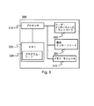
図1は、本願発明の種々の実施形態が適用することができるシステム100のいくらかの詳細を示す。このシステムは、例えば、ユーザ装置、ユーザ機器(UE)、および、メモリ・モジュール120のような外部ホスト110を含む。加えて、システムは、ホスト110とメモリ・モジュール120との間のデータ、制御信号およびクロック信号を通信するためのインタフェース130を備える。
FIG. 1 shows some details of a
メモリ・モジュール120は、たとえば、メモリー・カード、マルチ・メディア・カード(MMC:Multi Media Card)、セキュア・デジタル(SD)カード、あるいは、埋め込みメモリを備えることができる。メモリ・モジュール120は、メモリ・コントローラ121および、少なくとも1つのメモリ・デバイス122を備えることができる。メモリ・デバイス122は、データを格納するための複数のセクタを有するメモリ・ブロックを備えることができる。メモリ・コントローラ120は、ホスト・デバイス110との通信を容易にするためのホスト・インタフェース・コントローラ123、メモリ・デバイス122やメモリ・メンテナンス・コントローラ125との通信、および、動作(例えば、読み取り、書き込み、消去操作)を容易にするためのメモリ・インタフェース・コントローラ124を備えることができる。実施形態においては、コントローラ121、123−125は論理回路であることができる。
The
実施形態においては、メモリ・モジュール120がホスト(電子)デバイス110に接続しているとき、ホスト・コントローラ113は、インタフェース130を介して、ホスト・インタフェース・コントローラ123へコマンド信号を提供することができる。メモリ・デバイス122において、例えば、ファイルのようなデータ・エンティティは、メモリ・デバイス122の少なくとも2つのセクタを使って格納される。
In an embodiment, when the
実施形態においては、セクタは、
− 消去ブロック(NAND)、
− 書き込みブロック(eMMC)、
− ページ(NAND)、
− スーパー・ページ(ページのセット)、
−(例えば、ハードディスクの)セクタ
のうちの少なくとも1つを備えることができる。
In an embodiment, the sector is
-Erase block (NAND),
-Writing block (eMMC),
-Page (NAND),
-Super page (set of pages),
It may comprise at least one of the sectors (eg of a hard disk).
よりよく区別するために、大きなシーケンシャル操作と小さなランダム操作との間で、また、マルチタスキングのサポートを改善するために、コンテキストは、読込み、または、書込みコマンドのグループと結びついていることができる。コマンドのグループを単一のコンテキストと結びつけることは、このデバイスが、データのハンドリングを最適化することを許容する。断片化したセクタを消去するために、より速いソリューションもまた、必要である。 To better distinguish, context can be associated with groups of read or write commands between large sequential operations and small random operations, and to improve multitasking support . Combining a group of commands with a single context allows the device to optimize data handling. A faster solution is also needed to erase fragmented sectors.
コンテキストは、特定の読取り・書込みパターン(例えば、ある粒状度でシーケンシャルな)に対して構成されたアクティブなセッションとみることができる。マルティプルな読込みまたは書込みコマンドは、デバイスにパフォーマンスを最適化することを許容するために、それらの間のある論理的関係をつくる、このコンテキストと結びついている。例えば、大きなシーケンシャル書込みパターンは、デバイスが、内部の局所性を改善し、いくらかのオーバーヘッドを減少することを許容することによって、より良いパフォーマンスを有することができる。(例えば、データのある大規模ユニットが、書き込みが実行されている間の全体として電源異常に影響を受けることが許容されるならば、このユニットを満たすすべてのコマンドは、より速く動作することができる。電源異常の場合には通常、個々の書き込みを各々保護することが要求されるオーバーヘッドを減らすことができるからである。) A context can be viewed as an active session configured for a particular read / write pattern (eg, sequential with a certain granularity). Multiple read or write commands are associated with this context, which creates some logical relationship between them to allow the device to optimize performance. For example, a large sequential write pattern can have better performance by allowing the device to improve internal locality and reduce some overhead. (For example, if a large unit with data is allowed to be affected by a power failure as a whole while a write is being performed, all commands that satisfy this unit can run faster. (In the case of a power failure, it is usually possible to reduce the overhead required to protect each individual write.)
デバイスは、1つ以上の並列のコンテキストをサポートすることができ、これは、コンテキスト識別子(コンテキストID)によって識別される。コンテキストを使用するために、利用できるコンテキストIDが選択される。つぎに、それは、構成レジスタに書き込むことによって初期化される。すると、読取り・書込みコマンドを送る前に、コマンドにおけるコンテキストIDを指定することによってそのコンテキストに関連して、データを、読取り・書込みすることができる。そのコンテキストがもはや使用されないとき、コンテキストIDを閉じるために、構成レジスタは更新されなければならない。コンテキストは、別の構成/使用のためにそれを変更する前に、閉じられなければならない。 A device can support one or more parallel contexts, which are identified by a context identifier (context ID). In order to use the context, an available context ID is selected. It is then initialized by writing to the configuration register. Then, before sending a read / write command, data can be read / written in relation to that context by specifying the context ID in the command. When that context is no longer used, the configuration register must be updated to close the context ID. The context must be closed before changing it for another configuration / use.
実施形態においては、例えば、セクタのようなメモリ・デバイス・ロケーションは、ポインターを使用して示すことができる。このポインターは、たとえば、メモリ・デバイス・ロケーションの論理アドレスまたは物理アドレスを含むことができる。 In an embodiment, a memory device location, such as a sector, can be indicated using a pointer. This pointer can include, for example, a logical or physical address of the memory device location.
メモリ・モジュール120のメモリ・コントローラ121において、コンテキスト情報は、データ・エンティティについて維持されることができる。コンテキスト情報は、メモリ・デバイス122の少なくとも2つのセクタの論理アドレスを含むことができる。メモリ・コントローラ121において、信号を、少なくとも2つのセクタをメモリ・デバイス122から消去することを示すように規定することができる。メモリ・デバイス122の少なくとも2つのセクタは、つぎに、コンテキスト情報を使って消去することができる。
In the
ここに記載されたように、ホスト110から受信される信号は、少なくとも2つのセクタに含まれる、メモリ・デバイス122から消去されるデータ・エンティティのためのコンテキストIDを含むことができる。コンテキストIDは、ポインターを備えているコンテキスト情報を識別する。ポインターは、メモリ・デバイス122の第1のセクタの論理アドレスを示す開始アドレスと、メモリ・デバイス122の第2のセクタの論理アドレスを示す開始アドレスとを備えることができる。データ・エンティティの消去は、そのデータ・エンティティまたは、そのデータ・エンティティに関係するデータを含む少なくとも1つのセクタに関するデータを含むすべてのセクタを消去することを含むことができる。
As described herein, the signal received from the
実施形態においては、消去は、
− ERASE (eMMC)、
− TRIM(eMMC/ATA)、
− SecureTRIM/SecureERASE(eMMC)、
− DISCARD(eMMC)、
− Sanitize (eMMC)、
− Unmap (UFS)
機能のうちの少なくとも1つを使ってインプリメントすることができる。
In an embodiment, erasure is
-ERASE (eMMC),
-TRIM (eMMC / ATA),
-SecureTRIM / SecureERASE (eMMC),
-DISCARD (eMMC),
-Sanitize (eMMC),
-Unmap (UFS)
It can be implemented using at least one of the functions.
実施形態においては、消去可能な単位は、消去グループとして規定することができる。この消去グループは、書き込みブロックにおいて測定される。それは、基本的な書き込み可能な単位である。消去グループのサイズは、デバイスに特有のパラメータである。明示的に消去されたメモリ範囲のコンテンツは、異なるメモリ技術に依存して、「0」または「1」である。ERASEコマンドが正常に完了すると、消去されたマップされたデバイス・アドレス範囲は、異なるメモリ技術に依存して、すべて「0」または、すべて「1」で上書きされたかのようにふるまう。ERASEコマンドの影響は、単にマップされたホスト・アドレス範囲を、マップされていないホスト・アドレス範囲へ動かすことである。ホストは、Eraseグループの隣接する範囲を消去することができる。消去プロセスを始めることは、3つのステップのシーケンスである。まず、ホストは、ERASE_GROUP_STARTコマンドを用いて、その範囲の開始アドレスを規定し、次に、ERASE_GROUP_ENDコマンドを用いて、その範囲の最終アドレスを規定する。最後に、ゼロにセットする引数ビットを有するERASEコマンドを発行することによって、それは消去プロセスを始める。eraseコマンドのアドレス・フィールドは、バイト単位で、2GBまでの密度、セクタ単位で、2GBより大きい密度に対する消去グループアドレスである。 In the embodiment, the erasable unit can be defined as an erasure group. This erase group is measured in the write block. It is a basic writable unit. The size of the erase group is a parameter specific to the device. The contents of the explicitly erased memory range are “0” or “1” depending on the different memory technology. Upon successful completion of the ERASE command, the erased mapped device address range behaves as if it was overwritten with all “0” s or all “1” s, depending on the different memory technology. The effect of the ERASE command is simply to move the mapped host address range to an unmapped host address range. The host can erase the adjacent range of the Erase group. Starting the erase process is a three step sequence. First, the host uses the ERASE_GROUP_START command to define the start address of the range, and then uses the ERASE_GROUP_END command to define the final address of the range. Finally, it starts the erase process by issuing an ERASE command with an argument bit set to zero. The address field of the erase command is an erase group address for a density of up to 2 GB in bytes and a density greater than 2 GB in sectors.
実施形態においては、トリミング機能TRIMは、上述のERASE機能と同様である。その機能は、グループを消去する代わりに、ブロックを書き込むために消去動作を適用する。トリミング機能TRIMは、ホストが、もはや要求されないデータを識別し、バックグラウンド消去イベントの間に、必要に応じてデータを消去することを許容する。トリム機能が適用される書き込みブロックのコンテンツは、異なるメモリ技術に依存して、「0」または「1」であることができる。 In the embodiment, the trimming function TRIM is the same as the above-described ERASE function. The function applies an erase operation to write the block instead of erasing the group. The trim function TRIM allows the host to identify data that is no longer required and to erase the data as needed during a background erase event. The content of the write block to which the trim function is applied can be “0” or “1” depending on different memory technologies.
トリミング機能が正常に完了すると、トリミングされたマップされたデバイス・アドレス範囲は、異なるメモリ技術に依存して、すべて「0」または、すべて「1」で上書きされたかのようにふるまう。TRIMコマンドの影響は、単にマップされたホスト・アドレス範囲を、マップされていないホスト・アドレス範囲へ動かすことである。TRIMプロセスを完了することは、3つのステップのシーケンスである。まず、ホストは、ERASE_GROUP_STARTコマンドを用いた範囲の開始アドレスを規定することができ、次に、ERASE_GROUP_ENDコマンドを用いて範囲の最終アドレスを規定し、最後に、引数ビット0を、1にセットし、そして、引数の残りをゼロにセットして、ERASEコマンドを発行することにより消去プロセスを開始する。 Upon successful completion of the trimming function, the trimmed mapped device address range behaves as if it was overwritten with all “0” s or all “1” s, depending on different memory technologies. The effect of the TRIM command is simply to move the mapped host address range to an unmapped host address range. Completing the TRIM process is a three step sequence. First, the host can specify the start address of the range using the ERASE_GROUP_START command, then specify the final address of the range using the ERASE_GROUP_END command, and finally set the argument bit 0 to 1. Then, the erase process is started by setting the rest of the arguments to zero and issuing an ERASE command.
実施形態においては、SANITIZE機能を、デバイスからデータを取り除くために用いることができる。SANITIZE操作の使用は、デバイスにマップされていないユーザ・アドレス空間から物理的にデータを取り除くことを要求する。SANITIZE操作が完了されたあと、マップされていないホスト・アドレス空間には、データが存在してはならない。操作されている領域は、ホストによりアクセスできないので、この特徴を要求しているアプリケーションは、個々のデバイス・メーカーとともに、この操作が、適切に実行されることを確実とし、デバイス信頼性に対するインパクトを理解するために、機能しなければならない。 In embodiments, the SANITIZE function can be used to remove data from the device. Use of the SANITIZE operation requires that data be physically removed from the user address space that is not mapped to the device. After the SANITIZE operation is completed, there must be no data in the unmapped host address space. Since the area being manipulated is not accessible by the host, applications that require this feature, along with individual device manufacturers, ensure that this operation is performed properly and have an impact on device reliability. It must work to understand.
実施形態においては、DISCARD機能は、消去のために使用することができる。DISCARDは、TRIMと同様の操作である。DISCARD機能は、ホストが、バックグラウンド消去イベントの間に、デバイスが必要に応じてデータを消去することができるように、もはや要求されないデータを識別することを許容する。DISCARD機能が適用される書き込みブロックのコンテンツは、「ドント・ケア」となる。DISCARD操作の後、オリジナルデータは、部分的に、あるいは、完全に、デバイスに依存するままにすることができる。デバイスは、廃棄された書き込みブロックのコンテンツを決定する。DISCARDとTRIMの区別は、デバイスが、ホストは、読込み操作が指示されるときに、消去としてマークされた1つ以上の論理的ブロック・アドレスからオリジナルデータを取り出さないことを保証することを要求されない、装置の動作である。TRIMは、異なるメモリ技術に依存して、「0」か「1」によって応答する。廃棄プロセスを始めることは、3つのステップのシーケンスである。まず、ホストは、ERASE_GROUP_STARTコマンドを用いて、その範囲の開始アドレスを規定し、次に、ERASE_GROUP_ENDコマンドを用いて、その範囲囲の最終アドレスを規定する。最後に、1にセットされる引数ビット0およびビット1、および、ゼロにセットされる引数の残りを有するERASEコマンドを発行することによって、それは消去プロセスを始める。DISCARD操作の場合には、そのコマンドは、消去グループよりはむしろ書き込みブロックのアドレスを識別することができる。 In an embodiment, the DISCARD function can be used for erasure. DISCARD is the same operation as TRIM. The DISCARD function allows the host to identify data that is no longer required so that the device can erase data as needed during a background erase event. The content of the writing block to which the DISCARD function is applied is “don't care”. After the DISCARD operation, the original data can remain partially or completely device dependent. The device determines the contents of the discarded write block. The distinction between DISCARD and TRIM does not require the device to ensure that the host does not retrieve original data from one or more logical block addresses marked as erased when a read operation is directed. The operation of the device. The TRIM responds with a “0” or “1” depending on the different memory technology. Starting the disposal process is a three step sequence. First, the host uses the ERASE_GROUP_START command to specify the start address of the range, and then uses the ERASE_GROUP_END command to specify the final address of the range. Finally, it initiates the erase process by issuing an ERASE command with argument bits 0 and 1 set to 1 and the remainder of the argument set to zero. In the case of a DISCARD operation, the command can identify the address of the write block rather than the erase group.
実施形態においては、SecureERASE機能を使用することができる。セキュアなパージを示すSecureERASEコマンドは、消去グループの上で実行することができる。セキュアな消去は、この消去グループにおけるデータだけにされるのではなく、別の消去グループにおけるこのデータのいかなるコピーおいても行われなければならない。このコマンドは、直ちに実行され、メモリ・デバイスは、必要なすべての消去グループがパージされるまで、ホストに、コントロールを返さない。1つの消去グループは、例えば、特定のNANDフラッシュにおいて消去することができる最小限のメモリ・ブロックである。 In an embodiment, the SecureERASE function can be used. A SecureERASE command indicating a secure purge can be executed on the erase group. Secure erasure must be done on any copy of this data in another erase group, not just on the data in this erase group. This command is executed immediately and the memory device does not return control to the host until all necessary erase groups have been purged. An erase group is, for example, a minimum memory block that can be erased in a specific NAND flash.
実施形態においては、SecureTRIM機能を使用することができる。SecureERASEと同様に、SecureTRIMコマンドは、消去グループではなく、書き込みブロックのうえで動作する。これを適切に取り扱うために、この操作は、2つのステップに分割されることができる。第1のステップは、第2のステップが呼び出される前に、ブロックの複数のセットに行うことができるセキュア・パージのブロックをマークする。第2のステップは、すべての要求されたセキュア・トリミングを実行する別のビット・フラグシーケンスによる消去である。 In an embodiment, the SecureTRIM function can be used. As with SecureERASE, the SecureTRIM command operates on the write block, not the erase group. In order to handle this properly, this operation can be divided into two steps. The first step marks a block of secure purge that can be performed on multiple sets of blocks before the second step is called. The second step is an erasure with another bit flag sequence that performs all the required secure trimmings.
メモリ・デバイス122のセクタを消去することは、例えば、本願発明の実施形態にしたがうホスト110によって利用されることができる。ここに記載されたように、メモリ・メンテナンス・コントローラ125は、可能性がある消去セクタまたはブロックを備えるメモリ・メンテナンスを管理することができる。ファイル・アロケーション・テーブル(FAT)からファイル・システム・レベルにおいてデータ・アイテムを削除した後に、ホスト110は、削除されたとしてマークされたすべてのセクタを収集すること、削除されたとしてマークされた複数のセクタを、できる限り、論理的ないし物理的に消去することを実行するようにさらに構成することができる。ホスト110は、また、ガーベッジ・コレクション削除した後のメモリ・デバイス122のメモリ損耗平均化を実行することもできる。さらには、メモリ・メンテナンス・コントローラ125は、ホストからの命令に基づいて、消去されるべきとマークされたすべてのセクタを収集すること、その複数のセクタを、できる限り、論理的ないし物理的に消去することを実行するようにさらに構成されることができる。ホスト110からの命令に基づいて、メモリ・メンテナンス・コントローラ125は、消去の後、メモリ・デバイス122のメモリ損耗平均化を実行することができる。
Erasing a sector of
実施形態においては、メモリ・コントローラ121、ホスト・インタフェース・コントローラ123、メモリ・デバイス・コントローラ124、メモリ・メンテナンス・コントローラ125、および、メモリ・デバイス122は、ソフトウェアモジュール、ハードウェアモジュールまたはその組合せとしてインプリメントすることができる。さらには、モジュール121−125の各々は、別々のモジュール/ブロックとしてインプリメントされることができる、あるいは、メモリ・モジュール120の任意の他の標準モジュール/ブロックとも結合することができる、あるいは、それらの機能性によって、数ブロックに分けることができる。すべての、または、選択したメモリ・モジュール120のモジュール/ブロックは、1つの集積回路を使ってインプリメントすることができる。
In the embodiment, the
実施形態においては、図1に示されるレジスタ126は、以前に記載された構成レジスタ等のレジスタ情報を格納するように構成される。レジスタ126は、例えば、メモリ・デバイス122に位置することもできる、レジスタは、メモリ・コントローラ121によってアクセスされることができる。
In an embodiment, the
図2は、本願発明の種々の実施形態が適用することができるメモリ・デバイス122のいくつかの詳細を示す。
FIG. 2 illustrates some details of the
実施形態においては、ファイル・システム・インプリメンテーションにおいて、データは、例えば、メモリ・デバイスへ書き込まれ、そして、新しいデータは、古いものに上書きするだけである。ファイルは、ファイル/クラスタ/セクタ・エントリを、「予約されていない」と書き込むことによって、ファイル・アロケーション・テーブル(FAT)から削除されるだけである。データをメモリ・デバイスから消去することは、別の機能である。 In an embodiment, in a file system implementation, data is written to, for example, a memory device, and new data only overwrites old ones. The file is only deleted from the file allocation table (FAT) by writing the file / cluster / sector entry as “not reserved”. Erasing data from the memory device is another function.
論理インタフェースを介して、フラッシュ・メモリにデータを書き込むときに、ホストは、典型的には、メモリ・システムの連続仮想アドレス空間の中で、ユニークな論理アドレスを、セクタに、クラスタまたはデータの他の単位に割り当てる。ホストは、ファイル・システムを典型的には維持し、ファイルデータを論理的クラスタに割り当てる。ここで、クラスタ・サイズは、典型的には固定である。フラッシュ・デバイスは、複数論理セクタに分割され、ホストは、複数の論理セクタを備えるクラスタの中に、スペースを割り当てる。クラスタは、論理アドレスの細区分であり、クラスタ・マップは、ファイル・アロケーション・テーブル(FAT)として指定されることができる。ファイル・アロケーション・テーブル(FAT)は、通常、格納デバイス自体の上に格納される。 When writing data to flash memory via a logical interface, the host typically assigns a unique logical address, sector, cluster or other data within the contiguous virtual address space of the memory system. Assign to units. The host typically maintains a file system and assigns file data to logical clusters. Here, the cluster size is typically fixed. The flash device is divided into multiple logical sectors, and the host allocates space in a cluster comprising multiple logical sectors. A cluster is a subdivision of logical addresses, and a cluster map can be specified as a file allocation table (FAT). The file allocation table (FAT) is usually stored on the storage device itself.
連続論理アドレス空間は、メモリ・デバイス122の中に格納することができるデータのすべてに対してアドレスを提供するのに十分大きい。ホスト・アドレス空間は、セクタのインクリメントまたはデータのクラスタに、典型的には分割される。各々のクラスタは、所与のホストシステムにおいて、データのいくつかのセクタ、だいたい、典型的には、4つのセクタと64のセクタとの間のセクタを含むように設計されることができる。標準的なセクタは、例えば、512または4096バイトのデータを含む。
The contiguous logical address space is large enough to provide an address for all of the data that can be stored in the
図2は、典型的には、メモリ・デバイス122がどのように分割されるかの例を示す。格納デバイス122は、複数の分割を含むことができる。そして、図2においては、単一の分割210が、単純さのために示される。分割210は、システム領域220とデータエリア230とを含む。システム領域220は、種々のセグメント、例えば、マスター・ブート・レコード(「MBR」)領域、分割ブート・レコード(「PBR」)領域、FAT1領域、FAT2領域、および、ルート・ディレクトリ領域を有する。
FIG. 2 typically shows an example of how the
MBR領域は、全体的な分割情報を格納し、媒体がブート可能なデバイスである場合には、MBRは、MBR領域からPBR領域にジャンプする命令を含む。MBR領域も、隠された領域を含み、それはMBR領域とPBR領域との間の予約スペースである。 The MBR area stores overall partition information, and if the medium is a bootable device, the MBR includes an instruction to jump from the MBR area to the PBR area. The MBR area also includes a hidden area, which is a reserved space between the MBR area and the PBR area.
PBR領域は、分割に対する分割/ブート情報を含む。例えば、PBR領域は、ファイル・アロケーション・テーブル(FAT)(たとえば、12/16/32ビット)のタイプ、ラベル(すなわち、ドライブの名前)、ドライブの寸法、クラスタ・サイズ(すなわち、アロケーションユニットごとのセクタの数)、多くのファイル・アロケーション・テーブル(FAT)領域、(図(2)に示される2つのFAT領域、FAT1およびFAT2)、および、ファイル・アロケーション・テーブル(FAT)ごとのセクタ数に対する情報を含む。ファイル・アロケーション・テーブル(FAT)領域は、各々のファイルに対するセクタ/クラスタ情報を含む。例えば、FAT−12に対して、ファイル・アロケーション・テーブル(FAT)域における各々のエントリは12ビットを含み、そして、合計で4096のエントリがある。ルート・ディレクトリは、各々のファイルに対するエントリを含む。各々のディレクトリ・エントリは、ファイル名またはディレクトリに対する特定数のバイト(たとえば、8バイト)、拡張のためのいくつかのバイト(たとえば、3バイト)、ファイル属性(たとえば、ファイルがリードオンリーであるか、隠されているか、システムファイルであるか、ボリュームラベルであるか、ディレクトリであるか、修正されたものであるか、など)に対して、いくつかのバイト(たとえば、1バイト)、ファイルが作成されたときの日時を示しているいくつかのバイト、開始セクタ/クラスタに対する特定数のバイト数(たとえば、2)、および、ファイルの長さを示している特定数のバイト(たとえば4)を含む。開始セクタ/クラスタに対するいくつかのバイトは、ファイル・アロケーション・テーブル(FAT)における第1のセクタ/クラスタを指しており、終了セクタ/クラスタは、例えば、0xFFFまたは0Xffffffにより、示すことができる。 The PBR area includes split / boot information for the split. For example, the PBR area is the file allocation table (FAT) (eg, 12/16/32 bit) type, label (ie, drive name), drive size, cluster size (ie, per allocation unit) Number of sectors), many file allocation table (FAT) areas (two FAT areas shown in Figure (2), FAT1 and FAT2), and the number of sectors per file allocation table (FAT) Contains information. The file allocation table (FAT) area contains sector / cluster information for each file. For example, for FAT-12, each entry in the file allocation table (FAT) area contains 12 bits and there are a total of 4096 entries. The root directory contains an entry for each file. Each directory entry has a specific number of bytes for the file name or directory (eg, 8 bytes), several bytes for extension (eg, 3 bytes), file attributes (eg, whether the file is read only) , Hidden, system file, volume label, directory, modified, etc.) for some bytes (eg 1 byte), the file A number of bytes indicating the date and time when it was created, a specific number of bytes for the starting sector / cluster (eg 2), and a specific number of bytes indicating the length of the file (eg 4) Including. Several bytes for the starting sector / cluster point to the first sector / cluster in the file allocation table (FAT), and the ending sector / cluster can be indicated by, for example, 0xFFF or 0Xffffff.
ディレクトリにファイル名を書き込むために、ホストシステムは、フリーのセクタ/クラスタ・スペースをFAT1領域で見つけ、データが、データエリア230で書き込まれる。FAT1およびFAT2のエントリの両方が、つぎに、更新される。ディレクトリ・エントリ、すなわち、日付/時間/開始セクタ/クラスタ/ファイル長も、また更新される。
To write a file name to the directory, the host system finds free sector / cluster space in the FAT1 area and the data is written in the
実施形態においては、データ・エンティティ、たとえば、ファイル、は、パーティション210において、メモリ・デバイス122に格納される。データ・エンティティは、2つのセクタ231、232に格納される。コンテキスト構成を、このデータ・エンティティに対して規定することができ、コンテキストIDによって識別される。構成は、要求された特定のコンテキストIDの構成レジスタに書き込むことによって、なされることができる。つぎに、このコンテキストIDに結びついているすべての読み出しコマンド、または、書き込みコマンドは、そのIDとともに送られる。そのコンテキストが、もはや必要でないとき、それは、「0」バイトを、構成レジスタへ書き込むことによって閉じなければならない。この構成レジスタは、例えば、各コンテキスト(固定、定義済み#0を除いて)につき1つの15バイト・レジスタのアレイである。異なる規則は、また、同じファイル/コンテキストIDに後ほど追加される新しいデータに対して規定することができる。構成レジスタのIDインデックスは、それを閉じた後に再開することができ、IDインデックスは、常に、新しいエンティティをつくることができる。しかしながら、データがIDインデックスへうまく書き込まれて、コンテキストIDは閉じられたあとに、データは、論理的にグループ化される。ホストに対する、このグループの露出はないが、しかし、メモリ・コントローラは、NANDの予備のページから、例えば、ページまたは格納データのヘッダを見つけ出すための手段を有する。
In an embodiment, data entities, eg, files, are stored in
実施形態においては、ホストは、例えば、ファイルのようなデータ・エンティティを削除することに決める。ホスト・アプリケーションから削除信号を受信することに応じて、ホストは、ファイル・アロケーション・テーブル(FAT)において、フリーとして、対応するアロケーションを、マークするさらには、メモリ・デバイスのセクタ231、232に位置するデータ・エンティティを消去することは、また、望ましいことである。セクタ231、232は、セクタ231、232に対して別々のトリミング機能を使用して、消去することができる。
In an embodiment, the host decides to delete a data entity such as a file. In response to receiving a delete signal from the host application, the host marks the corresponding allocation as free in the file allocation table (FAT), and is further located in
実施形態においては、複数のセクタに含まれるファイルを消去するための、より効率的な方法がホストからメモリ・デバイスに複数のトリミング・コマンドを送ることのオーバーヘッドを減らすことによって、導入される。メモリ・コントローラは、データ・エンティティ(ファイル)の特定の部分が、互いに属しており、特定の単一のトリミング機能は、全体としてそのようなデータに適用するように規定することができることを通知され得る。そのような機能は、そのファイルでおおわれるセクタの数/アドレスから独立している。コンテキストIDの機能は、例えばファイルなど、データ・エンティティを備えているセクタ231、232を消去するために使用することができる。少なくとも、次のようなオプションが存在することができる。
In an embodiment, a more efficient method for erasing files contained in multiple sectors is introduced by reducing the overhead of sending multiple trimming commands from the host to the memory device. The memory controller is informed that certain parts of the data entity (file) belong to each other and a specific single trimming function can be defined to apply to such data as a whole obtain. Such a function is independent of the number / address of sectors covered by the file. The context ID function can be used to erase
第1のオプションは、特定のコンテキストID消去機能を導入することである。別々の特定のコマンド、あるいは、既存のコマンドにおける特別なパラメータを、使用することができる。さらには、レジスタの設定を用いることができる。第1のオプションは、既存の消去機能をそのまま利用することができる。そのような消去機能は、また、特定のデータ・エンティティの単一のセクタ、IDまたはファイルを消去するために使用することもできる。消去機能は、例えば、JEDEC eMMCおよびUFSメモリ標準の、Erase、SecureErase、TRIM、SecureTRIM、または、Discardコマンドを備えることができる。 The first option is to introduce a specific context ID deletion function. Separate specific commands or special parameters in existing commands can be used. Furthermore, register settings can be used. The first option can use the existing erase function as it is. Such an erase function can also be used to erase a single sector, ID or file of a particular data entity. The erase function may comprise, for example, JEDEC eMMC and UFS memory standard Erase, SecureErase, TRIM, SecureTRIM, or Discard commands.
第2のオプションは、消去機能により用いられるコンテキストIDのアドレスを導入することである。消去機能は、開始アドレスまたは、コンテキストIDのどんなアドレスでも使うことができ、そして、自動的に、同じコンテキストIDに属しているすべてのセクタを消去する。 The second option is to introduce the address of the context ID used by the erase function. The erase function can use either the start address or any address of the context ID and automatically erases all sectors belonging to the same context ID.
第3のオプションは、階層的な消去機能を導入することである。コンテキストは、他のコンテキストIDのスーパーセットを提供しているコンテキストIDに対応する他のコンテキストのスーパーセットを含むことができる。そのような階層は、コンテキストID1へ書き込まれるデータが例えば、データベースであり、コンテキストID2へ書き込まれるデータがID1データベースのアイテムであることを可能にすることができる。結局、ID2のアドレスへの単一のトリミング・コマンドは、このアイテムに属しているセクタの位置がどんなに断片的であっても、このアイテムをデータベースから無効にすることができ、消去することができる。さらには、ID1のアドレスへの単一のトリミング・コマンドは、全部のデータベース、また、ID2に当初書き込まれたもの以外のそれに属しているすべてのアイテムを無効にすることができる、また、インデックスの階層に関係する制御レジスタも存在する。 A third option is to introduce a hierarchical erase function. A context may include a superset of other contexts corresponding to a context ID providing a superset of other context IDs. Such a hierarchy can allow data written to context ID1 to be a database, for example, and data written to context ID2 to be an item of an ID1 database. Eventually, a single trim command to ID2's address can invalidate and delete this item from the database, no matter how fragmentary the sector's position belongs to this item. . Furthermore, a single trim command to the address of ID1 can invalidate the entire database and all items belonging to it other than those originally written to ID2, and the index There are also control registers related to the hierarchy.
図3は、本願発明の種々の実施形態が適用することができるユーザ装置300の例のブロック図を提示する。これは、例えば、移動端末、ラップトップ、タブレット、または、他の通信装置のようなユーザ機器(UE)、ユーザ・デバイスまたは装置、であることができる。
FIG. 3 presents a block diagram of an
ユーザ装置300の一般的な構成は、通信インタフェース・モジュール350、通信インタフェース・モジュール350に結合されたプロセッサ310、および、プロセッサ310に結合されたメモリ320を備える。ユーザ装置は、更に、メモリ・320における格納されたソフトウェア330を備え、プロセッサ310へロードされて、実行されるように動作可能である。ソフトウェア330は、1つ以上のソフトウェアモジュールを含むことができ、コンピュータ・プログラム・プロダクトの形であることができる。ユーザ装置300は、更に、プロセッサ310に結合されたユーザー・インターフェース・コントローラ360を備える。
The general configuration of the
通信インタフェース・モジュール350は、本願発明の種々の実施形態に関連して議論されたユーザ・データ・ラジオの少なくとも部分的にインプリメントする。通信インタフェース・モジュール350は、例えば、WLAN、ブルートゥース(Bluetooth(登録商標))、GSM/GPRS、CDMA、WCDMA、または、LTE(Long Term Evolution)無線モジュールのようなラジオ・インタフェース・モジュールであることができる。通信インタフェース・モジュール350は、ユーザ装置300に、または、アダプタ、カードまたは、ユーザ装置300の適当なスロットまたはポートに挿入することができるような他のものに統合化することができる。通信インタフェース・モジュール350は、1つのラジオ・インタフェース技術または複数のテクノロジーをサポートすることができる。図3は、1つの通信インタフェース・モジュール350を示すが、しかし、ユーザ装置300は、複数の通信インタフェース・モジュール350を備えることできる。
プロセッサ310は、例えば、中央処理装置(CPU)、マイクロプロセッサー、デジタルシグナルプロセッサ(DSP)、グラフィック処理装置、その他であることができる。図3は、1つのプロセッサ310を示すが、しかし、ユーザ装置300は、複数のプロセッサを備えることができる。
The
メモリ・320は、たとえば、読取り専用メモリ(ROM)、プログラム可能読取り専用メモリ(PROM)、消去可能・プログラム可能読取り専用メモリ(消去可能PROM)、ランダム・アクセスで・メモリ(RAM)、フラッシュ・メモリ、データ・ディスク、光学ストレージ、磁気ストレージ、スマート・カード、その他のような不揮発性あるいは揮発性メモリであることができる。ユーザ装置300は、複数のメモリを備えることができる。メモリ320は、装置300の一部として構築することができる。あるいは、それは、ユーザによって、スロット、ポート、または、ユーザ装置300のその他に挿入することができる。メモリ320は、データを格納するという唯一の目的に、役立つことができる、または、それは、例えば、データ処理など他の目的に役立つ装置の一部として構成することができる。
メモリ・モジュール340は、ユーザ装置300で使われるスマート・カードとして含まれることができる。メモリ・モジュールは、たとえば、読取り専用メモリ(ROM)、プログラム可能読取り専用メモリ(PROM)、消去可能・プログラム可能読取り専用メモリ(消去可能PROM)、ランダム・アクセスで・メモリ(RAM)、フラッシュ・メモリ、データ・ディスク、光学ストレージ、磁気ストレージ、スマート・カード、その他のような不揮発性あるいは揮発性メモリであることができる。ユーザ装置300は、複数のメモリ・モジュール340を備えることができる。メモリ・モジュール340は、ユーザによって、スロット、ポート、または、ユーザ装置300のその他に挿入することができる。メモリ340は、データを格納するという唯一の目的に、役立つことができる、または、それは、例えば、データ処理など他の目的に役立つ装置の一部として構成することができる。
The
ユーザ・インターフェース・コントローラ360は、ユーザ装置300のユーザから、例えば、キーボード、ユーザ装置300のディスプレイの上で示されるグラフィカル・ユーザ・インタフェース、音声認識回路、または、例えば、ヘッドセットのようなアクセサリー・デバイスを介して、入力を受信するための回路、および、ユーザに対して、例えば、グラフィカル・ユーザ・インタフェースまたは、ラウド・スピーカを介して出力を提供するための回路を備えることができる。
The
当業者は、図3に示される要素に加えて、ユーザ装置300は、たとえば、入出力(I/O)回路、メモリー・チップ、特定用途向け集積回路(ASIC)、ソースコーディング/デコーディング回路のような特定の目的のための処理回路、チャネルコーディング/デコーディング回路、暗号化/暗号解読回路、など追加的な回路とならんで、例えば、マイクロフォン、ディスプレイなど他の要素を備えることができることを理解する。加えて、ユーザ装置300は、外部電源もしも外部電源供給が利用できないときに、ユーザ装置300を動かすための使い捨て、または充電式電池(図示せず)を含むことができる。
Those skilled in the art will appreciate that in addition to the elements shown in FIG. 3,
図4は、本願発明の例の実施形態に従って、メモリ・モジュールにおける動作を示すフローチャートを示す。ステップ400において、この方法は、開始する。ステップ410において、データ・エンティティは、メモリ・デバイスの少なくとも2つのセクタを使って格納され、この少なくとも2つのセクタは、同一のデータ・エンティティに結びついている。ステップ420において、メモリ・モジュールのメモリ・コントローラにおいて、このメモリ・デバイスの少なくとも2つのセクタのうちの少なくとも1つへのポインターを含むデータ・エンティティのコンテキスト情報が、維持される。ステップ430において、メモリ・コントローラにおいて、信号を、少なくとも2つのセクタを、メモリ・デバイス122から消去することを示すように規定する。ステップ440において、このメモリ・デバイスの少なくとも2つのセクタは、コンテキスト情報を使って消去される。ステップ450において、この方法は終了する。
FIG. 4 shows a flow chart illustrating operation in a memory module, according to an example embodiment of the present invention. In
種々の実施形態は提示された。この文書において、単語は、除外する意図がないオープン・エンドな表現を備え、含み、相当し、そのようなものとして用いられていることは理解されるべきである。 Various embodiments have been presented. In this document, it is to be understood that words are used as such, with and including open-ended expressions that are not intended to be excluded.
前述の説明は、本願発明の特定のインプリメンテーションと実施形態の非限定的な例として、本願発明を実行するための現在、発明者によって考えられるベスト・モードの完全で有益な説明を提供した。しかしながら、本願発明は、上で提示された実施形態の詳細に制限されず、同等の手段を用いて、または、実施形態の異なる組合せにより、本願発明の特性からそれることなく、他の実施形態においてインプリメントすることができることは、当業者には明らかである。 The foregoing description provided a complete and informative description of the best mode currently contemplated by the inventors for carrying out the invention as a non-limiting example of specific implementations and embodiments of the invention. . However, the present invention is not limited to the details of the embodiments presented above, other embodiments using equivalent means or by different combinations of the embodiments without departing from the characteristics of the present invention. It will be apparent to those skilled in the art that it can be implemented in
さらには、上で開示したこの発明の実施形態の特徴のいくつかは、他の特徴に対応したものを使用しなくても、優位なものとして使用することができる。したがって、前述の説明は、単に、本願発明の原理を説明するものであり、それらに、制限されるものではないと考えられるべきである。これゆえに、本願発明の範囲は、添付の特許請求の範囲によってのみ、制限されるものである。 Furthermore, some of the features of the embodiments of the invention disclosed above can be used as an advantage without using those corresponding to other features. Accordingly, the foregoing description is merely illustrative of the principles of the invention and should not be construed as limiting. Therefore, the scope of the present invention is limited only by the appended claims.
Claims (18)
メモリ・コントローラにおいて、前記メモリ・デバイスの前記少なくとも2つのセクタのうちの少なくとも1つへのポインターを含むデータ・エンティティのコンテキスト情報を維持するステップと、
前記コンテキスト情報を使用して、前記メモリ・デバイスの前記少なくとも2つのセクタを消去するステップと、
を含む方法。 Storing a data entity that uses at least two sectors of the memory device, the at least two sectors being associated with the same data entity;
Maintaining in the memory controller context information of a data entity that includes a pointer to at least one of the at least two sectors of the memory device;
Erasing the at least two sectors of the memory device using the context information;
Including methods.
前記少なくとも2つのセクタのうちの少なくとも1つを、前記ファイル・アロケーション・テーブルから前記データ・エンティティ・エントリの削除に対応して、メモリ・デバイスから、消去することを示す信号を生成するステップと
を更に含む請求項1または2に記載の方法。 Deleting a data entity entry from a file allocation table by a host in response to a delete signal from an external host application;
Generating a signal from the memory device indicating that at least one of the at least two sectors is to be erased in response to the deletion of the data entity entry from the file allocation table; The method according to claim 1 or 2, further comprising:
− TRIM、
− SecureTRIM、
− SecureERASE、
− DISCARD、
− Sanitize、
− Unmap(UFS)
のコマンドのうちの少なくとも1つを用いる消去機能によって、前記メモリ・デバイスの前記少なくとも2つのセクタを消去するステップを更に含む請求項1ないし9のいずれか1項に記載の方法。 -ERASE,
-TRIM,
-SecureTRIM,
-SecureERASE,
-DISCARD,
-Sanitize,
-Unmap (UFS)
10. A method according to any one of the preceding claims, further comprising erasing the at least two sectors of the memory device by an erase function using at least one of the commands.
− 消去ブロック、
− 書き込みブロック、
− ページ、
− スーパー・ページ、および
− ハードディスクのセクタ、
のうちの少なくとも1つを含む、請求項1ないし11のいずれか1項に記載の方法。 The sector is
-Erase block,
-Writing blocks,
− Page,
-Super pages, and-hard disk sectors,
The method according to claim 1, comprising at least one of the following:
外部ホストへの、および、前記少なくとも1つのメモリ・デバイスへのインタフェースを有するメモリ・コントローラと、
を備えるメモリ・モジュールであって、
前記メモリ・デバイスは、コンピュータ・プログラムコードを含み、
該コンピュータ・プログラムコードは、前記メモリ・コントローラを用いて、前記メモリ・モジュールに、
少なくとも、メモリ・デバイスの少なくとも2つのセクタを使用するデータ・エンティティを格納することであって、該少なくとも2つのセクタは、同一のデータ・エンティティに結びついている、ことと、
メモリ・コントローラにおいて、前記メモリ・デバイスの前記少なくとも2つのセクタのうちの少なくとも1つへのポインターを含むデータ・エンティティのコンテキスト情報を維持することと、
前記コンテキスト情報を使用して、前記メモリ・デバイスの前記少なくとも2つのセクタを消去することと、
をさせるように構成されている、メモリ・モジュール。 At least one memory device;
A memory controller having an interface to an external host and to the at least one memory device;
A memory module comprising:
The memory device includes computer program code;
The computer program code is stored in the memory module using the memory controller.
Storing at least a data entity that uses at least two sectors of the memory device, the at least two sectors being associated with the same data entity;
Maintaining in a memory controller data entity context information including a pointer to at least one of the at least two sectors of the memory device;
Erasing the at least two sectors of the memory device using the context information;
A memory module configured to cause
前記メモリ・コントローラにおいて、前記少なくとも2つのセクタのうちの少なくとも1つを、前記メモリ・デバイスから消去することを示す信号を規定すること
をさせるように更に構成されている、請求項13に記載のメモリ・モジュール。 The computer program code is at least stored in the memory module using the memory controller.
14. The memory controller of claim 13, further configured to cause the memory controller to define a signal indicating that at least one of the at least two sectors is to be erased from the memory device. Memory module.
前記ホストによって、外部ホスト・アプリケーションからの削除信号に応じて、ファイル・アロケーション・テーブルから、データ・エンティティ・エントリ削除することと、
前記少なくとも2つのセクタのうちの少なくとも1つを、前記ファイル・アロケーション・テーブルから前記データ・エンティティ・エントリの削除に対応して、メモリ・デバイスから、消去することを示す信号を生成することと
をさせるように更に構成されている、請求項13または14に記載のメモリ・モジュール。 The computer program code is at least stored in the memory module using the memory controller.
Deleting a data entity entry from the file allocation table by the host in response to a delete signal from an external host application;
Generating a signal from the memory device indicating that at least one of the at least two sectors is to be erased in response to the deletion of the data entity entry from the file allocation table; 15. The memory module according to claim 13 or 14, further configured to cause
− 埋め込み型マルチ・メディア・カード(eMMC:Embedded MultiMediaCard)、
− メモリー・カード(SD)、
− アドバンスト・テクノロジー・アタッチメント(ATA)、および
− ユニバーサル・フラッシュ・ストレージ(UFS:Universal Flash Storage)
のうちの少なくとも1つを含む、請求項13ないし16のいずれか1項に記載のメモリ・モジュール。 The memory module is
-Embedded multimedia card (eMMC: Embedded MultiMediaCard),
-Memory card (SD),
-Advanced Technology Attachment (ATA), and-Universal Flash Storage (UFS)
17. A memory module according to any one of claims 13 to 16, comprising at least one of:
該コンピュータ実行可能プログラムコードは、メモリ・モジュールの少なくとも1つのコントローラによって実行されるとき、該メモリ・モジュールに、
メモリ・デバイスの少なくとも2つのセクタを使用するデータ・エンティティを格納することであって、該少なくとも2つのセクタは、同一のデータ・エンティティに結びついている、ことと、
メモリ・コントローラにおいて、前記メモリ・デバイスの前記少なくとも2つのセクタのうちの少なくとも1つへのポインターを含むデータ・エンティティのコンテキスト情報を維持することと、
前記コンテキスト情報を使用して、前記メモリ・デバイスの前記少なくとも2つのセクタを消去することと、
をさせる、コンピュータ・プログラム。 A computer program embodied on a computer readable medium containing computer executable program code comprising:
When the computer-executable program code is executed by at least one controller of the memory module,
Storing a data entity that uses at least two sectors of the memory device, the at least two sectors being associated with the same data entity;
Maintaining in a memory controller data entity context information including a pointer to at least one of the at least two sectors of the memory device;
Erasing the at least two sectors of the memory device using the context information;
A computer program that lets you
Applications Claiming Priority (1)
| Application Number | Priority Date | Filing Date | Title |
|---|---|---|---|
| PCT/FI2011/051168 WO2013098463A1 (en) | 2011-12-29 | 2011-12-29 | Method for erasing data entity in memory module |
Publications (2)
| Publication Number | Publication Date |
|---|---|
| JP2015507798A true JP2015507798A (en) | 2015-03-12 |
| JP2015507798A5 JP2015507798A5 (en) | 2015-05-07 |
Family
ID=45531881
Family Applications (1)
| Application Number | Title | Priority Date | Filing Date |
|---|---|---|---|
| JP2014549505A Pending JP2015507798A (en) | 2011-12-29 | 2011-12-29 | Method for erasing data entities in a memory module |
Country Status (4)
| Country | Link |
|---|---|
| US (1) | US10048884B2 (en) |
| EP (1) | EP2798500A1 (en) |
| JP (1) | JP2015507798A (en) |
| WO (1) | WO2013098463A1 (en) |
Families Citing this family (11)
| Publication number | Priority date | Publication date | Assignee | Title |
|---|---|---|---|---|
| US9329990B2 (en) * | 2013-01-11 | 2016-05-03 | Micron Technology, Inc. | Host controlled enablement of automatic background operations in a memory device |
| US10445229B1 (en) | 2013-01-28 | 2019-10-15 | Radian Memory Systems, Inc. | Memory controller with at least one address segment defined for which data is striped across flash memory dies, with a common address offset being used to obtain physical addresses for the data in each of the dies |
| US9959072B2 (en) * | 2013-12-20 | 2018-05-01 | Sandisk Technologies Llc | Systems and methods of compressing data |
| US9286160B2 (en) | 2014-02-07 | 2016-03-15 | Stmicroelectronics S.R.L. | System and method for phase change memory with erase flag cells |
| KR102545166B1 (en) | 2016-07-26 | 2023-06-19 | 삼성전자주식회사 | Host and Storage System securely deleting files and Operating Method of Host |
| CN106599699B (en) * | 2016-11-01 | 2020-06-09 | 惠州Tcl移动通信有限公司 | Method and system for realizing safe deletion of data in mobile terminal |
| US10579288B2 (en) | 2017-08-31 | 2020-03-03 | Micron Technology, Inc. | Prioritized security |
| KR102411290B1 (en) | 2017-10-24 | 2022-06-22 | 삼성전자주식회사 | Storage system including host device and storage device configured to perform selective purge operation |
| CN111803915A (en) * | 2020-06-11 | 2020-10-23 | 深圳市谷粒科技有限公司 | Automatic learning file transmission method and device for gamepad |
| EP3922329B1 (en) * | 2020-06-11 | 2023-10-25 | Shenzhen Guli Tech Co., Ltd. | Self-learning file transmitting, data reading and writing, app communication reading and writing methods of game handle |
| JP2022147909A (en) * | 2021-03-24 | 2022-10-06 | キオクシア株式会社 | memory system |
Citations (3)
| Publication number | Priority date | Publication date | Assignee | Title |
|---|---|---|---|---|
| JPH1153248A (en) * | 1997-08-04 | 1999-02-26 | Tokyo Electron Ltd | Data processing system, block erasure type storage medium and program recording medium |
| JP2000076116A (en) * | 1998-08-31 | 2000-03-14 | Kano Densan Hongkong Yugenkoshi | Electronic device, control method therefor and storage medium |
| JP2007293917A (en) * | 1997-08-08 | 2007-11-08 | Toshiba Corp | Method for controlling memory system |
Family Cites Families (28)
| Publication number | Priority date | Publication date | Assignee | Title |
|---|---|---|---|---|
| US3534338A (en) | 1967-11-13 | 1970-10-13 | Bell Telephone Labor Inc | Computer graphics system |
| US5337275A (en) | 1992-10-30 | 1994-08-09 | Intel Corporation | Method for releasing space in flash EEPROM memory array to allow the storage of compressed data |
| US5809340A (en) | 1993-04-30 | 1998-09-15 | Packard Bell Nec | Adaptively generating timing signals for access to various memory devices based on stored profiles |
| JP4079506B2 (en) | 1997-08-08 | 2008-04-23 | 株式会社東芝 | Method for controlling nonvolatile semiconductor memory system |
| US6279114B1 (en) | 1998-11-04 | 2001-08-21 | Sandisk Corporation | Voltage negotiation in a single host multiple cards system |
| US6205494B1 (en) * | 1998-12-18 | 2001-03-20 | Western Digital Corporation | Controller with automatic generation of linked list of data transfer descriptors for sequential commands, with linked list being used for execution of sequential data transfers |
| US6681304B1 (en) | 2000-06-30 | 2004-01-20 | Intel Corporation | Method and device for providing hidden storage in non-volatile memory |
| EP1199723B1 (en) | 2000-10-18 | 2008-12-31 | STMicroelectronics S.r.l. | Interlaced memory device with random or sequential access |
| US7478248B2 (en) | 2002-11-27 | 2009-01-13 | M-Systems Flash Disk Pioneers, Ltd. | Apparatus and method for securing data on a portable storage device |
| DE60307798T2 (en) | 2003-05-30 | 2006-12-14 | Agilent Technologies, Inc., Palo Alto | Arbitration of shared memory |
| US7152801B2 (en) | 2004-04-16 | 2006-12-26 | Sandisk Corporation | Memory cards having two standard sets of contacts |
| US7395384B2 (en) * | 2004-07-21 | 2008-07-01 | Sandisk Corproation | Method and apparatus for maintaining data on non-volatile memory systems |
| JP2006343923A (en) | 2005-06-08 | 2006-12-21 | Fujitsu Ltd | Disk recording device |
| US7409489B2 (en) | 2005-08-03 | 2008-08-05 | Sandisk Corporation | Scheduling of reclaim operations in non-volatile memory |
| US20070079015A1 (en) | 2005-09-30 | 2007-04-05 | Intel Corporation | Methods and arrangements to interface a data storage device |
| WO2007058617A1 (en) * | 2005-11-17 | 2007-05-24 | Chee Keng Chang | A controller for non-volatile memories, and methods of operating the memory controller |
| CN100485681C (en) | 2006-03-23 | 2009-05-06 | 北京握奇数据系统有限公司 | Smart card storage system and managing method for file creation in the system |
| US7787870B2 (en) | 2006-09-29 | 2010-08-31 | Motorola, Inc. | Method and system for associating a user profile to a caller identifier |
| WO2008070803A1 (en) * | 2006-12-06 | 2008-06-12 | Fusion Multisystems, Inc. (Dba Fusion-Io) | Apparatus, system, and method for managing data from a requesting device with an empty data token directive |
| US8719501B2 (en) * | 2009-09-08 | 2014-05-06 | Fusion-Io | Apparatus, system, and method for caching data on a solid-state storage device |
| US8307180B2 (en) | 2008-02-28 | 2012-11-06 | Nokia Corporation | Extended utilization area for a memory device |
| WO2011095516A1 (en) * | 2010-02-05 | 2011-08-11 | St-Ericsson Sa | Method and system for mass storage on flash memory |
| US20120173795A1 (en) * | 2010-05-25 | 2012-07-05 | Ocz Technology Group, Inc. | Solid state drive with low write amplification |
| US8966191B2 (en) * | 2011-03-18 | 2015-02-24 | Fusion-Io, Inc. | Logical interface for contextual storage |
| US9176810B2 (en) * | 2011-05-27 | 2015-11-03 | SanDisk Technologies, Inc. | Bit error reduction through varied data positioning |
| US20130036256A1 (en) * | 2011-08-05 | 2013-02-07 | Hitachi, Ltd. | Method and apparatus of sanitizing storage device |
| US9298603B2 (en) * | 2011-09-09 | 2016-03-29 | OCZ Storage Solutions Inc. | NAND flash-based storage device and methods of using |
| US9690694B2 (en) * | 2011-09-27 | 2017-06-27 | Sandisk Technologies, Llc | Apparatus, system, and method for an address translation layer |
-
2011
- 2011-12-29 EP EP11813543.3A patent/EP2798500A1/en not_active Withdrawn
- 2011-12-29 WO PCT/FI2011/051168 patent/WO2013098463A1/en active Application Filing
- 2011-12-29 US US14/369,680 patent/US10048884B2/en active Active
- 2011-12-29 JP JP2014549505A patent/JP2015507798A/en active Pending
Patent Citations (3)
| Publication number | Priority date | Publication date | Assignee | Title |
|---|---|---|---|---|
| JPH1153248A (en) * | 1997-08-04 | 1999-02-26 | Tokyo Electron Ltd | Data processing system, block erasure type storage medium and program recording medium |
| JP2007293917A (en) * | 1997-08-08 | 2007-11-08 | Toshiba Corp | Method for controlling memory system |
| JP2000076116A (en) * | 1998-08-31 | 2000-03-14 | Kano Densan Hongkong Yugenkoshi | Electronic device, control method therefor and storage medium |
Also Published As
| Publication number | Publication date |
|---|---|
| WO2013098463A1 (en) | 2013-07-04 |
| EP2798500A1 (en) | 2014-11-05 |
| US20150052292A1 (en) | 2015-02-19 |
| US10048884B2 (en) | 2018-08-14 |
Similar Documents
| Publication | Publication Date | Title |
|---|---|---|
| US10048884B2 (en) | Method for erasing data entity in memory module | |
| US11593259B2 (en) | Directed sanitization of memory | |
| US10635310B2 (en) | Storage device that compresses data received from a host before writing therein | |
| US8521949B2 (en) | Data deleting method and apparatus | |
| US9053007B2 (en) | Memory system, controller, and method for controlling memory system | |
| JP4238514B2 (en) | Data storage device | |
| KR100823171B1 (en) | Computer system having a partitioned flash translation layer and flash translation layer partition method thereof | |
| JP5295778B2 (en) | Flash memory management method | |
| KR101457270B1 (en) | Lba bitmap usage | |
| TWI398770B (en) | Data accessing method for flash memory and storage system and controller using the same | |
| JP4611024B2 (en) | Method and apparatus for grouping pages in a block | |
| US9183136B2 (en) | Storage control apparatus and storage control method | |
| US9367451B2 (en) | Storage device management device and method for managing storage device | |
| US8516182B2 (en) | Controller and memory system for managing data | |
| US9582416B2 (en) | Data erasing method, memory control circuit unit and memory storage apparatus | |
| US20220197818A1 (en) | Method and apparatus for performing operations to namespaces of a flash memory device | |
| US7702845B2 (en) | Method and apparatus for managing blocks according to update type of data in block-type memory | |
| EP2665065A2 (en) | Electronic device employing flash memory | |
| JP2008507756A (en) | FAT analysis for optimized sequential cluster management | |
| US9201784B2 (en) | Semiconductor storage device and method for controlling nonvolatile semiconductor memory | |
| JP3421581B2 (en) | Storage device using nonvolatile semiconductor memory | |
| KR20110005817A (en) | Memory drive that can be operated like optical disk drive and method for virtualizing memory drive as optical disk drive | |
| TW202013183A (en) | High efficiency garbage collection method, and associated data storage device and controller thereof | |
| JP2008134777A (en) | Caching method of file allocation table | |
| JP2005149620A (en) | Storage device and file system |
Legal Events
| Date | Code | Title | Description |
|---|---|---|---|
| A621 | Written request for application examination |
Free format text: JAPANESE INTERMEDIATE CODE: A621 Effective date: 20141224 |
|
| A521 | Request for written amendment filed |
Free format text: JAPANESE INTERMEDIATE CODE: A523 Effective date: 20150320 |
|
| A977 | Report on retrieval |
Free format text: JAPANESE INTERMEDIATE CODE: A971007 Effective date: 20151111 |
|
| A131 | Notification of reasons for refusal |
Free format text: JAPANESE INTERMEDIATE CODE: A131 Effective date: 20151201 |
|
| A02 | Decision of refusal |
Free format text: JAPANESE INTERMEDIATE CODE: A02 Effective date: 20160510 |