JP2015507255A - Method and system for data analysis in a state machine - Google Patents
Method and system for data analysis in a state machine Download PDFInfo
- Publication number
- JP2015507255A JP2015507255A JP2014547290A JP2014547290A JP2015507255A JP 2015507255 A JP2015507255 A JP 2015507255A JP 2014547290 A JP2014547290 A JP 2014547290A JP 2014547290 A JP2014547290 A JP 2014547290A JP 2015507255 A JP2015507255 A JP 2015507255A
- Authority
- JP
- Japan
- Prior art keywords
- result
- output
- data
- input
- match
- Prior art date
- Legal status (The legal status is an assumption and is not a legal conclusion. Google has not performed a legal analysis and makes no representation as to the accuracy of the status listed.)
- Granted
Links
- 238000000034 method Methods 0.000 title claims description 35
- 238000007405 data analysis Methods 0.000 title description 2
- 238000004458 analytical method Methods 0.000 claims abstract description 30
- 238000013479 data entry Methods 0.000 claims 3
- 230000015654 memory Effects 0.000 description 63
- 239000000872 buffer Substances 0.000 description 46
- 210000004027 cell Anatomy 0.000 description 45
- 230000000875 corresponding effect Effects 0.000 description 26
- 238000001514 detection method Methods 0.000 description 25
- 239000004020 conductor Substances 0.000 description 19
- 239000013598 vector Substances 0.000 description 18
- 230000008569 process Effects 0.000 description 16
- 230000006870 function Effects 0.000 description 14
- 238000003909 pattern recognition Methods 0.000 description 14
- 238000012545 processing Methods 0.000 description 10
- 238000011144 upstream manufacturing Methods 0.000 description 7
- 230000005540 biological transmission Effects 0.000 description 6
- 210000004556 brain Anatomy 0.000 description 6
- 230000007704 transition Effects 0.000 description 6
- XUIMIQQOPSSXEZ-UHFFFAOYSA-N Silicon Chemical compound [Si] XUIMIQQOPSSXEZ-UHFFFAOYSA-N 0.000 description 4
- 230000004913 activation Effects 0.000 description 4
- 230000014509 gene expression Effects 0.000 description 4
- 239000011159 matrix material Substances 0.000 description 4
- 229910052710 silicon Inorganic materials 0.000 description 4
- 239000010703 silicon Substances 0.000 description 4
- 210000002569 neuron Anatomy 0.000 description 3
- 238000012856 packing Methods 0.000 description 3
- 230000003139 buffering effect Effects 0.000 description 2
- 230000008878 coupling Effects 0.000 description 2
- 238000010168 coupling process Methods 0.000 description 2
- 238000005859 coupling reaction Methods 0.000 description 2
- 238000012986 modification Methods 0.000 description 2
- 230000004048 modification Effects 0.000 description 2
- 210000000478 neocortex Anatomy 0.000 description 2
- 150000004767 nitrides Chemical class 0.000 description 2
- 241000282412 Homo Species 0.000 description 1
- 206010048669 Terminal state Diseases 0.000 description 1
- 238000003491 array Methods 0.000 description 1
- 238000004364 calculation method Methods 0.000 description 1
- 238000006243 chemical reaction Methods 0.000 description 1
- 230000006835 compression Effects 0.000 description 1
- 238000004590 computer program Methods 0.000 description 1
- 230000002596 correlated effect Effects 0.000 description 1
- 230000006837 decompression Effects 0.000 description 1
- 238000011161 development Methods 0.000 description 1
- 230000018109 developmental process Effects 0.000 description 1
- 239000002184 metal Substances 0.000 description 1
- 210000003061 neural cell Anatomy 0.000 description 1
- 230000003287 optical effect Effects 0.000 description 1
- 230000002093 peripheral effect Effects 0.000 description 1
- 229910021420 polycrystalline silicon Inorganic materials 0.000 description 1
- 208000003580 polydactyly Diseases 0.000 description 1
- 229920005591 polysilicon Polymers 0.000 description 1
- 108090000623 proteins and genes Proteins 0.000 description 1
- 238000011084 recovery Methods 0.000 description 1
- 230000008439 repair process Effects 0.000 description 1
- 230000008672 reprogramming Effects 0.000 description 1
- 238000011160 research Methods 0.000 description 1
- 230000004044 response Effects 0.000 description 1
- 210000001044 sensory neuron Anatomy 0.000 description 1
- 210000000697 sensory organ Anatomy 0.000 description 1
- 239000007787 solid Substances 0.000 description 1
- 230000003068 static effect Effects 0.000 description 1
- 238000006467 substitution reaction Methods 0.000 description 1
- 230000001360 synchronised effect Effects 0.000 description 1
- 108700026220 vif Genes Proteins 0.000 description 1
- 230000000007 visual effect Effects 0.000 description 1
Images


Classifications
-
- G—PHYSICS
- G06—COMPUTING; CALCULATING OR COUNTING
- G06N—COMPUTING ARRANGEMENTS BASED ON SPECIFIC COMPUTATIONAL MODELS
- G06N3/00—Computing arrangements based on biological models
- G06N3/02—Neural networks
- G06N3/08—Learning methods
-
- G—PHYSICS
- G06—COMPUTING; CALCULATING OR COUNTING
- G06V—IMAGE OR VIDEO RECOGNITION OR UNDERSTANDING
- G06V10/00—Arrangements for image or video recognition or understanding
- G06V10/94—Hardware or software architectures specially adapted for image or video understanding
- G06V10/955—Hardware or software architectures specially adapted for image or video understanding using specific electronic processors
-
- G—PHYSICS
- G06—COMPUTING; CALCULATING OR COUNTING
- G06N—COMPUTING ARRANGEMENTS BASED ON SPECIFIC COMPUTATIONAL MODELS
- G06N3/00—Computing arrangements based on biological models
- G06N3/02—Neural networks
- G06N3/06—Physical realisation, i.e. hardware implementation of neural networks, neurons or parts of neurons
- G06N3/063—Physical realisation, i.e. hardware implementation of neural networks, neurons or parts of neurons using electronic means
Landscapes
- Engineering & Computer Science (AREA)
- Physics & Mathematics (AREA)
- Theoretical Computer Science (AREA)
- Software Systems (AREA)
- General Physics & Mathematics (AREA)
- Biophysics (AREA)
- Biomedical Technology (AREA)
- Life Sciences & Earth Sciences (AREA)
- Health & Medical Sciences (AREA)
- Mathematical Physics (AREA)
- Computing Systems (AREA)
- Computational Linguistics (AREA)
- Data Mining & Analysis (AREA)
- Evolutionary Computation (AREA)
- General Health & Medical Sciences (AREA)
- Molecular Biology (AREA)
- Artificial Intelligence (AREA)
- General Engineering & Computer Science (AREA)
- Multimedia (AREA)
- Neurology (AREA)
- Logic Circuits (AREA)
- Information Retrieval, Db Structures And Fs Structures Therefor (AREA)
- Mobile Radio Communication Systems (AREA)
Abstract
デバイスは、第一の結果を受信するように構成された第一のデータ入力を含むマッチ素子(160)を含み、第一の結果は、ステートマシンの素子によってデータストリームの少なくとも一部に実施された解析の結果である。マッチ素子(160)は、第二の結果を受信するように構成された第二のデータ入力も含み、第二の結果は、ステートマシンの別の素子によってデータストリームの少なくとも一部に実施された解析の結果である。マッチ素子(160)は、第一の結果もしくは第二の結果を選択的に提供するように構成された出力をさらに含む。【選択図】図11The device includes a match element (160) that includes a first data input configured to receive a first result, the first result being implemented on at least a portion of the data stream by an element of the state machine. This is the result of analysis. The match element (160) also includes a second data input configured to receive the second result, the second result being performed on at least a portion of the data stream by another element of the state machine. It is the result of analysis. The match element (160) further includes an output configured to selectively provide the first result or the second result. [Selection] Figure 11
Description
本発明の実施形態は、概して電子デバイスに関し、より詳細には、ある実施形態においては、パターン認識用のパラレル有限ステートマシンを有する電子デバイスに関する。 Embodiments of the present invention relate generally to electronic devices, and more particularly to electronic devices having parallel finite state machines for pattern recognition in certain embodiments.
複雑なパターン認識は、従来のフォンノイマンベースコンピュータ上で実施するために非効率的である可能性がある。しかしながら、生物学的脳、特に人の脳は、パターン認識の実施に熟達している。現在の研究は、人の脳は、新皮質においてヒエラルキー的に組織化された一連のニューロン(神経細胞)層を利用して、パターン認識を実施することを示唆している。ヒエラルキーのより下層におけるニューロンは、例えば、感覚器官からの“生信号”を解析し、より上層におけるニューロンは、より低いレベルのニューロンからの信号出力を解析する。新皮質におけるこのヒエラルキーシステムは、ことによると脳の他の領域と組み合わせて、空間推論、意識的思考、複雑な言語などの高レベル機能を人が実施することを可能にする複雑なパターン認識を達成する。 Complex pattern recognition can be inefficient for implementation on conventional von Neumann-based computers. However, the biological brain, particularly the human brain, is adept at performing pattern recognition. Current research suggests that the human brain performs pattern recognition using a series of layers of neurons (neural cells) organized hierarchically in the neocortex. Neurons in the lower layers of the hierarchy, for example, analyze “live signals” from sensory organs, and neurons in the upper layers analyze signal outputs from lower level neurons. This hierarchical system in the neocortex, in combination with other areas of the brain, is often used for complex pattern recognition that enables humans to perform high-level functions such as spatial reasoning, conscious thinking, and complex language. Achieve.
コンピューティングの分野においては、パターン認識タスクはますますやりがいのあるものになっている。コンピュータ間でますます大量のデータが伝送され、ユーザが検出を望むパターン数は増加している。例えば、スパムもしくはマルウェアはしばしば、データストリーム内でパターン(例えば、特定の句もしくはコードの一部)を検索することによって検出される。新規パターンが新規変形を検索するために実装されるにつれて、パターン数は、スパムおよびマルウェアの多様性とともに増加する。これらのパターンの各々に対してデータストリームを検索することは、コンピューティングボトルネックを形成する可能性がある。しばしば、データストリームが受信されると、一度に一つずつ各パターンに対してそれが検索される。システムがデータストリームの次の部分を検索するために準備するまでの遅延は、パターン数とともに増加する。したがって、パターン認識は、データの受信を遅延させる可能性がある。 In the field of computing, pattern recognition tasks are increasingly challenging. Increasing amounts of data are transmitted between computers, and the number of patterns that users want to detect is increasing. For example, spam or malware is often detected by searching for patterns (eg, specific phrases or portions of code) in the data stream. As new patterns are implemented to search for new variants, the number of patterns increases with spam and malware diversity. Searching the data stream for each of these patterns can form a computing bottleneck. Often, when a data stream is received, it is searched for each pattern, one at a time. The delay until the system prepares to retrieve the next part of the data stream increases with the number of patterns. Thus, pattern recognition can delay the reception of data.
ハードウェアは、パターン用のデータストリームを検索するために設計されてきたが、このハードウェアは、しばしば、与えられた期間において十分なデータ量を処理することができない。データストリームを検索するように構成された幾つかのデバイスは、複数の回路間でデータを分散することによって、十分なデータ量を処理する。回路は、データストリームがパターンの一部にマッチするか否かを各々判定する。しばしば、多数の回路がパラレルに動作して、各々がほぼ同時にデータストリームを検索する。しかしながら、生物学的脳以上に効率的にパターン認識を実施することが可能なシステムは存在しなかった。そのようなシステムの開発が望ましい。 Although hardware has been designed to retrieve data streams for patterns, this hardware often cannot handle a sufficient amount of data in a given period. Some devices configured to retrieve a data stream process a sufficient amount of data by distributing the data among multiple circuits. Each circuit determines whether the data stream matches a portion of the pattern. Often, multiple circuits operate in parallel, each retrieving a data stream almost simultaneously. However, there has been no system that can perform pattern recognition more efficiently than the biological brain. Development of such a system is desirable.
続いて図面に関連して、図1は、参照番号10によって概して示されるプロセッサベースシステムの一実施形態を示す。システム10は、デスクトップコンピュータ、ラップトップコンピュータ、ページャ、携帯電話、パーソナルオーガナイザ、ポータブル音声プレイヤー、制御回路、カメラなどの種々のタイプのうちの任意のものであってもよい。システム10は、ルータ、サーバ、クライアントなどのネットワークノード(例えば、前述されたタイプのコンピュータのうちの一つ)であってもよい。システム10は、コピー機、スキャナ、プリンタ、ゲーム機、テレビ、セットトップビデオ配信もしくは録画システム、ケーブルボックス、パーソナルデジタルメディアプレイヤー、工場オートメーションシステム、乗用車コンピュータシステム、医療デバイスなどの、幾つかの他の種類の電子デバイスであってもよい。(本明細書で使用される他の用語のうちの多くと同様に、これらの種々のシステムの実施例を記述するために使用される用語は、幾つかの指示物を共有し、それゆえ、記載された他の品目があるからという理由で狭小に解釈されるべきではない。) With continued reference to the drawings, FIG. 1 illustrates one embodiment of a processor-based system, generally indicated by reference numeral 10. The system 10 may be any of a variety of types such as a desktop computer, laptop computer, pager, mobile phone, personal organizer, portable audio player, control circuit, camera, and the like. The system 10 may be a network node (eg, one of the types of computers described above) such as a router, server, client, and the like. The system 10 includes several other such as copiers, scanners, printers, gaming machines, televisions, set-top video distribution or recording systems, cable boxes, personal digital media players, factory automation systems, passenger car computer systems, medical devices, etc. It may be a type of electronic device. (Like many of the other terms used herein, the terms used to describe embodiments of these various systems share some indications and are therefore (It should not be interpreted narrowly because there are other items listed.)
システム10などの典型的なプロセッサベースデバイスにおいては、マイクロプロセッサなどのプロセッサ12は、システム10におけるシステム機能および要求の処理を制御する。さらには、プロセッサ12は、システム制御を共有する複数のプロセッサを含んでもよい。プロセッサ12がシステム10内に格納されうるか、システム10の外部に格納されうる命令を実行することによってシステム10を制御するように、プロセッサ12は、システム10における構成要素のうちの各々に直接もしくは間接的に結合されてもよい。
In a typical processor-based device, such as system 10,
本明細書で記述された実施形態に従い、システム10は、ステートマシンエンジン14を含み、ステートマシンエンジン14はプロセッサ12の制御下で動作してもよい。ステートマシンエンジン14は、Mealyアーキテクチャ、Mooreアーキテクチャ、有限ステートマシン(FSM)、決定論的FSM(DFSM)、ビット・パラレルステートマシン(BPSM)などを含むがそのいずれにも限定はされない多数のステートマシンアーキテクチャのうちの任意のアーキテクチャを使用してもよい。議論する目的用に種々のアーキテクチャが使用されてもよいが、アプリケーションはFSMに言及する。しかしながら、記述された技術は、種々のステートマシンアーキテクチャのうちの任意のアーキテクチャを利用して使用されうることが当業者には理解されるであろう。
In accordance with the embodiments described herein, the system 10 includes a state machine engine 14 that may operate under the control of the
以下にさらに議論されるように、ステートマシンエンジン14は、多数(例えば一つ以上)の有限ステートマシン(FSM)ラチスを含んでもよい。各FSMラチスは、各々が同一のデータをパラレルに受信して解析する複数のFSMを含んでもよい。さらには、FSMラチスのクラスタが同一の入力データをパラレルに解析しうるようにFSMラチスは、グループ(例えばクラスタ)で配列されてもよい。さらには、ステートマシンエンジン14のFSMラチスのクラスタはヒエラルキー構造に配列され、ヒエラルキー構造のより低レベルにおけるステートマシンラチスからの出力は、より高レベルにおけるステートマシンラチスに対する入力として使用されてもよい。ヒエラルキー構造を通して直列にステートマシンエンジン14のパラレルFSMラチスのクラスタをカスケード接続することによって、より多くの複雑なパターンが解析される(例えば、評価され、検索されるなど)可能性がある。 As discussed further below, the state machine engine 14 may include multiple (eg, one or more) finite state machine (FSM) lattices. Each FSM lattice may include multiple FSMs that each receive and analyze the same data in parallel. Further, the FSM lattices may be arranged in groups (eg, clusters) so that the FSM lattice clusters can analyze the same input data in parallel. Further, the FSM lattice clusters of the state machine engine 14 may be arranged in a hierarchical structure, and the output from the state machine lattice at a lower level of the hierarchical structure may be used as an input to the state machine lattice at a higher level. By cascading parallel FSM lattice clusters of the state machine engine 14 in series through a hierarchical structure, more complex patterns may be analyzed (eg, evaluated, searched, etc.).
さらには、ステートマシンエンジン14のヒエラルキーパラレル構造に基づいて、ステートマシンエンジン14は、高い処理速度を利用するシステムにおいてパターン認識用に使用することができる。例えば、本明細書で記述される実施形態は、1Gバイト/秒の処理速度を有するシステムで組み込まれてもよい。したがって、ステートマシンエンジン14を利用して、高速メモリデバイスもしくは他の外部デバイスからのデータは、種々のパターンに対して迅速に解析される可能性がある。ステートマシンエンジン14は、幾つかの基準および其々の検索語に従ってデータストリームを、ほぼ同時に(例えば、単一のデバイスサイクル間に)解析してもよい。ステートマシンエンジン14のレベル上のFSMのクラスタ内の各FSMラチスは、ほぼ同時にデータストリームから同一の検索語を各々受信して、各パラレルFSMラチスは、当該用語が処理基準における次の状態へとステートマシンエンジン14を進めるか否かを判定してもよい。ステートマシンエンジン14は、比較的多数の基準(例えば、100以上、110以上もしくは10000以上)に従って用語を解析してもよい。それらはパラレルに動作するため、データストリームを遅くすることなく、比較的高いバンド幅を有するデータストリーム(例えば、1Gバイト/秒以上のデータストリーム)に対して基準を適用してもよい。 Furthermore, based on the hierarchical parallel structure of the state machine engine 14, the state machine engine 14 can be used for pattern recognition in systems that utilize high processing speeds. For example, the embodiments described herein may be incorporated in a system having a processing rate of 1 Gbyte / second. Thus, using state machine engine 14, data from a high speed memory device or other external device may be quickly analyzed for various patterns. The state machine engine 14 may analyze the data stream according to several criteria and respective search terms substantially simultaneously (eg, during a single device cycle). Each FSM lattice in the FSM cluster above the level of the state machine engine 14 receives the same search term from the data stream at approximately the same time, and each parallel FSM lattice takes the term to the next state in the processing criteria. It may be determined whether or not the state machine engine 14 is advanced. The state machine engine 14 may analyze the terms according to a relatively large number of criteria (eg, 100 or more, 110 or more, or 10,000 or more). Since they operate in parallel, the criteria may be applied to data streams with relatively high bandwidth (eg, data streams of 1 Gbyte / second or more) without slowing down the data stream.
一実施形態においては、ステートマシンエンジン14は、データストリームにおける多数のパターンを認識する(例えば検出する)ように構成されてもよい。例えば、ステートマシンエンジン14は、ユーザもしくは他のエンティティが解析を望む種々のタイプのデータストリームのうちの一つ以上におけるパターンを検出するために使用されてもよい。例えば、ステートマシンエンジン14は、インターネット上で受信されたパケット、携帯電話ネットワーク上で受信された音声もしくはデータなどのネットワーク上で受信されたデータストリームを解析するように構成されてもよい。一実施例においては、ステートマシンエンジン14は、スパムもしくはマルウェア用のデータストリームを解析するように構成されてもよい。データストリームは、シリアルデータストリームとして受信され、データは、時間的、単語的、意味的に重要な順序など、意味のある順序で受信される。あるいは、データストリームは、パラレルもしくは順序に関係なく受信され、その後、例えば、インターネット上で受信されたパケットを再配列することによってシリアルデータストリームに変換されてもよい。幾つかの実施形態においては、データストリームはシリアルに用語を提示するが、各用語を表すビットはパラレルに受信されてもよい。データストリームはシステム10へと外部ソースから受信されるか、メモリ16などのメモリデバイスからデータを得て、メモリ16内に格納されたデータからデータストリームを形成することによって形成されてもよい。他の実施例においては、ステートマシンエンジン14は、ある単語を綴る文字シーケンス、遺伝子を特定する遺伝子塩基対のシーケンス、画像の一部を形成する画像もしくはビデオファイルにおけるビットのシーケンス、プログラムの一部を形成する実行可能なファイルにおけるビットのシーケンス、または、歌もしくは発話フレーズの一部を形成する音声ファイルにおけるビットのシーケンスを認識するように構成されてもよい。解析されるべきデータストリームは、例えば、ベーステン、ASCIIなどのバイナリフォーマットもしくは他のフォーマットにおける複数ビットのデータを含んでもよい。ストリームは、例えば幾つかのバイナリデジットなどの単一デジットもしくは複数デジットを有するデータをエンコードしてもよい。
In one embodiment, the state machine engine 14 may be configured to recognize (eg, detect) multiple patterns in the data stream. For example, the state machine engine 14 may be used to detect patterns in one or more of the various types of data streams that a user or other entity desires to analyze. For example, the state machine engine 14 may be configured to analyze a data stream received over a network, such as packets received over the Internet, voice or data received over a mobile phone network. In one embodiment, the state machine engine 14 may be configured to analyze a data stream for spam or malware. The data stream is received as a serial data stream, and the data is received in a meaningful order, such as a temporally, wordly, semantically significant order. Alternatively, the data stream may be received in parallel or in any order and then converted to a serial data stream, for example, by rearranging packets received over the Internet. In some embodiments, the data stream presents terms serially, but the bits representing each term may be received in parallel. The data stream may be received from an external source into the system 10 or may be formed by obtaining data from a memory device such as the
理解されるように、システム10はメモリ16を含んでもよい。メモリ16は、ダイナミックランダムアクセスメモリ(DRAM)、スタティックランダムアクセスメモリ(SRAM)、同期式DRAM(SDRAM)、ダブルデータレートDRAM(DDR DRAM)、DDR2 SDRAM、DDR3 SDRAMなどの揮発性メモリを含んでもよい。メモリ16は、揮発性メモリと組み合わせて使用するための、リードオンリーメモリ(ROM)、PC−RAM、シリコン・酸化物・窒化物・酸化物・シリコン(SONOS)メモリ、金属・酸化物・窒化物・酸化物・シリコン(MONOS)メモリ、ポリシリコン浮遊ゲートベースメモリおよび/もしくは種々のアーキテクチャの他のタイプのフラッシュメモリ(例えば、NANDメモリ、NORメモリなど)などの不揮発性メモリをも含んでもよい。メモリ16は、ステートマシンエンジン14によって解析されるデータを提供しうるDRAMデバイスなどの一つ以上のメモリデバイスを含んでもよい。当該デバイスは、ソリッドステートドライブ(SSD’s)、マルチメディアメディアカード(MMC’s)、セキュアデジタル(SD)カード、コンパクトフラッシュ(登録商標)(CF)カード、もしくは任意の他の適切なデバイスと称されるか、またはそれらを含んでもよい。さらには、当該デバイスはユニバーサルシリアルバス(USB)、ペリフェラルコンポーネントインターコネクト(PCI)、PCIエクスプレス(PCI−E)、スモールコンピュータシステムインターフェイス(SCSI)、IEEE1394(ファイアワイヤ)もしくは任意の他の適切なインターフェイスなどの任意の適切なインターフェイスを介してシステム10へと結合しうることを理解されるべきである。フラッシュメモリデバイスなどのメモリ16の動作を容易にするために、システム10は、(図示されていない)メモリコントローラを含んでもよい。理解されるように、メモリコントローラは、独立したデバイスであるか、プロセッサ12と一体であってもよい。さらには、システム10は、磁気記憶デバイスなどの外部ストレージ18を含んでもよい。外部ストレージもまた、ステートマシンエンジン14に入力データを提供してもよい。
As will be appreciated, the system 10 may include a
システム10は、多数のさらなる構成要素を含んでもよい。例えば、コンパイラ20は、図8に関連してより詳細に記述されるように、ステートマシンエンジン14をプログラムするために使用されてもよい。入力デバイス22は、ユーザがシステム10にデータを入力することを可能にするために、プロセッサ12に結合されてもよい。例えば、入力デバイス22は、ステートマシンエンジン14によるその後の解析用にメモリ16へとデータを入力するために使用されてもよい。入力デバイス22は、ボタン、スイッチング素子、キーボード、ライトペン、スタイラス、マウスおよび/もしくは音声認識システムを例えば含んでもよい。ディスプレイなどの出力デバイス24も、プロセッサ12に結合されてもよい。ディスプレイ24は、例えば、LCD、CRT、LEDおよび/もしくは音声ディスプレイを含んでもよい。システムは、インターネットなどのネットワークとインターフェイスを介して接続するために、ネットワークインターフェイスカード(NIC)などのネットワークインターフェイスデバイス26を含んでもよい。理解されるように、システム10は、システム10の用途に依存して、多くの他のコンポーネントを含んでもよい。
System 10 may include a number of additional components. For example, the
図2−図5は、FSMラチス30の一実施例を示す。一実施例においては、FSMラチス30は、ブロック32のアレイを含む。記述されるように、各ブロック32は、FSMにおける複数の状態に対応する複数の選択的に結合可能なハードウェア素子(例えば、プログラマブル素子および/もしくは専用素子)を含んでもよい。FSMにおける状態に類似して、ハードウェア素子は、入力ストリームを解析して、入力ストリームに基づいて下流(ダウンストリーム)ハードウェア素子をアクティブ化することができる。
2-5 illustrate one embodiment of the
プログラマブル素子は、多くの異なる機能を実施するためにプログラムすることができる。例えば、プログラマブル素子は、行38(図3および図4に示される)とブロック32(図2および図3に示される)へとヒエラルキー的に組織化されたステートマシン素子(SME)34、36(図5に示される)を含んでもよい。ヒエラルキー的に組織化されたSME34、36の間で信号をルーティングするために、ブロック間スイッチング素子40(図2および図3に示される)、ブロック内スイッチング素子42(図3および図4に示される)、行内スイッチング素子44(図4に示される)を含むプログラマブルスイッチング素子のヒエラルキーが使用される可能性がある。
Programmable elements can be programmed to perform many different functions. For example, the programmable elements may be state machine elements (SMEs) 34, 36 (SME) organized hierarchically into rows 38 (shown in FIGS. 3 and 4) and blocks 32 (shown in FIGS. 2 and 3). (Shown in FIG. 5). To route signals between hierarchically organized
以下に記述されるように、スイッチング素子は、ルーティング構造およびバッファを含んでもよい。SME34、36は、FSMラチス30によって実現されるFSMの状態に対応する可能性がある。SME34、36は、以下に記述されるようなプログラマブルスイッチング素子を利用することによってともに結合することができる。したがって、FSMは、状態の機能に対応するために、SME34、36をプログラムすることによって、かつ、FSMにおける状態間の遷移に対応するためにSME34、36をともに選択的に結合することによって、FSMラチス30上で実現することができる。
As described below, the switching element may include a routing structure and a buffer. The
図2は、FSMラチス30の一実施例の全体図を示す。FSMラチス30は、プログラマブルブロック間スイッチング素子40とともに選択的に結合することができる複数のブロック32を含む。ブロック間スイッチング素子40は、導体46(例えば、ワイヤ、トレースなど)およびバッファ48、50を含んでもよい。一実施例においては、バッファ48および50は、ブロック間スイッチング素子40とやり取りする信号の接続およびタイミングを制御するために含まれる。以下にさらに記述されるように、バッファ48は、ブロック32間で送信されるデータをバッファするために提供され、バッファ50は、ブロック間スイッチング素子40間で送信されるデータをバッファするために提供されてもよい。さらには、ブロック32は、信号(例えばデータ)を受信し、ブロック32へとデータを提供するために入力ブロック52(例えばデータ入力ポート)へと選択的に結合することができる。ブロック32は、外部デバイス(例えば、別のFSMラチス30)へとブロック32からの信号を提供するために、出力ブロック54(例えば、出力ポート)へも選択的に結合することができる。FSMラチス30は、FSMラチス30上のプログラム(例えば、画像)をロードするためにプログラミングインターフェイス56を含んでもよい。画像は、SME34、36の状態をプログラム(例えば設定)することができる。即ち、画像は、入力ブロック52において与えられた入力にある方法で反応するようにSME34、36を構成することができる。例えば、SME34、36は、文字‘a’が入力ブロック52で受信されるとき、ハイ信号を出力するように設定することができる。
FIG. 2 shows an overall view of one embodiment of the
一実施例においては、入力ブロック52、出力ブロック54および/もしくはプログラミングインターフェイス56は、レジスタとして実現され、レジスタへの書き込みもしくはレジスタからの読み出しは、其々の素子へのデータもしくは其々の素子からのデータを提供する。したがって、プログラミングインターフェイス56に対応するレジスタに格納された画像からのビットは、SME34、36上でロードすることができる。図2は、ブロック32、入力ブロック52、出力ブロック54、ブロック間スイッチング素子40間で、ある数の導体(例えば、ワイヤ、トレース)を示しているが、他の実施例においては、より少ないかより多い数の導体が使用されてもよいことを理解されたい。
In one embodiment, the input block 52, the output block 54 and / or the programming interface 56 are implemented as registers, and writing to or reading from the registers can be performed by data to each element or from each element. Provide data for Thus, bits from an image stored in a register corresponding to programming interface 56 can be loaded on
図3は、ブロック32の一実施例を示す。ブロック32は、プログラマブルブロック内スイッチング素子42と選択的に結合することができる複数の行38を含む可能性がある。さらには、行38は、ブロック間スイッチング素子40で、別のブロック32内の別の行38へと選択的に結合することができる。行38は、本明細書においては、2のグループ(GOT)60と称される素子の対へと組織化された複数のSME34、36を含む。一実施例においては、ブロック32は、16個の行38を含む。
FIG. 3 illustrates one embodiment of
図4は、行38の一実施例を示す。GOT60は、プログラマブル行内スイッチング素子44によって、行38内の任意の他の素子(例えば、専用素子58)および他のGOT60へと選択的に結合することができる。GOT60は、ブロック内スイッチング素子42で他の行38における他のGOT60へと、または、ブロック間スイッチング素子40によって他のブロック32における他のGOT60へと結合することができる。一実施例においては、GOT60は、第一の入力62、第二の入力64、出力66を有する。図5に関連してさらに示されるように、第一の入力62は、GOT60の第一のSME34へと結合され、第二の入力62は、GOT60の第二のSME34へと結合される。
FIG. 4 shows an example of
一実施例においては、行38は、第一および第二の複数の行相互接続導体68、70を含む。一実施例においては、GOT60の入力62、64は、一つ以上の行相互接続導体68、70へと結合され、出力66は、一つの行相互接続導体68、70へと結合される可能性がある。一実施例においては、第一の複数の行相互接続導体68は、行38内の各GOT60の各SME34、36へと結合することができる。第二の複数の行相互接続導体70は、行38内の各GOT60のうちの唯一つのSME34、36へと結合することができるが、GOT60の他方のSME34、36へは結合することができない。一実施例においては、図5に関連してより明瞭に示されるように、第二の複数の行相互接続導体70のうちの前半(第一の半分)は、行38内のSME34、36のうちの前半(各GOT60からの一つのSME34)に結合することができ、第二の複数の行相互接続導体70のうちの後半(第二の半分)は、行38内のSME34、36のうちの後半(各GOT60の他のSME34、36)に結合することができる。第二の複数の行相互接続導体70とSME34、36との間の限定された接続は、本明細書においては、“パリティ”と称される。一実施例においては、行38は、カウンタ、プログラマブルブール型論理素子、ルックアップテーブル、RAM、フィールドプログラマブルゲートアレイ(FPGA)、特定用途向け集積回路(ASIC)、プログラマブルプロセッサ(例えば、マイクロプロセッサ)もしくは専用機能を実施するための他の素子などの専用素子58を含む可能性がある。
In one embodiment,
一実施例においては、専用素子58は、カウンタ(本明細書においては、カウンタ58とも称される)を含む。一実施例においては、カウンタ58は12ビットプログラマブルダウンカウンタを含む。12ビットプログラマブルカウンタ58は、カウンティング入力、リセット入力、ゼロカウント出力を有する。カウンティング入力は、アサートされると、1ずつカウンタ58の値をデクリメントする。リセット入力は、アサートされると、関連するレジスタからの初期値をカウンタ58にロードさせる。12ビットカウンタ58に対して、12ビットの数までが初期値としてロードすることができる。カウンタ58の値がゼロ(0)までデクリメントされると、ゼロカウント出力がアサートされる。カウンタ58は、少なくとも二つのモードであるパルスおよびホールドをも有する。カウンタ58がパルスモードに設定されると、カウンタ58がゼロへデクリメントするとき、クロックサイクル中にゼロカウント出力がアサートされ、次のクロックサイクルにおいて、ゼロカウント出力はもはやアサートされない。カウンタ58がホールドモードに設定されると、カウンタ58がゼロへデクリメントするとき、クロックサイクル中にゼロカウント出力がアサートされ、アサートされたリセット入力によってカウンタ58がリセットされるまでアサートされたままである。 In one embodiment, dedicated element 58 includes a counter (also referred to herein as counter 58). In one embodiment, counter 58 includes a 12-bit programmable down counter. The 12-bit programmable counter 58 has a counting input, a reset input, and a zero count output. When the counting input is asserted, it decrements the value of the counter 58 by one. The reset input, when asserted, causes the counter 58 to load the initial value from the associated register. For the 12-bit counter 58, up to a 12-bit number can be loaded as an initial value. When the value of counter 58 is decremented to zero (0), the zero count output is asserted. The counter 58 also has at least two modes, pulse and hold. When the counter 58 is set to pulse mode, when the counter 58 decrements to zero, the zero count output is asserted during the clock cycle and in the next clock cycle, the zero count output is no longer asserted. When the counter 58 is set to hold mode, when the counter 58 decrements to zero, the zero count output is asserted during the clock cycle and remains asserted until the counter 58 is reset by the asserted reset input.
別の実施例においては、専用素子58は、ブール型論理を含む。幾つかの実施例においては、このブール型論理は、FSMラチス30における(本明細書でこの後議論されるようなFSMの端末ノードに対応する)端末状態SMEからの情報を抽出するために使用することができる。抽出された情報は、他のFSMラチス30に状態情報を伝送するために、および/もしくはFSMラチス30を再プログラムするか別のFSMラチス30を再プログラムするために使用されるプログラミング情報を伝送するために、使用することができる。
In another embodiment, dedicated element 58 includes Boolean logic. In some embodiments, this Boolean logic is used to extract information from the terminal state SME in the FSM lattice 30 (corresponding to FSM terminal nodes as discussed later in this specification). can do. The extracted information transmits programming information used to transmit state information to
図5は、GOT60の一実施例を示す。GOT60は、入力62、64を有し、ORゲート76および3:1マルチプレクサ78に結合された出力72、74を有する第一のSME34、第二のSME36を含む。3:1マルチプレクサ78は、第一のSME34、第二のSME36、もしくはORゲート76のいずれかへとGOT60の出力66を結合するように設定することができる。ORゲート76は、GOT60の共通出力66を形成するために双方の出力72、74を結合するために使用することができる。一実施例においては、第一および第二のSME34、36は、上述されたようなパリティを示し、第一のSME34の入力62は行相互接続導体68の幾つかに結合され、第二のSME36の入力64は、他の行相互接続導体70へと結合される可能性がある。一実施例においては、GOT60内の二つのSME34、36はカスケード接続されるか、および/もしくはスイッチング素子79のいずれかもしくは双方を設定することによってそれ自身にループバックされる可能性がある。SME34、36は、SME34、36の出力72、74を他のSME34、36の入力62、64へと結合することによってカスケード接続することができる。SME34、36は、出力72、74をそれら自身の入力62、64へと接続することによって、自身へとループバックすることができる。したがって、第一のSME34の出力72は、第一のSME34の入力62および第二のSME36の入力64のうちの一つもしくはその双方に結合されるか、何れにも結合されない可能性がある。
FIG. 5 shows an example of the
一実施例においては、ステートマシン素子34、36は、検出ライン82へとパラレルに結合されたダイナミックランダムアクセスメモリ(DRAM)でしばしば利用されるような複数のメモリセル80を含む。当該メモリセル80のうちの一つは、ハイもしくはロウの値(例えば、1もしくは0)のいずれかに対応するような、データ状態に設定することのできるメモリセルを含む。メモリセル80の出力は、検出ライン82に結合され、メモリセル80の入力は、データストリームライン84上のデータに基づいて信号を受信する。一実施例においては、データストリームライン84上の入力は、メモリセル80のうちの選択された一つへとデコードされる。選択されたメモリセル80は、検出ライン82上の出力としてその格納されたデータ状態を提供する。例えば、入力ブロック52で受信されたデータは、(図示されていない)デコーダへと提供され、デコーダは、データストリームライン84のうちの一つを選択することができる。一実施例においては、デコーダは、256本のデータストリームライン84のうちの対応する1本へと、8ビットACSII文字を変換することができる。
In one embodiment,
メモリセル80は、したがって、メモリセル80がハイ値に設定されると検出ライン82へとハイ信号を出力して、データストリームライン84上のデータはメモリセル80に対応する。データストリームライン84上のデータがメモリセル80に対応し、メモリセル80がロウ値へと設定されるとき、メモリセル80は検出ライン82へとロウ信号を出力する。検出ライン82上のメモリセル80からの出力は、検出セル86によって検知される。
Therefore, the
一実施例においては、入力ライン62、64上の信号は、アクティブもしくは非アクティブ状態のいずれかに其々の検出セル86を設定する。非アクティブ状態に設定されると、検出セル86は、其々の検出ライン82上の信号に関わらず、其々の出力72、74上にロウ信号を出力する。アクティブ状態に設定されると、検出セル86は、ハイ信号が其々のSME34、36のメモリセル82のうちの一つから検出されると、其々の出力ライン72、74上にハイ信号を出力する。アクティブ状態においては、其々のSME34、36のメモリセル82の全てからの信号がロウであるとき、検出セル86は、其々の出力ライン72、74上にロウ信号を出力する。
In one embodiment, the signal on
一実施例においては、SME34、36は、256個のメモリセル80を含み、各メモリセル80は、異なるデータストリームライン84に結合される。したがって、SME34、36は、データストリームライン84の選択された一つ以上がその上にハイ信号を有するときにハイ信号を出力するようにプログラムすることができる。例えば、SME34は、ハイに設定された第一のメモリセル80(例えばビット0)と、ロウに設定された他の全てのメモリセル80(例えば、ビット1−255)を有する可能性がある。其々の検出セル86がアクティブ状態にあるとき、ビット0に対応するデータストリームライン84がその上にハイ信号を有すると、SME34は出力72上にハイ信号を出力する。他の実施例においては、複数のデータストリームライン84のうちの一つが、適切なメモリセル80をハイ値に設定することによってハイ信号をその上に有すると、SME34は、ハイ信号を出力するように設定することができる。
In one embodiment,
一実施例においては、メモリセル80は関連するレジスタからのビットを読み出すことによって、ハイもしくはロウ値へと設定することができる。したがって、SME34は、レジスタへとコンパイラ20によって生成された画像を格納して、関連するメモリセル80へとレジスタ内のビットをロードすることによってプログラムすることができる。一実施例においては、コンパイラ20によって生成された画像は、ハイおよびロウ(例えば、1および0)ビットのバイナリ画像を含む。画像は、SME34、36をカスケード接続することによって、FSMとして動作させるために、FSMラチス30をプログラムすることができる。例えば、第一のSME34は、検出セル86をアクティブ状態に設定することによって、アクティブ状態に設定することができる。第一のSME34は、ビット0に対応するデータストリームライン84がその上にハイ信号を有するとき、ハイ信号を出力するように設定することができる。第二のSME36は、最初に非アクティブ状態に設定されるが、ビット1に対応するデータストリームライン84がその上にハイ信号を有するとき、アクティブになり、ハイ信号を出力するように設定することができる。第一のSME34および第二のSME36は、第一のSME34の出力72を第二のSME36の入力64へと結合するように設定することによって、カスケード接続することができる。したがって、ハイ信号が、ビット0に対応するデータストリームライン84上に検知されると、第一のSME34は、出力72上にハイ信号を出力して、第二のSME36の検出セル86をアクティブ状態に設定する。ビット1に対応するデータストリームライン84上にハイ信号が検知されると、第二のSME36は、別のSME36をアクティブ化するため、もしくはFSMラチス30からの出力用に出力74上にハイ信号を出力する。
In one embodiment,
一実施例においては、単一のFSMラチス30は、単一の物理デバイス上に実現されるが、他の実施例においては、二つ以上のFSMラチス30が単一の物理デバイス(例えば物理チップ)上に実現される可能性がある。一実施例においては、各FSMラチス30は、別個のデータ入力ブロック52、別個の出力ブロック54、別個のプログラミングインターフェイス56、別個のプログラミング素子の組を含む可能性がある。さらには、プログラマブル素子の各組は、その対応するデータ入力ブロック52におけるデータに対して反応する(例えば、ハイもしくはロウ信号を出力する)ことができる。例えば、第一のFSMラチス30に対応する第一組のプログラマブル素子は、第一のFSMラチス30に対応する第一のデータ入力ブロック52におけるデータに対して反応することができる。第二のFSMラチス30に対応する第二組のプログラマブル素子は、第二のFSMラチス30に対応する第二のデータ入力ブロック52に対して反応することができる。したがって、各FSMラチス30は、一組のプログラマブル素子を含み、異なる組のプログラマブル素子は、異なる入力データに反応することができる。同様に、各FSMラチス30および各対応する組のプログラマブル素子は、個別出力を提供することができる。幾つかの実施例においては、第一のFSMラチス30からの出力ブロック54は、第二のFSMラチス30の入力ブロック52に結合することができ、第二のFSMラチス30用の入力データは、一連のFSMラチス30のヒエラルキー配列における第一のFSMラチス30からの出力データを含むことができる。
In one embodiment, a
一実施例においては、FSMラチス30にロードするための画像は、FSMラチス30内のプログラマブル素子、プログラマブルスイッチング素子、専用素子を構成するための複数ビットの情報を含む。一実施例においては、画像は、ある入力に基づいて、所望の出力を提供するために、FSMラチス30をプログラムするために、FSMラチス30上にロードすることができる。出力ブロック54は、データ入力ブロック52におけるデータ対して、プログラマブル素子の反応に基づいて、FSMラチス30からの出力を提供することができる。出力ブロック54からの出力は、任意のパターンのマッチを示す単一ビット、複数のパターンのマッチ(一致)および不一致を示す複数ビットを含む語、任意の瞬間における全てもしくはあるプログラマブル素子の状態に対応する状態ベクトルを含む可能性がある。記述されるように、多数のFSMラチス30は、ステートマシンエンジン14などのステートマシンエンジンに含まれ、パターン認識(例えば、音声認識、画像認識など)、信号処理、画像処理、コンピュータビジョン、クリプトグラフィーなどのデータ解析を実施する。
In one embodiment, the image for loading into the
図6は、FSMラチス30によって実現できる有限ステートマシン(FSM)の例示的な一モデルを示す。FSMラチス30は、FSMの物理的実装として構成される(例えばプログラムされる)可能性がある。FSMは、一つ以上のルートノード92を含む図形90(例えば、有向グラフ、無向グラフ、擬グラフ)として表すことができる。ルートノード92に加えて、FSMは、幾つかの標準ノード94と、一つ以上の辺98を通してルートノード92および他の標準ノード94に接続される端末ノード96とで形成される可能性がある。ノード92、94、96はFSMにおける状態に対応する。辺98は、状態間の遷移に対応する。
FIG. 6 shows an exemplary model of a finite state machine (FSM) that can be implemented by the
各ノード92、94、96は、アクティブもしくは非アクティブ状態のいずれかにある可能性がある。非アクティブ状態にあるとき、ノード92、94、96は入力データに対して反応(例えば応答)しない。アクティブ状態にあるとき、ノード92、94、96は入力データに対して反応できる。上流ノード92、94は、上流ノード92、94と下流ノード94、96の間の辺98によって特定される基準に入力データがマッチするときに、ノードから下流にあるノード94、96をアクティブ化することによって入力データに対して反応できる。例えば、第一のノード94がアクティブであり、かつ文字‘b’が入力データとして受信されるとき、文字‘b’を特定する第一のノード94は、辺98によって第一のノード94へと接続された第二のノード94をアクティブ化する。本明細書で使用されるような“上流”は、一つ以上のノード間の関係を称し、一つ以上の他のノードの上流(ループもしくはフィードバック構成の場合にはそれ自身の上流)である第一のノードとは、第一のノードが他の一つ以上のノードをアクティブ化できる(もしくはループの場合にはそれ自身をアクティブ化できる)状況のことを称する。同様に、“下流”とは、他の一つ以上のノードの下流(ループの場合にはそれ自身の下流)にある第一のノードが一つ以上の他のノードによってアクティブ化されうる(ループの場合にはそれ自身によってアクティブ化されうる)関係を称する。したがって、“上流”および“下流”という用語は、本明細書においては、一つ以上のノード間の関係を称するために使用されるが、これらの用語は、ノード間のループもしくは他の非線形経路の利用を排除することはない。
Each
図形90においては、ルートノード92は最初にアクティブ化され、入力データがルートノード92からの辺98とマッチするとき、下流ノード94をアクティブ化することができる。ノード94は、ノード94からの辺98に入力データがマッチするとき、ノード96をアクティブ化することができる。図形90中のノード94、96は、入力データが受信されると、この方法でアクティブ化することができる。端末ノード96は、入力データによる興味あるシーケンスのマッチに対応する。したがって、端末ノード96のアクティブ化は、入力データとして、興味あるシーケンスが受信されたことを示す。パターン認識機能を実現するFSMラチス30の状況においては、端末ノード96への到着は興味ある特定のパターンが入力データにおいて検出されたことを示す可能性がある。
In graphic 90,
一実施例においては、各ルートノード92、標準ノード94、端末ノード96は、FSMラチス30におけるプログラマブル素子に対応する可能性がある。各辺98は、プログラマブル素子間の接続に対応する可能性がある。したがって、別の標準ノード94もしくは端末ノード96に遷移する(例えば、別の標準ノード94もしくは端末ノード96に接続する辺98を有する)標準ノード94は、別のプログラマブル素子へと遷移する(例えば、別のプログラマブル素子へと出力を提供する)プログラマブル素子に対応する。幾つかの実施例においては、ルートノード92は、対応するプログラマブル素子を有しない。
In one embodiment, each
FSMラチス30がプログラムされると、各プログラマブル素子は、アクティブか非アクティブ状態のいずれかにある可能性がある。任意のプログラマブル素子は、非アクティブなとき、対応するデータ入力ブロック52において入力データに反応しない。アクティブなプログラマブル素子は、データ入力ブロック52において入力データに反応し、入力データがプログラマブル素子の設定にマッチするとき、下流プログラマブル素子をアクティブ化することができる。プログラマブル素子が端末ノード96に対応するとき、プログラマブル素子は、外部デバイスへマッチの指示を提供するために、出力ブロック54に結合される可能性がある。
When the
プログラミングインターフェイス56を介してFSMラチス30上にロードされた画像は、プログラマブル素子と専用素子との間の接続と同様、プログラマブル素子と専用素子を構成し、所望のFSMはデータ入力ブロック52におけるデータに対する反応に基づいて、連続的なノードのアクティブ化を通して実現される。一実施例においては、プログラマブル素子は、単一のデータサイクル(例えば、単一の文字、一組の文字、単一のクロックサイクル)中にアクティブなままであり、その後、上流プログラマブル素子によって再アクティブ化されるまでは非アクティブとなる。
The image loaded on the
端末ノード96は、過去のイベントの圧縮されたヒストリを格納すると考えられる可能性がある。例えば、端末ノード96に到達することを必要とされる一つ以上のパターンの入力データは、端末ノード96のアクティブ化によって表すことができる。一実施例においては、端末ノード96によって提供される出力はバイナリであって、即ち、出力は、興味あるパターンがマッチしたか否かを示す。図形90における標準ノード94に対する端末ノード96の割合は、非常に小さい可能性がある。換言すると、FSMには高い複雑性が存在することがあるが、FSMの出力は、比較的小さくなりうる。
一実施例においては、FSMラチス30の出力は、状態ベクトルを含む可能性がある。状態ベクトルは、FSMラチス30のプログラマブル素子の状態(例えば、アクティブ化されているか否か)を含む。一実施例においては、状態ベクトルは、端末ノード96に対応するプログラマブル素子の状態を含む。したがって、出力は、図形90の全端末ノード96によって提供される指示の集合を含む可能性がある。状態ベクトルは、単語として表され、各端末ノード96によって提供されるバイナリ指示は1ビットの単語を含む。端末ノード96のこのエンコードは、FSMラチス30に対する検出状態の有効な指示(例えば、興味あるシーケンスが検出されたか否か、興味あるシーケンスは何か)を提供することができる。別の実施例においては、プログラマブル素子が端末ノード96に対応するか否かに関わらず、状態ベクトルは、プログラマブル素子の全てもしくはサブセットの状態を含むことができる。
In one embodiment, the output of the
上述されたように、FSMラチス30は、パターン認識機能を実現するためにプログラムすることができる。例えば、FSMラチス30は入力データにおける一つ以上のデータシーケンス(例えば、署名、パターン)を認識するように構成することができる。興味あるデータシーケンスがFSMラチス30によって認識されると、当該認識の指示を出力ブロック54において提供することができる。一実施例においては、パターン認識は、シンボルのストリング(例えば、ASCII文字)を、例えば、ネットワークデータにおけるマルウェアもしくは他の情報を識別するために認識することができる。
As described above, the
図7は、ヒエラルキー構造100の一実施例を示し、ここでは、FSMラチス30の二レベルが直列に結合され、データを解析するために使用される。つまり、示された実施形態においては、ヒエラルキー構造100は、直列に配列された第一のFSMラチス30Aと第二のFSMラチス30Bを含む。各FSMラチス30は、データ入力を受信するための其々のデータ入力ブロック52と、プログラミング信号を受信するためのプログラミングインターフェイスブロック56と、出力ブロック54とを含む。
FIG. 7 illustrates one embodiment of the
第一のFSMラチス30Aは、データ入力ブロックにおいて、入力データ(例えば、生データ)を受信するように構成される。第一のFSMラチス30Aは、上述されたように入力データに対して反応して、出力ブロックにおいて出力を提供する。第一のFSMラチス30Aからの出力は、第二のFSMラチス30Bのデータ入力ブロックへと送信される。第二のFSMラチス30Bは、その後、第一のFSMラチス30Aによって提供された出力に基づいて反応して、ヒエラルキー構造100の対応する出力信号102を提供することができる。直列の二つのFSMラチス30Aおよび30Bのこのヒエラルキー結合は、第一のFSMラチス30Aから第二のFSMラチス30Bへの圧縮された単語における過去のイベントに関する情報を伝送するための手段を提供する。伝送された情報は、事実上、第一のFSMラチス30Aによって記録された複雑なイベント(例えば、興味あるシーケンス)の要約である可能性がある。
The
図7に示されたFSMラチス30A、30Bの2レベルヒエラルキー100は、二つの独立したプログラムが同一のデータストリームに基づいて動作することを可能にする。二段階ヒエラルキーは、異なる領域としてモデル化された生物学的脳における視認に類似する可能性がある。このモデルの下で、領域は、有効に異なるパターン認識エンジンであり、各々が類似する計算機能(パターンマッチング)を実施するが、異なるプログラム(署名)を利用する。複数のFSMラチス30A、30Bを接続することによって、データストリーム入力についてのより多い知識が得られることがある。
The two-
ヒエラルキーの第一レベル(第一のFSMラチス30Aによって実現される)は、例えば、生データストリームにおいて直接的に処理を実施することができる。即ち、生データストリームは、第一のFSMラチス30Aの入力ブロック52で受信されて、第一のFSMラチス30Aのプログラマブル素子は、生データストリームに反応することができる。ヒエラルキーの第二レベル(第二のFSMラチス30Bによって実現される)は、第一レベルからの出力を処理することができる。即ち、第二のFSMラチス30Bは、第二のFSMラチス30Bの入力ブロック52において、第一のFSMラチス30Aの出力ブロック54からの出力を受信して、第二のFSMラチス30Bのプログラマブル素子は、第一のFSMラチス30Aの出力に対して反応することができる。したがって、この実施例においては、第二のFSMラチス30Bは、入力として生データストリームは受信しないが、その代わりに、第一のFSMラチス30Aによって判定された、生データストリームとマッチする興味あるパターンの指示を受信する。第二のFSMラチス30Bは、第一のFSMラチス30Aからの出力データストリームにおけるパターンを認識するFSMを実現することができる。
The first level of hierarchy (implemented by the
図8は、コンパイラがFSMを実現するためのラチス30などのFSMラチスをプログラムするように構成された画像へとソースコードを変換するための方法110の一実施例を示す。方法110は、ソースコードをシンタックスツリーへと解析すること(ブロック112)と、シンタックスツリーをオートメーションに変換すること(ブロック114)と、オートメーションを最適化すること(ブロック116)と、オートメーションをネットリストへ変換すること(ブロック118)と、ハードウェア上にネットリストを配置すること(ブロック120)と、ネットリストをルーティングすること(ブロック122)と、結果として生じる画像を発行すること(ブロック124)と、を含む。
FIG. 8 illustrates one embodiment of a method 110 for converting source code into an image configured to allow a compiler to program an FSM lattice, such as
一実施例においては、コンパイラ20は、FSMラチス30上のFSMを実現するための画像をソフトウェア開発者が生成することを可能にするアプリケーションプログラミングインターフェイス(API)を含む。コンパイラ20は、FSMラチス30をプログラムするように構成された画像へとソースコードにおける正規表現の入力セットを変換するための方法を提供する。コンパイラ20は、フォンノイマンアーキテクチャを有するコンピュータ用の命令によって実現することができる。これらの命令は、コンパイラ20の機能をコンピュータ上のプロセッサ12に実現させることができる。例えば、命令は、プロセッサ12によって実行されると、プロセッサ12に対してアクセス可能なソースコード上のブロック112、114、116、118、120、122、124に記述された動作をプロセッサ12に実施させることができる。
In one embodiment,
一実施例においては、ソースコードは、シンボルのグループ内のシンボルのパターンを識別するための検索ストリングを記述する。検索ストリングを記述するために、ソースコードは複数の正規表現(regex)を含む可能性がある。Regexは、シンボル検索パターンを記述するためのストリングである可能性がある。Regexは、プログラミング言語、テキストエディタ、ネットワークセキュリティなど、種々のコンピュータドメインで広く使用されている。一実施例においては、コンパイラによってサポートされる正規表現は、非構造化データの解析用の基準を含む。非構造化データは、フリーフォームであるデータを含み、データ内の単語に対して適用される索引付けを有さない。単語は、データ内の印刷可能および印刷不能な任意の組み合わせのバイトを含む可能性がある。一実施例においては、コンパイラは、Perl、(例えば、Perl互換正規表現(PCRE))、PHP、Java(登録商標)、.NET言語を含むregexを実現するための異なる複数のソースコード言語をサポートすることができる。 In one embodiment, the source code describes a search string for identifying a pattern of symbols within a group of symbols. To describe a search string, the source code may include multiple regular expressions (regex). Regex may be a string for describing a symbol search pattern. Regex is widely used in various computer domains such as programming languages, text editors, and network security. In one embodiment, the regular expressions supported by the compiler include criteria for the analysis of unstructured data. Unstructured data includes data that is free-form and has no indexing applied to the words in the data. A word can include any combination of printable and non-printable bytes in the data. In one embodiment, the compiler is Perl, (eg, Perl compatible regular expression (PCRE)), PHP, Java,. A plurality of different source code languages can be supported to implement a rex including the NET language.
ブロック112において、コンパイラ20は、相関的に接続されたオペレータ(演算子)の配列を形成するためにソースコードを解析することができ、異なるタイプのオペレータはソースコードによって実現される異なる機能(例えば、ソースコード内のregexによって実現される異なる機能)に対応する。ソースコードを解析することは、ソースコードのジェネリック表現を生成できる。一実施例においては、ジェネリック表現は、シンタックスツリーとして知られるツリーグラフの形式のソースコードにおけるregexのエンコードされた表現を含む。本明細書で記述される実施例は、シンタックスツリー(“抽象シンタックスツリー”としても知られる)として配列を称するが、他の実施例においては、具象シンタックスツリーもしくは他の配列を使用することができる。
In
上述されたように、コンパイラ20は複数のソースコード言語をサポートできるため、言語に関わらず、解析することは、非言語の特定の表現(例えば、シンタックスツリー)へとソースコードを変換する。したがって、コンパイラ20によるさらなる処理(ブロック114、116、118、120)は、ソースコードの言語に関わらず、共通の入力構造から動作することができる。
As described above, since the
上述されたように、シンタックスツリーは、相関的に接続された複数のオペレータを含む。シンタックスツリーは、複数の異なるタイプのオペレータを含むことができる。即ち、異なるオペレータは、ソースコードにおけるregexによって実現される異なる機能に対応する可能性がある。 As described above, the syntax tree includes a plurality of operators connected in a correlated manner. The syntax tree can include multiple different types of operators. That is, different operators may correspond to different functions implemented by rexes in the source code.
ブロック114においては、シンタックスツリーはオートメーションへと変換される。オートメーションは、FSMのソフトウェアモデルを含み、したがって、決定論的もしくは非決定論的として分類することができる。決定論的オートメーションは、任意の時間における単一の実行経路を有し、非決定論的オートメーションは、複数の同時実行経路を有する。オートメーションは複数の状態を含む。シンタックスツリーをオートメーションに変換するために、シンタックスツリーにおけるオペレータおよびオペレータ間の関係は、状態間の遷移を伴う状態へと変換される。一実施例においては、オートメーションは、FSMラチス30のハードウェアに部分的に基づいて変換することができる。
In block 114, the syntax tree is converted to automation. Automation includes the FSM software model and can therefore be classified as deterministic or non-deterministic. Deterministic automation has a single execution path at any given time, and non-deterministic automation has multiple concurrent execution paths. Automation involves multiple states. In order to convert the syntax tree to automation, the operators and the relationships between operators in the syntax tree are converted to states with transitions between the states. In one embodiment, automation can be converted based in part on the
一実施例においては、オートメーション用の入力シンボルは、アルファベット、0−9の数字、および他の印刷可能な文字のシンボルを含む。一実施例においては、入力シンボルは、0から255を含むバイト値によって表される。一実施例においては、オートメーションは、グラフのノードが状態の組に対応する、有向グラフとして表すことができる。一実施例においては、入力シンボルα上の状態pから状態qへの遷移、即ち、δ(p,α)は、ノードpからノードqへの有向接続によって示される。一実施例においては、オートメーションの反転は、幾つかのシンボルαにおける各遷移p→qが、同一シンボルにおけるq→pに反転される新規オートメーションを生成する。反転においては、開始状態は最終状態になり、最終状態は開始状態になる。一実施例においては、オートメーションによって認識される(例えば、マッチする)言語は、オートメーションへ順次入力されるとき最終状態に到達する全ての可能性のある文字ストリングの組である。オートメーションによって認識される言語における各ストリングは、開始状態から一つ以上の最終状態への経路を追跡する。 In one embodiment, automation input symbols include alphabets, 0-9 digits, and other printable character symbols. In one embodiment, the input symbol is represented by a byte value that includes 0-255. In one embodiment, automation can be represented as a directed graph in which the nodes of the graph correspond to a set of states. In one embodiment, the transition from state p to state q on input symbol α, ie δ (p, α), is indicated by a directed connection from node p to node q. In one embodiment, the inversion of automation creates a new automation where each transition p → q in several symbols α is inverted from q → p in the same symbol. In the inversion, the start state becomes the final state, and the final state becomes the start state. In one embodiment, the language recognized (eg, matched) by automation is the set of all possible character strings that reach the final state when sequentially entered into automation. Each string in a language recognized by automation tracks the path from the starting state to one or more final states.
ブロック116においては、オートメーションが構成された後、オートメーションがとりわけ、その複雑性およびサイズを減少させるために最適化される。オートメーションは、余分な状態を組み合わせることによって最適化することができる。
In
ブロック118においては、最適化されたオートメーションはネットリストへ変換される。オートメーションをネットリストへ変換することは、FSMラチス30上のハードウェア素子(例えば、SME34、36、他の素子)へのオートメーションの各状態をマップして、ハードウェア素子間の接続を判定する。
At
ブロック120においては、ネットリストは、ネットリストの各ノードに対応するターゲットデバイス(例えば、SME34、36、専用素子58)の特定のハードウェア素子を選択するために配置される。一実施例においては、配置することは、FSMラチス30の一般的入力および出力制約に基づいて、各特定のハードウェア素子を選択する。
In
ブロック122においては、配置されたネットリストは、ネットリストによる接続の記述を達成するために、選択されたハードウェア素子を結合するために、プログラマブルスイッチング素子(例えば、ブロック間スイッチング素子40、ブロック内スイッチング素子42、行内スイッチング素子44)用の設定を判定するためにルーティングされる。一実施例においては、プログラマブルスイッチング素子の設定は、選択されたハードウェア素子を接続するために使用されるFSMラチス30の特定の導体、ならびに、プログラマブルスイッチング素子用の設定を判定することによって判定される。ルーティングは、ブロック120において配置されたハードウェア素子間の接続のより特定な制限を考慮することができる。したがって、ルーティングはFSMラチス30上の導体の実際の制限がある場合でも適切な接続をするために、グローバル配置によって判定されたように、ハードウェア素子の幾つかの位置を調整してもよい。
In
いったんネットリストが配置されルーティングされると、配置されてルーティングされたネットリストは、FSMラチス30のプログラミング用の複数のビットへと変換することができる。複数ビットは、本明細書においては画像とも称される。
Once the netlist is placed and routed, the placed and routed netlist can be converted into multiple bits for
ブロック124においては、画像は、コンパイラ20によって発行される。画像は、FSMラチス30の特定のハードウェア素子のプログラミング用の複数ビットを含む。画像が複数ビット(例えば、0と1)を含む実施形態においては、画像はバイナリ画像と称される。プログラムされたFSMラチス30がソースコードによって記述された機能を有するFSMを実現するように、ビットは、SME34、36、専用素子58、プログラミングスイッチング素子の状態をプログラムするために、FSMラチス30上にロードすることができる。配置(ブロック120)およびルーティング(ブロック122)は、オートメーションにおける特定の状態へとFSMラチス30における特定の位置における特定のハードウェア素子をマップすることができる。したがって、画像におけるビットは、所望の(複数の)機能を実現するために、特定のハードウェア素子をプログラムすることができる。一実施例においては、画像は、コンピュータ可読媒体へとマシンコードを保存することによって発行することができる。別の実施例においては、画像は、ディスプレイデバイス上に画像を表示することによって発行することができる。さらに別の実施例においては、画像は、FSMラチス30上に画像をロードするためのプログラミングデバイスなどの別のデバイスへと画像を送信することによって発行することができる。さらに別の実施例においては、画像はFSMラチス(例えば、FSMラチス30)上に画像をロードすることによって発行することができる。
In
一実施例においては、画像は、SME34、36および他のハードウェア素子へと画像からのビット値を直接ロードするか、一つ以上のレジスタに画像をロードして、その後SME34、36および他のハードウェア素子へとレジスタからのビット値を書き込むことのいずれかによってFSMラチス30上にロードすることができる。一実施例においては、プログラミングデバイスおよび/もしくはコンピュータが一つ以上のメモリアドレスへと画像を書き込むことによって、FSMラチス30上に画像をロードすることができるように、FSMラチス30のハードウェア素子(例えば、SME34、36、専用素子58、プログラマブルスイッチング素子40、42、44)は、マップされたメモリである。
In one embodiment, the image loads the bit values from the image directly into
本明細書で記述される方法の実施例は、少なくとも部分的にマシンもしくはコンピュータで実現することができる。幾つかの実施例は、上記の実施例に記述された方法を実施するために電子デバイスを構成するように動作可能な命令をエンコードされたコンピュータ可読媒体もしくはマシン可読媒体を含む可能性がある。当該方法の実現は、マイクロコード、アセンブリ言語コード、より高いレベルの言語コードなどのコードを含む可能性がある。当該コードは、種々の方法を実施するためのコンピュータ可読命令を含む可能性がある。コードはコンピュータプログラム製品の一部を形成してもよい。さらには、実行中もしくは他の時間に、コードは、一つ以上の揮発性もしくは不揮発性コンピュータ可読媒体に具体的に格納されてもよい。これらのコンピュータ可読媒体は、ハードディスク、リムーバブル磁気ディスク、リムーバブル光ディスク(例えば、コンパクトディスクおよびデジタルビデオディスク)、磁気カセット、メモリカードもしくはスティック、ランダムアクセスメモリ(RAM)、リードオンリーメモリ(ROM)などを含むがそのいずれにも限定はされない。 The method embodiments described herein can be implemented, at least in part, on a machine or computer. Some embodiments may include computer readable media or machine readable media encoded with instructions operable to configure an electronic device to perform the methods described in the above embodiments. Implementation of the method may include code such as microcode, assembly language code, higher level language code, and the like. The code may include computer readable instructions for performing various methods. The code may form part of a computer program product. Further, during execution or at other times, the code may be specifically stored on one or more volatile or non-volatile computer readable media. These computer readable media include hard disks, removable magnetic disks, removable optical disks (eg, compact disks and digital video disks), magnetic cassettes, memory cards or sticks, random access memory (RAM), read only memory (ROM), and the like. However, it is not limited to any of them.
ここで、図9に関連して、ステートマシンエンジン14の一実施形態が示される。前述されたように、ステートマシンエンジン14は、データバスを介して、メモリ16などのソースからデータを受信するように構成される。示された実施形態においては、データは、DDR3バスインターフェイス130などのバスインターフェイスを通して、ステートマシンエンジン14に送信されてもよい。DDR3バスインターフェイス130は、1Gバイト/秒以上のレートでデータを交換可能であってもよい。理解されるように、解析されるべきデータのソースに依存して、バスインターフェイス130は、NANDフラッシュインターフェイス、PCIインターフェイスなどの、ステートマシンエンジン14とデータソースとでデータをやり取りするための任意の適切なバスインターフェイスであってもよい。前述されたように、ステートマシンエンジン14は、データを解析するように構成された一つ以上のFSMラチス30を含む。各FSMラチス30は、二つのハーフラチスへと分割されてもよい。示された実施形態においては、ラチス30が48K SMEを含むように、各ハーフラチスは、24K SME(例えば、SME34、36)を含んでもよい。ラチス30は、図2−図5に関連して前述されたように配列された任意の所望の数のSMEを含んでもよい。さらには、唯一つのFSMラチス30が示されているが、前述されたように、ステートマシンエンジン14は複数のFSMラチス30を含んでもよい。
Now referring to FIG. 9, one embodiment of the state machine engine 14 is shown. As described above, the state machine engine 14 is configured to receive data from a source such as the
解析されるべきデータがバスインターフェイス130で受信され、多数のバッファおよびバッファインターフェイスを通してFSMラチス30へと伝送される。示された実施形態においては、データ経路は、データバッファ132、プロセスバッファ134、インターランク(IR)バスおよびプロセスバッファインターフェイス136を含む。データバッファ132は、解析されるべきデータを受信して一時的に格納するように構成される。一実施形態においては、二つのデータバッファ132(データバッファAおよびデータバッファB)が存在する。データは、二つのデータバッファ132のうちの一つに格納され、データは、FSMラチス30による解析用に他のデータバッファ132から除かれる。示された実施形態においては、データバッファ132は、各々32Kバイトであってもよい。IRバスおよびプロセスバッファインターフェイス136は、プロセスバッファ134へのデータ伝送を容易にしてもよい。IRバスおよびプロセスバッファ136は、データがFSMラチス30によって順番に処理されることを保証する。IRバスおよびプロセスバッファ136は、データが正確な順序で受信されて解析されるように、データの交換、タイミング情報、パッキング命令などを調整してもよい。概して、IRバスおよびプロセスバッファ136は、FSMラチス30の論理ランクを通したパラレルな複数データセットの解析を可能にする。
Data to be analyzed is received at the
示された実施形態においては、ステートマシンエンジン14は、ステートマシンエンジン14を通した大量のデータの伝送を援助するために、デコンプレッサ(圧縮解除プログラム)138およびコンプレッサ(圧縮プログラム)140をも含む。コンプレッサ140およびデコンプレッサ138は、データ伝送時間を最小限化するためにデータが圧縮されるように、組み合わせて動作する。解析されるべきデータを圧縮することによって、バス使用時間は最小限化される可能性がある。コンパイラ20によって提供される情報に基づいて、マスクは、ステートマシンエンジン14に提供され、どのステートマシンが使用されないかの情報を提供する。コンプレッサ140およびデコンプレッサ138は、バースト長の変化するデータを処理するように構成することもできる。圧縮されたデータを詰めて、各圧縮された領域がいつ終わるかについての指示を含むことによって、コンプレッサ140は、ステートマシンエンジン14を通した全体の処理速度を改善してもよい。コンプレッサ140およびデコンプレッサ138は、FSMラチス30による解析後のマッチ結果データを圧縮して、復元するために使用されてもよい。
In the illustrated embodiment, the state machine engine 14 also includes a decompressor (decompression program) 138 and a compressor (compression program) 140 to assist in the transmission of large amounts of data through the state machine engine 14. . The compressor 140 and decompressor 138 operate in combination so that the data is compressed to minimize data transmission time. By compressing the data to be analyzed, bus usage time can be minimized. Based on the information provided by the
前述されたように、FSMラチス30の出力は、状態ベクトルを含む可能性がある。状態ベクトルは、FSMラチス30のプログラマブル素子の状態(例えば、アクティブ化されているか否か)を含む。各状態ベクトルは、さらなるヒエラルキー処理および解析用に状態ベクトルキャッシュメモリ142に一時的に格納されてもよい。即ち、最終状態がさらなる解析において使用されるように、各ステートマシンの状態が格納され、新規データセットの再プログラミングおよび/もしくはさらなる解析用にステートマシンを解放してもよい。典型的なキャッシュと同様に、状態ベクトルキャッシュメモリは、例えば、ここではFSMラチス30による迅速な回復および使用のために、情報(ここでは状態ベクトル)の格納を可能にする。状態ベクトルメモリバッファ、状態ベクトル中間入力バッファ146、状態ベクトル中間出力バッファ148などのさらなるバッファが状態ベクトルキャッシュメモリ142と組み合わせて使用され、ステートマシンエンジン14を通したパケット伝送プロトコルを順守しながら状態ベクトルの迅速な解析および格納を適応させる。
As described above, the output of the
いったん興味の結果がFSMラチス30によって生成されると、マッチ結果は、マッチ結果メモリ150に格納されてもよい。即ち、マッチを示す“マッチベクトル”(例えば、興味あるパターンの検出)はマッチ結果メモリ150に格納されてもよい。マッチ結果は、その後、例えば、プロセッサ12にバスインターフェイス130を介した伝送用にマッチバッファ152へと送信される可能性がある。前述されたように、マッチ結果は圧縮されてもよい。
Once the result of interest is generated by the
さらなるレジスタおよびバッファが、同様にステートマシンエンジン14に提供されてもよい。例えば、ステートマシンエンジン14は、制御およびステータスレジスタ154を含んでもよい。さらには、復元およびプログラムバッファ156は、最初にFSMラチス30をプログラミングするうえで使用するため、もしくは解析中にFSMラチス30におけるマシンの状態を復元するために提供されてもよい。同様に、保存および修復マップバッファ158は、セットアップおよび使用のためにマップを保存および修復するためのストレージとして提供されてもよい。
Additional registers and buffers may be provided to the state machine engine 14 as well. For example, the state machine engine 14 may include a control and status register 154. Further, a restore and program buffer 156 may be provided for initial use in programming the
図10は、図4に関連して上述されたものと類似する行38の第二の実施例を示す。行38は、プログラマブル行内スイッチング素子44と、行相互接続導体68、70(以下に記述されるように“行ルーティングライン”とも称される)を含んでもよい。
FIG. 10 shows a second embodiment of
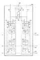
図10の行38は、8個のGOT60、専用素子58、入力62、入力64、出力66、マッチ素子160、複数の行ルーティングライン162、164、166、168、170、172、174、176、178、180、182、184、186、188、190、192(以降、“行ルーティングライン162−192”と集合的に称される)、専用素子ルーティングライン194、複数の接合点196を含んでもよい。
10 includes eight
さらには、図11に示されたSME34、36に結合されるのに加えて、ローカルルーティングマトリクス172は、特定の行38におけるGOT60に対するSME34、36の全ての対に結合されてもよい。したがって、ローカルルーティングマトリクス172は、プログラマブル行内スイッチング素子44と行相互接続導体68、70(以下に記述されるように“行ルーティングライン”とも称される)を含んでもよい。
Further, in addition to being coupled to the
図10に示されたGOT60および専用素子58は、図4に関連して前述されたGOT60と専用素子58に実質的に類似する。従って、各GOT60は、SME34の検出セル86に対してイネーブル信号として動作するための統一型イネーブル入力でありうる入力62を受信する。同様に、各GOT60は、SME36の検出セル86に対するイネーブル信号として動作するための統一型イネーブル入力でもある入力64を受信もする。これらの統一型イネーブル入力62、64は、例えば、データストリーム内のパターンを検索するために、他のSME34、36からの結果と組み合わせて利用されうる、其々のSMEによって実施された解析の其々の結果(例えば、単一のSME34からの解析されたデータストリームにおけるマッチ)を出力するために、SME34、36の検出セル86をアクティブ化してもよい。例えば、統一型イネーブル入力62と統一型イネーブル入力64は、アクティブなSME34、36の各々によって生成された結果がデータストリームの全体のより広い解析の一部として利用されうるように、SME34、36の選択的アクティブ化を可能にする。
The
GOT60のSME34、36によって生成された結果は、出力66上にGOTから選択的に提供されてもよい。一実施形態においては、GOT60の可能性のある出力は、出力を含まないか、第一のSME34の出力(即ち、出力72)と第二のSME36の出力(即ち出力74)を含むか、第一のSME34の出力もしくは第二のSME36の出力(即ち、出力72もしくは出力74)を含む。したがって、GOT60は、GOT60から選択された結果を出力するようにプログラムされてもよい。このプログラミングは、例えば、FSMラチス30の最初のプログラミングステージ間に実施されるロードされた画像に基づいて達成されてもよい。GOT60からの結果は、任意のデータストリーム検索もしくはデータストリーム検索の一部用に行38から生成された選択された結果を出力するように動作しうる、マッチ素子160へと提供されてもよい。
Results generated by the
さらに、行38は、行ルーティングライン162−192(行相互接続導体とも称されうる)を含んでもよい。本実施形態においては、8個のGOT60と専用素子58に選択的に結合可能な16本の行ライン162−192が存在する。しかしながら、より少ないかより多い行ルーティングラインが行38と組み合わせて利用されてもよいことを理解されたい。
Further,
行ルーティングライン162−192の各々は、入力62、64に沿って、一つ以上のGOT60のSME34、36の任意のSMEに対してイネーブル信号を提供するために使用されてもよい。したがって、これらの行ルーティングライン162−192の使用を介して、任意の特定のSME(例えばSME34)に対する任意の特定の検出セル86はアクティブ化されてもよい。これは、SME34、36の統一型イネーブル入力62、64に対して、行ルーティングライン162−192を(例えば、ロードされた画像に従って)選択的に結合することによって達成されてもよい。さらには、SME34、36にイネーブル信号を提供するうえでのさらなる柔軟性を提供するために、行ルーティングライン162−192は、任意のGOT60の二つのSME34、36の間で分割されてもよい。例えば、行ルーティングライン162、164、166、168、170、172、174、176は行38におけるSME34、36のうちの任意のSMEをアクティブ化するために使用されてもよい。例えば、GOT60は、そこに結合された行ルーティングライン(例えば、行ルーティングライン162)へと出力66を伝送してもよい。この信号は、例えば、行38におけるさらなるGOT60へと行ルーティングライン164上でルーティングされうる、ブロック内スイッチへと伝送されてもよい。さらには、行ルーティングライン178、182、186、190は、例えば、ブロック内スイッチ42からの信号を受信することによって、行38におけるSME34をアクティブ化し、行ルーティングライン180、184、188、192は、例えば、ブロック内スイッチ42から受信された信号を介して行38におけるSME36をアクティブ化してもよい。この方法においては、行ルーティングライン162−192の全体の数が減少するが、行38におけるSME34、36のうちの任意のSMEの任意の検出セル86をアクティブ化するための性能および全体の柔軟性を可能とする。
Each of the row routing lines 162-192 may be used to provide an enable signal along any of the
図10に示されるように、各行ルーティングライン162−192は、複数の接合点196を含む。これらの接合点196は、例えば、図3の行内スイッチング素子44を含んでもよい。なぜなら、任意のGOT60を任意の他のGOT60へと選択的に結合するためか、行38(もしくはその点において、別の行および/もしくは別のブロック)内の任意の他の素子(例えば、専用素子58)へと任意のGOT60を選択的に結合するために接合点196が使用されることがあるためである。しかしながら、これらの接続は、利用可能な接合点196によって制限されてもよい。例えば、各行ルーティングライン162、164、166、168、170、172、174、176は、行38におけるSME34、36のうちの任意のSMEをアクティブ化するために使用されてもよい。しかしながら、各行ルーティングライン162、164、166、168、170、172、174、176は、GOT60のうちの其々異なる一つの出力へと選択的に結合可能でもある。例えば、GOT60のうちの任意の一つからの出力は、そこに結合可能な行ルーティングライン162、164、166、168、170、172、174、176のうちのそれぞれ一つの上のGOT60から提供されるだけでもよい。したがって、一実施形態においては、行ルーティングライン162、164、166、168、170、172、174、176は、GOT60の出力66へと結合可能であるため、行ルーティングライン162、164、166、168、170、172、174、176は、ブロック内スイッチ42へと(例えば、駆動)信号を提供してもよい。対照的に、一実施形態においては、行ルーティングライン178、180、182、184、186、188、190、192は、例えば、他の行38もしくはブロック32から受信されることがあるブロック内スイッチ42からの信号を受信して(例えば、それによって駆動されて)もよい。
As shown in FIG. 10, each row routing line 162-192 includes a plurality of junction points 196. These junction points 196 may include, for example, the in-row switching element 44 of FIG. Because any
行ルーティングライン162−192に加えて、行38は、専用素子58に結合された専用素子ルーティングライン194を含んでもよい。行ルーティングライン162、164、166、168、170、172、174、176と類似して、専用ルーティングライン194は、ブロック内スイッチ42へと(例えば、駆動)信号を提供してもよい。一実施形態においては、専用素子ルーティングライン194は、マッチ素子160へと結合可能であってもよい。例えば、専用素子58がカウンタを含む場合、カウンタの出力は、専用ルーティングライン194に沿って提供されてもよい。同様に、専用素子58がブール型セルなどのブール論理素子を含む場合、ブール論理素子の出力は、専用ルーティングライン194に沿って提供されてもよい。これらの専用素子の利用を通して、繰り返し型検索(例えば、10回ある要素を見つける)もしくはカスケード型検索(例えば、要素x、y、zを見つける)は、ブロック内スイッチ42およびマッチ素子160のうちのいずれかまたはその双方へと、専用ルーティングライン194に沿って提供されうる単一の出力へと簡略化されてもよい。
In addition to row routing lines 162-192,
マッチ素子160のより詳細な図が図11に表示される。示されるように、マッチ素子160は、4つのデータ入力198、200、202、204と2つの出力と、6つの制御入力210、212、214、216、218、220を含んでもよい。さらには、マッチ素子は、二つの2:1マルチプレクサ222、224を含んでもよい。2:1マルチプレクサ222、224が示されているが、例えば、ルーティング/出力構成における柔軟性を可能とするため、もしくはシリコンスペースが許すときに、3:1マルチプレクサ、4:1マルチプレクサもしくは他の素子が所望の場合には、2:1マルチプレクサ222、224の位置で使用されてもよいことに留意されたい。
A more detailed view of the
一実施形態においては、マッチ素子160のデータ入力198は、行ルーティングライン176に結合され、データ入力200は行ルーティングライン174に結合され、データ入力202は、専用ルーティングライン194に結合され、データ入力204は行ルーティングライン168に結合される。これらの特定のラインの選択は例示的なためだけのものであって、行38からの出力信号を受信するうえで柔軟性を説明するために選択される。マッチ素子160に接続するものとして、行ルーティングライン168および行ルーティングライン176を選択することによって、GOT60間のパリティを確立することができる。例えば、全てのGOT60のうちの前半(GOT60の0から3)における一つのGOT60によって、データストリームの少なくとも一部で実施される第一の解析の結果は、マッチ素子160へのルーティングライン168上で提供され、全てのGOT60のうちの後半(GOT60の4から7)における別のGOT60によって、データストリームの少なくとも一部で実施される第二の解析の結果は、マッチ素子160へのルーティングライン176上で提供される可能性がある。入力200、204をこの方法で分割することによって、マッチ素子160へと結果を提供するための経路を減少させることを可能とすることができる。さらには、マッチ素子160において、専用ルーティングライン194に沿って専用素子58からの結果を受信することによって、カスケード型検索の結果は、マッチ素子160へと一度に提供されてもよい。最後に、行ルーティングライン174の選択は、行38の全体システムに対して柔軟性を追加する。しかしながら、記述されたように、これらの選択は単に例示的なものにすぎない。
In one embodiment, the
示されるように、マッチ素子160のデータ入力198、200は、2:1マルチプレクサ222に提供され、マッチ素子160のデータ入力202、204は、2:1マルチプレクサ224に提供されてもよい。2:1マルチプレクサ222、224は、例えば、FSMラチス30の最初のプログラミングステージ間に実施されるロードされた画像に基づいてプログラムされうる、制御入力210、212、214、216、218、220から制御信号を各々受信してもよい。一実施形態においては、2:1マルチプレクサ222は、制御入力210から選択信号S0を、制御入力212から選択信号S1を、制御入力214から出力イネーブル信号を受信してもよい。同様に、2:1マルチプレクサ224は、制御入力216から選択信号S0を、制御入力218から選択信号S1を、制御入力220から出力イネーブル信号を受信してもよい。選択信号S0、S1は、其々、例えば出力ブロック54へとデータ検索の結果を伝送するために、どのデータ入力が出力206、208へと提供されるべきかを選択するために使用されてもよい。さらには、選択信号S0、S1を搬送する複数の選択ラインの利用は、インバータなしで各2:1マルチプレクサ222、224を構築することを可能とし、それによって、2:1マルチプレクサ222、224を実装するために必要とされる面積を縮小する。しかしながら、一実施形態においては、単一の選択信号、例えばS0を搬送する単一の選択ラインが使用されてもよい。
As shown, the
さらには、制御入力214からの出力イネーブル信号は、データ入力198、200、202、204上の信号がステーブルであるときにのみ、出力206、208を提供することを可能とするクロック信号もしくは他のイネーブル信号であってもよい。図13は、制御入力210からの選択信号S0、制御入力212からの選択信号S1が2:1マルチプレクサ224の出力208を如何にしてプログラマブルに選択するかの一実施例を説明する真理値表226を示す。
Further, the output enable signal from the
図13に示されるように、マッチ素子160の出力208に対応する真理値表226が示される。真理値表226に表された出力208は、制御入力2220からの出力イネーブル信号が2:1マルチプレクサ224で受信されたことを仮定することに留意されたい。真理値表226に示されたように、制御入力216からの選択信号S0と制御入力218からの選択信号S1の双方がロウ(即ち0)であるとき、2:1マルチプレクサ224の出力208はロウである。例えば、マッチ素子160から提供される行38からの結果はない。制御入力216からの選択信号S0がハイ(即ち1)であって、制御入力218からの選択信号S1がロウであるとき、2:1マルチプレクサ224の出力208は、行ルーティングライン168上の結果である。逆に、制御入力216からの選択信号S0がロウであって、制御入力218からの選択信号S1がハイであるとき、2:1マルチプレクサ224の出力208は、専用ルーティングライン194上の結果である。最後に、制御入力216からの選択信号S0と制御入力218からの選択信号S1の双方がハイになることによる状態は禁じられる。したがって、当該状態は、マッチ素子160のプログラミング中に回避される。この方法においては、マッチ素子160は、出力を選択しないか、第一のデータ入力204からの出力(行ルーティングライン168上の結果)をプログラマブルに選択するか、第二のデータ入力202からの出力(専用ルーティングライン194上の結果)をプログラマブルに選択してもよい。さらには、マッチ素子は、図12に示された特定の実施形態に限定されることなく、他のプログラマブル構成で動作してもよいことに留意されたい。
As shown in FIG. 13, a truth table 226 corresponding to the
本明細書においては、図面で例示する目的のために特定の実施形態が示され、詳細に記述されてきたが、本発明は種々の改変および置換形態が可能であってもよい。しかしながら、本発明は開示された特定の形態に限定されることを意図するものではないことを理解されるべきである。それよりもむしろ、本発明は、以下に添付された請求項によって定義される本発明の趣旨および範囲内にある全ての改変物、均等物、代替物を包含するものである。 Although specific embodiments have been shown and described in detail herein for purposes of illustration in the drawings, the present invention may be susceptible to various modifications and substitutions. However, it should be understood that the invention is not intended to be limited to the particular forms disclosed. On the contrary, the invention is intended to cover all modifications, equivalents, and alternatives falling within the spirit and scope of the invention as defined by the claims appended below.
図4は、行38の一実施例を示す。GOT60は、プログラマブル行内スイッチング素子44によって、行38内の任意の他の素子(例えば、専用素子58)および他のGOT60へと選択的に結合することができる。GOT60は、ブロック内スイッチング素子42で他の行38における他のGOT60へと、または、ブロック間スイッチング素子40によって他のブロック32における他のGOT60へと結合することができる。一実施例においては、GOT60は、第一の入力62、第二の入力64、出力66を有する。図5に関連してさらに示されるように、第一の入力62は、GOT60の第一のSME34へと結合され、第二の入力64は、GOT60の第二のSME34へと結合される。
FIG. 4 shows an example of
一実施例においては、ステートマシン素子34、36は、検出ライン82へとパラレルに結合されたダイナミックランダムアクセスメモリ(DRAM)でしばしば利用されるような複数のメモリセル80を含む。当該メモリセル80のうちの一つは、ハイもしくはロウの値(例えば、1もしくは0)のいずれかに対応するような、データ状態に設定することのできるメモリセルを含む。メモリセル80の出力は、検出ライン82に結合され、メモリセル80の入力は、データストリームライン84上のデータに基づいて信号を受信する。一実施例においては、データストリームライン84上の入力は、メモリセル80のうちの選択された一つへとデコードされる。選択されたメモリセル80は、検出ライン82上の出力としてその格納されたデータ状態を提供する。例えば、入力ブロック52で受信されたデータは、(図示されていない)デコーダへと提供され、デコーダは、データストリームライン84のうちの一つを選択することができる。一実施例においては、デコーダは、256本のデータストリームライン84のうちの対応する1本へと、8ビットASCII文字を変換することができる。
In one embodiment,
解析されるべきデータがバスインターフェイス130で受信され、多数のバッファおよびバッファインターフェイスを通してFSMラチス30へと伝送される。示された実施形態においては、データ経路は、データバッファ132、プロセスバッファ134、インターランク(IR)バスおよびプロセスバッファインターフェイス136を含む。データバッファ132は、解析されるべきデータを受信して一時的に格納するように構成される。一実施形態においては、二つのデータバッファ132(データバッファAおよびデータバッファB)が存在する。データは、二つのデータバッファ132のうちの一つに格納され、データは、FSMラチス30による解析用に他のデータバッファ132から除かれる。示された実施形態においては、データバッファ132は、各々32Kバイトであってもよい。IRバスおよびプロセスバッファインターフェイス136は、プロセスバッファ134へのデータ伝送を容易にしてもよい。IRバスおよびプロセスバッファ134は、データがFSMラチス30によって順番に処理されることを保証する。IRバスおよびプロセスバッファ134は、データが正確な順序で受信されて解析されるように、データの交換、タイミング情報、パッキング命令などを調整してもよい。概して、IRバスおよびプロセスバッファ134は、FSMラチス30の論理ランクを通したパラレルな複数データセットの解析を可能にする。
Data to be analyzed is received at the
さらには、図5に示されたSME34、36に結合されるのに加えて、ローカルルーティングマトリクス172は、特定の行38におけるGOT60に対するSME34、36の全ての対に結合されてもよい。したがって、ローカルルーティングマトリクス172は、プログラマブル行内スイッチング素子44と行相互接続導体68、70(以下に記述されるように“行ルーティングライン”とも称される)を含んでもよい。
Further, in addition to being coupled to the
行ルーティングライン162−192に加えて、行38は、専用素子58に結合された専用素子ルーティングライン194を含んでもよい。行ルーティングライン162、164、166、168、170、172、174、176と類似して、専用素子ルーティングライン194は、ブロック内スイッチ42へと(例えば、駆動)信号を提供してもよい。一実施形態においては、専用素子ルーティングライン194は、マッチ素子160へと結合可能であってもよい。例えば、専用素子58がカウンタを含む場合、カウンタの出力は、専用素子ルーティングライン194に沿って提供されてもよい。同様に、専用素子58がブール型セルなどのブール論理素子を含む場合、ブール論理素子の出力は、専用素子ルーティングライン194に沿って提供されてもよい。これらの専用素子の利用を通して、繰り返し型検索(例えば、10回ある要素を見つける)もしくはカスケード型検索(例えば、要素x、y、zを見つける)は、ブロック内スイッチ42およびマッチ素子160のうちのいずれかまたはその双方へと、専用素子ルーティングライン194に沿って提供されうる単一の出力へと簡略化されてもよい。
In addition to row routing lines 162-192,
一実施形態においては、マッチ素子160のデータ入力198は、行ルーティングライン176に結合され、データ入力200は行ルーティングライン174に結合され、データ入力202は、専用素子ルーティングライン194に結合され、データ入力204は行ルーティングライン168に結合される。これらの特定のラインの選択は例示的なためだけのものであって、行38からの出力信号を受信するうえで柔軟性を説明するために選択される。マッチ素子160に接続するものとして、行ルーティングライン168および行ルーティングライン176を選択することによって、GOT60間のパリティを確立することができる。例えば、全てのGOT60のうちの前半(GOT60の0から3)における一つのGOT60によって、データストリームの少なくとも一部で実施される第一の解析の結果は、マッチ素子160へのルーティングライン168上で提供され、全てのGOT60のうちの後半(GOT60の4から7)における別のGOT60によって、データストリームの少なくとも一部で実施される第二の解析の結果は、マッチ素子160へのルーティングライン176上で提供される可能性がある。入力200、204をこの方法で分割することによって、マッチ素子160へと結果を提供するための経路を減少させることを可能とすることができる。さらには、マッチ素子160において、専用素子ルーティングライン194に沿って専用素子58からの結果を受信することによって、カスケード型検索の結果は、マッチ素子160へと一度に提供されてもよい。最後に、行ルーティングライン174の選択は、行38の全体システムに対して柔軟性を追加する。しかしながら、記述されたように、これらの選択は単に例示的なものにすぎない。
In one embodiment, the
さらには、制御入力214からの出力イネーブル信号は、データ入力198、200、202、204上の信号がステーブルであるときにのみ、出力206、208を提供することを可能とするクロック信号もしくは他のイネーブル信号であってもよい。図12は、制御入力210からの選択信号S0、制御入力212からの選択信号S1が2:1マルチプレクサ224の出力208を如何にしてプログラマブルに選択するかの一実施例を説明する真理値表226を示す。
Further, the output enable signal from the
図12に示されるように、マッチ素子160の出力208に対応する真理値表226が示される。真理値表226に表された出力208は、制御入力2220からの出力イネーブル信号が2:1マルチプレクサ224で受信されたことを仮定することに留意されたい。真理値表226に示されたように、制御入力216からの選択信号S0と制御入力218からの選択信号S1の双方がロウ(即ち0)であるとき、2:1マルチプレクサ224の出力208はロウである。例えば、マッチ素子160から提供される行38からの結果はない。制御入力216からの選択信号S0がハイ(即ち1)であって、制御入力218からの選択信号S1がロウであるとき、2:1マルチプレクサ224の出力208は、行ルーティングライン168上の結果である。逆に、制御入力216からの選択信号S0がロウであって、制御入力218からの選択信号S1がハイであるとき、2:1マルチプレクサ224の出力208は、専用素子ルーティングライン194上の結果である。最後に、制御入力216からの選択信号S0と制御入力218からの選択信号S1の双方がハイになることによる状態は禁じられる。したがって、当該状態は、マッチ素子160のプログラミング中に回避される。この方法においては、マッチ素子160は、出力を選択しないか、第一のデータ入力204からの出力(行ルーティングライン168上の結果)をプログラマブルに選択するか、第二のデータ入力202からの出力(専用素子ルーティングライン194上の結果)をプログラマブルに選択してもよい。さらには、マッチ素子は、図12に示された特定の実施形態に限定されることなく、他のプログラマブル構成で動作してもよいことに留意されたい。
As shown in FIG. 12 , a truth table 226 corresponding to the
Claims (29)
第二の結果を受信するように構成された第二のデータ入力であって、前記第二の結果は、前記ステートマシンの別の素子によって前記データストリームの少なくとも一部上で実施される解析の結果である、第二のデータ入力と、
前記第一の結果もしくは前記第二の結果を選択的に提供するように構成された出力と、
を含むマッチ素子を含む、
ことを特徴とするデバイス。 A first data input configured to receive a first result, wherein the first result is a result of an analysis performed on at least a portion of the data stream by an element of the state machine; The first data entry,
A second data input configured to receive a second result, wherein the second result is an analysis performed on at least a portion of the data stream by another element of the state machine. The resulting second data entry, and
An output configured to selectively provide the first result or the second result;
Including match elements, including
A device characterized by that.
第一の制御信号を受信するように構成された第一の制御入力と、
第二の制御信号を受信するように構成された第二の制御入力と、
を含む、
ことを特徴とする請求項1に記載のデバイス。 The match element is
A first control input configured to receive a first control signal;
A second control input configured to receive a second control signal;
including,
The device according to claim 1.
ことを特徴とする請求項2に記載のデバイス。 The output configured to selectively provide the first result or the second result is based on the first and second control signals, the first result or the second result. Including the output configured to selectively provide
The device according to claim 2.
ことを特徴とする請求項3に記載のデバイス。 The match element includes a third control input configured to receive an output enable signal;
The device according to claim 3.
ことを特徴とする請求項4に記載のデバイス。 The outputs configured to provide the first result or the second result based on the first and second control signals are the first and second control signals and the output enable signal. Including the match element configured to provide the first result or the second result based on:
The device of claim 4.
ことを特徴とする請求項4に記載のデバイス。 The match element is a 2: 1 multiplexer coupled to the first data input, the second data input, the first control input, the second control input, the third control input, and the output. including,
The device of claim 4.
ことを特徴とする請求項1に記載のデバイス。 The output configured to selectively provide the first result or the second result does not provide an output, or selectively provides the first result or the second result. Including the output configured in
The device according to claim 1.
第三の結果を受信するように構成された第三のデータ入力であって、前記第三の結果は、前記ステートマシンの第三の素子によって前記データストリームの少なくとも一部上で実施された解析の結果である、第三のデータ入力と、
第四の結果を受信するように構成された第四のデータ入力であって、前記第四の結果は、前記ステートマシンの専用素子によって検出された複数の結果の組み合わせを含む、第四のデータ入力と、
前記第三の結果もしくは前記第四の結果を選択的に提供するように構成された第二の出力と、
を含む、
ことを特徴とする請求項2に記載のデバイス。 The match element is
A third data input configured to receive a third result, wherein the third result is an analysis performed on at least a portion of the data stream by a third element of the state machine; A third data entry that is the result of
A fourth data input configured to receive a fourth result, wherein the fourth result comprises a combination of a plurality of results detected by a dedicated element of the state machine; Input,
A second output configured to selectively provide the third result or the fourth result;
including,
The device according to claim 2.
第三の制御信号を受信するように構成された第三の制御入力と、
第四の制御信号を受信するように構成された第四の制御入力と、
を含む、
ことを特徴とする請求項8に記載のデバイス。 The match element is
A third control input configured to receive a third control signal;
A fourth control input configured to receive a fourth control signal;
including,
The device according to claim 8.
ことを特徴とする請求項9に記載のデバイス。 The second output configured to selectively provide the third result or the fourth result is based on the third and fourth control signals, the third result or the fourth result. Including the second output configured to selectively provide four results;
The device according to claim 9.
ことを特徴とする請求項10に記載のデバイス。 The match element includes a fifth control input configured to receive an output enable signal;
The device according to claim 10.
ことを特徴とする請求項11に記載のデバイス。 Based on the third and fourth control signals, the match element configured to provide the third result or the fourth result includes the third and fourth control signals and the output enable. Including the match element configured to provide the third result or the fourth result based on a signal;
The device of claim 11.
ことを特徴とする請求項11に記載のデバイス。 The match element is coupled to the third data input, the fourth data input, the third control input, the fourth control input, the fifth control input, and the second output. : 1 including multiplexer
The device of claim 11.
前記データストリームの少なくとも一部上で実施される解析の第二の結果を提供するように構成された第二の素子と、
マッチ素子であって、
前記第一の結果を受信するように構成された第一の入力と、
前記第二の結果を受信するように構成された第二の入力と、
前記第一の結果もしくは前記第二の結果を選択的に提供するように構成された出力と、
を含むマッチ素子と、
を各々含む複数の行、
を各々含む複数のブロック、
を含むステートマシン、
を含む、
ことを特徴とするデバイス。 A first element configured to provide a first result of an analysis performed on at least a portion of the data stream;
A second element configured to provide a second result of an analysis performed on at least a portion of the data stream;
A match element,
A first input configured to receive the first result;
A second input configured to receive the second result;
An output configured to selectively provide the first result or the second result;
A match element including:
A plurality of lines, each containing
A plurality of blocks each including
Including state machine,
including,
A device characterized by that.
ことを特徴とする請求項1に記載のデバイス。 The output configured to selectively provide the first result or the second result does not provide an output, or selectively provides the first result or the second result. Including the output configured in
The device according to claim 1.
ことを特徴とする請求項14に記載のデバイス。 Each of the plurality of rows includes a plurality of row routing lines configured to be selectively coupled to the first element and the second element;
The device according to claim 14.
ことを特徴とする請求項16に記載のデバイス。 Each of the plurality of rows includes a plurality of junctions configured to selectively couple a plurality of selected row routing lines to each of the first element and the second element;
The device of claim 16.
ことを特徴とする請求項17に記載のデバイス。 At least one of the plurality of junctions is configured to selectively couple at least one of the row routing lines to the match element;
The device of claim 17.
ことを特徴とする請求項14に記載のデバイス。 Each of the plurality of rows includes a dedicated element configured to provide a dedicated result, the dedicated result based on a combination of a plurality of results from an analysis performed on at least a portion of the data stream. ,
The device according to claim 14.
ことを特徴とする請求項19に記載のデバイス。 Each of the plurality of rows includes a third element configured to provide a third result of an analysis performed on at least a portion of the data stream;
The device of claim 19.
前記第三の結果を受信するように構成された第三の入力と、
前記専用結果を受信するように構成された第四の入力と、
前記第三の結果もしくは前記専用結果を選択的に提供するように構成された第二の出力と、
をさらに含む、
ことを特徴とする請求項20に記載のデバイス。 The match element is
A third input configured to receive the third result;
A fourth input configured to receive the dedicated result;
A second output configured to selectively provide the third result or the dedicated result;
Further including
The device of claim 20.
前記ステートマシンの第二の素子によって、前記データストリームの少なくとも一部上で実施された解析の第二の結果を、前記マッチ素子の第二のデータ入力で受信することと、
前記第一の結果もしくは前記第二の結果を前記マッチ素子から選択的に出力することと、
を含む、
ことを特徴とする方法。 Receiving a first result of an analysis performed on at least a portion of the data stream by a first element of the state machine at a first data input of the match element;
Receiving a second result of an analysis performed on at least a portion of the data stream by a second element of the state machine at a second data input of the match element;
Selectively outputting the first result or the second result from the match element;
including,
A method characterized by that.
前記マッチ素子で第二の制御信号を受信することと、
を含む、
ことを特徴とする請求項22に記載の方法。 Receiving a first control signal at the match element;
Receiving a second control signal at the match element;
including,
23. The method of claim 22, wherein:
ことを特徴とする請求項23に記載の方法。 The selective output of the first result or the second result from the match element does not output an output from the match element based on the first and second control signals. Selectively outputting the result or the second result from the match element,
24. The method of claim 23.
ことを特徴とする請求項24に記載の方法。 Further receiving an output enable signal at the match element, and based on the first and second control signals, output no output from the match element, the first result or the second result. The selective output from the match element means that no output is output from the match element based on the first and second control signals and the output enable signal, the first result or the second Selectively outputting the result of the match from the match element,
25. The method of claim 24.
前記マッチ素子で第四の結果を受信することであって、前記第四の結果は前記ステートマシンの専用素子によって検出された複数の結果の組み合わせを含む、ことと、
前記第三の結果もしくは前記第四の結果を、前記マッチ素子から選択的に出力することと、
を含む、
ことを特徴とする請求項26に記載の方法。 Receiving at the match element a third result of an analysis performed on at least a portion of the data stream by a third element of the state machine;
Receiving a fourth result at the match element, wherein the fourth result comprises a combination of a plurality of results detected by a dedicated element of the state machine;
Selectively outputting the third result or the fourth result from the match element;
including,
27. A method according to claim 26.
前記マッチ素子で第四の制御信号を受信することと、
を含み、
前記第三の結果もしくは前記第四の結果を前記マッチ素子から選択的に出力することは、前記第三および第四の制御信号に基づいて、前記第三の結果もしくは前記第四の結果を前記マッチ素子から選択的に出力することを含む、
ことを特徴とする請求項27に記載の方法。 Receiving a third control signal at the match element;
Receiving a fourth control signal at the match element;
Including
The selective output of the third result or the fourth result from the match element means that the third result or the fourth result is based on the third and fourth control signals. Including selectively outputting from a match element,
28. The method of claim 27.
ことを特徴とする請求項28に記載の方法。 Receiving the output enable signal at the match element, and selectively outputting the third result or the fourth result from the match element based on the third and fourth control signals. Including selectively outputting the third result or the fourth result from the match element based on the third and fourth control signals and the output enable signal.
29. The method of claim 28, wherein:
ことを特徴とするデバイス。 Including a match element including a plurality of data inputs configured to receive a plurality of instructions in which a plurality of results of analysis of the data stream are detected by one or more state machine elements;
A device characterized by that.
Applications Claiming Priority (3)
| Application Number | Priority Date | Filing Date | Title |
|---|---|---|---|
| US13/327,591 US9443156B2 (en) | 2011-12-15 | 2011-12-15 | Methods and systems for data analysis in a state machine |
| US13/327,591 | 2011-12-15 | ||
| PCT/US2012/067999 WO2013090094A1 (en) | 2011-12-15 | 2012-12-05 | Methods and systems for data analysis in a state machine |
Publications (2)
| Publication Number | Publication Date |
|---|---|
| JP2015507255A true JP2015507255A (en) | 2015-03-05 |
| JP6082753B2 JP6082753B2 (en) | 2017-02-15 |
Family
ID=47561803
Family Applications (1)
| Application Number | Title | Priority Date | Filing Date |
|---|---|---|---|
| JP2014547290A Active JP6082753B2 (en) | 2011-12-15 | 2012-12-05 | Method and system for data analysis in a state machine |
Country Status (7)
| Country | Link |
|---|---|
| US (4) | US9443156B2 (en) |
| EP (1) | EP2791781B1 (en) |
| JP (1) | JP6082753B2 (en) |
| KR (1) | KR101996961B1 (en) |
| CN (2) | CN107609644B (en) |
| TW (1) | TWI515669B (en) |
| WO (1) | WO2013090094A1 (en) |
Families Citing this family (38)
| Publication number | Priority date | Publication date | Assignee | Title |
|---|---|---|---|---|
| US20100138575A1 (en) | 2008-12-01 | 2010-06-03 | Micron Technology, Inc. | Devices, systems, and methods to synchronize simultaneous dma parallel processing of a single data stream by multiple devices |
| US20100174887A1 (en) | 2009-01-07 | 2010-07-08 | Micron Technology Inc. | Buses for Pattern-Recognition Processors |
| US8489534B2 (en) * | 2009-12-15 | 2013-07-16 | Paul D. Dlugosch | Adaptive content inspection |
| US9323994B2 (en) | 2009-12-15 | 2016-04-26 | Micron Technology, Inc. | Multi-level hierarchical routing matrices for pattern-recognition processors |
| US9443156B2 (en) | 2011-12-15 | 2016-09-13 | Micron Technology, Inc. | Methods and systems for data analysis in a state machine |
| US8593175B2 (en) | 2011-12-15 | 2013-11-26 | Micron Technology, Inc. | Boolean logic in a state machine lattice |
| US8680888B2 (en) | 2011-12-15 | 2014-03-25 | Micron Technologies, Inc. | Methods and systems for routing in a state machine |
| US8782624B2 (en) | 2011-12-15 | 2014-07-15 | Micron Technology, Inc. | Methods and systems for detection in a state machine |
| US8648621B2 (en) | 2011-12-15 | 2014-02-11 | Micron Technology, Inc. | Counter operation in a state machine lattice |
| US20130275709A1 (en) | 2012-04-12 | 2013-10-17 | Micron Technology, Inc. | Methods for reading data from a storage buffer including delaying activation of a column select |
| US9389841B2 (en) * | 2012-07-18 | 2016-07-12 | Micron Technology, Inc. | Methods and systems for using state vector data in a state machine engine |
| US9524248B2 (en) | 2012-07-18 | 2016-12-20 | Micron Technology, Inc. | Memory management for a hierarchical memory system |
| US9235798B2 (en) | 2012-07-18 | 2016-01-12 | Micron Technology, Inc. | Methods and systems for handling data received by a state machine engine |
| US9075428B2 (en) | 2012-08-31 | 2015-07-07 | Micron Technology, Inc. | Results generation for state machine engines |
| US9063532B2 (en) * | 2012-08-31 | 2015-06-23 | Micron Technology, Inc. | Instruction insertion in state machine engines |
| US9501131B2 (en) | 2012-08-31 | 2016-11-22 | Micron Technology, Inc. | Methods and systems for power management in a pattern recognition processing system |
| US9703574B2 (en) | 2013-03-15 | 2017-07-11 | Micron Technology, Inc. | Overflow detection and correction in state machine engines |
| US9448965B2 (en) * | 2013-03-15 | 2016-09-20 | Micron Technology, Inc. | Receiving data streams in parallel and providing a first portion of data to a first state machine engine and a second portion to a second state machine |
| FR3011659B1 (en) * | 2013-10-04 | 2015-10-16 | Commissariat Energie Atomique | ELECTRONIC CIRCUIT, PARTICULARLY ABLE TO IMPLEMENTATION OF A NETWORK OF NEURONS, AND NEURONAL SYSTEM |
| US10430210B2 (en) | 2014-12-30 | 2019-10-01 | Micron Technology, Inc. | Systems and devices for accessing a state machine |
| WO2016109571A1 (en) * | 2014-12-30 | 2016-07-07 | Micron Technology, Inc | Devices for time division multiplexing of state machine engine signals |
| US11366675B2 (en) | 2014-12-30 | 2022-06-21 | Micron Technology, Inc. | Systems and devices for accessing a state machine |
| CN104516820B (en) * | 2015-01-16 | 2017-10-27 | 浪潮(北京)电子信息产业有限公司 | A kind of one-hot encoding detection method and one-hot encoding detector |
| US10691964B2 (en) | 2015-10-06 | 2020-06-23 | Micron Technology, Inc. | Methods and systems for event reporting |
| US10977309B2 (en) | 2015-10-06 | 2021-04-13 | Micron Technology, Inc. | Methods and systems for creating networks |
| US10846103B2 (en) | 2015-10-06 | 2020-11-24 | Micron Technology, Inc. | Methods and systems for representing processing resources |
| US10146555B2 (en) | 2016-07-21 | 2018-12-04 | Micron Technology, Inc. | Adaptive routing to avoid non-repairable memory and logic defects on automata processor |
| US10019311B2 (en) | 2016-09-29 | 2018-07-10 | Micron Technology, Inc. | Validation of a symbol response memory |
| US10268602B2 (en) | 2016-09-29 | 2019-04-23 | Micron Technology, Inc. | System and method for individual addressing |
| US10929764B2 (en) | 2016-10-20 | 2021-02-23 | Micron Technology, Inc. | Boolean satisfiability |
| US10592450B2 (en) | 2016-10-20 | 2020-03-17 | Micron Technology, Inc. | Custom compute cores in integrated circuit devices |
| US10481881B2 (en) * | 2017-06-22 | 2019-11-19 | Archeo Futurus, Inc. | Mapping a computer code to wires and gates |
| US9996328B1 (en) * | 2017-06-22 | 2018-06-12 | Archeo Futurus, Inc. | Compiling and optimizing a computer code by minimizing a number of states in a finite machine corresponding to the computer code |
| US10514914B2 (en) * | 2017-08-29 | 2019-12-24 | Gsi Technology Inc. | Method for min-max computation in associative memory |
| US10826801B1 (en) | 2019-07-31 | 2020-11-03 | Bank Of America Corporation | Multi-level data channel and inspection architectures |
| US11115310B2 (en) | 2019-08-06 | 2021-09-07 | Bank Of America Corporation | Multi-level data channel and inspection architectures having data pipes in parallel connections |
| US11470046B2 (en) | 2019-08-26 | 2022-10-11 | Bank Of America Corporation | Multi-level data channel and inspection architecture including security-level-based filters for diverting network traffic |
| CN113379047B (en) * | 2021-05-25 | 2024-04-05 | 北京微芯智通科技合伙企业(有限合伙) | System and method for realizing convolutional neural network processing |
Citations (2)
| Publication number | Priority date | Publication date | Assignee | Title |
|---|---|---|---|---|
| JPH04116475A (en) * | 1990-09-06 | 1992-04-16 | Hitachi Ltd | Semiconductor integration circuit |
| US20110145544A1 (en) * | 2009-12-15 | 2011-06-16 | Micron Technology, Inc. | Multi-level hierarchical routing matrices for pattern-recognition processors |
Family Cites Families (52)
| Publication number | Priority date | Publication date | Assignee | Title |
|---|---|---|---|---|
| US5357512A (en) * | 1992-12-30 | 1994-10-18 | Intel Corporation | Conditional carry scheduler for round robin scheduling |
| US5790531A (en) * | 1994-12-23 | 1998-08-04 | Applied Digital Access, Inc. | Method and apparatus for determining the origin of a remote alarm indication signal |
| US6097212A (en) * | 1997-10-09 | 2000-08-01 | Lattice Semiconductor Corporation | Variable grain architecture for FPGA integrated circuits |
| US20020069379A1 (en) * | 2000-12-05 | 2002-06-06 | Cirrus Logic, Inc. | Servo data detection with improved phase shift tolerance |
| CN1582533A (en) * | 2001-10-29 | 2005-02-16 | 捷豹逻辑股份有限公司 | Programmable interface for field programmable gate array cores |
| US7333580B2 (en) * | 2002-01-28 | 2008-02-19 | Broadcom Corporation | Pipelined parallel processing of feedback loops in a digital circuit |
| US6880146B2 (en) * | 2003-01-31 | 2005-04-12 | Hewlett-Packard Development Company, L.P. | Molecular-wire-based restorative multiplexer, and method for constructing a multiplexer based on a configurable, molecular-junction-nanowire crossbar |
| US7305047B1 (en) * | 2003-03-12 | 2007-12-04 | Lattice Semiconductor Corporation | Automatic lane assignment for a receiver |
| US7366352B2 (en) | 2003-03-20 | 2008-04-29 | International Business Machines Corporation | Method and apparatus for performing fast closest match in pattern recognition |
| DE102004045527B4 (en) * | 2003-10-08 | 2009-12-03 | Siemens Ag | Configurable logic circuitry |
| US7487542B2 (en) * | 2004-01-14 | 2009-02-03 | International Business Machines Corporation | Intrusion detection using a network processor and a parallel pattern detection engine |
| US7176717B2 (en) * | 2005-01-14 | 2007-02-13 | Velogix, Inc. | Programmable logic and routing blocks with dedicated lines |
| US7358761B1 (en) * | 2005-01-21 | 2008-04-15 | Csitch Corporation | Versatile multiplexer-structures in programmable logic using serial chaining and novel selection schemes |
| US7392229B2 (en) * | 2005-02-12 | 2008-06-24 | Curtis L. Harris | General purpose set theoretic processor |
| US7804719B1 (en) * | 2005-06-14 | 2010-09-28 | Xilinx, Inc. | Programmable logic block having reduced output delay during RAM write processes when programmed to function in RAM mode |
| US7276934B1 (en) * | 2005-06-14 | 2007-10-02 | Xilinx, Inc. | Integrated circuit with programmable routing structure including diagonal interconnect lines |
| US8065249B1 (en) * | 2006-10-13 | 2011-11-22 | Harris Curtis L | GPSTP with enhanced aggregation functionality |
| US7774286B1 (en) | 2006-10-24 | 2010-08-10 | Harris Curtis L | GPSTP with multiple thread functionality |
| US7735045B1 (en) * | 2008-03-12 | 2010-06-08 | Xilinx, Inc. | Method and apparatus for mapping flip-flop logic onto shift register logic |
| US8015530B1 (en) * | 2008-08-05 | 2011-09-06 | Xilinx, Inc. | Method of enabling the generation of reset signals in an integrated circuit |
| US8209521B2 (en) | 2008-10-18 | 2012-06-26 | Micron Technology, Inc. | Methods of indirect register access including automatic modification of a directly accessible address register |
| US8938590B2 (en) | 2008-10-18 | 2015-01-20 | Micron Technology, Inc. | Indirect register access method and system |
| US9639493B2 (en) | 2008-11-05 | 2017-05-02 | Micron Technology, Inc. | Pattern-recognition processor with results buffer |
| US7917684B2 (en) | 2008-11-05 | 2011-03-29 | Micron Technology, Inc. | Bus translator |
| US7970964B2 (en) | 2008-11-05 | 2011-06-28 | Micron Technology, Inc. | Methods and systems to accomplish variable width data input |
| US20100118425A1 (en) | 2008-11-11 | 2010-05-13 | Menachem Rafaelof | Disturbance rejection in a servo control loop using pressure-based disc mode sensor |
| US9348784B2 (en) | 2008-12-01 | 2016-05-24 | Micron Technology, Inc. | Systems and methods for managing endian mode of a device |
| US20100138575A1 (en) | 2008-12-01 | 2010-06-03 | Micron Technology, Inc. | Devices, systems, and methods to synchronize simultaneous dma parallel processing of a single data stream by multiple devices |
| US10007486B2 (en) | 2008-12-01 | 2018-06-26 | Micron Technology, Inc. | Systems and methods to enable identification of different data sets |
| US9164945B2 (en) | 2008-12-01 | 2015-10-20 | Micron Technology, Inc. | Devices, systems, and methods to synchronize parallel processing of a single data stream |
| US8140780B2 (en) | 2008-12-31 | 2012-03-20 | Micron Technology, Inc. | Systems, methods, and devices for configuring a device |
| US8214672B2 (en) | 2009-01-07 | 2012-07-03 | Micron Technology, Inc. | Method and systems for power consumption management of a pattern-recognition processor |
| US20100174887A1 (en) | 2009-01-07 | 2010-07-08 | Micron Technology Inc. | Buses for Pattern-Recognition Processors |
| US8281395B2 (en) * | 2009-01-07 | 2012-10-02 | Micron Technology, Inc. | Pattern-recognition processor with matching-data reporting module |
| US8843523B2 (en) | 2009-01-12 | 2014-09-23 | Micron Technology, Inc. | Devices, systems, and methods for communicating pattern matching results of a parallel pattern search engine |
| US8146040B1 (en) * | 2009-06-11 | 2012-03-27 | Xilinx, Inc. | Method of evaluating an architecture for an integrated circuit device |
| US9836555B2 (en) | 2009-06-26 | 2017-12-05 | Micron Technology, Inc. | Methods and devices for saving and/or restoring a state of a pattern-recognition processor |
| US8489534B2 (en) | 2009-12-15 | 2013-07-16 | Paul D. Dlugosch | Adaptive content inspection |
| US9501705B2 (en) | 2009-12-15 | 2016-11-22 | Micron Technology, Inc. | Methods and apparatuses for reducing power consumption in a pattern recognition processor |
| US8601013B2 (en) * | 2010-06-10 | 2013-12-03 | Micron Technology, Inc. | Analyzing data using a hierarchical structure |
| US8766666B2 (en) * | 2010-06-10 | 2014-07-01 | Micron Technology, Inc. | Programmable device, hierarchical parallel machines, and methods for providing state information |
| US8294490B1 (en) * | 2010-10-01 | 2012-10-23 | Xilinx, Inc. | Integrated circuit and method of asynchronously routing data in an integrated circuit |
| JP5848778B2 (en) | 2011-01-25 | 2016-01-27 | マイクロン テクノロジー, インク. | Use of dedicated elements to implement FSM |
| WO2012103151A2 (en) * | 2011-01-25 | 2012-08-02 | Micron Technology, Inc. | State grouping for element utilization |
| JP5763783B2 (en) * | 2011-01-25 | 2015-08-12 | マイクロン テクノロジー, インク. | Method and apparatus for compiling regular expressions |
| US8726256B2 (en) | 2011-01-25 | 2014-05-13 | Micron Technology, Inc. | Unrolling quantifications to control in-degree and/or out-degree of automaton |
| US8593175B2 (en) | 2011-12-15 | 2013-11-26 | Micron Technology, Inc. | Boolean logic in a state machine lattice |
| US9443156B2 (en) | 2011-12-15 | 2016-09-13 | Micron Technology, Inc. | Methods and systems for data analysis in a state machine |
| US8680888B2 (en) * | 2011-12-15 | 2014-03-25 | Micron Technologies, Inc. | Methods and systems for routing in a state machine |
| US8782624B2 (en) | 2011-12-15 | 2014-07-15 | Micron Technology, Inc. | Methods and systems for detection in a state machine |
| US8648621B2 (en) | 2011-12-15 | 2014-02-11 | Micron Technology, Inc. | Counter operation in a state machine lattice |
| US8536896B1 (en) * | 2012-05-31 | 2013-09-17 | Xilinx, Inc. | Programmable interconnect element and method of implementing a programmable interconnect element |
-
2011
- 2011-12-15 US US13/327,591 patent/US9443156B2/en active Active
-
2012
- 2012-12-05 JP JP2014547290A patent/JP6082753B2/en active Active
- 2012-12-05 KR KR1020147018494A patent/KR101996961B1/en active IP Right Grant
- 2012-12-05 EP EP12816168.4A patent/EP2791781B1/en active Active
- 2012-12-05 WO PCT/US2012/067999 patent/WO2013090094A1/en active Application Filing
- 2012-12-05 CN CN201710652791.XA patent/CN107609644B/en active Active
- 2012-12-05 CN CN201280062293.5A patent/CN103999035B/en active Active
- 2012-12-14 TW TW101147678A patent/TWI515669B/en active
-
2016
- 2016-09-12 US US15/262,958 patent/US9870530B2/en active Active
-
2018
- 2018-01-15 US US15/871,660 patent/US10733508B2/en active Active
-
2020
- 2020-06-30 US US16/917,221 patent/US11977977B2/en active Active
Patent Citations (2)
| Publication number | Priority date | Publication date | Assignee | Title |
|---|---|---|---|---|
| JPH04116475A (en) * | 1990-09-06 | 1992-04-16 | Hitachi Ltd | Semiconductor integration circuit |
| US20110145544A1 (en) * | 2009-12-15 | 2011-06-16 | Micron Technology, Inc. | Multi-level hierarchical routing matrices for pattern-recognition processors |
Also Published As
| Publication number | Publication date |
|---|---|
| TW201333838A (en) | 2013-08-16 |
| US9870530B2 (en) | 2018-01-16 |
| WO2013090094A1 (en) | 2013-06-20 |
| KR20140104991A (en) | 2014-08-29 |
| KR101996961B1 (en) | 2019-07-05 |
| US20200334533A1 (en) | 2020-10-22 |
| CN107609644B (en) | 2021-03-16 |
| US11977977B2 (en) | 2024-05-07 |
| TWI515669B (en) | 2016-01-01 |
| EP2791781A1 (en) | 2014-10-22 |
| US20180137416A1 (en) | 2018-05-17 |
| US10733508B2 (en) | 2020-08-04 |
| JP6082753B2 (en) | 2017-02-15 |
| US20160379114A1 (en) | 2016-12-29 |
| EP2791781B1 (en) | 2021-07-14 |
| CN107609644A (en) | 2018-01-19 |
| US20130159239A1 (en) | 2013-06-20 |
| US9443156B2 (en) | 2016-09-13 |
| CN103999035B (en) | 2017-09-22 |
| CN103999035A (en) | 2014-08-20 |
Similar Documents
| Publication | Publication Date | Title |
|---|---|---|
| US11977977B2 (en) | Methods and systems for data analysis in a state machine | |
| JP6126127B2 (en) | Method and system for routing in a state machine | |
| US9817678B2 (en) | Methods and systems for detection in a state machine | |
| JP6154824B2 (en) | Boolean logic in state machine lattices | |
| JP6207605B2 (en) | Method and device for programming a state machine engine | |
| JP6109186B2 (en) | Counter operation in a state machine grid | |
| JP6041987B2 (en) | Method and system for using state vector data in a state machine engine |
Legal Events
| Date | Code | Title | Description |
|---|---|---|---|
| A621 | Written request for application examination |
Free format text: JAPANESE INTERMEDIATE CODE: A621 Effective date: 20150903 |
|
| A977 | Report on retrieval |
Free format text: JAPANESE INTERMEDIATE CODE: A971007 Effective date: 20160727 |
|
| A131 | Notification of reasons for refusal |
Free format text: JAPANESE INTERMEDIATE CODE: A131 Effective date: 20160802 |
|
| A521 | Request for written amendment filed |
Free format text: JAPANESE INTERMEDIATE CODE: A523 Effective date: 20161006 |
|
| A131 | Notification of reasons for refusal |
Free format text: JAPANESE INTERMEDIATE CODE: A131 Effective date: 20161101 |
|
| A521 | Request for written amendment filed |
Free format text: JAPANESE INTERMEDIATE CODE: A523 Effective date: 20161214 |
|
| TRDD | Decision of grant or rejection written | ||
| A01 | Written decision to grant a patent or to grant a registration (utility model) |
Free format text: JAPANESE INTERMEDIATE CODE: A01 Effective date: 20170117 |
|
| A61 | First payment of annual fees (during grant procedure) |
Free format text: JAPANESE INTERMEDIATE CODE: A61 Effective date: 20170123 |
|
| R150 | Certificate of patent or registration of utility model |
Ref document number: 6082753 Country of ref document: JP Free format text: JAPANESE INTERMEDIATE CODE: R150 |
|
| R250 | Receipt of annual fees |
Free format text: JAPANESE INTERMEDIATE CODE: R250 |
|
| R250 | Receipt of annual fees |
Free format text: JAPANESE INTERMEDIATE CODE: R250 |
|
| R250 | Receipt of annual fees |
Free format text: JAPANESE INTERMEDIATE CODE: R250 |
|
| R250 | Receipt of annual fees |
Free format text: JAPANESE INTERMEDIATE CODE: R250 |
|
| R250 | Receipt of annual fees |
Free format text: JAPANESE INTERMEDIATE CODE: R250 |