JP2014500977A - Optical interconnect fabric implemented using star couplers - Google Patents
Optical interconnect fabric implemented using star couplers Download PDFInfo
- Publication number
- JP2014500977A JP2014500977A JP2013536579A JP2013536579A JP2014500977A JP 2014500977 A JP2014500977 A JP 2014500977A JP 2013536579 A JP2013536579 A JP 2013536579A JP 2013536579 A JP2013536579 A JP 2013536579A JP 2014500977 A JP2014500977 A JP 2014500977A
- Authority
- JP
- Japan
- Prior art keywords
- optical
- output
- star coupler
- input
- optical fiber
- Prior art date
- Legal status (The legal status is an assumption and is not a legal conclusion. Google has not performed a legal analysis and makes no representation as to the accuracy of the status listed.)
- Pending
Links
Images


Classifications
-
- G—PHYSICS
- G02—OPTICS
- G02B—OPTICAL ELEMENTS, SYSTEMS OR APPARATUS
- G02B6/00—Light guides; Structural details of arrangements comprising light guides and other optical elements, e.g. couplings
- G02B6/24—Coupling light guides
- G02B6/26—Optical coupling means
- G02B6/28—Optical coupling means having data bus means, i.e. plural waveguides interconnected and providing an inherently bidirectional system by mixing and splitting signals
- G02B6/2804—Optical coupling means having data bus means, i.e. plural waveguides interconnected and providing an inherently bidirectional system by mixing and splitting signals forming multipart couplers without wavelength selective elements, e.g. "T" couplers, star couplers
- G02B6/2817—Optical coupling means having data bus means, i.e. plural waveguides interconnected and providing an inherently bidirectional system by mixing and splitting signals forming multipart couplers without wavelength selective elements, e.g. "T" couplers, star couplers using reflective elements to split or combine optical signals
-
- G—PHYSICS
- G02—OPTICS
- G02B—OPTICAL ELEMENTS, SYSTEMS OR APPARATUS
- G02B6/00—Light guides; Structural details of arrangements comprising light guides and other optical elements, e.g. couplings
- G02B6/24—Coupling light guides
- G02B6/26—Optical coupling means
- G02B6/28—Optical coupling means having data bus means, i.e. plural waveguides interconnected and providing an inherently bidirectional system by mixing and splitting signals
- G02B6/293—Optical coupling means having data bus means, i.e. plural waveguides interconnected and providing an inherently bidirectional system by mixing and splitting signals with wavelength selective means
- G02B6/29346—Optical coupling means having data bus means, i.e. plural waveguides interconnected and providing an inherently bidirectional system by mixing and splitting signals with wavelength selective means operating by wave or beam interference
- G02B6/29361—Interference filters, e.g. multilayer coatings, thin film filters, dichroic splitters or mirrors based on multilayers, WDM filters
- G02B6/29362—Serial cascade of filters or filtering operations, e.g. for a large number of channels
- G02B6/29365—Serial cascade of filters or filtering operations, e.g. for a large number of channels in a multireflection configuration, i.e. beam following a zigzag path between filters or filtering operations
- G02B6/29367—Zigzag path within a transparent optical block, e.g. filter deposited on an etalon, glass plate, wedge acting as a stable spacer
-
- G—PHYSICS
- G02—OPTICS
- G02B—OPTICAL ELEMENTS, SYSTEMS OR APPARATUS
- G02B6/00—Light guides; Structural details of arrangements comprising light guides and other optical elements, e.g. couplings
- G02B6/24—Coupling light guides
- G02B6/36—Mechanical coupling means
- G02B6/38—Mechanical coupling means having fibre to fibre mating means
- G02B6/3807—Dismountable connectors, i.e. comprising plugs
-
- H—ELECTRICITY
- H04—ELECTRIC COMMUNICATION TECHNIQUE
- H04J—MULTIPLEX COMMUNICATION
- H04J14/00—Optical multiplex systems
- H04J14/02—Wavelength-division multiplex systems
- H04J14/0278—WDM optical network architectures
- H04J14/0282—WDM tree architectures
Abstract
本開示は、コンピュータシステムにわたって光信号を配信するための拡張性のある光相互接続ファブリックを対象とする。一態様では、光相互接続ファブリックが、スターカプラ504、802及び複数の出力光ファイバ508、812を備える。各出力光ファイバは、第1の端がスターカプラに接続され、第2の端が複数のノードのうちの1つのノードに接続されている。このファブリックは、第1の端がスターカプラ504、802に接続され、第2の端が複数のノードのうちの1つのノードに接続されている入力光ファイバ505、804〜806も備える。スターカプラは、入力光ファイバを介して少なくとも1つの光信号を受信し、各光信号をほぼ同じ光パワーを有する複数の光信号に分離し、各光信号を出力光ファイバのうちの1つに出力する。
【選択図】図1AThe present disclosure is directed to a scalable optical interconnect fabric for distributing optical signals across a computer system. In one aspect, the optical interconnect fabric comprises star couplers 504, 802 and a plurality of output optical fibers 508, 812. Each output optical fiber has a first end connected to the star coupler and a second end connected to one of the plurality of nodes. The fabric also includes input optical fibers 505, 804-806 having a first end connected to the star couplers 504, 802 and a second end connected to one of the nodes. The star coupler receives at least one optical signal via the input optical fiber, separates each optical signal into a plurality of optical signals having substantially the same optical power, and each optical signal is output to one of the output optical fibers. Output.
[Selection] Figure 1A
Description
本開示は、コンピュータバスに関し、特に光バスに関する。 The present disclosure relates to computer buses, and more particularly to optical buses.
ブレードシステム等の一般的な高性能ラックマウントコンピュータシステムは、電子相互接続ファブリックによって電子通信する複数のプロセッサ基板及びメモリ基板を備える。理想的な相互接続ファブリックは、増加の一途をたどるように見える計算需要を満たすのに十分なメモリ及び処理速度を提供するために、プロセッサ及びメモリが独立して拡張することを可能にする。しかしながら、電子相互接続ファブリックは、拡張による複数の不利な点を有する。電子相互接続ファブリックは、セットアップするのに大きな労働力を要する可能性があり、電子信号を従来の電子相互接続によって送信することは、大量の電力を消費する。加えて、電子相互接続の帯域幅を拡張することはますます困難になってきており、電子相互接続ファブリックによって電子信号を送信するのに必要な相対的な時間の量が、より小さくより高速なプロセッサによって提供される高速性能の利点を完全に利用するのに長くなり過ぎてきている。 A typical high performance rack mount computer system, such as a blade system, includes a plurality of processor boards and memory boards that are in electronic communication with an electronic interconnect fabric. An ideal interconnect fabric allows the processor and memory to scale independently to provide sufficient memory and processing speed to meet the computational demands that appear to continue to increase. However, electronic interconnect fabrics have several disadvantages due to expansion. Electronic interconnect fabrics can be labor intensive to set up, and transmitting electronic signals over conventional electronic interconnects consumes a large amount of power. In addition, it has become increasingly difficult to expand the bandwidth of electronic interconnects, and the amount of relative time required to transmit electronic signals over the electronic interconnect fabric is smaller and faster. It has become too long to take full advantage of the high speed performance provided by processors.
大規模なコンピュータシステムの製造業者、設計者、及びユーザは、相互接続ファブリックの改良を探求し続けている。 Large computer system manufacturers, designers, and users continue to explore improvements to interconnect fabrics.
(詳細な説明)
本開示は、コンピュータシステム用の拡張性のある光相互接続ファブリックを対象としている。これらの光相互接続ファブリックは、コンピュータシステムのプロセッサ及びメモリが独立して拡張することを可能にして、そのコンピュータシステムを、変化する計算需要を満たすように再構成することができるようにする。特に、これらの光相互接続ファブリックは、多数のプロセッサを少ない待ち時間で相互接続することを可能にし、大きな待ち時間を加えることなく電力消費及びサイズの点で効率的にメモリを拡張することができる。光相互接続ファブリックは、スターカプラ及び複数の光ファイバを用いて実施され、それにより、従来の電子相互接続ファブリックよりも相対的に少ない数の光信号ホップカウント、低い電力消費をもたらし、相対的に高いデータレートに対応することができる。
(Detailed explanation)
The present disclosure is directed to a scalable optical interconnect fabric for computer systems. These optical interconnect fabrics allow the computer system's processor and memory to expand independently, allowing the computer system to be reconfigured to meet changing computing demands. In particular, these optical interconnect fabrics allow a large number of processors to be interconnected with low latency and can efficiently expand memory in terms of power consumption and size without adding significant latency. . The optical interconnect fabric is implemented using a star coupler and multiple optical fibers, thereby resulting in a relatively small number of optical signal hop counts, lower power consumption, and relatively less than conventional electronic interconnect fabrics. It can handle high data rates.
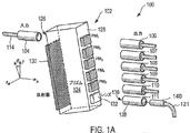
図1A及び図1Bは、一例示のスターカプラ100のそれぞれ等角投影図及び側面図を示している。スターカプラ100は、1:6ビームスプリッタ102、単一の入力コネクタ104及び6つの出力コネクタ106〜111を備える。入力コネクタ104はマルチモード光ファイバ114に接続され、6つの出力コネクタ106〜111はそれぞれマルチモード光ファイバ116〜121に接続されている。スプリッタ102は、第1の表面126及び対向する第2の表面128を有するプリズム124を備える。第1の表面126は、第2の表面128に対してほぼ平行に向いている。また、スプリッタ102は、第1の表面126に配置された反射器130と、反射器130に対向して第2の表面128に配置された、PM1〜PM5によって表記される5つの部分ミラーと、反射器130に対向して第2の表面128に配置された反射防止面132と、を備える。反射器130は、入力コネクタ104に対向し覆われていない部分126を残して、第1の表面126の一部分を覆っている。コネクタ104から出力された光のビームは、この対向する部分を通ってプリズム124に入ることができる。出力コネクタ106〜110は、PM1〜PM5と位置合わせされ、出力コネクタ111は、反射防止面132に位置合わせされる。図1A及び図1Bはデカルト座標系を備え、スプリッタ102及びコネクタ104、106〜111はxy平面内に配置され、スプリッタ102はz軸の回りに角度θだけ入力コネクタ104に向けて傾けられている。
1A and 1B show an isometric view and a side view, respectively, of an
反射器130は単一の平面ミラーとすることもできるし、また、反射器130は曲面ミラーのアレイとすることもできることに留意されたい。各曲面ミラーは、反射光を部分ミラーのうちの1つに向けて再平行化する(re-collimate)。
Note that the
入力コネクタ104及び出力コネクタ106〜111は、それぞれがフェルール及びレンズを備える雌コネクタとすることができる。例えば、図1Bに示すように、コネクタ111は、フェルール138内に取り付けられたレンズ136を備える。光ファイバ114及び116〜121は、コネクタ104及び106〜111内に挿入される雄コネクタを備えることができる。例えば、図1Aは、ファイバ121の終端部を示し、この終端部は、フェルール138から取り外された雄コネクタ140を備える。
The
図2Aは、動作中のスターカプラ100の側面図を示している。光は、光ファイバ114を介してスターカプラ100に入る。この光は、非常に多くの波長分割多重化(「WDM」)電磁放射チャネルからなることができる。「チャネル」は、電磁スペクトルの可視部分及び/又は非可視部分における或る周波数の電磁放射又は特定の周波数を中心とする狭帯域の周波数とすることができる。代替的に、この光は、非常に多くのWDM光信号からなることができる。各「光信号」は、特定のチャネルの振幅若しくは位相、又は、振幅及び位相の組み合わせで、データを符号化する。入力コネクタ104は、光を平行化して、法線202に対する入射角θiでプリズム124に入る入力ビーム201にする。プリズム124は、クラウンガラス(すなわち、屈折率n≒1.52)又は別の好適な屈折率材料から構成することができる。ビーム201は、プリズム124に入ると、法線202に対する屈折角θrでPM1に向けて屈折される。PM1は、ビーム201を内部反射ビーム203及び透過出力ビーム204に分離する。反射ビーム203は、ビーム201の光パワーの第1の部分を含み、透過ビーム204は、ビーム201の光パワーの第2の部分を含む。図2Aに示すように、プリズム124の厚さL、入射角θi、及び部分ミラーPM1〜PM5間の規則的な間隔は、部分ミラーPM1〜PM5と反射器130との間をジグザグパターンで往復反射する内部ジグザグビーム206を形成するように選択される。ビーム206が部分ミラーに当たるごとに、ビーム206の第1の部分は、反射器130に向けて反射され、第2の部分は、対応する出力コネクタに透過する。その結果として、ビーム206は、反射器130と部分ミラーとの間で往復反射するにつれて減衰する。レンズ132は、ビーム206内の光パワーの残りの部分を出力コネクタ111に単に誘導するだけである。
FIG. 2A shows a side view of the
図2Aに示すように、ジグザグビーム206は、当該ビーム206が部分ミラーPM1〜PM5間で往復反射されているとき、平行化された状態を維持する。部分ミラーPM1〜PM5を出力コネクタに向けて通過する透過出力ビームは、比較的平行化された状態を維持しているが、ほぼ円形の断面を維持している。例えば、図2Aは、線I−Iに沿った透過ビーム204の円形断面を含む。出力コネクタ106〜111はそれぞれ、対応する部分ミラーから透過ビームを受信し、それらのビームを、接続された光ファイバ内に集束する。
As shown in FIG. 2A, the
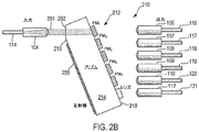
他の例示のスターカプラでは、ビームスプリッタに入力された光が図2Aを参照して上述した方法で屈折されないようにプリズムを構成することができる。図2Bは、一例示のスターカプラ210の側面図を示している。スターカプラ210は、スターカプラ100と同様である。スターカプラ100と同じように、スターカプラ210は、プリズム214を有する1:6ビームスプリッタ212を備え、このプリズムは、反射器220及び部分ミラーがそれぞれ配置されている2つの対向するほぼ平行な第1の表面216及び第2の表面218を有する。しかしながら、スターカプラ100のプリズム124と異なり、プリズム214は、第1の表面216に隣接するとともに第2の表面218に対向する第3の表面222を備える。図2Bの例では、第3の表面222は、当該第3の表面222にほぼ垂直に入射する光のビーム224がプリズム214に入り、PM1に達する際に屈折されないように角度付けられている。
In another exemplary star coupler, the prism can be configured such that light input to the beam splitter is not refracted in the manner described above with reference to FIG. 2A. FIG. 2B shows a side view of an
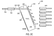
図2Cは、一例示のスターカプラ230の側面図を示している。スターカプラ230は、スターカプラ100と同様である。スターカプラ100と同じように、スターカプラ230は、プリズム234を有する1:6ビームスプリッタ232を備え、このプリズムは、反射器240及び部分ミラーがそれぞれ配置されている2つの対向するほぼ平行な第1の表面236及び第2の表面238を有する。しかしながら、スターカプラ100のプリズム124と異なり、プリズム234は、第1の表面236に隣接するとともに第2の表面238に対向して位置する凸レンズ242を備える。凸レンズ242は、コネクタ104から出力された広がるビーム244を平行化して、PM1に当たる平行ビーム246にする。
FIG. 2C shows a side view of an
他の例では、スプリッタ102及び212の双方に対して、レンズ242を平凸レンズ等の別個の光学素子として実施することができる。この光学素子は、広がるビーム244を集束して、平行ビーム246のような、スプリッタ102のプリズム124又はスプリッタ212のプリズム214に入る平行ビームにするように調整することができる。
In other examples, for both
部分ミラーPM1〜PM5は、サブ波長格子、ポルカドット(polka dot)反射器、誘電体ミラー、又は部分的銀被覆ミラーとすることができる。部分ミラーPM1〜PM5は、プリズムに個別に取り付けられる異なる基材に配置することもできるし、反射防止面とともに単一の基材上に実装することもできる。或るスターカプラの例では、部分ミラーPM1〜PM5は、ほぼ同じ光パワーを有するビームを透過する。図3は、透過出力ビーム301〜306の光パワーが入力ビーム308の光パワーのほぼ1/6になるように構成された部分ミラーPM1〜PM5を有する一例示の1:6ビームスプリッタ300を示している。例えば、入力ビーム308の光パワーがPによって表されるものと仮定する。部分ミラーがほぼ同じ光パワーP/6を有する光を透過するために、PM1は、約5/6(すなわち、5P/6)の反射率と約1/6(すなわち、P/6)の透過率とを有するように構成されている。PM2は、約4/5(すなわち、4/5×5P/6)の反射率と約1/5(すなわち、1/5×5P/6)の透過率とを有するように構成されている。PM3は、約3/4(すなわち、3/4×4P/6)の反射率と約1/4(すなわち、1/4×4P/6)の透過率とを有するように構成されている。PM4は、約2/3(すなわち、2/3×3P/6)の反射率と約1/3(すなわち、1/3×3P/6)の透過率とを有するように構成されている。PM5は、約1/2(すなわち、1/2×2P/6)の反射率と約1/2(すなわち、1/2×2P/6)の透過率とを有する50:50ビームスプリッタとして動作するように構成されている。
The partial mirrors PM 1 to PM 5 can be sub-wavelength gratings, polka dot reflectors, dielectric mirrors, or partial silver-coated mirrors. The partial mirrors PM 1 to PM 5 can be arranged on different substrates that are individually attached to the prisms, or can be mounted on a single substrate together with an antireflection surface. In an example of a star coupler, the partial mirrors PM 1 to PM 5 transmit beams having substantially the same optical power. FIG. 3 illustrates an exemplary 1: 6
スターカプラは、単一のビームを6つの別々のビームに分離することに限定されるものではない。他の例では、スターカプラは、ビームを僅か2つのビームに分離するように構成することもできるし、ビームを3つ、4つ、5つ、又は7つ以上もの多くのビームに分離するように構成することもできる。ビームの最大数は、入力ビームの光パワー、全体的なシステム損失、及び透過ビームを検出するのに用いられる受信機の最小感度によって決定することができる。 A star coupler is not limited to separating a single beam into six separate beams. In other examples, the star coupler can be configured to split the beam into as few as two beams, or to split the beam into as many as three, four, five, seven or more beams. It can also be configured. The maximum number of beams can be determined by the optical power of the input beam, the overall system loss, and the minimum sensitivity of the receiver used to detect the transmitted beam.
一般に、ビームスプリッタプリズムの表面に沿って分散された部分ミラーは、光パワーPのビームがプリズムに入ると、各透過ビームが約P/Nの光パワーでスプリッタを出るように構成することができる。ここで、Nは透過ビームの数である。図4は、一例示の1:Nビームスプリッタ400を示している。スプリッタ400は、第1の表面404及び第2の表面406を有するプリズム402を備える。これらの第1の表面及び第2の表面は、互いに対してほぼ平行に向いている。スプリッタ400は、第1の表面404に配置された反射器408を備え、第2の表面406に配置された部分ミラーPM1〜PMN−1及び反射防止面410を備える。これらの部分ミラーは、方向矢印411〜418によって表される各透過出力ビームがP/Nのほぼ同じ光パワーを有するように構成されている。ここで、Pは、入力ビーム420の光パワーである。一般に、PMmによって表記される部分ミラーは、下記の式によって与えられる透過率を有し、
![]()

![]()
代替的なビームスプリッタの実施態様では、プリズム及び反射器は、部分ミラーの数に対応する曲面と、反射防止面とを有するように構成することができることに留意されたい。これらの曲面及び曲面反射器は、部分ミラー及び反射防止面に反射された各光のビームを内部で再平行化する。 Note that in alternative beam splitter embodiments, the prisms and reflectors can be configured to have curved surfaces corresponding to the number of partial mirrors and anti-reflection surfaces. These curved surfaces and curved reflectors internally re-parallelize the beams of light reflected by the partial mirror and the antireflection surface.
スターカプラのビームスプリッタ及びコネクタは、スプリッタ及びコネクタの位置を固定する筐体(図示せず)内に取り付けられ、各コネクタとスプリッタとの間に一定の離隔距離を維持し、スプリッタの向きを固定する。この筐体によって、スプリッタ及び既に挿入されている他のファイバの位置を乱すことなくファイバの選択的な取り外し及び挿入を行うことが可能になる。例えば、スターカプラ100に光学的に接続されて、出力コネクタ106〜111を通って出力される6つの光信号又は未変調チャネルのうちの1つを受信することができるデバイスの数は1〜6の範囲である。換言すれば、スターカプラ100によって、光学的に接続されて光信号又はチャネルを受信するデバイスの数を、デバイスの光ファイバを単に接続又は接続解除するだけで選択的に増大又は縮小することが可能になる。
The star coupler beam splitter and connector are mounted in a housing (not shown) that fixes the position of the splitter and connector, maintaining a fixed separation distance between each connector and the splitter, and fixing the orientation of the splitter. To do. This housing allows selective removal and insertion of fibers without disturbing the position of the splitter and other fibers already inserted. For example, the number of devices optically connected to the
1:Nスターカプラは、ノードからなるシステム内のノードが光信号を他のノードにブロードキャストすることを可能にする光相互接続ファブリックに実装することができる。ノードは、プロセッサ、メモリ、メモリコントローラ、電気/光エンジン、光/電気エンジン、マルチコア処理ユニットのクラスタ、回路基板、外部ネットワーク接続、又は他の任意のデータ処理デバイス、記憶デバイス、若しくは送信デバイスの任意の組み合わせとすることができる。 1: N star couplers can be implemented in an optical interconnect fabric that allows nodes in a system of nodes to broadcast optical signals to other nodes. A node can be a processor, memory, memory controller, electrical / light engine, light / electric engine, cluster of multi-core processing units, circuit board, external network connection, or any other data processing device, storage device, or transmission device It can be set as a combination.
図5は、各ノードが光相互接続ファブリックに接続されている一例示のNノードシステムを示している。これらのノードには、1〜Nのラベルが付けられている。便宜上、図5は、3つのN光相互接続ファブリック501〜503しか示していない。光相互接続ファブリック501は、1:Nスターカプラ504と、第1の端がスターカプラ504に接続され、第2の端がノード1における電気/光(「EO」)変換器506に接続されている単一のマルチモード入力光ファイバ505と、N個のマルチモード出力光ファイバ508とを備える。これらのマルチモード出力光ファイバのそれぞれは、第1の端がスターカプラ504に接続され、第2の端がOE変換器510等の、N個のノードのうちの1つにおける光/電気(「OE」)変換器に接続されている。ファイバ505は、ノード1から光信号を送信するのに用いられ、図1に示す1:6スターカプラ100の入力コネクタ104のようなスターカプラ504の入力コネクタ(図示せず)に接続され、N個の光ファイバ508のそれぞれは、1:6スターカプラ100の出力コネクタ106〜111のようなスターカプラ504の出力コネクタ(図示せず)に接続されている。ファイバ508は、スターカプラ504から出力された光信号を受信する。ファブリック501は、以下のように、ノード1が光信号をノード1〜Nにブロードキャストすることを可能にする。ノード1は、データを電子信号の形式で生成する。このデータは、EO変換器506において光パワーPを有する光信号に変換される。この光信号は、ファイバ505に入力され、スターカプラ504に送信される。スターカプラ504は、光信号をN個の別々の光信号に分離するスプリッタ400のような1:Nビームスプリッタを備える。光信号のそれぞれは、同じデータを符号化しており、図4を参照して上述したように、同じ光パワーP/Nで1:Nビームスプリッタを出る。N個の光信号のそれぞれは、図3を参照して上述したように、出力コネクタを介して光ファイバ508のうちの1つに入り、N個のノードのうちの1つに送信される。ノードでは、OE変換器が、光信号を、そのノードにおいて処理することができる電子信号に変換する。
FIG. 5 illustrates an example N-node system in which each node is connected to an optical interconnect fabric. These nodes are labeled 1-N. For convenience, FIG. 5 shows only three N optical interconnect fabrics 501-503. The
光相互接続ファブリック502は、当該ファブリック502がノード2を1:Nスターカプラ512に接続するマルチモード光ファイバ510を備えることを除いて、ファブリック501と同様である。ファブリック502は、ノード1が光信号をファブリック501によってノード1〜Nにブロードキャストするのと同じ方法で、ノード2が光信号をノード1〜Nにブロードキャストすることを可能にする。光相互接続ファブリック503も、当該ファブリック503がノードNを1:Nスターカプラ516に接続するマルチモード光ファイバ514を備えることを除いて、ファブリック501と同様である。ファブリック503は、ノード1が光信号をファブリック501によってノード1〜Nにブロードキャストするのと同じ方法で、ノードNが光信号をノード1〜Nにブロードキャストすることを可能にする。
The
上述した光相互接続ファブリックの例及び後述する光相互接続ファブリックの例は、ノードによって生成された光信号をその発信源のノードに誘導して戻していることに留意されたい。これは、2つの主な理由によって行われる。すなわち、1)誘導して戻すことによって、スターカプラが正常に動作していることが保証される。2)光信号を、それらが発信されたノードに方向転換して戻すことによって、そのノードは、当該光信号に対して、光信号完全性テスト等の診断テストを実行することができる。 Note that the example optical interconnect fabric described above and the example optical interconnect fabric described below directs the optical signal generated by a node back to its originating node. This is done for two main reasons. That is, 1) By guiding back, it is ensured that the star coupler is operating normally. 2) By redirecting optical signals back to the node from which they originated, the node can perform diagnostic tests, such as an optical signal integrity test, on the optical signals.
N個の光相互接続ファブリックは、ブレードシステムのバックプレーンに実装することができ、これによって、ブレードシステム内の各ブレードは、光信号をシステム内の他のブレードにブロードキャストすることが可能になる。ブレードシステムは、サーバブレード又はブレードとして知られている複数のモジュール電子回路基板を収容するサーバシャーシである。複数のブレードを保持することができるサーバシャーシ又はブレード筐体は、電力、冷却、ネットワーク化、様々な相互接続、及びブレード管理、等のサービスを提供する。各ブレードは、少なくとも1つのプロセッサ、メモリ、統合ネットワークコントローラ、及び他の入出力ポートで構成されることができ、各ブレードは、ローカルドライブを有するように構成することもでき、ネットワークアタッチト・ストレージ、ファイバチャネル、又はiSCSIストレージエリアネットワークによって容易にされるストレージプールに接続することができる。 N optical interconnect fabrics can be implemented on the backplane of the blade system, which allows each blade in the blade system to broadcast optical signals to other blades in the system. A blade system is a server chassis that houses a plurality of module electronic circuit boards known as server blades or blades. A server chassis or blade enclosure that can hold multiple blades provides services such as power, cooling, networking, various interconnections, and blade management. Each blade can be configured with at least one processor, memory, integrated network controller, and other input / output ports, and each blade can also be configured with local drives, network attached storage Can be connected to a storage pool facilitated by a Fiber Channel or iSCSI storage area network.
図6Aは、ブレード筐体又はシャーシ608内に取り付けられた6つのブレード601〜606からなる一例示のブレードシステム600の等角投影図を示している。各ブレードは、ブレード間の入出力光接続性を提供するバックプレーン610に接続されている。図6Bは、この例示のシステム600のバックプレーンを示している。図6Bの例では、バックプレーン610は、破線の筐体611〜616によって識別される6つの別々の光相互接続ファブリックを備える。方向矢印が光ファイバを表すのに用いられ、その方向の光信号が光ファイバを移動する(traverse)。各光相互接続ファブリックは、1:6スターカプラを備える。例えば、光相互接続ファブリック611は、ブレード601が光信号をブレード601〜606にブロードキャストすることを可能にする。ブレード601によって生成された電子信号は、EO変換器618において、ファイバ620をスターカプラ622まで移動する光信号に変換される。スターカプラ622は、上述したスターカプラ100、210、及び230と同じ方法で動作するように構成することができる。光信号は、平行化され、6つの別々の光信号に分離される。ほぼ同じ光パワーを有する6つの光信号は、同じデータを符号化しており、各光信号は、6つの別々のマルチモードファイバ624〜629のうちの1つに入る。これらの光信号はそれぞれ、対応するOE変換器において電子信号に変換される。例えば、OE変換器630は、ファイバ629において送信された光信号を、ブレード606によって処理することができる電子信号に変換する。マルチバスファブリック612〜616はそれぞれ同じ方法で動作して、ブレード602〜606によってそれぞれ生成された光信号をブロードキャストする。
FIG. 6A shows an isometric view of an
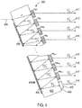
スターカプラは、単一の入力において光を受信してその光をN個の出力に分離することに限定されるものではない。スターカプラは、M個の別々の入力において光を受信して、各入力において受信した光をN個の出力に分離するように構成することができ、M:M×Nスターカプラと呼ばれる。図7は、一例示のスターカプラ700の等角投影図を示している。スターカプラ700は、4つの入力コネクタ701〜704(すなわち、M=4)の1次元アレイと、出力コネクタ706等の24個の出力コネクタ(すなわち、N=6)の2次元アレイとを備える。4つの入力コネクタ701〜704は、4つの別々のコネクタとすることもできるし、リボンファイバコネクタとすることもできる。スターカプラ700は、4:4×6ビームスプリッタ708も備える。スプリッタ708は、対向するほぼ平行な第1の表面712及び第2の表面714を有するプリズム710を備える。図7の例に示すように、反射器716が、覆われていない部分718を残して、第1の表面712の一部分に配置されている。また、スプリッタ708は、z方向に延在する5つの部分ミラー721〜725と、第2の表面714に配置された反射防止被覆ストリップ726とを備える。図7の例では、部分ミラーは、図2を参照して上述した部分ミラーPM1〜PM5と同じ方法で光を反射及び透過するように構成されている。部分ミラーは、プリズム710に個別に取り付けられる異なる基材に配置することもできるし、部分ミラーは、反射防止面とともに単一の基材上に実装することもできる。
A star coupler is not limited to receiving light at a single input and separating the light into N outputs. A star coupler can be configured to receive light at M separate inputs and separate the received light at each input into N outputs, referred to as an M: M × N star coupler. FIG. 7 shows an isometric view of an
反射器716は、単一の平面ミラーとすることもできるし、また、反射器716は、曲面ミラーのアレイとすることもできることに留意されたい。各曲面ミラーは、反射光を部分ミラーのうちの1つに向けて再平行化する。
Note that the
入力コネクタと、部分ミラー及び反射防止面の列と、出力コネクタの列とが、図1〜図3を参照して上述したスターカプラが光のビームを分離するのと同じ方法で、光のビームを分離する。例えば、図7に示すように、入力コネクタ701は、光のビーム720を、プリズム710の覆われてない部分718を通ってスプリッタ708内に誘導する。このビームは、図3を参照して上述したように、部分ミラーの列と反射器716との間で往復反射する。光のビームは、ほぼ同じ光パワーで列内の部分ミラー及び反射防止面から出力される。図7に示すように、入力コネクタ701〜704は、光の入力ビームをプリズム710に平行に誘導し、部分ミラー及び反射防止面は、出力コネクタと位置合わせされており、そのため、部分ミラーから出力されたビームはほぼ平行であり、各ビームは対応する出力コネクタ内に誘導される。光の入力ビーム及び出力ビームは、同じ方向に送信される。入力コネクタ及び出力コネクタは、図1を参照して上述したように、それぞれがフェルール及びレンズを備える雌コネクタとすることができる。光ファイバは、スターカプラの雌コネクタ内に挿入される雄コネクタも備えることができる。
The input connector, the row of partial mirrors and the anti-reflection surface, and the row of output connectors, in the same way that the star coupler described above with reference to FIGS. Isolate. For example, as shown in FIG. 7, the
M:M×Nスターカプラは、ノードからなるシステム内のノードが光信号を他のノードにブロードキャストすることを可能にする光相互接続ファブリックに実装することができる。図8は、3つのノードが光相互接続ファブリック800に接続されている一例示のNノードシステムを示している。ファブリック800は、3:3×Nスターカプラ802及び3つのマルチモード入力光ファイバ804〜806を備える。これらのマルチモード入力光ファイバのそれぞれは、第1の端がスターカプラ802に接続され、第2の端が3つのEO変換器808〜810のうちの1つに接続されている。ファブリック800は、N個のマルチモード出力光ファイバ812も備える。これらのマルチモード出力光ファイバのそれぞれは、第1の端がスターカプラ802に接続され、第2の端が、OE変換器814等の、N個のノードのうちの1つにおけるOE変換器に接続されている。ファイバ804〜806は、スターカプラ802の入力コネクタ(図示せず)に接続され、N個の光ファイバ812のそれぞれは、スターカプラ802の出力コネクタ(図示せず)に接続されている。ファブリック800は、図5を参照して上述したように、ノード1〜3のそれぞれが光信号をノード1〜Nにブロードキャストすることを可能にする。
An M: M × N star coupler can be implemented in an optical interconnect fabric that allows nodes in a system of nodes to broadcast optical signals to other nodes. FIG. 8 shows an exemplary N-node system with three nodes connected to the
図9は、N個のノードが光相互接続ファブリック900に接続されている一例示のNノードシステムを示している。ファブリック900は、N:N×Nスターカプラ902及びN個のマルチモード入力光ファイバ904を備える。これらのマルチモード入力光ファイバのそれぞれは、第1の端がスターカプラ902に接続され、第2の端が、EO変換器906等の、N個のEO変換器のうちの1つに接続されている。ファブリック900は、N個のマルチモード出力光ファイバ908も備える。これらのマルチモード出力光ファイバのそれぞれは、第1の端がスターカプラ902に接続され、第2の端が、OE変換器910等の、N個のノードのうちの1つにおけるOE変換器に接続されている。ファブリック900は、図5を参照して上述したように、N個のノードのそれぞれが光信号をノード1〜Nにブロードキャストすることを可能にする。
FIG. 9 shows an exemplary N-node system in which N nodes are connected to the
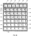
M:M×Nスターカプラは、ブレードシステムのバックプレーンに実装することができる。図10は、例示のブレードシステム600の一例示のバックプレーン1000を示している。バックプレーン1000は、2つの別々の光相互接続ファブリック1002及び1004を備える。光相互接続ファブリック1002は4:4×6スターカプラ1006を備え、光相互接続ファブリック1004は2:2×6スターカプラ1008を備える。光相互接続ファブリック1002は、ブレード601〜604が光信号をブレード601〜606にブロードキャストすることを可能にし、光相互接続ファブリック1004は、ブレード605及び606が光信号をブレード601〜606にブロードキャストすることを可能にする。ブレードが光信号をブロードキャストするのに用いる数組の光ファイバを表すのに、種々のラインパターンが用いられている。例えば、実線の方向矢印1010は、ブレード601が光信号をブレード601〜606にブロードキャストするのに用いる光ファイバを表し、破線の方向矢印1012は、ブレード606が光信号をブレード601〜606にブロードキャストするのに用いる光ファイバを表している。各ブレードは、光信号を、図6を参照して上述した方法でブロードキャストする。
The M: M × N star coupler can be mounted on the backplane of the blade system. FIG. 10 illustrates an
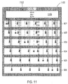
図11は、上記例示のブレードシステム600の一例示のバックプレーン1100を示している。バックプレーン1100は、単一の光相互接続ファブリック1102を備える。光相互接続ファブリック1102は、ブレード601〜606が光信号を当該ブレード601〜606にブロードキャストすることを可能にする6:6×6スターカプラ1104を備える。各ブレードは、図6を参照して上述した方法で、光信号を対応する一組の光ファイバによってブロードキャストする。
FIG. 11 illustrates an
本開示を十分に理解してもらうために、説明の便宜上、これまでの説明は特有の用語を使用した。しかしながら、本明細書に記載されたシステム及び方法を実践するために、具体的な細部が不要であることは当業者には明らかであろう。具体的な実施形態のこれまでの説明は、例示し、説明するために提示されている。それらの実施形態は、本開示を網羅することも、本開示を開示されるのと全く同じ形に限定することも意図していない。上記の教示に鑑みて、明らかに、数多くの変更及び変形が可能である。それらの実施形態は、本開示の原理及びその実用的な応用例を最もわかりやすく説明し、それにより、意図した特定の用途に相応しいように種々の変更を加えながら、当業者が本開示及び種々の実施形態を最大限に利用できるようにするために、図示及び説明されている。本開示の範囲は、添付の特許請求の範囲及びその均等物によって規定されることが意図されている。
In order to provide a thorough understanding of the present disclosure, specific terminology has been used in the previous description for convenience of description. However, it will be apparent to one skilled in the art that the specific details are not required in order to practice the systems and methods described herein. The foregoing description of specific embodiments has been presented for purposes of illustration and description. These embodiments are not intended to be exhaustive or to limit the present disclosure to the precise form disclosed. Obviously, many modifications and variations are possible in view of the above teachings. These embodiments best illustrate the principles of the present disclosure and its practical applications, so that those skilled in the art can make various changes and modifications to suit the particular intended use. In order to make the most possible use of this embodiment, it is shown and described. It is intended that the scope of the disclosure be defined by the appended claims and their equivalents.
Claims (15)
光の入力ビームを前記スターカプラ内に誘導する入力コネクタ(104、701〜704)と、
複数の出力コネクタ(106〜111、706)と、
を備え、
前記スターカプラは、前記入力ビームを、同じ光パワーで該スターカプラを出る複数の平行な出力ビームに分離し、各出力ビームは、前記出力コネクタのうちの1つに入る、光カプラ。 A star coupler (102, 708);
An input connector (104, 701-704) for directing an input beam of light into the star coupler;
A plurality of output connectors (106-111, 706);
With
The star coupler splits the input beam into a plurality of parallel output beams exiting the star coupler with the same optical power, each output beam entering one of the output connectors.
第1の表面(126、712)と、該第1の表面に対向して位置する第2の表面(128、714)とを有するプリズム(124、710)と、
前記第1の表面の一部分に配置された反射器(130、716)と、
前記第2の表面に配置された複数の部分ミラーと、
前記第2の表面に配置された反射防止面(132)と、
を更に備え、
各入力ビームは、前記第1の表面を通って前記スターカプラに入り、前記反射器と前記部分ミラーとの間で往復反射してジグザグビームを形成し、各出力ビームが、前記部分ミラーのうちの1つ又は前記反射防止面を通って透過する、前記ジグザグビームの一部分であるようになっている、請求項1に記載のカプラ。 The star coupler is
A prism (124, 710) having a first surface (126, 712) and a second surface (128, 714) located opposite the first surface;
A reflector (130, 716) disposed on a portion of the first surface;
A plurality of partial mirrors disposed on the second surface;
An antireflection surface (132) disposed on the second surface;
Further comprising
Each input beam enters the star coupler through the first surface and reciprocally reflects between the reflector and the partial mirror to form a zigzag beam, and each output beam is out of the partial mirror. The coupler of claim 1, wherein the coupler is a portion of the zigzag beam that is transmitted through one of the antireflection surfaces.
複数の出力光ファイバ(508、812)であって、各出力光ファイバは、第1の端が前記スターカプラに接続され、第2の端が複数のノードのうちの1つのノードに接続されている、複数の出力光ファイバと、
第1の端が前記スターカプラ(504、802)に接続され、第2の端が前記複数のノードのうちの1つのノードに接続されている入力光ファイバ(505、804〜806)と、
を備え、
前記スターカプラは、前記入力光ファイバを介して少なくとも1つの光信号を受信し、各光信号を、同じ光パワーを有する複数の光信号に分離し、各光信号を前記出力光ファイバのうちの1つに出力する、光相互接続ファブリック。 A star coupler (504, 802);
A plurality of output optical fibers (508, 812), each output optical fiber having a first end connected to the star coupler and a second end connected to one of the plurality of nodes; A plurality of output optical fibers; and
An input optical fiber (505, 804-806) having a first end connected to the star coupler (504, 802) and a second end connected to one of the plurality of nodes;
With
The star coupler receives at least one optical signal via the input optical fiber, separates each optical signal into a plurality of optical signals having the same optical power, and separates each optical signal from the output optical fiber. An optical interconnect fabric that outputs to one.
スターカプラ(102、708)と、
入力コネクタ(104、701〜704)であって、各入力コネクタは、前記入力光ファイバの前記第1の端に接続されて、前記入力光ファイバによって搬送された前記光信号を前記スターカプラ内に誘導する、入力コネクタと、
複数の出力コネクタ(106〜111、706)であって、各出力コネクタは、前記出力光ファイバの前記第1の端に接続されている、複数の出力コネクタと、
を更に備え、
前記スターカプラは、前記光信号を、同じ光パワーを有する前記複数の光信号に分離し、各光信号は、前記出力コネクタのうちの1つに入る、請求項7に記載のファブリック。 The star coupler is
A star coupler (102, 708);
Input connectors (104, 701 to 704), each input connector being connected to the first end of the input optical fiber, and passing the optical signal carried by the input optical fiber into the star coupler An input connector to guide,
A plurality of output connectors (106-111, 706), each output connector connected to the first end of the output optical fiber;
Further comprising
The fabric of claim 7, wherein the star coupler separates the optical signal into the plurality of optical signals having the same optical power, each optical signal entering one of the output connectors.
第1の表面(126、712)と、該第1の表面に対向して位置する第2の表面(128、714)とを有するプリズム(124、710)と、
前記第1の表面の一部分に配置された反射器(130、716)と、
前記第2の表面に配置された複数の部分ミラーと、
前記第2の表面に配置された反射防止面(132)と、
を更に備え、
各光信号は、前記第1の表面を通って前記スターカプラに入り、前記反射器と前記部分ミラーとの間で往復反射してジグザグビームを形成し、前記スターカプラから出力される各光信号が、前記部分ミラーのうちの1つ又は前記反射防止面を通って透過する、前記ジグザグビームの一部分であるようになっている、請求項12に記載のファブリック。 The star coupler is
A prism (124, 710) having a first surface (126, 712) and a second surface (128, 714) located opposite the first surface;
A reflector (130, 716) disposed on a portion of the first surface;
A plurality of partial mirrors disposed on the second surface;
An antireflection surface (132) disposed on the second surface;
Further comprising
Each optical signal enters the star coupler through the first surface, reciprocally reflects between the reflector and the partial mirror to form a zigzag beam, and is output from the star coupler. 13. The fabric of claim 12, wherein the fabric is a portion of the zigzag beam that is transmitted through one of the partial mirrors or the anti-reflective surface.
Each output connector further comprises a lens (136) mounted in a ferrule (138) that receives one of the plurality of output optical fibers, and an optical signal enters the output connector through the lens; The fabric of claim 12, wherein the fabric is focused within a core of the optical fiber.
Applications Claiming Priority (1)
| Application Number | Priority Date | Filing Date | Title |
|---|---|---|---|
| PCT/US2010/054774 WO2012057792A1 (en) | 2010-10-29 | 2010-10-29 | Optical interconnect fabrics implemented with star couplers |
Publications (1)
| Publication Number | Publication Date |
|---|---|
| JP2014500977A true JP2014500977A (en) | 2014-01-16 |
Family
ID=45994257
Family Applications (1)
| Application Number | Title | Priority Date | Filing Date |
|---|---|---|---|
| JP2013536579A Pending JP2014500977A (en) | 2010-10-29 | 2010-10-29 | Optical interconnect fabric implemented using star couplers |
Country Status (3)
| Country | Link |
|---|---|
| US (1) | US20130216180A1 (en) |
| JP (1) | JP2014500977A (en) |
| WO (1) | WO2012057792A1 (en) |
Families Citing this family (15)
| Publication number | Priority date | Publication date | Assignee | Title |
|---|---|---|---|---|
| KR102110121B1 (en) * | 2012-04-26 | 2020-05-13 | 휴렛 팩커드 엔터프라이즈 디벨롭먼트 엘피 | Optical slab |
| KR20150015470A (en) * | 2012-05-24 | 2015-02-10 | 휴렛-팩커드 디벨롭먼트 컴퍼니, 엘.피. | Fiber connector assembly |
| JP2015102796A (en) * | 2013-11-27 | 2015-06-04 | セイコーエプソン株式会社 | Optical branching device |
| DE102015105446A1 (en) * | 2014-04-24 | 2015-10-29 | Gtran Inc. | Wavelength Multiplexing Device (WDM) and De-Multiplexing Device (WDDM) |
| CN104020527A (en) * | 2014-06-11 | 2014-09-03 | 武汉电信器件有限公司 | Multichannel integrated optical wavelength division multiplexing/demultiplexing component structure |
| US10656013B2 (en) | 2015-09-29 | 2020-05-19 | Chromation Inc. | Nanostructure based article, optical sensor and analytical instrument and method of forming same |
| US20230296853A9 (en) | 2015-10-08 | 2023-09-21 | Teramount Ltd. | Optical Coupling |
| EP3745605B1 (en) | 2016-03-22 | 2022-08-24 | Lyteloop Technologies, Llc | Data in motion storage system and method |
| CN109313075B (en) * | 2016-05-10 | 2020-10-30 | 施罗玛蒂奥尼有限公司 | Integration of optical components within folded optical circuits |
| US20170346553A1 (en) * | 2016-05-27 | 2017-11-30 | Corning Optical Communications LLC | Fiber optic assemblies for tapping live optical fibers in fiber optic networks employing wdm technology |
| FR3060248B1 (en) * | 2016-12-09 | 2019-03-15 | Safran Electrical & Power | OPTICAL RING OPERATED COMMUNICATION NETWORK FOR AIRCRAFT |
| US11361794B2 (en) * | 2018-08-02 | 2022-06-14 | Lyteloop Technologies, Llc | Apparatus and method for storing wave signals in a cavity |
| MX2020009303A (en) | 2018-08-10 | 2022-03-22 | Lyteloop Tech Llc | System and method for extending path length of a wave signal using angle multiplexing. |
| WO2020096912A1 (en) | 2018-11-05 | 2020-05-14 | Lyteloop Technologies, Llc | Systems and methods for building, operating and controlling multiple amplifiers, regenerators and transceivers using shared common components |
| WO2022076438A1 (en) * | 2020-10-06 | 2022-04-14 | Chromation Inc. | Systems and methods to redistribute field of view in spectroscopy |
Citations (11)
| Publication number | Priority date | Publication date | Assignee | Title |
|---|---|---|---|---|
| JPH05333288A (en) * | 1992-06-01 | 1993-12-17 | Nippon Telegr & Teleph Corp <Ntt> | Optical star coupler |
| JPH07307739A (en) * | 1994-05-13 | 1995-11-21 | Canon Inc | Information sharing method, line allocation method and communication system using the same |
| US6008920A (en) * | 1998-03-11 | 1999-12-28 | Optical Coating Laboratory, Inc. | Multiple channel multiplexer/demultiplexer devices |
| JP2001156371A (en) * | 1999-11-24 | 2001-06-08 | Communication Research Laboratory Mpt | Optical branching method |
| US20030002101A1 (en) * | 2001-07-02 | 2003-01-02 | Jorg-Reinhardt Kropp | Device and method for multiplexing and/or demultiplexing optical signals of a plurality of wavelengths |
| JP2003107276A (en) * | 2001-10-01 | 2003-04-09 | Matsushita Electric Ind Co Ltd | Optical fiber collimator, lens for optical fiber collimator and optical coupling parts |
| JP2006023500A (en) * | 2004-07-07 | 2006-01-26 | Matsushita Electric Ind Co Ltd | Wavelength division multiplexing coupler |
| JP2006520491A (en) * | 2003-03-14 | 2006-09-07 | アジレント・テクノロジーズ・インク | Small form factor all-polymer optical device with integrated dual beam path based on bending light with total reflection |
| WO2006134675A1 (en) * | 2005-06-14 | 2006-12-21 | Nippon Telegraph And Telephone Corporation | Optical multiplexer/demultiplexer and assembling device thereof |
| JP2007322859A (en) * | 2006-06-02 | 2007-12-13 | Nippon Telegr & Teleph Corp <Ntt> | Optical multiplexer/demultiplexer |
| JP2009177037A (en) * | 2008-01-28 | 2009-08-06 | National Institute Of Information & Communication Technology | Light branching device and its method |
Family Cites Families (44)
| Publication number | Priority date | Publication date | Assignee | Title |
|---|---|---|---|---|
| US4428046A (en) * | 1980-05-05 | 1984-01-24 | Ncr Corporation | Data processing system having a star coupler with contention circuitry |
| JPS6019101A (en) * | 1983-07-13 | 1985-01-31 | Hoya Corp | Beam splitter |
| DE3413703A1 (en) * | 1984-04-12 | 1985-10-24 | Standard Elektrik Lorenz Ag, 7000 Stuttgart | OPTICAL MULTIPLEXER / DEMULTIPLEXER |
| JPS6323105A (en) * | 1986-02-06 | 1988-01-30 | Fujitsu Ltd | Optical multiplexer/demultiplexer |
| US5165080A (en) * | 1987-09-11 | 1992-11-17 | British Telecommunications Public Limited Company | Optical distributor |
| US5127067A (en) * | 1990-09-10 | 1992-06-30 | Westinghouse Electric Corp. | Local area network with star topology and ring protocol |
| US5282257A (en) * | 1990-12-28 | 1994-01-25 | Fuji Xerox Co., Ltd. | Star coupler and optical communication network |
| EP0560043B1 (en) * | 1992-03-07 | 1997-06-18 | Minnesota Mining And Manufacturing Company | Manufacturing method of devices for lightguide networks and elements produced using this method |
| US5583683A (en) * | 1995-06-15 | 1996-12-10 | Optical Corporation Of America | Optical multiplexing device |
| US5894535A (en) * | 1997-05-07 | 1999-04-13 | Hewlett-Packard Company | Optical waveguide device for wavelength demultiplexing and waveguide crossing |
| CA2238606A1 (en) * | 1997-06-26 | 1998-12-26 | Michael Anthony Scobey | Cascaded optical multiplexing devices |
| JP2002501212A (en) * | 1998-01-05 | 2002-01-15 | コーニング・インコーポレーテッド | Add / drop optical multiplexing device |
| JP2000147306A (en) * | 1998-08-31 | 2000-05-26 | Kokusai Electric Co Ltd | Wavelength region multiple light beam star coupler, communication station and light transmission system |
| WO2000055663A1 (en) * | 1999-03-15 | 2000-09-21 | Visionex, Inc. | Optical networking assembly |
| JP2001141924A (en) * | 1999-11-16 | 2001-05-25 | Matsushita Electric Ind Co Ltd | Branching device and branching light-receiving element |
| JP2002072010A (en) * | 2000-09-05 | 2002-03-12 | Nippon Sheet Glass Co Ltd | Optical device having wavelength selectivity |
| US7062174B2 (en) * | 2001-01-22 | 2006-06-13 | Essex Corporation | Wavelength division multiplexing add-drop multiplexer using an optical tapped delay line |
| US6735224B2 (en) * | 2001-03-01 | 2004-05-11 | Applied Optoelectronics, Inc. | Planar lightwave circuit for conditioning tunable laser output |
| US6819871B1 (en) * | 2001-03-16 | 2004-11-16 | 4 Wave, Inc. | Multi-channel optical filter and multiplexer formed from stacks of thin-film layers |
| KR20030000285A (en) * | 2001-06-23 | 2003-01-06 | 삼성전자 주식회사 | Wavelength division multiplexer using planar lightwave circuit |
| JP3517406B2 (en) * | 2001-10-10 | 2004-04-12 | サンテック株式会社 | Wavelength variable multiplexer / demultiplexer and wavelength routing device |
| JP3784701B2 (en) * | 2001-11-20 | 2006-06-14 | 株式会社日立製作所 | Optical circuit member and optical transceiver |
| US20030215240A1 (en) * | 2002-04-03 | 2003-11-20 | Grann Eric B. | Optical WDM with single mode tolerance and low profile |
| US20030206688A1 (en) * | 2002-05-03 | 2003-11-06 | Hollars Dennis R. | Miniature optical multiplexer/de-multiplexer DWDM device |
| US7236660B2 (en) * | 2002-05-20 | 2007-06-26 | Jds Uniphase Corporation | Reconfigurable optical add-drop module, system and method |
| JP2004013113A (en) * | 2002-06-11 | 2004-01-15 | Sumitomo Electric Ind Ltd | Optical signal processor |
| US20040005115A1 (en) * | 2002-07-02 | 2004-01-08 | Luo Xin Simon | Optoelectronic add/drop multiplexer |
| US7203422B2 (en) * | 2002-12-26 | 2007-04-10 | Nippon Telegraph And Telephone Corporation | Optical network unit, wavelength splitter, and optical wavelength-division multiplexing access system |
| US7212343B1 (en) * | 2003-07-11 | 2007-05-01 | Alliance Fiber Optic Products, Inc. | Compact wavelength multiplexer/demultiplexer and method for making the same |
| US7058257B2 (en) * | 2003-12-30 | 2006-06-06 | Lightwaves 2020, Inc. | Miniature WDM add/drop multiplexer and method of manufacture thereof |
| US7099528B2 (en) * | 2004-01-07 | 2006-08-29 | International Business Machines Corporation | Methods and devices for coupling electromagnetic radiation using diffractive optical elements |
| US7349602B2 (en) * | 2004-10-08 | 2008-03-25 | Agilent Technologies, Inc. | Wavelength division multiplexer architecture |
| US20060251421A1 (en) * | 2005-05-09 | 2006-11-09 | Ben Gurion University Of The Negev, Research And Development Authority | Improved free space optical bus |
| US7684705B2 (en) * | 2005-10-20 | 2010-03-23 | Fujitsu Limited | Distribution node for a wavelength-sharing network |
| US7639946B2 (en) * | 2006-01-06 | 2009-12-29 | Fujitsu Limited | Distribution node for an optical network |
| US20080031625A1 (en) * | 2006-07-28 | 2008-02-07 | Ryousuke Okuda | WDM hybrid splitter module |
| US8233798B2 (en) * | 2007-09-25 | 2012-07-31 | Levinson Frank H | Parallel transmission of data streams in a star-configured network |
| US7962036B1 (en) * | 2007-10-29 | 2011-06-14 | Lockheed Martin Corporation | Fiber optic network adjustment |
| CN102461019A (en) * | 2009-05-06 | 2012-05-16 | 惠普开发有限公司 | Bus-based scalable optical fabrics |
| WO2011115624A1 (en) * | 2010-03-19 | 2011-09-22 | Hewlett-Packard Development Company, L.P. | Optical star coupler |
| CN102985860A (en) * | 2010-05-19 | 2013-03-20 | 惠普发展公司,有限责任合伙企业 | Optical interconnect fabrics and optical switches |
| US8391717B2 (en) * | 2010-05-24 | 2013-03-05 | Hewlett-Packard Development Company, L. P. | Flow-control methods and systems for multibus systems |
| JP5690411B2 (en) * | 2010-10-27 | 2015-03-25 | ヒューレット−パッカード デベロップメント カンパニー エル.ピー.Hewlett‐Packard Development Company, L.P. | Receiver and transceiver for optical multibus system |
| EP2745164A4 (en) * | 2011-09-30 | 2015-05-20 | Hewlett Packard Development Co | Optical power splitter including a zig-zag |
-
2010
- 2010-10-29 US US13/881,134 patent/US20130216180A1/en not_active Abandoned
- 2010-10-29 WO PCT/US2010/054774 patent/WO2012057792A1/en active Application Filing
- 2010-10-29 JP JP2013536579A patent/JP2014500977A/en active Pending
Patent Citations (11)
| Publication number | Priority date | Publication date | Assignee | Title |
|---|---|---|---|---|
| JPH05333288A (en) * | 1992-06-01 | 1993-12-17 | Nippon Telegr & Teleph Corp <Ntt> | Optical star coupler |
| JPH07307739A (en) * | 1994-05-13 | 1995-11-21 | Canon Inc | Information sharing method, line allocation method and communication system using the same |
| US6008920A (en) * | 1998-03-11 | 1999-12-28 | Optical Coating Laboratory, Inc. | Multiple channel multiplexer/demultiplexer devices |
| JP2001156371A (en) * | 1999-11-24 | 2001-06-08 | Communication Research Laboratory Mpt | Optical branching method |
| US20030002101A1 (en) * | 2001-07-02 | 2003-01-02 | Jorg-Reinhardt Kropp | Device and method for multiplexing and/or demultiplexing optical signals of a plurality of wavelengths |
| JP2003107276A (en) * | 2001-10-01 | 2003-04-09 | Matsushita Electric Ind Co Ltd | Optical fiber collimator, lens for optical fiber collimator and optical coupling parts |
| JP2006520491A (en) * | 2003-03-14 | 2006-09-07 | アジレント・テクノロジーズ・インク | Small form factor all-polymer optical device with integrated dual beam path based on bending light with total reflection |
| JP2006023500A (en) * | 2004-07-07 | 2006-01-26 | Matsushita Electric Ind Co Ltd | Wavelength division multiplexing coupler |
| WO2006134675A1 (en) * | 2005-06-14 | 2006-12-21 | Nippon Telegraph And Telephone Corporation | Optical multiplexer/demultiplexer and assembling device thereof |
| JP2007322859A (en) * | 2006-06-02 | 2007-12-13 | Nippon Telegr & Teleph Corp <Ntt> | Optical multiplexer/demultiplexer |
| JP2009177037A (en) * | 2008-01-28 | 2009-08-06 | National Institute Of Information & Communication Technology | Light branching device and its method |
Also Published As
| Publication number | Publication date |
|---|---|
| WO2012057792A1 (en) | 2012-05-03 |
| US20130216180A1 (en) | 2013-08-22 |
Similar Documents
| Publication | Publication Date | Title |
|---|---|---|
| JP2014500977A (en) | Optical interconnect fabric implemented using star couplers | |
| EP3063574B1 (en) | Multiplexed optoelectronic engines | |
| US6661940B2 (en) | Apparatus and method for rebroadcasting signals in an optical backplane bus system | |
| US9429725B2 (en) | Bidirectional parallel optical transceiver module and a method for bidirectionally communicating optical signals over an optical link | |
| TWI451143B (en) | Optical interconnect fabrics and optical switches | |
| US7941052B2 (en) | Bi-directional parallel optical link | |
| JP7346457B2 (en) | Multichannel optical coupler | |
| KR101464026B1 (en) | Optical polymorphic computer systems | |
| Moisel et al. | Optical backplanes with integrated polymer waveguides | |
| US10502908B2 (en) | Long-reach active optical cable | |
| Tan et al. | A high-speed optical multidrop bus for computer interconnections | |
| CN116931199A (en) | Optical device and optical transceiver integrated method | |
| JP3360547B2 (en) | Optical bus and signal processing device | |
| JP3837980B2 (en) | Optical branching device and optical bus circuit using the same | |
| US6678439B2 (en) | Wavelength division multiplexing and broadcast optical interconnection apparatus | |
| US6498875B1 (en) | Optical connector for connecting a plurality of light sources to a plurality of light sinks | |
| KR20110107808A (en) | Photonic waveguide | |
| CN112882158A (en) | Miniaturized optical assembly capable of realizing wavelength division multiplexing and demultiplexing functions | |
| CN117192703B (en) | Optical chip, laser radar and mobile device | |
| CN214409379U (en) | Wavelength division multiplexer structure | |
| EP2919049B1 (en) | Optical device comprising an optical component | |
| CN113376751B (en) | Multichannel parallel optical assembly | |
| JP2003066281A (en) | Optical connector, optical dummy connector and optical interconnection device | |
| KR20140036326A (en) | Optical power splitters | |
| JP2006235482A (en) | Optical monitor module |
Legal Events
| Date | Code | Title | Description |
|---|---|---|---|
| A131 | Notification of reasons for refusal |
Free format text: JAPANESE INTERMEDIATE CODE: A131 Effective date: 20140425 |
|
| A977 | Report on retrieval |
Free format text: JAPANESE INTERMEDIATE CODE: A971007 Effective date: 20140430 |
|
| A521 | Request for written amendment filed |
Free format text: JAPANESE INTERMEDIATE CODE: A523 Effective date: 20140725 |
|
| A131 | Notification of reasons for refusal |
Free format text: JAPANESE INTERMEDIATE CODE: A131 Effective date: 20141216 |
|
| A02 | Decision of refusal |
Free format text: JAPANESE INTERMEDIATE CODE: A02 Effective date: 20150612 |