JP2013196919A - Organic el display device, organic el display device manufacturing method, and color filter substrate - Google Patents
Organic el display device, organic el display device manufacturing method, and color filter substrate Download PDFInfo
- Publication number
- JP2013196919A JP2013196919A JP2012063136A JP2012063136A JP2013196919A JP 2013196919 A JP2013196919 A JP 2013196919A JP 2012063136 A JP2012063136 A JP 2012063136A JP 2012063136 A JP2012063136 A JP 2012063136A JP 2013196919 A JP2013196919 A JP 2013196919A
- Authority
- JP
- Japan
- Prior art keywords
- layer
- organic
- substrate
- electrode
- display device
- Prior art date
- Legal status (The legal status is an assumption and is not a legal conclusion. Google has not performed a legal analysis and makes no representation as to the accuracy of the status listed.)
- Pending
Links
- 239000000758 substrate Substances 0.000 title claims abstract description 343
- 238000004519 manufacturing process Methods 0.000 title claims description 29
- 239000010410 layer Substances 0.000 claims abstract description 610
- 238000007789 sealing Methods 0.000 claims abstract description 71
- 239000012044 organic layer Substances 0.000 claims abstract description 44
- 239000011347 resin Substances 0.000 claims description 213
- 229920005989 resin Polymers 0.000 claims description 213
- 238000000034 method Methods 0.000 claims description 67
- 239000000463 material Substances 0.000 claims description 59
- 239000011241 protective layer Substances 0.000 claims description 28
- 230000002093 peripheral effect Effects 0.000 claims description 10
- 230000000149 penetrating effect Effects 0.000 claims description 8
- 238000009751 slip forming Methods 0.000 claims description 3
- 239000011800 void material Substances 0.000 claims description 3
- 239000010408 film Substances 0.000 description 194
- 238000005401 electroluminescence Methods 0.000 description 97
- 230000004048 modification Effects 0.000 description 36
- 238000012986 modification Methods 0.000 description 36
- 230000008569 process Effects 0.000 description 26
- 239000011159 matrix material Substances 0.000 description 19
- 229910052751 metal Inorganic materials 0.000 description 16
- 239000002184 metal Substances 0.000 description 16
- 230000015572 biosynthetic process Effects 0.000 description 15
- 239000011229 interlayer Substances 0.000 description 15
- 229910021417 amorphous silicon Inorganic materials 0.000 description 12
- 238000010030 laminating Methods 0.000 description 11
- 238000000059 patterning Methods 0.000 description 11
- 238000004544 sputter deposition Methods 0.000 description 11
- 238000007740 vapor deposition Methods 0.000 description 11
- 239000011810 insulating material Substances 0.000 description 9
- 238000005530 etching Methods 0.000 description 8
- 239000011521 glass Substances 0.000 description 8
- 101100153525 Homo sapiens TNFRSF25 gene Proteins 0.000 description 7
- 102100022203 Tumor necrosis factor receptor superfamily member 25 Human genes 0.000 description 7
- 238000005229 chemical vapour deposition Methods 0.000 description 7
- 238000010586 diagram Methods 0.000 description 7
- 229910004298 SiO 2 Inorganic materials 0.000 description 6
- 239000003990 capacitor Substances 0.000 description 6
- 238000000576 coating method Methods 0.000 description 6
- 239000004020 conductor Substances 0.000 description 6
- 229910052721 tungsten Inorganic materials 0.000 description 6
- 229910045601 alloy Inorganic materials 0.000 description 5
- 239000000956 alloy Substances 0.000 description 5
- 229910052782 aluminium Inorganic materials 0.000 description 5
- XAGFODPZIPBFFR-UHFFFAOYSA-N aluminium Chemical compound [Al] XAGFODPZIPBFFR-UHFFFAOYSA-N 0.000 description 5
- 239000011651 chromium Substances 0.000 description 5
- 230000000052 comparative effect Effects 0.000 description 5
- 239000010949 copper Substances 0.000 description 5
- 230000000694 effects Effects 0.000 description 5
- 238000010828 elution Methods 0.000 description 5
- 239000010931 gold Substances 0.000 description 5
- 238000000206 photolithography Methods 0.000 description 5
- 238000005070 sampling Methods 0.000 description 5
- 239000002356 single layer Substances 0.000 description 5
- 125000006850 spacer group Chemical group 0.000 description 5
- 239000004925 Acrylic resin Substances 0.000 description 4
- 229920000178 Acrylic resin Polymers 0.000 description 4
- BQCADISMDOOEFD-UHFFFAOYSA-N Silver Chemical compound [Ag] BQCADISMDOOEFD-UHFFFAOYSA-N 0.000 description 4
- 230000008859 change Effects 0.000 description 4
- 239000011248 coating agent Substances 0.000 description 4
- 238000011049 filling Methods 0.000 description 4
- 229910052709 silver Inorganic materials 0.000 description 4
- 239000004332 silver Substances 0.000 description 4
- 238000012546 transfer Methods 0.000 description 4
- 238000002834 transmittance Methods 0.000 description 4
- OKTJSMMVPCPJKN-UHFFFAOYSA-N Carbon Chemical compound [C] OKTJSMMVPCPJKN-UHFFFAOYSA-N 0.000 description 3
- VYZAMTAEIAYCRO-UHFFFAOYSA-N Chromium Chemical compound [Cr] VYZAMTAEIAYCRO-UHFFFAOYSA-N 0.000 description 3
- RYGMFSIKBFXOCR-UHFFFAOYSA-N Copper Chemical compound [Cu] RYGMFSIKBFXOCR-UHFFFAOYSA-N 0.000 description 3
- PXHVJJICTQNCMI-UHFFFAOYSA-N Nickel Chemical compound [Ni] PXHVJJICTQNCMI-UHFFFAOYSA-N 0.000 description 3
- KDLHZDBZIXYQEI-UHFFFAOYSA-N Palladium Chemical compound [Pd] KDLHZDBZIXYQEI-UHFFFAOYSA-N 0.000 description 3
- 239000004642 Polyimide Substances 0.000 description 3
- 229910052804 chromium Inorganic materials 0.000 description 3
- 239000000470 constituent Substances 0.000 description 3
- 229910052802 copper Inorganic materials 0.000 description 3
- PCHJSUWPFVWCPO-UHFFFAOYSA-N gold Chemical compound [Au] PCHJSUWPFVWCPO-UHFFFAOYSA-N 0.000 description 3
- 229910052737 gold Inorganic materials 0.000 description 3
- APFVFJFRJDLVQX-UHFFFAOYSA-N indium atom Chemical compound [In] APFVFJFRJDLVQX-UHFFFAOYSA-N 0.000 description 3
- 239000012528 membrane Substances 0.000 description 3
- 230000003287 optical effect Effects 0.000 description 3
- 239000000049 pigment Substances 0.000 description 3
- 229920003023 plastic Polymers 0.000 description 3
- 239000004033 plastic Substances 0.000 description 3
- BASFCYQUMIYNBI-UHFFFAOYSA-N platinum Chemical compound [Pt] BASFCYQUMIYNBI-UHFFFAOYSA-N 0.000 description 3
- 229920003229 poly(methyl methacrylate) Polymers 0.000 description 3
- 229920001721 polyimide Polymers 0.000 description 3
- 239000004926 polymethyl methacrylate Substances 0.000 description 3
- 230000001681 protective effect Effects 0.000 description 3
- 238000003860 storage Methods 0.000 description 3
- 238000001771 vacuum deposition Methods 0.000 description 3
- UHXOHPVVEHBKKT-UHFFFAOYSA-N 1-(2,2-diphenylethenyl)-4-[4-(2,2-diphenylethenyl)phenyl]benzene Chemical compound C=1C=C(C=2C=CC(C=C(C=3C=CC=CC=3)C=3C=CC=CC=3)=CC=2)C=CC=1C=C(C=1C=CC=CC=1)C1=CC=CC=C1 UHXOHPVVEHBKKT-UHFFFAOYSA-N 0.000 description 2
- XEEYBQQBJWHFJM-UHFFFAOYSA-N Iron Chemical compound [Fe] XEEYBQQBJWHFJM-UHFFFAOYSA-N 0.000 description 2
- ZOKXTWBITQBERF-UHFFFAOYSA-N Molybdenum Chemical compound [Mo] ZOKXTWBITQBERF-UHFFFAOYSA-N 0.000 description 2
- AFCARXCZXQIEQB-UHFFFAOYSA-N N-[3-oxo-3-(2,4,6,7-tetrahydrotriazolo[4,5-c]pyridin-5-yl)propyl]-2-[[3-(trifluoromethoxy)phenyl]methylamino]pyrimidine-5-carboxamide Chemical compound O=C(CCNC(=O)C=1C=NC(=NC=1)NCC1=CC(=CC=C1)OC(F)(F)F)N1CC2=C(CC1)NN=N2 AFCARXCZXQIEQB-UHFFFAOYSA-N 0.000 description 2
- 229920001665 Poly-4-vinylphenol Polymers 0.000 description 2
- 239000004372 Polyvinyl alcohol Substances 0.000 description 2
- XUIMIQQOPSSXEZ-UHFFFAOYSA-N Silicon Chemical compound [Si] XUIMIQQOPSSXEZ-UHFFFAOYSA-N 0.000 description 2
- RTAQQCXQSZGOHL-UHFFFAOYSA-N Titanium Chemical compound [Ti] RTAQQCXQSZGOHL-UHFFFAOYSA-N 0.000 description 2
- XLOMVQKBTHCTTD-UHFFFAOYSA-N Zinc monoxide Chemical compound [Zn]=O XLOMVQKBTHCTTD-UHFFFAOYSA-N 0.000 description 2
- 229910001297 Zn alloy Inorganic materials 0.000 description 2
- 238000010521 absorption reaction Methods 0.000 description 2
- 239000011575 calcium Substances 0.000 description 2
- 229910017052 cobalt Inorganic materials 0.000 description 2
- 239000010941 cobalt Substances 0.000 description 2
- GUTLYIVDDKVIGB-UHFFFAOYSA-N cobalt atom Chemical compound [Co] GUTLYIVDDKVIGB-UHFFFAOYSA-N 0.000 description 2
- 230000006866 deterioration Effects 0.000 description 2
- ZUOUZKKEUPVFJK-UHFFFAOYSA-N diphenyl Chemical compound C1=CC=CC=C1C1=CC=CC=C1 ZUOUZKKEUPVFJK-UHFFFAOYSA-N 0.000 description 2
- 230000001747 exhibiting effect Effects 0.000 description 2
- 229910002804 graphite Inorganic materials 0.000 description 2
- 239000010439 graphite Substances 0.000 description 2
- 230000005525 hole transport Effects 0.000 description 2
- 229910003437 indium oxide Inorganic materials 0.000 description 2
- 238000002347 injection Methods 0.000 description 2
- 239000007924 injection Substances 0.000 description 2
- 229910010272 inorganic material Inorganic materials 0.000 description 2
- 239000011147 inorganic material Substances 0.000 description 2
- 239000011777 magnesium Substances 0.000 description 2
- 239000000203 mixture Substances 0.000 description 2
- 229910052750 molybdenum Inorganic materials 0.000 description 2
- 239000011733 molybdenum Substances 0.000 description 2
- 239000002245 particle Substances 0.000 description 2
- -1 polyethylene terephthalate Polymers 0.000 description 2
- 229920000139 polyethylene terephthalate Polymers 0.000 description 2
- 239000005020 polyethylene terephthalate Substances 0.000 description 2
- 229920002451 polyvinyl alcohol Polymers 0.000 description 2
- 238000002360 preparation method Methods 0.000 description 2
- 238000007639 printing Methods 0.000 description 2
- 229910052710 silicon Inorganic materials 0.000 description 2
- 239000010703 silicon Substances 0.000 description 2
- VYPSYNLAJGMNEJ-UHFFFAOYSA-N silicon dioxide Inorganic materials O=[Si]=O VYPSYNLAJGMNEJ-UHFFFAOYSA-N 0.000 description 2
- 229910052814 silicon oxide Inorganic materials 0.000 description 2
- 239000000243 solution Substances 0.000 description 2
- 229920001187 thermosetting polymer Polymers 0.000 description 2
- 239000010409 thin film Substances 0.000 description 2
- XOLBLPGZBRYERU-UHFFFAOYSA-N tin dioxide Chemical compound O=[Sn]=O XOLBLPGZBRYERU-UHFFFAOYSA-N 0.000 description 2
- 229910001887 tin oxide Inorganic materials 0.000 description 2
- 239000010936 titanium Substances 0.000 description 2
- 229910052719 titanium Inorganic materials 0.000 description 2
- WFKWXMTUELFFGS-UHFFFAOYSA-N tungsten Chemical compound [W] WFKWXMTUELFFGS-UHFFFAOYSA-N 0.000 description 2
- 239000010937 tungsten Substances 0.000 description 2
- XLYOFNOQVPJJNP-UHFFFAOYSA-N water Substances O XLYOFNOQVPJJNP-UHFFFAOYSA-N 0.000 description 2
- YVTHLONGBIQYBO-UHFFFAOYSA-N zinc indium(3+) oxygen(2-) Chemical compound [O--].[Zn++].[In+3] YVTHLONGBIQYBO-UHFFFAOYSA-N 0.000 description 2
- VZSRBBMJRBPUNF-UHFFFAOYSA-N 2-(2,3-dihydro-1H-inden-2-ylamino)-N-[3-oxo-3-(2,4,6,7-tetrahydrotriazolo[4,5-c]pyridin-5-yl)propyl]pyrimidine-5-carboxamide Chemical compound C1C(CC2=CC=CC=C12)NC1=NC=C(C=N1)C(=O)NCCC(N1CC2=C(CC1)NN=N2)=O VZSRBBMJRBPUNF-UHFFFAOYSA-N 0.000 description 1
- 229910001316 Ag alloy Inorganic materials 0.000 description 1
- OYPRJOBELJOOCE-UHFFFAOYSA-N Calcium Chemical compound [Ca] OYPRJOBELJOOCE-UHFFFAOYSA-N 0.000 description 1
- WHXSMMKQMYFTQS-UHFFFAOYSA-N Lithium Chemical compound [Li] WHXSMMKQMYFTQS-UHFFFAOYSA-N 0.000 description 1
- FYYHWMGAXLPEAU-UHFFFAOYSA-N Magnesium Chemical compound [Mg] FYYHWMGAXLPEAU-UHFFFAOYSA-N 0.000 description 1
- 229910000583 Nd alloy Inorganic materials 0.000 description 1
- 229910002668 Pd-Cu Inorganic materials 0.000 description 1
- 229920012266 Poly(ether sulfone) PES Polymers 0.000 description 1
- GWEVSGVZZGPLCZ-UHFFFAOYSA-N Titan oxide Chemical compound O=[Ti]=O GWEVSGVZZGPLCZ-UHFFFAOYSA-N 0.000 description 1
- 230000009471 action Effects 0.000 description 1
- 239000012790 adhesive layer Substances 0.000 description 1
- 229910003481 amorphous carbon Inorganic materials 0.000 description 1
- QVGXLLKOCUKJST-UHFFFAOYSA-N atomic oxygen Chemical compound [O] QVGXLLKOCUKJST-UHFFFAOYSA-N 0.000 description 1
- 229910052788 barium Inorganic materials 0.000 description 1
- DSAJWYNOEDNPEQ-UHFFFAOYSA-N barium atom Chemical compound [Ba] DSAJWYNOEDNPEQ-UHFFFAOYSA-N 0.000 description 1
- 235000010290 biphenyl Nutrition 0.000 description 1
- 239000004305 biphenyl Substances 0.000 description 1
- 239000005380 borophosphosilicate glass Substances 0.000 description 1
- 239000005388 borosilicate glass Substances 0.000 description 1
- 229910052792 caesium Inorganic materials 0.000 description 1
- TVFDJXOCXUVLDH-UHFFFAOYSA-N caesium atom Chemical compound [Cs] TVFDJXOCXUVLDH-UHFFFAOYSA-N 0.000 description 1
- 229910052791 calcium Inorganic materials 0.000 description 1
- 229910052799 carbon Inorganic materials 0.000 description 1
- 239000003086 colorant Substances 0.000 description 1
- 229920001940 conductive polymer Polymers 0.000 description 1
- VBVAVBCYMYWNOU-UHFFFAOYSA-N coumarin 6 Chemical compound C1=CC=C2SC(C3=CC4=CC=C(C=C4OC3=O)N(CC)CC)=NC2=C1 VBVAVBCYMYWNOU-UHFFFAOYSA-N 0.000 description 1
- 230000002950 deficient Effects 0.000 description 1
- 238000000151 deposition Methods 0.000 description 1
- 238000013461 design Methods 0.000 description 1
- 230000002542 deteriorative effect Effects 0.000 description 1
- 239000006185 dispersion Substances 0.000 description 1
- 238000001312 dry etching Methods 0.000 description 1
- 101150013423 dsl-1 gene Proteins 0.000 description 1
- 230000005489 elastic deformation Effects 0.000 description 1
- 238000005323 electroforming Methods 0.000 description 1
- 239000000284 extract Substances 0.000 description 1
- 229910052839 forsterite Inorganic materials 0.000 description 1
- 239000007789 gas Substances 0.000 description 1
- 229910052738 indium Inorganic materials 0.000 description 1
- 238000007641 inkjet printing Methods 0.000 description 1
- 238000009413 insulation Methods 0.000 description 1
- 238000003475 lamination Methods 0.000 description 1
- 239000005355 lead glass Substances 0.000 description 1
- 230000031700 light absorption Effects 0.000 description 1
- 239000007788 liquid Substances 0.000 description 1
- 239000004973 liquid crystal related substance Substances 0.000 description 1
- 229910052744 lithium Inorganic materials 0.000 description 1
- 238000001459 lithography Methods 0.000 description 1
- 229910052749 magnesium Inorganic materials 0.000 description 1
- HCWCAKKEBCNQJP-UHFFFAOYSA-N magnesium orthosilicate Chemical compound [Mg+2].[Mg+2].[O-][Si]([O-])([O-])[O-] HCWCAKKEBCNQJP-UHFFFAOYSA-N 0.000 description 1
- 230000008018 melting Effects 0.000 description 1
- 238000002844 melting Methods 0.000 description 1
- 239000007769 metal material Substances 0.000 description 1
- 229910044991 metal oxide Inorganic materials 0.000 description 1
- 150000004706 metal oxides Chemical class 0.000 description 1
- 238000002156 mixing Methods 0.000 description 1
- YPJRZWDWVBNDIW-MBALSZOMSA-N n,n-diphenyl-4-[(e)-2-[4-[4-[(e)-2-[4-(n-phenylanilino)phenyl]ethenyl]phenyl]phenyl]ethenyl]aniline Chemical group C=1C=C(N(C=2C=CC=CC=2)C=2C=CC=CC=2)C=CC=1/C=C/C(C=C1)=CC=C1C(C=C1)=CC=C1\C=C\C(C=C1)=CC=C1N(C=1C=CC=CC=1)C1=CC=CC=C1 YPJRZWDWVBNDIW-MBALSZOMSA-N 0.000 description 1
- 239000002086 nanomaterial Substances 0.000 description 1
- 239000002105 nanoparticle Substances 0.000 description 1
- 229910052759 nickel Inorganic materials 0.000 description 1
- URLJKFSTXLNXLG-UHFFFAOYSA-N niobium(5+);oxygen(2-) Chemical compound [O-2].[O-2].[O-2].[O-2].[O-2].[Nb+5].[Nb+5] URLJKFSTXLNXLG-UHFFFAOYSA-N 0.000 description 1
- 150000004767 nitrides Chemical class 0.000 description 1
- 229920003986 novolac Polymers 0.000 description 1
- 229920000620 organic polymer Polymers 0.000 description 1
- 229910052760 oxygen Inorganic materials 0.000 description 1
- 239000001301 oxygen Substances 0.000 description 1
- 238000007591 painting process Methods 0.000 description 1
- 229910052763 palladium Inorganic materials 0.000 description 1
- 230000035699 permeability Effects 0.000 description 1
- 229920002120 photoresistant polymer Polymers 0.000 description 1
- 229910052697 platinum Inorganic materials 0.000 description 1
- 239000004417 polycarbonate Substances 0.000 description 1
- 229920000515 polycarbonate Polymers 0.000 description 1
- 238000012545 processing Methods 0.000 description 1
- 238000003672 processing method Methods 0.000 description 1
- 239000010453 quartz Substances 0.000 description 1
- 238000005215 recombination Methods 0.000 description 1
- 230000006798 recombination Effects 0.000 description 1
- 230000009467 reduction Effects 0.000 description 1
- 238000011160 research Methods 0.000 description 1
- 230000004044 response Effects 0.000 description 1
- 238000007650 screen-printing Methods 0.000 description 1
- 239000004065 semiconductor Substances 0.000 description 1
- HBMJWWWQQXIZIP-UHFFFAOYSA-N silicon carbide Chemical compound [Si+]#[C-] HBMJWWWQQXIZIP-UHFFFAOYSA-N 0.000 description 1
- HQVNEWCFYHHQES-UHFFFAOYSA-N silicon nitride Chemical compound N12[Si]34N5[Si]62N3[Si]51N64 HQVNEWCFYHHQES-UHFFFAOYSA-N 0.000 description 1
- 239000005361 soda-lime glass Substances 0.000 description 1
- 239000007787 solid Substances 0.000 description 1
- 238000000638 solvent extraction Methods 0.000 description 1
- 125000005504 styryl group Chemical group 0.000 description 1
- 239000000126 substance Substances 0.000 description 1
- 229910052715 tantalum Inorganic materials 0.000 description 1
- GUVRBAGPIYLISA-UHFFFAOYSA-N tantalum atom Chemical compound [Ta] GUVRBAGPIYLISA-UHFFFAOYSA-N 0.000 description 1
- JBQYATWDVHIOAR-UHFFFAOYSA-N tellanylidenegermanium Chemical compound [Te]=[Ge] JBQYATWDVHIOAR-UHFFFAOYSA-N 0.000 description 1
- 239000012780 transparent material Substances 0.000 description 1
- 238000001039 wet etching Methods 0.000 description 1
Images


Classifications
-
- H—ELECTRICITY
- H10—SEMICONDUCTOR DEVICES; ELECTRIC SOLID-STATE DEVICES NOT OTHERWISE PROVIDED FOR
- H10K—ORGANIC ELECTRIC SOLID-STATE DEVICES
- H10K59/00—Integrated devices, or assemblies of multiple devices, comprising at least one organic light-emitting element covered by group H10K50/00
- H10K59/10—OLED displays
- H10K59/12—Active-matrix OLED [AMOLED] displays
-
- G—PHYSICS
- G02—OPTICS
- G02B—OPTICAL ELEMENTS, SYSTEMS OR APPARATUS
- G02B5/00—Optical elements other than lenses
- G02B5/20—Filters
- G02B5/201—Filters in the form of arrays
-
- H—ELECTRICITY
- H10—SEMICONDUCTOR DEVICES; ELECTRIC SOLID-STATE DEVICES NOT OTHERWISE PROVIDED FOR
- H10K—ORGANIC ELECTRIC SOLID-STATE DEVICES
- H10K19/00—Integrated devices, or assemblies of multiple devices, comprising at least one organic element specially adapted for rectifying, amplifying, oscillating or switching, covered by group H10K10/00
- H10K19/10—Integrated devices, or assemblies of multiple devices, comprising at least one organic element specially adapted for rectifying, amplifying, oscillating or switching, covered by group H10K10/00 comprising field-effect transistors
-
- H—ELECTRICITY
- H10—SEMICONDUCTOR DEVICES; ELECTRIC SOLID-STATE DEVICES NOT OTHERWISE PROVIDED FOR
- H10K—ORGANIC ELECTRIC SOLID-STATE DEVICES
- H10K50/00—Organic light-emitting devices
- H10K50/80—Constructional details
- H10K50/805—Electrodes
-
- H—ELECTRICITY
- H10—SEMICONDUCTOR DEVICES; ELECTRIC SOLID-STATE DEVICES NOT OTHERWISE PROVIDED FOR
- H10K—ORGANIC ELECTRIC SOLID-STATE DEVICES
- H10K50/00—Organic light-emitting devices
- H10K50/80—Constructional details
- H10K50/805—Electrodes
- H10K50/82—Cathodes
- H10K50/824—Cathodes combined with auxiliary electrodes
-
- H—ELECTRICITY
- H10—SEMICONDUCTOR DEVICES; ELECTRIC SOLID-STATE DEVICES NOT OTHERWISE PROVIDED FOR
- H10K—ORGANIC ELECTRIC SOLID-STATE DEVICES
- H10K50/00—Organic light-emitting devices
- H10K50/80—Constructional details
- H10K50/84—Passivation; Containers; Encapsulations
- H10K50/842—Containers
- H10K50/8428—Vertical spacers, e.g. arranged between the sealing arrangement and the OLED
-
- H—ELECTRICITY
- H10—SEMICONDUCTOR DEVICES; ELECTRIC SOLID-STATE DEVICES NOT OTHERWISE PROVIDED FOR
- H10K—ORGANIC ELECTRIC SOLID-STATE DEVICES
- H10K50/00—Organic light-emitting devices
- H10K50/80—Constructional details
- H10K50/86—Arrangements for improving contrast, e.g. preventing reflection of ambient light
- H10K50/865—Arrangements for improving contrast, e.g. preventing reflection of ambient light comprising light absorbing layers, e.g. light-blocking layers
-
- H—ELECTRICITY
- H10—SEMICONDUCTOR DEVICES; ELECTRIC SOLID-STATE DEVICES NOT OTHERWISE PROVIDED FOR
- H10K—ORGANIC ELECTRIC SOLID-STATE DEVICES
- H10K59/00—Integrated devices, or assemblies of multiple devices, comprising at least one organic light-emitting element covered by group H10K50/00
- H10K59/30—Devices specially adapted for multicolour light emission
- H10K59/38—Devices specially adapted for multicolour light emission comprising colour filters or colour changing media [CCM]
-
- H—ELECTRICITY
- H10—SEMICONDUCTOR DEVICES; ELECTRIC SOLID-STATE DEVICES NOT OTHERWISE PROVIDED FOR
- H10K—ORGANIC ELECTRIC SOLID-STATE DEVICES
- H10K71/00—Manufacture or treatment specially adapted for the organic devices covered by this subclass
-
- H—ELECTRICITY
- H10—SEMICONDUCTOR DEVICES; ELECTRIC SOLID-STATE DEVICES NOT OTHERWISE PROVIDED FOR
- H10K—ORGANIC ELECTRIC SOLID-STATE DEVICES
- H10K2102/00—Constructional details relating to the organic devices covered by this subclass
- H10K2102/301—Details of OLEDs
- H10K2102/302—Details of OLEDs of OLED structures
- H10K2102/3023—Direction of light emission
- H10K2102/3026—Top emission
-
- H—ELECTRICITY
- H10—SEMICONDUCTOR DEVICES; ELECTRIC SOLID-STATE DEVICES NOT OTHERWISE PROVIDED FOR
- H10K—ORGANIC ELECTRIC SOLID-STATE DEVICES
- H10K50/00—Organic light-emitting devices
- H10K50/80—Constructional details
- H10K50/86—Arrangements for improving contrast, e.g. preventing reflection of ambient light
Landscapes
- Physics & Mathematics (AREA)
- Optics & Photonics (AREA)
- Engineering & Computer Science (AREA)
- Microelectronics & Electronic Packaging (AREA)
- General Physics & Mathematics (AREA)
- Manufacturing & Machinery (AREA)
- Electroluminescent Light Sources (AREA)
Abstract
Description
本開示は、有機電界発光(EL;Electro Luminescence)現象を利用して画像表示を行う有機EL表示装置およびその製造方法、並びにそのような有機EL表示装置に用いられるカラーフィルタ基板に関する。 The present disclosure relates to an organic EL display device that performs image display using an organic electroluminescence (EL) phenomenon, a manufacturing method thereof, and a color filter substrate used in such an organic EL display device.
近年、液晶表示装置に代わる表示装置として、有機電界発光素子(以下、単に有機EL素子と称する)を用いた有機電界発光表示装置(以下、単に、有機EL表示装置と称する)が注目されている。有機EL表示装置は、自発光型であり、消費電力が低いという特性を有している。また、視野角が広く、コントラストに優れ、高精細度の高速ビデオ信号に対しても十分な応答性を有していることから、次世代の平板ディスプレイ装置として実用化に向け、開発および商品化が鋭意進められている。特に、発光制御のための薄膜トランジスタ(TFT:Thin Film Transistor)を画素毎に備えた能動駆動(AM:Active Matrix)型の有機EL表示装置に関する研究が活発に進められている。 2. Description of the Related Art In recent years, organic electroluminescence display devices (hereinafter simply referred to as organic EL display devices) using organic electroluminescence elements (hereinafter simply referred to as organic EL elements) have attracted attention as display devices that replace liquid crystal display devices. . The organic EL display device is a self-luminous type and has a characteristic of low power consumption. In addition, because it has a wide viewing angle, excellent contrast, and sufficient response to high-definition high-speed video signals, it is developed and commercialized for practical use as the next-generation flat panel display device. Has been earnestly advanced. In particular, research on an active drive (AM) type organic EL display device including a thin film transistor (TFT) for each pixel for light emission control has been actively promoted.
このような能動駆動型の有機EL表示装置では、TFTが有機EL素子の下方に配設されることから、素子の下方から光を取り出す、ボトムエミッション型の場合には、TFTが設けられていない部分のみを光が通過し、外部へ放出される。このため、開口率が低下し易い。これに対し、素子の上方から光りを取り出す、トップエミッション型の有機EL表示装置では、開口率の低下は抑制できるものの、上部電極(対向電極)に透明導電膜が用いられる。上部電極では、その厚みが薄く形成されるために抵抗が高く、IRドロップ(電圧降下)と呼ばれる現象が発生する。 In such an active drive type organic EL display device, since the TFT is disposed below the organic EL element, the TFT is not provided in the case of the bottom emission type in which light is extracted from below the element. Light passes only through the part and is emitted to the outside. For this reason, the aperture ratio tends to decrease. On the other hand, in a top emission type organic EL display device that extracts light from above the element, a decrease in the aperture ratio can be suppressed, but a transparent conductive film is used for the upper electrode (counter electrode). Since the upper electrode is formed thin, the resistance is high, and a phenomenon called IR drop (voltage drop) occurs.
IRドロップは、次のような理由から発生する。即ち、各画素には上部電極を通じて電子あるいは正孔が供給されるが、上部電極は通常、各画素に共通の電極として形成されるため、基板端部にのみ上部電極への給電点が設けられている。このため、下部電極への電流供給線に比べ抵抗の大きい透明導電膜を上部電極に用いると、その給電点から画素までの距離に応じた配線抵抗のばらつきが無視できなくなる。そのため、各画素の有機EL素子に印加される実効電圧の降下も、給電点と画素間の距離が大きくなると無視できなくなり、面内輝度変化が顕著となる。 The IR drop occurs for the following reason. That is, electrons or holes are supplied to each pixel through the upper electrode. However, since the upper electrode is usually formed as a common electrode for each pixel, a feeding point for the upper electrode is provided only at the edge of the substrate. ing. For this reason, when a transparent conductive film having a higher resistance than the current supply line to the lower electrode is used for the upper electrode, the variation in wiring resistance according to the distance from the feeding point to the pixel cannot be ignored. Therefore, the drop in effective voltage applied to the organic EL element of each pixel cannot be ignored as the distance between the feeding point and the pixel increases, and the in-plane luminance change becomes significant.
そこで、TFTが配設された駆動基板側に低抵抗材からなる補助電源線を設け、この補助電源線と上部電極を電気的に接続し、補助電源線を用いて電流供給を行うことにより実効電圧の降下を抑制する手法が提案されている(例えば、特許文献1)。ところが、この手法では、補助電源線上への有機物の付着を防ぐ必要があり、例えば蒸着法により低分子材料を用いて有機層を形成しようとすると、補助電極上を覆う精密に加工された蒸着マスクが必要となる。蒸着マスクは、一般に、板厚10μm〜100μm程度のメタルシートをエッチングにより加工するか、あるいは電鋳法を用いて形成する。いずれの加工法を用いても、高精細化が難しく、特に大型の製品に向けたものは極めて困難である。加えて、精密加工された蒸着マスクを用いた場合、蒸着時の位置合わせについても精密になされなければならない。蒸着中は、蒸着源からの放射熱によって温度上昇が生じるため、蒸着マスクと基板との熱膨張係数差に起因して、位置ずれ等が生じ易い。このような手法では、パネルの大型化あるいは高精細化への対応が困難である。 Therefore, an auxiliary power line made of a low-resistance material is provided on the side of the drive substrate on which the TFT is disposed, and this auxiliary power line and the upper electrode are electrically connected, and current is supplied using the auxiliary power line. A method for suppressing a voltage drop has been proposed (for example, Patent Document 1). However, in this method, it is necessary to prevent the adhesion of organic substances on the auxiliary power line. For example, when an organic layer is formed using a low molecular material by vapor deposition, a precisely processed vapor deposition mask that covers the auxiliary electrode is used. Is required. The vapor deposition mask is generally formed by etching a metal sheet having a thickness of about 10 μm to 100 μm by etching or using an electroforming method. Regardless of which processing method is used, it is difficult to achieve high definition, and it is extremely difficult to achieve a large product. In addition, when a precision-processed vapor deposition mask is used, the alignment during vapor deposition must be precisely performed. During the vapor deposition, the temperature rises due to the radiant heat from the vapor deposition source, and therefore, misalignment or the like is likely to occur due to the difference in thermal expansion coefficient between the vapor deposition mask and the substrate. With such a technique, it is difficult to cope with an increase in the size or definition of the panel.
一方、全画素に共通の発光層(例えば、白色または青色)を設けた構造を採用することで、画素毎の発光層の塗り分けが不要となるため、開口幅を十分に大きく取ることができると共に、上記のような蒸着マスクの精密加工も不要である。このため、パネルの大型化、高精細化に対応し易い。ところが、上部電極への給電は基板端部においてのみ可能であるため、上記したIRドロップに起因する発光輝度むらは避けられない。 On the other hand, by adopting a structure in which a common light emitting layer (for example, white or blue) is provided for all pixels, it is not necessary to separately coat the light emitting layer for each pixel, so that the opening width can be made sufficiently large. In addition, the above-described precision processing of the vapor deposition mask is not necessary. For this reason, it is easy to cope with an increase in size and definition of the panel. However, since the power supply to the upper electrode can be performed only at the edge of the substrate, the uneven luminance of light emission due to the IR drop is inevitable.
そこで、トップエミッション型の有機EL表示装置において、上部電極と電気的に接続される補助電極が対向基板側に設けられた構造が提案されている(例えば、特許文献2参照)。 Therefore, a structure in which an auxiliary electrode that is electrically connected to the upper electrode is provided on the counter substrate side in the top emission type organic EL display device has been proposed (for example, see Patent Document 2).
上記特許文献2の手法のように、対向基板側に補助電極を形成する際には、対向基板上において導電膜材料のパターニングを行う必要がある。このパターニングを、簡易なプロセスで精度良く行い、特に、大型化あるいは高精細化によって生じる発光輝度むらを低減して、表示品位を向上させることが可能な表示装置の実現が望まれている。
When the auxiliary electrode is formed on the counter substrate side as in the method of
本開示はかかる問題点に鑑みてなされたもので、その目的は、大型化あるいは高精細化に伴って生じる発光輝度むらを低減し、表示品位を向上させることが可能な有機EL表示装置およびそのような有機EL表示装置に用いられるカラーフィルタ基板を提供することにある。 The present disclosure has been made in view of such a problem, and an object of the present disclosure is to reduce unevenness in light emission luminance caused by an increase in size or definition, and an organic EL display device capable of improving display quality and its An object of the present invention is to provide a color filter substrate used in such an organic EL display device.
本開示の第1の有機EL表示装置は、第1基板上に、第1電極、有機電界発光層を含む有機層、および第2電極をこの順に有する素子基板と、素子基板上に、封止層を介して対向配置された対向基板とを備えている。対向基板は、第2基板上に設けられた無機遮光層と、無機遮光層上に積層され、素子基板の第2電極に電気的に接続されると共に第2電極よりも低抵抗な導電層とを有している。 A first organic EL display device according to the present disclosure includes an element substrate having a first electrode, an organic layer including an organic electroluminescent layer, and a second electrode in this order on a first substrate, and a sealing on the element substrate. And a counter substrate disposed so as to face each other through the layers. The counter substrate includes an inorganic light shielding layer provided on the second substrate, a conductive layer laminated on the inorganic light shielding layer, electrically connected to the second electrode of the element substrate, and having a lower resistance than the second electrode have.
本開示の第1の有機EL表示装置の製造方法は、第1基板上に、第1電極、有機電界発光層を含む有機層および第2電極をこの順に有する素子基板を形成する工程と、対向基板を形成する工程と、素子基板上に、封止層を介して対向基板を接着する工程とを含むものである。対向基板を形成する工程では、第2基板上に、無機遮光層と、素子基板の第2電極に電気的に接続されると共に、第2電極よりも低抵抗な導電層とをこの順に形成する。 The manufacturing method of the first organic EL display device according to the present disclosure includes a step of forming an element substrate having a first electrode, an organic layer including an organic electroluminescent layer, and a second electrode in this order on a first substrate, The method includes a step of forming a substrate and a step of bonding a counter substrate on the element substrate via a sealing layer. In the step of forming the counter substrate, an inorganic light-shielding layer and a conductive layer that is electrically connected to the second electrode of the element substrate and has a lower resistance than the second electrode are formed in this order on the second substrate. .
本開示の第1の有機EL表示装置およびその製造方法では、対向基板に無機遮光層を設け、この無機遮光層上に、素子基板の第2電極に電気的に接続されると共に第2電極よりも低抵抗な導電層が積層される。無機遮光層および導電層を精度良くパターン形成でき、これにより、素子基板の第2電極の抵抗が高い場合にも、それに起因する電圧降下が抑制される。 In the first organic EL display device and the manufacturing method thereof according to the present disclosure, an inorganic light-shielding layer is provided on the counter substrate, and the second electrode is electrically connected to the second electrode of the element substrate on the inorganic light-shielding layer. A conductive layer having a low resistance is laminated. The inorganic light-shielding layer and the conductive layer can be patterned with high accuracy, and thereby, even when the resistance of the second electrode of the element substrate is high, the voltage drop caused thereby is suppressed.
本開示の第2の有機EL表示装置は、第1基板上に、第1電極、有機電界発光層を含む有機層、および第2電極をこの順に有する素子基板と、素子基板上に、封止層を介して対向配置された対向基板とを備えたものである。対向基板は、第2基板上に設けられた樹脂遮光層と、少なくとも樹脂遮光層を覆う保護層と、保護層上の樹脂遮光層に対向する領域に設けられ、素子基板の第2電極に電気的に接続されると共に第2電極よりも低抵抗な導電層とを有している。 A second organic EL display device of the present disclosure includes a first electrode, an organic layer including an organic electroluminescent layer, an element substrate having a second electrode in this order on the first substrate, and a sealing on the element substrate. And a counter substrate disposed so as to face each other through layers. The counter substrate is provided in a region facing the resin light-shielding layer on the second substrate, a protective layer covering at least the resin light-shielding layer, and the resin light-shielding layer on the protective layer, and is electrically connected to the second electrode of the element substrate. And a conductive layer having a lower resistance than the second electrode.
本開示の第2の有機EL表示装置の製造方法は、第1基板上に、第1電極、有機電界発光層を含む有機層および第2電極をこの順に有する素子基板を形成する工程と、対向基板を形成する工程と、素子基板上に、封止層を介して対向基板を接着する工程とを含むものである。対向基板を形成する工程では、第2基板上に、樹脂遮光層と、少なくとも樹脂遮光層を覆う保護層と、樹脂遮光層に対向する領域に設けられ、素子基板の第2電極に電気的に接続されると共に第2電極よりも低抵抗な導電層とをこの順に形成する。 The manufacturing method of the second organic EL display device according to the present disclosure includes a step of forming an element substrate having a first electrode, an organic layer including an organic electroluminescent layer, and a second electrode in this order on the first substrate; The method includes a step of forming a substrate and a step of bonding a counter substrate on the element substrate via a sealing layer. In the step of forming the counter substrate, a resin light shielding layer, a protective layer covering at least the resin light shielding layer, and a region facing the resin light shielding layer are provided on the second substrate, and electrically connected to the second electrode of the element substrate. A conductive layer that is connected and has a lower resistance than the second electrode is formed in this order.
本開示の第2の有機EL表示装置およびその製造方法では、対向基板に設けられた樹脂遮光層を少なくとも覆うように保護層が形成され、この保護層上の樹脂遮光層に対向する領域に、素子基板の第2電極に電気的に接続されると共に第2電極よりも低抵抗な導電層が形成される。導電層を精度良くパターン形成でき、これにより、素子基板の第2電極の抵抗が高い場合にも、それに起因する電圧降下が抑制される。 In the second organic EL display device and the manufacturing method thereof according to the present disclosure, a protective layer is formed so as to cover at least the resin light-shielding layer provided on the counter substrate, and in a region facing the resin light-shielding layer on the protective layer, A conductive layer that is electrically connected to the second electrode of the element substrate and has a lower resistance than the second electrode is formed. The conductive layer can be patterned with high accuracy, thereby suppressing a voltage drop caused by the high resistance of the second electrode of the element substrate.
本開示の第1のカラーフィルタ基板は、基板上に設けられた無機遮光層と、無機遮光層上に積層された導電層と、無機遮光層および導電層を貫通する複数の開口部と、複数の開口部のそれぞれに設けられたカラーフィルタ層とを備えたものである。 A first color filter substrate of the present disclosure includes an inorganic light shielding layer provided on the substrate, a conductive layer laminated on the inorganic light shielding layer, a plurality of openings that penetrate the inorganic light shielding layer and the conductive layer, and a plurality of openings And a color filter layer provided in each of the openings.
本開示の第2のカラーフィルタ基板は、基板上に設けられた樹脂遮光層と、樹脂遮光層を貫通する複数の開口部と、複数の開口部のそれぞれに設けられたカラーフィルタ層と、樹脂遮光層およびカラーフィルタ層を覆う保護層と、保護層上の樹脂遮光層に対向する領域に設けられた導電層とを備えたものである。 A second color filter substrate of the present disclosure includes a resin light shielding layer provided on the substrate, a plurality of openings penetrating the resin light shielding layer, a color filter layer provided in each of the plurality of openings, and a resin A protective layer covering the light shielding layer and the color filter layer, and a conductive layer provided in a region facing the resin light shielding layer on the protective layer are provided.
本開示の第1の有機EL表示装置およびその製造方法によれば、対向基板に無機遮光層を設け、この無機遮光層上に、第2電極に電気的に接続されると共に第2電極よりも低抵抗な導電層を積層するようにしたので、無機遮光層および導電層を精度良くパターン形成できる。これにより、素子基板の第2電極が高抵抗な場合にも、それに起因する電圧降下を抑制できる。よって、大型化あるいは高精細化に伴って生じる発光輝度むらを低減し、表示品位を向上させることが可能となる。 According to the first organic EL display device and the manufacturing method thereof of the present disclosure, an inorganic light shielding layer is provided on the counter substrate, and the second electrode is electrically connected to the inorganic light shielding layer on the inorganic light shielding layer. Since the low-resistance conductive layer is laminated, the inorganic light-shielding layer and the conductive layer can be patterned accurately. Thereby, even when the second electrode of the element substrate has a high resistance, a voltage drop caused by the second electrode can be suppressed. Therefore, it is possible to reduce unevenness in light emission luminance that occurs with an increase in size or definition, and to improve display quality.
本開示の第2の有機EL表示装置およびその製造方法によれば、対向基板上の樹脂遮光層を少なくとも覆うように保護層を設け、この保護層上の樹脂遮光層に対向する領域に、第2電極に電気的に接続されて第2電極よりも低抵抗な導電層を設けるようにしたので、導電層を精度良くパターン形成できる。これにより、素子基板の第2電極が高抵抗な場合にも、それに起因する電圧降下が抑制される。 According to the second organic EL display device and the manufacturing method thereof of the present disclosure, the protective layer is provided so as to cover at least the resin light-shielding layer on the counter substrate, and the first layer is disposed in the region facing the resin light-shielding layer on the protective layer. Since the conductive layer electrically connected to the two electrodes and having a lower resistance than the second electrode is provided, the conductive layer can be patterned with high accuracy. Thereby, even when the second electrode of the element substrate has a high resistance, a voltage drop due to the second electrode is suppressed.
以下、本開示の実施の形態について、図面を参照して詳細に説明する。尚、説明は以下の順序で行う。
1.第1の実施の形態(対向基板に無機遮光層と低抵抗層との積層膜を形成し、ピラーを用いて、低抵抗層と上部電極とを電気的に接続した例)
2.変形例1(開口部の内壁に樹脂遮光層を形成した例)
3.第2の実施の形態(対向基板において、樹脂遮光層上に保護膜を介して低抵抗層を設けた例)
4.変形例2(カラーフィルタ層を積層させてピラーの土台を形成した例)
5.変形例3(カラーフィルタ層を積層させたものをピラーとして用いた例)
6.変形例4(導電性ボールを用いて、低抵抗層と上部電極とを電気的に接続した例)
7.変形例5(封止層に導電性樹脂を用いた例)
8.表示装置の全体構成例,画素回路構成例
9.適用例(電子機器への適用例)
Hereinafter, embodiments of the present disclosure will be described in detail with reference to the drawings. The description will be given in the following order.
1. First embodiment (example in which a laminated film of an inorganic light shielding layer and a low resistance layer is formed on a counter substrate, and the low resistance layer and the upper electrode are electrically connected using a pillar)
2. Modification 1 (example in which a resin light-shielding layer is formed on the inner wall of the opening)
3. Second Embodiment (Example in which a low-resistance layer is provided on a resin light-shielding layer via a protective film in the counter substrate)
4). Modification Example 2 (Example of Pillar Base Formed by Laminating Color Filter Layers)
5. Modification 3 (Example in which a color filter layer is used as a pillar)
6). Modification 4 (Example in which a low resistance layer and an upper electrode are electrically connected using a conductive ball)
7). Modification 5 (Example using conductive resin for sealing layer)
8). 8. Example of overall configuration of display device, pixel circuit configuration example Application example (application example to electronic equipment)
<第1の実施の形態>
[構成]
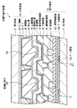
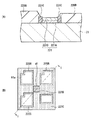
図1は、本開示の第1の実施の形態に係る有機EL表示装置(有機EL表示装置1)の断面構成を表すものである。有機EL表示装置1は、例えば、画素として複数の有機EL素子10Aが形成された素子基板10上に、封止層30を介して対向基板20が接着されたものであり、光を対向基板20の上方から取り出すトップエミッション型の有機EL表示装置である。この有機EL表示装置1では、例えば赤(R),緑(G),青(B),白(W)の4色のサブピクセルにより1つのピクセルが構成されている。
<First Embodiment>
[Constitution]
FIG. 1 illustrates a cross-sectional configuration of an organic EL display device (organic EL display device 1) according to the first embodiment of the present disclosure. In the organic
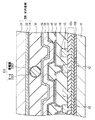
(素子基板10)
素子基板10では、表示領域(後述の表示領域110)を構成する画素として、有機EL素子10Aが、例えばマトリクス状に複数配置されている。例えば、素子基板10では、第1基板11上に、画素の駆動素子として、ゲート電極12a、ゲート絶縁膜12b、図示しないソース電極,ドレイン電極および半導体層を含むTFT12が画素毎に配設されている。このTFT12上には、層間絶縁膜12cを介して配線層13が設けられている。配線層13は、層間絶縁膜12cに設けられたコンタクトプラグを通じて、例えばTFT12のソース電極またはドレイン電極に電気的に接続されている。これらのTFT12および配線層13を含む画素回路は、層間絶縁膜14によって覆われている。素子基板10では、この層間絶縁膜14上に、表示領域(後述の表示領域110)を構成する画素としての有機EL素子10Aが複数配置されている。
(Element substrate 10)
In the
第1基板11は、例えばガラス基板あるいはプラスチック基板からなる。ガラス基板としては、例えば、高歪点ガラス、ソーダ石灰ガラス(Na2O・CaO・SiO2)、硼珪酸ガラス(Na2O・B2O3・SiO2)、フォルステライト(2MgO・SiO2)および鉛ガラス(Na2O・PbO・SiO2)などが挙げられる。あるいは、これらのガラスの表面に絶縁膜が形成されたものであってもよいし、他にも石英、シリコン、金属などの表面に絶縁膜が形成されたものを用いることもできる。プラスチック基板としては、例えば、ポリメチルメタクリレート(ポリメタクリル酸メチル,PMMA)、ポリビニルアルコール(PVA)、ポリビニルフェノール(PVP)、ポリエーテルスルホン(PES)、ポリイミド(PI)、ポリカーボネート(PC)あるいはポリエチレンテレフタレート(PET)などの有機ポリマーが挙げられる。尚、プラスチック基板は、可撓性を有するフィルム状あるいはシート状の形態のものも含む。
The
TFT12は、例えば後述の画素回路40におけるトランジスタ3A,3Bに相当するものであり、その構成は例えば逆スタガ構造(ボトムゲート構造)でもよいしスタガ構造(トップゲート構造)であってもよい。
The
層間絶縁膜12c,14は、酸化シリコン(SiO2)、BPSG、PSG、BSG、AsSG、PbSG、SiON、SOG(スピンオングラス)、低融点ガラス、ガラスペーストといったSiO2系無機材料、SiN系無機材料、およびポリイミド等の樹脂材料のうちのいずれかよりなる単層膜か、あるいはそれらのうちの2種以上よりなる積層膜である。
The
配線層13は、導電性金属よりなり、例えば下部電極15との接触面には、下部電極15に対する接触抵抗が小さな金属またはそのような金属酸化物を有することが望ましい。
The
層間絶縁膜14は、上記層間絶縁膜12と同様の材料により構成され、平坦性に優れた材料からなることが望ましい。
The
有機EL素子10Aは、例えば下部電極15、発光層を含む有機層17、抵抗層18および上部電極19がこの順に積層されたものである。下部電極15は、層間絶縁膜14に設けられたコンタクトホールを通じて、配線層13に電気的に接続されている。素子基板10では、複数の有機EL素子10Aはそれぞれ、層間絶縁膜14上に形成された画素間絶縁膜16によって素子分離されている。具体的には、画素間絶縁膜16には、下部電極15に対向して開口が形成されており、この開口において、上記のような下部電極15、有機層17、高抵抗層18および上部電極19の積層構造が形成されている。尚、上部電極19上には、更に保護層が形成されていてもよい。
In the
下部電極15は、有機EL素子10A毎に設けられている。下部電極15の構成材料としては、例えばアノードとして機能する場合には、例えば白金(Pt),金(Au),銀(Ag),クロム(Cr),タングステン(W),ニッケル(Ni),銅(Cu),鉄(Fe),コバルト(Co),タンタル(Ta)などの仕事関数の高い金属の単体あるいはそのような金属の合金が挙げられる。合金としては、例えば、銀を主成分とし、0.3重量%〜1重量%のパラジウム(Pd)と、0.3重量%〜1重量%の銅とを含むAg−Pd−Cu合金、あるいはAl−Nd合金を挙げることができる。あるいは、下部電極15は、上記のような金属元素の単体または合金よりなる金属膜と、ITO等の透明導電膜との積層構造を有していてもよい。下部電極15は、正孔注入性の高い材料により構成されていることが望ましいが、そうでない材料(アルミニウム(Al)あるいはアルミニウムを含む合金等)であっても、適切な正孔注入層を設けることによってアノードとして使用することができる。この下部電極15の厚みは、例えば10nm〜1000nmである。尚、ボトムエミッション型の場合には、透明導電膜、例えばインジウムとスズの酸化物(ITO)、インジウム亜鉛オキシド(IZO)、および酸化亜鉛(ZnO)とアルミニウム(Al)との合金のうちのいずれかよりなる単層膜または2種以上からなる積層膜により構成されている。
The
画素間絶縁膜16は、有機EL素子10Aの下部電極15と上部電極19との絶縁性を確保すると共に、それぞれの画素領域を区画(分離)するためのものである。画素間絶縁膜16は、平坦性に優れると共に、水分による有機層17の劣化を防止して発光輝度を維持するために吸水率の低い絶縁材料から構成することが望ましく、例えばポリイミド樹脂、アクリル樹脂あるいはノボラック樹脂等よりなる。この画素間絶縁膜16の開口配列に応じて、複数の有機EL素子10Aの配列は、例えばストライプ配列、ダイアゴナル配列、デルタ配列、あるいは、レクタングル配列とされる。
The inter-pixel
有機層17は、少なくとも有機電界発光層(以下、単に発光層という)を含み、本実施の形態では、この発光層(例えば、白色発光層)が全画素に共通の層として形成されている。これにより、画素毎の塗り分けプロセスを省いている。白色発光層としては、青色発光層および黄色発光層を積層したもの、あるいは、青色、緑色、赤色の発光層を積層したものなどが挙げられる。赤色発光層としては、例えば赤色発光材料,正孔輸送性材料および電子輸送性材料のうち少なくとも1種を含み、例えば4,4−ビス(2,2−ジフェニルビニン)ビフェニル(DPVBi)に2,6−ビス[(4'−メトキシジフェニルアミノ)スチリル]−1,5−ジシアノナフタレン(BSN)を混合したものから構成されている。緑色発光層は、例えば、緑色発光材料,正孔輸送性材料および電子輸送性材料のうち少なくとも1種を含み、例えば、ADNやDPVBiにクマリン6を混合したものから構成されている。青色発光層は、例えば、青色発光材料,正孔輸送性材料および電子輸送性材料のうち少なくとも1種を含み、例えば、DPVBiに4,4'−ビス[2−{4−(N,N−ジフェニルアミノ)フェニル}ビニル]ビフェニル(DPAVBi)を混合したものから構成されている。有機層17には、このような発光層の他にも、例えば、正孔注入層、正孔輸送層、電子輸送層などが積層されていてもよい。また、電子輸送層と上部電極19との間には、例えばリチウム(Li)、セシウム(Cs)、カルシウム(Ca)、バリウム(Ba)、インジウム(In)あるいはマグネシウム(Mg)等の酸化物または複合酸化物よりなる電子注入層が設けられていてもよい。更に、これらの積層構造をユニット(便宜上、タンデムユニットと呼ぶ)として、2つ以上のタンデムユニットが接続層を介して積層されていてもよい。
The
高抵抗層18は、有機層17と上部透明電極19の間において、透明かつ電気抵抗率の高い材料、例えば酸化ニオブ(Nb2O5)、ITOあるいはIZOにより構成されている。高抵抗層18を設けることにより、下部電極15および上部電極19間に電圧を印加したときに、例えば異物などに起因して、それらの電極間に短絡が発生することを抑制し、欠陥画素あるいは欠線の発生を防止することができる。この高抵抗層18の電気抵抗率は、例えば1×10⁶Ω・m〜1×10⁸Ω・mであることが望ましい。但し、高抵抗層18は、必要に応じて設けられればよく、有機層17上に直に上部電極19が形成されていてもよい。
The
上部電極19は、有機層17と高抵抗層18を介して電気的に接続され、複数の有機EL素子10Aに共通して設けられている。本実施の形態では、トップエミッション型であることから、この上部電極19は、透明導電膜よりなる。透明導電膜としては、例えばインジウムとスズの酸化物(ITO)、InZnO(インジウ亜鉛オキシド)、および酸化亜鉛(ZnO)とアルミニウム(Al)との合金のうちのいずれかよりなる単層膜または2種以上からなる積層膜である。この上部電極19の厚みは、例えば10nm〜500nmである。ここで、上記のような透明導電膜は高抵抗であるため、通常電圧降下を抑制するために、厚膜化してシート抵抗を下げる必要があり、これによって光学特性を損なうことがある。これに対し、本実施の形態では、後述するように、対向基板20に設けられる低抵抗層221Bにより電圧降下が抑制されることから、上部電極19を薄膜化して、良好な光学特性を得ることができる。
The
これらの高抵抗層18および上部電極19は、有機層17への水分到達を防止する保護膜としても機能するが、必要に応じて、更に、上部電極19上に、保護層(図示せず)を形成してもよい。この保護層は、絶縁性材料または導電性材料のいずれにより構成されていてもよい。絶縁性材料としては、無機アモルファス性の絶縁性材料、例えばアモルファスシリコン(a−Si),アモルファス炭化シリコン(a−SiC),アモルファス窒化シリコン(a−Si1-xNx)、アモルファスカーボン(a−C)等が好ましい。このような無機アモルファス性の絶縁性材料は、グレインを構成しないため透水性が低く、良好な保護膜となる。この保護層は、特に真空蒸着法のような成膜粒子のエネルギーが小さい成膜方法、あるいは、CVD(Chemical Vapor Deposition;化学気相成長)法を用いて形成されることが望ましい。下地に与える影響を小さくすることができるためである。また、有機層17の劣化を防止するために成膜温度を常温に設定し、保護層の剥がれを防止するために保護層のストレスが最小になる条件で成膜することが望ましい。更には、上部電極19を大気に暴露することなく形成することが望ましく、これにより大気中の水分や酸素による有機層17の劣化を防止できる。尚、このような絶縁材料からなる保護層を設ける場合には、上部電極19と、後述の低抵抗層221Bを電気的に接続するためにコンタクトホールを形成する必要がある。
The
(封止層30)
封止層30は、素子基板10を封止すると共に、素子基板10と対向基板20との接着層となるものであり、外部から有機層17への水分の侵入を防止する目的と、機械的な強度を増す目的で形成される。封止層30は、例えば紫外線(UV)硬化樹脂あるいは熱硬化樹脂等により構成され、本実施の形態では、絶縁性樹脂が用いられる。この封止層30は、基板外周部にダム材(外壁)として設けられた樹脂層310aと、この樹脂層310によって囲まれた領域内に形成された樹脂層310b(いずれも図1には図示せず)とを有している。尚、これらのうち、有機EL素子10Aに対向する樹脂層310bでは、有機層17から発光した光の透過率が80%以上であることが望ましい。一方、ダム材としての樹脂層310aについては、透過率については特に制限されないが、水分の透過率が低いことが重要である。図1では、封止層30として、これらのうち樹脂層310bの一部に対応する部分が示されている。
(Sealing layer 30)
The
封止層30の厚みは、例えば3〜20μmが好適である。20μm以下とすることにより、有機EL素子10Aと後述のカラーフィルタ層との間の距離を適切に保持し、表示面を斜めから見たときと正面から見たときの輝度変化や色度変化を抑制して、良好な視野角特性を得ることができる。また、3μm以上とすることにより、封止時に異物などが挟み込まれた場合であっても、その異物が有機EL素子10Aを加圧することに起因する滅点の発生を抑制することができる。
The thickness of the
尚、詳細は後述するが、この封止層30では、樹脂層310a,310b間に空隙を有しており(バッファ層を有しており)、この空隙部分に対向して、遮光パターン311が形成されている。また、本実施の形態のように、封止層30として絶縁性樹脂を用いる場合には、封止プロセスの際に充填する樹脂量は、封止体積に対して100〜120%とするのがよい。
Although details will be described later, this
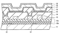
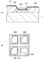
(対向基板20)
対向基板20は、第2基板21の一面(素子基板10側の面)に、カラーフィルタおよびブラックマトリクスを含むCF/BM層22が形成されたものである。このCF/BM層22には、所定の位置にピラー23が配設されており、これらのCF/BM層22およびピラー23を覆って導電膜24が形成されている。第2基板21は、上記第1基板11の構成材料として挙げたものと同様のものから構成され、第1基板11と同一の材料から構成されてもよいし、異なっていてもよいが、第2基板21は、透明性を有する材料よりなる。
(Opposing substrate 20)
The
図2は、対向基板20のピラー23付近の構成を拡大して示したものである。図3は、対向基板20を封止層30の側からみた構成(但し、導電膜24の図示は省略)である。尚、図2は、図3のI−I線における矢視断面図である。
FIG. 2 is an enlarged view of the configuration in the vicinity of the
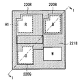
対向基板20の一面には、無機遮光層221Aおよび低抵抗層221B(導電層)を有する積層膜221が形成されている。積層膜221には、各有機EL素子10Aに対向して、無機遮光層221Aおよび低抵抗層221Bを貫通する開口部H1が設けられている。各開口部H1には、それぞれを埋め込むように、カラーフィルタを構成する赤色樹脂層220R、緑色樹脂層220Gおよび青色樹脂層220Bが形成されている。具体的には、本実施の形態では、上述したようにR,G,B,Wの4画素を1ピクセルとした構成であるため、例えば、2×2の配列で4画素が配置され、4つの開口部H1のいずれかに赤色樹脂層220R、緑色樹脂層220Gおよび青色樹脂層220Bが形成されている。尚、W画素については、カラーフィルタを設ける必要はないが、必要に応じて、輝度調整のための透過率制御フィルタが設けられていてもよい。
On one surface of the
赤色樹脂層220R,緑色樹脂層220G,青色樹脂層220B(以下、これらを総称してカラーフィルタ層という場合もある)はそれぞれ、積層膜221の開口部H1を埋め込むと共に、低抵抗層221Bの縁部e1にオーバーラップして形成されている。即ち、赤色樹脂層220R、緑色樹脂層220Gおよび青色樹脂層220Bの各端部e2は、積層膜221の縁部e1を覆うように形成されている。ピラー23は、それらの赤色樹脂層220R、緑色樹脂層220Gおよび青色樹脂層220Bから露出した低抵抗層221B上の選択的な領域(ここでは、4画素に囲まれる中央)に配設されている。これらの赤色樹脂層220R、緑色樹脂層220Gおよび青色樹脂層220Bと、低抵抗層221Bと、ピラー23とを覆って、導電膜24が形成されている。以下、この対向基板20の各部の構成について詳細に説明する。
Each of the
積層膜221は、1または複数の無機膜を積層したものであり、遮光性と導電性との両方を兼ね備えている。本実施の形態では、主に遮光性を発揮する層(無機遮光層221A)と、主に導電性を発揮する層(低抵抗層221B)とが積層されており、これらの無機遮光層221Aおよび低抵抗層221Bが、第2基板21上において互いに同一パターンで形成されている。即ち、ブラックマトリクスとしての遮光性と、上部電極19の補助電極としての機能を、複数の無機膜の積層構造により実現するようになっている。
The
無機遮光層221Aは、例えば無機多層膜からなり、光の干渉現象を利用して遮光性を確保するものである。無機遮光層221Aを構成する各無機膜の材料は、特に限定されず、導電性を有するものであってもよいし、絶縁性を有するものであってもよいが、例えば金属あるいはシリコン(Si)の単体、あるいはそれらの酸化物、窒化物および酸窒化物のうちのいずれかよりなる。各層の屈折率、吸収係数および膜厚等を適切に設定することにより、必要な遮光性が確保されていればよい。尚、遮光性および導電性の両方を兼ね備えた材料、例えばクロム(Cr)あるいはグラファイト(C)等を用いることもできるが、本実施の形態のように、遮光性と導電性の機能を分離して多層構造を形成することが、遮光性および低抵抗確保の点で望ましい。
The inorganic
このような無機遮光層221Aの一例としては、第2基板21の側から順に、SiN(65nm)/a−Si(アモルファスシリコン)(20nm)/Mo(50nm)の3層積層膜が挙げられる。この積層構造では、SiN層の膜厚は、上記膜厚(65nm)から+(プラス)8%〜−(マイナス)8%の範囲内であれば、またa−Si層の膜厚は、上記膜厚(20nm)から+12%〜−12%の範囲内であれば、同程度の遮光性を確保することができる。更に、SiN層の代わりに、より屈折率の高い無機膜を形成すれば、膜厚のマージンは向上する。あるいは、第2基板21の側から順に、MoOx(45nm)/Mo(10nm)/MoOx(40nm)/Mo(50nm)の4層積層膜とすることもできる。一方、これらのMo層およびMoOx層の膜厚はそれぞれ、+15%〜−15%の範囲内まで許容することができる。また、Moの代わりにMoNxを用いれば、より厚みを大きくすることができる。尚、括弧内は各層の膜厚を示している。これらの構造では、いずれも表面側(低抵抗層221B側)に、Mo層を有するが、このMo層の厚みが50nm以上であってもよい。また、Mo以外の別の金属を積層させてもよい。これにより、より遮光性および導電性を確保し易くなる。
As an example of such an inorganic
低抵抗層221Bは、上部電極19の補助電極として機能するものであり、即ち、上部電極19(透明導電膜)よりも電気抵抗率が低くなるような材料および膜厚により構成されている。本実施の形態では、この低抵抗層221Bが、無機遮光層221A上に積層されており、互いに同一のパターン形状(開口部H1を含むパターン形状)を有している。
The low-
この低抵抗層221Bは、例えば、下部電極15をアノード、上部電極19をカソードとした場合には、例えば画素部の周辺領域に設けられたカソードコンタクト部に接続されている。これにより、上部電極19側から取り出された電流は、低抵抗層221Bおよびカソードコンタクト部を介して素子基板10側の電源に戻ってくる。尚、カソードコンタクト部は、素子基板10側に形成してもよいし、対向基板20側に形成してもよい。但し、対向基板20側に形成した方が、取り出した電流をそのまま同じ基板20内のカソードコンタクト部に戻すことができ、素子基板10側へ戻す場合に比べて抵抗差が小さくなるため、好適である。尚、下部電極15をカソードとした場合であっても、同様に、画素部周辺部にアノードコンタクト部を形成することで電気的には等価になる。
For example, when the
低抵抗層221Bは、1または複数の無機膜を積層したものであり、例えばモリブデンよりも抵抗率の低い材料、例えばアルミニウム(Al),銀(Ag),金(Au),銅(Cu),クロム,亜鉛(Zn),鉄(Fe),タングステン(W)およびコバルト(Co)等のうちの少なくとも1種が用いられることが望ましい。但し、反応性の高い材料を用いる場合には、最表面に、モリブデンやチタン等によりなる層を形成するとよい。
The
低抵抗層221Bの厚みは、電圧降下を十分に抑えるために、有機EL表示装置の特性に応じて適宜設定されればよいが、100nm〜1000nm程度が好適である。導電特性を考慮すると100nm以上が好適であり、製膜プロセスの負荷を考慮すると、1000nm以下が好適である。
The thickness of the
このような低抵抗層221Bの一例としては、例えば、無機遮光層221Aの側から順に、Al(300nm)/Mo(50nm)の2層積層膜が挙げられる。この他にも、Mo(50nm)/Al(300nm)/Mo(50nm)の3層積層膜であってもよいし、Ag合金(300nm)の単層膜であってもよい。尚、無機遮光層221Aの一例として挙げた積層膜構造のうち表面側のMo層(50nm)は、遮光性と共に導電性も有するため、実際には、低抵抗層221Bの一部としても機能する。
As an example of such a
赤色樹脂層220R,緑色樹脂層220G,青色樹脂層220Bはそれぞれ、特定の波長域の光を選択的に透過する(他の波長の光は吸収する)カラーフィルタである。これにより、各画素では、有機層17から発せられた白色光を、R,G,Bのいずれかの色光として出射させることができる。但し、W画素(高輝度画素)では、有機層17から発せられた白色光を、カラーフィルタによって吸収させることなく、そのまま白色光として取り出す。このような赤色樹脂層220R,緑色樹脂層220G,青色樹脂層220Bは、例えば感光性樹脂に、染料あるいは顔料を混入したものである。また、各層の厚みは、必要とされる色度等に応じて適宜設定されればよいが、例えば0.1μm〜5μmである。
Each of the
ピラー23は、素子基板10および対向基板20間のスペーサとして機能すると共に、詳細は後述するが、積層膜221の低抵抗層221Bと、素子基板10の上部電極19とを電気的に接続するための部材である。このため、ピラー23は、導電性を有する材料から構成されることが望ましいが、本実施の形態のように、絶縁材料から構成されていてもよい。例えば、ピラー23は、フォトレジスト等の感光性樹脂を用いて形成され、その表面が導電膜24によって被覆されている。ここでは、ピラー23は、積層膜221上において、赤色樹脂層220R,緑色樹脂層220G,青色樹脂層220Bのいずれの層よりも十分に突出して形成されている。このピラー23と、これを覆う導電膜24とが、本開示における導電性部材の一具体例である。
The
このピラー23は、対向基板20の面内に複数配設される。このため、複数のピラー23の高さのばらつきを吸収し得る程度以上の弾性を有していることが望ましい。ピラー23の形成時に高さにばらつきが生じると、封止時に上部電極19と最初にコンタクトする部分(比較的高いピラー23)と、時間的に後からコンタクトする部分(比較的低いピラー23)が生じる。ピラー23が十分な弾性を有していれば、高さのあるピラー23を弾性変形により縮めてコンタクトさせることができ、低いピラー23の高さに合わせてセルギャップを規定することができる。ピラー23に高さのばらつきが生じた場合であっても、基板全面でのコンタクトが可能となる。まら、ピラー23が弾性を有することで、高さのばらつきに起因して生じるクラックの発生を抑制することもできる。
A plurality of
導電膜24は、例えばITO等の透明導電膜よりなり、厚みは例えば10nm〜5000nmである。尚、ここでは、導電膜24がピラー23の表面だけでなく、赤色樹脂層220R,緑色樹脂層220G,青色樹脂層220Bの表面をも覆っているので、導電膜24は透明性を有する必要があるが、必ずしも透明性を有している必要はない。即ち、低抵抗層221Bと上部電極19とがピラー23を介して電気的に接続されればよいので、ピラー23が絶縁性材料からなる場合、導電膜24は、ピラー23の表面と、低抵抗層221Bの表面の一部(例えばピラー23の周辺領域)とを少なくとも覆って形成されていればよい。このようにピラー23とその周辺の局所的な領域にのみ導電膜24を設けてもよい。この場合には、導電膜24が無機遮光層221A下に形成されることとなるので、導電膜24を、透明導電膜に限らず、他の金属材料、例えば、上記低抵抗層221Bと同様の材料を用いて形成可能である。
The
(上部電極19と低抵抗層221Bの電気的接続)
本実施の形態では、上記のように、第2基板上に、無機遮光層221Aおよび低抵抗層221Bの積層膜221を有し、この積層膜221の開口部H1に、赤色樹脂層220R,緑色樹脂層220G,青色樹脂層220Bが形成されている。積層膜221の低抵抗層221B上には、赤色樹脂層220R,緑色樹脂層220G,青色樹脂層220Bの各層から突出してピラー23が設けられ、これらのピラー23および低抵抗層221Bを含む第2基板21の全面が導電膜24により覆われている。ピラー23の先端部分では、導電膜24と、素子基板10の上部電極19とが接触している。これにより、ピラー23および導電膜24(導電性ピラー)を介して、上部電極19と低抵抗層221Bが電気的に接続されている。
(Electric connection between
In the present embodiment, as described above, the
このように、ピラー23を用いて上部電極19と低抵抗層221Bとの電気的接続を確保する場合、ピラー23を対向基板20側に予め形成しておくことから、接続位置を明確に規定することができる。
As described above, when the electrical connection between the
[製造方法]
上記のような有機EL表示装置1は、例えば次のようにして製造することができる。図4〜図12は、有機EL表示装置1の製造工程を表したものである。
[Production method]
The organic
(素子基板10の作製)
まず、素子基板10を作製する。具体的には、図4(A)に示したように、第1基板11上に、公知の薄膜形成プロセスにより、ゲート電極12a、ゲート絶縁膜12bおよび層間絶縁膜12c等を順次形成することにより、TFT12を形成した後、このTFT12に導通する配線層13を形成する。
(Preparation of element substrate 10)
First, the
続いて、図4(B)に示したように、層間絶縁膜14を形成する。具体的には、まず、基板全面にわたって、上述した材料よりなる層間絶縁膜14を、例えばCVD法、塗布法、スパッタリング法、あるいは各種印刷法等を用いて成膜する。この後、例えばフォトリソグラフィ法を用いたエッチングにより、層間絶縁膜14の配線層13に対向する領域にコンタクトホールH2を形成する。
Subsequently, as shown in FIG. 4B, an
次いで、図5(A)に示したように、下部電極15を形成する。即ち、まず、層間絶縁膜14上に、コンタクトホールH2を埋め込むように、上述した材料よりなる下部電極15を、例えばスパッタリング法等により成膜する。この後、成膜した下部電極15を、例えばフォトリソグラフィ法を用いたエッチングにより、所定の形状にパターニングすると共に画素毎に分離する。
Next, as shown in FIG. 5A, the
続いて、図5(B)に示したように、画素間絶縁膜16を形成する。即ち、まず、基板全面にわたって、上述した材料よりなる画素間絶縁膜16を成膜した後、下部電極15に対応する領域に開口部H3を形成する。この際、画素間絶縁膜16として感光性樹脂を用いる場合には、成膜後、フォトマスクを用いて露光することにより開口部H3を形成可能である。また、開口部H3の形成後、必要に応じてリフローを行ってもよい。この開口部H3がいわゆる各画素の発光領域(画素開口)となる。
Subsequently, as shown in FIG. 5B, an inter-pixel
次に、図6(A)に示したように、有機層17を形成する。本実施の形態では、上述したように、各画素に共通の発光層(例えば白色発光層)を形成することから、例えば赤色、緑色、青色の各発光材料を基板全面にわたって、例えば真空蒸着法により順次成膜する。あるいは、有機層17の形成方法としては、この真空蒸着法の他にも、スクリーン印刷法やインクジェット印刷法といった印刷法および塗布法を用いてもよい。また、転写用基板上に、レーザ光吸収層と有機層との積層体を形成しておき、この転写用基板にレーザ照射を行うことで転写用基板から有機層を分離して転写する、といったレーザ転写法を用いてもよい。尚、有機層17として、上記発光層の他に、正孔輸送層や電子輸送層等を形成する際には、いずれの層も発光層と真空一貫プロセスにより形成されることが望ましい。
Next, as shown in FIG. 6A, the
続いて、図6(B)に示したように、上述した材料よりなる高抵抗層18を、有機層17上の全面にわたって、例えばスパッタ法、蒸着法あるいはCVD法等により形成する。
Subsequently, as shown in FIG. 6B, the
次いで、図7に示したように、上述した透明導電膜よりなる上部電極19を、例えばスパッタ法により基板全面にわたって形成する。尚、上部電極19の形成後、例えば蒸着法やCVD法により、図示しない保護層を形成してもよい。このようにして、素子基板10を形成する。
Next, as shown in FIG. 7, the
(対向基板20の作製)
一方、対向基板20を、例えば次のようにして作製する。尚、図8〜図11は、対向基板20の作製工程を表すものであるが、各図において(A)は図2の構成に対応する断面拡大図、(B)は図3の構成に対応する平面模式図である。また、網掛け部分は、低抵抗層221B(積層膜221)の形成領域に対応する。
(Preparation of counter substrate 20)
On the other hand, the
具体的には、まず、図8(A),(B)に示したように、第2基板21上に積層膜221を成膜する。この際、まず、第2基板21上に、上述した積層構造、材料、膜厚等からなる無機遮光層221Aを、例えばスパッタ法あるいはCVD法等により成膜する。例えば、上述した積層膜構造例のうち、SiN/a−Si/Moの3層積層膜を形成する場合には、まず、SiN層およびa−Si層をこの順に、例えばCVD法により成膜した後、Mo層を例えばスパッタ法により成膜する。あるいは、MoOx/Mo/MoOx/Moの4層積層膜を形成する場合には、これらの各層を例えばスパッタ法により連続的に成膜すればよい。続いて、無機遮光層221A上に、上述した積層構造、材料、膜厚等からなる低抵抗層221Bを例えばスパッタ法により成膜する。このようにして、第2基板21の全面にわたって、無機遮光層221Aおよび低抵抗層221Bからなる積層膜221を成膜する。
Specifically, first, as illustrated in FIGS. 8A and 8B, a
この後、図9(A),(B)に示したように、積層膜221をパターニングする。具体的には、例えばフォトリソグラフィ法を用いたエッチングにより、積層膜221の選択的な領域を一括して除去することにより、複数の開口部H1を形成する。この際、例えば無機遮光層221Aとして、SiN/a−Si/Moの3層積層膜を形成する場合には、無機遮光層221Aおよび低抵抗層221Bをドライエッチングにより一括してパターニングすることができる。あるいは、MoOx/Mo/MoOx/Moの4層積層膜を形成する場合には、無機遮光層221Aおよび低抵抗層221Bをウェットエッチングにより一括してパターニングすることができる。
Thereafter, as shown in FIGS. 9A and 9B, the
次いで、図10(A),(B)に示したように、第2基板21上の積層膜221の開口部H1に、赤色樹脂層220R,緑色樹脂層220G,青色樹脂層220Bをそれぞれパターン形成する。
Next, as shown in FIGS. 10A and 10B, the
このように、本実施の形態では、ブラックマトリクスとして無機遮光層221Aと、上部電極19の補助電極としての低抵抗層21Bとを積層した後、この積層膜221を一括パターニングする。そして、このパターニング工程の後に、樹脂材料よりなるカラーフィルタ層を形成する。ここで、詳細は後述するが、カラーフィルタ層を構成する樹脂材料は、無機膜をパターニングする際に使用されるエッチング液に溶出し易いことから、カラーフィルタ層形成後に補助電極となるメタルのパターニングを行うと、カラーフィルタ層が損傷する虞がある。本実施の形態では、上述のように、ブラックマトリクスを無機遮光膜221Aにより形成すると共に、カラーフィルタ層形成前に、低抵抗層221Bをパターニングすることから、カラーフィルタ層の溶出を防止することができる。
Thus, in this embodiment, after laminating the inorganic
上記のように、カラーフィルタ層を積層膜221のパターニング後に、形成することから、カラーフィルタ層(赤色樹脂層220R,緑色樹脂層220G,青色樹脂層220B)は、低抵抗層221Bの縁部にオーバーラップして形成される。
As described above, the color filter layer (the
次いで、図11(A),(B)に示したように、低抵抗層221B上の選択的な領域に、ピラー23を形成する。ピラー23としては、例えばフォトスペーサ等に用いられる感光性アクリル樹脂を使用することができ、このような感光性樹脂をフォトマスクを用いて露光することにより形成する。この後、例えば基板全面にわたって、例えばスパッタ法により、上述した材料よりなる導電膜24を成膜することにより、対向基板20が形成される。
Next, as shown in FIGS. 11A and 11B,
(貼り合わせ(封止)工程)
次に、上記のようにしてそれぞれ作製した素子基板10および対向基板20を、封止層30を介して貼り合わせる。この際、例えば、ODF(One Drop Fill)法と呼ばれる成膜手法を用いるのが好ましい。ODF法とは、素子基板10(あるいは対向基板20)上に、複数の樹脂滴(樹脂ドロップ)を等間隔に配置し、真空中で両基板を圧着させる手法である。この後、大気に開放することで、基板にかかる圧力(大気圧)により樹脂滴が基板間に充填される。このようにして樹脂を充填した後、樹脂を硬化させる。
(Lamination (sealing) process)
Next, the
具体的には、まず、図12(A)に示したように、真空チャンバー内のプレート280A,280B間に素子基板10および対向基板20を対向配置させ、例えば素子基板10上に、封止層30として、樹脂層310a(ダム材)を素子基板10aの外周に沿って塗布した後、樹脂層310aによって囲まれた領域内に、樹脂層310bを、例えば樹脂材料を等間隔で複数個所に滴下する。ここで、樹脂層310a,310bは、硬化前の状態では、液体またはゲル状であるが、樹脂層310aは比較的粘性が高い材料からなり、樹脂層310bは、粘性の低い材料からなる。
Specifically, first, as shown in FIG. 12A, the
続いて、図12(B)に示したように、プレート280A,280Bを用いて、機械的に素子基板10および対向基板20を圧着する。これにより、素子基板10および対向基板20間の領域では、樹脂層310aによって囲まれる領域内において、樹脂層310bが広がる。
Subsequently, as shown in FIG. 12B, the
この後、図12(C)に示したように、素子基板10および対向基板20をチャンバー内から取り出し、大気に曝すと、大気圧によって素子基板10および対向基板20へ更に圧力がかかり、基板間が樹脂層310a,310bにより満たされる。最後に、樹脂層310a,310bを硬化させることにより、封止層30を形成する。以上により、図1に示した有機EL表示装置1を完成する。
Thereafter, as shown in FIG. 12C, when the
尚、樹脂層310a,310bとしては、熱硬化樹脂を用いても、光硬化樹脂を用いてもよいが、光硬化樹脂の場合にはカラーフィルタ層を透過する波長により硬化するものを用いる。または、光遅延型硬化樹脂を用いてもよく、この場合には、圧着前に予め光照射を行い、樹脂が完全に硬化する前に上記のようにして基板間に樹脂を充填させ、この後、再度光照射を行って樹脂を完全に硬化させる。
In addition, as the
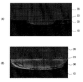
また、本実施の形態では、封止層30が導電性を有していないが、この場合、樹脂層310a,310bの塗布量(滴下量)としては封止体積(素子基板10および対向基板20間において必要な封止層30の体積)に対して120%以下であることが望ましく、100〜120%であることがより望ましい。但し、「封止体積」とは、素子基板10と対向基板20との間の領域のうちの有効画素領域に対応する体積に対応するものとする。例えば、この封止体積には、後述する遮光パターン311によって遮光される領域(樹脂バッファ層としての空隙310c)は含まれないものとする。封止樹脂が少なすぎると(例えば90%未満であると)、基板間の導通は確保できるものの、基板間に無視できない空隙が生じてしまい、封止むらとして視認されることが実験的にわかっている。一方、塗布量が多すぎると(例えば120%より大きいと)、基板間の導通を確保しにくいこともわかっている。例えば、120%では導通はとれるものの、不十分であり、135%になると導通をとることができなかった。これに対し、塗布量を105%とした場合には、視認されるような空隙も生じず、また基板間の導通も確保することができた。図13(A),(B)に塗布量が120%より大きい場合(135%)、図14(A),(B)に、塗布量が100〜120%の範囲内(105%)にある場合の基板界面付近の写真を示す。図13(A),(B)の例では、ピラー23が素子基板10と接触しておらず、図14(A),(B)の例では、ピラー23と素子基板10とが接触していることがわかる。
In this embodiment, the
但し、封止層30では、その外周部に樹脂層310a,310bのバッファ層として、図15(A),(B)に示したように、樹脂層310aと最も外側の樹脂層310bとの間に、空隙310cを設けてもよい。画素部と異なり、外周部では空隙が生じても視認性に影響を与えないので、特に問題はない。上述したようなODFプロセスにおいては、最終的に大気圧によって樹脂が押し出されると共に、ピラー23等の電気的接続部材の高さに応じてセルギャップ(封止層30の厚み)が規定される。このとき、余剰の樹脂は全て外側に押し出されることとなるが、外周部に、上記のような空隙310cを予め設けておくことにより、この空隙310cにおいて余剰樹脂を吸収することができ、画素部における封止層30を所望の厚みに制御し易くなる。よって、封止むらを効果的に低減することができる。また、図15(C),(D)に示したように、この空隙310cが設けられる部分を遮光パターン311で覆ってもよい。これにより、貼り合わせ後において、空隙310cの全域を埋めることなく、その一部(空隙310c1)が残ったとしても、この残存したが空隙310c1が視認されることを防止できる。尚、図15の各図において、(A),(C)図は圧着前(樹脂滴下直後)の平面構成、(B),(D)図は大気圧圧着後の平面構成をそれぞれ表している。
However, in the
[作用・効果]
有機EL表示装置1では、各画素では、図示しない駆動回路から供給される走査信号等に応じ、画素(有機EL素子10A)毎に、下部電極15および上部電極19を通じて有機層17に所定の駆動電流が注入される。これにより、有機層17の発光層では、正孔と電子との再結合により発光が生じる。有機層17から生じた光(白色光)は、高抵抗層18、上部電極19,封止層30および対向基板20を透過することにより、表示光として取り出される。対向基板20を通過する際、画素毎に対応する色のカラーフィルタ層(W画素では開口部H1)をそれぞれ透過することにより、R,G,B,Wのいずれかの色光として取り出される。
[Action / Effect]
In the organic
このように、トップエミッション型の有機EL表示装置1では、対向基板20の側にカラーフィルタ層が形成され、有機層17から発せられた白色光を上部電極19側から取り出し、カラーフィルタ層を透過させることによって、カラーの表示を実現する。このため、上部電極19としては、高抵抗な透明導電膜を用いる必要があるが、光学的な観点から上部電極19を厚膜化しにくい。上部電極19を薄膜化するとその分抵抗が高くなり、電圧降下が生じる。また、上述したように、大型化、高精細化に伴って、画素部内の領域毎の配線抵抗のばらつきが無視できなくなり、電圧降下に起因する面内輝度のばらつきが生じる。
Thus, in the top emission type organic
(比較例)
そこで、例えば、対向基板側に、低抵抗なメタルよりなる補助電極を形成することが考えられる。この場合、対向基板には、樹脂材料よりなるブラックマトリクス(以下、樹脂BMという)およびカラーフィルタ層が形成され、補助電極は、ブラックマトリクス上にパターン形成される。この補助電極と上部電極とを電気的に接続することで、電圧降下を抑制することができる。しかしながら、このように、樹脂BM上に補助電極を形成する場合、補助電極のパターニングの際に、フォトリソグラフィ法を用いてエッチングを行うことから、その過程において、強力なエッチャー剤によって樹脂が溶出してしまう。これにより、樹脂BMの反射率抑制効果が阻害され、表示不良を招くばかりか、エッチャー剤に溶出した樹脂を除去する必要があり、大型化、大量生産には不向きである。加えて、補助電極は、上記樹脂BMからはみ出すとその高反射率によって表示不良となることから、位置合わせのマージンを確保するために補助電極を樹脂BMよりも一回り小さくする必要がある。このため、特に画素の高精細化に伴って、補助電極の線幅が非常に狭くなり、精度良く補助電極を形成することが困難であると共に、十分な抵抗低減効果を得ることが難しい。
(Comparative example)
Therefore, for example, it is conceivable to form an auxiliary electrode made of a low-resistance metal on the counter substrate side. In this case, a black matrix (hereinafter referred to as a resin BM) and a color filter layer made of a resin material are formed on the counter substrate, and the auxiliary electrode is patterned on the black matrix. A voltage drop can be suppressed by electrically connecting the auxiliary electrode and the upper electrode. However, when the auxiliary electrode is formed on the resin BM in this way, since the etching is performed using the photolithography method when the auxiliary electrode is patterned, the resin is eluted by a strong etchant in the process. End up. As a result, the reflectance suppressing effect of the resin BM is hindered, leading to display failure, and it is necessary to remove the resin eluted in the etchant, which is unsuitable for large size and mass production. In addition, when the auxiliary electrode protrudes from the resin BM, display failure occurs due to its high reflectance. Therefore, it is necessary to make the auxiliary electrode slightly smaller than the resin BM in order to ensure a margin for alignment. For this reason, the line width of the auxiliary electrode becomes very narrow especially with higher definition of pixels, and it is difficult to form the auxiliary electrode with high accuracy, and it is difficult to obtain a sufficient resistance reduction effect.
これに対し、本実施の形態では、対向基板20側に、上部電極19に電気的に接続される低抵抗層221Bを形成することにより、上部電極19の電圧降下およびこれに起因する面内輝度ばらつきを抑制する。特に、本実施の形態では、対向基板20において、ブラックマトリクスとして無機遮光層221Aを設け、かつこの無機遮光層221A上に補助電極としての低抵抗層221Bを有する積層膜221を有している。製造プロセスにおいて、低抵抗層221Bと無機遮光層221Aとを同時に一括してパターニングすることができる。そして、このパターニング工程の後に、樹脂材料よりなるカラーフィルタ層(赤色樹脂層220R,緑色樹脂層220G,青色樹脂層220B)を形成する。本実施の形態では、上述のように、ブラックマトリクスを無機遮光膜221Aにより形成すると共に、カラーフィルタ層形成前に、低抵抗層221Bをパターニングすることから、樹脂材料の溶出を防止することができる。このように、本実施の形態では、カラーフィルタ層を備えた対向基板20において、カラーフィルタ層の溶出を防ぎ、かつ無機遮光層221Aおよび低抵抗層221Bを精度良くパターン形成することができる。
On the other hand, in the present embodiment, the
また、例えば、無機遮光膜211Aを、上述したような3層積層膜あるいは4層積層膜とすることで、一般的な樹脂BMと同等以上の遮光性能を実現できる。図16に、3層積層膜(SiN(65nm)/a−Si(20nm)/Mo(50nm))からなる無機遮光層211Aの反射率を実施例1−1として示す。また、4層積層膜(MoOx(45nm)/Mo(10nm)/MoOx(40nm)/Mo(50nm))からなる無機遮光層211Aの反射率を実施例1−2として示す。また、図16には、これらの実施例1−1,1−2の比較例として、樹脂BMの反射率を比較例1、酸化チタン(TiO2)単層膜を用いた場合の反射率を比較例2として示す。このように、実施例1−1,1−2のいずれにおいても、樹脂BMと同等以下の反射率となっており、特に実施例1−2では、広範囲の波長域にわたって反射率が低く、光学的に優れていることがわかる。 Further, for example, by using the inorganic light shielding film 211A as a three-layer laminated film or a four-layer laminated film as described above, a light shielding performance equal to or higher than that of a general resin BM can be realized. FIG. 16 shows the reflectance of the inorganic light-shielding layer 211A made of a three-layer laminated film (SiN (65 nm) / a-Si (20 nm) / Mo (50 nm)) as Example 1-1. Further, the reflectance of the inorganic light-shielding layer 211A composed of a four-layer laminated film (MoO x (45 nm) / Mo (10 nm) / MoO x (40 nm) / Mo (50 nm)) is shown as Example 1-2. Further, in FIG. 16, as a comparative example of Examples 1-1 and 1-2, the reflectance of the resin BM is shown as Comparative Example 1, and the reflectance when a titanium oxide (TiO 2 ) single layer film is used. This is shown as Comparative Example 2. As described above, in each of Examples 1-1 and 1-2, the reflectance is equal to or lower than that of the resin BM. In Example 1-2, the reflectance is low over a wide wavelength range. It turns out that it is excellent.
更に、本実施の形態では、無機遮光層221Aと低抵抗層221Bとを一括してパターニングできることから、補助電極としてのメタルをブラックマトリクス形成後に別途形成する場合に比べ、位置合わせのマージンを考慮する必要がない。換言すると、低抵抗層221Bは、無機遮光層221A下にそれと同一のパターンで形成されることとなる。このため、低抵抗層221Bの線幅を最大限に確保することが可能であり、上部電極19における電圧降下を効果的に抑制できる。
Furthermore, in this embodiment, since the inorganic light-
以上のように本実施の形態では、対向基板20側に無機遮光層221Aを設けると共に、この無機遮光層221A上に、上部電極19に電気的に接続された低抵抗層221Bが積層される。これにより、素子基板10の上部電極19が高抵抗な場合にも、それに起因する電圧降下を抑制できる。よって、大型化あるいは高精細化に伴って生じる発光輝度むらを低減し、表示品位を向上させることが可能となる。
As described above, in the present embodiment, the inorganic
続いて、上記第1の実施の形態の変形例(変形例1)について説明する。尚、上記実施の形態における構成要素と同一のものには同一の符号を付し、適宜説明を省略する。 Subsequently, a modified example (modified example 1) of the first embodiment will be described. In addition, the same code | symbol is attached | subjected to the same thing as the component in the said embodiment, and description is abbreviate | omitted suitably.
<変形例1>
図17および図18は、変形例1に係る対向基板(対向基板20A)の構成を表したものである。図17は、対向基板20Aのピラー23付近の構成を拡大して示したものである。図18は、対向基板20Aを封止層30の側からみた構成(但し、導電膜24の図示は省略)である。尚、図17は、図18のI−I線における矢視断面図である。
<
17 and 18 show the configuration of the counter substrate (counter
対向基板20Aは、上記第1の実施の形態の対向基板20と同様、素子基板10上に封止層30を介して貼り合わせられるものであり、第2基板21の一面(素子基板10側の面)に、カラーフィルタ層と、ブラックマトリクスおよび補助電極としての積層膜221とが形成されたものである。また、この積層膜221上の所定の位置にピラー23が配設され、これらのカラーフィルタ層、低抵抗層221Bおよびピラー23を覆って導電膜24が形成されている。
Similar to the
但し、本変形例では、積層膜221の開口部H1の内壁を覆って、更に樹脂遮光層221cが設けられている。この樹脂遮光層221cによって形成される開口部H1aを埋め込むようにカラーフィルタ層が形成されている(カラーフィルタ層が開口部H1aの縁部にオーバーラップして形成されている)。
However, in this modification, a resin light shielding layer 221c is further provided so as to cover the inner wall of the opening H1 of the
樹脂遮光層221cは、開口部H1の内壁を覆うと共に、開口部H1に非対向の領域では、例えば積層膜221(低抵抗層221B)の上面を覆って形成されている。但し、ピラー23が配設されている箇所の周辺の少なくとも一部(d1)は、低抵抗層221Bが樹脂遮光層221cから露出している。導電膜24を介して上部電極19と低抵抗層221Bとを電気的に接続させるためである。この樹脂遮光層221cは、例えば感光性樹脂に、黒色の顔料等を混入したものである。あるいは、樹脂遮光層221cとしては、グラファイト等の導電性を有する材料を用いてもよい。遮光性に加え、導電性がより向上する。
The resin light shielding layer 221c covers the inner wall of the opening H1, and is formed, for example, so as to cover the upper surface of the laminated film 221 (
上記のような対向基板20Aは、例えば次のようにして作製することができる。図19〜図21は、対向基板20Aの作製工程を表すものであるが、各図において(A)は図17の構成に対応する断面拡大図、(B)は図18の構成に対応する平面模式図である。また、網掛け部分は、低抵抗層221B(積層膜221)および樹脂遮光層221cの各形成領域に対応する。
The
具体的には、まず、図19(A),(B)に示したように、上記第1の実施の形態と同様にして、第2基板21上に、無機遮光層221Aおよび低抵抗層221Bを順に成膜した後、一括してパターニングすることにより、開口部H1を有する積層膜221を形成する。
Specifically, first, as shown in FIGS. 19A and 19B, the inorganic
次いで、図20(A),(B)に示したように、積層膜221の開口部H1の内壁を覆うと共に、積層膜221の上面を覆って、樹脂遮光層221cを成膜する。この後、例えばリソグラフィ技術により、樹脂遮光層221cの一部d1(ピラー形成予定領域)を開口し、低抵抗層221Bを露出させる。
Next, as shown in FIGS. 20A and 20B, a resin light-shielding layer 221c is formed to cover the inner wall of the opening H1 of the
続いて、図21(A),(B)に示したように、第2基板21上の開口部H1aに、赤色樹脂層220R,緑色樹脂層220G,青色樹脂層220Bをそれぞれパターン形成する。最後に、低抵抗層221B上の選択的な領域に、上記第1の実施の形態と同様にして、ピラー23および導電膜24を成膜することにより、対向基板20Aを作製することができる。
Subsequently, as shown in FIGS. 21A and 21B, the
このように、本変形例においても、ブラックマトリクスとして無機遮光層221Aと、上部電極19の補助電極としての低抵抗層221Bとを積層した後、この積層膜221を一括パターニングする。そして、このパターニング工程の後に、樹脂材料よりなる樹脂遮光層221cおよびカラーフィルタ層を形成する。従って、本変形例においても、カラーフィルタ層形成前に、低抵抗層221Bをパターニングすることから、カラーフィルタ層の溶出を防止することができる。よって、上記第1の実施の形態と同等の効果を得ることができる。
Thus, also in this modification, after laminating the inorganic
また、無機遮光層221Aでは、光の干渉現象を利用するために、入射光の波長および角度、あるいは膜厚の設計値からのずれ等によって、外光あるいは内部反射光の遮光性が不十分となる場合もある。そこで、本変形例のように、積層膜221の側面部に、樹脂遮光層221cを設けることにより、特に、斜め方向から入射する光の遮光性を確保することができる。これにより、内部反射を抑制してより表示品位を向上させることができる。
In addition, since the inorganic
尚、上記変形例では、積層膜221の開口部H1の内壁を覆って、樹脂遮光層221cを形成したが、樹脂層ではなく金属層を更に積層させた構成としてもよい。例えば、図17において、積層膜221を挟むように、樹脂遮光層221cの代わりに、MoOx(45nm)/Mo(10nm)/MoOx(40nm)の3層積層膜を形成してもよい。このような構造とすれば、遮光性および導電性が補強され、内部反射を防ぐと共に、低抵抗層221Bと上部電極19との導通も確保し易くなる。
In the above modification, the resin light shielding layer 221c is formed so as to cover the inner wall of the opening H1 of the
<第2の実施の形態>
図22および図23は、本開示の第2の実施の形態に係る対向基板(対向基板20B)の構成を表したものである。図22は、対向基板20Bのピラー23付近の構成を拡大して示したものである。図23は、対向基板20Bを封止層30の側からみた構成(但し、オーバーコート層222および導電膜24の図示は省略)である。尚、図22は、図23のI−I線における矢視断面図である。
<Second Embodiment>
22 and 23 show the configuration of the counter substrate (
対向基板20Bは、上記第1の実施の形態の対向基板20と同様、素子基板10上に封止層30を介して貼り合わせられるものであり、第2基板21の一面(素子基板10側の面)に、カラーフィルタ層が形成されたものである。また、この対向基板20Bには、上部電極19の補助電極としての低抵抗層(低抵抗層221E)がパターン形成されており、この低抵抗層221E上にピラー23が配設されている。これらのカラーフィルタ層、低抵抗層221Eおよびピラー23を覆って導電膜24が形成されている。
Similar to the
但し、本実施の形態では、ブラックマトリクスとして、樹脂遮光層221Dが設けられている。カラーフィルタ層(赤色樹脂層220R,緑色樹脂層220G,青色樹脂層220B)は、この樹脂遮光層221Dの開口部H3に形成されている。これらの樹脂遮光層221Dおよびカラーフィルタ層を覆うように、第2基板21の全面にわたってオーバーコート層222(保護層)が形成されている。このオーバーコート層222上の選択的な領域(樹脂遮光層221Dに重畳する領域)に、低抵抗層221Eが形成されている。
However, in this embodiment, the resin light-
樹脂遮光層221Dは、上記変形例1の樹脂遮光層221cと同様、例えば感光性樹脂に遮光性を有する顔料を混入させたものからなる。オーバーコート層222は、カラーフィルタ層を保護する機能を有し、例えばアクリル樹脂、ITOあるいはIZOよりなる。低抵抗層221Eは、上記第1の実施の形態の低抵抗層221Bと同様、1または複数の無機膜を積層したものであり、上記低抵抗層221Bと同様の構成材料を用いることができる。また、この低抵抗層221Eの平面形状は、樹脂遮光層221Dの形状に沿って格子状となる。
The resin
上記のような対向基板20Bは、例えば次のようにして作製することができる。図24〜図26は、対向基板20Bの作製工程を表すものであるが、各図において(A)は図22の構成に対応する断面拡大図、(B)は図23の構成に対応する平面模式図である。また、網掛け部分は、樹脂遮光層221Dの形成領域に対応する。
The
具体的には、まず、図24(A),(B)に示したように、第2基板21上に、樹脂遮光層221Dおよびカラーフィルタ層をそれぞれパターン形成する。次いで、図25(A),(B)に示したように、遮光層221Dおよびカラーフィルタ層を覆って、オーバーコート層222を例えばスリットコータ法、スパッタ法により形成する。
Specifically, first, as shown in FIGS. 24A and 24B, a resin
続いて、図26(A),(B)に示したように、オーバーコート層222上に、上述した低抵抗材料を、例えばスパッタ法により成膜した後、例えばフォトリソグラフィ法を用いたエッチングによりパターニングすることにより、低抵抗層221Eを形成する。最後に、低抵抗層221E上の選択的な領域に、上記第1の実施の形態と同様にして、ピラー23を形成し、更に導電膜24を成膜することにより、対向基板20Bを作製することができる。
Subsequently, as shown in FIGS. 26A and 26B, the above-described low-resistance material is formed on the
このように、本実施の形態では、ブラックマトリクスとして樹脂遮光層221Dと、カラーフィルタ層を形成した後、低抵抗層221Eを形成する前に、オーバーコート層222を形成することで、低抵抗層221Eのパターニング時に使用するエッチング液からカラーフィルタ層および樹脂遮光層221Dが保護され、これらの損傷を抑制できる。従って、本実施の形態においても、低抵抗層221Eの形成工程において、カラーフィルタ層の溶出を防止することができる。よって、上記第1の実施の形態と同等の効果を得ることができる。
As described above, in this embodiment, after forming the resin light-
また、樹脂材料からなるカラーフィルタ層や樹脂遮光層221Dは、水分あるいはガスの発生源となることから、これらの水分等が有機層17へ到達すると、有機層17の劣化を生じさせる。本実施の形態のように、オーバーコート層222を設けることで、このようなカラーフィルタ層や樹脂遮光層221Dからの水分等の有機層17への侵入を遮断し、有機EL表示装置の信頼性を向上させることができる。
Further, since the color filter layer made of a resin material and the resin
次に、上記第1および第2の実施の形態の変形例(変形例2〜5)について説明する。変形例2,3は、ピラーの他の構成に関するものであり、変形例4,5は、上部電極と低抵抗層との電気的接続手段の他の手法に関するものである。変形例2,3では、上記第1の実施の形態の積層膜221を用いた構成を例に挙げて説明するが、第2の実施の形態にも同様に適用可能である。尚、上記第1実施の形態における構成要素と同一のものには同一の符号を付し、適宜説明を省略する。
Next, modified examples (modified examples 2 to 5) of the first and second embodiments will be described.
<変形例2>
図27および図28は、変形例2に係る対向基板(対向基板20C)の構成を表したものである。図27は、対向基板20Cのピラー(ピラー23A)付近の構成を拡大して示したものである。図28は、対向基板20Cを封止層30の側からみた構成(但し、導電膜24の図示は省略)である。尚、図27は、図28のI−I線における矢視断面図である。
<
27 and 28 show the configuration of the counter substrate (counter substrate 20C) according to the second modification. FIG. 27 is an enlarged view of the configuration near the pillar (
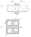
対向基板20Cは、上記第1の実施の形態の対向基板20と同様、素子基板10上に封止層30を介して貼り合わせられるものである。また、対向基板20Cは、第2基板21の一面(素子基板10側の面)に、カラーフィルタ層(赤色樹脂層220R,緑色樹脂層220G,青色樹脂層220B)と、ブラックマトリクスおよび補助電極としての積層膜221とが形成されたものである。この積層膜221上の所定の位置には、ピラー23Aが配設され、これらのカラーフィルタ層、低抵抗層221Bおよびピラー23Aを覆って導電膜24が形成されている。
The counter substrate 20C is bonded to the
但し、本変形例では、カラーフィルタ層のうちの選択的な1または複数の層が開口部H1の対向領域だけでなく、ピラー23Aに対向する積層膜221上の領域にも積層されている。即ち、ピラー23Aは、積層膜221上にカラーフィルタ層を介して配設されている。ここでは、青色樹脂層220Bおよび赤色樹脂層220Rが、ピラー23Aの対向領域まで延在形成され、積層膜221とピラー23Aとの間に、青色樹脂層220Bおよび赤色樹脂層220Rが積層されている。ピラー23Aは、上記第1の実施の形態のピラー23と同様、導電性材料または絶縁材料により構成され、例えばフォトスペーサ等に用いられる感光性樹脂により構成される。
However, in this modification, one or more selective layers of the color filter layers are stacked not only in the region facing the opening H1 but also in the region on the
このように、積層膜221上のピラー23Aに対向する領域までカラーフィルタ層を延在形成することにより、ピラー23Aの土台(本開示のフィルタ積層部に相当)を形成してもよい。これは特に、ピラー23Aの高さを十分にとることができない場合に、有効である。ピラー23Aと積層膜221との間に形成されたカラーフィルタ層の合計の厚みと、ピラー23Aの高さが、装置全体のセルギャップとなる。例えば、既存のフォトスペーサで使用されている材料等を用いた場合、ピラー23Aの高さが例えば3μm〜10μm程度となり、カラーフィルタ層から突出して、所望のセルギャップを確保することが困難である場合もある。このような場合、カラーフィルタ層を例えば1〜4μm程度の厚みで積層することにより、ピラー23Aを嵩上げして、所望のセルギャップを確保することができる。尚、カラーフィルタ層は、開口部H1からピラー23Aの対向領域まで延在して(繋げて)形成してもよいし、開口部H1付近とピラー3A付近とにおいて分離して形成してもよい(ピラー23Aの対向領域およびその周辺領域にだけ局所的にカラーフィルタ層が積層されていてもよい)。
As described above, the base of the
<変形例3>
図29および図30は、変形例3に係る対向基板(対向基板20D)の構成を表したものである。図29は、対向基板20Dのピラー(ピラー23B)付近の構成を拡大して示したものである。図30は、対向基板20Dを封止層30の側からみた構成(但し、導電膜24の図示は省略)である。尚、図29は、図30のI−I線における矢視断面図である。
<Modification 3>
FIGS. 29 and 30 show the configuration of the counter substrate (counter substrate 20D) according to the third modification. FIG. 29 is an enlarged view of the configuration in the vicinity of the pillar (
上記変形例2では、カラーフィルタ層をピラー23Aの土台として積層させたが、本変形例のように、カラーフィルタ層そのものをピラー(ピラー23B)として利用してもよい。例えば、緑色樹脂層220Gおよび赤色樹脂層220Rを、積層膜221上の所定の領域まで延在形成するか、あるいは局所的にカラーフィルタ層を積層させることにより、所望の高さのピラー23Bを形成可能である。このように積層膜221上の局所的な領域にカラーフィルタ層を積層させることにより、ピラー23Bを形成してもよく、上記第1の実施の形態と同様に、このピラー23Bを形成後に、基板全面にわたって導電膜24を成膜することで、ピラー23Bに対応する箇所で上部電極19の電気的接続を確保することができる。
In the second modification, the color filter layer is stacked as a base of the
<変形例4>
図31は、変形例4に係る有機EL表示装置の断面構成を表すものである。上記第1の実施の形態等では、上部電極19と低抵抗層221Bとの電気的接続を、ピラー23(詳細にはピラー23および導電膜24)を用いて行ったが、これらの電気的接続手段としては、他の手法を用いてもよい。
<Modification 4>
FIG. 31 illustrates a cross-sectional configuration of an organic EL display device according to Modification 4. In the first embodiment and the like, the electrical connection between the
例えば、本変形例のように、素子基板10および対向基板20E間に、導電性ボール23Cを介在させて、コンタクトをとる手法もある。この場合、対向基板20E側には、上記のようなピラー23を設けず、CF/BM層22の表面全体を導電膜24が覆うような構成となる。図32は、対向基板20Eの一部を拡大して表したものである。図33は、対向基板20Eを封止層30の側からみた構成(但し、導電膜24の図示は省略)である。尚、図32は、図33のI−I線における矢視断面図である。このように、対向基板20Eでは、第2基板21上において、積層膜221の開口部H1にカラーフィルタ層が形成され、導電膜24は、例えば、カラーフィルタ層および低抵抗層221Bの表面を覆って形成されている。
For example, as in this modification, there is a method of making a contact by interposing a conductive ball 23C between the
導電性ボール23Cは、素子基板10および対向基板20E間のスペーサとして機能し、その粒径(例えば直径が3〜20μm)によりセルギャップを規定するものである。この導電性ボール23Cは、特に低抵抗層221Bの直下に配置されなくともよく、基板貼り合わせの際に、素子基板10あるいは対向基板20上に散布されることにより配置される。このような導電性ボールとしては、例えばアクリル樹脂からなるボール23c1の表面を、導電膜23c2によりコーティングしたものが挙げられる。導電膜23c2としては、例えば金、チタンあるいは銀等の金属か、あるいはITO,IZO等の透明性導電膜を用いることができる。透明性導電膜を用いることにより、導電性ボール23Cが積層膜221の直下に配置されなかった場合でも、視認性に影響を及ぼしにくい。
The conductive ball 23C functions as a spacer between the
<変形例5>
図34は、変形例5に係る有機EL表示装置の断面構成を表すものである。上部電極19と低抵抗層221Bとの電気的接続手法としては、他にも、本変形例のように、素子基板10および対向基板20Eを、導電性を有する封止層(封止層30A)を介して貼り合わせる手法もある。
<Modification 5>
FIG. 34 illustrates a cross-sectional configuration of an organic EL display device according to Modification 5. As another electrical connection method between the
封止層30Aは、導電性を有する樹脂(例えばアクリル樹脂)に導電体材料を混ぜたものよりなる。導電体材料としては、金属ナノ材料、ナノサイズのカーボン、導電性ポリマー等が挙げられる。この封止層30Aの電気抵抗率は、特に限定されないが、例えば1×10⁶Ω・m〜1×10⁸Ω・mの範囲内であると、高抵抗層18としての機能を兼ねることができる。更に、この封止層30Aにおいて十分に低い抵抗値を確保できる場合には、上部電極19をも省いた構成を実現可能である。すなわち、導電性固体樹脂を用いた場合、その抵抗値に応じて、高抵抗層18および上部電極19を設けなくともよく、それらの形成を省略したプロセスが可能である。
The sealing layer 30A is made of a conductive resin (for example, acrylic resin) mixed with a conductive material. Examples of the conductor material include metal nanomaterials, nano-sized carbon, and conductive polymers. The electrical resistivity of the sealing layer 30A is not particularly limited. For example, when the sealing layer 30A is in the range of 1 × 10 6 Ω · m to 1 × 10 8 Ω · m, the sealing layer 30A may also function as the
このように、素子基板10および対向基板20間に、導電性樹脂を用いた封止層30Aを設けることで、上記のようなピラーや導電性ボールといった、接続用部材を別途設けることなく、簡易なプロセスで、上部電極19および低抵抗層221Bの電気的接続を確保できる。
As described above, by providing the sealing layer 30A using a conductive resin between the
[表示装置の全体構成、画素回路構成]
上記第1の実施の形態等に係る有機EL表示装置(以下、単に表示装置という)の全体構成および画素回路構成について説明する。図35は、有機ELディスプレイとして用いられる表示装置の周辺回路を含む全体構成を表すものである。このように、例えば基板11上には、有機EL素子を含む複数の画素PXLCがマトリクス状に配置されてなる表示領域50が形成され、この表示領域50の周辺に、信号線駆動回路としての水平セレクタ(HSEL)51と、走査線駆動回路としてのライトスキャナ(WSCN)52と、電源線駆動回路としての電源スキャナ(DSCN)53とが設けられている。
[Overall structure of display device, pixel circuit structure]
The overall configuration and pixel circuit configuration of the organic EL display device (hereinafter simply referred to as display device) according to the first embodiment and the like will be described. FIG. 35 illustrates an overall configuration including peripheral circuits of a display device used as an organic EL display. Thus, for example, a
表示領域50において、列方向には複数(整数n個)の信号線DTL1〜DTLnが配置され、行方向には、複数(整数m個)の走査線WSL1〜WSLmおよび電源線DSL1〜DSLmがそれぞれ配置されている。また、各信号線DTLと各走査線WSLとの交差点に、各画素PXLC(R、G、B,Wに対応する画素のいずれか1つ)が設けられている。各信号線DTLは水平セレクタ51に接続され、この水平セレクタ51から各信号線DTLへ映像信号が供給されるようになっている。各走査線WSLはライトスキャナ52に接続され、このライトスキャナ52から各走査線WSLへ走査信号(選択パルス)が供給されるようになっている。各電源線DSLは電源スキャナ53に接続され、この電源スキャナ53から各電源線DSLへ電源信号(制御パルス)が供給されるようになっている。
In the
図36は、画素PXLCにおける具体的な回路構成例を表したものである。各画素PXLCは、有機EL素子5Dを含む画素回路40を有している。この画素回路40は、サンプリング用トランジスタ3Aおよび駆動用トランジスタ3Bと、保持容量素子3Cと、有機EL素子3Dとを有するアクティブ型の駆動回路である。これらのうち、トランジスタ3A(またはトランジスタ3B)が、上記実施の形態等のTFT12に相当し、有機EL素子3Dが、上記実施の形態等の有機EL素子10Aに相当する。
FIG. 36 illustrates a specific circuit configuration example in the pixel PXLC. Each pixel PXLC has a
サンプリング用トランジスタ3Aは、そのゲートが対応する走査線WSLに接続され、そのソースおよびドレインのうちの一方が対応する信号線DTLに接続され、他方が駆動用トランジスタ3Bのゲートに接続されている。駆動用トランジスタ3Bは、そのドレインが対応する電源線DSLに接続され、ソースが有機EL素子3Dのアノードに接続されている。また、この有機EL素子3Dのカソードは、接地配線3Hに接続されている。なお、この接地配線3Hは、全ての画素PXLCに対して共通に配線されている。保持容量素子3Cは、駆動用トランジスタ3Bのソースとゲートとの間に配置されている。
Sampling transistor 3A has its gate connected to corresponding scanning line WSL, one of its source and drain connected to corresponding signal line DTL, and the other connected to the gate of driving
サンプリング用トランジスタ3Aは、走査線WSLから供給される走査信号(選択パルス)に応じて導通することにより、信号線DTLから供給される映像信号の信号電位をサンプリングし、保持容量素子3Cに保持するものである。駆動用トランジスタ3Bは、所定の第1電位(図示せず)に設定された電源線DSLから電流の供給を受け、保持容量素子3Cに保持された信号電位に応じて、駆動電流を有機EL素子3Dへ供給するものである。有機EL素子3Dは、この駆動用トランジスタ3Bから供給された駆動電流により、映像信号の信号電位に応じた輝度で発光するようになっている。
The sampling transistor 3A conducts according to the scanning signal (selection pulse) supplied from the scanning line WSL, thereby sampling the signal potential of the video signal supplied from the signal line DTL and holding it in the storage capacitor element 3C. Is. The driving
このような回路構成では、走査線WSLから供給される走査信号(選択パルス)に応じてサンプリング用トランジスタ3Aが導通することにより、信号線DTLから供給された映像信号の信号電位がサンプリングされ、保持容量素子3Cに保持される。また、上記第1電位に設定された電源線DSLから駆動用トランジスタ3Bへ電流が供給され、保持容量素子3Cに保持された信号電位に応じて、駆動電流が有機EL素子3D(赤色、緑色および青色の各有機EL素子)へ供給される。そして、各有機EL素子3Dは、供給された駆動電流により、映像信号の信号電位に応じた輝度で発光する。これにより、表示装置において、映像信号に基づく映像表示がなされる。
In such a circuit configuration, the sampling transistor 3A is turned on according to the scanning signal (selection pulse) supplied from the scanning line WSL, whereby the signal potential of the video signal supplied from the signal line DTL is sampled and held. It is held in the capacitive element 3C. Further, a current is supplied from the power supply line DSL set to the first potential to the driving
<適用例>
以下、上記第1の実施の形態等の有機EL表示装置(以下、表示装置という)の電子機器への適用例について説明する。電子機器としては、例えばテレビジョン装置,デジタルカメラ,ノート型パーソナルコンピュータ、携帯電話等の携帯端末装置あるいはビデオカメラ等が挙げられる。言い換えると、上記表示装置は、外部から入力された映像信号あるいは内部で生成した映像信号を、画像あるいは映像として表示するあらゆる分野の電子機器に適用することが可能である。
<Application example>
Hereinafter, an application example of the organic EL display device (hereinafter referred to as a display device) according to the first embodiment or the like to an electronic apparatus will be described. Examples of the electronic device include a television device, a digital camera, a notebook personal computer, a mobile terminal device such as a mobile phone, or a video camera. In other words, the display device can be applied to electronic devices in various fields that display a video signal input from the outside or a video signal generated inside as an image or video.
(モジュール)
上記表示装置は、例えば図37に示したようなモジュールとして、後述の適用例1〜5などの種々の電子機器に組み込まれる。このモジュールは、例えば、第1基板11の一辺に、第2基板21から露出した領域210を設け、この露出した領域210に、水平セレクタ51、ライトスキャナ52および電源スキャナ53の配線を延長して外部接続端子(図示せず)を形成したものである。この外部接続端子には、信号の入出力のためのフレキシブルプリント配線基板(FPC;Flexible Printed Circuit)220が設けられていてもよい。
(module)
The display device is incorporated into various electronic devices such as application examples 1 to 5 described later, for example, as a module shown in FIG. In this module, for example, a
(適用例1)
図38は、テレビジョン装置の外観を表したものである。このテレビジョン装置は、例えば、フロントパネル310およびフィルターガラス320を含む映像表示画面部300を有しており、この映像表示画面部300が上記表示装置に相当する。
(Application example 1)
FIG. 38 illustrates the appearance of a television device. This television apparatus has, for example, a video display screen unit 300 including a front panel 310 and a filter glass 320, and the video display screen unit 300 corresponds to the display device.
(適用例2)
図39は、デジタルカメラの外観を表したものである。このデジタルカメラは、例えば、フラッシュ用の発光部410、表示部420、メニュースイッチ430およびシャッターボタン440を有しており、この表示部420が上記表示装置に相当する。
(Application example 2)
FIG. 39 shows the appearance of a digital camera. The digital camera includes, for example, a flash light emitting unit 410, a display unit 420, a menu switch 430, and a
(適用例3)
図40は、ノート型パーソナルコンピュータの外観を表したものである。このノート型パーソナルコンピュータは、例えば、本体510,文字等の入力操作のためのキーボード520および画像を表示する表示部530を有しており、この表示部530が上記表示装置に相当する。
(Application example 3)
FIG. 40 shows the appearance of a notebook personal computer. The notebook personal computer has, for example, a main body 510, a
(適用例4)
図41は、ビデオカメラの外観を表したものである。このビデオカメラは、例えば、本体部610,この本体部610の前方側面に設けられた被写体撮影用のレンズ620,撮影時のスタート/ストップスイッチ630および表示部640を有している。この表示部640が上記表示装置に相当する。
(Application example 4)
FIG. 41 shows the appearance of a video camera. This video camera includes, for example, a main body 610, a subject photographing lens 620 provided on the front side surface of the main body 610, a start /
(適用例5)
図42は、携帯電話機の外観を表したものである。この携帯電話機は、例えば上側筐体710と下側筐体720とを連結部(ヒンジ部)730で連結したものであり、ディスプレイ740,サブディスプレイ750,ピクチャーライト760およびカメラ770を有している。そして、これらのうちのディスプレイ740またはサブディスプレイ750が、上記表示装置に相当する。
(Application example 5)
FIG. 42 shows the appearance of a mobile phone. This mobile phone is obtained by connecting, for example, an
以上、実施の形態、変形例および適用例を挙げて本開示を説明したが、本開示はこれらの実施の形態等に限定されず、種々の変形が可能である。例えば、上記実施の形態等において説明した各層の材料および厚み、または成膜方法および成膜条件などは限定されるものではなく、他の材料および厚みとしてもよく、または他の成膜方法および成膜条件としてもよい。 Although the present disclosure has been described with the embodiment, the modification, and the application example, the present disclosure is not limited to the embodiment and the like, and various modifications can be made. For example, the material and thickness of each layer described in the above embodiment and the like, or the film formation method and film formation conditions are not limited, and other materials and thicknesses may be used, or other film formation methods and film formation may be performed. It is good also as film | membrane conditions.
また、上記実施の形態等では、有機EL表示装置の一例として、R,G,B,Wの4画素を用いてカラー表示を行うものを例示したが、必ずしもこのような4画素を利用したものでなくともよく、R,G,Bの3画素を用いたものであってもよい。対向基板にカラーフィルタ層や遮光層等の樹脂層を有するものであれば、本開示内容を適用することができる。 Further, in the above-described embodiment and the like, as an example of the organic EL display device, an example of performing color display using four pixels of R, G, B, and W is exemplified. However, the device using such four pixels is not necessarily used. It may not be, and it may be one using three pixels of R, G and B. The present disclosure can be applied as long as the counter substrate has a resin layer such as a color filter layer or a light shielding layer.
更に、上記実施の形態等では、有機EL素子10Aの構成を具体的に挙げて説明したが、全ての層を備える必要はなく、また、他の層を更に備えていてもよい。また、上記実施の形態等では、有機層17における発光層を各画素に共通して形成したが、画素毎に発光層が分離されていてもよいし、画素毎にR,G,Bの各色の発光層のいずれかが設けられていてもよい。
Furthermore, in the above-described embodiment and the like, the configuration of the
加えて、上記実施の形態等では、アクティブマトリクス型の表示装置の場合について説明したが、本開示はパッシブマトリクス型の表示装置への適用も可能である。更にまた、アクティブマトリクス駆動のための画素駆動回路の構成は、上記実施の形態で説明したものに限られず、必要に応じて容量素子やトランジスタを追加してもよい。その場合、画素駆動回路の変更に応じて、上述した信号線駆動回路120や走査線駆動回路130のほかに、必要な駆動回路を追加してもよい。 In addition, in the above-described embodiment and the like, the case of an active matrix display device has been described, but the present disclosure can also be applied to a passive matrix display device. Furthermore, the configuration of the pixel driving circuit for active matrix driving is not limited to that described in the above embodiment, and a capacitor or a transistor may be added as necessary. In that case, a necessary driving circuit may be added in addition to the signal line driving circuit 120 and the scanning line driving circuit 130 described above in accordance with the change of the pixel driving circuit.
また、上記実施の形態等では、トップエミッション型の有機EL表示装置を例示して説明したが、本開示の有機EL表示装置は、ボトムエミッション型の有機EL表示装置にも適用可能である。特に、上部電極を例えば透明導電膜等の高抵抗な導電膜により構成する場合に好適に適用可能である。 In the above-described embodiment and the like, the top emission type organic EL display device has been described as an example. However, the organic EL display device of the present disclosure can also be applied to a bottom emission type organic EL display device. In particular, the present invention can be suitably applied when the upper electrode is made of a high-resistance conductive film such as a transparent conductive film.
尚、本開示は以下のような構成を取ることも可能である。
(1)
第1基板上に、第1電極、有機電界発光層を含む有機層、および第2電極をこの順に有する素子基板と、
前記素子基板上に、封止層を介して対向配置された対向基板とを備え、
前記対向基板は、
第2基板上に設けられた無機遮光層と、
前記無機遮光層上に積層され、前記素子基板の前記第2電極に電気的に接続されると共に前記第2電極よりも低抵抗な導電層と
を有する
有機EL表示装置。
(2)
前記無機遮光層は、複数の無機膜を積層したものである
上記(1)に記載の有機EL表示装置。
(3)
前記無機遮光層および前記導電層を貫通する複数の開口部が設けられ、
前記複数の開口部のそれぞれにカラーフィルタ層が形成されている
上記(1)に記載の有機EL表示装置。
(4)
前記カラーフィルタ層は、前記開口部を埋め込み、かつ前記導電層上の縁部にオーバーラップして設けられている
上記(3)に記載の有機EL表示装置。
(5)
前記複数の開口部のそれぞれの内壁を覆って、樹脂遮光層が設けられている
上記(3)または(4)に記載の有機EL表示装置。
(6)
前記導電層と前記第2電極との間に導電性部材が配設されている
上記(1)〜(5)のいずれかに記載の有機EL表示装置。
(7)
前記導電性部材は、少なくとも表面が導電性を有する柱状部材または球状部材である
上記(6)に記載の有機EL表示装置。
(8)
前記導電性部材は、
前記導電層上に積層された1または複数のカラーフィルタからなるフィルタ積層部と、
前記フィルタ積層部を覆う導電膜と
を有する
上記(6)に記載の有機EL表示装置。
(9)
前記導電性部材は、
前記導電層上に積層された1または複数のカラーフィルタからなるフィルタ積層部と、
前記フィルタ積層部上に設けられた柱状部材と、
前記フィルタ積層部および前記柱状部材を覆う導電膜と
を有する
上記(6)に記載の有機EL表示装置。
(10)
前記封止層が導電性樹脂により構成されている
上記(1)〜(9)のいずれかに記載の有機EL表示装置。
(11)
前記封止層は外周部に空隙を有し、
前記封止層の前記外周部に対向する領域に、遮光層が設けられている
上記(1)〜(9)のいずれかに記載の有機EL表示装置。
(12)
第1基板上に、第1電極、有機電界発光層を含む有機層、および第2電極をこの順に有する素子基板を形成する工程と、
対向基板を形成する工程と、
前記素子基板上に、封止層を介して前記対向基板を接着する工程とを含み、
前記対向基板を形成する工程では、
第2基板上に、
無機遮光層と、
前記素子基板の前記第2電極に電気的に接続されると共に、前記第2電極よりも低抵抗な導電層と
をこの順に形成する
有機EL表示装置の製造方法。
(13)
前記対向基板を形成する工程では、
前記第2基板上に、前記無機遮光膜としての複数の無機膜と前記導電層とを連続して成膜する
上記(12)に記載の有機EL表示装置の製造方法。
(14)
前記無機遮光層および前記導電層を形成した後、
前記無機遮光層および前記導電層を貫通して複数の開口部を形成し、
前記複数の開口部のそれぞれにカラーフィルタ層を形成する
上記(12)または(13)に記載の有機EL表示装置の製造方法。
(15)
前記複数の開口部を形成する際には、前記無機遮光膜および前記導電層の積層膜のうちの選択的な領域を一括除去する
上記(14)に記載の有機EL表示装置の製造方法。
(16)
前記対向基板を接着する工程では、
前記素子基板および前記対向基板間の封止体積の120%以下の樹脂材料を用いて、前記素子基板および前記対向基板を圧着する
上記(13)に記載の有機EL表示装置の製造方法。
(17)
第1基板上に、第1電極、有機電界発光層を含む有機層、および第2電極をこの順に有する素子基板と、
前記素子基板上に、封止層を介して対向配置された対向基板とを備え、
前記対向基板は、
第2基板上に設けられた樹脂遮光層と、
少なくとも前記樹脂遮光層を覆う保護層と、
前記保護層上の前記樹脂遮光層に対向する領域に設けられ、前記素子基板の前記第2電極に電気的に接続されると共に前記第2電極よりも低抵抗な導電層と
を有する
有機EL表示装置。
(18)
第1基板上に、第1電極、有機電界発光層を含む有機層、および第2電極をこの順に有する素子基板を形成する工程と、
対向基板を形成する工程と、
前記素子基板上に、封止層を介して前記対向基板を接着する工程とを含み、
前記対向基板を形成する工程では、
第2基板上に、
樹脂遮光層と、
少なくとも前記樹脂遮光層を覆う保護層と、
前記樹脂遮光層に対向する領域に設けられ、前記素子基板の前記第2電極に電気的に接続されると共に前記第2電極よりも低抵抗な導電層と
をこの順に形成する
有機EL表示装置の製造方法。
(19)
基板上に設けられた無機遮光層と、
前記無機遮光層上に積層された導電層と、
前記無機遮光層および前記導電層を貫通する複数の開口部と、
前記複数の開口部のそれぞれに設けられたカラーフィルタ層と
を備えたカラーフィルタ基板。
(20)
基板上に設けられた樹脂遮光層と、
前記樹脂遮光層を貫通する複数の開口部と、
前記複数の開口部のそれぞれに設けられたカラーフィルタ層と、
前記樹脂遮光層および前記カラーフィルタ層を覆う保護層と、
前記保護層上の前記樹脂遮光層に対向する領域に設けられた導電層と
を備えたカラーフィルタ基板。
In addition, this indication can also take the following structures.
(1)
An element substrate having a first electrode, an organic layer including an organic electroluminescent layer, and a second electrode in this order on the first substrate;
On the element substrate, provided with a counter substrate disposed to face through a sealing layer,
The counter substrate is
An inorganic light shielding layer provided on the second substrate;
An organic EL display device comprising: a conductive layer laminated on the inorganic light shielding layer, electrically connected to the second electrode of the element substrate, and having a lower resistance than the second electrode.
(2)
The organic EL display device according to (1), wherein the inorganic light shielding layer is formed by laminating a plurality of inorganic films.
(3)
A plurality of openings penetrating the inorganic light shielding layer and the conductive layer are provided,
The organic EL display device according to (1), wherein a color filter layer is formed in each of the plurality of openings.
(4)
The organic EL display device according to (3), wherein the color filter layer is provided so as to embed the opening and overlap with an edge on the conductive layer.
(5)
The organic EL display device according to (3) or (4), wherein a resin light-shielding layer is provided so as to cover an inner wall of each of the plurality of openings.
(6)
The organic EL display device according to any one of (1) to (5), wherein a conductive member is disposed between the conductive layer and the second electrode.
(7)
The organic EL display device according to (6), wherein the conductive member is a columnar member or a spherical member having at least a surface having conductivity.
(8)
The conductive member is
A filter layered portion composed of one or more color filters stacked on the conductive layer;
The organic EL display device according to (6), further including: a conductive film that covers the filter stacked portion.
(9)
The conductive member is
A filter layered portion composed of one or more color filters stacked on the conductive layer;
A columnar member provided on the filter laminate;
The organic EL display device according to (6), further including: a conductive film that covers the filter stack portion and the columnar member.
(10)
The organic EL display device according to any one of (1) to (9), wherein the sealing layer is made of a conductive resin.
(11)
The sealing layer has a void in the outer periphery,
The organic EL display device according to any one of (1) to (9), wherein a light shielding layer is provided in a region facing the outer peripheral portion of the sealing layer.
(12)
Forming an element substrate having a first electrode, an organic layer including an organic electroluminescent layer, and a second electrode in this order on the first substrate;
Forming a counter substrate;
Adhering the counter substrate on the element substrate via a sealing layer,
In the step of forming the counter substrate,
On the second substrate,
An inorganic light shielding layer;
A method for manufacturing an organic EL display device, wherein the conductive layer is electrically connected to the second electrode of the element substrate and has a lower resistance than the second electrode in this order.
(13)
In the step of forming the counter substrate,
The manufacturing method of the organic EL display device according to (12), wherein a plurality of inorganic films as the inorganic light shielding film and the conductive layer are continuously formed on the second substrate.
(14)
After forming the inorganic light shielding layer and the conductive layer,
Forming a plurality of openings through the inorganic light shielding layer and the conductive layer;
The method for producing an organic EL display device according to (12) or (13), wherein a color filter layer is formed in each of the plurality of openings.
(15)
The method for manufacturing an organic EL display device according to (14), wherein when forming the plurality of openings, selective regions of the inorganic light-shielding film and the laminated film of the conductive layer are collectively removed.
(16)
In the step of bonding the counter substrate,
The method for manufacturing an organic EL display device according to (13), wherein the element substrate and the counter substrate are pressure-bonded using a resin material having a sealing volume of 120% or less between the element substrate and the counter substrate.
(17)
An element substrate having a first electrode, an organic layer including an organic electroluminescent layer, and a second electrode in this order on the first substrate;
On the element substrate, provided with a counter substrate disposed to face through a sealing layer,
The counter substrate is
A resin light-shielding layer provided on the second substrate;
A protective layer covering at least the resin light shielding layer;
An organic EL display having a conductive layer provided in a region facing the resin light shielding layer on the protective layer and electrically connected to the second electrode of the element substrate and having a lower resistance than the second electrode apparatus.
(18)
Forming an element substrate having a first electrode, an organic layer including an organic electroluminescent layer, and a second electrode in this order on the first substrate;
Forming a counter substrate;
Adhering the counter substrate on the element substrate via a sealing layer,
In the step of forming the counter substrate,
On the second substrate,
A resin light shielding layer;
A protective layer covering at least the resin light shielding layer;
An organic EL display device provided in a region facing the resin light-shielding layer and electrically connected to the second electrode of the element substrate and having a lower resistance than the second electrode in this order. Production method.
(19)
An inorganic light shielding layer provided on the substrate;
A conductive layer laminated on the inorganic light shielding layer;
A plurality of openings penetrating the inorganic light shielding layer and the conductive layer;
A color filter substrate comprising: a color filter layer provided in each of the plurality of openings.
(20)
A resin light-shielding layer provided on the substrate;
A plurality of openings penetrating the resin light shielding layer;
A color filter layer provided in each of the plurality of openings;
A protective layer covering the resin light-shielding layer and the color filter layer;
A color filter substrate comprising: a conductive layer provided in a region facing the resin light-shielding layer on the protective layer.
1…有機EL表示装置、10…素子基板、10A…有機EL素子、11…第1基板、12…TFT、13…配線層、14…層間絶縁膜、15…下部電極、16…画素間絶縁膜、17…有機層、18…高抵抗層、19…上部電極、20,20A〜20E…対向基板、21…第2基板、22…CF/BM層、23,23A,23B…ピラー、24…導電膜、30…封止層、220R…赤色樹脂層、220G…緑色樹脂層、220B…青色樹脂層、221…積層膜、221A…無機遮光層、221B,221E…低抵抗層、221C,221D…樹脂遮光層、222…オーバーコート層。
DESCRIPTION OF
Claims (20)
前記素子基板上に、封止層を介して対向配置された対向基板とを備え、
前記対向基板は、
第2基板上に設けられた無機遮光層と、
前記無機遮光層上に積層され、前記素子基板の前記第2電極に電気的に接続されると共に前記第2電極よりも低抵抗な導電層と
を有する
有機EL表示装置。 An element substrate having a first electrode, an organic layer including an organic electroluminescent layer, and a second electrode in this order on the first substrate;
On the element substrate, provided with a counter substrate disposed to face through a sealing layer,
The counter substrate is
An inorganic light shielding layer provided on the second substrate;
An organic EL display device comprising: a conductive layer laminated on the inorganic light shielding layer, electrically connected to the second electrode of the element substrate, and having a lower resistance than the second electrode.
請求項1に記載の有機EL表示装置。 The organic EL display device according to claim 1, wherein the inorganic light shielding layer is a laminate of a plurality of inorganic films.
前記複数の開口部のそれぞれにカラーフィルタ層が形成されている
請求項1に記載の有機EL表示装置。 A plurality of openings penetrating the inorganic light shielding layer and the conductive layer are provided,
The organic EL display device according to claim 1, wherein a color filter layer is formed in each of the plurality of openings.
請求項3に記載の有機EL表示装置。 The organic EL display device according to claim 3, wherein the color filter layer is provided so as to embed the opening and overlap with an edge on the conductive layer.
請求項3に記載の有機EL表示装置。 The organic EL display device according to claim 3, wherein a resin light shielding layer is provided so as to cover an inner wall of each of the plurality of openings.
請求項1に記載の有機EL表示装置。 The organic EL display device according to claim 1, wherein a conductive member is disposed between the conductive layer and the second electrode.
請求項6に記載の有機EL表示装置。 The organic EL display device according to claim 6, wherein the conductive member is a columnar member or a spherical member having at least a surface having conductivity.
前記導電層上に積層された1または複数のカラーフィルタからなるフィルタ積層部と、
前記フィルタ積層部を覆う導電膜と
を有する
請求項6に記載の有機EL表示装置。 The conductive member is
A filter layered portion composed of one or more color filters stacked on the conductive layer;
The organic EL display device according to claim 6, further comprising: a conductive film that covers the filter stack portion.
前記導電層上に積層された1または複数のカラーフィルタからなるフィルタ積層部と、
前記フィルタ積層部上に設けられた柱状部材と、
前記フィルタ積層部および前記柱状部材を覆う導電膜と
を有する
請求項6に記載の有機EL表示装置。 The conductive member is
A filter layered portion composed of one or more color filters stacked on the conductive layer;
A columnar member provided on the filter laminate;
The organic EL display device according to claim 6, further comprising: a conductive film that covers the filter laminated portion and the columnar member.
請求項1に記載の有機EL表示装置。 The organic EL display device according to claim 1, wherein the sealing layer is made of a conductive resin.
前記封止層の前記外周部に対向する領域に、遮光層が設けられている
請求項1に記載の有機EL表示装置。 The sealing layer has a void in the outer periphery,
The organic EL display device according to claim 1, wherein a light shielding layer is provided in a region facing the outer peripheral portion of the sealing layer.
対向基板を形成する工程と、
前記素子基板上に、封止層を介して前記対向基板を接着する工程とを含み、
前記対向基板を形成する工程では、
第2基板上に、
無機遮光層と、
前記素子基板の前記第2電極に電気的に接続されると共に、前記第2電極よりも低抵抗な導電層と
をこの順に形成する
有機EL表示装置の製造方法。 Forming an element substrate having a first electrode, an organic layer including an organic electroluminescent layer, and a second electrode in this order on the first substrate;
Forming a counter substrate;
Adhering the counter substrate on the element substrate via a sealing layer,
In the step of forming the counter substrate,
On the second substrate,
An inorganic light shielding layer;
A method for manufacturing an organic EL display device, wherein the conductive layer is electrically connected to the second electrode of the element substrate and has a lower resistance than the second electrode in this order.
前記第2基板上に、前記無機遮光膜としての複数の無機膜と前記導電層とを連続して成膜する
請求項12に記載の有機EL表示装置の製造方法。 In the step of forming the counter substrate,
The method for manufacturing an organic EL display device according to claim 12, wherein a plurality of inorganic films as the inorganic light shielding film and the conductive layer are continuously formed on the second substrate.
前記無機遮光層および前記導電層を貫通して複数の開口部を形成し、
前記複数の開口部のそれぞれにカラーフィルタ層を形成する
請求項12に記載の有機EL表示装置の製造方法。 After forming the inorganic light shielding layer and the conductive layer,
Forming a plurality of openings through the inorganic light shielding layer and the conductive layer;
The method for manufacturing an organic EL display device according to claim 12, wherein a color filter layer is formed in each of the plurality of openings.
請求項14に記載の有機EL表示装置の製造方法。 The method for manufacturing an organic EL display device according to claim 14, wherein when forming the plurality of openings, selective regions of the inorganic light-shielding film and the laminated film of the conductive layer are collectively removed.
前記素子基板および前記対向基板間の封止体積の120%以下の樹脂材料を用いて、前記素子基板および前記対向基板を圧着する
請求項13に記載の有機EL表示装置の製造方法。 In the step of bonding the counter substrate,
The method for manufacturing an organic EL display device according to claim 13, wherein the element substrate and the counter substrate are pressure-bonded using a resin material having a sealing volume of 120% or less between the element substrate and the counter substrate.
前記素子基板上に、封止層を介して対向配置された対向基板とを備え、
前記対向基板は、
第2基板上に設けられた樹脂遮光層と、
少なくとも前記樹脂遮光層を覆う保護層と、
前記保護層上の前記樹脂遮光層に対向する領域に設けられ、前記素子基板の前記第2電極に電気的に接続されると共に前記第2電極よりも低抵抗な導電層と
を有する
有機EL表示装置。 An element substrate having a first electrode, an organic layer including an organic electroluminescent layer, and a second electrode in this order on the first substrate;
On the element substrate, provided with a counter substrate disposed to face through a sealing layer,
The counter substrate is
A resin light-shielding layer provided on the second substrate;
A protective layer covering at least the resin light shielding layer;
An organic EL display having a conductive layer provided in a region facing the resin light shielding layer on the protective layer and electrically connected to the second electrode of the element substrate and having a lower resistance than the second electrode apparatus.
対向基板を形成する工程と、
前記素子基板上に、封止層を介して前記対向基板を接着する工程とを含み、
前記対向基板を形成する工程では、
第2基板上に、
樹脂遮光層と、
少なくとも前記樹脂遮光層を覆う保護層と、
前記樹脂遮光層に対向する領域に設けられ、前記素子基板の前記第2電極に電気的に接続されると共に前記第2電極よりも低抵抗な導電層と
をこの順に形成する
有機EL表示装置の製造方法。 Forming an element substrate having a first electrode, an organic layer including an organic electroluminescent layer, and a second electrode in this order on the first substrate;
Forming a counter substrate;
Adhering the counter substrate on the element substrate via a sealing layer,
In the step of forming the counter substrate,
On the second substrate,
A resin light shielding layer;
A protective layer covering at least the resin light shielding layer;
An organic EL display device provided in a region facing the resin light-shielding layer and electrically connected to the second electrode of the element substrate and having a lower resistance than the second electrode in this order. Production method.
前記無機遮光層上に積層された導電層と、
前記無機遮光層および前記導電層を貫通する複数の開口部と、
前記複数の開口部のそれぞれに設けられたカラーフィルタ層と
を備えたカラーフィルタ基板。 An inorganic light shielding layer provided on the substrate;
A conductive layer laminated on the inorganic light shielding layer;
A plurality of openings penetrating the inorganic light shielding layer and the conductive layer;
A color filter substrate comprising: a color filter layer provided in each of the plurality of openings.
前記樹脂遮光層を貫通する複数の開口部と、
前記複数の開口部のそれぞれに設けられたカラーフィルタ層と、
前記樹脂遮光層および前記カラーフィルタ層を覆う保護層と、
前記保護層上の前記樹脂遮光層に対向する領域に設けられた導電層と
を備えたカラーフィルタ基板。 A resin light-shielding layer provided on the substrate;
A plurality of openings penetrating the resin light shielding layer;
A color filter layer provided in each of the plurality of openings;
A protective layer covering the resin light-shielding layer and the color filter layer;
A color filter substrate comprising: a conductive layer provided in a region facing the resin light-shielding layer on the protective layer.
Priority Applications (5)
| Application Number | Priority Date | Filing Date | Title |
|---|---|---|---|
| JP2012063136A JP2013196919A (en) | 2012-03-21 | 2012-03-21 | Organic el display device, organic el display device manufacturing method, and color filter substrate |
| TW102107078A TWI553851B (en) | 2012-03-21 | 2013-02-27 | Organic electroluminescence display unit, method of manufacturing organic electroluminescence display unit, and color filter substrate |
| US13/784,258 US9425241B2 (en) | 2012-03-21 | 2013-03-04 | Organic electroluminescence display unit, method of manufacturing organic electroluminescence display unit, and color filter substrate |
| KR1020130026520A KR20130107225A (en) | 2012-03-21 | 2013-03-13 | Organic electroluminescence display unit, method of manufacturing organic electroluminescence display unit, and color filter substrate |
| CN201310082078.8A CN103325812B (en) | 2012-03-21 | 2013-03-14 | Organic electroluminescence display unit, its manufacture method and colour filtering chip basic board |
Applications Claiming Priority (1)
| Application Number | Priority Date | Filing Date | Title |
|---|---|---|---|
| JP2012063136A JP2013196919A (en) | 2012-03-21 | 2012-03-21 | Organic el display device, organic el display device manufacturing method, and color filter substrate |
Publications (2)
| Publication Number | Publication Date |
|---|---|
| JP2013196919A true JP2013196919A (en) | 2013-09-30 |
| JP2013196919A5 JP2013196919A5 (en) | 2015-04-23 |
Family
ID=49194468
Family Applications (1)
| Application Number | Title | Priority Date | Filing Date |
|---|---|---|---|
| JP2012063136A Pending JP2013196919A (en) | 2012-03-21 | 2012-03-21 | Organic el display device, organic el display device manufacturing method, and color filter substrate |
Country Status (5)
| Country | Link |
|---|---|
| US (1) | US9425241B2 (en) |
| JP (1) | JP2013196919A (en) |
| KR (1) | KR20130107225A (en) |
| CN (1) | CN103325812B (en) |
| TW (1) | TWI553851B (en) |
Cited By (7)
| Publication number | Priority date | Publication date | Assignee | Title |
|---|---|---|---|---|
| JP2013229313A (en) * | 2012-03-30 | 2013-11-07 | Dainippon Printing Co Ltd | Color filter substrate used in organic electroluminescence display device, color filter for organic electroluminescence display device, and organic electroluminescence display device |
| JP2015103280A (en) * | 2013-11-21 | 2015-06-04 | ソニー株式会社 | Display device and electronic apparatus |
| JP2015228366A (en) * | 2014-05-02 | 2015-12-17 | 株式会社半導体エネルギー研究所 | Light-emitting device and input/output device |
| JP2018005105A (en) * | 2016-07-07 | 2018-01-11 | 株式会社半導体エネルギー研究所 | Display device and method for making the same, display module and electronic apparatus |
| WO2019186884A1 (en) * | 2018-03-29 | 2019-10-03 | シャープ株式会社 | Display device |
| JP2020021095A (en) * | 2014-03-06 | 2020-02-06 | 株式会社半導体エネルギー研究所 | Display device |
| US11217650B2 (en) | 2018-05-08 | 2022-01-04 | Joled Inc. | Display unit |
Families Citing this family (32)
| Publication number | Priority date | Publication date | Assignee | Title |
|---|---|---|---|---|
| CN103106881A (en) | 2013-01-23 | 2013-05-15 | 京东方科技集团股份有限公司 | Gate driving circuit, array substrate and display device |
| JP5584329B1 (en) * | 2013-02-04 | 2014-09-03 | 株式会社東芝 | Organic electroluminescence device, lighting device and lighting system |
| JP6157866B2 (en) * | 2013-02-04 | 2017-07-05 | 株式会社東芝 | Organic electroluminescence device, lighting device and lighting system |
| JP6092714B2 (en) * | 2013-05-29 | 2017-03-08 | 株式会社ジャパンディスプレイ | Display device and manufacturing method thereof |
| JP6282428B2 (en) * | 2013-09-09 | 2018-02-21 | 株式会社ジャパンディスプレイ | Organic electroluminescence display device and manufacturing method thereof |
| JP6087251B2 (en) * | 2013-09-25 | 2017-03-01 | 株式会社ジャパンディスプレイ | Organic electroluminescence display device |
| KR102154070B1 (en) * | 2013-12-20 | 2020-09-09 | 엘지디스플레이 주식회사 | Organic light emitting diode display and method of manufacturing the same |
| JP6266974B2 (en) * | 2013-12-24 | 2018-01-24 | 株式会社ジャパンディスプレイ | Organic EL display device and manufacturing method thereof |
| CN103972270B (en) | 2014-05-09 | 2016-03-02 | 京东方科技集团股份有限公司 | OLED display panel and apply its OLED display |
| KR20150134465A (en) * | 2014-05-21 | 2015-12-02 | 삼성디스플레이 주식회사 | Display device |
| CN104022139B (en) | 2014-05-30 | 2016-03-30 | 京东方科技集团股份有限公司 | A kind of organic EL display panel and display unit |
| KR102346262B1 (en) * | 2014-07-14 | 2022-01-03 | 엘지디스플레이 주식회사 | Organic lighting emitting display device and fabricating thereof |
| JP6487173B2 (en) * | 2014-10-08 | 2019-03-20 | 株式会社ジャパンディスプレイ | Display device and manufacturing method thereof |
| CN104280930B (en) * | 2014-10-11 | 2017-07-18 | 深圳市华星光电技术有限公司 | Preparation method, color membrane substrates and the liquid crystal display panel of color membrane substrates |
| JP2016201257A (en) * | 2015-04-10 | 2016-12-01 | 株式会社ジャパンディスプレイ | Method of manufacturing display device |
| KR102381647B1 (en) * | 2015-10-29 | 2022-04-04 | 삼성디스플레이 주식회사 | Display device and fabrication method of the same |
| US20170213872A1 (en) * | 2016-01-27 | 2017-07-27 | Semiconductor Energy Laboratory Co., Ltd. | Display device |
| KR102068870B1 (en) | 2016-06-17 | 2020-01-21 | 주식회사 엘지화학 | Electrode structure, electronic device comprising the same and manufacturing method thereof |
| KR102662278B1 (en) * | 2016-11-30 | 2024-05-02 | 엘지디스플레이 주식회사 | Organic light emitting display device and method of manufacturing the same |
| CN107482130B (en) | 2017-08-02 | 2020-05-26 | 京东方科技集团股份有限公司 | Organic light-emitting panel, method for manufacturing same, and organic light-emitting device |
| CN107706210B (en) * | 2017-08-18 | 2020-04-07 | 京东方科技集团股份有限公司 | OLED display panel, manufacturing method of OLED display panel and display device |
| CN109427998B (en) * | 2017-09-01 | 2020-01-14 | 京东方科技集团股份有限公司 | Cover plate for organic electroluminescent display device, manufacturing method thereof, organic electroluminescent display device and display equipment |
| CN107706226B (en) * | 2017-10-18 | 2021-02-19 | 京东方科技集团股份有限公司 | Opposite substrate, manufacturing method thereof, organic light-emitting display panel and display device |
| CN107994061B (en) * | 2017-11-29 | 2020-11-03 | 京东方科技集团股份有限公司 | Cover plate, manufacturing method thereof and display device |
| KR102043846B1 (en) * | 2017-11-29 | 2019-11-12 | 엘지디스플레이 주식회사 | Light Emitting Display Device |
| CN112368611B (en) * | 2018-07-05 | 2022-11-22 | 东丽株式会社 | Resin composition, light-shielding film, method for producing light-shielding film, and substrate with partition |
| CN109742122B (en) * | 2019-01-10 | 2021-08-06 | 京东方科技集团股份有限公司 | Display substrate, manufacturing method thereof and display panel |
| CN109935618A (en) * | 2019-03-06 | 2019-06-25 | 深圳市华星光电半导体显示技术有限公司 | A kind of OLED display panel and preparation method thereof |
| CN110299387A (en) * | 2019-06-21 | 2019-10-01 | 深圳市华星光电半导体显示技术有限公司 | OLED display panel and preparation method |
| CN111599936B (en) * | 2020-05-25 | 2023-01-31 | 视涯科技股份有限公司 | Organic light-emitting display panel and preparation method thereof |
| CN112563431A (en) * | 2020-12-03 | 2021-03-26 | 惠州Tcl移动通信有限公司 | Curved surface display device and electronic equipment |
| CN112993192A (en) * | 2021-02-08 | 2021-06-18 | 京东方科技集团股份有限公司 | Packaging cover plate, manufacturing method thereof, display panel and display device |
Citations (8)
| Publication number | Priority date | Publication date | Assignee | Title |
|---|---|---|---|---|
| JP2005268062A (en) * | 2004-03-19 | 2005-09-29 | Hitachi Displays Ltd | Organic electroluminescent display |
| JP2007134345A (en) * | 2006-12-28 | 2007-05-31 | Canon Inc | Organic electroluminescence device array and package therefor |
| JP2009128671A (en) * | 2007-11-26 | 2009-06-11 | Canon Inc | Organic el display element and its manufacturing method |
| JP2009231192A (en) * | 2008-03-25 | 2009-10-08 | Seiko Epson Corp | Manufacturing method for organic el device, organic el device, and electronic equipment |
| JP2010097925A (en) * | 2008-10-17 | 2010-04-30 | Samsung Mobile Display Co Ltd | Organic light emitting display device |
| JP2011029022A (en) * | 2009-07-27 | 2011-02-10 | Rohm Co Ltd | Organic el device |
| JP2011113808A (en) * | 2009-11-26 | 2011-06-09 | Toshiba Mobile Display Co Ltd | Organic el device and method of manufacturing the same |
| JP2011175002A (en) * | 2010-02-23 | 2011-09-08 | Dainippon Printing Co Ltd | Color filter having resistive film type touch panel function, and display device having the same |
Family Cites Families (14)
| Publication number | Priority date | Publication date | Assignee | Title |
|---|---|---|---|---|
| JPH095783A (en) * | 1995-06-16 | 1997-01-10 | Hosiden Corp | Liquid crystal display element |
| JP4434411B2 (en) | 2000-02-16 | 2010-03-17 | 出光興産株式会社 | Active drive type organic EL light emitting device and manufacturing method thereof |
| US6515310B2 (en) * | 2000-05-06 | 2003-02-04 | Semiconductor Energy Laboratory Co., Ltd. | Light-emitting device and electric apparatus |
| JP2003107523A (en) * | 2001-09-28 | 2003-04-09 | Hitachi Ltd | Liquid crystal display device |
| JP4362250B2 (en) * | 2001-10-16 | 2009-11-11 | Nec液晶テクノロジー株式会社 | Liquid crystal display device and manufacturing method thereof |
| JP2004205550A (en) * | 2002-12-20 | 2004-07-22 | Chi Mei Electronics Corp | Connecting electrode and picture display device |
| US7026658B2 (en) * | 2003-03-13 | 2006-04-11 | Samsung Sdi, Co., Ltd. | Electrical conductors in an electroluminescent display device |
| US7514159B2 (en) * | 2003-06-13 | 2009-04-07 | Semiconductor Energy Laboratory Co., Ltd. | Electron injection composition for light emitting element, light emitting element, and light emitting device |
| KR101209046B1 (en) * | 2005-07-27 | 2012-12-06 | 삼성디스플레이 주식회사 | Thin film transistor substrate and method of making thin film transistor substrate |
| JP2007188936A (en) * | 2006-01-11 | 2007-07-26 | Epson Imaging Devices Corp | Display device |
| JP4978138B2 (en) * | 2006-09-29 | 2012-07-18 | セイコーエプソン株式会社 | Electro-optical device and electronic apparatus |
| JP4756178B2 (en) * | 2009-04-01 | 2011-08-24 | 奇美電子股▲ふん▼有限公司 | Display device |
| JP5423325B2 (en) | 2009-11-10 | 2014-02-19 | ソニー株式会社 | Light emitting device and manufacturing method thereof |
| WO2011058601A1 (en) * | 2009-11-11 | 2011-05-19 | パナソニック株式会社 | Organic el element and method for manufacturing same |
-
2012
- 2012-03-21 JP JP2012063136A patent/JP2013196919A/en active Pending
-
2013
- 2013-02-27 TW TW102107078A patent/TWI553851B/en not_active IP Right Cessation
- 2013-03-04 US US13/784,258 patent/US9425241B2/en active Active
- 2013-03-13 KR KR1020130026520A patent/KR20130107225A/en not_active Application Discontinuation
- 2013-03-14 CN CN201310082078.8A patent/CN103325812B/en active Active
Patent Citations (8)
| Publication number | Priority date | Publication date | Assignee | Title |
|---|---|---|---|---|
| JP2005268062A (en) * | 2004-03-19 | 2005-09-29 | Hitachi Displays Ltd | Organic electroluminescent display |
| JP2007134345A (en) * | 2006-12-28 | 2007-05-31 | Canon Inc | Organic electroluminescence device array and package therefor |
| JP2009128671A (en) * | 2007-11-26 | 2009-06-11 | Canon Inc | Organic el display element and its manufacturing method |
| JP2009231192A (en) * | 2008-03-25 | 2009-10-08 | Seiko Epson Corp | Manufacturing method for organic el device, organic el device, and electronic equipment |
| JP2010097925A (en) * | 2008-10-17 | 2010-04-30 | Samsung Mobile Display Co Ltd | Organic light emitting display device |
| JP2011029022A (en) * | 2009-07-27 | 2011-02-10 | Rohm Co Ltd | Organic el device |
| JP2011113808A (en) * | 2009-11-26 | 2011-06-09 | Toshiba Mobile Display Co Ltd | Organic el device and method of manufacturing the same |
| JP2011175002A (en) * | 2010-02-23 | 2011-09-08 | Dainippon Printing Co Ltd | Color filter having resistive film type touch panel function, and display device having the same |
Cited By (10)
| Publication number | Priority date | Publication date | Assignee | Title |
|---|---|---|---|---|
| JP2013229313A (en) * | 2012-03-30 | 2013-11-07 | Dainippon Printing Co Ltd | Color filter substrate used in organic electroluminescence display device, color filter for organic electroluminescence display device, and organic electroluminescence display device |
| JP2015103280A (en) * | 2013-11-21 | 2015-06-04 | ソニー株式会社 | Display device and electronic apparatus |
| JP2020021095A (en) * | 2014-03-06 | 2020-02-06 | 株式会社半導体エネルギー研究所 | Display device |
| US11690243B2 (en) | 2014-03-06 | 2023-06-27 | Semiconductor Energy Laboratory Co., Ltd. | Light-emitting device |
| JP2015228366A (en) * | 2014-05-02 | 2015-12-17 | 株式会社半導体エネルギー研究所 | Light-emitting device and input/output device |
| JP2020079928A (en) * | 2014-05-02 | 2020-05-28 | 株式会社半導体エネルギー研究所 | Light-emitting device and input/output device |
| JP2018005105A (en) * | 2016-07-07 | 2018-01-11 | 株式会社半導体エネルギー研究所 | Display device and method for making the same, display module and electronic apparatus |
| WO2019186884A1 (en) * | 2018-03-29 | 2019-10-03 | シャープ株式会社 | Display device |
| US11217650B2 (en) | 2018-05-08 | 2022-01-04 | Joled Inc. | Display unit |
| US11678539B2 (en) | 2018-05-08 | 2023-06-13 | Joled Inc. | Display unit |
Also Published As
| Publication number | Publication date |
|---|---|
| TWI553851B (en) | 2016-10-11 |
| KR20130107225A (en) | 2013-10-01 |
| US9425241B2 (en) | 2016-08-23 |
| CN103325812B (en) | 2017-03-01 |
| CN103325812A (en) | 2013-09-25 |
| TW201340309A (en) | 2013-10-01 |
| US20140077171A1 (en) | 2014-03-20 |
Similar Documents
| Publication | Publication Date | Title |
|---|---|---|
| US9425241B2 (en) | Organic electroluminescence display unit, method of manufacturing organic electroluminescence display unit, and color filter substrate | |
| KR101998949B1 (en) | Display device and method of manufacturing display device | |
| US9123674B2 (en) | Display unit, method of manufacturing display unit, and electronic apparatus | |
| CN110120463B (en) | Display substrate, preparation method thereof and display device | |
| US9147860B2 (en) | Light emitting device, method of manufacturing the light emitting device, and display unit | |
| JP6160499B2 (en) | Display device, display device manufacturing method, and electronic apparatus | |
| JP6111461B2 (en) | Display device and electronic device | |
| US20140253856A1 (en) | Display unit, method of manufacturing display unit, and electronic apparatus | |
| US20150090983A1 (en) | Display unit and electronic apparatus | |
| US9178180B2 (en) | Display device and electronic apparatus | |
| KR20090127220A (en) | Organic light emitting device, method of manufacturing the same, display unit, and electronic device | |
| WO2016047440A1 (en) | Display device, method for manufacturing same and electronic device | |
| JP2013054979A (en) | Organic el display device, method for manufacturing organic el display device, and electronic apparatus | |
| US8400056B2 (en) | Reflector, display device, and method of manufacturing the same | |
| KR20150067974A (en) | Organic electro luminescent device and method of fabricating the same | |
| JP2011040328A (en) | Display device and method of manufacturing the same | |
| JP2016054046A (en) | Display device and electronic apparatus | |
| KR20150002119A (en) | Organic electro luminescent device and method of fabricating the same | |
| JP2012209018A (en) | Organic el display device and electronic apparatus | |
| JP2015191816A (en) | Organic el display device, method of manufacturing organic el display device, and electronic apparatus | |
| JP2012230921A (en) | Organic light emitting element, manufacturing method of the organic light emitting element, display device, and electronic apparatus |
Legal Events
| Date | Code | Title | Description |
|---|---|---|---|
| A521 | Request for written amendment filed |
Free format text: JAPANESE INTERMEDIATE CODE: A523 Effective date: 20150309 |
|
| A621 | Written request for application examination |
Free format text: JAPANESE INTERMEDIATE CODE: A621 Effective date: 20150309 |
|
| A711 | Notification of change in applicant |
Free format text: JAPANESE INTERMEDIATE CODE: A712 Effective date: 20150327 |
|
| A977 | Report on retrieval |
Free format text: JAPANESE INTERMEDIATE CODE: A971007 Effective date: 20160128 |
|
| A131 | Notification of reasons for refusal |
Free format text: JAPANESE INTERMEDIATE CODE: A131 Effective date: 20160223 |
|
| A521 | Request for written amendment filed |
Free format text: JAPANESE INTERMEDIATE CODE: A523 Effective date: 20160419 |
|
| A02 | Decision of refusal |
Free format text: JAPANESE INTERMEDIATE CODE: A02 Effective date: 20161004 |