JP6160499B2 - Display device, display device manufacturing method, and electronic apparatus - Google Patents
Display device, display device manufacturing method, and electronic apparatus Download PDFInfo
- Publication number
- JP6160499B2 JP6160499B2 JP2014021603A JP2014021603A JP6160499B2 JP 6160499 B2 JP6160499 B2 JP 6160499B2 JP 2014021603 A JP2014021603 A JP 2014021603A JP 2014021603 A JP2014021603 A JP 2014021603A JP 6160499 B2 JP6160499 B2 JP 6160499B2
- Authority
- JP
- Japan
- Prior art keywords
- electrode
- display device
- layer
- light emitting
- relay
- Prior art date
- Legal status (The legal status is an assumption and is not a legal conclusion. Google has not performed a legal analysis and makes no representation as to the accuracy of the status listed.)
- Active
Links
- 238000004519 manufacturing process Methods 0.000 title description 9
- 239000010410 layer Substances 0.000 claims description 175
- 238000005192 partition Methods 0.000 claims description 142
- 239000000463 material Substances 0.000 claims description 73
- 238000011049 filling Methods 0.000 claims description 72
- 239000012044 organic layer Substances 0.000 claims description 45
- 239000002346 layers by function Substances 0.000 claims description 14
- 239000011810 insulating material Substances 0.000 claims description 12
- 239000000758 substrate Substances 0.000 description 63
- 230000004048 modification Effects 0.000 description 39
- 238000012986 modification Methods 0.000 description 39
- 238000000034 method Methods 0.000 description 34
- 238000007789 sealing Methods 0.000 description 33
- 239000010408 film Substances 0.000 description 22
- 239000003990 capacitor Substances 0.000 description 17
- 238000005516 engineering process Methods 0.000 description 16
- 230000000694 effects Effects 0.000 description 15
- 238000002347 injection Methods 0.000 description 12
- 239000007924 injection Substances 0.000 description 12
- 229910045601 alloy Inorganic materials 0.000 description 10
- 239000000956 alloy Substances 0.000 description 10
- 239000004020 conductor Substances 0.000 description 10
- 230000001965 increasing effect Effects 0.000 description 10
- 238000003860 storage Methods 0.000 description 10
- BQCADISMDOOEFD-UHFFFAOYSA-N Silver Chemical compound [Ag] BQCADISMDOOEFD-UHFFFAOYSA-N 0.000 description 8
- XLOMVQKBTHCTTD-UHFFFAOYSA-N Zinc monoxide Chemical compound [Zn]=O XLOMVQKBTHCTTD-UHFFFAOYSA-N 0.000 description 8
- 239000000203 mixture Substances 0.000 description 8
- 229920005989 resin Polymers 0.000 description 8
- 239000011347 resin Substances 0.000 description 8
- 239000004332 silver Substances 0.000 description 8
- 239000010409 thin film Substances 0.000 description 8
- 229910052581 Si3N4 Inorganic materials 0.000 description 7
- 125000004432 carbon atom Chemical group C* 0.000 description 7
- 239000011521 glass Substances 0.000 description 7
- 239000011777 magnesium Substances 0.000 description 7
- 239000011241 protective layer Substances 0.000 description 7
- HQVNEWCFYHHQES-UHFFFAOYSA-N silicon nitride Chemical compound N12[Si]34N5[Si]62N3[Si]51N64 HQVNEWCFYHHQES-UHFFFAOYSA-N 0.000 description 7
- 229910052709 silver Inorganic materials 0.000 description 7
- 101100153525 Homo sapiens TNFRSF25 gene Proteins 0.000 description 6
- 102100022203 Tumor necrosis factor receptor superfamily member 25 Human genes 0.000 description 6
- 238000005070 sampling Methods 0.000 description 6
- VYPSYNLAJGMNEJ-UHFFFAOYSA-N silicon dioxide Inorganic materials O=[Si]=O VYPSYNLAJGMNEJ-UHFFFAOYSA-N 0.000 description 6
- 238000002834 transmittance Methods 0.000 description 6
- FYYHWMGAXLPEAU-UHFFFAOYSA-N Magnesium Chemical compound [Mg] FYYHWMGAXLPEAU-UHFFFAOYSA-N 0.000 description 5
- 229910004298 SiO 2 Inorganic materials 0.000 description 5
- 229910052782 aluminium Inorganic materials 0.000 description 5
- XAGFODPZIPBFFR-UHFFFAOYSA-N aluminium Chemical compound [Al] XAGFODPZIPBFFR-UHFFFAOYSA-N 0.000 description 5
- 230000015572 biosynthetic process Effects 0.000 description 5
- 230000000052 comparative effect Effects 0.000 description 5
- 239000000470 constituent Substances 0.000 description 5
- 238000010586 diagram Methods 0.000 description 5
- 230000005525 hole transport Effects 0.000 description 5
- 229910052749 magnesium Inorganic materials 0.000 description 5
- 229910052751 metal Inorganic materials 0.000 description 5
- 239000002184 metal Substances 0.000 description 5
- 238000002156 mixing Methods 0.000 description 5
- 238000000206 photolithography Methods 0.000 description 5
- 239000011734 sodium Substances 0.000 description 5
- ZOKXTWBITQBERF-UHFFFAOYSA-N Molybdenum Chemical compound [Mo] ZOKXTWBITQBERF-UHFFFAOYSA-N 0.000 description 4
- 230000006866 deterioration Effects 0.000 description 4
- CPLXHLVBOLITMK-UHFFFAOYSA-N magnesium oxide Inorganic materials [Mg]=O CPLXHLVBOLITMK-UHFFFAOYSA-N 0.000 description 4
- 239000011159 matrix material Substances 0.000 description 4
- 229910052750 molybdenum Inorganic materials 0.000 description 4
- 239000011733 molybdenum Substances 0.000 description 4
- 229910052814 silicon oxide Inorganic materials 0.000 description 4
- UHXOHPVVEHBKKT-UHFFFAOYSA-N 1-(2,2-diphenylethenyl)-4-[4-(2,2-diphenylethenyl)phenyl]benzene Chemical compound C=1C=C(C=2C=CC(C=C(C=3C=CC=CC=3)C=3C=CC=CC=3)=CC=2)C=CC=1C=C(C=1C=CC=CC=1)C1=CC=CC=C1 UHXOHPVVEHBKKT-UHFFFAOYSA-N 0.000 description 3
- OKTJSMMVPCPJKN-UHFFFAOYSA-N Carbon Chemical group [C] OKTJSMMVPCPJKN-UHFFFAOYSA-N 0.000 description 3
- PXHVJJICTQNCMI-UHFFFAOYSA-N Nickel Chemical compound [Ni] PXHVJJICTQNCMI-UHFFFAOYSA-N 0.000 description 3
- KDLHZDBZIXYQEI-UHFFFAOYSA-N Palladium Chemical compound [Pd] KDLHZDBZIXYQEI-UHFFFAOYSA-N 0.000 description 3
- 239000004642 Polyimide Substances 0.000 description 3
- XUIMIQQOPSSXEZ-UHFFFAOYSA-N Silicon Chemical compound [Si] XUIMIQQOPSSXEZ-UHFFFAOYSA-N 0.000 description 3
- GWEVSGVZZGPLCZ-UHFFFAOYSA-N Titan oxide Chemical compound O=[Ti]=O GWEVSGVZZGPLCZ-UHFFFAOYSA-N 0.000 description 3
- 239000011575 calcium Substances 0.000 description 3
- 239000011651 chromium Substances 0.000 description 3
- 239000003086 colorant Substances 0.000 description 3
- 239000010949 copper Substances 0.000 description 3
- 239000000395 magnesium oxide Substances 0.000 description 3
- 229910000476 molybdenum oxide Inorganic materials 0.000 description 3
- PQQKPALAQIIWST-UHFFFAOYSA-N oxomolybdenum Chemical compound [Mo]=O PQQKPALAQIIWST-UHFFFAOYSA-N 0.000 description 3
- 238000005240 physical vapour deposition Methods 0.000 description 3
- BASFCYQUMIYNBI-UHFFFAOYSA-N platinum Chemical compound [Pt] BASFCYQUMIYNBI-UHFFFAOYSA-N 0.000 description 3
- 229920003229 poly(methyl methacrylate) Polymers 0.000 description 3
- 229920001721 polyimide Polymers 0.000 description 3
- 239000004926 polymethyl methacrylate Substances 0.000 description 3
- 229910052710 silicon Inorganic materials 0.000 description 3
- 239000010703 silicon Substances 0.000 description 3
- LIVNPJMFVYWSIS-UHFFFAOYSA-N silicon monoxide Chemical compound [Si-]#[O+] LIVNPJMFVYWSIS-UHFFFAOYSA-N 0.000 description 3
- 239000000126 substance Substances 0.000 description 3
- 239000011787 zinc oxide Substances 0.000 description 3
- 239000004925 Acrylic resin Substances 0.000 description 2
- 229920000178 Acrylic resin Polymers 0.000 description 2
- OYPRJOBELJOOCE-UHFFFAOYSA-N Calcium Chemical compound [Ca] OYPRJOBELJOOCE-UHFFFAOYSA-N 0.000 description 2
- VYZAMTAEIAYCRO-UHFFFAOYSA-N Chromium Chemical compound [Cr] VYZAMTAEIAYCRO-UHFFFAOYSA-N 0.000 description 2
- RYGMFSIKBFXOCR-UHFFFAOYSA-N Copper Chemical compound [Cu] RYGMFSIKBFXOCR-UHFFFAOYSA-N 0.000 description 2
- WHXSMMKQMYFTQS-UHFFFAOYSA-N Lithium Chemical compound [Li] WHXSMMKQMYFTQS-UHFFFAOYSA-N 0.000 description 2
- 229910019015 Mg-Ag Inorganic materials 0.000 description 2
- 229910052779 Neodymium Inorganic materials 0.000 description 2
- 229920001665 Poly-4-vinylphenol Polymers 0.000 description 2
- 239000004372 Polyvinyl alcohol Substances 0.000 description 2
- 229910021417 amorphous silicon Inorganic materials 0.000 description 2
- 229910052791 calcium Inorganic materials 0.000 description 2
- 125000002915 carbonyl group Chemical group [*:2]C([*:1])=O 0.000 description 2
- 229910052804 chromium Inorganic materials 0.000 description 2
- 238000000576 coating method Methods 0.000 description 2
- 229910052802 copper Inorganic materials 0.000 description 2
- ZUOUZKKEUPVFJK-UHFFFAOYSA-N diphenyl Chemical compound C1=CC=CC=C1C1=CC=CC=C1 ZUOUZKKEUPVFJK-UHFFFAOYSA-N 0.000 description 2
- 238000000605 extraction Methods 0.000 description 2
- 239000010931 gold Substances 0.000 description 2
- 229910000449 hafnium oxide Inorganic materials 0.000 description 2
- 238000010030 laminating Methods 0.000 description 2
- 229910052744 lithium Inorganic materials 0.000 description 2
- AXZKOIWUVFPNLO-UHFFFAOYSA-N magnesium;oxygen(2-) Chemical compound [O-2].[Mg+2] AXZKOIWUVFPNLO-UHFFFAOYSA-N 0.000 description 2
- URLJKFSTXLNXLG-UHFFFAOYSA-N niobium(5+);oxygen(2-) Chemical compound [O-2].[O-2].[O-2].[O-2].[O-2].[Nb+5].[Nb+5] URLJKFSTXLNXLG-UHFFFAOYSA-N 0.000 description 2
- 229920003986 novolac Polymers 0.000 description 2
- TWNQGVIAIRXVLR-UHFFFAOYSA-N oxo(oxoalumanyloxy)alumane Chemical compound O=[Al]O[Al]=O TWNQGVIAIRXVLR-UHFFFAOYSA-N 0.000 description 2
- 238000000059 patterning Methods 0.000 description 2
- 230000035699 permeability Effects 0.000 description 2
- 239000000049 pigment Substances 0.000 description 2
- -1 polyethylene terephthalate Polymers 0.000 description 2
- 229920000139 polyethylene terephthalate Polymers 0.000 description 2
- 239000005020 polyethylene terephthalate Substances 0.000 description 2
- 229920002451 polyvinyl alcohol Polymers 0.000 description 2
- 239000010453 quartz Substances 0.000 description 2
- 238000002310 reflectometry Methods 0.000 description 2
- 238000004528 spin coating Methods 0.000 description 2
- 238000004544 sputter deposition Methods 0.000 description 2
- 239000010936 titanium Substances 0.000 description 2
- OGIDPMRJRNCKJF-UHFFFAOYSA-N titanium oxide Inorganic materials [Ti]=O OGIDPMRJRNCKJF-UHFFFAOYSA-N 0.000 description 2
- TVIVIEFSHFOWTE-UHFFFAOYSA-K tri(quinolin-8-yloxy)alumane Chemical compound [Al+3].C1=CN=C2C([O-])=CC=CC2=C1.C1=CN=C2C([O-])=CC=CC2=C1.C1=CN=C2C([O-])=CC=CC2=C1 TVIVIEFSHFOWTE-UHFFFAOYSA-K 0.000 description 2
- XLYOFNOQVPJJNP-UHFFFAOYSA-N water Chemical compound O XLYOFNOQVPJJNP-UHFFFAOYSA-N 0.000 description 2
- 238000001039 wet etching Methods 0.000 description 2
- DMEVMYSQZPJFOK-UHFFFAOYSA-N 3,4,5,6,9,10-hexazatetracyclo[12.4.0.02,7.08,13]octadeca-1(18),2(7),3,5,8(13),9,11,14,16-nonaene Chemical group N1=NN=C2C3=CC=CC=C3C3=CC=NN=C3C2=N1 DMEVMYSQZPJFOK-UHFFFAOYSA-N 0.000 description 1
- DIVZFUBWFAOMCW-UHFFFAOYSA-N 4-n-(3-methylphenyl)-1-n,1-n-bis[4-(n-(3-methylphenyl)anilino)phenyl]-4-n-phenylbenzene-1,4-diamine Chemical compound CC1=CC=CC(N(C=2C=CC=CC=2)C=2C=CC(=CC=2)N(C=2C=CC(=CC=2)N(C=2C=CC=CC=2)C=2C=C(C)C=CC=2)C=2C=CC(=CC=2)N(C=2C=CC=CC=2)C=2C=C(C)C=CC=2)=C1 DIVZFUBWFAOMCW-UHFFFAOYSA-N 0.000 description 1
- 229910001316 Ag alloy Inorganic materials 0.000 description 1
- 229910018072 Al 2 O 3 Inorganic materials 0.000 description 1
- 229910000838 Al alloy Inorganic materials 0.000 description 1
- 229910001148 Al-Li alloy Inorganic materials 0.000 description 1
- DGAQECJNVWCQMB-PUAWFVPOSA-M Ilexoside XXIX Chemical compound C[C@@H]1CC[C@@]2(CC[C@@]3(C(=CC[C@H]4[C@]3(CC[C@@H]5[C@@]4(CC[C@@H](C5(C)C)OS(=O)(=O)[O-])C)C)[C@@H]2[C@]1(C)O)C)C(=O)O[C@H]6[C@@H]([C@H]([C@@H]([C@H](O6)CO)O)O)O.[Na+] DGAQECJNVWCQMB-PUAWFVPOSA-M 0.000 description 1
- XEEYBQQBJWHFJM-UHFFFAOYSA-N Iron Chemical compound [Fe] XEEYBQQBJWHFJM-UHFFFAOYSA-N 0.000 description 1
- 229910018068 Li 2 O Inorganic materials 0.000 description 1
- 229910000861 Mg alloy Inorganic materials 0.000 description 1
- 229910000583 Nd alloy Inorganic materials 0.000 description 1
- 229910002668 Pd-Cu Inorganic materials 0.000 description 1
- 229920012266 Poly(ether sulfone) PES Polymers 0.000 description 1
- 239000004698 Polyethylene Substances 0.000 description 1
- 229910006404 SnO 2 Inorganic materials 0.000 description 1
- CDBYLPFSWZWCQE-UHFFFAOYSA-L Sodium Carbonate Chemical compound [Na+].[Na+].[O-]C([O-])=O CDBYLPFSWZWCQE-UHFFFAOYSA-L 0.000 description 1
- RTAQQCXQSZGOHL-UHFFFAOYSA-N Titanium Chemical compound [Ti] RTAQQCXQSZGOHL-UHFFFAOYSA-N 0.000 description 1
- 239000007983 Tris buffer Substances 0.000 description 1
- 238000010521 absorption reaction Methods 0.000 description 1
- 125000003342 alkenyl group Chemical group 0.000 description 1
- 125000003545 alkoxy group Chemical group 0.000 description 1
- 125000000217 alkyl group Chemical group 0.000 description 1
- 125000003277 amino group Chemical group 0.000 description 1
- 125000001769 aryl amino group Chemical group 0.000 description 1
- QVGXLLKOCUKJST-UHFFFAOYSA-N atomic oxygen Chemical compound [O] QVGXLLKOCUKJST-UHFFFAOYSA-N 0.000 description 1
- 229910052788 barium Inorganic materials 0.000 description 1
- DSAJWYNOEDNPEQ-UHFFFAOYSA-N barium atom Chemical compound [Ba] DSAJWYNOEDNPEQ-UHFFFAOYSA-N 0.000 description 1
- 230000005540 biological transmission Effects 0.000 description 1
- 235000010290 biphenyl Nutrition 0.000 description 1
- 239000004305 biphenyl Substances 0.000 description 1
- 239000005388 borosilicate glass Substances 0.000 description 1
- 239000000872 buffer Substances 0.000 description 1
- 229910052792 caesium Inorganic materials 0.000 description 1
- TVFDJXOCXUVLDH-UHFFFAOYSA-N caesium atom Chemical compound [Cs] TVFDJXOCXUVLDH-UHFFFAOYSA-N 0.000 description 1
- 229910052799 carbon Inorganic materials 0.000 description 1
- 239000006229 carbon black Substances 0.000 description 1
- 230000015556 catabolic process Effects 0.000 description 1
- 239000011248 coating agent Substances 0.000 description 1
- 230000000295 complement effect Effects 0.000 description 1
- VBVAVBCYMYWNOU-UHFFFAOYSA-N coumarin 6 Chemical compound C1=CC=C2SC(C3=CC4=CC=C(C=C4OC3=O)N(CC)CC)=NC2=C1 VBVAVBCYMYWNOU-UHFFFAOYSA-N 0.000 description 1
- 125000004093 cyano group Chemical group *C#N 0.000 description 1
- 125000004122 cyclic group Chemical group 0.000 description 1
- 238000006731 degradation reaction Methods 0.000 description 1
- 238000000151 deposition Methods 0.000 description 1
- 101150013423 dsl-1 gene Proteins 0.000 description 1
- 230000005684 electric field Effects 0.000 description 1
- 238000005401 electroluminescence Methods 0.000 description 1
- 230000002708 enhancing effect Effects 0.000 description 1
- 125000004185 ester group Chemical group 0.000 description 1
- 239000000284 extract Substances 0.000 description 1
- 239000011888 foil Substances 0.000 description 1
- 229910052839 forsterite Inorganic materials 0.000 description 1
- PCHJSUWPFVWCPO-UHFFFAOYSA-N gold Chemical compound [Au] PCHJSUWPFVWCPO-UHFFFAOYSA-N 0.000 description 1
- 229910052737 gold Inorganic materials 0.000 description 1
- 229910002804 graphite Inorganic materials 0.000 description 1
- 239000010439 graphite Substances 0.000 description 1
- WIHZLLGSGQNAGK-UHFFFAOYSA-N hafnium(4+);oxygen(2-) Chemical compound [O-2].[O-2].[Hf+4] WIHZLLGSGQNAGK-UHFFFAOYSA-N 0.000 description 1
- 229910052736 halogen Inorganic materials 0.000 description 1
- 150000002367 halogens Chemical group 0.000 description 1
- 125000000623 heterocyclic group Chemical group 0.000 description 1
- 229910052739 hydrogen Inorganic materials 0.000 description 1
- 239000001257 hydrogen Substances 0.000 description 1
- 150000002431 hydrogen Chemical group 0.000 description 1
- 125000002887 hydroxy group Chemical group [H]O* 0.000 description 1
- 229910052738 indium Inorganic materials 0.000 description 1
- APFVFJFRJDLVQX-UHFFFAOYSA-N indium atom Chemical compound [In] APFVFJFRJDLVQX-UHFFFAOYSA-N 0.000 description 1
- BDVZHDCXCXJPSO-UHFFFAOYSA-N indium(3+) oxygen(2-) titanium(4+) Chemical compound [O-2].[Ti+4].[In+3] BDVZHDCXCXJPSO-UHFFFAOYSA-N 0.000 description 1
- AMGQUBHHOARCQH-UHFFFAOYSA-N indium;oxotin Chemical compound [In].[Sn]=O AMGQUBHHOARCQH-UHFFFAOYSA-N 0.000 description 1
- ATFCOADKYSRZES-UHFFFAOYSA-N indium;oxotungsten Chemical compound [In].[W]=O ATFCOADKYSRZES-UHFFFAOYSA-N 0.000 description 1
- 238000007641 inkjet printing Methods 0.000 description 1
- 229910010272 inorganic material Inorganic materials 0.000 description 1
- 239000011147 inorganic material Substances 0.000 description 1
- 238000009413 insulation Methods 0.000 description 1
- 239000005355 lead glass Substances 0.000 description 1
- HCWCAKKEBCNQJP-UHFFFAOYSA-N magnesium orthosilicate Chemical compound [Mg+2].[Mg+2].[O-][Si]([O-])([O-])[O-] HCWCAKKEBCNQJP-UHFFFAOYSA-N 0.000 description 1
- 239000012528 membrane Substances 0.000 description 1
- 229910044991 metal oxide Inorganic materials 0.000 description 1
- 150000004706 metal oxides Chemical class 0.000 description 1
- YPJRZWDWVBNDIW-MBALSZOMSA-N n,n-diphenyl-4-[(e)-2-[4-[4-[(e)-2-[4-(n-phenylanilino)phenyl]ethenyl]phenyl]phenyl]ethenyl]aniline Chemical group C=1C=C(N(C=2C=CC=CC=2)C=2C=CC=CC=2)C=CC=1/C=C/C(C=C1)=CC=C1C(C=C1)=CC=C1\C=C\C(C=C1)=CC=C1N(C=1C=CC=CC=1)C1=CC=CC=C1 YPJRZWDWVBNDIW-MBALSZOMSA-N 0.000 description 1
- IBHBKWKFFTZAHE-UHFFFAOYSA-N n-[4-[4-(n-naphthalen-1-ylanilino)phenyl]phenyl]-n-phenylnaphthalen-1-amine Chemical compound C1=CC=CC=C1N(C=1C2=CC=CC=C2C=CC=1)C1=CC=C(C=2C=CC(=CC=2)N(C=2C=CC=CC=2)C=2C3=CC=CC=C3C=CC=2)C=C1 IBHBKWKFFTZAHE-UHFFFAOYSA-N 0.000 description 1
- 125000005487 naphthalate group Chemical group 0.000 description 1
- WNDSQRGJJHSKCQ-UHFFFAOYSA-N naphthalene-1,5-dicarbonitrile Chemical compound C1=CC=C2C(C#N)=CC=CC2=C1C#N WNDSQRGJJHSKCQ-UHFFFAOYSA-N 0.000 description 1
- 229910052759 nickel Inorganic materials 0.000 description 1
- 229910000484 niobium oxide Inorganic materials 0.000 description 1
- 150000004767 nitrides Chemical class 0.000 description 1
- 125000002560 nitrile group Chemical group 0.000 description 1
- 125000000449 nitro group Chemical group [O-][N+](*)=O 0.000 description 1
- 229910052757 nitrogen Inorganic materials 0.000 description 1
- 125000004433 nitrogen atom Chemical group N* 0.000 description 1
- 239000011368 organic material Substances 0.000 description 1
- 229920000620 organic polymer Polymers 0.000 description 1
- 229910052760 oxygen Inorganic materials 0.000 description 1
- 239000001301 oxygen Substances 0.000 description 1
- BPUBBGLMJRNUCC-UHFFFAOYSA-N oxygen(2-);tantalum(5+) Chemical compound [O-2].[O-2].[O-2].[O-2].[O-2].[Ta+5].[Ta+5] BPUBBGLMJRNUCC-UHFFFAOYSA-N 0.000 description 1
- 229910052763 palladium Inorganic materials 0.000 description 1
- 239000002245 particle Substances 0.000 description 1
- 230000000149 penetrating effect Effects 0.000 description 1
- 229920003023 plastic Polymers 0.000 description 1
- 239000004033 plastic Substances 0.000 description 1
- 229910052697 platinum Inorganic materials 0.000 description 1
- 229920000515 polycarbonate Polymers 0.000 description 1
- 239000004417 polycarbonate Substances 0.000 description 1
- 229920000573 polyethylene Polymers 0.000 description 1
- 238000007639 printing Methods 0.000 description 1
- 238000007650 screen-printing Methods 0.000 description 1
- 125000003808 silyl group Chemical group [H][Si]([H])([H])[*] 0.000 description 1
- 239000002356 single layer Substances 0.000 description 1
- 229910052708 sodium Inorganic materials 0.000 description 1
- 125000005504 styryl group Chemical group 0.000 description 1
- 125000003107 substituted aryl group Chemical group 0.000 description 1
- 229910052715 tantalum Inorganic materials 0.000 description 1
- GUVRBAGPIYLISA-UHFFFAOYSA-N tantalum atom Chemical compound [Ta] GUVRBAGPIYLISA-UHFFFAOYSA-N 0.000 description 1
- 229920001187 thermosetting polymer Polymers 0.000 description 1
- XOLBLPGZBRYERU-UHFFFAOYSA-N tin dioxide Chemical compound O=[Sn]=O XOLBLPGZBRYERU-UHFFFAOYSA-N 0.000 description 1
- 229910001887 tin oxide Inorganic materials 0.000 description 1
- 229910052719 titanium Inorganic materials 0.000 description 1
- WFKWXMTUELFFGS-UHFFFAOYSA-N tungsten Chemical compound [W] WFKWXMTUELFFGS-UHFFFAOYSA-N 0.000 description 1
- 229910052721 tungsten Inorganic materials 0.000 description 1
- 239000010937 tungsten Substances 0.000 description 1
- 238000001771 vacuum deposition Methods 0.000 description 1
- 238000007740 vapor deposition Methods 0.000 description 1
- YVTHLONGBIQYBO-UHFFFAOYSA-N zinc indium(3+) oxygen(2-) Chemical compound [O--].[Zn++].[In+3] YVTHLONGBIQYBO-UHFFFAOYSA-N 0.000 description 1
Images


Classifications
-
- H—ELECTRICITY
- H10—SEMICONDUCTOR DEVICES; ELECTRIC SOLID-STATE DEVICES NOT OTHERWISE PROVIDED FOR
- H10K—ORGANIC ELECTRIC SOLID-STATE DEVICES
- H10K59/00—Integrated devices, or assemblies of multiple devices, comprising at least one organic light-emitting element covered by group H10K50/00
- H10K59/10—OLED displays
- H10K59/12—Active-matrix OLED [AMOLED] displays
- H10K59/123—Connection of the pixel electrodes to the thin film transistors [TFT]
-
- H—ELECTRICITY
- H10—SEMICONDUCTOR DEVICES; ELECTRIC SOLID-STATE DEVICES NOT OTHERWISE PROVIDED FOR
- H10K—ORGANIC ELECTRIC SOLID-STATE DEVICES
- H10K50/00—Organic light-emitting devices
- H10K50/80—Constructional details
- H10K50/805—Electrodes
- H10K50/81—Anodes
- H10K50/818—Reflective anodes, e.g. ITO combined with thick metallic layers
-
- H—ELECTRICITY
- H10—SEMICONDUCTOR DEVICES; ELECTRIC SOLID-STATE DEVICES NOT OTHERWISE PROVIDED FOR
- H10K—ORGANIC ELECTRIC SOLID-STATE DEVICES
- H10K50/00—Organic light-emitting devices
- H10K50/80—Constructional details
- H10K50/85—Arrangements for extracting light from the devices
- H10K50/856—Arrangements for extracting light from the devices comprising reflective means
-
- H—ELECTRICITY
- H10—SEMICONDUCTOR DEVICES; ELECTRIC SOLID-STATE DEVICES NOT OTHERWISE PROVIDED FOR
- H10K—ORGANIC ELECTRIC SOLID-STATE DEVICES
- H10K59/00—Integrated devices, or assemblies of multiple devices, comprising at least one organic light-emitting element covered by group H10K50/00
- H10K59/10—OLED displays
- H10K59/12—Active-matrix OLED [AMOLED] displays
- H10K59/124—Insulating layers formed between TFT elements and OLED elements
-
- H—ELECTRICITY
- H10—SEMICONDUCTOR DEVICES; ELECTRIC SOLID-STATE DEVICES NOT OTHERWISE PROVIDED FOR
- H10K—ORGANIC ELECTRIC SOLID-STATE DEVICES
- H10K50/00—Organic light-emitting devices
- H10K50/80—Constructional details
- H10K50/805—Electrodes
- H10K50/82—Cathodes
- H10K50/828—Transparent cathodes, e.g. comprising thin metal layers
-
- H—ELECTRICITY
- H10—SEMICONDUCTOR DEVICES; ELECTRIC SOLID-STATE DEVICES NOT OTHERWISE PROVIDED FOR
- H10K—ORGANIC ELECTRIC SOLID-STATE DEVICES
- H10K59/00—Integrated devices, or assemblies of multiple devices, comprising at least one organic light-emitting element covered by group H10K50/00
- H10K59/10—OLED displays
- H10K59/12—Active-matrix OLED [AMOLED] displays
- H10K59/122—Pixel-defining structures or layers, e.g. banks
-
- H—ELECTRICITY
- H10—SEMICONDUCTOR DEVICES; ELECTRIC SOLID-STATE DEVICES NOT OTHERWISE PROVIDED FOR
- H10K—ORGANIC ELECTRIC SOLID-STATE DEVICES
- H10K59/00—Integrated devices, or assemblies of multiple devices, comprising at least one organic light-emitting element covered by group H10K50/00
- H10K59/10—OLED displays
- H10K59/12—Active-matrix OLED [AMOLED] displays
- H10K59/131—Interconnections, e.g. wiring lines or terminals
-
- H—ELECTRICITY
- H10—SEMICONDUCTOR DEVICES; ELECTRIC SOLID-STATE DEVICES NOT OTHERWISE PROVIDED FOR
- H10K—ORGANIC ELECTRIC SOLID-STATE DEVICES
- H10K59/00—Integrated devices, or assemblies of multiple devices, comprising at least one organic light-emitting element covered by group H10K50/00
- H10K59/30—Devices specially adapted for multicolour light emission
- H10K59/38—Devices specially adapted for multicolour light emission comprising colour filters or colour changing media [CCM]
Description
本技術は、例えば有機層等の機能層を有する表示装置およびその製造方法、並びに電子機器に関する。 The present technology relates to a display device having a functional layer such as an organic layer, a manufacturing method thereof, and an electronic device.
近年、モバイル用ディスプレイでは、高精細化への要求が高まっている。有機電界発光(Organic Electroluminescence)素子を用いたディスプレイは、自発光型であるので視野角が広く、消費電力が低いという特性を有しており、モバイル用ディスプレイへの適用も期待されている。 In recent years, there has been an increasing demand for higher definition in mobile displays. A display using an organic electroluminescence element is a self-luminous type and has a wide viewing angle and low power consumption, and is expected to be applied to a mobile display.
有機電界発光素子の構成としては、例えば第1電極,発光層を含む有機層および第2電極を順に積層したものが知られている(例えば、特許文献1参照)。第1電極は素子ごとに分離して設けられており、隣り合う第1電極の間の領域には絶縁膜からなる隔壁が設けられる。第1電極の下層には、トランジスタ等の駆動素子と駆動素子を覆う平坦化層とが配置され、駆動素子と第1電極とは平坦化層に設けられた接続孔を介して接続されている。この接続孔は、平面視で隔壁と重なる位置、即ち非発光領域に配置される(例えば、特許文献2参照)。換言すれば、接続孔を形成した領域を避けて発光領域が設けられる。接続孔に起因した段差が、有機電界発光素子の発光に影響を及ぼすためである。 As a configuration of the organic electroluminescent element, for example, a structure in which a first electrode, an organic layer including a light emitting layer, and a second electrode are sequentially laminated is known (for example, see Patent Document 1). The first electrode is provided separately for each element, and a partition made of an insulating film is provided in a region between adjacent first electrodes. A driving element such as a transistor and a planarization layer that covers the driving element are disposed under the first electrode, and the driving element and the first electrode are connected via a connection hole provided in the planarization layer. . The connection hole is disposed at a position overlapping the partition wall in a plan view, that is, in a non-light emitting region (see, for example, Patent Document 2). In other words, the light emitting region is provided avoiding the region where the connection hole is formed. This is because the level difference caused by the connection hole affects the light emission of the organic electroluminescent element.
このように、接続孔を形成する位置により発光領域の配置が制限されると、画素面積に対する発光領域の比が小さくなる。あるいは、画素面積自体が大きくなり、高精細化が困難となる。 As described above, when the arrangement of the light emitting regions is limited by the position where the connection hole is formed, the ratio of the light emitting region to the pixel area becomes small. Alternatively, the pixel area itself becomes large, and high definition becomes difficult.
本技術はかかる問題点に鑑みてなされたもので、その目的は、より自由に発光領域を配置することが可能な表示装置およびその製造方法、並びに電子機器を提供することにある。 The present technology has been made in view of such a problem, and an object of the present technology is to provide a display device, a manufacturing method thereof, and an electronic apparatus in which light emitting regions can be arranged more freely.
本技術による表示装置は、駆動配線と、駆動配線を覆うとともに、接続孔を有する平坦化層と、平坦化層上に設けられ、接続孔を介して駆動配線に電気的に接続された中継電極と、絶縁材料からなるとともに、接続孔および接続孔の近傍に設けられ、平坦化層上の中継電極にかかる穴埋め部材と、穴埋め部材と同一材料により構成されるとともに、中継電極の端部を覆う第1隔壁と、穴埋め部材を覆い、中継電極に電気的に接続された第1電極と、第1電極に対向する第2電極と、第1電極と第2電極との間の発光層を含む機能層とを備えたものである。
A display device according to the present technology includes a drive wiring, a planarization layer that covers the drive wiring and has a connection hole, and a relay electrode that is provided on the planarization layer and is electrically connected to the drive wiring through the connection hole If, Rutotomoni such an insulating material, provided in the vicinity of the connection hole and the connection hole, and filling member according to the relay electrode on the planarizing layer, while being constituted by a filling member of the same material, the end portion of the relay electrode A first partition covering the first partition; a first electrode covering the hole filling member and electrically connected to the relay electrode; a second electrode facing the first electrode; and a light emitting layer between the first electrode and the second electrode. And a functional layer including.
本技術による電子機器は、上記表示装置を備えたものである。 An electronic apparatus according to the present technology includes the display device.
本技術の表示装置または電子機器では、平坦化層の接続孔に穴埋め部材が設けられているので、接続孔に起因する段差の大きさが小さくなる。この穴埋め部材を覆う位置に第1電極、機能層および第2電極が積層されている。 In the display device or electronic device of the present technology, since the hole filling member is provided in the connection hole of the planarization layer, the size of the step due to the connection hole is reduced. The first electrode, the functional layer, and the second electrode are stacked at a position covering the hole filling member.
本技術の表示装置の製造方法は、駆動配線を形成することと、駆動配線を覆う平坦化層を成膜した後、平坦化層に接続孔を形成することと、平坦化層上に中継電極を形成するとともに、接続孔を介して中継電極を駆動配線に電気的に接続することと、平坦化層上の中継電極にかかるように、接続孔および接続孔の近傍に、絶縁材料からなる穴埋め部材を形成するととともに、中継電極の端部を覆う第1隔壁を、穴埋め部材と同一材料を用いて形成することと、穴埋め部材を覆うように第1電極を形成するとともに、第1電極を中継電極に電気的に接続することと、第1電極上に、発光層を含む機能層および第2電極をこの順に形成することとを含むものである。 A method of manufacturing a display device according to an embodiment of the present technology includes forming a drive wiring, forming a planarization layer covering the drive wiring, forming a connection hole in the planarization layer, and relay electrodes on the planarization layer. And electrically connecting the relay electrode to the drive wiring through the connection hole and filling the connection hole and the connection hole with an insulating material so as to cover the relay electrode on the planarizing layer. The first partition is formed using the same material as the hole filling member, the first electrode is formed so as to cover the hole filling member, and the first electrode is relayed. It includes electrically connecting to the electrode and forming the functional layer including the light emitting layer and the second electrode in this order on the first electrode.
本技術の表示装置の製造方法では、接続孔に、絶縁材料からなる穴埋め部材を形成するので、接続孔に起因する段差の大きさが小さくなる。この穴埋め部材上に第1電極、機能層および第2電極をこの順に設けることにより、発光領域が形成される。 In the manufacturing method of the display device according to the present technology, since the hole filling member made of an insulating material is formed in the connection hole, the size of the step due to the connection hole is reduced. A light emitting region is formed by providing the first electrode, the functional layer, and the second electrode in this order on the hole filling member.
本技術の表示装置およびその製造方法、並びに電子機器によれば、接続孔に起因する段差の大きさを小さくするようにしたので、接続孔と平面視で重なる位置に発光領域を設けることができる。よって、より自由に発光領域を配置することが可能となる。なお、ここに記載された効果は必ずしも限定されるものではなく、本開示中に記載されたいずれの効果であってもよい。 According to the display device, the manufacturing method thereof, and the electronic device of the present technology, the size of the step caused by the connection hole is reduced, and thus a light emitting region can be provided at a position overlapping the connection hole in plan view. . Therefore, the light emitting area can be arranged more freely. Note that the effects described here are not necessarily limited, and may be any effects described in the present disclosure.
以下、本技術の実施の形態について、図面を参照して詳細に説明する。なお、説明は以下の順序で行う。
1.第1の実施の形態(表示装置:トップエミッション型)
2.変形例1(中継電極が反射性を有する例)
3.変形例2(一の中継電極が複数の接続孔で駆動配線に接続されている例)
4.変形例3(中継電極の一部の領域が保持容量素子の一方の電極を構成している例)
5.変形例4(第1電極の端部が隔壁により覆われている例)
6.変形例5(隔壁の側面に反射部材を有する例)
7.第2の実施の形態(隔壁の側面に第1電極が延在している例)
8.変形例6(穴埋め部材と隔壁とが一体化している例)
9.変形例7(第1電極の端部が隔壁により覆われている例)
10.第3の実施の形態(中継電極の表面の一部を覆う隔壁を有する例)
11.変形例8(隔壁の側面に反射部材を有する例)
12.変形例9(第1電極の端部が隔壁により覆われている例)
13.第4の実施の形態(ボトムエミッション型の例)
Hereinafter, embodiments of the present technology will be described in detail with reference to the drawings. The description will be given in the following order.
1. First embodiment (display device: top emission type)
2. Modification 1 (example in which the relay electrode has reflectivity)
3. Modification 2 (Example in which one relay electrode is connected to the drive wiring through a plurality of connection holes)
4). Modification 3 (example in which a partial region of the relay electrode constitutes one electrode of the storage capacitor element)
5. Modification 4 (example in which the end of the first electrode is covered with a partition wall)
6). Modification 5 (example having a reflecting member on the side surface of the partition wall)
7). Second Embodiment (Example in which the first electrode extends on the side surface of the partition wall)
8). Modification 6 (example in which the hole filling member and the partition wall are integrated)
9. Modification 7 (example in which the end of the first electrode is covered with a partition wall)
10. 3rd Embodiment (example which has the partition which covers a part of surface of a relay electrode)
11. Modification 8 (Example having a reflecting member on the side surface of the partition wall)
12 Modification 9 (example in which the end of the first electrode is covered with a partition wall)
13. Fourth embodiment (example of bottom emission type)
<第1の実施の形態>
[表示装置1の全体構成]
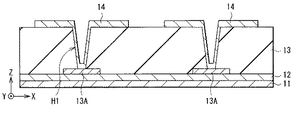
図1は、本技術の第1の実施の形態としての有機EL表示装置(表示装置1)の要部断面構成を表したものである。表示装置1は、基板11上に、トランジスタ(後述の図3のサンプリング用トランジスタ44Aおよび駆動用トランジスタ44B)を含むTFT層12、駆動配線13A、平坦化層13、中継電極14および有機発光素子20をこの順に有するものである。各有機発光素子20は、例えば赤(R),緑(G),青(B)の3つのサブピクセル(後述の図2の画素PXLC)のいずれかを構成しており、これらの3つのサブピクセルが1つのピクセルとして機能するようになっている。図1には、赤色光を発する赤色有機発光素子20Rおよび緑色光を発する緑色有機発光素子20Gを示したが、青色光を発する青色有機発光素子も、これらとほぼ同じ構造を有している。隣り合う有機発光素子20の間には、隔壁24が設けられている。このような有機発光素子20および隔壁24は封止層25で覆われている。有機発光素子20および封止層25を間にして基板11には、封止基板31が対向している。表示装置1は、有機発光素子20が発した光を封止基板31から取り出す、いわゆるトップエミッション型の表示装置である。
<First Embodiment>
[Overall Configuration of Display Device 1]
FIG. 1 illustrates a cross-sectional configuration of a main part of an organic EL display device (display device 1) as a first embodiment of the present technology. The
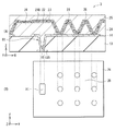
図2は、表示装置1の全体構成を表すものである。このように、例えば基板11上には、有機発光素子20(図1)を含む複数の画素PXLC(サブピクセル)がマトリクス状に配置されてなる表示領域40が形成され、この表示領域40の周辺に、信号線駆動回路としての水平セレクタ(HSEL)41と、走査線駆動回路としてのライトスキャナ(WSCN)42と、電源線駆動回路としての電源スキャナ(DSCN)43とが設けられている。
FIG. 2 shows the overall configuration of the
表示領域40において、列方向には複数(整数n個)の信号線DTL1〜DTLnが配置され、行方向には、複数(整数m個)の走査線WSL1〜WSLmおよび電源線DSL1〜DSLmがそれぞれ配置されている。また、各信号線DTLと各走査線WSLとの交差点に、各画素PXLC(R、G、Bに対応する画素のいずれか1つ)が設けられている。各信号線DTLは水平セレクタ41に接続され、この水平セレクタ41から各信号線DTLへ映像信号が供給されるようになっている。各走査線WSLはライトスキャナ42に接続され、このライトスキャナ42から各走査線WSLへ走査信号(選択パルス)が供給されるようになっている。各電源線DSLは電源スキャナ43に接続され、この電源スキャナ43から各電源線DSLへ電源信号(制御パルス)が供給されるようになっている。
In the
図3は、画素PXLCにおける具体的な回路構成例を表したものである。各画素PXLCは、有機発光素子20を含む画素回路50を有している。この画素回路50は、サンプリング用トランジスタ44Aおよび駆動用トランジスタ44Bと、保持容量素子44Cおよび補助容量素子44Dと、有機発光素子20とを有するアクティブ型の駆動回路である。
FIG. 3 illustrates a specific circuit configuration example in the pixel PXLC. Each pixel PXLC has a
サンプリング用トランジスタ44Aは、そのゲートが対応する走査線WSLに接続され、そのソースおよびドレインのうちの一方が対応する信号線DTLに接続され、他方が駆動用トランジスタ44Bのゲートに接続されている。駆動用トランジスタ44Bは、そのドレインが対応する電源線DSLに接続され、ソースが有機発光素子20のアノードに接続されている。また、この有機発光素子20のカソードは、接地配線44Hに接続されている。なお、この接地配線44Hは、全ての画素PXLCに対して共通に配線されている。保持容量素子44Cは、駆動用トランジスタ44Bのソースとゲートとの間に配置されている。補助容量素子44Dは、有機発光素子20のアノード(駆動用トランジスタ44Bのソース)と接地配線44Hとの間に配置されている。
サンプリング用トランジスタ44Aは、走査線WSLから供給される走査信号(選択パルス)に応じて導通することにより、信号線DTLから供給される映像信号の信号電位をサンプリングし、保持容量素子44Cに保持するものである。駆動用トランジスタ44Bは、所定の第1電位(図示せず)に設定された電源線DSLから電流の供給を受け、保持容量素子44Cに保持された信号電位に応じて、駆動電流を有機発光素子20へ供給するものである。有機発光素子20は、この駆動用トランジスタ44Bから供給された駆動電流により、映像信号の信号電位に応じた輝度で発光するようになっている。保持容量素子44Cは、有機発光素子20の容量不足分を補い、保持容量素子44Cに対する映像信号の書き込みゲインを高める役割を担っている。
The
[表示装置1の要部構成]
次に、再び図1を参照して、基板11、有機発光素子20および封止基板31等の詳細な構成について説明する。
[Configuration of main part of display device 1]
Next, with reference to FIG. 1 again, detailed configurations of the
基板11は、例えば、水分(水蒸気)および酸素の透過を遮断可能なガラスまたはプラスチック材料などにより形成されている。基板11は、その一主面に有機発光素子20が配列形成される支持体である。基板11の構成材料としては、例えば高歪点ガラス、ソーダガラス(Na2O・CaO・SiO2)、硼珪酸ガラス(Na2O・B2O3・SiO2)、フォルステライト(2MgO・SiO2)および鉛ガラス(Na2O・PbO・SiO2)等のガラス基板、石英基板あるいはシリコン基板が挙げられる。このようなガラス基板、石英基板およびシリコン基板の表面に絶縁膜を設けて基板11を構成してもよい。基板11には、金属箔もしくは樹脂製のフィルムやシートなどを用いることも可能である。樹脂の材質としては、例えば、ポリメチルメタクリレート(ポリメタクリル酸メチル,PMMA)、ポリビニルアルコール(PVA)、ポリビニルフェノール(PVP)、ポリエーテルスルホン(PES)、ポリイミド、ポリカーボネート、ポリエチレンテレフタレート(PET)およびポリエチレンナフタレート(PEN)などの有機ポリマーが挙げられる。なお、トップエミッション型では封止基板20から光が取り出されるため、基板11は、透過性材料または非透過性材料のいずれにより形成されていてもよい。封止基板20には基板11と同じ材料を用いるようにしてもよく、あるいは、異なる材料を用いるようにしてもよい。また、可撓性材料により基板11を構成してもよい。
The
TFT層12は、上記サンプリング用トランジスタ44Aおよび駆動用トランジスタ44Bを含み、有機発光素子20の能動素子として機能するものである。TFT層12のトランジスタの構成は、逆スタガ構造(ボトムゲート型)であっても、スタガ構造(トップゲート型)であってもよい。駆動用トランジスタ44Bのソースは、駆動配線13Aに電気的に接続されている。
The
平坦化層13は、TFT層12および駆動配線13Aが形成された基板11の表面を平坦化するためのものであり、例えばポリイミド,アクリル系樹脂またはノボラック系樹脂などの有機絶縁膜により構成されている。あるいは、無機絶縁膜、例えば酸化シリコン(SiOx),窒化シリコン(SiNx)および酸窒化シリコン(SiON)等のうちの少なくとも1種を含む単層膜あるいは積層膜より平坦化層13を構成するようにしてもよい。
The
平坦化層13には、接続孔H1が設けられている。この接続孔H1を介して、平坦化層13上の中継電極14と駆動配線13Aとが電気的に接続されている。この中継電極14は、駆動配線13Aと有機発光素子20との間に設けられ、駆動配線13Aと有機発光素子20(具体的には、後述の第1電極21)とを電気的に接続するためのものである。中継電極14は、平坦化層13上から接続孔H1の壁面(側面および底面)に沿うように設けられており、接続孔H1の底面で駆動配線13Aに接している。中継電極14は、有機発光素子20で発生する光に対して反射率の高い導電材料により構成されている。この中継電極14には、例えば厚み200nmのアルミニウム(Al)―ネオジム(Nd)合金を用いることができる。光反射性の中継電極14を用いることにより、正面への光取り出し効率を向上させることができる。
The
本実施の形態では、この接続孔H1内の中継電極14を覆うように、接続孔H1に穴埋め部材15が設けられている。詳細は後述するが、これにより、接続孔H1に起因する段差の大きさが小さくなり、接続孔H1に平面視で重なる位置に発光領域(後述の図4(B)の発光領域E)を配置することができる。
In the present embodiment, a filling
穴埋め部材15は、接続孔H1を塞ぐためのものであり、接続孔H1および接続孔H1の近傍に設けられている。穴埋め部材15の表面の位置(Z方向の位置)は、平坦化層13上の中継電極14の表面の位置に近いことが好ましい。穴埋め部材15の表面は、例えば、平坦化層13上の中継電極14の表面から隆起するように設けられ、平坦化層13上の中継電極14の表面よりも1μm以下程度、封止基板31に近い位置に設けられている。穴埋め部材15の表面は、平坦化層13上の中継電極14の表面よりもへこんでいてもよく、平坦化層13上の中継電極14の表面よりも基板11に近い位置に設けられていてもよい。穴埋め部材15は、例えば、ポリイミド,アクリル系樹脂およびノボラック系樹脂等の有機絶縁膜により構成されている。
The
平面視で、この穴埋め部材15上を含む領域に、有機発光素子20が設けられている。有機発光素子20は、平坦化層13(基板11)に近い位置から、第1電極21、発光層を含む有機層22および第2電極23をこの順に有している。
The organic
第1電極21は、穴埋め部材15を覆うように設けられ、接続孔H1の周囲で中継電極14に接している。図4は、接続孔H1近傍の詳細な構造を表したものであり、図4(A)は断面構成、図4(B)は平面構成をそれぞれ表している。接続孔H1では、穴埋め部材15を間にして中継電極14と第1電極21とが対向しており(図4(A))、平面視で接続孔H1と重なる位置に中継電極14、穴埋め部材15および第1電極21が設けられている(図4(B))。第1電極21および中継電極14は、有機発光素子20毎に分離して設けられている。中継電極14は、平面視で第1電極21よりも広い面積にわたって設けられ、第1電極21の周囲に拡幅している(図4(B))。
The
第1電極21は例えばアノード電極としての機能および反射層としての機能を兼ね備えたものであり、反射率が高く、かつ、正孔注入性も高い材料により構成されていることが望ましい。このような第1電極21としては、例えば、積層方向の厚み(以下、単に厚みと言う)が100nm〜300nmの導電材料を用いることができる。第1電極21の厚みは、例えば、中継電極14の厚みよりも小さい。第1電極21の構成材料としては、例えば、クロム(Cr),金(Au),白金(Pt),ニッケル(Ni),銅(Cu),モリブデン(Mo),タングステン(W),チタン(Ti),タンタル(Ta),アルミニウム(Al),鉄(Fe)あるいは銀(Ag)などの金属元素の単体または合金が挙げられる。第1電極21は、このような金属膜を複数積層したものであってもよい。銀に0.3重量%〜1重量%のパラジウム(Pd)と0.3重量%〜1重量%の銅とを含有させたAg―Pd―Cu合金あるいはAl―ネオジム(Nd)合金を第1電極21に用いるようにしてもよい。第1電極21には仕事関数の高い材料を用いることが好ましいが、アルミニウムおよびアルミニウム合金等の仕事関数の小さい金属であっても、適切な有機層22(特に、後述の正孔注入層)を選択することにより、第1電極21として用いることが可能となる。光透過性の高い導電材料により第1電極21を構成し、基板11と第1電極21との間に反射層を設けるようにしてもよい。
The
隣り合う第1電極21の間には、隔壁24が設けられている。この隔壁24は、平坦化層13上の中継電極14の端部を覆っており、中継電極14の周縁では中継電極14と有機層22との間に配置されている。このような隔壁24を設けることにより、隣り合う有機発光素子20が電気的に分離され、かつ、中継電極14と第2電極23との間の絶縁性も確保される。隔壁24が設けられていない領域では、第1電極21の表面と有機層22とが、あるいは中継電極14の表面と有機層22とが接している。この第1電極21と有機層22との接触領域、および中継電極14と有機層22との接触領域が発光領域(図4(B)の発光領域E)となる。このように、表示装置1では、隔壁24により有機発光素子20の発光領域Eの形状が制御されている。また、中継電極14の端部を覆う隔壁24は、中継電極14の厚みに起因した中継電極14と第2電極23との短絡を防ぐ役割を担っている。隔壁24は、有機発光素子20の光取り出し効率を高めるため、テーパ形状を有していることが好ましい。隔壁24は穴埋め部材15と同一材料により構成されており、例えば穴埋め部材15と同一工程で形成することができる。隔壁24の高さ(Z方向の距離)は、穴埋め部材15の高さと略同じであり、例えば1μm〜5μmである。
A
有機層22は、例えば、全ての有機発光素子20に共通して設けられ、第1電極21に近い位置から、正孔注入層,正孔輸送層,発光層,電子輸送層および電子注入層(いずれも図示せず)をこの順に有している。正孔輸送層,発光層および電子輸送層により有機層22を構成するようにしてもよく、このとき、発光層が電子輸送層を兼ねるようにしてもよい。このような一連の積層構造(いわゆるタンデムユニット)が接続層を介して複数重なることで有機層22が構成されてもよい。例えば、赤色、緑色、青色および白色の色毎にタンデムユニットを有し、これらを積層して有機層22を構成するようにしてもよい。有機層22の厚みは例えば100nm〜300nmである。
For example, the
正孔注入層は、正孔注入効率を高めるためのものであると共に、リークを防止するためのバッファ層である。正孔注入層は、例えば、厚みが1nm以上300nm以下であり、化1または化2に示したヘキサアザトリフェニレン誘導体により構成されている。
The hole injection layer is a buffer layer for improving hole injection efficiency and preventing leakage. The hole injection layer has, for example, a thickness of 1 nm to 300 nm and is made of the hexaazatriphenylene derivative shown in

正孔輸送層は、発光層への正孔輸送効率を高めるためのものである。正孔輸送層は、例えば、厚みが40nm程度であり、4,4′,4″−トリス(3−メチルフェニルフェニルアミノ)トリフェニルアミン(m−MTDATA)またはα−ナフチルフェニルジアミン(αNPD)により構成されている。 The hole transport layer is for increasing the efficiency of transporting holes to the light emitting layer. The hole transport layer has a thickness of about 40 nm, for example, and is made of 4,4 ′, 4 ″ -tris (3-methylphenylphenylamino) triphenylamine (m-MTDATA) or α-naphthylphenyldiamine (αNPD). It is configured.
発光層は例えば白色発光用の発光層であり、第1電極21と第2電極23との間、および中継連極14と第2電極23との間に例えば赤色発光層、緑色発光層および青色発光層(いずれも図示せず)の積層体を有している。赤色発光層,緑色発光層および青色発光層は、電界をかけることにより、第1電極21から正孔注入層および正孔輸送層を介して注入された正孔の一部と、第2電極23から電子注入層および電子輸送層を介して注入された電子の一部とが再結合して、それぞれ赤色,緑色および青色の光を発生させるものである。
The light emitting layer is a light emitting layer for white light emission, for example, between the
赤色発光層は、例えば、赤色発光材料,正孔輸送性材料,電子輸送性材料および両電荷輸送性材料のうち少なくとも1種を含んでいる。赤色発光材料は、蛍光性のものでも燐光性のものでもよい。赤色発光層は、例えば、厚みが5nm程度であり、4,4−ビス(2,2−ジフェニルビニン)ビフェニル(DPVBi)に2,6−ビス[(4’−メトキシジフェニルアミノ)スチリル]−1,5−ジシアノナフタレン(BSN)を30重量%混合したものにより構成されている。 The red light emitting layer includes, for example, at least one of a red light emitting material, a hole transporting material, an electron transporting material, and a both charge transporting material. The red light emitting material may be fluorescent or phosphorescent. The red light-emitting layer has, for example, a thickness of about 5 nm, and 2,4-bis [(4′-methoxydiphenylamino) styryl]-is added to 4,4-bis (2,2-diphenylbinine) biphenyl (DPVBi). It is composed of 30% by weight of 1,5-dicyanonaphthalene (BSN).
緑色発光層は、例えば、緑色発光材料,正孔輸送性材料,電子輸送性材料および両電荷輸送性材料のうち少なくとも1種を含んでいる。緑色発光材料は、蛍光性のものでも燐光性のものでもよい。緑色発光層は、例えば、厚みが10nm程度であり、DPVBiにクマリン6を5重量%混合したものにより構成されている。 The green light emitting layer includes, for example, at least one of a green light emitting material, a hole transporting material, an electron transporting material, and a charge transporting material. The green light emitting material may be fluorescent or phosphorescent. The green light emitting layer has a thickness of about 10 nm, for example, and is composed of DPVBi mixed with 5% by weight of coumarin 6.
青色発光層は、例えば、青色発光材料,正孔輸送性材料,電子輸送性材料および両電荷輸送性材料のうち少なくとも1種を含んでいる。青色発光材料は、蛍光性のものでも燐光性のものでもよい。青色発光層は、例えば、厚みが30nm程度であり、DPVBiに4,4’−ビス[2−{4−(N,N−ジフェニルアミノ)フェニル}ビニル]ビフェニル(DPAVBi)を2.5重量%混合したものにより構成されている。 The blue light emitting layer includes, for example, at least one of a blue light emitting material, a hole transporting material, an electron transporting material, and a charge transporting material. The blue light emitting material may be fluorescent or phosphorescent. For example, the blue light-emitting layer has a thickness of about 30 nm, and 2.5% by weight of 4,4′-bis [2- {4- (N, N-diphenylamino) phenyl} vinyl] biphenyl (DPAVBi) is added to DPVBi. It is composed of a mixture.
電子輸送層は、発光層への電子輸送効率を高めるためのものであり、例えば厚みが20nm程度のトリス8−ヒドロキシキノリンアルミニウム(Alq3)により構成されている。電子注入層は、発光層への電子注入効率を高めるためのものであり、例えばLiFあるいはLi2O等により構成されている。
The electron transport layer is for increasing the efficiency of electron transport to the light emitting layer, and is made of, for example, tris 8-hydroxyquinoline aluminum (Alq3) having a thickness of about 20 nm. The electron injection layer is for increasing the efficiency of electron injection into the light emitting layer, and is made of, for example, LiF or Li 2 O.
第2電極23は、有機層22を間にして第1電極21および中継電極14と対をなし、全ての有機発光素子20に共通して設けられている。第2電極23は例えばカソード電極としての機能および光透過層としての機能を兼ね備えたものであり、導電性が高く、かつ、光透過率も高い材料により構成されていることが望ましい。したがって、第2電極23は、例えば、アルミニウム(Al),マグネシウム(Mg),銀(Ag),カルシウム(Ca)またはナトリウム(Na)の合金により構成されている。中でも、マグネシウムと銀との合金(Mg−Ag合金)は、薄膜での導電性と吸収の小ささとを兼ね備えているので好ましい。Mg−Ag合金におけるマグネシウムと銀との比率は特に限定されないが、膜厚比でMg:Ag=20:1〜1:1の範囲であることが望ましい。また、第2電極23の材料には、アルミニウム(Al)とリチウム(Li)との合金(Al−Li合金)を用いるようにしてもよく、インジウム錫酸化物(ITO),酸化亜鉛(ZnO),アルミナドープ酸化亜鉛(AZO),ガリウムドープ酸化亜鉛(GZO),インジウム亜鉛酸化物(IZO),インジウムチタン酸化物(ITiO)またはインジウムタングステン酸化物(IWO)等を用いてもよい。第2電極23は、複数の膜を積層させて構成するようにしてもよい。例えば、カルシウム,バリウム(Ba),リチウム,セシウム(Cs),インジウム(In),マグネシウムまたは銀等からなる膜に、マグネシウム,銀,あるいは、マグネシウムまたは銀を含む合金からなる膜を積層させて第2電極23を構成するようにしてもよい。第2電極23の厚みは、例えば50nm〜500nm程度である。
The
有機層22と第2電極23との間に高抵抗層(図示せず)を設けるようにしてもよい。高抵抗層は、第1電極21および中継電極14と第2電極23との間の短絡の発生を防止するためのものであり、全ての有機発光素子20に共通して設けられている。高抵抗層は、第1電極21および第2電極23よりも電気抵抗が高く、電荷の輸送機能あるいは電荷の注入機能を備えている。第1電極21上に意図せずパーティクル(異物)や突起物が付着し、その状態で有機発光素子1を形成した場合、第1電極21と第2電極23との接触による短絡が生じるおそれがある。高抵抗層により、このような第1電極21と第2電極23との接触を防ぐことができる。
A high resistance layer (not shown) may be provided between the
高抵抗層は、例えば、電気抵抗率が1×10⁶Ω・m以上1×10⁸Ω・m以下の材料により構成されていることが好ましい。この範囲内であれば、十分に短絡の発生を防止し、かつ、駆動電圧を低く抑えることができるためである。高抵抗層は、例えば、酸化ニオブ(Nb2O5),酸化チタン(TiO2),酸化モリブデン(MoO2,MoO3),酸化タンタル(Ta2O5),酸化ハフニウム(HfO),酸化マグネシウム(MgO),IGZO(InGaZnOx),酸化ニオブと酸化チタンとの混合物,酸化チタンと酸化亜鉛(ZnO)との混合物,酸化ケイ素(SiO2)と酸化錫(SnO2)との混合物または酸化亜鉛に酸化マグネシウム、酸化ケイ素あるいは酸化アルミニウム(Al2O3)のうちから少なくとも1つを混合した混合物により構成されている。これらの材料を適宜組み合わせて高抵抗層を構成するようにしてもよい。有機層22および第2電極23の屈折率に近い値、例えば屈折率1.7以上の高抵抗層を用いることが好ましく、1.9以上であることがより好ましい。これにより、有機層22の発光層の外部量子効率が向上する。高抵抗層の厚みは、例えば100nm〜1000nm程度である。
The high resistance layer is preferably made of, for example, a material having an electrical resistivity of 1 × 10 6 Ω · m to 1 × 10 8 Ω · m. This is because if it is within this range, the occurrence of a short circuit can be sufficiently prevented and the drive voltage can be kept low. The high resistance layer is, for example, niobium oxide (Nb 2 O 5 ), titanium oxide (TiO 2 ), molybdenum oxide (MoO 2 , MoO 3 ), tantalum oxide (Ta 2 O 5 ), hafnium oxide (HfO), magnesium oxide. (MgO), IGZO (InGaZnO x ), a mixture of niobium oxide and titanium oxide, a mixture of titanium oxide and zinc oxide (ZnO), a mixture of silicon oxide (SiO 2 ) and tin oxide (SnO 2 ), or zinc oxide And at least one of magnesium oxide, silicon oxide and aluminum oxide (Al 2 O 3 ). You may make it comprise a high resistance layer combining these materials suitably. It is preferable to use a high resistance layer having a value close to the refractive index of the
第2電極23上には、保護層(図示せず)が設けられている。この保護層は、有機層22への水分の侵入を防ぐと共に、表示装置1の機械的強度を高めるためのものである。保護層は、光透過性が高く、かつ、透水性の低い材料により構成されており、例えばその厚みは5μm〜15μmである。保護層には、絶縁性材料および導電性材料のいずれを用いるようにしてもよい。保護層には、例えば、窒化ケイ素(SiNX),酸化ケイ素(SiOX),酸化アルミニウム(AlOX)またはこれらの組み合わせを用いることができる。保護層上には封止層25を間にして封止基板31が貼り合わされている。封止層25は、例えば熱硬化型樹脂または紫外線硬化型樹脂などにより構成されている。
A protective layer (not shown) is provided on the
封止基板31は、保護層と共に、各有機発光素子20を封止するためのものであり、例えば、赤色,緑色,青色の各色光に対して透明な材料、例えばガラスなどにより構成されている。封止基板31の基板11との対向面には、カラーフィルタ32および遮光層33が設けられており、これらがオーバーコート層34により覆われている。
The sealing
カラーフィルタ32は、例えば、赤色フィルタ32R、緑色フィルタ32Gおよび青色フィルタ(図示せず)を含み、これらが遮光層33および有機発光素子20のパターン毎に配色されている。遮光層33に重なる位置にカラーフィルタ32が設けられていてもよい。赤色フィルタ32R、緑色フィルタ32Gおよび青色フィルタは、例えば顔料または染料を混入した樹脂により構成されている。この顔料または染料の種類を適宜選択することにより、赤色フィルタ32R、緑色フィルタ32Gおよび青色フィルタではそれぞれ、赤色、緑色または青色それぞれの波長域の光透過率が高くなるように調整されている。赤色、緑色および青色の目的とする波長域以外では、カラーフィルタ32の光透過率は低くなっている。カラーフィルタ32の厚みは例えば、1〜4μmである。カラーフィルタ32を、封止基板31の面のうち、基板11との対向面と反対の面に設けるようにしてもよいが、基板11との対向面に設けることが好ましい。カラーフィルタ32が表面に露出せず、封止層25等により保護することができるからである。また、有機層22とカラーフィルタ32との間の距離が狭くなることにより、有機層22から出射した光が隣接する他の色のカラーフィルタに入射して混色を生じることを避けることができるからである。
The
遮光層33は、いわゆるブラックマトリクス(BM)である。この遮光層33は、表示領域40(図2)では画素PXLCの配置に合わせて、例えばマトリクス状にパターニングされている。遮光層33は、例えばカーボンブラックにより構成される。遮光性と導電性を兼ねた材料、クロムおよびグラファイト等を遮光層33に用いるようにしてもよい。あるいは、薄膜の干渉を利用した薄膜フィルタにより遮光層33を構成するようにしてもよい。この薄膜フィルタは、例えば、金属、金属窒化物または金属酸化物等の薄膜を1層以上積層することにより、薄膜の干渉を生じさせて光を減衰させるものである。このような薄膜フィルタとしては、例えば、封止基板31に近い位置から、窒化シリコン(SiN)65nm、アモルファスシリコン(a−Si)20nmおよびモリブデン(Mo)50nm以上をこの順に積層させたもの、あるいは、封止基板31に近い位置から、酸化モリブデン(MoOx)45nm、モリブデン10nm、酸化モリブデン40nmおよびモリブデン(Mo)50nm以上をこの順に積層させたもの等を挙げることができる。
The
オーバーコート層34は、カラーフィルタ32表面の平坦性を高め、保護するためのコーティング剤であり、例えば樹脂等の有機材料やSiO,SiNあるいはITOなどの無機材料により構成されている。
The
[製造方法]
上記のような表示装置1は、例えば次のようにして製造することができる(図5A〜図6B)。
[Production method]
The
(TFT層および平坦化層の形成工程)
まず、基板11上に、所定の薄膜プロセスを経てTFT層12を含む駆動回路および駆動配線13Aを形成した後、基板11の全面にわたって平坦化層13を、例えばスピンコート法またはスリットコート法により成膜する。続いて、成膜した平坦化層13を、例えばフォトリソグラフィ法により、所定の形状にパターニングして平坦化層13に接続孔H1を形成する(図5A)。
(TFT layer and planarization layer forming process)
First, after a driving circuit and a driving
(中継電極の形成工程)
次いで、平坦化層13上にスパッタ法を用いて例えばAl−Nd合金を基板11の全面に成膜した後、これをフォトリソグラフィ法を用いてパターニングし、中継電極14を形成する(図5B)。このとき、中継電極14を平坦化層13の接続孔H1を介して、駆動配線13Aに電気的に接続させる。
(Relay electrode formation process)
Next, an Al—Nd alloy, for example, is formed on the entire surface of the
(穴埋め部材および隔壁の形成工程)
中継電極14を設けた後、図5Cに示したように、接続孔H1に穴埋め部材15を形成するとともに、平坦化層13上には隔壁24を形成する。具体的には、まず、例えば感光性樹脂材料を、スピンコート法により接続孔H1内と、平坦化層13上および中継電極14上に成膜する。次いで、所定のフォトマスクを用いて露光した後、現像し、感光性樹脂膜をウェットエッチング法を用いてパターニングする。これにより、同一工程で穴埋め部材15および隔壁24が形成される。穴埋め部材15を形成することにより、平坦化層13の接続孔H1が埋められ、接続孔H1に起因する段差の大きさが小さくなる。穴埋め部材15および隔壁24の形成にウェットエッチング法を用いることにより、穴埋め部材15および隔壁24の形状はテーパ状となる。
(Process for forming hole filling member and partition wall)
After providing the
(有機発光素子の形成工程)
続いて、図6Aに示したように、穴埋め部材15上から中継電極14上にわたって第1電極21を形成する。第1電極21は、例えばAlNd合金をスパッタ法により基板11全面にわたって成膜した後、例えばフォトリソグラフィ法を用いてパターニングすることにより形成される。このとき、中継電極14に接触するように第1電極21を形成することにより、第1電極21を中継電極14に電気的に接続させる。その後、例えば真空蒸着法等の物理的気相成長法(PVD法:Physical Vapor Deposition)により発光層を含む有機層22および第2電極23を基板11上の表示領域40の全面に形成する(図6B)。有機層22および第2電極23は、スクリーン印刷法およびインクジェット印刷法等の印刷法、レーザ転写法あるいは塗布法等により形成するようにしてもよい。
(Formation process of organic light emitting device)
Subsequently, as illustrated in FIG. 6A, the
(封止基板の形成工程)
封止基板31上には、例えば以下のようにして遮光層33、カラーフィルタ32、およびオーバーコート層34を形成する。まず、封止基板31の全面に遮光層33の構成材料を成膜したのち、これを例えばフォトリソグラフィ工程を用いてマトリクス状にパターニングし、画素PXLCの配置に合わせた開口を複数形成する。これにより遮光層33が形成される。次いで、遮光層33の開口に赤色フィルタ32R、緑色フィルタ32Gおよび青色フィルタを順次パターニングして設け、カラーフィルタ32を形成する。その後、このカラーフィルタ32を設けた封止基板31の全面にオーバーコート層34を成膜する。
(Sealing substrate formation process)
On the sealing
(基板と封止基板との貼り合わせ工程)
上記のようにして形成した封止基板31は、例えばODF(One Drop Fill)工程により有機発光素子20および封止層25を間にして、基板11に貼り合わされる。以上により、図1に示した表示装置1が完成する。
(Bonding process of substrate and sealing substrate)
The sealing
[表示装置1の動作]
表示装置1では、各有機発光素子20に、各色の映像信号に応じた駆動電流が印加されると、第1電極21および第2電極23、または中継電極14および第2電極23を通じて、有機層22に電子および正孔が注入される。これらの電子および正孔は、有機層22に含まれる発光層においてそれぞれ再結合され、発光を生じる。この光は第1電極21および中継電極14で反射され、第2電極23,カラーフィルタ32および封止基板31を透過して外部へ取り出される。このようにして、表示装置1では、例えばR,G,Bのフルカラーの映像表示がなされる。また、この映像表示動作の際に保持容量素子44C(図3)の一端に、映像信号に対応する電位が印加されることにより、保持容量素子44Cには、映像信号に対応する電荷が蓄積される。
[Operation of display device 1]
In the
ここで、表示装置1では、平坦化層13の接続孔H1に穴埋め部材15が設けられているので、接続孔H1に起因する段差の大きさが小さくなり、この接続孔H1と平面視で重なる位置に発光領域E(図4(B))を形成することが可能となる。以下、これについて説明する。
Here, in the
(比較例)
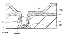
図7は比較例1に係る表示装置(表示装置100)の要部の構成を表している。図7(A)は表示装置100の断面構成、図7(B)は表示装置100の平面構成をそれぞれ表している。この表示装置100には、中継電極が設けられておらず、第1電極(第1電極121)が平坦化層13の接続孔H1を介して駆動配線13Aに接続されている。接続孔H1の直上には、隔壁(隔壁124)が設けられており、接続孔H1と平面視で重なる領域では、第1電極121と有機層22とが電気的に分離されている。即ち、平面視で接続孔H1と重なる領域は非発光領域であり、発光領域Eは接続孔H1の位置を避けるように配置される。
(Comparative example)
FIG. 7 illustrates a configuration of a main part of the display device (display device 100) according to Comparative Example 1. FIG. 7A illustrates a cross-sectional configuration of the
図8は、平面視で接続孔H1に重なる領域にも発光領域Eを形成した表示装置(比較例2の表示装置100A)の構成を表すものである。図8(A)は表示装置100Aの断面構成、図8(B)は表示装置100Aの平面構成をそれぞれ表している。このように、接続孔H1上に隔壁(隔壁124A)を形成せずに、第1電極121、有機層22および第2電極23を成膜すると、図9に示したように、接続孔H1の段差に起因して第1電極121と第2電極23とが短絡し(短絡部S)、正常に発光しない虞がある。詳細には、急激な傾斜を有する接続孔H1の壁面に、有機層22を一定の厚みで成膜することが困難であり、一部有機層22が分断される。この有機層22の分断部分で第1電極121と第2電極23とが短絡する。特に、有機層22を蒸着法により成膜する場合には、第1電極121と第2電極23とが接続孔H1で短絡しやすくなる。
FIG. 8 illustrates a configuration of a display device (
これに対し、表示装置1では、平坦化層13の接続孔H1に穴埋め部材15が設けられているので、接続孔H1の壁面が穴埋め部材15で覆われ、接続孔H1に起因する段差の大きさが小さくなる。したがって、接続孔H1と平面視で重なる位置に、所定の厚みで有機層22が形成されやすくなる。穴埋め部材15を覆う位置に設けた第1電極21が、中継電極14を介して駆動配線13Aに電気的に接続されており、この第1電極21上に有機層22および第2電極23が設けられているので、接続孔H1上で発光が生じる。即ち、平面視で接続孔H1と重なる領域が発光領域Eとなる。
On the other hand, in the
このように、接続孔H1の位置に関わらず発光領域Eを自由に配置することができるので、表示装置1では、画素領域の面積を小さくし、高精細化が可能になる。また、画素領域に対する発光領域Eの比を大きくすることも可能になる。以下、これについて説明する。
Thus, since the light emitting region E can be freely arranged regardless of the position of the connection hole H1, in the
図10および図11は、画素(例えば、図3の画素PXLC)における発光領域Eの平面形状を表したものである。図10(A)および図11(A)は、接続孔H1を避けて発光領域Eを形成した画素、図10(B)および図11(B)は接続孔H1を含む領域に発光領域Eを形成した画素をそれぞれ表している。画素の周縁から発光領域Eまでは、例えば距離Lmだけ離間している。 10 and 11 show a planar shape of the light emitting region E in a pixel (for example, the pixel PXLC in FIG. 3). FIGS. 10A and 11A show pixels in which the light emitting region E is formed avoiding the connection hole H1, and FIGS. 10B and 11B show the light emitting region E in the region including the connection hole H1. Each formed pixel is shown. The distance from the periphery of the pixel to the light emitting region E is, for example, a distance Lm.
図10(A)の発光領域Eの面積および図10(B)の発光領域Eの面積は同じである。このとき、図10(B)では、接続孔H1の周囲の非発光領域がなくなるので、画素領域(画素領域P2)自体の面積を図10(A)の画素領域(画素領域P1)の面積に比べて小さくすることができる。即ち、画素領域P2を有する表示装置では、高精細化が可能となる。 The area of the light emitting region E in FIG. 10A and the area of the light emitting region E in FIG. 10B are the same. At this time, in FIG. 10B, there is no non-light emitting region around the connection hole H1, so the area of the pixel region (pixel region P2) itself is set to the area of the pixel region (pixel region P1) of FIG. It can be made smaller. That is, in the display device having the pixel region P2, high definition can be achieved.
一方、図11(A)および図11(B)では、画素領域(画素領域P1)の面積は同じである。このとき、図11(B)では、発光領域Eが接続孔H1に重なる部分にも広がるので、画素領域P1に対する発光領域Eの比を図11(A)に比べて高くすることができる。このように画素領域P1に対する発光領域Eの比を高めることにより、有機発光素子20の電流密度を小さくすることができる。
On the other hand, in FIGS. 11A and 11B, the area of the pixel region (pixel region P1) is the same. At this time, in FIG. 11B, since the light emitting region E extends to a portion overlapping the connection hole H1, the ratio of the light emitting region E to the pixel region P1 can be made higher than that in FIG. Thus, the current density of the organic
図12は、電流密度の大きさと有機発光素子の輝度劣化との関係を表したものである。破線が、電流密度の比較的大きな有機発光素子の輝度劣化を表し、実線が電流密度の比較的小さな有機発光素子の輝度劣化を表している。このように、電流密度を小さくすることにより、有機発光素子の輝度劣化を抑えることが可能となる。 FIG. 12 shows the relationship between the magnitude of the current density and the luminance deterioration of the organic light emitting element. The broken line represents the luminance deterioration of the organic light emitting element having a relatively large current density, and the solid line represents the luminance deterioration of the organic light emitting element having a relatively small current density. Thus, by reducing the current density, it is possible to suppress the luminance deterioration of the organic light emitting element.
以上のように本実施の形態では、平坦化層13の接続孔H1に穴埋め部材15を設けるようにしたので、より自由に発光領域Eを配置することが可能となる。よって、表示装置1では高精細化が可能となる。また、画素領域に対する発光領域Eの比を高め、有機発光素子20の電流密度を小さくすることも可能である。
As described above, in the present embodiment, since the
更に、穴埋め部材15の構成材料は、隔壁24の構成材料と同じであり、これらは同一工程で形成できるので、工程数の増加を抑えることができる。
Furthermore, the constituent material of the
以下、上記第1の実施の形態の変形例および他の実施の形態について説明するが、上記第1の実施の形態における構成要素と同一のものには同一の符号を付し、適宜説明を省略する。 Hereinafter, modifications of the first embodiment and other embodiments will be described, but the same components as those in the first embodiment are denoted by the same reference numerals, and description thereof will be omitted as appropriate. To do.
<変形例1>
図13は、変形例1に係る表示装置(表示装置1A)の要部の断面構成を表したものである。この表示装置1Aでは、第1電極(第1電極21A)が光透過性材料により構成されている。この点を除き、表示装置1Aは表示装置1と同様の構成を有し、その作用および効果も同様である。
<
FIG. 13 illustrates a cross-sectional configuration of a main part of a display device (display device 1A) according to the first modification. In the display device 1A, the first electrode (first electrode 21A) is made of a light transmissive material. Except for this point, the display device 1A has the same configuration as the
この第1電極21Aには、例えば、上述の第2電極23の材料で例示した導電材料を用いることができる。中継電極14は、表示装置1で説明したのと同様に、高反射性材料により構成されている。具体的に、中継電極14には、上記表示装置1の第1電極21で例示した、光反射性の導電材料を用いることができる。
For the first electrode 21A, for example, a conductive material exemplified as the material of the
このような表示装置1Aでは、有機発光素子20で生じた光のうち、中継電極14に向かう光(光L1)が平坦化層13の接続孔H1内で、中継電極14により反射される。この中継電極14での反射により、光L1は集光され、光透過性の第1電極21Aを透過して封止基板31(図1)から取り出される。したがって、表示装置1Aでは、正面輝度を向上させることが可能となる。
In such a
<変形例2>
図14は、変形例2に係る表示装置(表示装置1B)の要部の断面構成を表したものである。このように、一つの中継電極14を複数の接続孔H1で駆動配線13Aに接続するようにしてもよい。このとき、各々の接続孔H1に穴埋め部材15が設けられる。光透過性の第1電極(図13の第1電極21A)と光反射性の中継電極14とを組み合わせて用いる場合には、複数の接続孔H1を設けることにより、より正面輝度を向上させることが可能となる。
<
FIG. 14 illustrates a cross-sectional configuration of a main part of a display device (display device 1B) according to
<変形例3>
図15は、変形例3に係る表示装置(表示装置1C)の要部の断面構成を表したものである。この表示装置1Cの中継電極14は、保持容量素子(図3の保持容量素子44C)の一方の電極としても機能する。この点を除き、表示装置1Cは表示装置1と同様の構成を有し、その作用および効果も同様である。
<
FIG. 15 illustrates a cross-sectional configuration of a main part of a display device (display device 1C) according to
表示装置1Cは、例えば、駆動配線13Aと同層に、容量電極13Bを有している。この容量電極13Bは、中継電極14の一部の領域と対向する位置に設けられている。平坦化層13には、この容量電極13Bに対向する位置に平坦化層13を貫通する孔H2が設けられている。この平坦化層13の孔H2と容量電極13Bとの間には容量絶縁膜13Iが設けられている。即ち、孔H2では、容量絶縁膜13Iを間にして中継電極14と容量電極13Bとが対向しており、保持容量素子が構成されている。接続孔H1は、容量絶縁膜13Iを貫通して、中継電極14と駆動配線13Aとを電気的に接続する。
The display device 1C includes, for example, a capacitor electrode 13B in the same layer as the
<変形例4>
図16は、変形例4に係る表示装置(表示装置1D)の要部の断面構成を表したものである。この表示装置1Dでは、中継電極14の端部と共に第1電極21の端部が隔壁24で覆われている。この点を除き、表示装置1Dは表示装置1と同様の構成を有し、その作用および効果も同様である。
<Modification 4>
FIG. 16 illustrates a cross-sectional configuration of a main part of a display device (display device 1D) according to Modification 4. In the
第1電極21は、例えば、平面視で中継電極14よりも広い領域にわたって延在し、中継電極14の端面を覆っている。即ち、第1電極21の端部は、中継電極14の端部よりも外側に設けられている。表示装置1Dでは、隔壁24により、この第1電極21の端部が覆われているので、第1電極21の厚みに起因した第1電極21と第2電極23との短絡の発生が抑えられる。以下、これについて説明する。
For example, the
第1電極21の端部が隔壁24で覆われていない場合(例えば図1)には、第1電極21の端部が露出され、この第1電極21の端部上にも有機層22および第2電極23が積層される。第1電極21の端部では、第1電極21の厚み分の段差があるので、有機層22が分断され、第1電極21と第2電極23との短絡が生じる虞がある。この第1電極21の端部を隔壁24で覆うことにより、第1電極21の厚みに起因する第1電極21と第2電極23との短絡の発生を防ぐことが可能となる。
When the end portion of the
このような隔壁24は、例えば、穴埋め部材15および第1電極21を設けた後に、形成する。第1電極21の端部は、隔壁24で覆われていればよく、中継電極14の端部よりも内側に設けられていてもよい。
Such a
<変形例5>
図17は、変形例5に係る表示装置(表示装置1E)の断面構成を表したものである。この表示装置1Eは、隔壁24の側面に反射部材26(第1反射部材)を有するものである。この点を除き、表示装置1Eは表示装置1と同様の構成を有し、その作用および効果も同様である。
<Modification 5>
FIG. 17 illustrates a cross-sectional configuration of a display device (
反射部材26は、有機発光素子20で発生した光を反射するためのものであり、例えば隔壁24の上面から側面にわたり、設けられている。反射部材26は、例えば、上述の第1電極21の材料と同様の材料により構成されており、その厚みは10nm〜100nm程度である。このような反射部材26は、第1電極21と同一工程で形成することが可能である。
The
図18に示したように、有機発光素子20で発生した光のうち、隔壁24に向かう光(光L2)は、反射部材26で反射された後、封止基板31から取り出される。このように、反射部材26で光L2が反射されるので、混色の発生が抑えられる。
As shown in FIG. 18, among the light generated in the organic
図19に示したように、反射部材がない場合には、有機発光素子20で発生した光のうち、隔壁24に向かう光(光L3)は、隔壁24を透過するので、例えば赤の画素PXLCを構成する有機発光素子20Rで発生した光が、緑色フィルタ32Gを透過して取り出される虞がある。このような光L3は、隣接する緑の画素PXLCへの漏れ光となり、混色の原因となる。
As shown in FIG. 19, when there is no reflecting member, the light (light L3) that travels toward the
これに対し、隔壁24の側面を反射部材26で覆うことにより、光L2は反射部材26で反射されて、各画素PXLCの中心部に向かうようになる。したがって、隣接する画素PXLCへの漏れ光を防ぎ、混色の発生を抑えることができる。また、表示装置1Eでは正面輝度を向上させることも可能である。
On the other hand, by covering the side surface of the
反射部材26は、隔壁24の各側面に分離して設けられていてもよく(図17)、図20に示したように、隔壁24の上面から各側面にかけて一体化して設けられていてもよい。
The
<第2の実施の形態>
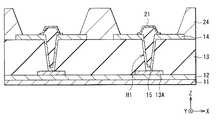
図21は本技術の第2の実施の形態に係る表示装置(表示装置2)の要部の断面構成を表したものであり、図21(A)は断面構成、図21(B)は平面構成をそれぞれ表している。この表示装置2では、第1電極(第1電極21B)が隔壁24上に延在しており、第1電極21Bにより発光領域Eの形状が制御されている。この点を除き、表示装置2は表示装置1と同様の構成を有し、その作用および効果も同様である。
<Second Embodiment>
FIG. 21 illustrates a cross-sectional configuration of a main part of a display device (display device 2) according to a second embodiment of the present technology, FIG. 21 (A) is a cross-sectional configuration, and FIG. 21 (B) is a plan view. Each configuration is shown. In the
第1電極21Bは、例えば、平面視で中継電極14よりも広い領域にわたって設けられている(図21(B))。この第1電極21Bは、穴埋め部材15を覆うとともに、穴埋め部材15の周囲に延在して隔壁24の側面も覆っている。この第1電極21Bにより覆われた隔壁24上では発光が生じ、第1電極21Bが設けられた領域が発光領域Eとなる。
For example, the
図22に示したように、光反射性材料により第1電極21Bを構成すると、有機発光素子20で発生した光のうち、隔壁24に向かう光L2は、隔壁24の側面の第1電極21Bで反射された後、封止基板31から取り出される。したがって、上記表示装置1Eで説明したのと同様にして、混色の発生が抑えられ、また、正面輝度を向上させることも可能となる。
As shown in FIG. 22, when the
<変形例6>
図23は、変形例6に係る表示装置(表示装置2A)の断面構成を表したものである。この表示装置2Aでは、穴埋め部材15と隔壁24とが接しており、これらが一体化されている。この点を除き、表示装置2Aは表示装置2と同様の構成を有し、その作用および効果も同様である。
<Modification 6>
FIG. 23 illustrates a cross-sectional configuration of a display device (display device 2A) according to Modification 6. In the display device 2A, the
例えば、互いに高さの異なる穴埋め部材15と隔壁24とが、徐々に高さを変化させながら一体化されている(図23)。
For example, the
図24に示したように、穴埋め部材15の高さを隔壁24の高さと同じにして、これらを一体化させるようにしてもよい。
As shown in FIG. 24, the height of the
<変形例7>
図25は、変形例7に係る表示装置(表示装置2B)の断面構成を表したものである。この表示装置2Bでは、第1電極21Bの端部が隔壁27(第2隔壁)で覆われている。この点を除き、表示装置2Bは表示装置2と同様の構成を有し、その作用および効果も同様である。
<Modification 7>
FIG. 25 illustrates a cross-sectional configuration of a display device (display device 2B) according to Modification 7. In the display device 2B, the end portion of the
隔壁27には、例えば上述の隔壁24と同様の絶縁材料を用いることができる。このような隔壁27が隔壁24上に設けられ、第1電極21Bの端部を覆っている。隔壁27は、隔壁24上に第1電極21Bを設けた後、基板11の全面に絶縁材料を成膜し、これを例えばフォトリソグラフィ法を用いてパターニングすることにより形成することができる。
For the
このような隔壁27を設けることにより、上記表示装置1Dで説明したのと同様に、第1電極21Bの厚みに起因する第1電極21Bと第2電極23との短絡の発生を防ぐことが可能となる。
By providing such a
<第3の実施の形態>
図26は本技術の第3の実施の形態に係る表示装置(表示装置3)の要部の断面構成を表したものである。この表示装置3は、中継電極14の両端部に設けられた隔壁24間に、更に隔壁28(第3隔壁)を有するものである。この点を除き、表示装置3は表示装置1と同様の構成を有し、その作用および効果も同様である。
<Third Embodiment>
FIG. 26 illustrates a cross-sectional configuration of a main part of a display device (display device 3) according to the third embodiment of the present technology. The
隔壁28は中継電極14の表面の一部を覆うように設けられている。隔壁28は、一つの中継電極14に一つ設けるようにしてもよく(図示せず)、あるいは、一つの中継電極14に複数の隔壁28を設けるようにしてもよい。複数の隔壁28は、所定の間隙で中継電極14上に配置される。図26には、中継電極14の両端部に設けられた隔壁24間に、3つの隔壁28を設けた場合を図示したが、隔壁28の数はいくつであってもよい。このような隔壁28を設けることにより、中継電極14の表面に凹凸が形成される。隔壁28は、例えば、上述の隔壁24と同一材料により構成されており、隔壁24の高さと同一の高さを有している。隔壁28は、例えば、隔壁24と同一工程で形成することができる。
The
図27、図28および図29は、隔壁24,28の構成の一例を表したものである。図27(A)、図28(A)および図29(A)は隔壁24,28の断面構成例、図27(B)、図28(B)および図29(B)は隔壁24,28の平面構成例をそれぞれ表している。図27(B)に示したように、隔壁24と隔壁28とを一体化させるようにしてもよい。このとき、中継電極14と第1電極21Bとは、例えばドット状等の島状の領域で接触する。あるいは、図28(B)および図29(B)に示したように、隔壁24と隔壁28とが分離されていてもよい。隔壁28は、例えば、接続孔H1の周囲に四角形状に形成するようにしてもよく(図28(B))、円状に形成するようにしてもよい(図29(B))。
27, 28 and 29 show an example of the configuration of the
第1電極21Bは隔壁28を覆い(図26)、この第1電極21B上に有機層22および第2電極23が積層されている。このように、凹凸面に沿って形成した有機層22の表面積は、平坦面に設けた有機層22(例えば図21の表示装置2参照)の表面積に比べて大きくなる。これにより、補助容量素子44D(図3)の容量を増加させることが可能となる。
The
この表示装置3では、第1電極21Bの設けられた領域が発光領域Eであり、隔壁28上からも発光が生じる。
In the
図30に示したように、光反射性材料により第1電極21Bを構成すると、有機発光素子20で発生した光のうち、隔壁28に向かう光(光L4)は、隔壁28の側面の第1電極21Bで反射された後、封止基板31から取り出される。したがって、上記表示装置1Eで説明したのと同様にして、混色の発生が抑えられ、また、正面輝度を向上させることも可能となる。
As shown in FIG. 30, when the
図31,図32および図33に示したように、穴埋め部材15と隔壁24とが一体化されていてもよい。図31(A)、図32(A)および図33(A)は隔壁24,28の断面構成例、図31(B)、図32(B)および図33(B)は隔壁24,28の平面構成例をそれぞれ表している。上記図27、図28および図29で説明したのと同様にして、隔壁24と隔壁28とを一体化させるようにしてもよく(図31)、隔壁24と隔壁28とが分離されていてもよい(図32、図33)。
As shown in FIGS. 31, 32, and 33, the
また、図34に示したように、第1電極21Bの端部を覆う隔壁27を設けるようにしてもよい。
Further, as shown in FIG. 34, a
<変形例8>
図35は、変形例8に係る表示装置(表示装置3A)の断面構成を表したものである。この表示装置3Aは、隔壁28の側面に反射部材26(第2反射部材)を有するものである。この点を除き、表示装置3Aは表示装置3と同様の構成を有し、その作用および効果も同様である。
<Modification 8>
FIG. 35 illustrates a cross-sectional configuration of a display device (
表示装置3Aの第1電極21Bは、接続孔H1上およびその近傍に設けられ、隔壁24,28の側面には設けられていない。この隔壁24,28の側面が反射部材26で覆われている。
The
接続孔H1上およびその近傍では、第1電極21B、有機層22および第2電極23がこの順に積層され、隔壁24,28の間隙(隔壁28間および隔壁28と隔壁24との間)では、中継電極14、有機層22および第2電極23がこの順に積層されている。したがって、表示装置3Aでは、接続孔H1上およびその近傍と、隔壁24,28の間隙とで発光が生じるようになっている。
On the connection hole H1 and in the vicinity thereof, the
図36に示したように、表示装置3Aでは、有機発光素子20で発生した光のうち、隔壁28に向かう光L4は、隔壁28の側面の反射部材26で反射された後、封止基板31から取り出される。したがって、上記表示装置1Eで説明したのと同様にして、混色の発生が抑えられ、また、正面輝度を向上させることも可能となる。
As shown in FIG. 36, in the
<変形例9>
図37は、変形例9に係る表示装置(表示装置3B)の断面構成を表したものである。この表示装置3Bでは、中継電極14の端部と共に第1電極21の端部が隔壁24で覆われている。この点を除き、表示装置3Bは表示装置3と同様の構成を有し、その作用および効果も同様である。
<Modification 9>
FIG. 37 illustrates a cross-sectional configuration of a display device (display device 3B) according to Modification 9. In the
表示装置3Bの第1電極21は、隔壁28を覆っている。即ち、隔壁28の側面には第1電極21が設けられている。第1電極21は、例えば、平面視で中継電極14よりも広い領域にわたって延在し、中継電極14の端面を覆っている。このように隔壁24により第1電極21の端部が覆われた表示装置3Bでは、表示装置1D(図16)で説明したのと同様に、第1電極21の厚みに起因した第1電極21と第2電極23との短絡の発生が抑えられる。
The
<第4の実施の形態>
図38は本技術の第4の実施の形態に係る表示装置(表示装置4)の要部の断面構成を表したものである。この表示装置4は、ボトムエミッション型の表示装置であり、有機発光素子20で発生した光(光L5)が基板11から取り出される。この点を除き、表示装置4は表示装置1と同様の構成を有し、その作用および効果も同様である。
<Fourth embodiment>
FIG. 38 illustrates a cross-sectional configuration of a main part of a display device (display device 4) according to a fourth embodiment of the present technology. The display device 4 is a bottom emission type display device, and light (light L5) generated by the organic
表示装置4では、例えば、駆動配線13A、中継電極14および第1電極21が光透過率の高い導電材料により構成され、第2電極23が反射性の導電材料により構成されている。光透過率の高い導電材料としては、例えば上記表示装置1で説明した第2電極23の材料が挙げられ、光反射性の導電材料としては、例えば上記表示装置1で説明した第1電極21および中継電極14の材料が挙げられる。
In the display device 4, for example, the
有機発光素子20で発生した光のうち、第1電極21に向かう光は、第1電極21を透過して、基板11から取り出される。有機発光素子20で発生した光のうち、第2電極23に向かう光は、第2電極23で反射され、有機層22および第1電極21を透過して基板11から取り出される。
Of the light generated in the organic
(適用例)
以下、上記のような表示装置(表示装置1,1A,1B,1C,1D,1E,2,2A,3,3A,4)の電子機器への適用例について説明する。電子機器としては、例えばテレビジョン装置およびスマートフォン等が挙げられる。この他にも上記表示装置は、外部から入力された映像信号あるいは内部で生成した映像信号を、画像あるいは映像として表示するあらゆる分野の電子機器に適用することが可能であり、例えばタブレットや車載ディスプレイにも適用することができる。
(Application example)
Hereinafter, application examples of the display devices (
(モジュール)
上記表示装置は、例えば図39に示したようなモジュールとして、後述の適用例1,2などの種々の電子機器に組み込まれる。このモジュールは、例えば、基板11の一辺に、封止用基板31から露出した領域61を設け、この露出した領域61に、水平セレクタ41、ライトスキャナ42および電源スキャナ43の配線を延長して外部接続端子(図示せず)を形成したものである。この外部接続端子には、信号の入出力のためのフレキシブルプリント配線基板(FPC;Flexible Printed Circuit)62が設けられていてもよい。
(module)
The display device is incorporated into various electronic devices such as application examples 1 and 2 described later, for example, as a module shown in FIG. In this module, for example, an
(適用例1)
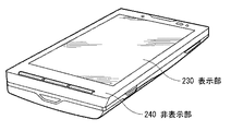
図40は、上記実施の形態の表示装置が適用されるスマートフォンの外観を表したものである。このスマートフォンは、例えば、表示部230および非表示部240を有しており、この表示部230が上記実施の形態の表示装置により構成されている。上記実施の形態等の表示装置は、電流密度が小さく、低消費電力であるので、スマートフォンにも好適に用いられる。
(Application example 1)
FIG. 40 illustrates the appearance of a smartphone to which the display device of the above embodiment is applied. This smartphone has, for example, a display unit 230 and a non-display unit 240, and the display unit 230 is configured by the display device of the above embodiment. Since the display devices of the above-described embodiments and the like have a low current density and low power consumption, they are preferably used for smartphones.
(適用例2)
図41は、上記実施の形態の表示装置が適用されるテレビジョン装置の外観を表したものである。このテレビジョン装置は、例えば、フロントパネル310およびフィルターガラス320を含む映像表示画面部300を有しており、この映像表示画面部300は、上記実施の形態の表示装置により構成されている。上記実施の形態等の表示装置は、高精細化が可能であるので、テレビジョン装置にも好適に用いられる。
(Application example 2)
FIG. 41 illustrates an appearance of a television device to which the display device of the above embodiment is applied. This television apparatus has, for example, a video display screen unit 300 including a front panel 310 and a
以上、実施の形態および変形例を挙げて本技術を説明したが、本技術は上記実施の形態等に限定されるものではなく、種々変形が可能である。例えば、上記実施の形態等において説明した各層の材料および厚み、または成膜方法および成膜条件等は限定されるものではなく、他の材料および厚みとしてもよく、または他の成膜方法および成膜条件としてもよい。 Although the present technology has been described with the embodiment and the modification, the present technology is not limited to the above-described embodiment and the like, and various modifications can be made. For example, the material and thickness of each layer described in the above embodiment and the like, or the film formation method and film formation conditions are not limited, and other materials and thicknesses may be used. It is good also as film | membrane conditions.
また、上記実施の形態等においては、発光層として赤色発光層,緑色発光層および青色発光層の3層を含む白色発光用の発光層を形成した場合について説明したが、白色発光用の発光層の構成は特に限定されず、橙色発光層および青色発光層、あるいは、青緑色発光層および赤色発光層など、互いに補色関係にある2色の発光層を積層した構造としてもよい。更に、上記実施の形態等では、機能層として有機層を用いる場合について説明したが、発光層を含む無機層を用いるようにしてもよい。 In the above-described embodiment and the like, the case where the light emitting layer for white light emission including the red light emitting layer, the green light emitting layer, and the blue light emitting layer is formed as the light emitting layer has been described. The structure of is not particularly limited, and may be a structure in which two light emitting layers having complementary colors such as an orange light emitting layer and a blue light emitting layer, or a blue green light emitting layer and a red light emitting layer are stacked. Furthermore, although the case where an organic layer is used as a functional layer has been described in the above embodiment and the like, an inorganic layer including a light emitting layer may be used.
更に、上記実施の形態等では、第1電極21を陽極、第2電極23を陰極とする場合について説明したが、陽極および陰極を逆にして、第1電極21を陰極、第2電極23を陽極としてもよい。
Further, in the above-described embodiment, the case where the
加えて、上記実施の形態等では、赤(R),緑(G),青(B)の3つのサブピクセルにより表示装置を構成する場合を例示したが、サブピクセルの構成はどのようなものであってもよく、例えば赤(R),緑(G),青(B),白(W)の4つのサブピクセルにより表示装置を構成するようにしてもよい。 In addition, in the above-described embodiment and the like, the case where the display device is configured by three sub-pixels of red (R), green (G), and blue (B) is illustrated, but what is the configuration of the sub-pixels? For example, the display device may be configured by four sub-pixels of red (R), green (G), blue (B), and white (W).
更にまた、上記実施の形態等では、カラーフィルタ32を設ける場合について説明したが、カラーフィルタを設けずに表示装置を構成するようにしてもよい。例えば、サブピクセル毎に赤色発光層,緑色発光層,青色発光層を塗り分ける場合や、白黒表示を行う場合には、カラーフィルタを省略してもよい。
Furthermore, although the case where the
なお、本明細書に記載された効果はあくまで例示であってこれに限定されるものではなく、また他の効果があってもよい。 In addition, the effect described in this specification is an illustration to the last, and is not limited to this, There may exist another effect.
なお、本技術は以下のような構成も取ることができる。
(1)駆動配線と、前記駆動配線を覆うとともに、接続孔を有する平坦化層と、前記平坦化層上に設けられ、前記接続孔を介して前記駆動配線に電気的に接続された中継電極と、絶縁材料からなり、前記接続孔に設けられた穴埋め部材と、前記穴埋め部材と同一材料により構成されるとともに、前記中継電極の端部を覆う第1隔壁と、前記穴埋め部材を覆い、前記中継電極に電気的に接続された第1電極と、前記第1電極に対向する第2電極と、前記第1電極と前記第2電極との間の発光層を含む機能層とを備えた表示装置。
(2)前記穴埋め部材は前記接続孔を塞いでいる前記(1)に記載の表示装置。
(3)前記第1隔壁は、前記第1電極の端部も覆っている前記(1)または(2)に記載の表示装置。
(4)前記第1電極は、平面視で前記中継電極よりも広い領域にわたって延在している前記(1)乃至(3)のうちいずれか1つに記載の表示装置。
(5)前記第1電極は、前記第1隔壁の側面を覆っている前記(1)に記載の表示装置。
(6)前記第1電極の端部を覆う第2隔壁を有する前記(5)に記載の表示装置。
(7)前記第1隔壁の側面に第1反射部材を有する前記(1)乃至(6)のうちいずれか1つに記載の表示装置。
(8)前記穴埋め部材と同一材料により構成されるとともに、前記中継電極の一部を覆う第3隔壁を有する前記(1)に記載の表示装置。
(9)前記第1電極は前記第3隔壁を覆っている前記(8)に記載の表示装置。
(10)複数の前記第3隔壁が、互いに間隙を有するように設けられている。前記(8)または(9)に記載の表示装置。
(11)前記第3隔壁の側面に第2反射部材を有する前記(8)乃至(10)のうちいずれか1つに記載の表示装置。
(12)前記第1電極は光反射性材料を含み、前記第2電極は光透過性材料を含んでいる前記(1)乃至(11)のうちいずれか1つに記載の表示装置。
(13)前記中継電極は光反射性材料を含み、前記第1電極および前記第2電極は光透過性材料を含んでいる前記(1)乃至(11)のうちいずれか1つに記載の表示装置。
(14)前記駆動配線、前記中継電極および前記第1電極は光透過性材料を含み、前記第2電極は光反射性材料を含んでいる前記(1)乃至(11)のうちいずれか1つに記載の表示装置。
(15)一つの前記中継電極が、複数の前記接続孔で前記駆動配線に電気的に接続されている前記(1)乃至(14)のうちいずれか1つに記載の表示装置。
(16)前記第1電極の厚みは、前記中継電極の厚みよりも小さい前記(1)乃至(15)のうちいずれか1つに記載の表示装置。
(17)前記穴埋め部材と前記第1隔壁とが接している前記(1)乃至(16)のうちいずれか1つに記載の表示装置。
(18)前記機能層は有機層である前記(1)乃至(17)のうちいずれか1つに記載の表示装置。
(19)表示装置を備え、前記表示装置は、駆動配線と、前記駆動配線を覆うとともに、接続孔を有する平坦化層と、前記平坦化層上に設けられ、前記接続孔を介して前記駆動配線に電気的に接続された中継電極と、絶縁材料からなり、前記接続孔に設けられた穴埋め部材と、前記穴埋め部材と同一材料により構成されるとともに、前記中継電極の端部を覆う第1隔壁と、前記穴埋め部材を覆い、前記中継電極に電気的に接続された第1電極と、前記第1電極に対向する第2電極と、前記第1電極と前記第2電極との間の発光層を含む機能層とを含む電子機器。
(20)駆動配線を形成することと、前記駆動配線を覆う平坦化層を成膜した後、前記平坦化層に接続孔を形成することと、前記平坦化層上に中継電極を形成するとともに、前記接続孔を介して前記中継電極を前記駆動配線に電気的に接続することと、前記接続孔に、絶縁材料からなる穴埋め部材を形成するととともに、前記中継電極の端部を覆う第1隔壁を、前記穴埋め部材と同一材料を用いて形成することと、前記穴埋め部材を覆うように第1電極を形成するとともに、前記第1電極を前記中継電極に電気的に接続することと、前記第1電極上に、発光層を含む機能層および第2電極をこの順に形成することとを含む表示装置の製造方法。
In addition, this technique can also take the following structures.
(1) A drive wiring, a planarization layer that covers the drive wiring and has a connection hole, and a relay electrode that is provided on the planarization layer and is electrically connected to the drive wiring through the connection hole And made of an insulating material, the hole filling member provided in the connection hole, the same material as the hole filling member, a first partition wall covering the end of the relay electrode, and covering the hole filling member, A display comprising a first electrode electrically connected to the relay electrode, a second electrode facing the first electrode, and a functional layer including a light emitting layer between the first electrode and the second electrode apparatus.
(2) The display device according to (1), wherein the hole filling member closes the connection hole.
(3) The display device according to (1) or (2), wherein the first partition wall also covers an end portion of the first electrode.
(4) The display device according to any one of (1) to (3), wherein the first electrode extends over a wider area than the relay electrode in plan view.
(5) The display device according to (1), wherein the first electrode covers a side surface of the first partition.
(6) The display device according to (5), further including a second partition wall that covers an end portion of the first electrode.
(7) The display device according to any one of (1) to (6), wherein a first reflecting member is provided on a side surface of the first partition.
(8) The display device according to (1), including a third partition wall made of the same material as the hole filling member and covering a part of the relay electrode.
(9) The display device according to (8), wherein the first electrode covers the third partition.
(10) The plurality of third partition walls are provided so as to have a gap therebetween. The display device according to (8) or (9).
(11) The display device according to any one of (8) to (10), wherein a second reflecting member is provided on a side surface of the third partition wall.
(12) The display device according to any one of (1) to (11), wherein the first electrode includes a light reflective material and the second electrode includes a light transmissive material.
(13) The display according to any one of (1) to (11), wherein the relay electrode includes a light reflective material, and the first electrode and the second electrode include a light transmissive material. apparatus.
(14) The drive wiring, the relay electrode, and the first electrode include a light transmissive material, and the second electrode includes a light reflective material, and any one of (1) to (11) The display device described in 1.
(15) The display device according to any one of (1) to (14), wherein one relay electrode is electrically connected to the drive wiring through a plurality of connection holes.
(16) The display device according to any one of (1) to (15), wherein a thickness of the first electrode is smaller than a thickness of the relay electrode.
(17) The display device according to any one of (1) to (16), wherein the hole-filling member and the first partition wall are in contact with each other.
(18) The display device according to any one of (1) to (17), wherein the functional layer is an organic layer.
(19) A display device is provided, and the display device covers the drive wiring, the planarization layer that covers the drive wiring and has a connection hole, and is provided on the planarization layer, and the drive through the connection hole. A relay electrode that is electrically connected to the wiring, an insulating material, a hole filling member provided in the connection hole, and a first material that is made of the same material as the hole filling member and covers an end of the relay electrode A partition, a first electrode that covers the hole filling member and is electrically connected to the relay electrode, a second electrode facing the first electrode, and light emission between the first electrode and the second electrode An electronic device including a functional layer including a layer.
(20) After forming the drive wiring, forming a planarization layer covering the drive wiring, forming a connection hole in the planarization layer, and forming a relay electrode on the planarization layer Electrically connecting the relay electrode to the drive wiring through the connection hole; forming a filling member made of an insulating material in the connection hole; and covering the end of the relay electrode Using the same material as the hole-filling member, forming a first electrode so as to cover the hole-filling member, and electrically connecting the first electrode to the relay electrode; A method of manufacturing a display device, comprising: forming a functional layer including a light emitting layer and a second electrode in this order on one electrode.
1,1A,1B,1C,1D,1E,2,2A,3,3A,4・・・表示装置、10・・・有機発光素子、10R・・・赤色有機発光素子、10G・・・緑色有機発光素子、11・・・基板、12・・・TFT層、13・・・平坦化層、H1・・・接続孔、14・・・中継電極、15・・・穴埋め部材、21,21A,21B・・・第1電極、22・・・有機層、23・・・第2電極、24,27,28・・・隔壁、25・・・封止層、26・・・反射部材、31・・・封止基板、32・・・カラーフィルタ、33・・・遮光層、34・・・オーバーコート層。 1, 1A, 1B, 1C, 1D, 1E, 2, 2A, 3, 3A, 4 ... display device, 10 ... organic light emitting element, 10R ... red organic light emitting element, 10G ... green organic Light emitting element, 11 ... substrate, 12 ... TFT layer, 13 ... flattening layer, H1 ... connection hole, 14 ... relay electrode, 15 ... hole filling member, 21, 21A, 21B ... 1st electrode, 22 ... Organic layer, 23 ... 2nd electrode, 24, 27, 28 ... Partition, 25 ... Sealing layer, 26 ... Reflective member, 31 ... -Sealing substrate, 32 ... color filter, 33 ... light shielding layer, 34 ... overcoat layer.
Claims (21)
前記駆動配線を覆うとともに、接続孔を有する平坦化層と、
前記平坦化層上に設けられ、前記接続孔を介して前記駆動配線に電気的に接続された中継電極と、
絶縁材料からなるとともに、前記接続孔および前記接続孔の近傍に設けられ、前記平坦化層上の前記中継電極にかかる穴埋め部材と、
前記穴埋め部材と同一材料により構成されるとともに、前記中継電極の端部を覆う第1隔壁と、
前記穴埋め部材を覆い、前記中継電極に電気的に接続された第1電極と、
前記第1電極に対向する第2電極と、
前記第1電極と前記第2電極との間の発光層を含む機能層と
を備えた表示装置。 Drive wiring,
A flattening layer covering the drive wiring and having a connection hole;
A relay electrode provided on the planarization layer and electrically connected to the drive wiring through the connection hole;
Rutotomoni such an insulating material, provided in the vicinity of the connecting hole and the connecting hole, the filling member according to the relay electrode on the planarization layer,
A first partition wall made of the same material as the hole filling member and covering an end of the relay electrode;
A first electrode covering the hole filling member and electrically connected to the relay electrode;
A second electrode facing the first electrode;
A display device comprising: a functional layer including a light emitting layer between the first electrode and the second electrode.
請求項1に記載の表示装置。 The display device according to claim 1, wherein the hole filling member closes the connection hole.
請求項1または2に記載の表示装置。 It said first septum display device according to claim 1 or 2 also covers the end portion of the first electrode.
請求項1乃至3のうちいずれか1つに記載の表示装置。 The first electrode A display device according to any one of claims 1 to 3 which extends over a wider area than the relay electrode in a plan view.
請求項1に記載の表示装置。 The display device according to claim 1, wherein the first electrode covers a side surface of the first partition.
請求項5に記載の表示装置。 The display device according to claim 5, further comprising a second partition wall that covers an end portion of the first electrode.
請求項1乃至3のうちいずれか1つに記載の表示装置。 Display device according to any one of claims 1 to 3 having a first reflecting member on a side surface of the first partition wall.
請求項1乃至3のうちいずれか1つに記載の表示装置。 Wherein together it is constituted by a filling member of the same material, the display device according to any one of claims 1 to 3 having a third partition covering a portion of the relay electrode.
請求項8に記載の表示装置。 The display device according to claim 8, wherein the first electrode covers the third partition wall.
請求項8または9に記載の表示装置。 The plurality of third partition walls are provided so as to have a gap therebetween.
The display device according to claim 8 or 9 .
請求項8乃至10のうちいずれか1つに記載の表示装置。 Display device according to any one of claims 8 to 10 having a second reflecting member on a side of the third partition.
前記第2電極は光透過性材料を含んでいる
請求項1乃至11のうちいずれか1つに記載の表示装置。 The first electrode includes a light reflective material;
Display device according to any one of claims 1 to 11 wherein the second electrode includes a light-transmissive material.
請求項1乃至11のうちいずれか1つに記載の表示装置。 The relay electrode comprises a light reflective material, the display device according to any one of the first electrode and the second electrode according to claim 1 to 11 includes a light transmissive material.
前記第2電極は光反射性材料を含んでいる
請求項1乃至11のうちいずれか1つに記載の表示装置。 The drive wiring, the relay electrode, and the first electrode include a light transmissive material,
Display device according to any one of claims 1 to 11 wherein the second electrode includes a light reflective material.
請求項1乃至14のうちいずれか1つに記載の表示装置。 One of the relay electrodes, the display device according to any one of claims 1 to 14 is electrically connected to the drive wiring in a plurality of said connection hole.
請求項1乃至15のうちいずれか1つに記載の表示装置。 The thickness of the first electrode, a display device according to any one of smaller claims 1 to 15 than the thickness of the relay electrode.
請求項1乃至3のうちいずれか1つに記載の表示装置。 The display device according to claim 1, wherein the hole filling member and the first partition wall are in contact with each other .
請求項1乃至17のうちいずれか1つに記載の表示装置。 Display device according to any one of claims 1 to 17 wherein the functional layer is an organic layer.
請求項1乃至18のうちいずれか1つに記載の表示装置。The display device according to claim 1.
前記表示装置は、
駆動配線と、
前記駆動配線を覆うとともに、接続孔を有する平坦化層と、
前記平坦化層上に設けられ、前記接続孔を介して前記駆動配線に電気的に接続された中継電極と、
絶縁材料からなるとともに、前記接続孔および前記接続孔の近傍に設けられ、前記平坦化層上の前記中継電極にかかる穴埋め部材と、
前記穴埋め部材と同一材料により構成されるとともに、前記中継電極の端部を覆う第1隔壁と、
前記穴埋め部材を覆い、前記中継電極に電気的に接続された第1電極と、
前記第1電極に対向する第2電極と、
前記第1電極と前記第2電極との間の発光層を含む機能層とを含む
電子機器。 A display device,
The display device
Drive wiring,
A flattening layer covering the drive wiring and having a connection hole;
A relay electrode provided on the planarization layer and electrically connected to the drive wiring through the connection hole;
Rutotomoni such an insulating material, provided in the vicinity of the connecting hole and the connecting hole, the filling member according to the relay electrode on the planarization layer,
A first partition wall made of the same material as the hole filling member and covering an end of the relay electrode;
A first electrode covering the hole filling member and electrically connected to the relay electrode;
A second electrode facing the first electrode;
An electronic device including a functional layer including a light emitting layer between the first electrode and the second electrode.
前記駆動配線を覆う平坦化層を成膜した後、前記平坦化層に接続孔を形成することと、
前記平坦化層上に中継電極を形成するとともに、前記接続孔を介して前記中継電極を前記駆動配線に電気的に接続することと、
前記平坦化層上の前記中継電極にかかるように、前記接続孔および前記接続孔の近傍に、絶縁材料からなる穴埋め部材を形成するととともに、前記中継電極の端部を覆う第1隔壁を、前記穴埋め部材と同一材料を用いて形成することと、
前記穴埋め部材を覆うように第1電極を形成するとともに、前記第1電極を前記中継電極に電気的に接続することと、
前記第1電極上に、発光層を含む機能層および第2電極をこの順に形成することと
を含む表示装置の製造方法。 Forming the drive wiring;
After forming a planarization layer covering the drive wiring, forming a connection hole in the planarization layer;
Forming a relay electrode on the planarizing layer and electrically connecting the relay electrode to the drive wiring through the connection hole;
Forming a filling member made of an insulating material in the vicinity of the connection hole and the connection hole so as to cover the relay electrode on the planarizing layer, and a first partition wall covering an end of the relay electrode, Forming using the same material as the hole filling member;
Forming a first electrode so as to cover the hole filling member, and electrically connecting the first electrode to the relay electrode;
Forming a functional layer including a light emitting layer and a second electrode in this order on the first electrode.
Priority Applications (4)
| Application Number | Priority Date | Filing Date | Title |
|---|---|---|---|
| JP2014021603A JP6160499B2 (en) | 2014-02-06 | 2014-02-06 | Display device, display device manufacturing method, and electronic apparatus |
| US14/603,816 US10109693B2 (en) | 2014-02-06 | 2015-01-23 | Display unit, method of manufacturing display unit, and electronic apparatus |
| US16/133,014 US11222937B2 (en) | 2014-02-06 | 2018-09-17 | Display unit with light emitting layer between first and second electrodes |
| US17/551,465 US11778869B2 (en) | 2014-02-06 | 2021-12-15 | Display unit and electronic apparatus including functional layer with light-emitting layer and hole injection layer |
Applications Claiming Priority (1)
| Application Number | Priority Date | Filing Date | Title |
|---|---|---|---|
| JP2014021603A JP6160499B2 (en) | 2014-02-06 | 2014-02-06 | Display device, display device manufacturing method, and electronic apparatus |
Publications (3)
| Publication Number | Publication Date |
|---|---|
| JP2015149194A JP2015149194A (en) | 2015-08-20 |
| JP2015149194A5 JP2015149194A5 (en) | 2016-03-17 |
| JP6160499B2 true JP6160499B2 (en) | 2017-07-12 |
Family
ID=53755563
Family Applications (1)
| Application Number | Title | Priority Date | Filing Date |
|---|---|---|---|
| JP2014021603A Active JP6160499B2 (en) | 2014-02-06 | 2014-02-06 | Display device, display device manufacturing method, and electronic apparatus |
Country Status (2)
| Country | Link |
|---|---|
| US (3) | US10109693B2 (en) |
| JP (1) | JP6160499B2 (en) |
Families Citing this family (19)
| Publication number | Priority date | Publication date | Assignee | Title |
|---|---|---|---|---|
| TWI674671B (en) * | 2013-05-28 | 2019-10-11 | 日商新力股份有限公司 | Display device and electronic device |
| KR101818423B1 (en) | 2015-09-23 | 2018-01-16 | 엘지디스플레이 주식회사 | Organic Light Emitting Diode Display Device |
| KR102516054B1 (en) * | 2015-11-13 | 2023-03-31 | 삼성디스플레이 주식회사 | Organic light emitting display apparatus and method for manufacturing the same |
| JP2017111926A (en) * | 2015-12-15 | 2017-06-22 | 株式会社ジャパンディスプレイ | Organic electroluminescent display device |
| JP2017152252A (en) * | 2016-02-25 | 2017-08-31 | 株式会社ジャパンディスプレイ | Display device |
| US10069098B2 (en) * | 2016-06-29 | 2018-09-04 | Lg Display Co., Ltd. | Organic light emitting display device, method of manufacturing the same, and head mounted display including the same |
| KR20180002471A (en) * | 2016-06-29 | 2018-01-08 | 엘지디스플레이 주식회사 | Organic light emitting display device, method for manufacturing the same, and head mounted display including the same |
| US11038140B2 (en) | 2017-02-13 | 2021-06-15 | Sony Corporation | Display device, electronic device, and method of producing display device |
| WO2018147050A1 (en) | 2017-02-13 | 2018-08-16 | ソニー株式会社 | Display device and electronic apparatus |
| CN107482130B (en) * | 2017-08-02 | 2020-05-26 | 京东方科技集团股份有限公司 | Organic light-emitting panel, method for manufacturing same, and organic light-emitting device |
| GB2567421B (en) * | 2017-10-03 | 2022-09-28 | Flexenable Ltd | Photo-active devices |
| JP7212036B2 (en) * | 2018-03-30 | 2023-01-24 | ソニーセミコンダクタソリューションズ株式会社 | DISPLAY DEVICE, METHOD FOR MANUFACTURING DISPLAY DEVICE, AND ELECTRONIC DEVICE |
| KR102611997B1 (en) * | 2018-06-29 | 2023-12-07 | 엘지디스플레이 주식회사 | Display device |
| KR102532111B1 (en) * | 2018-07-23 | 2023-05-11 | 엘지디스플레이 주식회사 | Lighting apparatus using organic light emitting diode |
| US20200235180A1 (en) * | 2019-01-18 | 2020-07-23 | Samsung Display Co., Ltd. | Display panel |
| CN109873023B (en) * | 2019-03-29 | 2021-10-19 | 京东方科技集团股份有限公司 | OLED display substrate, preparation method thereof and display device |
| TWI699903B (en) * | 2019-05-17 | 2020-07-21 | 友達光電股份有限公司 | Display panel and fabrication method thereof |
| KR20210082908A (en) * | 2019-12-26 | 2021-07-06 | 엘지디스플레이 주식회사 | Electroluminescent Display Device |
| WO2023276295A1 (en) * | 2021-06-28 | 2023-01-05 | ソニーグループ株式会社 | Semiconductor device and display apparatus |
Family Cites Families (16)
| Publication number | Priority date | Publication date | Assignee | Title |
|---|---|---|---|---|
| JP3332773B2 (en) * | 1996-03-15 | 2002-10-07 | シャープ株式会社 | Active matrix substrate and method of manufacturing active matrix substrate |
| JP2001148291A (en) | 1999-11-19 | 2001-05-29 | Sony Corp | Display device and its manufacturing method |
| TW525305B (en) * | 2000-02-22 | 2003-03-21 | Semiconductor Energy Lab | Self-light-emitting device and method of manufacturing the same |
| JP4925528B2 (en) * | 2000-09-29 | 2012-04-25 | 三洋電機株式会社 | Display device |
| JP4693253B2 (en) * | 2001-01-30 | 2011-06-01 | 株式会社半導体エネルギー研究所 | Light emitting device, electronic equipment |
| JP3608614B2 (en) * | 2001-03-28 | 2005-01-12 | 株式会社日立製作所 | Display device |
| US6815723B2 (en) * | 2001-12-28 | 2004-11-09 | Semiconductor Energy Laboratory Co., Ltd. | Light emitting device, method of manufacturing the same, and manufacturing apparatus therefor |
| WO2005039248A1 (en) * | 2003-09-19 | 2005-04-28 | Sony Corporation | Display device, manufacturing method thereof, organic light emitting device, and manufacturing method thereof |
| US7893438B2 (en) * | 2003-10-16 | 2011-02-22 | Samsung Mobile Display Co., Ltd. | Organic light-emitting display device including a planarization pattern and method for manufacturing the same |
| JP2007165214A (en) * | 2005-12-16 | 2007-06-28 | Seiko Epson Corp | Electroluminescent device and electronic apparatus |
| JP2008130363A (en) * | 2006-11-21 | 2008-06-05 | Fuji Electric Holdings Co Ltd | Organic el element, its manufacturing method, organic el display, and its manufacturing method |
| KR101218844B1 (en) * | 2009-08-31 | 2013-01-21 | 파나소닉 주식회사 | Light emitting element and method for manufacturing the same, and light emitting apparatus |
| KR101113394B1 (en) * | 2009-12-17 | 2012-02-29 | 삼성모바일디스플레이주식회사 | array substrate of liquid crystal display |
| WO2011077477A1 (en) * | 2009-12-22 | 2011-06-30 | パナソニック株式会社 | Display device and method for manufacturing same |
| JP5612691B2 (en) * | 2010-08-06 | 2014-10-22 | パナソニック株式会社 | Organic EL device and method for manufacturing the same |
| JP6104099B2 (en) * | 2013-08-21 | 2017-03-29 | 株式会社ジャパンディスプレイ | Organic EL display device |
-
2014
- 2014-02-06 JP JP2014021603A patent/JP6160499B2/en active Active
-
2015
- 2015-01-23 US US14/603,816 patent/US10109693B2/en active Active
-
2018
- 2018-09-17 US US16/133,014 patent/US11222937B2/en active Active
-
2021
- 2021-12-15 US US17/551,465 patent/US11778869B2/en active Active
Also Published As
| Publication number | Publication date |
|---|---|
| US10109693B2 (en) | 2018-10-23 |
| US20220181415A1 (en) | 2022-06-09 |
| US20150221893A1 (en) | 2015-08-06 |
| US11778869B2 (en) | 2023-10-03 |
| JP2015149194A (en) | 2015-08-20 |
| US20190096972A1 (en) | 2019-03-28 |
| US11222937B2 (en) | 2022-01-11 |
Similar Documents
| Publication | Publication Date | Title |
|---|---|---|
| JP6160499B2 (en) | Display device, display device manufacturing method, and electronic apparatus | |
| KR102481551B1 (en) | Display unit, method of manufacturing display unit, and electronic apparatus | |
| JP6111461B2 (en) | Display device and electronic device | |
| US9147860B2 (en) | Light emitting device, method of manufacturing the light emitting device, and display unit | |
| KR102166341B1 (en) | Organic Light Emitting Diode Display Having High Aperture Ratio And Method For Manufacturing The Same | |
| CN112071882A (en) | Display substrate, preparation method thereof and display device | |
| JP2018097361A (en) | Organic light emitting diode display and method of manufacturing the same | |
| EP3021363B1 (en) | Organic light-emitting diode display having high aperture ratio and method for manufacturing the same | |
| KR102108577B1 (en) | Light-emitting element and display device | |
| JP2015069844A (en) | Display device and electronic apparatus | |
| US10707446B2 (en) | Display unit and electronic apparatus | |
| US9059124B2 (en) | Display device and method for manufacturing display device | |
| JP6159946B2 (en) | Display device and electronic device | |
| JP2015022914A (en) | Display device and method for manufacturing the same, and electronic apparatus | |
| KR102618593B1 (en) | Organic light emitting display and method of fabricating the same | |
| KR20130093187A (en) | Organic light emitting display device and method for manufacturing thereof | |
| KR20150040249A (en) | Light emitting device, display unit including the same, and electronic apparatus | |
| KR101820166B1 (en) | White organic light emitting diode display device and method of fabricating the same | |
| KR101622563B1 (en) | Top emission type organic Electroluminescent Device | |
| KR102053440B1 (en) | Organic Light Emitting Diode Display Having High Aperture Ratio And Method For Manufacturing The Same | |
| KR102247825B1 (en) | Bottom Emission Type Organic Light Emission Diode Display Having Color Filters And Method For Manufacturing The Same | |
| KR102355605B1 (en) | Organic Light Emitting Diode Display Device and Method of Fabricating the Same | |
| JP6281135B2 (en) | Display device and electronic device | |
| KR20190077673A (en) | Organic light emitting display device | |
| JP2019129221A (en) | Display device and method for manufacturing the same |
Legal Events
| Date | Code | Title | Description |
|---|---|---|---|
| A521 | Request for written amendment filed |
Free format text: JAPANESE INTERMEDIATE CODE: A523 Effective date: 20160202 |
|
| A621 | Written request for application examination |
Free format text: JAPANESE INTERMEDIATE CODE: A621 Effective date: 20160202 |
|
| A977 | Report on retrieval |
Free format text: JAPANESE INTERMEDIATE CODE: A971007 Effective date: 20161011 |
|
| A131 | Notification of reasons for refusal |
Free format text: JAPANESE INTERMEDIATE CODE: A131 Effective date: 20161018 |
|
| A521 | Request for written amendment filed |
Free format text: JAPANESE INTERMEDIATE CODE: A523 Effective date: 20161208 |
|
| TRDD | Decision of grant or rejection written | ||
| A01 | Written decision to grant a patent or to grant a registration (utility model) |
Free format text: JAPANESE INTERMEDIATE CODE: A01 Effective date: 20170516 |
|
| A61 | First payment of annual fees (during grant procedure) |
Free format text: JAPANESE INTERMEDIATE CODE: A61 Effective date: 20170529 |
|
| R151 | Written notification of patent or utility model registration |
Ref document number: 6160499 Country of ref document: JP Free format text: JAPANESE INTERMEDIATE CODE: R151 |
|
| R250 | Receipt of annual fees |
Free format text: JAPANESE INTERMEDIATE CODE: R250 |