JP2013151720A - Vacuum film forming apparatus - Google Patents
Vacuum film forming apparatus Download PDFInfo
- Publication number
- JP2013151720A JP2013151720A JP2012012749A JP2012012749A JP2013151720A JP 2013151720 A JP2013151720 A JP 2013151720A JP 2012012749 A JP2012012749 A JP 2012012749A JP 2012012749 A JP2012012749 A JP 2012012749A JP 2013151720 A JP2013151720 A JP 2013151720A
- Authority
- JP
- Japan
- Prior art keywords
- substrate
- stage
- gas
- vacuum
- vacuum chamber
- Prior art date
- Legal status (The legal status is an assumption and is not a legal conclusion. Google has not performed a legal analysis and makes no representation as to the accuracy of the status listed.)
- Pending
Links
Images


Classifications
-
- C—CHEMISTRY; METALLURGY
- C23—COATING METALLIC MATERIAL; COATING MATERIAL WITH METALLIC MATERIAL; CHEMICAL SURFACE TREATMENT; DIFFUSION TREATMENT OF METALLIC MATERIAL; COATING BY VACUUM EVAPORATION, BY SPUTTERING, BY ION IMPLANTATION OR BY CHEMICAL VAPOUR DEPOSITION, IN GENERAL; INHIBITING CORROSION OF METALLIC MATERIAL OR INCRUSTATION IN GENERAL
- C23C—COATING METALLIC MATERIAL; COATING MATERIAL WITH METALLIC MATERIAL; SURFACE TREATMENT OF METALLIC MATERIAL BY DIFFUSION INTO THE SURFACE, BY CHEMICAL CONVERSION OR SUBSTITUTION; COATING BY VACUUM EVAPORATION, BY SPUTTERING, BY ION IMPLANTATION OR BY CHEMICAL VAPOUR DEPOSITION, IN GENERAL
- C23C16/00—Chemical coating by decomposition of gaseous compounds, without leaving reaction products of surface material in the coating, i.e. chemical vapour deposition [CVD] processes
- C23C16/44—Chemical coating by decomposition of gaseous compounds, without leaving reaction products of surface material in the coating, i.e. chemical vapour deposition [CVD] processes characterised by the method of coating
- C23C16/455—Chemical coating by decomposition of gaseous compounds, without leaving reaction products of surface material in the coating, i.e. chemical vapour deposition [CVD] processes characterised by the method of coating characterised by the method used for introducing gases into reaction chamber or for modifying gas flows in reaction chamber
- C23C16/45563—Gas nozzles
-
- C—CHEMISTRY; METALLURGY
- C23—COATING METALLIC MATERIAL; COATING MATERIAL WITH METALLIC MATERIAL; CHEMICAL SURFACE TREATMENT; DIFFUSION TREATMENT OF METALLIC MATERIAL; COATING BY VACUUM EVAPORATION, BY SPUTTERING, BY ION IMPLANTATION OR BY CHEMICAL VAPOUR DEPOSITION, IN GENERAL; INHIBITING CORROSION OF METALLIC MATERIAL OR INCRUSTATION IN GENERAL
- C23C—COATING METALLIC MATERIAL; COATING MATERIAL WITH METALLIC MATERIAL; SURFACE TREATMENT OF METALLIC MATERIAL BY DIFFUSION INTO THE SURFACE, BY CHEMICAL CONVERSION OR SUBSTITUTION; COATING BY VACUUM EVAPORATION, BY SPUTTERING, BY ION IMPLANTATION OR BY CHEMICAL VAPOUR DEPOSITION, IN GENERAL
- C23C16/00—Chemical coating by decomposition of gaseous compounds, without leaving reaction products of surface material in the coating, i.e. chemical vapour deposition [CVD] processes
- C23C16/44—Chemical coating by decomposition of gaseous compounds, without leaving reaction products of surface material in the coating, i.e. chemical vapour deposition [CVD] processes characterised by the method of coating
- C23C16/4412—Details relating to the exhausts, e.g. pumps, filters, scrubbers, particle traps
-
- C—CHEMISTRY; METALLURGY
- C23—COATING METALLIC MATERIAL; COATING MATERIAL WITH METALLIC MATERIAL; CHEMICAL SURFACE TREATMENT; DIFFUSION TREATMENT OF METALLIC MATERIAL; COATING BY VACUUM EVAPORATION, BY SPUTTERING, BY ION IMPLANTATION OR BY CHEMICAL VAPOUR DEPOSITION, IN GENERAL; INHIBITING CORROSION OF METALLIC MATERIAL OR INCRUSTATION IN GENERAL
- C23C—COATING METALLIC MATERIAL; COATING MATERIAL WITH METALLIC MATERIAL; SURFACE TREATMENT OF METALLIC MATERIAL BY DIFFUSION INTO THE SURFACE, BY CHEMICAL CONVERSION OR SUBSTITUTION; COATING BY VACUUM EVAPORATION, BY SPUTTERING, BY ION IMPLANTATION OR BY CHEMICAL VAPOUR DEPOSITION, IN GENERAL
- C23C16/00—Chemical coating by decomposition of gaseous compounds, without leaving reaction products of surface material in the coating, i.e. chemical vapour deposition [CVD] processes
- C23C16/44—Chemical coating by decomposition of gaseous compounds, without leaving reaction products of surface material in the coating, i.e. chemical vapour deposition [CVD] processes characterised by the method of coating
- C23C16/455—Chemical coating by decomposition of gaseous compounds, without leaving reaction products of surface material in the coating, i.e. chemical vapour deposition [CVD] processes characterised by the method of coating characterised by the method used for introducing gases into reaction chamber or for modifying gas flows in reaction chamber
- C23C16/45523—Pulsed gas flow or change of composition over time
- C23C16/45525—Atomic layer deposition [ALD]
- C23C16/45544—Atomic layer deposition [ALD] characterized by the apparatus
-
- C—CHEMISTRY; METALLURGY
- C23—COATING METALLIC MATERIAL; COATING MATERIAL WITH METALLIC MATERIAL; CHEMICAL SURFACE TREATMENT; DIFFUSION TREATMENT OF METALLIC MATERIAL; COATING BY VACUUM EVAPORATION, BY SPUTTERING, BY ION IMPLANTATION OR BY CHEMICAL VAPOUR DEPOSITION, IN GENERAL; INHIBITING CORROSION OF METALLIC MATERIAL OR INCRUSTATION IN GENERAL
- C23C—COATING METALLIC MATERIAL; COATING MATERIAL WITH METALLIC MATERIAL; SURFACE TREATMENT OF METALLIC MATERIAL BY DIFFUSION INTO THE SURFACE, BY CHEMICAL CONVERSION OR SUBSTITUTION; COATING BY VACUUM EVAPORATION, BY SPUTTERING, BY ION IMPLANTATION OR BY CHEMICAL VAPOUR DEPOSITION, IN GENERAL
- C23C16/00—Chemical coating by decomposition of gaseous compounds, without leaving reaction products of surface material in the coating, i.e. chemical vapour deposition [CVD] processes
- C23C16/44—Chemical coating by decomposition of gaseous compounds, without leaving reaction products of surface material in the coating, i.e. chemical vapour deposition [CVD] processes characterised by the method of coating
- C23C16/455—Chemical coating by decomposition of gaseous compounds, without leaving reaction products of surface material in the coating, i.e. chemical vapour deposition [CVD] processes characterised by the method of coating characterised by the method used for introducing gases into reaction chamber or for modifying gas flows in reaction chamber
- C23C16/45561—Gas plumbing upstream of the reaction chamber
-
- C—CHEMISTRY; METALLURGY
- C23—COATING METALLIC MATERIAL; COATING MATERIAL WITH METALLIC MATERIAL; CHEMICAL SURFACE TREATMENT; DIFFUSION TREATMENT OF METALLIC MATERIAL; COATING BY VACUUM EVAPORATION, BY SPUTTERING, BY ION IMPLANTATION OR BY CHEMICAL VAPOUR DEPOSITION, IN GENERAL; INHIBITING CORROSION OF METALLIC MATERIAL OR INCRUSTATION IN GENERAL
- C23C—COATING METALLIC MATERIAL; COATING MATERIAL WITH METALLIC MATERIAL; SURFACE TREATMENT OF METALLIC MATERIAL BY DIFFUSION INTO THE SURFACE, BY CHEMICAL CONVERSION OR SUBSTITUTION; COATING BY VACUUM EVAPORATION, BY SPUTTERING, BY ION IMPLANTATION OR BY CHEMICAL VAPOUR DEPOSITION, IN GENERAL
- C23C16/00—Chemical coating by decomposition of gaseous compounds, without leaving reaction products of surface material in the coating, i.e. chemical vapour deposition [CVD] processes
- C23C16/44—Chemical coating by decomposition of gaseous compounds, without leaving reaction products of surface material in the coating, i.e. chemical vapour deposition [CVD] processes characterised by the method of coating
- C23C16/54—Apparatus specially adapted for continuous coating
Landscapes
- Chemical & Material Sciences (AREA)
- General Chemical & Material Sciences (AREA)
- Chemical Kinetics & Catalysis (AREA)
- Engineering & Computer Science (AREA)
- Materials Engineering (AREA)
- Mechanical Engineering (AREA)
- Metallurgy (AREA)
- Organic Chemistry (AREA)
- Chemical Vapour Deposition (AREA)
Abstract
Description
本発明は、真空チャンバ内に配置された成膜対象たる基板に対して二種以上の原料ガスを交互に供給して化学反応により所定の薄膜を成膜する真空成膜装置に関する。 The present invention relates to a vacuum film forming apparatus for forming a predetermined thin film by a chemical reaction by alternately supplying two or more kinds of source gases to a substrate which is a film formation target disposed in a vacuum chamber.
半導体デバイスの製造工程においては、ウエハ等の成膜対象たる基板に所定の薄膜を成膜する成膜工程があり、この成膜工程に対しては、近年の半導体デバイスの微細化に伴い、低温度で成膜を実施することが要請されている。このことから、熱履歴の低減や良好な段差被覆性等の特徴を有するALD法を利用した成膜方法が注目されている。 In the manufacturing process of semiconductor devices, there is a film forming process for forming a predetermined thin film on a substrate to be formed such as a wafer. It is required to perform film formation at a temperature. For this reason, a film forming method using an ALD method having features such as reduction of thermal history and good step coverage is attracting attention.
上記成膜方法を実施する真空成膜装置は、例えば特許文献1で知られている。このものは、内部を加熱するヒータを有する真空チャンバを備える。真空チャンバの上部にはガス導入口が形成され、このガス導入口に切換弁を介して、ガス毎に設けられる複数の配管が夫々接続されている。また、真空チャンバ内の上部空間には、ガス導入口に連通するシャワーヘッドが設けられ、このシャワーヘッドに対向させて基板を保持するステージが設けられている。真空チャンバの底部には、内部のガスを排気するために真空ポンプに通じる排気口が形成されている。
A vacuum film forming apparatus that performs the film forming method is known, for example, from
そして、基板表面に第1原料ガスを供給し、この第1原料ガスを基板表面に化学吸着させて第1原料ガスの原子の層を形成する。次に、基板表面のガス雰囲気を不活性ガスにより置換した後、基板表面に第2反応ガスを供給し、基板表面に吸着されている第1反応ガスと反応させ、第2原料ガスの原子の層を形成する。次に、基板表面のガス雰囲気を不活性ガスにより更に置換した後、第1原料ガスを再度吸着し、上記同様、置換後に第2原料ガスを再度供給する。この一連の操作を繰り返し、二種以上の原料ガスを交互に供給して化学反応により所定の薄膜が成膜される。 Then, a first source gas is supplied to the substrate surface, and the first source gas is chemically adsorbed on the substrate surface to form an atomic layer of the first source gas. Next, after replacing the gas atmosphere on the substrate surface with an inert gas, a second reaction gas is supplied to the substrate surface to react with the first reaction gas adsorbed on the substrate surface, and the atoms of the second source gas Form a layer. Next, after the gas atmosphere on the substrate surface is further replaced with an inert gas, the first source gas is adsorbed again, and the second source gas is supplied again after the replacement in the same manner as described above. By repeating this series of operations, two or more kinds of source gases are alternately supplied to form a predetermined thin film by a chemical reaction.
然しながら、上記従来例の真空成膜装置では、基板表面、つまり、基板の成膜面に対して直交する方向から原料ガスを供給しているため、基板の成膜面全面に亘って原料ガスを効果的に吸着させることが困難であるという問題がある。そこで、基板の成膜面の一側から他側に向けてかつこの基板表面に沿って前記ガスを噴射するように原料ガスのガス供給手段を構成すると共に、この他側から真空チャンバ内に導入された原料ガス等を真空引きすることが考えられる。この場合、真空チャンバの側壁に、ガス供給手段としての切換弁や配管及び排気手段としての真空ポンプに通じる排気管等の部品をこの壁面から側方に延出させて設ける必要が生じ、装置の設置面積が大きくなるばかりか、場合によっては、これらの部品で制約されて中央の搬送室を備えたクラスターツール用の成膜モジュールとして利用できないという問題が生じ得る。 However, in the conventional vacuum film forming apparatus, since the source gas is supplied from the direction perpendicular to the substrate surface, that is, the film forming surface of the substrate, the material gas is supplied over the entire film forming surface of the substrate. There is a problem that it is difficult to adsorb effectively. Therefore, the gas supply means of the source gas is configured so as to inject the gas from one side of the film formation surface to the other side and along the surface of the substrate, and is introduced into the vacuum chamber from the other side. It is conceivable to evacuate the raw material gas and the like. In this case, it is necessary to provide parts such as a switching valve as a gas supply means and piping and an exhaust pipe leading to a vacuum pump as an exhaust means on the side wall of the vacuum chamber so as to extend laterally from the wall surface. In addition to an increase in the installation area, there may be a problem that, depending on the case, it is restricted by these components and cannot be used as a film forming module for a cluster tool having a central transfer chamber.
本発明は、以上の点に鑑み、基板の成膜面全面に亘って原料ガスを効果的に吸着させることができるという機能を損なうことなく、装置自体の設置面積の大型化を防止することができる真空成膜装置を提供することをその課題とする。 In view of the above, the present invention can prevent an increase in the installation area of the apparatus itself without impairing the function of effectively adsorbing the source gas over the entire film formation surface of the substrate. It is an object of the present invention to provide a vacuum film forming apparatus that can be used.
上記課題を解決するために、真空チャンバ内に配置された成膜対象たる基板に対して二種以上の原料ガスを交互に供給して化学反応により所定の薄膜を成膜する本発明の真空成膜装置は、真空チャンバ内で基板を保持するステージと、この基板に対しガスを交互に供給するガス供給手段と、真空チャンバ内のガスを排気する排気手段と、を備え、前記ステージで保持された前記基板の成膜面側を上とし、前記ガス供給手段は、ステージの一側に配置されて基板の一側から他側に向けてかつこの基板上面に沿って前記ガスのいずれかを噴射する少なくとも1個の噴射ノズルを有し、前記排気手段は、前記ステージの他側で真空チャンバの下壁に開設される排気口と、この真空チャンバの下方に設けられて排気口に連通する排気チャンバと、排気チャンバに接続されてこの排気チャンバ内を真空引きする真空ポンプとを有することを特徴とする。 In order to solve the above-described problems, the vacuum deposition of the present invention in which a predetermined thin film is formed by a chemical reaction by alternately supplying two or more kinds of source gases to a substrate to be deposited disposed in a vacuum chamber. The film apparatus includes a stage that holds the substrate in the vacuum chamber, a gas supply unit that alternately supplies gas to the substrate, and an exhaust unit that exhausts the gas in the vacuum chamber, and is held by the stage. The gas deposition means is disposed on one side of the stage and injects one of the gases from one side of the substrate toward the other side and along the upper surface of the substrate. And at least one injection nozzle configured to be provided on the lower side of the vacuum chamber on the other side of the stage and an exhaust port provided below the vacuum chamber and communicating with the exhaust port. Chamber and exhaust Connected to Yanba in and having a vacuum pump for evacuating the exhaust chamber.
本発明によれば、噴射ノズルにより、ステージの一側に配置されて基板の一側から他側に向けてかつこの基板上面に沿って所定のガスを供給すると共に、真空チャンバの圧力より低い圧力となる排気チャンバに通じる排気口をステージの他側に設けて基板を通過したガスが積極的に排気口を介して排気チャンバに排気されるため、基板の成膜面に亘って原料ガスを効果的に吸着させることができる。この場合、排気チャンバが真空チャンバの下方に設けられ、しかも、噴射ノズルを真空チャンバ内に配置して、この噴射ノズルに所定のガスを供給するガス供給管を真空チャンバの下方から接続することができる構成としたため、配管や排気管等の部品を真空チャンバの壁面から側方に延出させて設ける必要がなく、装置の設置面積が大きくなることはなく、その上、クラスターツール用の成膜モジュールとする場合でも特段の制約は受けない。 According to the present invention, the spray nozzle is arranged on one side of the stage, supplies a predetermined gas from one side of the substrate to the other side and along the upper surface of the substrate, and has a pressure lower than the pressure in the vacuum chamber. An exhaust port leading to the exhaust chamber is provided on the other side of the stage, and the gas that has passed through the substrate is positively exhausted to the exhaust chamber through the exhaust port, so that the source gas is effective over the film formation surface of the substrate. Can be adsorbed. In this case, the exhaust chamber is provided below the vacuum chamber, and the injection nozzle is disposed in the vacuum chamber, and a gas supply pipe for supplying a predetermined gas to the injection nozzle is connected from below the vacuum chamber. Because it has a configuration that can be used, it is not necessary to install parts such as pipes and exhaust pipes extending laterally from the wall surface of the vacuum chamber, and the installation area of the device does not increase, and in addition, film formation for cluster tools Even if it is a module, there are no particular restrictions.
また、本発明においては、前記噴射ノズルは、前記ステージの下面に立設される基部と、この基部から連続してステージの一側に向けて屈曲させたノズル部とで構成され、ノズル部は、このノズル部からみて基板部分における最大長と同等以上の長さを有し、ステージ側の端部に、その長手方向に所定間隔を存して複数の噴射口が列設されていることが好ましい。また、前記排気口は、ノズル部からみて基板部分における最大長と同等以上の長さを有することが好ましい。これによれば、基板の成膜面全面に亘って一様にガスが流れるため、基板の成膜面全面に亘って原料ガスを吸着させることができ、しかも、成膜面で吸着されないガスが基板を通過すると直ちに排気することができる。 Further, in the present invention, the injection nozzle is composed of a base portion standing on the lower surface of the stage and a nozzle portion bent continuously from the base portion toward one side of the stage, The nozzle portion has a length equal to or longer than the maximum length in the substrate portion, and a plurality of injection ports are arranged in rows at predetermined intervals in the longitudinal direction at the end portion on the stage side. preferable. The exhaust port preferably has a length equal to or greater than the maximum length of the substrate portion when viewed from the nozzle portion. According to this, since the gas flows uniformly over the entire film formation surface of the substrate, the source gas can be adsorbed over the entire film formation surface of the substrate, and the gas that is not adsorbed on the film formation surface can be obtained. As soon as it passes through the substrate, it can be evacuated.
ここで、上記の如く、真空チャンバ内に配置された成膜対象たる基板に対して二種以上の原料ガスを交互に供給して化学反応により所定の薄膜を成膜する場合、ガス種を切り換える際に先のガスを排気することを考慮すれば、真空チャンバの容積は小さい方が排気時間を短くできて生産性を向上できる。他方、真空チャンバ内の容積を小さくし過ぎると、真空ロボットによるステージへの基板の搬送や搬出が困難になる。そこで、真空チャンバ内に配置される上下一対の上隔壁と下隔壁と、これら上隔壁と下隔壁とを近接・離間可能に相対移動する駆動手段とを更に備え、上隔壁及び下隔壁の少なくとも一方の周縁部に、互いに近接する方向に相対移動させると、噴射ノズルを含むステージの周囲を囲って真空チャンバの容積を小さい容積で真空チャンバから隔絶された成膜空間を画成する周側壁が設けられている構成を採用すれば、成膜時には容積の小さい成膜空間にすることができる一方で、基板の搬送時には十分な搬送空間を確保することができ、有利である。 Here, as described above, when a predetermined thin film is formed by a chemical reaction by alternately supplying two or more kinds of source gases to the film formation target substrate disposed in the vacuum chamber, the gas type is switched. In consideration of exhausting the preceding gas, the smaller the volume of the vacuum chamber, the shorter the exhaust time and the higher the productivity. On the other hand, if the volume in the vacuum chamber is too small, it becomes difficult to transport and carry the substrate to the stage by the vacuum robot. Therefore, the apparatus further comprises a pair of upper and lower upper and lower bulkheads disposed in the vacuum chamber, and driving means for relatively moving the upper and lower bulkheads so as to be close to and away from each other, and at least one of the upper and lower bulkheads. A peripheral side wall defining a film forming space separated from the vacuum chamber by a small volume surrounding the periphery of the stage including the injection nozzle is provided when the peripheral portion is relatively moved in a direction close to each other. Adopting such a configuration is advantageous in that a film formation space with a small volume can be formed during film formation, while a sufficient transfer space can be secured during substrate transfer.
以下、図面を参照して、成膜対象を矩形でガラス製の基板Wとし、この基板Wに対し二種類のガスのうち第1原料ガスをトリメチルアルミニウム(TMA)、第2原料ガスを水蒸気ガスとし、これらの原料ガスを交互に供給して基板表面に酸化アルミニウム (Al2O3)を成膜する場合を例に本発明の実施形態の真空成膜装置を説明する。以下において、図1中の基板Wの成膜面側を上とし、これに準じて左、右、下、前、後といった方向を示す用語を用いるものとする。 Hereinafter, with reference to the drawings, a film formation target is a rectangular and glass substrate W, and for this substrate W, a first source gas is trimethylaluminum (TMA) and a second source gas is a water vapor gas. The vacuum film forming apparatus according to the embodiment of the present invention will be described by taking as an example a case where aluminum oxide (Al 2 O 3 ) is formed on the substrate surface by alternately supplying these source gases. In the following, the film formation surface side of the substrate W in FIG. 1 is the top, and terms indicating directions such as left, right, bottom, front, and back are used in accordance with this.
図1を参照して、Mは、本実施形態の真空成膜装置である。真空処理装置Mは、所定容積の真空チャンバ1を備える。真空チャンバ1内の下壁内面には、この内面の面積より小さい下隔壁11が設けられている。下隔壁11の周縁部には、上方に向かって突設させて周側壁12が一体に形成されている。下隔壁11の周側壁12の内側部分には、基板Wをその成膜面側を上にして保持するステージ2が設けられている。ステージ2には抵抗加熱式のヒータ21が組み込まれて、成膜時に基板Wを所定温度に加熱できるようにしている。
Referring to FIG. 1, M is a vacuum film forming apparatus of the present embodiment. The vacuum processing apparatus M includes a
下隔壁11の周側壁12の内側部分でステージ2の右側には、ガス供給手段3としての第1及び第2の両噴射ノズル31,32が設けられている。両噴射ノズル31、32は略同一の形態を有し、図2に示すように、噴射ノズル31(32)は、真空チャンバ1の下壁及び下隔壁11を貫通して立設された筒状の基部31a(32a)と、この基部31aを上方に向かうに従い拡径させながら連続して一体に形成され、その先端部をステージ2側に向けて屈曲させたノズル部31b(32b)とで構成されている。ノズル部31bの前後方向の長さL1は、これに対向する基板Wの一辺の長さL2と同等以上の長さを有するように形成される。この場合、基板Wの上記一辺が、ノズル部31bからみた基板W部分における最大長となる。なお、基板Wが円形である場合、その直径がノズル部31bに向かい合う基板W部分における最大長となる。また、ノズル部31bのステージ2側の端部には、複数の仕切板31c(32c)が等間隔で配置され、その長手方向に所定間隔を存して複数の噴射口が列設されるように複数の噴射口31d(32d)に分割されている。そして、基部31aの下端に原料ガスが供給されると、この基部31aの上部で一旦拡散され、各噴射口31dから略均等に噴射される。
Both the first and
第1及び第2の両噴射ノズル31,32は、各噴射口31dが鉛直方向の同一平面内に位置するようにノズル部31b,32bを上下に重ねて配置される。この場合、下側に位置する第1の噴射ノズル31の各噴射口31dが基板W上面と同一平面上に位置するように設けられる。基部31aの真空チャンバ1の下面から突出した部分には、第1原料ガスのガス源からの第1ガス供給管4aと、第2原料ガスのガス源からの第2ガス供給管4bとが夫々接続されている。
Both the first and
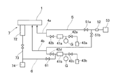
図3に示すように、第1ガス供給管4aには、バッファタンク41aと、このバッファタンク41aの上流側及び下流側の開閉弁42a,42bと、真空計Gとが夫々介設され、第1原料ガスのガス源43aに連通している。他方、第2ガス供給管4bもまた、バッファタンク41bと、このバッファタンク41bの上流側及び下流側の開閉弁42c,42dと、真空計Gとが夫々介設され、第2原料ガスのガス源43bに連通している。そして、各バッファタンク41a,41b内に予め充填されている第1原料ガスと第2原料ガスとが交互に供給されるようになっている。なお、ガス源43a、43bにおいては、気相状態の原料ガスを収納することができ、液相及び固相の原料を気化して原料ガスを得るようにしてもよい。
As shown in FIG. 3, the first
また、第1ガス供給管4aと第2ガス供給管4bとには、窒素ガスやアルゴンガス等の不活性ガスを導入する、開閉弁51a,51bとマスフローコントローラ52とが介設された不活性ガス源53からの不活性ガス導入管5が接続されており、成膜中、常時不活性ガスが真空チャンバ1内に導入され、例えば、第1原料ガスを基板Wに供給した後、第2原料ガスを基板Wに供給するのに先立ち、不活性ガスにより真空チャンバ1を一旦不活性ガス雰囲気に置換できるようにしている。なお、第2ガス供給管4bを、バッファタンク41bと下流側の開閉弁42dとの間で分岐し、この分岐されたバイパス管6を、開閉弁61を介して後述の排気チャンバに接続してもよい。
Further, the first
下隔壁11の周側壁12の内側部分でステージ2の左側には、真空チャンバ1の下壁及び下隔壁11を貫通させて排気手段7としての排気口71が開設されている。排気口71の前後方向の長さL3は、これに対向する基板Wの一辺の長さL2と同等以上の長さを有するように形成される。そして、この排気口71は、真空チャンバ1の下壁外側に設けた排気チャンバ72に連通している。排気チャンバ72には、他の排気管73を介して真空ポンプ74が接続されている。真空ポンプ74としては、ターボ分子ポンプやロータリーポンプなどの公知のものが利用され、また排気管73には、排気速度を調節する調節弁を備えていてもよい。また、排気チャンバ72としては筒状部材で構成されるものが利用され、鉛直方向にのびるように排気管73が吊設される。この場合、排気チャンバ72は、ガス流量等を考慮してその容積が設定される。
On the left side of the
真空チャンバ1内の上部には、下隔壁11に対向する上隔壁13が設けられている。上隔壁13は、真空チャンバ1の上壁を貫通して設けた複数本の駆動軸81に吊設され、その内部には図示省略のヒータが内蔵されている。真空チャンバ1外にのびる駆動軸81の部分にはベローズ82が外挿され、直動モータ等の駆動手段83に接続されている。この駆動手段83により、上隔壁13は、真空チャンバ1内の上側に退避して基板Wの搬送時に十分な搬送空間が確保できる搬送位置と、この上壁部13の周縁部が周側壁12の上面12aに密接して、噴射ノズル31,32および排気口71を含むステージ2の周囲を囲って真空チャンバ1の容積より小さい容積で真空チャンバ1から隔絶された成膜空間を画成する成膜位置との間で上下動される。なお、基板Wをステージ2に搬出、搬入するため、真空チャンバ1の側面にはゲートバルブGVが設けられると共に、ステージ2には、このステージから基板Wを持ち上げる図示省略のリフトピンが設けられ、図外のロボットハンドを備えた搬送ロボットで基板Wが搬送できるようになっている。
An
次に、本実施形態の真空処理装置による基板への成膜処理を説明する。図1に示す状態で、真空処理装置Mは、全ての開閉弁42a〜42dが閉弁され、上隔壁13が搬送位置にある状態で真空ポンプ74によりその内部が所定圧力まで真空排気されて待機状態となっている。次に、図示省略の搬送ロボットにより基板Wがステージ2の直上まで搬送され、リフトピンに受け渡された後、ステージ2上に載置される。この場合、静電チャック等により吸着してもよい。基板Wがステージ2上に載置されると、駆動手段83により上隔壁13を下動させ、成膜位置に移動する。このとき、バッファタンク41a,41bには、上流側の開閉弁42a,42cのみ開弁して第1原料ガスと第2原料ガスとが夫々充填され、真空計Gの測定値が所定値に達すると、両開閉弁42a,42cが閉弁される。
Next, the film forming process on the substrate by the vacuum processing apparatus of this embodiment will be described. In the state shown in FIG. 1, in the vacuum processing apparatus M, all the on-off
成膜を開始するとき、下流側の開閉弁42bと、不活性ガス用の開閉弁51a、51bとを開弁し、バッファタンク41a内の第1原料ガスと不活性ガスとを基板W表面に供給し、この第1原料ガスを処理表面に化学吸着させて第1原料ガスの原子の層を形成する。バッファタンク41a内の第1原料ガスが基板W表面に供給されると、下流側の開閉弁42bのみを閉弁し、基板W表面のガス雰囲気を不活性ガスにより置換する。次に、基板W表面のガス雰囲気を不活性ガスにより置換されると、下流側の開閉弁42dを開弁し、バッファタンク41b内の第2原料ガスと不活性ガスとを基板W表面に供給し、基板W表面に吸着されている第1反応ガスと反応させ、第2原料ガスの原子の層を形成する。このとき、バッファタンク41aには、上流側の開閉弁42aのみ開弁して第1原料ガスが充填され、真空計Gの測定値が所定値に達すると、開閉弁42aが閉弁される。この一連の操作を繰り返し、二種以上の原料ガスを交互に供給して化学反応により酸化アルミニウムが成膜される。
When starting the film formation, the downstream opening /
上記実施形態によれば、噴射ノズル31,32により、ステージ2の一側に配置されて基板Wの一側から他側に向けてかつこの基板W上面に沿って所定のガスを供給すると共に、真空チャンバ1の圧力より低い圧力となる排気チャンバ72に通じる排気口71をステージ2の他側に設けて基板Wを通過したガスが積極的に排気口71を介して排気チャンバ72に排気されるため、基板Wの成膜面全面に亘って原料ガスを効果的に吸着させることができる。この場合、排気チャンバ72が真空チャンバ1の下方に設けられ、しかも、噴射ノズル31,32を真空チャンバ1内に配置して、この噴射ノズル31,32に所定のガスを供給するガス供給管4a,4bを真空チャンバ1の下方から接続することができる構成であるため、配管や排気管等の部品を真空チャンバ1の壁面から側方に延出させて設ける必要がなく、装置の設置面積が大きくなることはなく、その上、クラスターツール用の成膜モジュールとする場合でも特段の制約は受けない。
According to the above embodiment, the
また、噴射ノズル31,32及び排気手段7を上記の如く構成することで、基板Wの成膜面全面に亘って一様にガスが流れるため、基板Wの成膜面全面に亘って原料ガスを吸着させることができ、しかも、成膜面で吸着されないガスが基板Wを通過すると直ちに排気することができる。
Further, since the
更に、上下動する上隔壁13及び下隔壁11を真空チャンバ1内に設けたことで、成膜時には容積の小さい成膜空間にすることができる一方で、基板Wの搬送時には十分な搬送空間を確保することができ、有利である。
Furthermore, by providing the
以上、本発明の実施形態について説明したが、本発明は上記のものに限定されるものではない。上記実施形態では、基板Wの成膜面全面に亘って一様に原料ガスを供給するため、基板Wの最大長と同等以上の噴射口31d,32dを設けたものを例に説明したが、これに限定されるものではなく、例えば、基板Wの長さ方向に複数本のガス管を列設してもよく、また、ノズル部31b,32bのステージ2側の端部に、長手方向に等間隔で透孔が列設された板状部材を設け、その長手方向に所定間隔を存して複数の噴射口が列設されるように構成してもよい。また、排気口71を複数の排気口から構成することもできる。
As mentioned above, although embodiment of this invention was described, this invention is not limited to said thing. In the above embodiment, in order to supply the source gas uniformly over the entire film formation surface of the substrate W, the example in which the
更に、上記実施形態では、2個の噴射ノズルを設けて2種類の原料ガスを導入するものを例に説明したが、これに限定されるものではなく、単一の噴射ノズルで複数種の原料ガスを導入することもできる。また、上隔壁13を板状部材としこれを上下動するものを例に説明したが、これに限定されるものではない。例えば、周壁部を上隔壁13の下面周縁部に形成することができ、この場合、真空チャンバ1の下壁に下隔壁11としての機能を持たせて省略することもできる。
Furthermore, in the above-described embodiment, an example in which two injection nozzles are provided and two types of raw material gases are introduced has been described as an example. Gas can also be introduced. Further, although the
M…真空成膜装置、1…真空チャンバ、2…ステージ、3…ガス供給手段、31,32…噴射ノズル、7…排気手段、71…排気口、73…排気チャンバ、75…真空ポンプ。 DESCRIPTION OF SYMBOLS M ... Vacuum film-forming apparatus, 1 ... Vacuum chamber, 2 ... Stage, 3 ... Gas supply means, 31, 32 ... Injection nozzle, 7 ... Exhaust means, 71 ... Exhaust port, 73 ... Exhaust chamber, 75 ... Vacuum pump.
Claims (4)
真空チャンバ内で基板を保持するステージと、この基板に対しガスを交互に供給するガス供給手段と、真空チャンバ内のガスを排気する排気手段と、を備え、
前記ステージで保持された前記基板の成膜面側を上とし、前記ガス供給手段は、ステージの一側に配置されて基板の一側から他側に向けてかつこの基板上面に沿って前記ガスのいずれかを噴射する少なくとも1個の噴射ノズルを有し、
前記排気手段は、前記ステージの他側で真空チャンバの下壁に開設される排気口と、この真空チャンバの下方に設けられて排気口に連通する排気チャンバと、排気チャンバに接続されてこの排気チャンバ内を真空引きする真空ポンプとを有することを特徴とする真空成膜装置。 In a vacuum film forming apparatus for forming a predetermined thin film by a chemical reaction by alternately supplying two or more kinds of gases to a substrate to be formed disposed in a vacuum chamber,
A stage for holding the substrate in the vacuum chamber, a gas supply means for alternately supplying gas to the substrate, and an exhaust means for exhausting the gas in the vacuum chamber,
The deposition surface side of the substrate held by the stage is up, and the gas supply unit is disposed on one side of the stage and moves from one side of the substrate to the other side and along the upper surface of the substrate. Having at least one injection nozzle for injecting any of
The exhaust means includes an exhaust port provided in a lower wall of the vacuum chamber on the other side of the stage, an exhaust chamber provided below the vacuum chamber and communicating with the exhaust port, and an exhaust chamber connected to the exhaust chamber. A vacuum film forming apparatus comprising: a vacuum pump that evacuates the chamber.
Priority Applications (4)
| Application Number | Priority Date | Filing Date | Title |
|---|---|---|---|
| JP2012012749A JP2013151720A (en) | 2012-01-25 | 2012-01-25 | Vacuum film forming apparatus |
| US13/735,623 US20130186340A1 (en) | 2012-01-25 | 2013-01-07 | Vacuum Film Forming Apparatus |
| CN2013100228441A CN103225073A (en) | 2012-01-25 | 2013-01-22 | Vacuum film forming apparatus |
| TW102102462A TWI564429B (en) | 2012-01-25 | 2013-01-23 | Vacuum film forming apparatus |
Applications Claiming Priority (1)
| Application Number | Priority Date | Filing Date | Title |
|---|---|---|---|
| JP2012012749A JP2013151720A (en) | 2012-01-25 | 2012-01-25 | Vacuum film forming apparatus |
Publications (2)
| Publication Number | Publication Date |
|---|---|
| JP2013151720A true JP2013151720A (en) | 2013-08-08 |
| JP2013151720A5 JP2013151720A5 (en) | 2014-12-04 |
Family
ID=48796182
Family Applications (1)
| Application Number | Title | Priority Date | Filing Date |
|---|---|---|---|
| JP2012012749A Pending JP2013151720A (en) | 2012-01-25 | 2012-01-25 | Vacuum film forming apparatus |
Country Status (4)
| Country | Link |
|---|---|
| US (1) | US20130186340A1 (en) |
| JP (1) | JP2013151720A (en) |
| CN (1) | CN103225073A (en) |
| TW (1) | TWI564429B (en) |
Cited By (3)
| Publication number | Priority date | Publication date | Assignee | Title |
|---|---|---|---|---|
| JP2015173226A (en) * | 2014-03-12 | 2015-10-01 | 株式会社アルバック | Vacuum deposition apparatus and deposition method using this apparatus |
| US20160329223A1 (en) * | 2013-12-25 | 2016-11-10 | Ushio Denki Kabushiki Kaisha | Light irradiation apparatus |
| JP2023036572A (en) * | 2021-09-02 | 2023-03-14 | ウォニク アイピーエス カンパニー リミテッド | Substrate processing apparatus |
Families Citing this family (237)
| Publication number | Priority date | Publication date | Assignee | Title |
|---|---|---|---|---|
| US9394608B2 (en) | 2009-04-06 | 2016-07-19 | Asm America, Inc. | Semiconductor processing reactor and components thereof |
| US8802201B2 (en) | 2009-08-14 | 2014-08-12 | Asm America, Inc. | Systems and methods for thin-film deposition of metal oxides using excited nitrogen-oxygen species |
| US20130023129A1 (en) | 2011-07-20 | 2013-01-24 | Asm America, Inc. | Pressure transmitter for a semiconductor processing environment |
| US9017481B1 (en) | 2011-10-28 | 2015-04-28 | Asm America, Inc. | Process feed management for semiconductor substrate processing |
| US10714315B2 (en) | 2012-10-12 | 2020-07-14 | Asm Ip Holdings B.V. | Semiconductor reaction chamber showerhead |
| US20160376700A1 (en) | 2013-02-01 | 2016-12-29 | Asm Ip Holding B.V. | System for treatment of deposition reactor |
| US11015245B2 (en) | 2014-03-19 | 2021-05-25 | Asm Ip Holding B.V. | Gas-phase reactor and system having exhaust plenum and components thereof |
| US10858737B2 (en) | 2014-07-28 | 2020-12-08 | Asm Ip Holding B.V. | Showerhead assembly and components thereof |
| US9890456B2 (en) | 2014-08-21 | 2018-02-13 | Asm Ip Holding B.V. | Method and system for in situ formation of gas-phase compounds |
| US10941490B2 (en) | 2014-10-07 | 2021-03-09 | Asm Ip Holding B.V. | Multiple temperature range susceptor, assembly, reactor and system including the susceptor, and methods of using the same |
| US10276355B2 (en) | 2015-03-12 | 2019-04-30 | Asm Ip Holding B.V. | Multi-zone reactor, system including the reactor, and method of using the same |
| US10458018B2 (en) | 2015-06-26 | 2019-10-29 | Asm Ip Holding B.V. | Structures including metal carbide material, devices including the structures, and methods of forming same |
| KR102397908B1 (en) * | 2015-08-19 | 2022-05-16 | 삼성전자주식회사 | Thin film deposition apparutus |
| US10211308B2 (en) | 2015-10-21 | 2019-02-19 | Asm Ip Holding B.V. | NbMC layers |
| US11139308B2 (en) | 2015-12-29 | 2021-10-05 | Asm Ip Holding B.V. | Atomic layer deposition of III-V compounds to form V-NAND devices |
| US10529554B2 (en) | 2016-02-19 | 2020-01-07 | Asm Ip Holding B.V. | Method for forming silicon nitride film selectively on sidewalls or flat surfaces of trenches |
| US10190213B2 (en) | 2016-04-21 | 2019-01-29 | Asm Ip Holding B.V. | Deposition of metal borides |
| US10865475B2 (en) | 2016-04-21 | 2020-12-15 | Asm Ip Holding B.V. | Deposition of metal borides and silicides |
| US10367080B2 (en) | 2016-05-02 | 2019-07-30 | Asm Ip Holding B.V. | Method of forming a germanium oxynitride film |
| US11453943B2 (en) | 2016-05-25 | 2022-09-27 | Asm Ip Holding B.V. | Method for forming carbon-containing silicon/metal oxide or nitride film by ALD using silicon precursor and hydrocarbon precursor |
| US10612137B2 (en) | 2016-07-08 | 2020-04-07 | Asm Ip Holdings B.V. | Organic reactants for atomic layer deposition |
| US9859151B1 (en) | 2016-07-08 | 2018-01-02 | Asm Ip Holding B.V. | Selective film deposition method to form air gaps |
| KR102532607B1 (en) | 2016-07-28 | 2023-05-15 | 에이에스엠 아이피 홀딩 비.브이. | Substrate processing apparatus and method of operating the same |
| US9887082B1 (en) | 2016-07-28 | 2018-02-06 | Asm Ip Holding B.V. | Method and apparatus for filling a gap |
| US9812320B1 (en) | 2016-07-28 | 2017-11-07 | Asm Ip Holding B.V. | Method and apparatus for filling a gap |
| US10643826B2 (en) | 2016-10-26 | 2020-05-05 | Asm Ip Holdings B.V. | Methods for thermally calibrating reaction chambers |
| US11532757B2 (en) | 2016-10-27 | 2022-12-20 | Asm Ip Holding B.V. | Deposition of charge trapping layers |
| US10714350B2 (en) | 2016-11-01 | 2020-07-14 | ASM IP Holdings, B.V. | Methods for forming a transition metal niobium nitride film on a substrate by atomic layer deposition and related semiconductor device structures |
| US10229833B2 (en) | 2016-11-01 | 2019-03-12 | Asm Ip Holding B.V. | Methods for forming a transition metal nitride film on a substrate by atomic layer deposition and related semiconductor device structures |
| KR102546317B1 (en) | 2016-11-15 | 2023-06-21 | 에이에스엠 아이피 홀딩 비.브이. | Gas supply unit and substrate processing apparatus including the same |
| KR20180068582A (en) | 2016-12-14 | 2018-06-22 | 에이에스엠 아이피 홀딩 비.브이. | Substrate processing apparatus |
| US11581186B2 (en) | 2016-12-15 | 2023-02-14 | Asm Ip Holding B.V. | Sequential infiltration synthesis apparatus |
| US11447861B2 (en) | 2016-12-15 | 2022-09-20 | Asm Ip Holding B.V. | Sequential infiltration synthesis apparatus and a method of forming a patterned structure |
| KR20180070971A (en) * | 2016-12-19 | 2018-06-27 | 에이에스엠 아이피 홀딩 비.브이. | Substrate processing apparatus |
| US10269558B2 (en) | 2016-12-22 | 2019-04-23 | Asm Ip Holding B.V. | Method of forming a structure on a substrate |
| US10867788B2 (en) | 2016-12-28 | 2020-12-15 | Asm Ip Holding B.V. | Method of forming a structure on a substrate |
| US11390950B2 (en) | 2017-01-10 | 2022-07-19 | Asm Ip Holding B.V. | Reactor system and method to reduce residue buildup during a film deposition process |
| US10468261B2 (en) | 2017-02-15 | 2019-11-05 | Asm Ip Holding B.V. | Methods for forming a metallic film on a substrate by cyclical deposition and related semiconductor device structures |
| US10529563B2 (en) | 2017-03-29 | 2020-01-07 | Asm Ip Holdings B.V. | Method for forming doped metal oxide films on a substrate by cyclical deposition and related semiconductor device structures |
| KR102457289B1 (en) | 2017-04-25 | 2022-10-21 | 에이에스엠 아이피 홀딩 비.브이. | Method for depositing a thin film and manufacturing a semiconductor device |
| US10892156B2 (en) | 2017-05-08 | 2021-01-12 | Asm Ip Holding B.V. | Methods for forming a silicon nitride film on a substrate and related semiconductor device structures |
| US10770286B2 (en) | 2017-05-08 | 2020-09-08 | Asm Ip Holdings B.V. | Methods for selectively forming a silicon nitride film on a substrate and related semiconductor device structures |
| US10886123B2 (en) | 2017-06-02 | 2021-01-05 | Asm Ip Holding B.V. | Methods for forming low temperature semiconductor layers and related semiconductor device structures |
| US11306395B2 (en) | 2017-06-28 | 2022-04-19 | Asm Ip Holding B.V. | Methods for depositing a transition metal nitride film on a substrate by atomic layer deposition and related deposition apparatus |
| KR20190009245A (en) | 2017-07-18 | 2019-01-28 | 에이에스엠 아이피 홀딩 비.브이. | Methods for forming a semiconductor device structure and related semiconductor device structures |
| US10541333B2 (en) | 2017-07-19 | 2020-01-21 | Asm Ip Holding B.V. | Method for depositing a group IV semiconductor and related semiconductor device structures |
| US11018002B2 (en) | 2017-07-19 | 2021-05-25 | Asm Ip Holding B.V. | Method for selectively depositing a Group IV semiconductor and related semiconductor device structures |
| US11374112B2 (en) | 2017-07-19 | 2022-06-28 | Asm Ip Holding B.V. | Method for depositing a group IV semiconductor and related semiconductor device structures |
| US10590535B2 (en) | 2017-07-26 | 2020-03-17 | Asm Ip Holdings B.V. | Chemical treatment, deposition and/or infiltration apparatus and method for using the same |
| US10770336B2 (en) | 2017-08-08 | 2020-09-08 | Asm Ip Holding B.V. | Substrate lift mechanism and reactor including same |
| US10692741B2 (en) | 2017-08-08 | 2020-06-23 | Asm Ip Holdings B.V. | Radiation shield |
| US11139191B2 (en) | 2017-08-09 | 2021-10-05 | Asm Ip Holding B.V. | Storage apparatus for storing cassettes for substrates and processing apparatus equipped therewith |
| US11769682B2 (en) | 2017-08-09 | 2023-09-26 | Asm Ip Holding B.V. | Storage apparatus for storing cassettes for substrates and processing apparatus equipped therewith |
| US11830730B2 (en) | 2017-08-29 | 2023-11-28 | Asm Ip Holding B.V. | Layer forming method and apparatus |
| KR102491945B1 (en) | 2017-08-30 | 2023-01-26 | 에이에스엠 아이피 홀딩 비.브이. | Substrate processing apparatus |
| US11056344B2 (en) | 2017-08-30 | 2021-07-06 | Asm Ip Holding B.V. | Layer forming method |
| US11295980B2 (en) | 2017-08-30 | 2022-04-05 | Asm Ip Holding B.V. | Methods for depositing a molybdenum metal film over a dielectric surface of a substrate by a cyclical deposition process and related semiconductor device structures |
| KR102630301B1 (en) | 2017-09-21 | 2024-01-29 | 에이에스엠 아이피 홀딩 비.브이. | Method of sequential infiltration synthesis treatment of infiltrateable material and structures and devices formed using same |
| US10844484B2 (en) | 2017-09-22 | 2020-11-24 | Asm Ip Holding B.V. | Apparatus for dispensing a vapor phase reactant to a reaction chamber and related methods |
| US10658205B2 (en) | 2017-09-28 | 2020-05-19 | Asm Ip Holdings B.V. | Chemical dispensing apparatus and methods for dispensing a chemical to a reaction chamber |
| US10403504B2 (en) | 2017-10-05 | 2019-09-03 | Asm Ip Holding B.V. | Method for selectively depositing a metallic film on a substrate |
| US10923344B2 (en) | 2017-10-30 | 2021-02-16 | Asm Ip Holding B.V. | Methods for forming a semiconductor structure and related semiconductor structures |
| US10910262B2 (en) | 2017-11-16 | 2021-02-02 | Asm Ip Holding B.V. | Method of selectively depositing a capping layer structure on a semiconductor device structure |
| US11022879B2 (en) | 2017-11-24 | 2021-06-01 | Asm Ip Holding B.V. | Method of forming an enhanced unexposed photoresist layer |
| US11639811B2 (en) | 2017-11-27 | 2023-05-02 | Asm Ip Holding B.V. | Apparatus including a clean mini environment |
| KR102597978B1 (en) | 2017-11-27 | 2023-11-06 | 에이에스엠 아이피 홀딩 비.브이. | Storage device for storing wafer cassettes for use with batch furnaces |
| US10872771B2 (en) | 2018-01-16 | 2020-12-22 | Asm Ip Holding B. V. | Method for depositing a material film on a substrate within a reaction chamber by a cyclical deposition process and related device structures |
| TW202325889A (en) | 2018-01-19 | 2023-07-01 | 荷蘭商Asm 智慧財產控股公司 | Deposition method |
| US11482412B2 (en) | 2018-01-19 | 2022-10-25 | Asm Ip Holding B.V. | Method for depositing a gap-fill layer by plasma-assisted deposition |
| US11018047B2 (en) | 2018-01-25 | 2021-05-25 | Asm Ip Holding B.V. | Hybrid lift pin |
| USD880437S1 (en) | 2018-02-01 | 2020-04-07 | Asm Ip Holding B.V. | Gas supply plate for semiconductor manufacturing apparatus |
| US11081345B2 (en) | 2018-02-06 | 2021-08-03 | Asm Ip Holding B.V. | Method of post-deposition treatment for silicon oxide film |
| US10896820B2 (en) | 2018-02-14 | 2021-01-19 | Asm Ip Holding B.V. | Method for depositing a ruthenium-containing film on a substrate by a cyclical deposition process |
| WO2019158960A1 (en) | 2018-02-14 | 2019-08-22 | Asm Ip Holding B.V. | A method for depositing a ruthenium-containing film on a substrate by a cyclical deposition process |
| KR102636427B1 (en) | 2018-02-20 | 2024-02-13 | 에이에스엠 아이피 홀딩 비.브이. | Substrate processing method and apparatus |
| US10975470B2 (en) | 2018-02-23 | 2021-04-13 | Asm Ip Holding B.V. | Apparatus for detecting or monitoring for a chemical precursor in a high temperature environment |
| US11473195B2 (en) | 2018-03-01 | 2022-10-18 | Asm Ip Holding B.V. | Semiconductor processing apparatus and a method for processing a substrate |
| US11629406B2 (en) | 2018-03-09 | 2023-04-18 | Asm Ip Holding B.V. | Semiconductor processing apparatus comprising one or more pyrometers for measuring a temperature of a substrate during transfer of the substrate |
| US11114283B2 (en) | 2018-03-16 | 2021-09-07 | Asm Ip Holding B.V. | Reactor, system including the reactor, and methods of manufacturing and using same |
| KR102646467B1 (en) | 2018-03-27 | 2024-03-11 | 에이에스엠 아이피 홀딩 비.브이. | Method of forming an electrode on a substrate and a semiconductor device structure including an electrode |
| US11230766B2 (en) | 2018-03-29 | 2022-01-25 | Asm Ip Holding B.V. | Substrate processing apparatus and method |
| US11088002B2 (en) | 2018-03-29 | 2021-08-10 | Asm Ip Holding B.V. | Substrate rack and a substrate processing system and method |
| KR102501472B1 (en) | 2018-03-30 | 2023-02-20 | 에이에스엠 아이피 홀딩 비.브이. | Substrate processing method |
| TWI811348B (en) | 2018-05-08 | 2023-08-11 | 荷蘭商Asm 智慧財產控股公司 | Methods for depositing an oxide film on a substrate by a cyclical deposition process and related device structures |
| TWI816783B (en) | 2018-05-11 | 2023-10-01 | 荷蘭商Asm 智慧財產控股公司 | Methods for forming a doped metal carbide film on a substrate and related semiconductor device structures |
| KR102596988B1 (en) | 2018-05-28 | 2023-10-31 | 에이에스엠 아이피 홀딩 비.브이. | Method of processing a substrate and a device manufactured by the same |
| US11270899B2 (en) | 2018-06-04 | 2022-03-08 | Asm Ip Holding B.V. | Wafer handling chamber with moisture reduction |
| US11718913B2 (en) | 2018-06-04 | 2023-08-08 | Asm Ip Holding B.V. | Gas distribution system and reactor system including same |
| US11286562B2 (en) | 2018-06-08 | 2022-03-29 | Asm Ip Holding B.V. | Gas-phase chemical reactor and method of using same |
| KR102568797B1 (en) | 2018-06-21 | 2023-08-21 | 에이에스엠 아이피 홀딩 비.브이. | Substrate processing system |
| US10797133B2 (en) | 2018-06-21 | 2020-10-06 | Asm Ip Holding B.V. | Method for depositing a phosphorus doped silicon arsenide film and related semiconductor device structures |
| CN112292477A (en) | 2018-06-27 | 2021-01-29 | Asm Ip私人控股有限公司 | Cyclic deposition methods for forming metal-containing materials and films and structures containing metal-containing materials |
| JP2021529254A (en) | 2018-06-27 | 2021-10-28 | エーエスエム・アイピー・ホールディング・ベー・フェー | Periodic deposition methods for forming metal-containing materials and films and structures containing metal-containing materials |
| US10612136B2 (en) | 2018-06-29 | 2020-04-07 | ASM IP Holding, B.V. | Temperature-controlled flange and reactor system including same |
| KR20200002519A (en) | 2018-06-29 | 2020-01-08 | 에이에스엠 아이피 홀딩 비.브이. | Method for depositing a thin film and manufacturing a semiconductor device |
| US10755922B2 (en) | 2018-07-03 | 2020-08-25 | Asm Ip Holding B.V. | Method for depositing silicon-free carbon-containing film as gap-fill layer by pulse plasma-assisted deposition |
| US10388513B1 (en) | 2018-07-03 | 2019-08-20 | Asm Ip Holding B.V. | Method for depositing silicon-free carbon-containing film as gap-fill layer by pulse plasma-assisted deposition |
| US10767789B2 (en) | 2018-07-16 | 2020-09-08 | Asm Ip Holding B.V. | Diaphragm valves, valve components, and methods for forming valve components |
| US11053591B2 (en) | 2018-08-06 | 2021-07-06 | Asm Ip Holding B.V. | Multi-port gas injection system and reactor system including same |
| US10883175B2 (en) | 2018-08-09 | 2021-01-05 | Asm Ip Holding B.V. | Vertical furnace for processing substrates and a liner for use therein |
| US10829852B2 (en) | 2018-08-16 | 2020-11-10 | Asm Ip Holding B.V. | Gas distribution device for a wafer processing apparatus |
| US11430674B2 (en) | 2018-08-22 | 2022-08-30 | Asm Ip Holding B.V. | Sensor array, apparatus for dispensing a vapor phase reactant to a reaction chamber and related methods |
| US11024523B2 (en) | 2018-09-11 | 2021-06-01 | Asm Ip Holding B.V. | Substrate processing apparatus and method |
| KR20200030162A (en) | 2018-09-11 | 2020-03-20 | 에이에스엠 아이피 홀딩 비.브이. | Method for deposition of a thin film |
| US11049751B2 (en) | 2018-09-14 | 2021-06-29 | Asm Ip Holding B.V. | Cassette supply system to store and handle cassettes and processing apparatus equipped therewith |
| CN110970344A (en) | 2018-10-01 | 2020-04-07 | Asm Ip控股有限公司 | Substrate holding apparatus, system including the same, and method of using the same |
| US11232963B2 (en) | 2018-10-03 | 2022-01-25 | Asm Ip Holding B.V. | Substrate processing apparatus and method |
| KR102592699B1 (en) | 2018-10-08 | 2023-10-23 | 에이에스엠 아이피 홀딩 비.브이. | Substrate support unit and apparatuses for depositing thin film and processing the substrate including the same |
| KR102546322B1 (en) | 2018-10-19 | 2023-06-21 | 에이에스엠 아이피 홀딩 비.브이. | Substrate processing apparatus and substrate processing method |
| KR102605121B1 (en) | 2018-10-19 | 2023-11-23 | 에이에스엠 아이피 홀딩 비.브이. | Substrate processing apparatus and substrate processing method |
| USD948463S1 (en) | 2018-10-24 | 2022-04-12 | Asm Ip Holding B.V. | Susceptor for semiconductor substrate supporting apparatus |
| US11087997B2 (en) | 2018-10-31 | 2021-08-10 | Asm Ip Holding B.V. | Substrate processing apparatus for processing substrates |
| KR20200051105A (en) | 2018-11-02 | 2020-05-13 | 에이에스엠 아이피 홀딩 비.브이. | Substrate support unit and substrate processing apparatus including the same |
| US11572620B2 (en) | 2018-11-06 | 2023-02-07 | Asm Ip Holding B.V. | Methods for selectively depositing an amorphous silicon film on a substrate |
| US11031242B2 (en) | 2018-11-07 | 2021-06-08 | Asm Ip Holding B.V. | Methods for depositing a boron doped silicon germanium film |
| US10818758B2 (en) | 2018-11-16 | 2020-10-27 | Asm Ip Holding B.V. | Methods for forming a metal silicate film on a substrate in a reaction chamber and related semiconductor device structures |
| US10847366B2 (en) | 2018-11-16 | 2020-11-24 | Asm Ip Holding B.V. | Methods for depositing a transition metal chalcogenide film on a substrate by a cyclical deposition process |
| US11217444B2 (en) | 2018-11-30 | 2022-01-04 | Asm Ip Holding B.V. | Method for forming an ultraviolet radiation responsive metal oxide-containing film |
| KR102636428B1 (en) | 2018-12-04 | 2024-02-13 | 에이에스엠 아이피 홀딩 비.브이. | A method for cleaning a substrate processing apparatus |
| US11158513B2 (en) | 2018-12-13 | 2021-10-26 | Asm Ip Holding B.V. | Methods for forming a rhenium-containing film on a substrate by a cyclical deposition process and related semiconductor device structures |
| JP2020096183A (en) | 2018-12-14 | 2020-06-18 | エーエスエム・アイピー・ホールディング・ベー・フェー | Method of forming device structure using selective deposition of gallium nitride, and system for the same |
| TWI819180B (en) | 2019-01-17 | 2023-10-21 | 荷蘭商Asm 智慧財產控股公司 | Methods of forming a transition metal containing film on a substrate by a cyclical deposition process |
| KR20200091543A (en) | 2019-01-22 | 2020-07-31 | 에이에스엠 아이피 홀딩 비.브이. | Semiconductor processing device |
| CN111524788B (en) | 2019-02-01 | 2023-11-24 | Asm Ip私人控股有限公司 | Method for topologically selective film formation of silicon oxide |
| JP2020136677A (en) | 2019-02-20 | 2020-08-31 | エーエスエム・アイピー・ホールディング・ベー・フェー | Periodic accumulation method for filing concave part formed inside front surface of base material, and device |
| KR102626263B1 (en) | 2019-02-20 | 2024-01-16 | 에이에스엠 아이피 홀딩 비.브이. | Cyclical deposition method including treatment step and apparatus for same |
| US11482533B2 (en) | 2019-02-20 | 2022-10-25 | Asm Ip Holding B.V. | Apparatus and methods for plug fill deposition in 3-D NAND applications |
| KR102638425B1 (en) | 2019-02-20 | 2024-02-21 | 에이에스엠 아이피 홀딩 비.브이. | Method and apparatus for filling a recess formed within a substrate surface |
| JP2020133004A (en) | 2019-02-22 | 2020-08-31 | エーエスエム・アイピー・ホールディング・ベー・フェー | Base material processing apparatus and method for processing base material |
| KR20200108243A (en) | 2019-03-08 | 2020-09-17 | 에이에스엠 아이피 홀딩 비.브이. | Structure Including SiOC Layer and Method of Forming Same |
| KR20200108242A (en) | 2019-03-08 | 2020-09-17 | 에이에스엠 아이피 홀딩 비.브이. | Method for Selective Deposition of Silicon Nitride Layer and Structure Including Selectively-Deposited Silicon Nitride Layer |
| US11742198B2 (en) | 2019-03-08 | 2023-08-29 | Asm Ip Holding B.V. | Structure including SiOCN layer and method of forming same |
| JP2020167398A (en) | 2019-03-28 | 2020-10-08 | エーエスエム・アイピー・ホールディング・ベー・フェー | Door opener and substrate processing apparatus provided therewith |
| KR20200116855A (en) | 2019-04-01 | 2020-10-13 | 에이에스엠 아이피 홀딩 비.브이. | Method of manufacturing semiconductor device |
| US11447864B2 (en) | 2019-04-19 | 2022-09-20 | Asm Ip Holding B.V. | Layer forming method and apparatus |
| KR20200125453A (en) | 2019-04-24 | 2020-11-04 | 에이에스엠 아이피 홀딩 비.브이. | Gas-phase reactor system and method of using same |
| KR20200130118A (en) | 2019-05-07 | 2020-11-18 | 에이에스엠 아이피 홀딩 비.브이. | Method for Reforming Amorphous Carbon Polymer Film |
| KR20200130121A (en) | 2019-05-07 | 2020-11-18 | 에이에스엠 아이피 홀딩 비.브이. | Chemical source vessel with dip tube |
| KR20200130652A (en) | 2019-05-10 | 2020-11-19 | 에이에스엠 아이피 홀딩 비.브이. | Method of depositing material onto a surface and structure formed according to the method |
| JP2020188255A (en) | 2019-05-16 | 2020-11-19 | エーエスエム アイピー ホールディング ビー.ブイ. | Wafer boat handling device, vertical batch furnace, and method |
| USD947913S1 (en) | 2019-05-17 | 2022-04-05 | Asm Ip Holding B.V. | Susceptor shaft |
| USD975665S1 (en) | 2019-05-17 | 2023-01-17 | Asm Ip Holding B.V. | Susceptor shaft |
| USD935572S1 (en) | 2019-05-24 | 2021-11-09 | Asm Ip Holding B.V. | Gas channel plate |
| USD922229S1 (en) | 2019-06-05 | 2021-06-15 | Asm Ip Holding B.V. | Device for controlling a temperature of a gas supply unit |
| KR20200141002A (en) | 2019-06-06 | 2020-12-17 | 에이에스엠 아이피 홀딩 비.브이. | Method of using a gas-phase reactor system including analyzing exhausted gas |
| KR20200143254A (en) | 2019-06-11 | 2020-12-23 | 에이에스엠 아이피 홀딩 비.브이. | Method of forming an electronic structure using an reforming gas, system for performing the method, and structure formed using the method |
| USD944946S1 (en) | 2019-06-14 | 2022-03-01 | Asm Ip Holding B.V. | Shower plate |
| USD931978S1 (en) | 2019-06-27 | 2021-09-28 | Asm Ip Holding B.V. | Showerhead vacuum transport |
| KR20210005515A (en) | 2019-07-03 | 2021-01-14 | 에이에스엠 아이피 홀딩 비.브이. | Temperature control assembly for substrate processing apparatus and method of using same |
| JP2021015791A (en) | 2019-07-09 | 2021-02-12 | エーエスエム アイピー ホールディング ビー.ブイ. | Plasma device and substrate processing method using coaxial waveguide |
| CN112216646A (en) | 2019-07-10 | 2021-01-12 | Asm Ip私人控股有限公司 | Substrate supporting assembly and substrate processing device comprising same |
| KR20210010307A (en) | 2019-07-16 | 2021-01-27 | 에이에스엠 아이피 홀딩 비.브이. | Substrate processing apparatus |
| KR20210010816A (en) | 2019-07-17 | 2021-01-28 | 에이에스엠 아이피 홀딩 비.브이. | Radical assist ignition plasma system and method |
| KR20210010820A (en) | 2019-07-17 | 2021-01-28 | 에이에스엠 아이피 홀딩 비.브이. | Methods of forming silicon germanium structures |
| US11643724B2 (en) | 2019-07-18 | 2023-05-09 | Asm Ip Holding B.V. | Method of forming structures using a neutral beam |
| CN112242296A (en) | 2019-07-19 | 2021-01-19 | Asm Ip私人控股有限公司 | Method of forming topologically controlled amorphous carbon polymer films |
| TW202113936A (en) | 2019-07-29 | 2021-04-01 | 荷蘭商Asm Ip私人控股有限公司 | Methods for selective deposition utilizing n-type dopants and/or alternative dopants to achieve high dopant incorporation |
| CN112309899A (en) | 2019-07-30 | 2021-02-02 | Asm Ip私人控股有限公司 | Substrate processing apparatus |
| CN112309900A (en) | 2019-07-30 | 2021-02-02 | Asm Ip私人控股有限公司 | Substrate processing apparatus |
| US11587814B2 (en) | 2019-07-31 | 2023-02-21 | Asm Ip Holding B.V. | Vertical batch furnace assembly |
| US11227782B2 (en) | 2019-07-31 | 2022-01-18 | Asm Ip Holding B.V. | Vertical batch furnace assembly |
| US11587815B2 (en) | 2019-07-31 | 2023-02-21 | Asm Ip Holding B.V. | Vertical batch furnace assembly |
| CN112323048B (en) | 2019-08-05 | 2024-02-09 | Asm Ip私人控股有限公司 | Liquid level sensor for chemical source container |
| USD965044S1 (en) | 2019-08-19 | 2022-09-27 | Asm Ip Holding B.V. | Susceptor shaft |
| USD965524S1 (en) | 2019-08-19 | 2022-10-04 | Asm Ip Holding B.V. | Susceptor support |
| JP2021031769A (en) | 2019-08-21 | 2021-03-01 | エーエスエム アイピー ホールディング ビー.ブイ. | Production apparatus of mixed gas of film deposition raw material and film deposition apparatus |
| USD979506S1 (en) | 2019-08-22 | 2023-02-28 | Asm Ip Holding B.V. | Insulator |
| USD930782S1 (en) | 2019-08-22 | 2021-09-14 | Asm Ip Holding B.V. | Gas distributor |
| USD949319S1 (en) | 2019-08-22 | 2022-04-19 | Asm Ip Holding B.V. | Exhaust duct |
| KR20210024423A (en) | 2019-08-22 | 2021-03-05 | 에이에스엠 아이피 홀딩 비.브이. | Method for forming a structure with a hole |
| USD940837S1 (en) | 2019-08-22 | 2022-01-11 | Asm Ip Holding B.V. | Electrode |
| US11286558B2 (en) | 2019-08-23 | 2022-03-29 | Asm Ip Holding B.V. | Methods for depositing a molybdenum nitride film on a surface of a substrate by a cyclical deposition process and related semiconductor device structures including a molybdenum nitride film |
| KR20210024420A (en) | 2019-08-23 | 2021-03-05 | 에이에스엠 아이피 홀딩 비.브이. | Method for depositing silicon oxide film having improved quality by peald using bis(diethylamino)silane |
| KR20210029090A (en) | 2019-09-04 | 2021-03-15 | 에이에스엠 아이피 홀딩 비.브이. | Methods for selective deposition using a sacrificial capping layer |
| KR20210029663A (en) | 2019-09-05 | 2021-03-16 | 에이에스엠 아이피 홀딩 비.브이. | Substrate processing apparatus |
| US11562901B2 (en) | 2019-09-25 | 2023-01-24 | Asm Ip Holding B.V. | Substrate processing method |
| CN112593212B (en) | 2019-10-02 | 2023-12-22 | Asm Ip私人控股有限公司 | Method for forming topologically selective silicon oxide film by cyclic plasma enhanced deposition process |
| TW202129060A (en) | 2019-10-08 | 2021-08-01 | 荷蘭商Asm Ip控股公司 | Substrate processing device, and substrate processing method |
| TW202115273A (en) | 2019-10-10 | 2021-04-16 | 荷蘭商Asm Ip私人控股有限公司 | Method of forming a photoresist underlayer and structure including same |
| KR20210045930A (en) | 2019-10-16 | 2021-04-27 | 에이에스엠 아이피 홀딩 비.브이. | Method of Topology-Selective Film Formation of Silicon Oxide |
| US11637014B2 (en) | 2019-10-17 | 2023-04-25 | Asm Ip Holding B.V. | Methods for selective deposition of doped semiconductor material |
| KR20210047808A (en) | 2019-10-21 | 2021-04-30 | 에이에스엠 아이피 홀딩 비.브이. | Apparatus and methods for selectively etching films |
| US11646205B2 (en) | 2019-10-29 | 2023-05-09 | Asm Ip Holding B.V. | Methods of selectively forming n-type doped material on a surface, systems for selectively forming n-type doped material, and structures formed using same |
| US11779949B2 (en) * | 2019-10-30 | 2023-10-10 | Taiwan Semiconductor Manufacturing Co., Ltd. | Semiconductor process chamber contamination prevention system |
| KR20210054983A (en) | 2019-11-05 | 2021-05-14 | 에이에스엠 아이피 홀딩 비.브이. | Structures with doped semiconductor layers and methods and systems for forming same |
| US11501968B2 (en) | 2019-11-15 | 2022-11-15 | Asm Ip Holding B.V. | Method for providing a semiconductor device with silicon filled gaps |
| KR20210062561A (en) | 2019-11-20 | 2021-05-31 | 에이에스엠 아이피 홀딩 비.브이. | Method of depositing carbon-containing material on a surface of a substrate, structure formed using the method, and system for forming the structure |
| US11450529B2 (en) | 2019-11-26 | 2022-09-20 | Asm Ip Holding B.V. | Methods for selectively forming a target film on a substrate comprising a first dielectric surface and a second metallic surface |
| CN112951697A (en) | 2019-11-26 | 2021-06-11 | Asm Ip私人控股有限公司 | Substrate processing apparatus |
| CN112885692A (en) | 2019-11-29 | 2021-06-01 | Asm Ip私人控股有限公司 | Substrate processing apparatus |
| CN112885693A (en) | 2019-11-29 | 2021-06-01 | Asm Ip私人控股有限公司 | Substrate processing apparatus |
| JP2021090042A (en) | 2019-12-02 | 2021-06-10 | エーエスエム アイピー ホールディング ビー.ブイ. | Substrate processing apparatus and substrate processing method |
| KR20210070898A (en) | 2019-12-04 | 2021-06-15 | 에이에스엠 아이피 홀딩 비.브이. | Substrate processing apparatus |
| JP2021097227A (en) | 2019-12-17 | 2021-06-24 | エーエスエム・アイピー・ホールディング・ベー・フェー | Method of forming vanadium nitride layer and structure including vanadium nitride layer |
| US11527403B2 (en) | 2019-12-19 | 2022-12-13 | Asm Ip Holding B.V. | Methods for filling a gap feature on a substrate surface and related semiconductor structures |
| JP2021109175A (en) | 2020-01-06 | 2021-08-02 | エーエスエム・アイピー・ホールディング・ベー・フェー | Gas supply assembly, components thereof, and reactor system including the same |
| KR20210095050A (en) | 2020-01-20 | 2021-07-30 | 에이에스엠 아이피 홀딩 비.브이. | Method of forming thin film and method of modifying surface of thin film |
| TW202130846A (en) | 2020-02-03 | 2021-08-16 | 荷蘭商Asm Ip私人控股有限公司 | Method of forming structures including a vanadium or indium layer |
| TW202146882A (en) | 2020-02-04 | 2021-12-16 | 荷蘭商Asm Ip私人控股有限公司 | Method of verifying an article, apparatus for verifying an article, and system for verifying a reaction chamber |
| US11776846B2 (en) | 2020-02-07 | 2023-10-03 | Asm Ip Holding B.V. | Methods for depositing gap filling fluids and related systems and devices |
| US11781243B2 (en) | 2020-02-17 | 2023-10-10 | Asm Ip Holding B.V. | Method for depositing low temperature phosphorous-doped silicon |
| TW202203344A (en) | 2020-02-28 | 2022-01-16 | 荷蘭商Asm Ip控股公司 | System dedicated for parts cleaning |
| KR20210116240A (en) | 2020-03-11 | 2021-09-27 | 에이에스엠 아이피 홀딩 비.브이. | Substrate handling device with adjustable joints |
| US11876356B2 (en) | 2020-03-11 | 2024-01-16 | Asm Ip Holding B.V. | Lockout tagout assembly and system and method of using same |
| CN113394086A (en) | 2020-03-12 | 2021-09-14 | Asm Ip私人控股有限公司 | Method for producing a layer structure having a target topological profile |
| KR20210124042A (en) | 2020-04-02 | 2021-10-14 | 에이에스엠 아이피 홀딩 비.브이. | Thin film forming method |
| TW202146689A (en) | 2020-04-03 | 2021-12-16 | 荷蘭商Asm Ip控股公司 | Method for forming barrier layer and method for manufacturing semiconductor device |
| TW202145344A (en) | 2020-04-08 | 2021-12-01 | 荷蘭商Asm Ip私人控股有限公司 | Apparatus and methods for selectively etching silcon oxide films |
| US11821078B2 (en) | 2020-04-15 | 2023-11-21 | Asm Ip Holding B.V. | Method for forming precoat film and method for forming silicon-containing film |
| KR20210132600A (en) | 2020-04-24 | 2021-11-04 | 에이에스엠 아이피 홀딩 비.브이. | Methods and systems for depositing a layer comprising vanadium, nitrogen, and a further element |
| CN113555279A (en) | 2020-04-24 | 2021-10-26 | Asm Ip私人控股有限公司 | Method of forming vanadium nitride-containing layers and structures including the same |
| TW202146831A (en) | 2020-04-24 | 2021-12-16 | 荷蘭商Asm Ip私人控股有限公司 | Vertical batch furnace assembly, and method for cooling vertical batch furnace |
| KR20210134226A (en) | 2020-04-29 | 2021-11-09 | 에이에스엠 아이피 홀딩 비.브이. | Solid source precursor vessel |
| KR20210134869A (en) | 2020-05-01 | 2021-11-11 | 에이에스엠 아이피 홀딩 비.브이. | Fast FOUP swapping with a FOUP handler |
| KR20210141379A (en) | 2020-05-13 | 2021-11-23 | 에이에스엠 아이피 홀딩 비.브이. | Laser alignment fixture for a reactor system |
| TW202147383A (en) | 2020-05-19 | 2021-12-16 | 荷蘭商Asm Ip私人控股有限公司 | Substrate processing apparatus |
| KR20210145078A (en) | 2020-05-21 | 2021-12-01 | 에이에스엠 아이피 홀딩 비.브이. | Structures including multiple carbon layers and methods of forming and using same |
| KR20210145080A (en) | 2020-05-22 | 2021-12-01 | 에이에스엠 아이피 홀딩 비.브이. | Apparatus for depositing thin films using hydrogen peroxide |
| TW202201602A (en) | 2020-05-29 | 2022-01-01 | 荷蘭商Asm Ip私人控股有限公司 | Substrate processing device |
| TW202218133A (en) | 2020-06-24 | 2022-05-01 | 荷蘭商Asm Ip私人控股有限公司 | Method for forming a layer provided with silicon |
| TW202217953A (en) | 2020-06-30 | 2022-05-01 | 荷蘭商Asm Ip私人控股有限公司 | Substrate processing method |
| KR20220010438A (en) | 2020-07-17 | 2022-01-25 | 에이에스엠 아이피 홀딩 비.브이. | Structures and methods for use in photolithography |
| TW202204662A (en) | 2020-07-20 | 2022-02-01 | 荷蘭商Asm Ip私人控股有限公司 | Method and system for depositing molybdenum layers |
| TW202212623A (en) | 2020-08-26 | 2022-04-01 | 荷蘭商Asm Ip私人控股有限公司 | Method of forming metal silicon oxide layer and metal silicon oxynitride layer, semiconductor structure, and system |
| USD990534S1 (en) | 2020-09-11 | 2023-06-27 | Asm Ip Holding B.V. | Weighted lift pin |
| USD1012873S1 (en) | 2020-09-24 | 2024-01-30 | Asm Ip Holding B.V. | Electrode for semiconductor processing apparatus |
| TW202229613A (en) | 2020-10-14 | 2022-08-01 | 荷蘭商Asm Ip私人控股有限公司 | Method of depositing material on stepped structure |
| TW202217037A (en) | 2020-10-22 | 2022-05-01 | 荷蘭商Asm Ip私人控股有限公司 | Method of depositing vanadium metal, structure, device and a deposition assembly |
| TW202223136A (en) | 2020-10-28 | 2022-06-16 | 荷蘭商Asm Ip私人控股有限公司 | Method for forming layer on substrate, and semiconductor processing system |
| KR20220076343A (en) | 2020-11-30 | 2022-06-08 | 에이에스엠 아이피 홀딩 비.브이. | an injector configured for arrangement within a reaction chamber of a substrate processing apparatus |
| US11946137B2 (en) | 2020-12-16 | 2024-04-02 | Asm Ip Holding B.V. | Runout and wobble measurement fixtures |
| TW202231903A (en) | 2020-12-22 | 2022-08-16 | 荷蘭商Asm Ip私人控股有限公司 | Transition metal deposition method, transition metal layer, and deposition assembly for depositing transition metal on substrate |
| USD980813S1 (en) | 2021-05-11 | 2023-03-14 | Asm Ip Holding B.V. | Gas flow control plate for substrate processing apparatus |
| USD980814S1 (en) | 2021-05-11 | 2023-03-14 | Asm Ip Holding B.V. | Gas distributor for substrate processing apparatus |
| USD1023959S1 (en) | 2021-05-11 | 2024-04-23 | Asm Ip Holding B.V. | Electrode for substrate processing apparatus |
| USD981973S1 (en) | 2021-05-11 | 2023-03-28 | Asm Ip Holding B.V. | Reactor wall for substrate processing apparatus |
| USD990441S1 (en) | 2021-09-07 | 2023-06-27 | Asm Ip Holding B.V. | Gas flow control plate |
Citations (2)
| Publication number | Priority date | Publication date | Assignee | Title |
|---|---|---|---|---|
| JPH104064A (en) * | 1996-06-17 | 1998-01-06 | Toshiba Mach Co Ltd | Single wafer processing low pressure cvd apparatus |
| JP2002151489A (en) * | 2000-08-11 | 2002-05-24 | Tokyo Electron Ltd | Substrate processing apparatus and processing method |
Family Cites Families (10)
| Publication number | Priority date | Publication date | Assignee | Title |
|---|---|---|---|---|
| EP1308992A4 (en) * | 2000-08-11 | 2006-01-18 | Tokyo Electron Ltd | Device and method for processing substrate |
| JP2003133299A (en) * | 2001-10-24 | 2003-05-09 | Oki Electric Ind Co Ltd | Apparatus and method for manufacturing semiconductor |
| JP2006176826A (en) * | 2004-12-22 | 2006-07-06 | Canon Anelva Corp | Thin film treatment device |
| JP2007273515A (en) * | 2006-03-30 | 2007-10-18 | Mitsui Eng & Shipbuild Co Ltd | Thin film forming apparatus |
| JP4961948B2 (en) * | 2006-10-27 | 2012-06-27 | 東京エレクトロン株式会社 | Plasma processing apparatus, plasma processing method, and storage medium |
| JP4973150B2 (en) * | 2006-11-27 | 2012-07-11 | 東京エレクトロン株式会社 | Gas introduction mechanism and processing object processing object |
| WO2009108221A2 (en) * | 2008-02-27 | 2009-09-03 | S.O.I.Tec Silicon On Insulator Technologies | Thermalization of gaseous precursors in cvd reactors |
| JP5573772B2 (en) * | 2010-06-22 | 2014-08-20 | 東京エレクトロン株式会社 | Film forming method and film forming apparatus |
| JP5687547B2 (en) * | 2010-06-28 | 2015-03-18 | 株式会社日立国際電気 | Semiconductor device manufacturing method, substrate processing method, and substrate processing apparatus |
| KR101313262B1 (en) * | 2010-07-12 | 2013-09-30 | 삼성전자주식회사 | Chemical Vapor Deposition Apparatus and Method of Forming Semiconductor Thin Film Using The Same |
-
2012
- 2012-01-25 JP JP2012012749A patent/JP2013151720A/en active Pending
-
2013
- 2013-01-07 US US13/735,623 patent/US20130186340A1/en not_active Abandoned
- 2013-01-22 CN CN2013100228441A patent/CN103225073A/en active Pending
- 2013-01-23 TW TW102102462A patent/TWI564429B/en active
Patent Citations (2)
| Publication number | Priority date | Publication date | Assignee | Title |
|---|---|---|---|---|
| JPH104064A (en) * | 1996-06-17 | 1998-01-06 | Toshiba Mach Co Ltd | Single wafer processing low pressure cvd apparatus |
| JP2002151489A (en) * | 2000-08-11 | 2002-05-24 | Tokyo Electron Ltd | Substrate processing apparatus and processing method |
Cited By (4)
| Publication number | Priority date | Publication date | Assignee | Title |
|---|---|---|---|---|
| US20160329223A1 (en) * | 2013-12-25 | 2016-11-10 | Ushio Denki Kabushiki Kaisha | Light irradiation apparatus |
| JP2015173226A (en) * | 2014-03-12 | 2015-10-01 | 株式会社アルバック | Vacuum deposition apparatus and deposition method using this apparatus |
| JP2023036572A (en) * | 2021-09-02 | 2023-03-14 | ウォニク アイピーエス カンパニー リミテッド | Substrate processing apparatus |
| JP7441905B2 (en) | 2021-09-02 | 2024-03-01 | ウォニク アイピーエス カンパニー リミテッド | Substrate processing equipment |
Also Published As
| Publication number | Publication date |
|---|---|
| US20130186340A1 (en) | 2013-07-25 |
| TWI564429B (en) | 2017-01-01 |
| TW201350618A (en) | 2013-12-16 |
| CN103225073A (en) | 2013-07-31 |
Similar Documents
| Publication | Publication Date | Title |
|---|---|---|
| JP2013151720A (en) | Vacuum film forming apparatus | |
| CN112962084B (en) | Substrate processing apparatus | |
| CN109559975B (en) | Substrate processing apparatus, reaction tube, method for manufacturing semiconductor device, and program | |
| KR101138810B1 (en) | Substrate processing apparatus | |
| JP2013151720A5 (en) | ||
| KR101535683B1 (en) | Film formation apparatus, substrate processing apparatus, film formation method and storage medium | |
| JP4523661B1 (en) | Atomic layer deposition apparatus and thin film forming method | |
| KR102197576B1 (en) | Apparatus for spatial atomic layer deposition with recirculation and methods of use | |
| JP4634495B2 (en) | Substrate processing apparatus and semiconductor device manufacturing method | |
| US20190330738A1 (en) | Substrate Processing Apparatus, Reaction Tube and Method of Manufacturing Semiconductor Device | |
| JP6151829B2 (en) | Substrate processing equipment | |
| TWI601232B (en) | Support structure and processing apparatus | |
| JP2015517210A (en) | Equipment and cluster equipment for selective epitaxial growth | |
| WO2018050953A1 (en) | Apparatus and methods for atomic layer deposition | |
| TWI741093B (en) | Temporal atomic layer deposition processing chamber | |
| KR101685096B1 (en) | Apparatus for processing substrate and method for processing substrate using the same | |
| JP6462139B2 (en) | Gas supply unit, substrate processing apparatus, and method for manufacturing semiconductor device | |
| EP2465972B1 (en) | Method and system for thin film deposition | |
| JP6363408B2 (en) | Film forming apparatus and film forming method | |
| JP2013136839A (en) | Vacuum processing system | |
| JP2011029441A (en) | Device and method for treating substrate | |
| JP2009267345A (en) | Substrate processing apparatus | |
| KR102349330B1 (en) | Thin film encapsulation processing system and process kit | |
| KR101555238B1 (en) | Semiconductor Apparatus of Furnace Type | |
| KR101431087B1 (en) | apparatus for Selctive Epitaxial Growth and Cluster Apparatus |
Legal Events
| Date | Code | Title | Description |
|---|---|---|---|
| A521 | Written amendment |
Free format text: JAPANESE INTERMEDIATE CODE: A523 Effective date: 20141017 |
|
| A621 | Written request for application examination |
Free format text: JAPANESE INTERMEDIATE CODE: A621 Effective date: 20141017 |
|
| A977 | Report on retrieval |
Free format text: JAPANESE INTERMEDIATE CODE: A971007 Effective date: 20150416 |
|
| A131 | Notification of reasons for refusal |
Free format text: JAPANESE INTERMEDIATE CODE: A131 Effective date: 20150512 |
|
| A02 | Decision of refusal |
Free format text: JAPANESE INTERMEDIATE CODE: A02 Effective date: 20151027 |