JP2013143407A - Method of manufacturing laminated soi wafer - Google Patents
Method of manufacturing laminated soi wafer Download PDFInfo
- Publication number
- JP2013143407A JP2013143407A JP2012001611A JP2012001611A JP2013143407A JP 2013143407 A JP2013143407 A JP 2013143407A JP 2012001611 A JP2012001611 A JP 2012001611A JP 2012001611 A JP2012001611 A JP 2012001611A JP 2013143407 A JP2013143407 A JP 2013143407A
- Authority
- JP
- Japan
- Prior art keywords
- wafer
- rta
- temperature
- soi wafer
- ion
- Prior art date
- Legal status (The legal status is an assumption and is not a legal conclusion. Google has not performed a legal analysis and makes no representation as to the accuracy of the status listed.)
- Pending
Links
Images


Classifications
-
- H—ELECTRICITY
- H01—ELECTRIC ELEMENTS
- H01L—SEMICONDUCTOR DEVICES NOT COVERED BY CLASS H10
- H01L21/00—Processes or apparatus adapted for the manufacture or treatment of semiconductor or solid state devices or of parts thereof
- H01L21/70—Manufacture or treatment of devices consisting of a plurality of solid state components formed in or on a common substrate or of parts thereof; Manufacture of integrated circuit devices or of parts thereof
- H01L21/71—Manufacture of specific parts of devices defined in group H01L21/70
- H01L21/76—Making of isolation regions between components
- H01L21/762—Dielectric regions, e.g. EPIC dielectric isolation, LOCOS; Trench refilling techniques, SOI technology, use of channel stoppers
- H01L21/7624—Dielectric regions, e.g. EPIC dielectric isolation, LOCOS; Trench refilling techniques, SOI technology, use of channel stoppers using semiconductor on insulator [SOI] technology
- H01L21/76251—Dielectric regions, e.g. EPIC dielectric isolation, LOCOS; Trench refilling techniques, SOI technology, use of channel stoppers using semiconductor on insulator [SOI] technology using bonding techniques
- H01L21/76254—Dielectric regions, e.g. EPIC dielectric isolation, LOCOS; Trench refilling techniques, SOI technology, use of channel stoppers using semiconductor on insulator [SOI] technology using bonding techniques with separation/delamination along an ion implanted layer, e.g. Smart-cut, Unibond
-
- H—ELECTRICITY
- H01—ELECTRIC ELEMENTS
- H01L—SEMICONDUCTOR DEVICES NOT COVERED BY CLASS H10
- H01L21/00—Processes or apparatus adapted for the manufacture or treatment of semiconductor or solid state devices or of parts thereof
- H01L21/02—Manufacture or treatment of semiconductor devices or of parts thereof
- H01L21/04—Manufacture or treatment of semiconductor devices or of parts thereof the devices having at least one potential-jump barrier or surface barrier, e.g. PN junction, depletion layer or carrier concentration layer
- H01L21/18—Manufacture or treatment of semiconductor devices or of parts thereof the devices having at least one potential-jump barrier or surface barrier, e.g. PN junction, depletion layer or carrier concentration layer the devices having semiconductor bodies comprising elements of Group IV of the Periodic System or AIIIBV compounds with or without impurities, e.g. doping materials
- H01L21/30—Treatment of semiconductor bodies using processes or apparatus not provided for in groups H01L21/20 - H01L21/26
- H01L21/302—Treatment of semiconductor bodies using processes or apparatus not provided for in groups H01L21/20 - H01L21/26 to change their surface-physical characteristics or shape, e.g. etching, polishing, cutting
- H01L21/306—Chemical or electrical treatment, e.g. electrolytic etching
- H01L21/30604—Chemical etching
-
- H—ELECTRICITY
- H01—ELECTRIC ELEMENTS
- H01L—SEMICONDUCTOR DEVICES NOT COVERED BY CLASS H10
- H01L21/00—Processes or apparatus adapted for the manufacture or treatment of semiconductor or solid state devices or of parts thereof
- H01L21/02—Manufacture or treatment of semiconductor devices or of parts thereof
- H01L21/04—Manufacture or treatment of semiconductor devices or of parts thereof the devices having at least one potential-jump barrier or surface barrier, e.g. PN junction, depletion layer or carrier concentration layer
- H01L21/18—Manufacture or treatment of semiconductor devices or of parts thereof the devices having at least one potential-jump barrier or surface barrier, e.g. PN junction, depletion layer or carrier concentration layer the devices having semiconductor bodies comprising elements of Group IV of the Periodic System or AIIIBV compounds with or without impurities, e.g. doping materials
- H01L21/30—Treatment of semiconductor bodies using processes or apparatus not provided for in groups H01L21/20 - H01L21/26
- H01L21/324—Thermal treatment for modifying the properties of semiconductor bodies, e.g. annealing, sintering
-
- H—ELECTRICITY
- H01—ELECTRIC ELEMENTS
- H01L—SEMICONDUCTOR DEVICES NOT COVERED BY CLASS H10
- H01L21/00—Processes or apparatus adapted for the manufacture or treatment of semiconductor or solid state devices or of parts thereof
- H01L21/02—Manufacture or treatment of semiconductor devices or of parts thereof
- H01L21/02104—Forming layers
- H01L21/02107—Forming insulating materials on a substrate
- H01L21/02225—Forming insulating materials on a substrate characterised by the process for the formation of the insulating layer
- H01L21/02227—Forming insulating materials on a substrate characterised by the process for the formation of the insulating layer formation by a process other than a deposition process
- H01L21/0223—Forming insulating materials on a substrate characterised by the process for the formation of the insulating layer formation by a process other than a deposition process formation by oxidation, e.g. oxidation of the substrate
- H01L21/02233—Forming insulating materials on a substrate characterised by the process for the formation of the insulating layer formation by a process other than a deposition process formation by oxidation, e.g. oxidation of the substrate of the semiconductor substrate or a semiconductor layer
- H01L21/02236—Forming insulating materials on a substrate characterised by the process for the formation of the insulating layer formation by a process other than a deposition process formation by oxidation, e.g. oxidation of the substrate of the semiconductor substrate or a semiconductor layer group IV semiconductor
- H01L21/02238—Forming insulating materials on a substrate characterised by the process for the formation of the insulating layer formation by a process other than a deposition process formation by oxidation, e.g. oxidation of the substrate of the semiconductor substrate or a semiconductor layer group IV semiconductor silicon in uncombined form, i.e. pure silicon
-
- H—ELECTRICITY
- H01—ELECTRIC ELEMENTS
- H01L—SEMICONDUCTOR DEVICES NOT COVERED BY CLASS H10
- H01L21/00—Processes or apparatus adapted for the manufacture or treatment of semiconductor or solid state devices or of parts thereof
- H01L21/02—Manufacture or treatment of semiconductor devices or of parts thereof
- H01L21/02104—Forming layers
- H01L21/02107—Forming insulating materials on a substrate
- H01L21/02225—Forming insulating materials on a substrate characterised by the process for the formation of the insulating layer
- H01L21/02227—Forming insulating materials on a substrate characterised by the process for the formation of the insulating layer formation by a process other than a deposition process
- H01L21/02255—Forming insulating materials on a substrate characterised by the process for the formation of the insulating layer formation by a process other than a deposition process formation by thermal treatment
Abstract
Description
本発明は、イオン注入剥離法を用いた貼り合わせSOIウェーハの製造方法に関し、特には、水素イオン等を注入したシリコン単結晶ウェーハを支持基板となるベースウェーハと貼り合わせた後に剥離して貼り合わせSOIウェーハを製造する方法に関する。 The present invention relates to a method for manufacturing a bonded SOI wafer using an ion implantation delamination method, and in particular, a silicon single crystal wafer implanted with hydrogen ions or the like is bonded to a base wafer serving as a support substrate, and then peeled and bonded. The present invention relates to a method for manufacturing an SOI wafer.
最近、貼り合わせSOIウェーハの製造方法として、イオン注入したボンドウェーハを貼り合わせた後に剥離して貼り合わせSOIウェーハを製造する方法(イオン注入剥離法:スマートカット法(登録商標)とも呼ばれる技術)が新たに注目され始めている。
このイオン注入剥離法は、二枚のウェーハの内、少なくとも一方に酸化膜を形成すると共に、一方のウェーハ(ボンドウェーハ)の上面から水素イオンや希ガスイオン等のガスイオンを注入し、該ウェーハ内部にイオン注入層(微小気泡層)を形成させた後、該イオンを注入した方の面を酸化膜(絶縁膜)を介して他方のウェーハ(ベースウェーハ)と密着させ、その後、熱処理(剥離熱処理)又は機械的な外力を加えてイオン注入層を劈開面として一方のウェーハ(ボンドウェーハ)を薄膜状に剥離し、さらに熱処理(結合熱処理)を加えて強固に結合してベースウェーハ上に薄膜(SOI層)を有する貼り合わせSOIウェーハを作製する技術(特許文献1参照)である。この方法では、薄膜、特にはSOI層の膜厚の均一性が高い貼り合わせSOIウェーハが容易に得られている。
Recently, as a method for manufacturing a bonded SOI wafer, there is a method of manufacturing a bonded SOI wafer by bonding and bonding an ion-implanted bond wafer (ion implantation separation method: a technique also called Smart Cut Method (registered trademark)). It has begun to attract new attention.
In this ion implantation separation method, an oxide film is formed on at least one of two wafers, and gas ions such as hydrogen ions and rare gas ions are implanted from the upper surface of one wafer (bond wafer). After an ion-implanted layer (microbubble layer) is formed inside, the surface into which the ions are implanted is brought into close contact with the other wafer (base wafer) through an oxide film (insulating film), and then heat treatment (peeling) Heat treatment) or mechanical external force is applied to peel off one wafer (bond wafer) into a thin film with the ion-implanted layer as a cleavage plane, and further heat treatment (bond heat treatment) to form a thin film on the base wafer. This is a technique for manufacturing a bonded SOI wafer having (SOI layer) (see Patent Document 1). In this method, a bonded SOI wafer having a high uniformity in the thickness of a thin film, particularly an SOI layer, can be easily obtained.
しかし、イオン注入剥離法により貼り合わせSOIウェーハを作製する場合においては、剥離後の貼り合わせSOIウェーハ表面にイオン注入によるダメージ層が存在し、また表面粗さが通常の製品レベルのシリコンウェーハの鏡面に比べて大きなものとなる。したがって、イオン注入剥離法では、このようなダメージ層、表面粗さを除去することが必要になる。 However, when a bonded SOI wafer is manufactured by an ion implantation peeling method, a damage layer due to ion implantation exists on the surface of the bonded SOI wafer after peeling, and the mirror surface of a silicon wafer having a normal product level surface roughness. Bigger than that. Therefore, in the ion implantation separation method, it is necessary to remove such a damaged layer and surface roughness.
従来、このダメージ層等を除去するために、結合熱処理後の最終工程において、タッチポリッシュと呼ばれる研磨代の極めて少ない鏡面研磨(取り代:100nm程度)が行われていた。
ところが、SOI層に機械加工的要素を含む研磨をしてしまうと、研磨の取り代が均一でないために、水素イオンなどの注入、剥離によってある程度達成されたSOI層の膜厚均一性が悪化してしまうという問題が生じる。
Conventionally, in order to remove the damaged layer and the like, mirror polishing (removal allowance: about 100 nm) called “polishing polish” has been performed in the final step after the bonding heat treatment.
However, if polishing including a machining element is performed on the SOI layer, since the polishing allowance is not uniform, the film thickness uniformity of the SOI layer achieved to some extent by implantation and peeling of hydrogen ions and the like deteriorates. Problem arises.
このような問題点を解決する方法として、前記タッチポリッシュの代わりに高温熱処理を行って表面粗さを改善する平坦化処理が行われるようになってきている。
例えば、特許文献2では、剥離熱処理後(または結合熱処理後)に、SOI層の表面を研磨することなく水素を含む還元性雰囲気下の熱処理(急速加熱・急速冷却熱処理(RTA:Rapid Thermal Annealing))を加えることを提案している。さらに、特許文献3では、剥離熱処理後(又は結合熱処理後)に、酸化性雰囲気下の熱処理によりSOI層に酸化膜を形成した後に該酸化膜を除去し(いわゆる犠牲酸化処理)、次に還元性雰囲気の熱処理(急速加熱・急速冷却熱処理(RTA処理))を加えることを提案している。
As a method for solving such a problem, a flattening process for improving the surface roughness by performing a high-temperature heat treatment instead of the touch polish has been performed.
For example, in Patent Document 2, a heat treatment in a reducing atmosphere containing hydrogen without polishing the surface of the SOI layer (or rapid thermal annealing (RTA)) after peeling heat treatment (or after bonding heat treatment). ). Further, in Patent Document 3, after the peeling heat treatment (or after the bonding heat treatment), after forming an oxide film on the SOI layer by heat treatment in an oxidizing atmosphere, the oxide film is removed (so-called sacrificial oxidation treatment), and then reduced. It is proposed to add a heat treatment (rapid heating / rapid cooling heat treatment (RTA treatment)) in a neutral atmosphere.
また、特許文献4では、剥離後のSOIウェーハに、不活性ガス、水素ガス、あるいはこれらの混合ガス雰囲気下での平坦化熱処理の後に犠牲酸化処理を行うことにより、剥離面の平坦化とOSF発生の回避を同時に達成している。
このように、タッチポリッシュの代わりに高温熱処理を行って表面粗さを改善する平坦化処理が行われるようになったことによって、現在では、直径300mmでSOI層の膜厚レンジ(面内の最大膜厚値から最小膜厚値を引いた値)が3nm以内の膜厚均一性を有するSOIウェーハが、イオン注入剥離法によって量産レベルで得られている。
In Patent Document 4, the SOI wafer after peeling is subjected to sacrificial oxidation treatment after planarization heat treatment in an inert gas, hydrogen gas, or mixed gas atmosphere thereof, thereby planarizing the peeled surface and OSF. At the same time avoidance of the occurrence.
As described above, a flattening process for improving the surface roughness by performing a high-temperature heat treatment instead of the touch polish is performed, and at present, the film thickness range of the SOI layer with a diameter of 300 mm (maximum in the plane). An SOI wafer having a film thickness uniformity of 3 nm or less (a value obtained by subtracting the minimum film thickness value from the film thickness value) is obtained at the mass production level by the ion implantation delamination method.
また、特許文献5には、剥離面の表面粗さを低減するため、少なくとも2つの異なる原子のイオン種の共注入を行い、その仕上げステップとして、「RTA+StabOx(安定化酸化)」を1回又は複数回行うことが記載されている([0046]段落参照)。[0078]段落に、このStabOx(安定化酸化(犠牲酸化))は、900℃酸化+1100℃Arアニール(2時間)であると記載されている。
特許文献6の[0087]段落でも同様に、イオン種の共注入による剥離面の表面粗さ改善として、RTA+StabOx+RTA+薄膜化を行うことが記載されている。
Further, in Patent Document 5, in order to reduce the surface roughness of the peeling surface, co-injection of ion species of at least two different atoms is performed, and “RTA + StabOx (stabilized oxidation)” is performed once or as a finishing step. Multiple times are described (see paragraph [0046]). [0078] In the paragraph, this StabOx (stabilized oxidation (sacrificial oxidation)) is described as 900 ° C. oxidation + 1100 ° C. Ar annealing (2 hours).
Similarly, in paragraph [0087] of Patent Document 6, it is described that RTA + StabOx + RTA + thinning is performed to improve the surface roughness of the peeled surface by co-implantation of ion species.
さらに、特許文献7の[0035]〜[0037]段落には、SOI層の欠陥(致命ホール)を低減するため、仕上げステップとしてRTAと犠牲酸化(SOx)が記載されているが、SOxの温度としては1100℃が開示されているのみである([0039]段落に記載されているRTA−SOx−RTA−SOxの参照文献(仏国特許)とは、特許文献5に対応)。 Further, in paragraphs [0035] to [0037] of Patent Document 7, RTA and sacrificial oxidation (SOx) are described as finishing steps in order to reduce defects (fatal holes) in the SOI layer. Only 1100 ° C. is disclosed (the RTA-SOx-RTA-SOx reference document (French patent) described in paragraph [0039] corresponds to Patent Document 5).
さらに、特許文献8には、SOI層の凹状欠陥を低減するため、剥離→オゾン洗浄→水素RTA(1100〜1250℃)→犠牲酸化→Arアニールのプロセスが記載されている(実施例では、RTA(1150℃/30sec)+Arアニール(1200℃/1hr))。 Further, Patent Document 8 describes a process of delamination → ozone cleaning → hydrogen RTA (1100 to 1250 ° C.) → sacrificial oxidation → Ar annealing in order to reduce concave defects in the SOI layer (in the embodiment, RTA). (1150 ° C./30 sec) + Ar annealing (1200 ° C./1 hr)).
特許文献5〜8に記載されているように、剥離面の表面粗さを改善したり、SOI層の欠陥を低減することなどを目的として、RTAと犠牲酸化を組み合わせた処理を行う方法がいくつか提案されている。
しかしながら、特許文献5、6における犠牲酸化は、900℃酸化+1100℃Arアニール(2時間)と記載されている通り、抵抗加熱式の熱処理炉(バッチ炉)を用いて酸化後に連続的に高温長時間のアニール(ポストアニール)を含む工程であるため、スリップ転位の発生頻度が高まるという問題があった。
As described in Patent Documents 5 to 8, there are several methods for performing treatment combining RTA and sacrificial oxidation for the purpose of improving the surface roughness of the peeled surface or reducing defects in the SOI layer. Or has been proposed.
However, as described in Patent Documents 5 and 6, sacrificial oxidation is performed at a high temperature continuously after oxidation using a resistance heating type heat treatment furnace (batch furnace) as described in 900 ° C. oxidation + 1100 ° C. Ar annealing (2 hours). Since this process includes annealing for a period of time (post-annealing), there is a problem that the frequency of occurrence of slip dislocation increases.
また、特許文献7では、StabOxの温度として1100℃が開示されているが、RTA処理を行った後であっても、このような高温で犠牲酸化を行うとSOI層の表面にOSF(酸化誘起積層欠陥)が発生してしまうという問題があった。さらに、特許文献8の方法は、SOI層の凹状欠陥を低減するのには有効であるが、犠牲酸化後のArアニールが高温長時間であるため、特許文献5、6と同様に、スリップ転位の発生頻度が高まるという問題があった。 In Patent Document 7, 1100 ° C. is disclosed as the temperature of StabOx. However, even after the RTA treatment, if sacrificial oxidation is performed at such a high temperature, OSF (oxidation induction) is formed on the surface of the SOI layer. There was a problem that stacking faults) occurred. Further, the method of Patent Document 8 is effective in reducing the concave defects in the SOI layer, but since Ar annealing after sacrificial oxidation is performed at a high temperature for a long time, slip dislocations are performed as in Patent Documents 5 and 6. There was a problem that the frequency of occurrence increased.
本発明は、上記問題点に鑑みてなされたものであって、イオン注入剥離法による貼り合わせSOIウェーハの製造において、剥離後のSOI層の表面粗さを改善しつつ、スリップ転位や欠陥の発生を抑制することができ、所望膜厚と優れた膜厚分布のSOI層を有する貼り合わせSOIウェーハを製造できる方法を提供することを目的とする。 The present invention has been made in view of the above problems, and in the production of a bonded SOI wafer by an ion implantation separation method, the occurrence of slip dislocations and defects while improving the surface roughness of the SOI layer after separation. An object of the present invention is to provide a method capable of manufacturing a bonded SOI wafer having an SOI layer having a desired film thickness and an excellent film thickness distribution.
上記目的を達成するために、本発明は、シリコン単結晶からなるボンドウェーハの表面から水素イオン、希ガスイオンの少なくとも一種類のガスイオンをイオン注入して該ボンドウェーハ内部にイオン注入層を形成し、前記ボンドウェーハのイオン注入された側の表面とベースウェーハの表面とを絶縁膜を介して貼り合わせた後、前記ボンドウェーハの一部を前記イオン注入層で剥離して、前記ベースウェーハ上にSOI層を有する貼り合わせSOIウェーハを製造する方法であって、前記剥離後の貼り合わせSOIウェーハに対して、第1のRTA処理を行った後、第1の犠牲酸化処理を行い、その後、第2のRTA処理を行った後、第2の犠牲酸化処理を行う工程を有し、前記第1及び第2のRTA処理を、水素ガス含有雰囲気下、1100℃以上の温度で行い、前記第1及び第2の犠牲酸化処理において、900℃以上1000℃以下の温度でバッチ式熱処理炉による熱酸化のみを行うことによって前記SOI層表面に熱酸化膜を形成した後、該熱酸化膜を除去する処理を行うことを特徴とする貼り合わせSOIウェーハの製造方法を提供する。 In order to achieve the above object, the present invention forms an ion-implanted layer inside a bond wafer by ion-implanting at least one kind of hydrogen ion or rare gas ion from the surface of a bond wafer made of a silicon single crystal. And bonding the ion-implanted surface of the bond wafer and the surface of the base wafer through an insulating film, and then peeling off a part of the bond wafer with the ion-implanted layer. A bonded SOI wafer having an SOI layer on the bonded SOI wafer, after the first RTA process is performed on the bonded SOI wafer after peeling, and then a first sacrificial oxidation process is performed. A step of performing a second sacrificial oxidation treatment after the second RTA treatment, and performing the first and second RTA treatments in a hydrogen gas-containing atmosphere; A thermal oxide film is formed on the surface of the SOI layer by performing only thermal oxidation in a batch heat treatment furnace at a temperature of 900 ° C. or higher and 1000 ° C. or lower in the first and second sacrificial oxidation processes. Provided is a method for manufacturing a bonded SOI wafer, wherein after the formation, the thermal oxide film is removed.
このように、剥離後の貼り合わせSOIウェーハに対して上記処理を行うことで、犠牲酸化処理時に高温長時間の非酸化性雰囲気のアニールを行わずに熱酸化のみを行うので、SOI層の平坦化と欠陥の抑制を達成でき、さらにイオン注入剥離により得られた膜厚均一性を維持することができる。また、高温長時間のアニールを行う必要が無いため、スリップ転位の発生を抑制し、かつプロセスの短縮化を図ることができる。従って、所望膜厚を有し、高品質なSOI層を有する貼り合わせSOIウェーハを製造することができる。 In this way, by performing the above-described processing on the bonded SOI wafer after peeling, only thermal oxidation is performed without performing annealing in a high-temperature and long-time non-oxidizing atmosphere during the sacrificial oxidation processing. And suppression of defects can be achieved, and the film thickness uniformity obtained by ion implantation separation can be maintained. In addition, since there is no need to perform annealing at a high temperature for a long time, the occurrence of slip dislocation can be suppressed and the process can be shortened. Therefore, a bonded SOI wafer having a desired film thickness and having a high-quality SOI layer can be manufactured.
このとき、前記第1及び第2の犠牲酸化処理における熱酸化の温度を、950℃以上とすることが好ましい。
このような温度で熱酸化することで、比較的厚い酸化膜をより短時間で形成することができ、生産性を向上させることができる。また、950℃以上でも、先にRTA処理を行って平坦化、イオン注入ダメージ層の回復が行われているためOSF等の欠陥は発生しない。
At this time, it is preferable that the temperature of thermal oxidation in the first and second sacrificial oxidation treatments be 950 ° C. or higher.
By performing thermal oxidation at such a temperature, a relatively thick oxide film can be formed in a shorter time, and productivity can be improved. Even at 950 ° C. or higher, defects such as OSF do not occur because the RTA treatment is performed first to planarize and recover the ion implantation damage layer.
このとき、前記ボンドウェーハと前記ベースウェーハの少なくとも一方の表面にプラズマ処理を施した後に前記絶縁膜を介して貼り合わせた後、前記ボンドウェーハの一部を前記イオン注入層で機械的な外力を用いて剥離することが好ましい。
このように貼り合わせ、機械的剥離を行うことで、剥離面の面粗さを低減でき、より効率的にSOI層を平坦化することができる。
At this time, after subjecting at least one surface of the bond wafer and the base wafer to plasma treatment and pasting them together via the insulating film, a mechanical external force is applied to a part of the bond wafer by the ion implantation layer. It is preferable to use and peel.
By performing bonding and mechanical peeling in this manner, the surface roughness of the peeled surface can be reduced, and the SOI layer can be planarized more efficiently.
このとき、前記第1及び第2のRTA処理を、1230℃以下の温度で行うことが好ましい。
このような温度で第1及び第2のRTA処理することで、スリップ転位の発生を確実に抑制することができる。
At this time, it is preferable that the first and second RTA processes are performed at a temperature of 1230 ° C. or lower.
By performing the first and second RTA processes at such a temperature, occurrence of slip dislocation can be reliably suppressed.
以上のように、本発明によれば、スリップ転位や欠陥の発生を抑制しながら、平坦で、膜厚均一性が高いSOI層を有する高品質な貼り合わせSOIウェーハを製造することができる。 As described above, according to the present invention, it is possible to manufacture a high-quality bonded SOI wafer having an SOI layer that is flat and has high film thickness uniformity while suppressing occurrence of slip dislocation and defects.
以下、本発明について、実施態様の一例として、図を参照しながら詳細に説明するが、本発明はこれに限定されるものではない。
図1は本発明の貼り合わせSOIウェーハの製造方法のフロー図である。
Hereinafter, the present invention will be described in detail as an example of an embodiment with reference to the drawings, but the present invention is not limited thereto.
FIG. 1 is a flowchart of a method for manufacturing a bonded SOI wafer according to the present invention.
まず、図1の工程(a)では、ボンドウェーハ10と支持基板となるベースウェーハ11として例えば鏡面研磨されたシリコン単結晶ウェーハを用意する。
First, in the step (a) of FIG. 1, for example, a mirror-polished silicon single crystal wafer is prepared as a
次に、図1の工程(b)では、例えば熱酸化やCVD酸化等によりボンドウェーハ10に酸化膜12を形成する。この酸化膜12は、ベースウェーハ11のみに形成してもよいし、両ウェーハに形成してもよい。
次に、図1の工程(c)では、水素イオン、希ガスイオンのうち少なくとも一種類のガスイオンを注入して、ボンドウェーハ10の内部にイオン注入層13を形成する。
Next, in step (b) of FIG. 1, an
Next, in step (c) of FIG. 1, at least one kind of gas ion is implanted among hydrogen ions and rare gas ions to form an
次に、図1の工程(d)では、ボンドウェーハ10のイオン注入された側の表面とベースウェーハ11の表面とを酸化膜12を介して密着させて貼り合わせる。
なお、貼り合わせる前に、ウェーハの表面に付着しているパーティクルおよび有機物を除去するため、両ウェーハに貼り合わせ前洗浄を行ってもよい。
Next, in the step (d) of FIG. 1, the surface of the
Before bonding, in order to remove particles and organic substances adhering to the surface of the wafer, both wafers may be cleaned before bonding.
次に、図1の工程(e)では、イオン注入層13を境界としてボンドウェーハ10を剥離させ、ベースウェーハ11上に埋め込み酸化膜14とSOI層16を形成し、貼り合わせSOIウェーハ15を得る。
Next, in the step (e) of FIG. 1, the
剥離方法としては、例えば熱処理を行わずに、あるいは、剥離しない程度の低温の熱処理を加えた後に機械的な外力を用いて剥離させる方法が好ましい。この場合には、貼り合わせ工程(d)の前にボンドウェーハ10とベースウェーハ11の少なくとも一方の表面にプラズマ処理を施して、貼り合わせ界面の結合強度を高めることが好ましい。
このように機械的な外力で剥離させることで、剥離面の面粗さを低減できるため、本発明のRTA処理で、十分に平坦化できるだけでなく、RTA処理の条件を緩和することも可能となる。
また、機械的な外力による剥離方法以外にも、例えば、不活性ガス雰囲気下、500℃以上の温度で熱処理を行い、結晶の再配列と気泡の凝集とによって剥離させることもできる。
As the peeling method, for example, a method of performing peeling using a mechanical external force without performing heat treatment or after applying a low-temperature heat treatment not to peel is preferable. In this case, it is preferable that at least one surface of the
Since the surface roughness of the peeled surface can be reduced by peeling with a mechanical external force in this way, the RTA treatment of the present invention can not only sufficiently planarize but also relax the conditions of the RTA treatment. Become.
In addition to the peeling method using mechanical external force, for example, heat treatment can be performed at a temperature of 500 ° C. or higher in an inert gas atmosphere, and peeling can be performed by crystal rearrangement and bubble aggregation.
次に、図1の工程(f)では、剥離後の貼り合わせSOIウェーハ15に対して、第1のRTA処理を行った後、第1の犠牲酸化処理を行い、その後、第2のRTA処理を行った後、第2の犠牲酸化処理を行う。
このとき、第1及び第2のRTA処理を、水素ガス含有雰囲気下、1100℃以上の温度で行う。また、第1及び第2の犠牲酸化処理において、900℃以上1000℃以下の温度でバッチ式熱処理炉による熱酸化のみを行うことによってSOI層16の表面に熱酸化膜を形成した後、該熱酸化膜を除去する処理を行う。
Next, in the step (f) of FIG. 1, the first RTA process is performed on the bonded
At this time, the first and second RTA processes are performed at a temperature of 1100 ° C. or higher in an atmosphere containing hydrogen gas. Further, in the first and second sacrificial oxidation treatments, a thermal oxide film is formed on the surface of the
従来の犠牲酸化処理は、900℃酸化+1100℃アニール(ポストアニール)を連続的に行うことによってSOI層の欠陥発生を抑制していた。しかし、本発明では、水素ガス含有雰囲気下、1100℃以上の温度でRTA処理を行うことで、犠牲酸化処理の熱酸化後のポストアニール(例えば1000℃を超える温度の非酸化性雰囲気の熱処理)を行わずに(すなわち、熱酸化のみで)SOI層を十分に平坦化及びダメージ層の回復が達成でき、長時間のポストアニールが不要なので、スリップ転位の発生率を低下させることができると同時にプロセスの短縮化を図ることができる。RTA処理により剥離面のダメージ層の回復及び平坦化を行ってから犠牲酸化処理を行うことができるため、熱酸化時の欠陥の発生を抑制できる。さらに、犠牲酸化処理により平坦化及び所望の膜厚まで薄膜化処理を行うことで、膜厚均一性を維持しながら所望膜厚を有する平坦なSOI層にすることができる。このような犠牲酸化処理の熱酸化は、予めRTA処理によりダメージ層の回復が行われているため900℃以上の温度で効率的に熱酸化膜を形成でき、また、1000℃以下の温度で実施することでSOI層の欠陥の発生を確実に抑制できる。このようなRTA処理、犠牲酸化処理を2回行うことで、十分にSOI層の平坦化及びダメージ除去が可能であり、また確実に所望膜厚にすることができる。 Conventional sacrificial oxidation treatment suppresses generation of defects in the SOI layer by continuously performing 900 ° C. oxidation + 1100 ° C. annealing (post-annealing). However, in the present invention, post-annealing after thermal oxidation of sacrificial oxidation treatment (for example, heat treatment in a non-oxidizing atmosphere at a temperature exceeding 1000 ° C.) is performed by performing RTA treatment at a temperature of 1100 ° C. or higher in an atmosphere containing hydrogen gas. (Ie, only by thermal oxidation), the SOI layer can be sufficiently flattened and the damaged layer can be recovered, and the post-annealing for a long time is not required. The process can be shortened. Since the sacrificial oxidation treatment can be performed after the damaged layer on the peeled surface is recovered and flattened by the RTA treatment, the occurrence of defects during thermal oxidation can be suppressed. Further, by performing the planarization and the thinning process to a desired film thickness by the sacrificial oxidation process, a flat SOI layer having a desired film thickness can be obtained while maintaining the film thickness uniformity. Thermal oxidation of such sacrificial oxidation treatment can be efficiently formed at a temperature of 900 ° C. or higher because the damaged layer is recovered by RTA treatment in advance, and is also performed at a temperature of 1000 ° C. or lower. By doing so, generation of defects in the SOI layer can be reliably suppressed. By performing the RTA process and the sacrificial oxidation process twice, the SOI layer can be sufficiently flattened and the damage can be removed, and the desired film thickness can be reliably obtained.
また、本発明の第1及び第2の犠牲酸化処理の熱酸化の温度を、950℃以上とすることが好ましい。
従来は、剥離直後の貼り合わせSOIウェーハに対して950℃以上の温度で熱酸化を行うと、SOI層表面に欠陥(OSF)が発生してしまうという問題があったが、本発明の場合、犠牲酸化の前に高温の水素RTA処理を行って表面の平坦化とイオン注入のダメージ層の回復が行われているため、熱酸化の温度を950℃以上(1000℃以下)にしてもOSFは発生しないことを本発明者らは見出した。従って、950℃以上で熱酸化を行うことで、比較的厚い酸化膜を形成する場合であっても酸化時間の短縮を図ることができ、生産効率を向上させることができる。
Moreover, it is preferable that the temperature of thermal oxidation in the first and second sacrificial oxidation treatments of the present invention is 950 ° C. or higher.
Conventionally, when thermal oxidation is performed on a bonded SOI wafer immediately after peeling at a temperature of 950 ° C. or higher, there is a problem that a defect (OSF) occurs on the surface of the SOI layer. Since high-temperature hydrogen RTA treatment is performed before sacrificial oxidation to flatten the surface and recover the damaged layer by ion implantation, the OSF can be achieved even if the thermal oxidation temperature is 950 ° C. or higher (1000 ° C. or lower). The inventors have found that this does not occur. Therefore, by performing thermal oxidation at 950 ° C. or higher, the oxidation time can be shortened even when a relatively thick oxide film is formed, and the production efficiency can be improved.
また、本発明の第1及び第2のRTA処理は短時間であるため、高温長時間のバッチ式熱処理炉の熱処理に比べてスリップ転位の発生頻度は低く、RTA処理温度を高くすると剥離面の平坦化効果が高まるが、1230℃を超える温度での処理になるとスリップ転位の発生頻度が高まるので、1230℃以下の温度で行うことが好ましい。 In addition, since the first and second RTA treatments of the present invention are short-time, the frequency of occurrence of slip dislocation is lower than that of heat treatment in a high-temperature and long-time batch-type heat treatment furnace. Although the flattening effect is enhanced, since the frequency of occurrence of slip dislocation increases when the treatment is performed at a temperature exceeding 1230 ° C., the treatment is preferably performed at a temperature of 1230 ° C. or less.
本発明の第1及び第2の犠牲酸化処理は、例えば、上記した熱酸化によりSOI層表面に熱酸化膜を形成し、その熱酸化膜をHFを含有する水溶液等で除去することにより実施できる。
また、本発明の第1及び第2のRTA処理の熱処理時間としては、例えば1〜300秒間行えば、SOI層の平坦化及びダメージ除去が可能である。
The first and second sacrificial oxidation treatments of the present invention can be performed, for example, by forming a thermal oxide film on the surface of the SOI layer by the thermal oxidation described above and removing the thermal oxide film with an aqueous solution containing HF or the like. .
In addition, as the heat treatment time of the first and second RTA treatments of the present invention, for example, if performed for 1 to 300 seconds, it is possible to planarize the SOI layer and remove damage.
本発明の第1及び第2のRTA処理で用いられる急速加熱・急速冷却装置としては、RTA処理を行うことができる装置であれば特に限定されず、例えば枚葉式のランプ加熱装置を用いることができる。また、本発明で用いられるバッチ式熱処理炉は、縦型または横型の熱処理炉に複数のウェーハを載置して熱処理を行うことができるものであり、例えば抵抗加熱式のバッチ式熱処理炉を用いることができる。これらは市販されており、汎用的に用いられている。 The rapid heating / rapid cooling device used in the first and second RTA processes of the present invention is not particularly limited as long as it is an apparatus capable of performing the RTA process. For example, a single-wafer type lamp heating apparatus is used. Can do. The batch heat treatment furnace used in the present invention can perform heat treatment by placing a plurality of wafers in a vertical or horizontal heat treatment furnace. For example, a resistance heating type batch heat treatment furnace is used. be able to. These are commercially available and are used for general purposes.
以上のような本発明の貼り合わせウェーハの製造方法であれば、平坦で、欠陥のほとんど無い高品質の貼り合わせSOIウェーハを歩留まり良く製造することができる。 According to the method for manufacturing a bonded wafer of the present invention as described above, a high-quality bonded SOI wafer that is flat and has few defects can be manufactured with a high yield.
以下、実施例及び比較例を示して本発明をより具体的に説明するが、本発明はこれらに限定されるものではない。
(実施例1〜6、比較例1〜4)
[SOIウェーハの製法(剥離工程まで):機械的剥離]実施例1〜4、比較例1〜3
ボンドウェーハ及びベースウェーハとして、直径300mm、結晶方位<100>の鏡面研磨されたシリコン単結晶ウェーハを準備し、ボンドウェーハの表面に厚さ150nmの熱酸化膜を形成し、該熱酸化膜を通して、水素イオン注入(ドーズ量:6×10¹⁶/cm2、注入エネルギー:50keV)を行い、貼り合わせ面をプラズマ処理によって活性化したベースウェーハと酸化膜を介して室温にて貼り合わせ、350℃、1時間の熱処理(この熱処理で剥離は発生しない)を行った後、イオン注入層に機械的な外力を加えて剥離した。
EXAMPLES Hereinafter, although an Example and a comparative example are shown and this invention is demonstrated more concretely, this invention is not limited to these.
(Examples 1-6, Comparative Examples 1-4)
[Production Method of SOI Wafer (Up to Peeling Process): Mechanical Peeling] Examples 1-4 and Comparative Examples 1-3
As a bond wafer and a base wafer, a mirror-polished silicon single crystal wafer having a diameter of 300 mm and a crystal orientation <100> was prepared, a thermal oxide film having a thickness of 150 nm was formed on the surface of the bond wafer, and through the thermal oxide film, Hydrogen ion implantation (dose amount: 6 × 10 16 / cm 2 , implantation energy: 50 keV) is performed, and the bonding surface is bonded at room temperature via a base wafer and an oxide film activated by plasma treatment, at 350 ° C., After heat treatment for 1 hour (no peeling occurred by this heat treatment), the ion-implanted layer was peeled by applying a mechanical external force.
[SOIウェーハの製法(剥離工程まで):熱処理剥離]実施例5,6、比較例4
ボンドウェーハ及びベースウェーハとして、直径300mm、結晶方位<100>の鏡面研磨されたシリコン単結晶ウェーハを準備し、ボンドウェーハの表面に厚さ150nmの熱酸化膜を形成し、該熱酸化膜を通して、水素イオン注入(ドーズ量:5×10¹⁶/cm2、注入エネルギー:50keV)を行い、ベースウェーハと酸化膜を介して室温にて貼り合わせ、500℃、0.5時間の熱処理を加えて剥離した。
[Production Method of SOI Wafer (Up to Peeling Process): Heat Treatment Peeling] Examples 5 and 6 and Comparative Example 4
As a bond wafer and a base wafer, a mirror-polished silicon single crystal wafer having a diameter of 300 mm and a crystal orientation <100> was prepared, a thermal oxide film having a thickness of 150 nm was formed on the surface of the bond wafer, and through the thermal oxide film, Hydrogen ion implantation (dose amount: 5 × 10 16 / cm 2 , implantation energy: 50 keV) is performed, and the base wafer and the oxide film are bonded together at room temperature, followed by heat treatment at 500 ° C. for 0.5 hours, and peeling. did.
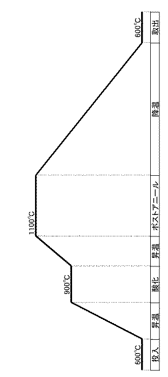
実施例1−6及び比較例1,2において、作製したSOIウェーハにRTA処理と犠牲酸化処理(熱酸化+HF溶液による熱酸化膜除去)を行った。条件を表1に示す。図2に実施例1の犠牲酸化処理における熱酸化の温度プロファイルを示す。
また、比較例3において、作製したSOIウェーハにRTA処理と犠牲酸化処理(熱酸化+HF溶液による熱酸化膜除去)を行ったが、第1及び第2の犠牲酸化処理では、熱酸化の終了後に連続的にポストアニール(100%Ar、1100℃、2時間)を実施した。図3に、比較例3の犠牲酸化処理における熱酸化及びポストアニールの温度プロファイルを示す。
比較例4では、第2のRTA処理の代わりにバッチ式熱処理炉によるArアニール(100%Ar、1200℃、1時間)を実施した。
In Example 1-6 and Comparative Examples 1 and 2, the fabricated SOI wafer was subjected to RTA treatment and sacrificial oxidation treatment (thermal oxidation + thermal oxide film removal using HF solution). The conditions are shown in Table 1. FIG. 2 shows a temperature profile of thermal oxidation in the sacrificial oxidation process of the first embodiment.
In Comparative Example 3, the manufactured SOI wafer was subjected to RTA treatment and sacrificial oxidation treatment (thermal oxidation + thermal oxide film removal by HF solution). In the first and second sacrificial oxidation treatments, after thermal oxidation was completed, Continuous post-annealing (100% Ar, 1100 ° C., 2 hours) was performed. FIG. 3 shows temperature profiles of thermal oxidation and post-annealing in the sacrificial oxidation treatment of Comparative Example 3.
In Comparative Example 4, Ar annealing (100% Ar, 1200 ° C., 1 hour) using a batch heat treatment furnace was performed instead of the second RTA treatment.
[エッチピット測定方法]
製造したSOIウェーハについて、クロムレスの選択エッチング液でSOI層表面を30nmエッチングし、光学顕微鏡でエッチピット密度を測定した。
[スリップ発生率]
各実施例、比較例の熱処理条件でSOIウェーハを100枚処理し、スリップ不良の限度見本と比較してスリップ不良と判断されたものの比率を調べた。
[表面粗さ]
第2の犠牲酸化処理後のSOI層表面をAFMにより測定した(測定領域30μm角)。
以上の評価結果を表1に示す。
[Etch pit measurement method]
With respect to the manufactured SOI wafer, the surface of the SOI layer was etched by 30 nm with a chromeless selective etching solution, and the etch pit density was measured with an optical microscope.
[Slip occurrence rate]
100 SOI wafers were processed under the heat treatment conditions of each of the examples and comparative examples, and the ratio of those judged to be slip failures was compared with the limit sample of slip failure.
[Surface roughness]
The surface of the SOI layer after the second sacrificial oxidation treatment was measured by AFM (
The above evaluation results are shown in Table 1.
実施例1〜6では、エッチピット、スリップ発生率、表面粗さのいずれも良好な結果となった。また、別途測定したSOI層の膜厚分布は、膜厚レンジ(面内の最大膜厚値から最小膜厚値を引いた値)が3nm以内の良好な膜厚均一性が得られていた。
なお、実施例5,6は、熱処理による剥離を行っているため、表面粗さが実施例1〜4に比べてやや大きな値となったが、剥離直後の表面粗さと比較すると十分に低減されており、エッチピット、スリップ発生率は、実施例1〜4と同等レベルであった。
In Examples 1 to 6, the etch pit, the slip occurrence rate, and the surface roughness were all good. Moreover, the film thickness distribution of the SOI layer measured separately showed that the film thickness range (a value obtained by subtracting the minimum film thickness value from the in-plane maximum film thickness value) was within 3 nm and good film thickness uniformity was obtained.
In Examples 5 and 6, since peeling was performed by heat treatment, the surface roughness was slightly larger than those in Examples 1 to 4, but was sufficiently reduced compared to the surface roughness immediately after peeling. The etch pit and slip occurrence rates were at the same level as in Examples 1 to 4.
比較例1では、犠牲酸化処理の熱酸化の温度が1000℃を超える温度であるため、酸化前のRTA処理で完全には除去できなかったダメージに起因するOSFが発生し、SOI層に欠陥(エッチピット)が多発した。
比較例2では、RTA処理の温度が1100℃未満であるため、ダメージの除去が不十分となり、950℃の熱酸化でもOSFが発生し、SOI層に欠陥(エッチピット)が多発した。
In Comparative Example 1, since the temperature of the thermal oxidation in the sacrificial oxidation process exceeds 1000 ° C., OSF due to damage that cannot be completely removed by the RTA process before oxidation occurs, and the SOI layer has defects ( Etch pits) occurred frequently.
In Comparative Example 2, since the temperature of the RTA treatment was less than 1100 ° C., damage removal was insufficient, OSF was generated even in thermal oxidation at 950 ° C., and defects (etch pits) occurred frequently in the SOI layer.
比較例3では、熱酸化の終了後に連続的に高温長時間のポストアニールを実施したため、スリップの発生率が悪化し、実施例1〜6の2倍程度となった。
比較例4では、第2のRTA処理の代わりにバッチ式熱処理炉による高温Arアニールを実施したため、更にスリップの発生率が悪化し、実施例1〜6に比べて2倍程度となった。
In Comparative Example 3, post-annealing at a high temperature and for a long time was continuously performed after the completion of thermal oxidation, so that the slip generation rate deteriorated and became about twice that of Examples 1-6.
In Comparative Example 4, since high-temperature Ar annealing was performed using a batch heat treatment furnace instead of the second RTA treatment, the slip generation rate further deteriorated, and was about twice that of Examples 1-6.
なお、本発明は、上記実施形態に限定されるものではない。上記実施形態は、例示であり、本発明の特許請求の範囲に記載された技術的思想と実質的に同一な構成を有し、同様な作用効果を奏するものは、いかなるものであっても本発明の技術的範囲に包含される。 The present invention is not limited to the above embodiment. The above-described embodiment is an exemplification, and the present invention has substantially the same configuration as the technical idea described in the claims of the present invention, and any device that exhibits the same function and effect is the present invention. It is included in the technical scope of the invention.
10…ボンドウェーハ、 11…ベースウェーハ、 12…酸化膜、
13…イオン注入層、 14…埋め込み酸化膜、 15…貼り合わせSOIウェーハ、
16…SOI層。
10 ... Bond wafer, 11 ... Base wafer, 12 ... Oxide film,
13 ... ion implantation layer, 14 ... buried oxide film, 15 ... bonded SOI wafer,
16 ... SOI layer.
Claims (4)
前記剥離後の貼り合わせSOIウェーハに対して、第1のRTA処理を行った後、第1の犠牲酸化処理を行い、その後、第2のRTA処理を行った後、第2の犠牲酸化処理を行う工程を有し、
前記第1及び第2のRTA処理を、水素ガス含有雰囲気下、1100℃以上の温度で行い、前記第1及び第2の犠牲酸化処理において、900℃以上1000℃以下の温度でバッチ式熱処理炉による熱酸化のみを行うことによって前記SOI層表面に熱酸化膜を形成した後、該熱酸化膜を除去する処理を行うことを特徴とする貼り合わせSOIウェーハの製造方法。 At least one kind of gas ion of hydrogen ion and rare gas ion is ion-implanted from the surface of the bond wafer made of silicon single crystal to form an ion-implanted layer inside the bond wafer, and on the ion-implanted side of the bond wafer. After bonding the surface and the surface of the base wafer through an insulating film, a part of the bond wafer is peeled off by the ion implantation layer to manufacture a bonded SOI wafer having an SOI layer on the base wafer. A method,
A first RTA process is performed on the bonded SOI wafer after peeling, and then a first sacrificial oxidation process is performed. Thereafter, a second RTA process is performed, and then a second sacrificial oxidation process is performed. A process of performing,
The first and second RTA processes are performed in a hydrogen gas-containing atmosphere at a temperature of 1100 ° C. or higher, and in the first and second sacrificial oxidation processes, a batch heat treatment furnace is operated at a temperature of 900 ° C. or higher and 1000 ° C. or lower. A method for producing a bonded SOI wafer, comprising: forming a thermal oxide film on the surface of the SOI layer by performing only thermal oxidation using a method, and then removing the thermal oxide film.
Priority Applications (6)
| Application Number | Priority Date | Filing Date | Title |
|---|---|---|---|
| JP2012001611A JP2013143407A (en) | 2012-01-06 | 2012-01-06 | Method of manufacturing laminated soi wafer |
| US14/364,162 US9076840B2 (en) | 2012-01-06 | 2012-11-30 | Method for manufacturing a bonded SOI wafer |
| KR1020147018404A KR20140121392A (en) | 2012-01-06 | 2012-11-30 | Method for manufacturing bonded silicon-on-insulator (soi) wafer |
| PCT/JP2012/007690 WO2013102968A1 (en) | 2012-01-06 | 2012-11-30 | Method for manufacturing bonded silicon-on-insulator (soi) wafer |
| CN201280065462.0A CN104025254A (en) | 2012-01-06 | 2012-11-30 | Method for manufacturing bonded silicon-on-insulator (SOI) wafer |
| EP12864102.4A EP2802001A4 (en) | 2012-01-06 | 2012-11-30 | Method for manufacturing bonded silicon-on-insulator (soi) wafer |
Applications Claiming Priority (1)
| Application Number | Priority Date | Filing Date | Title |
|---|---|---|---|
| JP2012001611A JP2013143407A (en) | 2012-01-06 | 2012-01-06 | Method of manufacturing laminated soi wafer |
Publications (1)
| Publication Number | Publication Date |
|---|---|
| JP2013143407A true JP2013143407A (en) | 2013-07-22 |
Family
ID=48745045
Family Applications (1)
| Application Number | Title | Priority Date | Filing Date |
|---|---|---|---|
| JP2012001611A Pending JP2013143407A (en) | 2012-01-06 | 2012-01-06 | Method of manufacturing laminated soi wafer |
Country Status (6)
| Country | Link |
|---|---|
| US (1) | US9076840B2 (en) |
| EP (1) | EP2802001A4 (en) |
| JP (1) | JP2013143407A (en) |
| KR (1) | KR20140121392A (en) |
| CN (1) | CN104025254A (en) |
| WO (1) | WO2013102968A1 (en) |
Cited By (3)
| Publication number | Priority date | Publication date | Assignee | Title |
|---|---|---|---|---|
| JP2014232806A (en) * | 2013-05-29 | 2014-12-11 | 信越半導体株式会社 | Method for manufacturing laminated wafer |
| JP2016082093A (en) * | 2014-10-17 | 2016-05-16 | 信越半導体株式会社 | Bonded wafer manufacturing method |
| KR20160134661A (en) | 2014-03-18 | 2016-11-23 | 신에쯔 한도타이 가부시키가이샤 | Method for manufacturing laminated wafer |
Families Citing this family (8)
| Publication number | Priority date | Publication date | Assignee | Title |
|---|---|---|---|---|
| JP6200273B2 (en) * | 2013-10-17 | 2017-09-20 | 信越半導体株式会社 | Manufacturing method of bonded wafer |
| JP6380245B2 (en) * | 2015-06-15 | 2018-08-29 | 信越半導体株式会社 | Manufacturing method of SOI wafer |
| JP6531743B2 (en) * | 2016-09-27 | 2019-06-19 | 信越半導体株式会社 | Method of manufacturing bonded SOI wafer |
| CN106601615B (en) * | 2016-12-27 | 2020-05-15 | 上海新傲科技股份有限公司 | Annealing method for improving bonding strength |
| FR3093860B1 (en) * | 2019-03-15 | 2021-03-05 | Soitec Silicon On Insulator | Method of transferring a useful layer onto a support substrate |
| FR3093858B1 (en) * | 2019-03-15 | 2021-03-05 | Soitec Silicon On Insulator | Method of transferring a useful layer onto a support substrate |
| CN116387241A (en) * | 2023-04-21 | 2023-07-04 | 中芯先锋集成电路制造(绍兴)有限公司 | Method for manufacturing semiconductor-on-insulator substrate and method for manufacturing semiconductor device |
| CN117096012B (en) * | 2023-08-22 | 2024-03-26 | 中环领先半导体科技股份有限公司 | Oxide film, silicon wafer and preparation method thereof |
Citations (3)
| Publication number | Priority date | Publication date | Assignee | Title |
|---|---|---|---|---|
| JP2003510799A (en) * | 1999-08-20 | 2003-03-18 | エス オー イ テク シリコン オン インシュレータ テクノロジース | Microelectronics substrate processing method and substrate obtained by the method |
| WO2007074550A1 (en) * | 2005-12-27 | 2007-07-05 | Shin-Etsu Chemical Co., Ltd. | Process for producing soi wafer and soi wafer |
| WO2010106101A1 (en) * | 2009-03-18 | 2010-09-23 | S.O.I.Tec Silicon On Insulator Technologies | Finishing method for a substrate of "silicon-on-insulator" soi type |
Family Cites Families (11)
| Publication number | Priority date | Publication date | Assignee | Title |
|---|---|---|---|---|
| FR2681472B1 (en) | 1991-09-18 | 1993-10-29 | Commissariat Energie Atomique | PROCESS FOR PRODUCING THIN FILMS OF SEMICONDUCTOR MATERIAL. |
| JPH11307472A (en) | 1998-04-23 | 1999-11-05 | Shin Etsu Handotai Co Ltd | Soi wafer and manufacture soi by hydrogen ion releasing method |
| JP2000124092A (en) | 1998-10-16 | 2000-04-28 | Shin Etsu Handotai Co Ltd | Manufacture of soi wafer by hydrogen-ion implantation stripping method and soi wafer manufactured thereby |
| KR100730806B1 (en) * | 1999-10-14 | 2007-06-20 | 신에쯔 한도타이 가부시키가이샤 | Method for manufacturing soi wafer, and soi wafer |
| US6884696B2 (en) | 2001-07-17 | 2005-04-26 | Shin-Etsu Handotai Co., Ltd. | Method for producing bonding wafer |
| KR20060030911A (en) | 2003-07-29 | 2006-04-11 | 에스. 오. 이. 떼끄 씰리꽁 오 냉쉴라또흐 떼끄놀로지 | Process for obtaining a thin layer of increased quality by co-implantation and thermal annealing |
| CN101027768B (en) | 2004-09-21 | 2010-11-03 | S.O.I.Tec绝缘体上硅技术公司 | Thin layer transfer method wherein a co-implantation step is performed according to conditions avoiding blisters formation and limiting roughness |
| JP2008526010A (en) | 2004-12-28 | 2008-07-17 | エス. オー. アイ. テック シリコン オン インシュレーター テクノロジーズ | Method for obtaining thin layers with low hole density |
| FR2895563B1 (en) * | 2005-12-22 | 2008-04-04 | Soitec Silicon On Insulator | METHOD FOR SIMPLIFYING A FINISHING SEQUENCE AND STRUCTURE OBTAINED BY THE METHOD |
| JP5135935B2 (en) * | 2007-07-27 | 2013-02-06 | 信越半導体株式会社 | Manufacturing method of bonded wafer |
| JP5263509B2 (en) * | 2008-09-19 | 2013-08-14 | 信越半導体株式会社 | Manufacturing method of bonded wafer |
-
2012
- 2012-01-06 JP JP2012001611A patent/JP2013143407A/en active Pending
- 2012-11-30 KR KR1020147018404A patent/KR20140121392A/en not_active Application Discontinuation
- 2012-11-30 EP EP12864102.4A patent/EP2802001A4/en not_active Withdrawn
- 2012-11-30 WO PCT/JP2012/007690 patent/WO2013102968A1/en active Application Filing
- 2012-11-30 CN CN201280065462.0A patent/CN104025254A/en active Pending
- 2012-11-30 US US14/364,162 patent/US9076840B2/en active Active
Patent Citations (3)
| Publication number | Priority date | Publication date | Assignee | Title |
|---|---|---|---|---|
| JP2003510799A (en) * | 1999-08-20 | 2003-03-18 | エス オー イ テク シリコン オン インシュレータ テクノロジース | Microelectronics substrate processing method and substrate obtained by the method |
| WO2007074550A1 (en) * | 2005-12-27 | 2007-07-05 | Shin-Etsu Chemical Co., Ltd. | Process for producing soi wafer and soi wafer |
| WO2010106101A1 (en) * | 2009-03-18 | 2010-09-23 | S.O.I.Tec Silicon On Insulator Technologies | Finishing method for a substrate of "silicon-on-insulator" soi type |
Cited By (4)
| Publication number | Priority date | Publication date | Assignee | Title |
|---|---|---|---|---|
| JP2014232806A (en) * | 2013-05-29 | 2014-12-11 | 信越半導体株式会社 | Method for manufacturing laminated wafer |
| KR20160134661A (en) | 2014-03-18 | 2016-11-23 | 신에쯔 한도타이 가부시키가이샤 | Method for manufacturing laminated wafer |
| US9773694B2 (en) | 2014-03-18 | 2017-09-26 | Shin-Etsu Handotai Co., Ltd. | Method for manufacturing bonded wafer |
| JP2016082093A (en) * | 2014-10-17 | 2016-05-16 | 信越半導体株式会社 | Bonded wafer manufacturing method |
Also Published As
| Publication number | Publication date |
|---|---|
| WO2013102968A1 (en) | 2013-07-11 |
| US20140322895A1 (en) | 2014-10-30 |
| CN104025254A (en) | 2014-09-03 |
| KR20140121392A (en) | 2014-10-15 |
| EP2802001A4 (en) | 2015-09-16 |
| US9076840B2 (en) | 2015-07-07 |
| EP2802001A1 (en) | 2014-11-12 |
Similar Documents
| Publication | Publication Date | Title |
|---|---|---|
| WO2013102968A1 (en) | Method for manufacturing bonded silicon-on-insulator (soi) wafer | |
| JP5673572B2 (en) | Manufacturing method of bonded SOI wafer | |
| JP4421652B2 (en) | Manufacturing method of SOI wafer | |
| JP2009032972A (en) | Method of manufacturing bonded wafer | |
| JP2006210899A (en) | Process for producing soi wafer, and soi wafer | |
| TWI573173B (en) | Method for manufacturing conformable SOI wafers | |
| TWI685019B (en) | Method for manufacturing silicon wafer on insulator | |
| JP2003347176A (en) | Manufacturing method of laminate wafer | |
| KR102095383B1 (en) | Method for manufacturing bonded wafer | |
| WO2016059748A1 (en) | Method for manufacturing bonded wafer | |
| JP2006202989A (en) | Soi wafer and manufacturing method therefor | |
| JP2009283582A (en) | Bonded wafer manufacturing method and bonded wafer | |
| JP6500845B2 (en) | Method of manufacturing bonded wafer | |
| JP5703920B2 (en) | Manufacturing method of bonded wafer | |
| KR20160013037A (en) | Method for manufacturing bonded wafer | |
| JP5673180B2 (en) | Manufacturing method of bonded wafer | |
| JP5368000B2 (en) | Manufacturing method of SOI substrate | |
| JP6136786B2 (en) | Manufacturing method of bonded wafer | |
| JP2014212172A (en) | Method of manufacturing laminated wafer |
Legal Events
| Date | Code | Title | Description |
|---|---|---|---|
| A621 | Written request for application examination |
Free format text: JAPANESE INTERMEDIATE CODE: A621 Effective date: 20131212 |
|
| A131 | Notification of reasons for refusal |
Free format text: JAPANESE INTERMEDIATE CODE: A131 Effective date: 20150217 |
|
| A521 | Written amendment |
Free format text: JAPANESE INTERMEDIATE CODE: A523 Effective date: 20150326 |
|
| A02 | Decision of refusal |
Free format text: JAPANESE INTERMEDIATE CODE: A02 Effective date: 20150616 |
|
| A521 | Written amendment |
Free format text: JAPANESE INTERMEDIATE CODE: A523 Effective date: 20150710 |
|
| A911 | Transfer to examiner for re-examination before appeal (zenchi) |
Free format text: JAPANESE INTERMEDIATE CODE: A911 Effective date: 20150818 |
|
| A912 | Re-examination (zenchi) completed and case transferred to appeal board |
Free format text: JAPANESE INTERMEDIATE CODE: A912 Effective date: 20151002 |