JP2012204666A - Solar cell module, manufacturing method of solar cell module, and tab line - Google Patents
Solar cell module, manufacturing method of solar cell module, and tab line Download PDFInfo
- Publication number
- JP2012204666A JP2012204666A JP2011068685A JP2011068685A JP2012204666A JP 2012204666 A JP2012204666 A JP 2012204666A JP 2011068685 A JP2011068685 A JP 2011068685A JP 2011068685 A JP2011068685 A JP 2011068685A JP 2012204666 A JP2012204666 A JP 2012204666A
- Authority
- JP
- Japan
- Prior art keywords
- solar cell
- tab
- wire
- electrode
- tab wire
- Prior art date
- Legal status (The legal status is an assumption and is not a legal conclusion. Google has not performed a legal analysis and makes no representation as to the accuracy of the status listed.)
- Granted
Links
- 238000004519 manufacturing process Methods 0.000 title claims description 16
- 239000012790 adhesive layer Substances 0.000 claims abstract description 68
- 230000002093 peripheral effect Effects 0.000 claims abstract description 31
- 239000000853 adhesive Substances 0.000 claims description 27
- 230000001070 adhesive effect Effects 0.000 claims description 26
- 239000010410 layer Substances 0.000 claims description 18
- 238000000034 method Methods 0.000 claims description 11
- 230000008569 process Effects 0.000 claims description 5
- 229920005989 resin Polymers 0.000 description 27
- 239000011347 resin Substances 0.000 description 27
- 239000002245 particle Substances 0.000 description 23
- RYGMFSIKBFXOCR-UHFFFAOYSA-N Copper Chemical compound [Cu] RYGMFSIKBFXOCR-UHFFFAOYSA-N 0.000 description 19
- 239000003822 epoxy resin Substances 0.000 description 15
- 229920000647 polyepoxide Polymers 0.000 description 15
- 238000006243 chemical reaction Methods 0.000 description 14
- 239000011230 binding agent Substances 0.000 description 12
- LNEPOXFFQSENCJ-UHFFFAOYSA-N haloperidol Chemical compound C1CC(O)(C=2C=CC(Cl)=CC=2)CCN1CCCC(=O)C1=CC=C(F)C=C1 LNEPOXFFQSENCJ-UHFFFAOYSA-N 0.000 description 12
- 239000002313 adhesive film Substances 0.000 description 11
- 239000011889 copper foil Substances 0.000 description 9
- 239000010408 film Substances 0.000 description 9
- 239000003795 chemical substances by application Substances 0.000 description 8
- 238000001723 curing Methods 0.000 description 8
- 230000000052 comparative effect Effects 0.000 description 7
- YXFVVABEGXRONW-UHFFFAOYSA-N Toluene Chemical compound CC1=CC=CC=C1 YXFVVABEGXRONW-UHFFFAOYSA-N 0.000 description 6
- 239000000463 material Substances 0.000 description 6
- 229910052782 aluminium Inorganic materials 0.000 description 5
- XAGFODPZIPBFFR-UHFFFAOYSA-N aluminium Chemical compound [Al] XAGFODPZIPBFFR-UHFFFAOYSA-N 0.000 description 5
- 239000011521 glass Substances 0.000 description 5
- 238000010438 heat treatment Methods 0.000 description 5
- PXHVJJICTQNCMI-UHFFFAOYSA-N Nickel Chemical compound [Ni] PXHVJJICTQNCMI-UHFFFAOYSA-N 0.000 description 4
- BQCADISMDOOEFD-UHFFFAOYSA-N Silver Chemical compound [Ag] BQCADISMDOOEFD-UHFFFAOYSA-N 0.000 description 4
- 239000005038 ethylene vinyl acetate Substances 0.000 description 4
- PCHJSUWPFVWCPO-UHFFFAOYSA-N gold Chemical compound [Au] PCHJSUWPFVWCPO-UHFFFAOYSA-N 0.000 description 4
- 239000011256 inorganic filler Substances 0.000 description 4
- 229910003475 inorganic filler Inorganic materials 0.000 description 4
- 239000004850 liquid epoxy resins (LERs) Substances 0.000 description 4
- 229920001200 poly(ethylene-vinyl acetate) Polymers 0.000 description 4
- 229920000139 polyethylene terephthalate Polymers 0.000 description 4
- 239000005020 polyethylene terephthalate Substances 0.000 description 4
- 238000005096 rolling process Methods 0.000 description 4
- 230000035939 shock Effects 0.000 description 4
- 229910052709 silver Inorganic materials 0.000 description 4
- 239000004332 silver Substances 0.000 description 4
- 239000002904 solvent Substances 0.000 description 4
- 239000000758 substrate Substances 0.000 description 4
- XEKOWRVHYACXOJ-UHFFFAOYSA-N Ethyl acetate Chemical compound CCOC(C)=O XEKOWRVHYACXOJ-UHFFFAOYSA-N 0.000 description 3
- -1 Poly Ethylene Terephthalate Polymers 0.000 description 3
- 239000006087 Silane Coupling Agent Substances 0.000 description 3
- 229910052737 gold Inorganic materials 0.000 description 3
- 239000010931 gold Substances 0.000 description 3
- 239000011159 matrix material Substances 0.000 description 3
- 239000000203 mixture Substances 0.000 description 3
- 230000009467 reduction Effects 0.000 description 3
- 238000007650 screen-printing Methods 0.000 description 3
- 229910000679 solder Inorganic materials 0.000 description 3
- VTYYLEPIZMXCLO-UHFFFAOYSA-L Calcium carbonate Chemical compound [Ca+2].[O-]C([O-])=O VTYYLEPIZMXCLO-UHFFFAOYSA-L 0.000 description 2
- UFWIBTONFRDIAS-UHFFFAOYSA-N Naphthalene Chemical compound C1=CC=CC2=CC=CC=C21 UFWIBTONFRDIAS-UHFFFAOYSA-N 0.000 description 2
- VYPSYNLAJGMNEJ-UHFFFAOYSA-N Silicium dioxide Chemical compound O=[Si]=O VYPSYNLAJGMNEJ-UHFFFAOYSA-N 0.000 description 2
- 229910021417 amorphous silicon Inorganic materials 0.000 description 2
- 230000015572 biosynthetic process Effects 0.000 description 2
- DQXBYHZEEUGOBF-UHFFFAOYSA-N but-3-enoic acid;ethene Chemical compound C=C.OC(=O)CC=C DQXBYHZEEUGOBF-UHFFFAOYSA-N 0.000 description 2
- 239000004020 conductor Substances 0.000 description 2
- 229910021419 crystalline silicon Inorganic materials 0.000 description 2
- ZUOUZKKEUPVFJK-UHFFFAOYSA-N diphenyl Chemical compound C1=CC=CC=C1C1=CC=CC=C1 ZUOUZKKEUPVFJK-UHFFFAOYSA-N 0.000 description 2
- 230000005611 electricity Effects 0.000 description 2
- 238000007731 hot pressing Methods 0.000 description 2
- 238000010030 laminating Methods 0.000 description 2
- 229910052751 metal Inorganic materials 0.000 description 2
- 239000002184 metal Substances 0.000 description 2
- 239000002923 metal particle Substances 0.000 description 2
- 229910052759 nickel Inorganic materials 0.000 description 2
- 239000005026 oriented polypropylene Substances 0.000 description 2
- 239000013034 phenoxy resin Substances 0.000 description 2
- 229920006287 phenoxy resin Polymers 0.000 description 2
- 239000004033 plastic Substances 0.000 description 2
- 229920003023 plastic Polymers 0.000 description 2
- 229920001343 polytetrafluoroethylene Polymers 0.000 description 2
- 239000004810 polytetrafluoroethylene Substances 0.000 description 2
- 230000001681 protective effect Effects 0.000 description 2
- 239000012945 sealing adhesive Substances 0.000 description 2
- 239000003566 sealing material Substances 0.000 description 2
- 238000005476 soldering Methods 0.000 description 2
- 229920001187 thermosetting polymer Polymers 0.000 description 2
- 239000010409 thin film Substances 0.000 description 2
- KJCVRFUGPWSIIH-UHFFFAOYSA-N 1-naphthol Chemical compound C1=CC=C2C(O)=CC=CC2=C1 KJCVRFUGPWSIIH-UHFFFAOYSA-N 0.000 description 1
- HECLRDQVFMWTQS-RGOKHQFPSA-N 1755-01-7 Chemical compound C1[C@H]2[C@@H]3CC=C[C@@H]3[C@@H]1C=C2 HECLRDQVFMWTQS-RGOKHQFPSA-N 0.000 description 1
- 239000004925 Acrylic resin Substances 0.000 description 1
- 229920000178 Acrylic resin Polymers 0.000 description 1
- 229930185605 Bisphenol Natural products 0.000 description 1
- RWSOTUBLDIXVET-UHFFFAOYSA-N Dihydrogen sulfide Chemical class S RWSOTUBLDIXVET-UHFFFAOYSA-N 0.000 description 1
- 239000004593 Epoxy Substances 0.000 description 1
- ISWSIDIOOBJBQZ-UHFFFAOYSA-N Phenol Chemical compound OC1=CC=CC=C1 ISWSIDIOOBJBQZ-UHFFFAOYSA-N 0.000 description 1
- BLRPTPMANUNPDV-UHFFFAOYSA-N Silane Chemical compound [SiH4] BLRPTPMANUNPDV-UHFFFAOYSA-N 0.000 description 1
- XUIMIQQOPSSXEZ-UHFFFAOYSA-N Silicon Chemical compound [Si] XUIMIQQOPSSXEZ-UHFFFAOYSA-N 0.000 description 1
- PJANXHGTPQOBST-VAWYXSNFSA-N Stilbene Natural products C=1C=CC=CC=1/C=C/C1=CC=CC=C1 PJANXHGTPQOBST-VAWYXSNFSA-N 0.000 description 1
- GWEVSGVZZGPLCZ-UHFFFAOYSA-N Titan oxide Chemical compound O=[Ti]=O GWEVSGVZZGPLCZ-UHFFFAOYSA-N 0.000 description 1
- 238000003848 UV Light-Curing Methods 0.000 description 1
- LEVVHYCKPQWKOP-UHFFFAOYSA-N [Si].[Ge] Chemical compound [Si].[Ge] LEVVHYCKPQWKOP-UHFFFAOYSA-N 0.000 description 1
- 239000000654 additive Substances 0.000 description 1
- 230000000996 additive effect Effects 0.000 description 1
- 230000002411 adverse Effects 0.000 description 1
- 150000001412 amines Chemical class 0.000 description 1
- 239000004305 biphenyl Substances 0.000 description 1
- 235000010290 biphenyl Nutrition 0.000 description 1
- IISBACLAFKSPIT-UHFFFAOYSA-N bisphenol A Chemical compound C=1C=C(O)C=CC=1C(C)(C)C1=CC=C(O)C=C1 IISBACLAFKSPIT-UHFFFAOYSA-N 0.000 description 1
- 229910000019 calcium carbonate Inorganic materials 0.000 description 1
- 125000001951 carbamoylamino group Chemical group C(N)(=O)N* 0.000 description 1
- 239000011248 coating agent Substances 0.000 description 1
- 238000000576 coating method Methods 0.000 description 1
- 150000001875 compounds Chemical class 0.000 description 1
- 239000010949 copper Substances 0.000 description 1
- 229910052802 copper Inorganic materials 0.000 description 1
- 230000008878 coupling Effects 0.000 description 1
- 238000010168 coupling process Methods 0.000 description 1
- 238000005859 coupling reaction Methods 0.000 description 1
- 239000013039 cover film Substances 0.000 description 1
- 230000007547 defect Effects 0.000 description 1
- 238000010586 diagram Methods 0.000 description 1
- 238000007865 diluting Methods 0.000 description 1
- 238000004090 dissolution Methods 0.000 description 1
- 230000004907 flux Effects 0.000 description 1
- 239000011888 foil Substances 0.000 description 1
- 238000013007 heat curing Methods 0.000 description 1
- 150000002460 imidazoles Chemical class 0.000 description 1
- 229910010272 inorganic material Inorganic materials 0.000 description 1
- 239000011147 inorganic material Substances 0.000 description 1
- 238000003475 lamination Methods 0.000 description 1
- 239000004849 latent hardener Substances 0.000 description 1
- 239000000395 magnesium oxide Substances 0.000 description 1
- CPLXHLVBOLITMK-UHFFFAOYSA-N magnesium oxide Inorganic materials [Mg]=O CPLXHLVBOLITMK-UHFFFAOYSA-N 0.000 description 1
- AXZKOIWUVFPNLO-UHFFFAOYSA-N magnesium;oxygen(2-) Chemical compound [O-2].[Mg+2] AXZKOIWUVFPNLO-UHFFFAOYSA-N 0.000 description 1
- 238000005259 measurement Methods 0.000 description 1
- 229910021424 microcrystalline silicon Inorganic materials 0.000 description 1
- 239000012046 mixed solvent Substances 0.000 description 1
- 238000012986 modification Methods 0.000 description 1
- 230000004048 modification Effects 0.000 description 1
- 229910021421 monocrystalline silicon Inorganic materials 0.000 description 1
- 229920003986 novolac Polymers 0.000 description 1
- 239000011368 organic material Substances 0.000 description 1
- 239000003960 organic solvent Substances 0.000 description 1
- 238000007747 plating Methods 0.000 description 1
- 238000003825 pressing Methods 0.000 description 1
- 239000002096 quantum dot Substances 0.000 description 1
- 239000011342 resin composition Substances 0.000 description 1
- RXFVKZHOXNKNEU-UHFFFAOYSA-N s-(aminodisulfanyl)thiohydroxylamine Chemical compound NSSSN RXFVKZHOXNKNEU-UHFFFAOYSA-N 0.000 description 1
- 150000003839 salts Chemical class 0.000 description 1
- 238000007789 sealing Methods 0.000 description 1
- 229910000077 silane Inorganic materials 0.000 description 1
- 229910052710 silicon Inorganic materials 0.000 description 1
- 239000010703 silicon Substances 0.000 description 1
- 239000000377 silicon dioxide Substances 0.000 description 1
- 238000004544 sputter deposition Methods 0.000 description 1
- PJANXHGTPQOBST-UHFFFAOYSA-N stilbene Chemical compound C=1C=CC=CC=1C=CC1=CC=CC=C1 PJANXHGTPQOBST-UHFFFAOYSA-N 0.000 description 1
- 235000021286 stilbenes Nutrition 0.000 description 1
- 239000000454 talc Substances 0.000 description 1
- 229910052623 talc Inorganic materials 0.000 description 1
- 229920002803 thermoplastic polyurethane Polymers 0.000 description 1
- OGIDPMRJRNCKJF-UHFFFAOYSA-N titanium oxide Inorganic materials [Ti]=O OGIDPMRJRNCKJF-UHFFFAOYSA-N 0.000 description 1
- AAAQKTZKLRYKHR-UHFFFAOYSA-N triphenylmethane Chemical compound C1=CC=CC=C1C(C=1C=CC=CC=1)C1=CC=CC=C1 AAAQKTZKLRYKHR-UHFFFAOYSA-N 0.000 description 1
Images


Classifications
-
- H—ELECTRICITY
- H01—ELECTRIC ELEMENTS
- H01L—SEMICONDUCTOR DEVICES NOT COVERED BY CLASS H10
- H01L31/00—Semiconductor devices sensitive to infrared radiation, light, electromagnetic radiation of shorter wavelength or corpuscular radiation and specially adapted either for the conversion of the energy of such radiation into electrical energy or for the control of electrical energy by such radiation; Processes or apparatus specially adapted for the manufacture or treatment thereof or of parts thereof; Details thereof
- H01L31/04—Semiconductor devices sensitive to infrared radiation, light, electromagnetic radiation of shorter wavelength or corpuscular radiation and specially adapted either for the conversion of the energy of such radiation into electrical energy or for the control of electrical energy by such radiation; Processes or apparatus specially adapted for the manufacture or treatment thereof or of parts thereof; Details thereof adapted as photovoltaic [PV] conversion devices
- H01L31/042—PV modules or arrays of single PV cells
- H01L31/05—Electrical interconnection means between PV cells inside the PV module, e.g. series connection of PV cells
- H01L31/0504—Electrical interconnection means between PV cells inside the PV module, e.g. series connection of PV cells specially adapted for series or parallel connection of solar cells in a module
- H01L31/0512—Electrical interconnection means between PV cells inside the PV module, e.g. series connection of PV cells specially adapted for series or parallel connection of solar cells in a module made of a particular material or composition of materials
-
- Y—GENERAL TAGGING OF NEW TECHNOLOGICAL DEVELOPMENTS; GENERAL TAGGING OF CROSS-SECTIONAL TECHNOLOGIES SPANNING OVER SEVERAL SECTIONS OF THE IPC; TECHNICAL SUBJECTS COVERED BY FORMER USPC CROSS-REFERENCE ART COLLECTIONS [XRACs] AND DIGESTS
- Y02—TECHNOLOGIES OR APPLICATIONS FOR MITIGATION OR ADAPTATION AGAINST CLIMATE CHANGE
- Y02E—REDUCTION OF GREENHOUSE GAS [GHG] EMISSIONS, RELATED TO ENERGY GENERATION, TRANSMISSION OR DISTRIBUTION
- Y02E10/00—Energy generation through renewable energy sources
- Y02E10/50—Photovoltaic [PV] energy
Landscapes
- Life Sciences & Earth Sciences (AREA)
- Sustainable Development (AREA)
- Physics & Mathematics (AREA)
- Condensed Matter Physics & Semiconductors (AREA)
- Electromagnetism (AREA)
- General Physics & Mathematics (AREA)
- Engineering & Computer Science (AREA)
- Computer Hardware Design (AREA)
- Microelectronics & Electronic Packaging (AREA)
- Power Engineering (AREA)
- Photovoltaic Devices (AREA)
Abstract
Description
本発明は、タブ線によって複数の太陽電池セルが接続された太陽電池モジュールに関し、特に線状のタブ線、このタブ線を用いた太陽電池モジュール及び太陽電池モジュールの製造方法に関するものである。 The present invention relates to a solar cell module in which a plurality of solar cells are connected by a tab wire, and particularly to a linear tab wire, a solar cell module using the tab wire, and a method for manufacturing the solar cell module.
例えば結晶シリコン系太陽電池モジュールでは、複数の隣接する太陽電池セルが、インターコネクタとなるタブ線により接続されている。タブ線は、その一端側を一の太陽電池セルの表面電極に接続され、他端側を隣接する太陽電池セルの裏面電極に接続することにより、各太陽電池セルを直列に接続する。このとき、タブ線は、一端側の一面側が一の太陽電池セルの表面電極に接着され、他端側の他面側が隣接する太陽電池セルの裏面電極に接着されている。 For example, in a crystalline silicon-based solar battery module, a plurality of adjacent solar battery cells are connected by tab wires serving as interconnectors. One end side of the tab wire is connected to the front surface electrode of one solar battery cell, and the other end side is connected to the back surface electrode of the adjacent solar battery cell, thereby connecting the solar battery cells in series. At this time, one surface of the tab wire is bonded to the surface electrode of one solar cell, and the other surface of the other end is bonded to the back electrode of the adjacent solar cell.
具体的に、太陽電池セルは、受光面に銀ペーストのスクリーン印刷によりバスバー電極が形成され、太陽電池セルの裏面接続部にAg電極が形成されている。なお、太陽電池セル裏面の接続部以外の領域はAl電極やAg電極が形成されている。 Specifically, in the solar battery cell, a bus bar electrode is formed by screen printing of silver paste on the light receiving surface, and an Ag electrode is formed on the back surface connection portion of the solar battery cell. In addition, Al electrodes and Ag electrodes are formed in regions other than the connection portion on the back surface of the solar battery cell.
また、図11に示すように、タブ線50は、リボン状銅箔51の両面にハンダコート層52が設けられることにより形成される。具体的に、タブ線は、厚さ0.05〜0.2mm程度に圧延した銅箔をスリットし、あるいは銅ワイヤーを平板状に圧延するなどして得た幅1〜3mmの平角銅線に、ハンダメッキやディップハンダ付け等を施すことにより形成される。
As shown in FIG. 11, the
太陽電池セルとタブ線との接続は、タブ線を太陽電池セルの各電極上に配置し、加熱ボンダーによって熱加圧することにより、タブ線表面に形成したハンダを溶融、冷却することにより行う(特許文献1)。 The connection between the solar battery cell and the tab wire is performed by disposing the tab wire on each electrode of the solar battery cell and applying heat and pressure with a heating bonder to melt and cool the solder formed on the tab wire surface ( Patent Document 1).
しかし、半田付けでは約260℃と高温による接続処理が行われるため、太陽電池セルの反りや、タブ線と表面電極及び裏面電極との接続部に生じる内部応力、さらにフラックスの残渣等により、太陽電池セルの表面電極及び裏面電極とタブ線との間の接続信頼性が低下することが懸念される。 However, since soldering is performed at a high temperature of about 260 ° C., the solar cells are warped, the internal stress generated at the connection between the tab wire and the front and back electrodes, the residue of the flux, etc. There is a concern that the connection reliability between the front and back electrodes of the battery cell and the tab wire is lowered.
そこで、従来、太陽電池セルの表面電極及び裏面電極とタブ線との接続に、比較的低い温度での熱圧着処理による接続が可能な導電性接着フィルムが使用されている(特許文献2)。このような導電性接着フィルムとしては、平均粒径が数μmオーダーの球状または鱗片状の導電性粒子を熱硬化型バインダー樹脂組成物に分散してフィルム化したものが使用されている。 Therefore, conventionally, a conductive adhesive film that can be connected by thermocompression treatment at a relatively low temperature is used for connection between the front and back electrodes of the solar battery cell and the tab wire (Patent Document 2). As such a conductive adhesive film, a film obtained by dispersing spherical or scaly conductive particles having an average particle size on the order of several μm in a thermosetting binder resin composition is used.
導電性接着フィルムは、表面電極及び裏面電極とタブ線との間に介在された後、タブ線の上から加熱ボンダーによって熱加圧されることにより、バインダー樹脂が流動性を示して電極、タブ線間より流出されるとともに、導電性粒子が電極とタブ線間の導通を図り、この状態でバインダー樹脂が熱硬化する。これにより、タブ線によって複数の太陽電池セルが直列接続されたストリングスが形成される。 The conductive adhesive film is interposed between the front electrode and the back electrode and the tab wire, and then thermally pressed by a heating bonder from above the tab wire, so that the binder resin exhibits fluidity and the electrode and tab. While flowing out from between the wires, the conductive particles conduct between the electrode and the tab wire, and in this state, the binder resin is thermally cured. Thereby, the string by which the several photovoltaic cell was connected in series by the tab wire is formed.
導電性接着フィルムを用いてタブ線と表面電極及び裏面電極とが接続された複数の太陽電池セルは、ガラス、透光性プラスチックなどの透光性を有する表面保護材と、PET(Poly Ethylene Terephthalate)等のフィルムからなる背面保護材との間に、エチレンビニルアセテート樹脂(EVA)等の透光性を有する封止材により封止される。 A plurality of solar cells in which a tab wire and a front electrode and a back electrode are connected using a conductive adhesive film are made of a surface protective material having translucency such as glass and translucent plastic, and PET (Poly Ethylene Terephthalate). ) And the like, and a back protective material made of a film such as ethylene vinyl acetate resin (EVA).
しかし、上述したように、タブ線は、厚さ0.05〜0.2mm程度に圧延した銅箔をスリットし、あるいは銅ワイヤーを平板状に圧延するなどして、平角銅線を形成する必要があり、製造工数が増える。 However, as described above, the tab wire needs to be formed into a flat copper wire by slitting a copper foil rolled to a thickness of about 0.05 to 0.2 mm or rolling a copper wire into a flat plate shape. And manufacturing man-hours increase.
また、平角導線からなるタブ線は、幅2〜3mm程度の幅を有し、これを太陽電池セルの受光面に接着した場合、タブ線の幅に応じたシャドーロスが発生してしまう。 Moreover, the tab wire which consists of a rectangular conducting wire has a width | variety of about 2-3 mm in width, and when this is adhere | attached on the light-receiving surface of a photovoltaic cell, the shadow loss according to the width | variety of a tab wire will generate | occur | produce.
そこで、本発明は、製造が容易で、またシャドーロスの低減を図ることができるタブ線、当該タブ線を用いた太陽電池セル及び太陽電池モジュールの製造方法を提供することを目的とする。 Then, an object of this invention is to provide the manufacturing method of the tab wire which can be manufactured easily and can aim at reduction of a shadow loss, the photovoltaic cell using the said tab wire, and a solar cell module.
上述した課題を解決するために、本発明に係る太陽電池モジュールは、複数の太陽電池セルと、上記太陽電池セルの表面及び隣接する太陽電池セルの裏面にそれぞれ形成された電極上に接着され、複数の上記太陽電池セル同士を接続するタブ線とを備え、上記タブ線は、線状をなし、上記電極との接着部を含む外周面を覆う接着剤層によって上記電極と接着されているものである。 In order to solve the above-described problem, the solar cell module according to the present invention is bonded to a plurality of solar cells and electrodes formed on the surface of the solar cell and the back surface of the adjacent solar cell, A plurality of tab wires connecting the plurality of solar cells, and the tab wires are linearly bonded to the electrodes by an adhesive layer covering an outer peripheral surface including an adhesive portion with the electrodes. It is.
また、本発明に係る太陽電池モジュールの製造方法は、線状のタブ線を用い、太陽電池セルの表面電極に上記タブ線の一端側を配置し、上記太陽電池セルと隣接する太陽電池セルの裏面電極に上記タブ線の他端側を配置する工程と、上記タブ線を上記表面電極及び上記裏面電極へ熱加圧し、上記表面電極及び上記裏面電極と上記タブ線との間に流動した接着剤層によって上記タブ線を上記表面電極及び上記裏面電極へ接着する工程とを有するものである。 Moreover, the manufacturing method of the solar cell module which concerns on this invention uses a linear tab wire, arrange | positions the one end side of the said tab wire in the surface electrode of a photovoltaic cell, and the photovoltaic cell adjacent to the said photovoltaic cell The step of arranging the other end side of the tab wire on the back electrode, and the pressure bonding of the tab wire to the surface electrode and the back electrode, and flowing between the surface electrode and the back electrode and the tab wire A step of adhering the tab wire to the front electrode and the back electrode by an agent layer.
また、本発明に係るタブ線は、太陽電池セルの表面及び隣接する太陽電池セルの裏面にそれぞれ形成された電極上に接着され、複数の上記太陽電池セル同士を接続するタブ線において、線状をなし、長手方向に亘って少なくとも外周面の50%が接着剤層によって覆われ、上記接着剤層によって上記電極と接着されるものである。 Further, the tab wire according to the present invention is bonded to the electrodes formed on the front surface of the solar battery cell and the back surface of the adjacent solar battery cell, and the tab wire connecting the plurality of solar battery cells is linear. In the longitudinal direction, at least 50% of the outer peripheral surface is covered with the adhesive layer, and is bonded to the electrode by the adhesive layer.
本発明によれば、線状のタブ線を用いることにより、圧延銅箔を形成しスリットする工程や、銅線を平板状に圧延する工程が不要となり、製造設備や工数の削減を図ることができ、また、製造コストを抑えることもできる。また、本発明によれば、線状のタブ線を用いることにより、平板状のタブ線を用いた場合に比して、太陽電池セルの受光面に載置される面積を狭小化することができ、シャドーロスによる光電変換効率の低減を抑えることができる。 According to the present invention, by using a linear tab wire, a step of forming and slitting a rolled copper foil and a step of rolling a copper wire into a flat plate shape are not required, and it is possible to reduce manufacturing equipment and man-hours. In addition, the manufacturing cost can be reduced. Further, according to the present invention, by using a linear tab wire, the area placed on the light receiving surface of the solar battery cell can be reduced as compared with the case where a flat tab wire is used. And reduction in photoelectric conversion efficiency due to shadow loss can be suppressed.
以下、本発明が適用されたタブ線、このタブ線を用いた太陽電池モジュール及び太陽電池モジュールの製造方法について、図面を参照しながら詳細に説明する。なお、本発明は、以下の実施形態のみに限定されるものではなく、本発明の趣旨を逸脱しない範囲内において種々の変更が可能であることは勿論である。 Hereinafter, a tab wire to which the present invention is applied, a solar cell module using the tab wire, and a method for manufacturing the solar cell module will be described in detail with reference to the drawings. It should be noted that the present invention is not limited to the following embodiments, and various modifications can be made without departing from the spirit of the present invention.
[太陽電池モジュール]
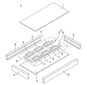
本発明が適用された太陽電池モジュール1は、図1〜図3に示すように、複数の太陽電池セル2がインターコネクタとなるタブ線3によって直列に接続されたストリングス4を有し、このストリングス4を複数配列したマトリクス5を備える。そして、太陽電池モジュール1は、このマトリクス5が封止接着剤のシート6で挟まれ、受光面側に設けられた表面カバー7及び裏面側に設けられたバックシート8とともに一括してラミネートされ、最後に、周囲にアルミニウムなどの金属フレーム9が取り付けられることにより形成される。
[Solar cell module]
The solar cell module 1 to which the present invention is applied has a string 4 in which a plurality of
封止接着剤としては、例えばエチレンビニルアセテート樹脂(EVA)等の透光性封止材が用いられる。また、表面カバー7としては、例えば、ガラスや透光性プラスチック等の透光性の材料が用いられる。また、バックシート8としては、ガラスやアルミニウム箔を樹脂フィルムで挟持した積層体等が用いられる。
As the sealing adhesive, for example, a translucent sealing material such as ethylene vinyl acetate resin (EVA) is used. Moreover, as the
太陽電池モジュールの各太陽電池セル2は、光電変換素子10を有する。光電変換素子10は、単結晶型シリコン光電変換素子、多結晶型光電変換素子を用いる結晶シリコン系太陽電池や、アモルファスシリコンからなるセルと微結晶シリコンやアモルファスシリコンゲルマニウムからなるセルとを積層させた光電変換素子を用いた薄膜シリコン系太陽電池、いわゆる化合物薄膜系、有機系、量子ドット型など、各種光電変換素子10を用いることができる。
Each
また、光電変換素子10は、受光面側に内部で発生した電気を集電するフィンガー電極12とフィンガー電極12の電気を集電するバスバー電極11とが設けられている。バスバー電極11及びフィンガー電極12は、太陽電池セル2の受光面となる表面にAgペーストがスクリーン印刷等により塗布された後、焼成されることにより形成される。また、フィンガー電極12は、受光面の全面に亘って、例えば約50〜200μm程度の幅を有するラインが、所定間隔、例えば2mmおきに、ほぼ平行に複数形成されている。バスバー電極11は、フィンガー電極12と略直交するように形成され、また、太陽電池セル2の面積に応じて複数形成されている。
Further, the
また、光電変換素子10は、受光面と反対の裏面側に、アルミニウムや銀からなる裏面電極13が設けられている。裏面電極13は、図2及び図3に示すように、アルミニウムや銀からなる電極が例えばスクリーン印刷やスパッタ等により太陽電池セル2の裏面に形成される。裏面電極13は、後述するタブ線3が接続されるタブ線接続部14を有する。
Further, the
そして、太陽電池セル2は、タブ線3によって、表面に形成された各バスバー電極11と、隣接する太陽電池セル2の裏面電極13とが電気的に接続され、これにより直列に接続されたストリングス4を構成する。タブ線3とバスバー電極11及び裏面電極13とは、タブ線3の外周面に設けられた接着剤層16によって接続される。
The
[タブ線]
タブ線3は、図2に示すように、隣接する太陽電池セル2X、2Y、2Zの各間を電気的に接続するものであり、図4に示すように、例えば、直径が0.2mm〜2.0mの線材15を備え、線材15の外周面には太陽電池セル2のバスバー電極11や裏面電極13との接着を図る接着剤層16が設けられている。
[Tab line]
As shown in FIG. 2, the
線材15は、線状の導電材からなり、例えば銅ワイヤーや金ワイヤー、アルミワイヤーなどの導電性を有する材料が用いられる。太陽電池モジュール1は、タブ線3として、線状の導電性のワイヤーからなる線材15を用いることにより、圧延銅箔を形成しスリットする工程や、銅線を平板状に圧延する工程が不要となり、製造設備や工数の削減を図ることができ、また、製造コストを抑えることもできる。また、太陽電池モジュール1は、タブ線3として、線材15を用いることにより、平板状のタブ線を用いた場合に比して、太陽電池セル2の受光面に載置される面積を狭小化することができ、シャドーロスによる光電変換効率の低減を抑えることができる。
The
[断面積]
線材15は、断面積が0.5〜13.0mm2の範囲のものを用いる。これは、太陽電池モジュール1は、タブ線3を介して各太陽電池セル2を電気的に接続するものであるため、線材15の断面積が0.5mm2よりも小さいとタブ線3の導通抵抗が高くなり、光電変換効率が低減するおそれがあるためである。また、太陽電池モジュール1は、タブ線3が太陽電池セル2の受光面に接着されるため、線材15の断面積が13.0mm2よりも大きくなると、タブ線3によるシャドーロスの影響が大きくなるおそれがあるためである。
[Cross sectional area]
[楕円形]
また、線材15は、断面が円形又は楕円形のものを用いることができる。この場合、図5に示すように、線材15は、断面を構成する円(楕円)の中心を通る直交座標のx軸(長軸)の半径をb、y軸(短軸)の半径をaとした場合、以下の関係を満たす。
0.4≦a≦2 (単位mm)
a≦b≦2 (単位mm)
これにより、タブ線3は、上述した断面積の範囲を満たし、導通抵抗の上昇やシャドーロスの影響を抑えることができる。
[Oblong]
Further, the
0.4 ≦ a ≦ 2 (Unit: mm)
a ≦ b ≦ 2 (unit: mm)
As a result, the
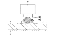
[接着剤層]
接着剤層16は、線材15の外周面を覆うことにより、タブ線3を太陽電池セル2のバスバー電極11や裏面電極13に接着させるものである。接着剤層16は、図6(a)(b)に示すように、ペースト状に形成し、予めタブ線3の線材15の外周面を被覆してもよく、あるいはフィルム状に形成し、太陽電池セル2の各電極11,13にタブ線3を接着させる際に、電極11,13上に配置し、線材15をこの接着フィルム上に配置した後、加熱ボンダー20により加熱押圧することにより線材15の外周面を被覆してもよい(図4)。また、太陽電池セル2に未硬化の接着剤層16、封止材を積層させ、ラミネート工程にて接着層16を硬化させる一括接続方法を用いることもできる。
[Adhesive layer]
The
接着剤層16は、図7に示すように、導電性粒子23が高密度に含有された熱硬化性のバインダー樹脂層である。また、接着剤層16は、押し込み性の観点から、バインダー樹脂の最低溶融粘度が、100〜100000Pa・sであることが好ましい。接着剤層16は、最低溶融粘度が低すぎると低圧着から本硬化の過程で樹脂が流動してしまい接続不良やセル受光面へのはみ出しが生じやすく、受光率低下の原因ともなる。また、最低溶融粘度が高すぎてもフィルム貼着時に不良を発生しやすく、接続信頼性に悪影響が出る場合もある。なお、最低溶融粘度については、サンプルを所定量回転式粘度計に装填し、所定の昇温速度で上昇させながら測定することができる。
As shown in FIG. 7, the
接着剤層16に用いられる導電性粒子23としては、特に制限されず、例えば、ニッケル、金、銀、銅などの金属粒子、樹脂粒子に金めっきなどを施したもの、樹脂粒子に金めっきを施した粒子の最外層に絶縁被覆を施したものなどを挙げることができる。なお、導電性粒子23として、扁平なフレーク状金属粒子を含有することにより、互いに重なり合う導電性粒子23の数を増加させ、良好な導通信頼性を確保することができる。
The
また、接着剤層16は、常温付近での粘度が10〜10000kPa・sであることが好ましく、さらに好ましくは、10〜5000kPa・sである。接着剤層16の粘度が10〜10000kPa・sの範囲であることにより、接着剤層16をテープ状のリール巻とした場合において、いわゆるはみ出しを防止することができ、また、所定のタック力を維持することができる。
The
接着剤層16のバインダー樹脂層の組成は、上述のような特徴を害さない限り、特に制限されないが、より好ましくは、膜形成樹脂と、液状エポキシ樹脂と、潜在性硬化剤と、シランカップリング剤とを含有する。
The composition of the binder resin layer of the
膜形成樹脂は、平均分子量が10000以上の高分子量樹脂に相当し、フィルム形成性の観点から、10000〜80000程度の平均分子量であることが好ましい。膜形成樹脂としては、エポキシ樹脂、変性エポキシ樹脂、ウレタン樹脂、フェノキシ樹脂等の種々の樹脂を使用することができ、その中でも膜形成状態、接続信頼性等の観点からフェノキシ樹脂が好適に用いられる。 The film-forming resin corresponds to a high molecular weight resin having an average molecular weight of 10,000 or more, and preferably has an average molecular weight of about 10,000 to 80,000 from the viewpoint of film formation. As the film-forming resin, various resins such as an epoxy resin, a modified epoxy resin, a urethane resin, and a phenoxy resin can be used. Among them, a phenoxy resin is preferably used from the viewpoint of the film formation state, connection reliability, and the like. .
液状エポキシ樹脂としては、常温で流動性を有していれば、特に制限はなく、市販のエポキシ樹脂が全て使用可能である。このようなエポキシ樹脂としては、具体的には、ナフタレン型エポキシ樹脂、ビフェニル型エポキシ樹脂、フェノールノボラック型エポキシ樹脂、ビスフェノール型エポキシ樹脂、スチルベン型エポキシ樹脂、トリフェノールメタン型エポキシ樹脂、フェノールアラルキル型エポキシ樹脂、ナフトール型エポキシ樹脂、ジシクロペンタジエン型エポキシ樹脂、トリフェニルメタン型エポキシ樹脂などを用いることができる。これらは単独でも、2種以上を組み合わせて用いてもよい。また、アクリル樹脂など他の有機樹脂と適宜組み合わせて使用してもよい。 The liquid epoxy resin is not particularly limited as long as it has fluidity at room temperature, and all commercially available epoxy resins can be used. Specific examples of such epoxy resins include naphthalene type epoxy resins, biphenyl type epoxy resins, phenol novolac type epoxy resins, bisphenol type epoxy resins, stilbene type epoxy resins, triphenolmethane type epoxy resins, phenol aralkyl type epoxy resins. Resins, naphthol type epoxy resins, dicyclopentadiene type epoxy resins, triphenylmethane type epoxy resins, and the like can be used. These may be used alone or in combination of two or more. Moreover, you may use it combining suitably with other organic resins, such as an acrylic resin.
潜在性硬化剤としては、加熱硬化型、UV硬化型などの各種硬化剤が使用できる。潜在性硬化剤は、通常では反応せず、何かしらのトリガーにより活性化し、反応を開始する。トリガーには、熱、光、加圧などがあり、用途により選択して用いることができる。液状エポキシ樹脂を使用する場合は、イミダゾール類、アミン類、スルホニウム塩、オニウム塩などからなる潜在性硬化剤を使用することができる。 As the latent curing agent, various curing agents such as a heat curing type and a UV curing type can be used. The latent curing agent does not normally react but is activated by some trigger and starts the reaction. The trigger includes heat, light, pressurization, etc., and can be selected and used depending on the application. When a liquid epoxy resin is used, a latent curing agent made of imidazoles, amines, sulfonium salts, onium salts, or the like can be used.
シランカップリング剤としては、エポキシ系、アミノ系、メルカプト・スルフィド系、ウレイド系などを用いることができる。これらの中でも、本実施の形態では、エポキシ系シランカップリング剤が好ましく用いられる。これにより、有機材料と無機材料の界面における接着性を向上させることができる。 As the silane coupling agent, epoxy, amino, mercapto sulfide, ureido, and the like can be used. Among these, in this Embodiment, an epoxy-type silane coupling agent is used preferably. Thereby, the adhesiveness in the interface of an organic material and an inorganic material can be improved.
また、その他の添加組成物として、無機フィラーを含有することが好ましい。無機フィラーを含有することにより、圧着時における樹脂層の流動性を調整し、粒子捕捉率を向上させることができる。無機フィラーとしては、シリカ、タルク、酸化チタン、炭酸カルシウム、酸化マグネシウム等を用いることができ、無機フィラーの種類は特に限定されるものではない。 Moreover, it is preferable to contain an inorganic filler as another additive composition. By containing an inorganic filler, the fluidity of the resin layer during pressure bonding can be adjusted, and the particle capture rate can be improved. As the inorganic filler, silica, talc, titanium oxide, calcium carbonate, magnesium oxide and the like can be used, and the kind of the inorganic filler is not particularly limited.
図8は、接着剤層16の製品形態の一例を模式的に示す図である。この接着剤層16は、剥離基材24上にバインダー樹脂層が積層され、テープ状に成型されている。このテープ状の導電性接着フィルムは、リール25に剥離基材24が外周側となるように巻回積層される。剥離基材24としては、特に制限はなく、PET(Poly Ethylene Terephthalate)、OPP(Oriented Polypropylene)、PMP(Poly-4-methlpentene−1)、PTFE(Polytetrafluoroethylene)などを用いることができる。また、接着剤層16は、バインダー樹脂層上に透明なカバーフィルムを有する構成としてもよい。
FIG. 8 is a diagram schematically illustrating an example of a product form of the
上記では、接着剤層16として、フィルム形状を有する導電性接着フィルムについて説明したが、ペースト状であっても問題は無い。また、接着剤層16は、バインダー樹脂層に導電性粒子を含有しない絶縁性接着剤であってもよい。絶縁性接着剤を用いた場合、タブ線3は、線材15が直接バスバー電極11や裏面電極13と接触し、導通が図られ、接着剤層16はその周囲を封止することにより接着する。本願では、導電性粒子23を含有するフィルム状またはペースト状の導電性接着剤、及び導電性粒子23を含有しないフィルム状またはペースト状の絶縁性接着剤を「接着剤層16」と定義する。
In the above description, the conductive adhesive film having a film shape has been described as the
なお、接着剤層16は、リール形状に限らず、短冊形状であってもよい。図8に示すように接着剤層16が巻き取られたリール製品として提供される場合、接着剤層16の粘度を10〜10000kPa・sの範囲とすることにより、接着剤層16の変形を防止し、所定の寸法を維持することができる。また、接着剤層16が短冊形状で2枚以上積層された場合も同様に、変形を防止し、所定の寸法を維持することができる。
The
このような接着剤層16は、導電性粒子23と、膜形成樹脂と、液状エポキシ樹脂と、潜在性硬化剤と、シランカップリング剤とを溶剤に溶解させる。溶剤としては、トルエン、酢酸エチルなど、又はこれらの混合溶剤を用いることができる。
Such an
溶解させて得られた樹脂生成用溶液は、線材15に塗布された後、乾燥させて溶剤を揮発させることにより、予め接着剤層16が線材15の外周面に設けられたタブ線3を得る。タブ線3を各電極11,13に接着する際には、タブ線3がバスバー電極11上及び裏面電極13のタブ線接続部14上に配置され、タブ線3の上から加熱ボンダーによって所定の温度、圧力で熱加圧される。これにより、タブ線3は、接着剤層16のバインダー樹脂が線材15の外周面を流動して各電極11,13と接触する接着部の間で硬化し、導電性粒子23がタブ線3とバスバー電極11や裏面電極13との間で挟持される。これにより、接着剤層16は、タブ線3を各電極上に接着させると共に、導通接続させることができる。
The solution for resin production obtained by dissolving is applied to the
一方、接着剤層16をフィルム状に形成する場合、溶解させて得られた樹脂生成用溶液を剥離シート上に塗布し、溶剤を揮発させることにより、接着フィルムを得る。接着フィルムは、バスバー電極用及び裏面電極用に所定の長さにカットされ、剥離シートが剥離された後、接着剤層16が太陽電池セル2の表裏面の各電極11,13上に仮貼りされる。同様に、所定の長さにカットされた線材15が接着剤層16上に重畳配置される。その後、接着剤層16は、タブ線3の上から加熱ボンダーによって所定の温度、圧力で熱加圧される。これにより、タブ線3は、バインダー樹脂が流動して線材15の各電極11,13と接触する接着部を含む外周面を覆った後に硬化して、導電性粒子23がタブ線3とバスバー電極11や裏面電極13との間で挟持される。これにより、接着剤層16は、タブ線3を各電極上に接着させると共に、導通接続させることができる。
On the other hand, when the
[接着剤層16の被覆率]
接着剤層16は、少なくとも線材15の外周面の50%を覆い、好ましくは50〜80%を覆う。これは、接着剤層16による線材15の外周面の被覆率が50%より低いと、線材15と各電極11,13との接着に必要な量を確保できず、接着強度が足りなくなるおそれがあるためである。また、接着剤層16による線材15の外周面の被覆率は、80%程度まであれば接着強度の確保に十分であるが、90%より高くなると、線材15の熱加圧時に、バインダー樹脂がバスバー電極11上から太陽電池セル2の受光面上にはみ出し、受光効率が低下するおそれがあるためである。
[Coverage of adhesive layer 16]
The
接着剤層16による線材15の外周面の被覆率は、予め線材15の外周面に接着剤層16を設けたタブ線3では、線材15の表面積のうち、接着剤層16によって被覆されている面積と、線材15が露出している面積との比によって求める。
Regarding the coverage of the outer peripheral surface of the
また、各電極11,13上に配置されるフィルム状の接着剤層16の線材15の被覆率は、線材15を熱加圧した際に、線材15の表面積のうち、接着剤層16によって被覆されている面積と、線材15が露出している面積との比によって求める。
Moreover, the coverage of the
なお、上述した実施の形態では、太陽電池セル2として、バスバー電極11を有するものを例に説明したが、本発明は、バスバー電極11を有さずタブ線3を直接フィンガー電極12上に接着するいわゆるバスバーレス構造の太陽電池セル2に適用することもできる。なお、バスバーレス構造には、例えば太陽電池セル2の中央部にバスバー電極11を設けない間欠部を有するとともに太陽電池セルの外側縁部にのみ部分的にバスバー電極11を備えた構造も含む。
In the above-described embodiment, the
次いで、本発明の実施例について比較例とともに説明する。図9は実施例を説明する斜視図であり、図10は比較例を説明する斜視図である。実施例、比較例ともに、予め接着剤層16によって被覆された長さ5cmのタブ線を用い、各タブ線を、表面に全面Ag電極30が形成されたガラス基板31の当該Ag電極30に2本ずつ熱加圧して接着した。熱加圧条件は、いずれも180℃、15sec、0.5MPaとした。サンプル作成後、タブ線の接着強度(N/mm)、2つのタブ線間における初期抵抗値(mΩ)及び熱衝撃試験(85℃、85%RH、500hr)後の抵抗値(mΩ)を測定した。
Next, examples of the present invention will be described together with comparative examples. FIG. 9 is a perspective view illustrating an embodiment, and FIG. 10 is a perspective view illustrating a comparative example. In each of the examples and comparative examples, a tab wire having a length of 5 cm previously covered with the
接着強度、抵抗値測定の具体的な方法としては、接着強度は、各タブ線をAg電極30に接着された接着剤層16から90°方向で剥離する90°剥離試験(JIS K6854−1)を行い、接着強度(N/mm)を測定した。また、抵抗値は2本のタブ線上より電流端子及び電圧端子をそれぞれ接続する4端子法により抵抗値(mΩ)を測定した。
As a specific method for measuring the adhesive strength and the resistance value, the adhesive strength is determined by a 90 ° peel test in which each tab wire is peeled in a 90 ° direction from the
実施例1は、線材15として円柱状の銅ワイヤーを用いた。線材15の断面は、半径1.0mmの円形で、断面積が3.14mm2である。また、導電性粒子を含有した接着剤層16によって線材15の外周面を被覆し、被覆率は50%とした。また、接着剤層16の厚さは10μmである。
In Example 1, a cylindrical copper wire was used as the
実施例2は、接着剤層16の被覆率を60%とした以外は、実施例1と同条件とした。
Example 2 was made the same as Example 1 except that the coverage of the
実施例3は、接着剤層16の被覆率を80%とした以外は、実施例1と同条件とした。
Example 3 was the same as Example 1 except that the coverage of the
実施例4は、接着剤層16の被覆率を90%とした以外は、実施例1と同条件とした。
Example 4 was the same as Example 1 except that the coverage of the
実施例5は、線材15の断面が、半径0.45mmの円形で、断面積が0.64mm2であり、接着剤層16による線材15の外周面の被覆率を80%とした以外は、実施例1と同条件とした。
In Example 5, the cross section of the
実施例6は、線材15の断面が、半径2.00mmの円形で、断面積が12.56mm2であり、接着剤層16による線材15の外周面の被覆率を80%とした以外は、実施例1と同条件とした。
In Example 6, the cross section of the
実施例7は、線材15として断面楕円形状の銅ワイヤーを用いた。線材15の断面は、長軸bが0.70mm、短軸aが0.60mmの楕円形で、断面積が1.32mm2である。また、導電性粒子を含有した接着剤層16によって線材15の外周面を被覆し、被覆率は80%とした。また、接着剤層16の厚さは10μmである。
In Example 7, a copper wire having an elliptical cross section was used as the
実施例8は、導電性粒子を含有しない接着剤層16によって線材15の外周面を被覆し、被覆率を80%とした以外は、実施例1と同条件とした。
Example 8 was the same as Example 1 except that the outer peripheral surface of the
比較例1は、平角形状の銅箔を用いた。銅箔は、幅2mm、厚さ50μmであり、断面積が1.26mm2である。また、導電性粒子を含有した接着剤層16によって銅箔の両面を被覆した。また、接着剤層16の厚さは20μmである。
In Comparative Example 1, a rectangular copper foil was used. The copper foil has a width of 2 mm, a thickness of 50 μm, and a cross-sectional area of 1.26 mm 2 . Moreover, both surfaces of the copper foil were covered with an
なお、接着剤層16は、エポキシ樹脂及び潜在性硬化剤、これらを希釈するための有機溶剤(トルエン)を配合し、接着剤溶液を作成した。導電性を有する接着剤層16では、さらに2〜5μmのニッケル粒子を重量比5%tとなるように配合した。実施例1〜8では、この接着剤溶液を線材15の外周面を50〜90%覆うように塗布、乾燥させた。また比較例1では、この接着剤溶液を厚さ50μmの銅箔上に塗布、乾燥させた後、幅2mm、長さ5cmにカットした。
In addition, the
測定結果を表1に示す。 The measurement results are shown in Table 1.
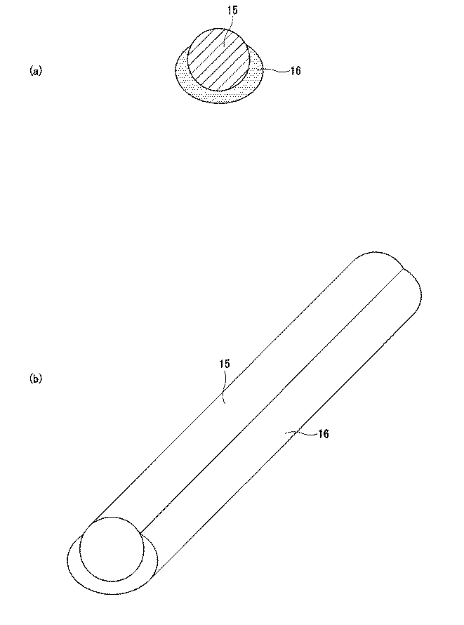
表1に示すように、実施例1〜8では、0.5MPaといった低圧力での押圧にもかかわらず、いずれも接着強度が、0.6〜2.0N/mmとなり、実用に耐えられるものであることがわかる。また、実施例1〜8では、いずれも初期の導通抵抗値が5〜10mΩであり、また、熱衝撃試験後においても8〜13mΩであった。これにより、実施例1〜8では、初期値及び熱衝撃試験後の抵抗値の上昇も殆ど見られず、光電変換効率が低減することがない。一方、比較例1においては、接着強度は1.6N/mmと良好であったが、初期の導通抵抗が50mΩと高く、熱衝撃試験後は導通不良のために抵抗値を検出することができなかった。 As shown in Table 1, in Examples 1-8, despite the pressing at a low pressure of 0.5 MPa, the adhesive strength is 0.6-2.0 N / mm, which can withstand practical use. It can be seen that it is. Moreover, in Examples 1-8, all had an initial conduction resistance value of 5 to 10 mΩ, and 8 to 13 mΩ even after the thermal shock test. Thereby, in Examples 1-8, the raise of the resistance value after an initial value and a thermal shock test is hardly seen, and photoelectric conversion efficiency does not reduce. On the other hand, in Comparative Example 1, the adhesive strength was as good as 1.6 N / mm, but the initial conduction resistance was as high as 50 mΩ, and the resistance value could be detected due to poor conduction after the thermal shock test. There wasn't.
1 太陽電池モジュール、2 太陽電池セル、3 タブ線、4 ストリングス、5 マトリクス、6 シート、7 表面カバー、8 バックシート、9 金属フレーム、10 光電変換素子、11 バスバー電極、12 フィンガー電極、13 裏面電極、14 タブ線接続部、15 線材、16 接着剤層、23 導電性粒子、24 剥離基材、25 リール、30 Ag電極、31 ガラス基板 DESCRIPTION OF SYMBOLS 1 Solar cell module, 2 photovoltaic cell, 3 tab wire, 4 strings, 5 matrix, 6 sheet, 7 surface cover, 8 back sheet, 9 metal frame, 10 photoelectric conversion element, 11 bus bar electrode, 12 finger electrode, 13 back surface Electrode, 14 Tab wire connection part, 15 Wire material, 16 Adhesive layer, 23 Conductive particle, 24 Peeling base material, 25 Reel, 30 Ag electrode, 31 Glass substrate
Claims (14)
上記タブ線は、線状をなし、上記電極との接着部を含む外周面を覆う接着剤層によって上記電極と接着されている太陽電池モジュール。 A plurality of solar cells, and a tab wire that is bonded onto the respective electrodes formed on the surface of the solar cell and the back surface of the adjacent solar cell, and connects the plurality of solar cells,
The said tab wire is a solar cell module which is adhere | attached on the said electrode with the adhesive bond layer which comprises linear form and covers the outer peripheral surface containing the adhesion part with the said electrode.
断面長軸方向の半径をbとし、断面短軸方向の半径をaとしたとき、下記式を満たす請求項1記載の太陽電池モジュール。
0.4≦a≦2 (単位mm)
a≦b≦2 (単位mm) The tab line has a circular cross section or an elliptical shape,
2. The solar cell module according to claim 1, wherein b is a radius in the major axis direction of the cross section and a is a radius in the minor axis direction of the cross section.
0.4 ≦ a ≦ 2 (Unit: mm)
a ≦ b ≦ 2 (unit: mm)
太陽電池セルの表面電極に上記タブ線の一端側を配置し、上記太陽電池セルと隣接する太陽電池セルの裏面電極に上記タブ線の他端側を配置する工程と、
上記タブ線を上記表面電極及び上記裏面電極へ熱加圧し、上記表面電極及び上記裏面電極と上記タブ線との間に流動した接着剤層によって上記タブ線を上記表面電極及び上記裏面電極へ接着する工程とを有する太陽電池モジュールの製造方法。 Using a linear tab line,
Arranging one end side of the tab wire on the surface electrode of the solar battery cell, and arranging the other end side of the tab wire on the back electrode of the solar battery cell adjacent to the solar battery cell;
The tab wire is heat-pressed to the front electrode and the back electrode, and the tab wire is bonded to the front electrode and the back electrode by an adhesive layer that flows between the front electrode and the back electrode and the tab wire. The manufacturing method of the solar cell module which has a process to carry out.
断面長軸方向の半径をbとし、断面短軸方向の半径をaとしたとき、下記式を満たす請求項6〜8のいずれか1項に記載の太陽電池モジュールの製造方法。
0.4≦a≦2 (単位mm)
a≦b≦2 (単位mm) The tab line has a circular cross section or an elliptical shape,
The manufacturing method of the solar cell module of any one of Claims 6-8 which satisfy | fills following formula, when the radius of a cross-sectional major axis direction is set to b and the radius of a cross-sectional minor axis direction is set to a.
0.4 ≦ a ≦ 2 (Unit: mm)
a ≦ b ≦ 2 (unit: mm)
線状をなし、長手方向に亘って少なくとも外周面の50%が接着剤層によって覆われ、上記接着剤層によって上記電極と接着されるタブ線。 In the tab wires that are bonded onto the electrodes formed on the front surface of the solar cell and the back surface of the adjacent solar cell, respectively, and connecting the plurality of solar cells,
A tab wire that is linear and has at least 50% of the outer peripheral surface covered with an adhesive layer in the longitudinal direction and is bonded to the electrode by the adhesive layer.
断面長軸方向の半径をbとし、断面短軸方向の半径をaとしたとき、下記式を満たす請求項11又は請求項12に記載のタブ線。
0.4≦a≦2 (単位mm)
a≦b≦2 (単位mm) It has a circular or oval cross section,
The tab wire according to claim 11 or claim 12, wherein a radius in the major axis direction of the cross section is b and a radius in the minor axis direction of the cross section is a, the following formula is satisfied.
0.4 ≦ a ≦ 2 (Unit: mm)
a ≦ b ≦ 2 (unit: mm)
Priority Applications (3)
| Application Number | Priority Date | Filing Date | Title |
|---|---|---|---|
| JP2011068685A JP5798772B2 (en) | 2011-03-25 | 2011-03-25 | Solar cell module, method for manufacturing solar cell module, tab wire |
| TW101110501A TW201251065A (en) | 2011-03-25 | 2012-03-26 | Solar cell module, method for producing solar cell module, and tab wire |
| PCT/JP2012/057791 WO2012133338A1 (en) | 2011-03-25 | 2012-03-26 | Solar cell module, method for producing solar cell module, and tab wire |
Applications Claiming Priority (1)
| Application Number | Priority Date | Filing Date | Title |
|---|---|---|---|
| JP2011068685A JP5798772B2 (en) | 2011-03-25 | 2011-03-25 | Solar cell module, method for manufacturing solar cell module, tab wire |
Publications (2)
| Publication Number | Publication Date |
|---|---|
| JP2012204666A true JP2012204666A (en) | 2012-10-22 |
| JP5798772B2 JP5798772B2 (en) | 2015-10-21 |
Family
ID=46931055
Family Applications (1)
| Application Number | Title | Priority Date | Filing Date |
|---|---|---|---|
| JP2011068685A Active JP5798772B2 (en) | 2011-03-25 | 2011-03-25 | Solar cell module, method for manufacturing solar cell module, tab wire |
Country Status (3)
| Country | Link |
|---|---|
| JP (1) | JP5798772B2 (en) |
| TW (1) | TW201251065A (en) |
| WO (1) | WO2012133338A1 (en) |
Cited By (6)
| Publication number | Priority date | Publication date | Assignee | Title |
|---|---|---|---|---|
| JP2016012724A (en) * | 2014-06-26 | 2016-01-21 | エルジー エレクトロニクス インコーポレイティド | Solar cell module |
| JP2017034260A (en) * | 2015-08-05 | 2017-02-09 | エルジー エレクトロニクス インコーポレイティド | Ribbon for solar cell panel, method of manufacturing the same, and solar cell panel |
| JP2017228629A (en) * | 2016-06-22 | 2017-12-28 | シャープ株式会社 | Solar battery module |
| JP2019083346A (en) * | 2014-07-07 | 2019-05-30 | エルジー エレクトロニクス インコーポレイティド | Solar cell module and method of manufacturing the same |
| JP2019117860A (en) * | 2017-12-27 | 2019-07-18 | シャープ株式会社 | Double-sided light-receiving solar cell module |
| JP2021168405A (en) * | 2014-09-30 | 2021-10-21 | エルジー エレクトロニクス インコーポレイティドLg Electronics Inc. | Solar cell and solar cell panel including the same |
Families Citing this family (2)
| Publication number | Priority date | Publication date | Assignee | Title |
|---|---|---|---|---|
| US10700223B2 (en) | 2016-12-01 | 2020-06-30 | Shin-Etsu Chemical Co., Ltd. | High photoelectric conversion efficiency solar battery cell and method for manufacturing high photoelectric conversion solar battery cell |
| FR3136589A1 (en) * | 2022-06-14 | 2023-12-15 | Commissariat A L'energie Atomique Et Aux Energies Alternatives | INTERCONNECTION ELEMENT, PHOTOVOLTAIC CHAIN AND ASSOCIATED METHODS |
Citations (5)
| Publication number | Priority date | Publication date | Assignee | Title |
|---|---|---|---|---|
| JPH036867A (en) * | 1989-06-05 | 1991-01-14 | Mitsubishi Electric Corp | Electrode structure of photovoltaic device, forming method, and apparatus for manufacture thereof |
| JPH0918034A (en) * | 1995-06-28 | 1997-01-17 | Canon Inc | Electrode structure of photovoltaic element and its manufacturing method |
| JP2005536894A (en) * | 2002-08-29 | 2005-12-02 | デイ4 エネルギー インコーポレイテッド | Photovoltaic battery electrode, photovoltaic battery and photovoltaic module |
| JP2007103535A (en) * | 2005-09-30 | 2007-04-19 | Sanyo Electric Co Ltd | Solar battery module |
| JP2008263163A (en) * | 2007-03-19 | 2008-10-30 | Sanyo Electric Co Ltd | Solar battery module |
-
2011
- 2011-03-25 JP JP2011068685A patent/JP5798772B2/en active Active
-
2012
- 2012-03-26 WO PCT/JP2012/057791 patent/WO2012133338A1/en active Application Filing
- 2012-03-26 TW TW101110501A patent/TW201251065A/en unknown
Patent Citations (5)
| Publication number | Priority date | Publication date | Assignee | Title |
|---|---|---|---|---|
| JPH036867A (en) * | 1989-06-05 | 1991-01-14 | Mitsubishi Electric Corp | Electrode structure of photovoltaic device, forming method, and apparatus for manufacture thereof |
| JPH0918034A (en) * | 1995-06-28 | 1997-01-17 | Canon Inc | Electrode structure of photovoltaic element and its manufacturing method |
| JP2005536894A (en) * | 2002-08-29 | 2005-12-02 | デイ4 エネルギー インコーポレイテッド | Photovoltaic battery electrode, photovoltaic battery and photovoltaic module |
| JP2007103535A (en) * | 2005-09-30 | 2007-04-19 | Sanyo Electric Co Ltd | Solar battery module |
| JP2008263163A (en) * | 2007-03-19 | 2008-10-30 | Sanyo Electric Co Ltd | Solar battery module |
Cited By (12)
| Publication number | Priority date | Publication date | Assignee | Title |
|---|---|---|---|---|
| JP2016012724A (en) * | 2014-06-26 | 2016-01-21 | エルジー エレクトロニクス インコーポレイティド | Solar cell module |
| US10164130B2 (en) | 2014-06-26 | 2018-12-25 | Lg Electronics Inc. | Solar cell module |
| US10170646B2 (en) | 2014-06-26 | 2019-01-01 | Lg Electronics Inc. | Solar cell module |
| US11201252B2 (en) | 2014-06-26 | 2021-12-14 | Lg Electronics Inc. | Solar cell module |
| US11522092B2 (en) | 2014-06-26 | 2022-12-06 | Shangrao Jinko Solar Technology Development Co., Ltd | Solar cell module |
| JP2019083346A (en) * | 2014-07-07 | 2019-05-30 | エルジー エレクトロニクス インコーポレイティド | Solar cell module and method of manufacturing the same |
| JP2022020793A (en) * | 2014-07-07 | 2022-02-01 | エルジー エレクトロニクス インコーポレイティド | Solar cell module and method of manufacturing the same |
| JP7432571B2 (en) | 2014-07-07 | 2024-02-16 | シャンラオ シンユエン ユエドン テクノロジー デベロップメント シーオー.,エルティーディー | Solar module and its manufacturing method |
| JP2021168405A (en) * | 2014-09-30 | 2021-10-21 | エルジー エレクトロニクス インコーポレイティドLg Electronics Inc. | Solar cell and solar cell panel including the same |
| JP2017034260A (en) * | 2015-08-05 | 2017-02-09 | エルジー エレクトロニクス インコーポレイティド | Ribbon for solar cell panel, method of manufacturing the same, and solar cell panel |
| JP2017228629A (en) * | 2016-06-22 | 2017-12-28 | シャープ株式会社 | Solar battery module |
| JP2019117860A (en) * | 2017-12-27 | 2019-07-18 | シャープ株式会社 | Double-sided light-receiving solar cell module |
Also Published As
| Publication number | Publication date |
|---|---|
| TW201251065A (en) | 2012-12-16 |
| WO2012133338A1 (en) | 2012-10-04 |
| JP5798772B2 (en) | 2015-10-21 |
Similar Documents
| Publication | Publication Date | Title |
|---|---|---|
| JP5798772B2 (en) | Solar cell module, method for manufacturing solar cell module, tab wire | |
| JP5415396B2 (en) | Solar cell module manufacturing method and solar cell module | |
| KR101431404B1 (en) | Solar cell module, manufacturing method for solar cell module, and reel-wound body with tab wire wound therearound | |
| JP5318815B2 (en) | Solar cell module and method for manufacturing solar cell module | |
| JP5676944B2 (en) | Solar cell module and method for manufacturing solar cell module | |
| JP5356347B2 (en) | Solar cell module and method for manufacturing solar cell module | |
| WO2013035667A1 (en) | Solar cell module manufacturing method, solar cell module, and tab wire connection method | |
| JP5892584B2 (en) | Solar cell module and method for manufacturing solar cell module | |
| JP5480120B2 (en) | Solar cell module, solar cell module manufacturing method, solar cell, and tab wire connection method | |
| JP2012124375A (en) | Solar cell module and method for manufacturing the same | |
| JP5828582B2 (en) | Solar cell module, method for manufacturing solar cell module, conductive adhesive | |
| JP5759220B2 (en) | Solar cell module and method for manufacturing solar cell module | |
| WO2013121877A1 (en) | Electrically conductive adhesive agent, solar cell module, and method for producing solar cell module | |
| WO2012099257A1 (en) | Solar cell module and method of manufacturing solar cell module | |
| JP2016021577A (en) | Solar cell module, manufacturing method of solar cell module, conductive adhesive | |
| JP2014107356A (en) | Method of manufacturing solar cell module, and solar cell module | |
| JP2016167641A (en) | Solar battery module and manufacturing method for the same | |
| JP2016001765A (en) | Solar cell module and manufacturing method of the solar cell module |
Legal Events
| Date | Code | Title | Description |
|---|---|---|---|
| A621 | Written request for application examination |
Free format text: JAPANESE INTERMEDIATE CODE: A621 Effective date: 20140206 |
|
| A131 | Notification of reasons for refusal |
Free format text: JAPANESE INTERMEDIATE CODE: A131 Effective date: 20150106 |
|
| A521 | Request for written amendment filed |
Free format text: JAPANESE INTERMEDIATE CODE: A523 Effective date: 20150226 |
|
| TRDD | Decision of grant or rejection written | ||
| A01 | Written decision to grant a patent or to grant a registration (utility model) |
Free format text: JAPANESE INTERMEDIATE CODE: A01 Effective date: 20150804 |
|
| A61 | First payment of annual fees (during grant procedure) |
Free format text: JAPANESE INTERMEDIATE CODE: A61 Effective date: 20150824 |
|
| R150 | Certificate of patent or registration of utility model |
Ref document number: 5798772 Country of ref document: JP Free format text: JAPANESE INTERMEDIATE CODE: R150 |
|
| R250 | Receipt of annual fees |
Free format text: JAPANESE INTERMEDIATE CODE: R250 |
|
| R250 | Receipt of annual fees |
Free format text: JAPANESE INTERMEDIATE CODE: R250 |
|
| R250 | Receipt of annual fees |
Free format text: JAPANESE INTERMEDIATE CODE: R250 |
|
| R250 | Receipt of annual fees |
Free format text: JAPANESE INTERMEDIATE CODE: R250 |
|
| R250 | Receipt of annual fees |
Free format text: JAPANESE INTERMEDIATE CODE: R250 |
|
| R250 | Receipt of annual fees |
Free format text: JAPANESE INTERMEDIATE CODE: R250 |