JP2011512037A - System and method for emitter layer shaping - Google Patents
System and method for emitter layer shaping Download PDFInfo
- Publication number
- JP2011512037A JP2011512037A JP2010546060A JP2010546060A JP2011512037A JP 2011512037 A JP2011512037 A JP 2011512037A JP 2010546060 A JP2010546060 A JP 2010546060A JP 2010546060 A JP2010546060 A JP 2010546060A JP 2011512037 A JP2011512037 A JP 2011512037A
- Authority
- JP
- Japan
- Prior art keywords
- emitter
- led
- geometric configuration
- area
- substrate
- Prior art date
- Legal status (The legal status is an assumption and is not a legal conclusion. Google has not performed a legal analysis and makes no representation as to the accuracy of the status listed.)
- Withdrawn
Links
- 238000000034 method Methods 0.000 title claims abstract description 88
- 238000007493 shaping process Methods 0.000 title abstract description 22
- 239000000758 substrate Substances 0.000 claims abstract description 153
- 238000005530 etching Methods 0.000 claims abstract description 46
- 239000000463 material Substances 0.000 claims description 136
- JMASRVWKEDWRBT-UHFFFAOYSA-N Gallium nitride Chemical compound [Ga]#N JMASRVWKEDWRBT-UHFFFAOYSA-N 0.000 claims description 62
- 230000005855 radiation Effects 0.000 claims description 49
- 230000000670 limiting effect Effects 0.000 claims description 24
- 238000000605 extraction Methods 0.000 claims description 18
- HBMJWWWQQXIZIP-UHFFFAOYSA-N silicon carbide Chemical compound [Si+]#[C-] HBMJWWWQQXIZIP-UHFFFAOYSA-N 0.000 claims description 11
- 238000000059 patterning Methods 0.000 claims description 7
- 230000005540 biological transmission Effects 0.000 claims description 6
- 239000006117 anti-reflective coating Substances 0.000 claims description 4
- 230000008021 deposition Effects 0.000 claims description 4
- 239000000126 substance Substances 0.000 claims description 3
- 229910018072 Al 2 O 3 Inorganic materials 0.000 claims 3
- TWNQGVIAIRXVLR-UHFFFAOYSA-N oxo(oxoalumanyloxy)alumane Chemical compound O=[Al]O[Al]=O TWNQGVIAIRXVLR-UHFFFAOYSA-N 0.000 claims 3
- 238000009826 distribution Methods 0.000 abstract description 18
- 239000010410 layer Substances 0.000 description 171
- 229910002601 GaN Inorganic materials 0.000 description 59
- 229910052594 sapphire Inorganic materials 0.000 description 34
- 239000010980 sapphire Substances 0.000 description 34
- 230000008569 process Effects 0.000 description 28
- 239000007787 solid Substances 0.000 description 18
- 230000008901 benefit Effects 0.000 description 16
- 238000004519 manufacturing process Methods 0.000 description 15
- 239000002245 particle Substances 0.000 description 15
- 239000011248 coating agent Substances 0.000 description 13
- 238000000576 coating method Methods 0.000 description 13
- 239000000460 chlorine Substances 0.000 description 12
- 229920002120 photoresistant polymer Polymers 0.000 description 12
- 238000000465 moulding Methods 0.000 description 11
- XLYOFNOQVPJJNP-UHFFFAOYSA-N water Substances O XLYOFNOQVPJJNP-UHFFFAOYSA-N 0.000 description 11
- 238000000151 deposition Methods 0.000 description 10
- 229910052751 metal Inorganic materials 0.000 description 10
- 239000002184 metal Substances 0.000 description 10
- OAICVXFJPJFONN-UHFFFAOYSA-N Phosphorus Chemical compound [P] OAICVXFJPJFONN-UHFFFAOYSA-N 0.000 description 9
- 230000002829 reductive effect Effects 0.000 description 9
- 229910010271 silicon carbide Inorganic materials 0.000 description 8
- 230000007704 transition Effects 0.000 description 7
- 238000009792 diffusion process Methods 0.000 description 6
- 230000003287 optical effect Effects 0.000 description 6
- 239000004065 semiconductor Substances 0.000 description 6
- 230000008859 change Effects 0.000 description 5
- 238000005520 cutting process Methods 0.000 description 5
- 238000005286 illumination Methods 0.000 description 5
- 238000009616 inductively coupled plasma Methods 0.000 description 5
- 230000007480 spreading Effects 0.000 description 5
- 238000003892 spreading Methods 0.000 description 5
- 238000010521 absorption reaction Methods 0.000 description 4
- 150000001875 compounds Chemical class 0.000 description 4
- 238000011161 development Methods 0.000 description 4
- 230000018109 developmental process Effects 0.000 description 4
- 238000001312 dry etching Methods 0.000 description 4
- 238000005516 engineering process Methods 0.000 description 4
- 230000004907 flux Effects 0.000 description 4
- 239000007789 gas Substances 0.000 description 4
- KRHYYFGTRYWZRS-UHFFFAOYSA-N hydrofluoric acid Substances F KRHYYFGTRYWZRS-UHFFFAOYSA-N 0.000 description 4
- 238000000608 laser ablation Methods 0.000 description 4
- 210000002381 plasma Anatomy 0.000 description 4
- 238000001020 plasma etching Methods 0.000 description 4
- 238000002679 ablation Methods 0.000 description 3
- 238000007792 addition Methods 0.000 description 3
- 230000015572 biosynthetic process Effects 0.000 description 3
- 239000002775 capsule Substances 0.000 description 3
- 239000013078 crystal Substances 0.000 description 3
- 238000013461 design Methods 0.000 description 3
- 238000010586 diagram Methods 0.000 description 3
- 239000010432 diamond Substances 0.000 description 3
- 229910003460 diamond Inorganic materials 0.000 description 3
- 239000011521 glass Substances 0.000 description 3
- 238000000227 grinding Methods 0.000 description 3
- 230000006872 improvement Effects 0.000 description 3
- 239000000203 mixture Substances 0.000 description 3
- 238000012986 modification Methods 0.000 description 3
- 230000004048 modification Effects 0.000 description 3
- 239000002105 nanoparticle Substances 0.000 description 3
- 230000009471 action Effects 0.000 description 2
- 238000004458 analytical method Methods 0.000 description 2
- 238000013459 approach Methods 0.000 description 2
- 210000004027 cell Anatomy 0.000 description 2
- 238000006243 chemical reaction Methods 0.000 description 2
- 238000004590 computer program Methods 0.000 description 2
- 230000000694 effects Effects 0.000 description 2
- 230000005670 electromagnetic radiation Effects 0.000 description 2
- 238000000407 epitaxy Methods 0.000 description 2
- 230000006870 function Effects 0.000 description 2
- 230000017525 heat dissipation Effects 0.000 description 2
- 238000001465 metallisation Methods 0.000 description 2
- QPJSUIGXIBEQAC-UHFFFAOYSA-N n-(2,4-dichloro-5-propan-2-yloxyphenyl)acetamide Chemical compound CC(C)OC1=CC(NC(C)=O)=C(Cl)C=C1Cl QPJSUIGXIBEQAC-UHFFFAOYSA-N 0.000 description 2
- 238000005498 polishing Methods 0.000 description 2
- 238000004321 preservation Methods 0.000 description 2
- 238000012545 processing Methods 0.000 description 2
- 230000001902 propagating effect Effects 0.000 description 2
- 230000003746 surface roughness Effects 0.000 description 2
- 238000001039 wet etching Methods 0.000 description 2
- DDFHBQSCUXNBSA-UHFFFAOYSA-N 5-(5-carboxythiophen-2-yl)thiophene-2-carboxylic acid Chemical compound S1C(C(=O)O)=CC=C1C1=CC=C(C(O)=O)S1 DDFHBQSCUXNBSA-UHFFFAOYSA-N 0.000 description 1
- ZCYVEMRRCGMTRW-UHFFFAOYSA-N 7553-56-2 Chemical compound [I] ZCYVEMRRCGMTRW-UHFFFAOYSA-N 0.000 description 1
- 229910002704 AlGaN Inorganic materials 0.000 description 1
- ZAMOUSCENKQFHK-UHFFFAOYSA-N Chlorine atom Chemical compound [Cl] ZAMOUSCENKQFHK-UHFFFAOYSA-N 0.000 description 1
- 229910018503 SF6 Inorganic materials 0.000 description 1
- 229910004298 SiO 2 Inorganic materials 0.000 description 1
- VYPSYNLAJGMNEJ-UHFFFAOYSA-N Silicium dioxide Chemical compound O=[Si]=O VYPSYNLAJGMNEJ-UHFFFAOYSA-N 0.000 description 1
- 239000003082 abrasive agent Substances 0.000 description 1
- 230000006978 adaptation Effects 0.000 description 1
- 238000004364 calculation method Methods 0.000 description 1
- 238000001311 chemical methods and process Methods 0.000 description 1
- 238000005229 chemical vapour deposition Methods 0.000 description 1
- 229910052801 chlorine Inorganic materials 0.000 description 1
- 239000003086 colorant Substances 0.000 description 1
- 230000000295 complement effect Effects 0.000 description 1
- 238000005094 computer simulation Methods 0.000 description 1
- 239000004020 conductor Substances 0.000 description 1
- 238000010276 construction Methods 0.000 description 1
- 230000001419 dependent effect Effects 0.000 description 1
- 238000001514 detection method Methods 0.000 description 1
- 238000005553 drilling Methods 0.000 description 1
- 238000004836 empirical method Methods 0.000 description 1
- 239000008393 encapsulating agent Substances 0.000 description 1
- 238000004134 energy conservation Methods 0.000 description 1
- 229910052736 halogen Inorganic materials 0.000 description 1
- 150000002367 halogens Chemical class 0.000 description 1
- 238000002248 hydride vapour-phase epitaxy Methods 0.000 description 1
- 150000004678 hydrides Chemical class 0.000 description 1
- 230000003993 interaction Effects 0.000 description 1
- 230000002452 interceptive effect Effects 0.000 description 1
- 229910052740 iodine Inorganic materials 0.000 description 1
- 239000011630 iodine Substances 0.000 description 1
- 150000002500 ions Chemical class 0.000 description 1
- 239000007788 liquid Substances 0.000 description 1
- 239000004973 liquid crystal related substance Substances 0.000 description 1
- 239000007791 liquid phase Substances 0.000 description 1
- 230000000873 masking effect Effects 0.000 description 1
- 229910001092 metal group alloy Inorganic materials 0.000 description 1
- 238000003801 milling Methods 0.000 description 1
- 229910003465 moissanite Inorganic materials 0.000 description 1
- 238000001451 molecular beam epitaxy Methods 0.000 description 1
- 239000003921 oil Substances 0.000 description 1
- 238000005457 optimization Methods 0.000 description 1
- 238000002161 passivation Methods 0.000 description 1
- 239000012071 phase Substances 0.000 description 1
- 238000001259 photo etching Methods 0.000 description 1
- 239000004033 plastic Substances 0.000 description 1
- 229920000642 polymer Polymers 0.000 description 1
- 239000011241 protective layer Substances 0.000 description 1
- 230000008707 rearrangement Effects 0.000 description 1
- 238000000926 separation method Methods 0.000 description 1
- 229910052814 silicon oxide Inorganic materials 0.000 description 1
- 238000004088 simulation Methods 0.000 description 1
- 238000001228 spectrum Methods 0.000 description 1
- 239000007858 starting material Substances 0.000 description 1
- 238000006467 substitution reaction Methods 0.000 description 1
- SFZCNBIFKDRMGX-UHFFFAOYSA-N sulfur hexafluoride Chemical group FS(F)(F)(F)(F)F SFZCNBIFKDRMGX-UHFFFAOYSA-N 0.000 description 1
- 229960000909 sulfur hexafluoride Drugs 0.000 description 1
- FAQYAMRNWDIXMY-UHFFFAOYSA-N trichloroborane Chemical compound ClB(Cl)Cl FAQYAMRNWDIXMY-UHFFFAOYSA-N 0.000 description 1
- 238000009827 uniform distribution Methods 0.000 description 1
- 238000007740 vapor deposition Methods 0.000 description 1
- 239000012808 vapor phase Substances 0.000 description 1
- 239000002699 waste material Substances 0.000 description 1
Images


Classifications
-
- H—ELECTRICITY
- H01—ELECTRIC ELEMENTS
- H01L—SEMICONDUCTOR DEVICES NOT COVERED BY CLASS H10
- H01L33/00—Semiconductor devices having potential barriers specially adapted for light emission; Processes or apparatus specially adapted for the manufacture or treatment thereof or of parts thereof; Details thereof
- H01L33/02—Semiconductor devices having potential barriers specially adapted for light emission; Processes or apparatus specially adapted for the manufacture or treatment thereof or of parts thereof; Details thereof characterised by the semiconductor bodies
- H01L33/20—Semiconductor devices having potential barriers specially adapted for light emission; Processes or apparatus specially adapted for the manufacture or treatment thereof or of parts thereof; Details thereof characterised by the semiconductor bodies with a particular shape, e.g. curved or truncated substrate
-
- H—ELECTRICITY
- H01—ELECTRIC ELEMENTS
- H01L—SEMICONDUCTOR DEVICES NOT COVERED BY CLASS H10
- H01L33/00—Semiconductor devices having potential barriers specially adapted for light emission; Processes or apparatus specially adapted for the manufacture or treatment thereof or of parts thereof; Details thereof
- H01L33/02—Semiconductor devices having potential barriers specially adapted for light emission; Processes or apparatus specially adapted for the manufacture or treatment thereof or of parts thereof; Details thereof characterised by the semiconductor bodies
- H01L33/08—Semiconductor devices having potential barriers specially adapted for light emission; Processes or apparatus specially adapted for the manufacture or treatment thereof or of parts thereof; Details thereof characterised by the semiconductor bodies with a plurality of light emitting regions, e.g. laterally discontinuous light emitting layer or photoluminescent region integrated within the semiconductor body
-
- H—ELECTRICITY
- H01—ELECTRIC ELEMENTS
- H01L—SEMICONDUCTOR DEVICES NOT COVERED BY CLASS H10
- H01L33/00—Semiconductor devices having potential barriers specially adapted for light emission; Processes or apparatus specially adapted for the manufacture or treatment thereof or of parts thereof; Details thereof
- H01L33/02—Semiconductor devices having potential barriers specially adapted for light emission; Processes or apparatus specially adapted for the manufacture or treatment thereof or of parts thereof; Details thereof characterised by the semiconductor bodies
- H01L33/26—Materials of the light emitting region
- H01L33/30—Materials of the light emitting region containing only elements of Group III and Group V of the Periodic Table
- H01L33/32—Materials of the light emitting region containing only elements of Group III and Group V of the Periodic Table containing nitrogen
Landscapes
- Engineering & Computer Science (AREA)
- Manufacturing & Machinery (AREA)
- Computer Hardware Design (AREA)
- Microelectronics & Electronic Packaging (AREA)
- Power Engineering (AREA)
- Led Devices (AREA)
Abstract
開示されるLEDの実施形態は、LEDの光出力を最大化し、所望の強度分布を達成するように、LEDの基板に対して制御された深さまたは高さに成形される、エミッタ層を有する。いくつかの実施形態において、LEDの放出面は、放射輝度を保存するように選択されてもよい。いくつかの実施形態において、基板および側壁を含むLED全体の成形、または基板のみの成形は、エミッタ層で生成される光の100%または約100%をエミッタ層から抽出することができる。いくつかの実施形態において、全効率は、少なくとも90%以上である。いくつかの実施形態において、エミッタ層は、エッチング、機械的成形、または種々の成形方法の組み合せにより、成形することができる。いくつかの実施形態において、微小なエミッタを形成するように、エミッタ層の一部のみが成形される。非成形部分は、LEDの連続的な電気接続を形成する。The disclosed LED embodiments have an emitter layer that is shaped to a controlled depth or height relative to the substrate of the LED to maximize the light output of the LED and achieve a desired intensity distribution. . In some embodiments, the emitting surface of the LED may be selected to preserve radiance. In some embodiments, shaping the entire LED, including the substrate and sidewalls, or shaping only the substrate can extract 100% or about 100% of the light generated in the emitter layer from the emitter layer. In some embodiments, the overall efficiency is at least 90% or higher. In some embodiments, the emitter layer can be formed by etching, mechanical forming, or a combination of various forming methods. In some embodiments, only a portion of the emitter layer is shaped to form a tiny emitter. The non-molded part forms a continuous electrical connection for the LED.
Description
(関連出願の相互参照)
本出願は、米国特許法第119条(e)項の下、2008年2月8日に出願された「EMITTER LAYER SHAPING」というタイトルの米国仮特許出願第61/027,354号および2008年11月25日に出願された「EMITTER LAYER SHAPING」というタイトルの米国仮特許出願第61/049,964号の優先権の利益を主張する。本出願は、2007年10月1日に出願された「LED SYSTEM AND METHOD」というタイトルの米国特許出願第11/906,219号および2007年10月1日に出願された「LED SYSTEM AND METHOD」というタイトルの米国特許出願第11/906,194号に関連しており、その両方が2006年10月2日に出願された「SHAPED LIGHT EMITTING DIODES」というタイトルの米国仮特許出願第60/827,818号および2007年1月22日に出願された「SYSTEM AND METHOD FOR A SHAPED SUBSTRATE LED」というタイトルの米国仮特許出願第60/881,785号の優先権を主張する。すべての出願が本明細書に参考として十分に援用される。
(Cross-reference of related applications)
This application is filed under US Patent Act No. 119 (e), US Provisional Patent Application Nos. 61 / 027,354 and 11/2008, filed February 8, 2008, entitled “EMITTER LAYER SHAPING”. Claims the benefit of priority of US Provisional Patent Application No. 61 / 049,964, filed May 25, entitled “EMITTER LAYER SHAPING”. This application is based on US patent application Ser. No. 11 / 906,219 entitled “LED SYSTEM AND METHOD” filed Oct. 1, 2007 and “LED SYSTEM AND METHOD” filed Oct. 1, 2007. No. 11 / 906,194, entitled US Provisional Patent Application No. 60/827, entitled “SHAPED LIGHT MITTING DIODES,” filed October 2, 2006, both. No. 818 and US Provisional Patent Application No. 60 / 881,785 entitled “SYSTEM AND METHOD FOR A SHAPED SUBSTRATE LED” filed Jan. 22, 2007. All applications are fully incorporated herein by reference.
(本開示の分野)
本開示は、概して、発光ダイオード(LED)デバイスに関し、より具体的には、任意のLEDの光抽出効率を最大化するようなエミッタ材料の成形のためのシステムおよび方法に関する。
(Field of this disclosure)
The present disclosure relates generally to light emitting diode (LED) devices, and more specifically to systems and methods for shaping emitter materials to maximize the light extraction efficiency of any LED.
(背景)
発光ダイオード(「LED」)は、電子機器のいたるところに見られる。それらは、デジタル表示、照明システム、コンピュータ、テレビ、携帯電話、およびその他の様々なデバイスにおいて使用されている。LED技術の発展により、1つ以上のLEDを使用した白色光の生成のための方法およびシステムがもたらされた。LED技術の発展により、従来よりも多くの光子、ひいてはより多くの光を生成するLEDがもたらされた。これら2つの技術的発展の最たるものは、コンピュータにおいて真空管がトランジスタに置き換わったのと同じように、LEDが多くの従来型光源、例えば白熱電球、蛍光灯、ハロゲン球等を補完する、あるいは置き換えるように使用されていることである。
(background)
Light emitting diodes (“LEDs”) are found throughout electronic equipment. They are used in digital displays, lighting systems, computers, televisions, cell phones, and various other devices. Advances in LED technology have provided methods and systems for the generation of white light using one or more LEDs. The development of LED technology has led to LEDs that produce more photons and thus more light than before. The best of these two technological developments is that LEDs complement or replace many conventional light sources, such as incandescent bulbs, fluorescent lamps, halogen bulbs, etc., just as a vacuum tube is replaced by a transistor in a computer. It is used for.
LEDは、赤色、緑色、および青色を含む多くの色で生成される。白色光を生成する1つの方法は、互いに組み合わされた赤色、緑色および青色LEDが関与する。赤色、緑色、および青色(RGB)LEDの組み合わせで形成される光源は、人間の目により白色光として認識されるものを生成する。これは、人間の目が3種類の色受容体を有し、各種類は青色、緑色または赤色に対し感受性であるために生じる。 LEDs are produced in many colors including red, green, and blue. One method of producing white light involves red, green and blue LEDs combined with each other. A light source formed by a combination of red, green, and blue (RGB) LEDs produces what is recognized as white light by the human eye. This occurs because the human eye has three types of color receptors, each type being sensitive to blue, green or red.
LED源から白色光を生成する第2の方法は、単一色(例:青色)の短波長LEDから光を形成し、その光の一部をリン光体または同様の光子変換材料に衝突させることである。リン光体はより高いエネルギーの短波長光波を吸収し、より低い長波長光を再放射する。例えば、黄色領域(緑色と赤色の間)の光を放出するリン光体が選択された場合、人間の目はそのような光を白色光として認識する。これは、黄色光が、目の赤色および緑色受容体の両方を刺激するために生じる。ナノ粒子または他の同様の光ルミネセンス材料等のその他の材料を使用して、ほぼ同じ方式で白色光を生成することができる。 A second method of generating white light from an LED source is to form light from a single color (eg, blue) short wavelength LED and strike a portion of that light against a phosphor or similar photon conversion material. It is. The phosphor absorbs higher energy short wavelength light waves and re-emits lower long wavelength light. For example, if a phosphor that emits light in the yellow region (between green and red) is selected, the human eye will recognize such light as white light. This occurs because yellow light stimulates both the red and green receptors of the eye. Other materials such as nanoparticles or other similar photoluminescent materials can be used to produce white light in much the same manner.
また、白色光は、紫外(UV)LEDおよび3つの別個のRGBリン光体を使用して生成することもできる。さらに、白色光は、青色LEDおよび黄色LEDから生成することができ、また青色、緑色、黄色、および赤色LEDを組み合わせて使用して生成することもできる。 White light can also be generated using an ultraviolet (UV) LED and three separate RGB phosphors. Further, white light can be generated from blue and yellow LEDs, and can also be generated using a combination of blue, green, yellow, and red LEDs.
LED構築のための現在の工業的手法は、GaNまたはInGaN等の層が堆積される基板(通常は単結晶サファイアまたは炭化ケイ素)を使用することである。1つ以上の層(例:GaNまたはInGaN)が光子生成および電流伝導を可能とし得る。通常は、窒化ガリウム(GaN)の第1の層が基板の表面上に施され、基板の結晶構造から、光子生成または電流伝導を可能とするドープされた層の結晶構造への遷移領域を形成する。この後、通常はGaNのnドープ層が形成される。次の層は、光子を生成し、また所望の光の波長を生成するために必要な材料でドープされた、InGaN、AlGaN、AlInGaNまたはその他の化合物の半導体材料層であってもよい。次の層は、通常はGaNのPドープ層である。この構造は、エッチングおよび堆積によりさらに改質され、デバイスへの電気接続のための金属部位を形成する。 The current industrial approach for LED construction is to use a substrate (usually single crystal sapphire or silicon carbide) on which a layer such as GaN or InGaN is deposited. One or more layers (eg, GaN or InGaN) may allow photon generation and current conduction. Typically, a first layer of gallium nitride (GaN) is applied on the surface of the substrate to form a transition region from the crystal structure of the substrate to the crystal structure of the doped layer that allows photon generation or current conduction To do. Thereafter, an n-doped layer of GaN is usually formed. The next layer may be a semiconductor material layer of InGaN, AlGaN, AlInGaN or other compound doped with the materials necessary to generate photons and to generate the desired wavelength of light. The next layer is usually a P-doped layer of GaN. This structure is further modified by etching and deposition to form metal sites for electrical connection to the device.
従来型のダイオードの場合のように、LEDの動作中、余剰電子がn型半導体からp型半導体の正孔に移動する。LEDにおいて、光子は化合物半導体層に放出され、このプロセスの間に光を生成する。 As in the case of a conventional diode, during the operation of the LED, surplus electrons move from the n-type semiconductor to the holes of the p-type semiconductor. In an LED, photons are emitted into the compound semiconductor layer, producing light during this process.
通常の製造プロセスにおいて、基板は、ウエハ形態で製造され、層がウエハの表面に施される。層がドープまたはエッチングされ、上述の様々なプロセスを使用してすべての特徴が画定されると、個々のLEDはウエハから分離される。通常は、LEDは直立した側面を有する正方形または長方形である。これは著しい効率損失をもたらす可能性があり、また放出された光の放出パターンを低下させる可能性がある。より望ましい出力を達成するために、プラスチックドーム等の別個の光学デバイスがLEDの上に設置されることが多い。 In a normal manufacturing process, the substrate is manufactured in wafer form and a layer is applied to the surface of the wafer. Once the layers are doped or etched and all features are defined using the various processes described above, the individual LEDs are separated from the wafer. Typically, LEDs are square or rectangular with upright sides. This can result in significant efficiency losses and can reduce the emission pattern of the emitted light. In order to achieve a more desirable output, a separate optical device such as a plastic dome is often placed on top of the LED.
多くのLED用途において、多くの場合白色光のワットあたりのルーメン(lm/W)、または青色等のより短波長光のワットあたりのミリワット(mW/W)で表現される量である、所与の電力入力に対する可視光出力を最大化することが望ましい。既存のLED技術は、通常は「全体的効率」または「ウォールプラグ効率」と呼ばれるこの比率を増加させるように試みている場合がある。しかしながら、既存のLED技術では、まだ低い全体的効率および低い抽出効率が問題となっている。 For many LED applications, a quantity often expressed in lumens per watt of white light (lm / W) or milliwatts per watt of shorter wavelength light such as blue (mW / W) It is desirable to maximize the visible light output for any power input. Existing LED technology may attempt to increase this ratio, commonly referred to as “overall efficiency” or “wall plug efficiency”. However, with existing LED technology, low overall efficiency and low extraction efficiency are still problematic.
(概要)
本明細書で開示された完全エミッタ層成形(Complete Emitter Layer Shaping、CELS)プロセスの実施形態は、そのエミッタ材料の成形により、任意の発光ダイオードの光抽出効率の最大化における幾何学的および光学的解決策を提供し得る。いくつかの実施形態において、このプロセスはGaN成形と呼ばれる。
(Overview)
Embodiments of the Complete Emitter Layer Shaping (CELS) process disclosed herein are geometric and optical in maximizing the light extraction efficiency of any light emitting diode by shaping the emitter material. A solution can be provided. In some embodiments, this process is referred to as GaN shaping.
本明細書で開示された実施形態は、一般に、紫外、可視および赤外光を含むに光に関連した電磁スペクトルに関して記述される。本明細書に開示された原理は、使用される好適な材料が対象となる波長を透過する、任意の波長の電磁放射線に適用することができる。当業者に理解されるように、本明細書に開示されたエミッタ層成形方法およびシステムは、広範な波長に適合するように同様に実装され得る。対象となる波長領域の例は、テラヘルツ周波数範囲である。 The embodiments disclosed herein are generally described in terms of the electromagnetic spectrum associated with light, including ultraviolet, visible and infrared light. The principles disclosed herein can be applied to electromagnetic radiation of any wavelength where the preferred material used is transparent to the wavelength of interest. As will be appreciated by those skilled in the art, the emitter layer shaping methods and systems disclosed herein can be similarly implemented to accommodate a wide range of wavelengths. An example of a wavelength region of interest is the terahertz frequency range.
LEDの放射材料は、いくつかの基板上で成長され得る。現在では、InGaN LEDの大多数はサファイア基板上に成長される。サファイアの屈折率は放射材料(InGaN)よりも極めて低く、したがってサファイア基板に入る光子の数は大きく低減される。放射材料の成形において、GaN材料から放出された光は、サファイア基板中に逃げ、最終的には空気中に逃げることができる。 The emissive material of the LED can be grown on several substrates. Currently, the majority of InGaN LEDs are grown on sapphire substrates. The refractive index of sapphire is much lower than that of the emissive material (InGaN), so the number of photons entering the sapphire substrate is greatly reduced. In the formation of the radiating material, the light emitted from the GaN material can escape into the sapphire substrate and eventually escape into the air.
今日市場に出回っている青色および緑色LEDのほぼすべては、サファイアまたは炭化ケイ素基板に施された第1の層の材料としてGaN(窒化ガリウム)を使用して構築されている。また、施される実際の層は多様で複雑であり、GaNだけでなく、InGaN、AlInGaP等の化合物半導体材料も含む。今日の科学における最近の発展は、LED層において、GaNだけでなくその他の材料を使用することを含む。本出願に記載された技術は、発光デバイスにおけるすべてのあらゆるそのような層に適用される。本明細書で使用される場合、「完全エミッタ層成形」および「CELS」および「GaN成形」という語句は、実際にはGaN、ある他の材料、またはそれらの組み合わせを成形するか否かによらず、すべてのそのような行為を含むように意図される。計算および例示を目的として、本出願全体にわたりGaNが放射材料として使用される。しかしながら、方程式および説明は、他の材料の組全体に等しく適用され、本明細書に開示された例により限定されないことが、当業者に理解される。 Nearly all of the blue and green LEDs on the market today are constructed using GaN (gallium nitride) as the first layer material applied to a sapphire or silicon carbide substrate. Moreover, the actual layers applied are diverse and complex, and include not only GaN but also compound semiconductor materials such as InGaN and AlInGaP. Recent developments in today's science include the use of other materials in addition to GaN in LED layers. The techniques described in this application apply to all such layers in light emitting devices. As used herein, the terms “full emitter layer shaping” and “CELS” and “GaN shaping” depend on whether actually shaping GaN, some other material, or a combination thereof. Rather, it is intended to include all such actions. For purposes of calculation and illustration, GaN is used as the emissive material throughout the application. However, it will be appreciated by those skilled in the art that the equations and descriptions apply equally to other entire sets of materials and are not limited by the examples disclosed herein.
従来のLEDは、高い屈折率に起因して、光エネルギーが生成される光抽出効率が低いことが問題となっている。高い屈折率の材料からより低い屈折率の材料への移行において、全反射(TIR)は光のエスケープコーンを制限する。エスケープコーン角度は臨界角である。この臨界角は、スネルの法則を用いて計算することができる。 Conventional LEDs have a problem in that light extraction efficiency for generating light energy is low due to a high refractive index. In the transition from a high index material to a lower index material, total internal reflection (TIR) limits the light escape cone. The escape cone angle is a critical angle. This critical angle can be calculated using Snell's law.
一実施形態において、LEDのエミッタ層の一部は、LEDの基板に対して制御された深さまたは高さに成形される。本明細書に開示された実施形態において、エミッタ層は、マイクロLEDとも呼ばれる小型エミッタの配列を備える。いくつかの実施形態において、マイクロLEDの各々は、正方形、長方形または六角形の形状を有する。いくつかの実施形態において、エミッタ層は、エッチングにより成形される。一実施形態において、基板はサファイアである。一実施形態において、エミッタ層材料は、基板と連続的に接触している。一実施形態において、エミッタ層材料は、基板と電気的に接触している。一実施形態において、エミッタ層材料は、基板と電気面または連続的な電気接続を形成する。 In one embodiment, a portion of the LED emitter layer is shaped to a controlled depth or height relative to the LED substrate. In the embodiments disclosed herein, the emitter layer comprises an array of small emitters, also called micro LEDs. In some embodiments, each of the micro LEDs has a square, rectangular or hexagonal shape. In some embodiments, the emitter layer is shaped by etching. In one embodiment, the substrate is sapphire. In one embodiment, the emitter layer material is in continuous contact with the substrate. In one embodiment, the emitter layer material is in electrical contact with the substrate. In one embodiment, the emitter layer material forms an electrical surface or continuous electrical connection with the substrate.
いくつかの実施形態において、エミッタ層の一部のみが成形される。いくつかの実施形態において、LEDのエミッタ層は、成形部分および非成形部分または領域を備える。いくつかの実施形態において、エミッタ層の形成部分は、制御された深さまたは高さを有し、エミッタ層の非成形部分または領域は、電気面またはほぼ連続的な電気接続を形成し、概して基盤と連続的に接触している。いくつかの実施形態において、エミッタ層の非成形部分は、端部において電源と結合されてもよい。いくつかの実施形態において、エミッタ層の1つ以上の成形部分は、電源と結合されてもよい。 In some embodiments, only a portion of the emitter layer is shaped. In some embodiments, the emitter layer of the LED comprises a shaped portion and a non-shaped portion or region. In some embodiments, the formed portion of the emitter layer has a controlled depth or height, and the unshaped portion or region of the emitter layer forms an electrical surface or a substantially continuous electrical connection, generally In continuous contact with the base. In some embodiments, the unshaped portion of the emitter layer may be coupled to a power source at the ends. In some embodiments, one or more shaped portions of the emitter layer may be coupled to a power source.
一実施形態において、制限放射線は、エミッタ層の成形部分おける最長距離または近似最長距離を横断し得る。いくつかの実施形態において、制限放射線は、基板に対するエミッタ層の成形分の深さまたは高さで概して終端するように選択され得る。いくつかの実施形態において、エミッタ層材料は、エミッタ層の成形部分における最長距離または近似最長距離を横断する1つ以上の制限放射線に基づき成形され得る。 In one embodiment, the limiting radiation may traverse the longest or approximate longest distance in the shaped portion of the emitter layer. In some embodiments, the limiting radiation can be selected to generally terminate at a shaped depth or height of the emitter layer relative to the substrate. In some embodiments, the emitter layer material may be shaped based on one or more limiting radiations that traverse the longest or approximate longest distance in the shaped portion of the emitter layer.
いくつかの実施形態において、LEDの側壁はまた、全反射を用いてLEDの光出力を最大化し、所望の強度分布を達成するように成形され得る。いくつかの実施形態において、LEDの放出面は、放射輝度を保存するように選択され得る。 In some embodiments, the sidewalls of the LED can also be shaped to use total internal reflection to maximize the light output of the LED and achieve a desired intensity distribution. In some embodiments, the emission surface of the LED can be selected to preserve radiance.
いくつかの実施形態において、LEDの側壁形状は、以下の制約に基づいて経験的に決定される。
・側壁に衝突するエミッタから発するすべての放射線は、臨界角以上の角度で側壁に衝突すべきである。
・側壁で反射するすべての放射線は、出口表面に向かって反射すべきであり、出口表面における入射角は臨界角未満である必要がある。
In some embodiments, the LED sidewall shape is determined empirically based on the following constraints.
• All radiation emanating from the emitter impinging on the sidewall should impinge on the sidewall at an angle above the critical angle.
-All radiation reflected at the sidewall should be reflected towards the exit surface and the angle of incidence at the exit surface should be less than the critical angle.
いくつかの実施形態において、側壁の形状の基準は、放出面における光の強度の均一性もしくは無限大でのガウス分布、または両方、またはその他の組の条件をさらに含み得る。このように、側壁は、放出された光が所望の強度または角度で基板に誘導されるのを確実とするように成形され得る。いくつかの実施形態において、所望の強度または角度は、基板の特性、例えば基板、エミッタ材料または他の材料の屈折率等に基づいて決定され得る。 In some embodiments, the sidewall shape criteria may further include uniformity of light intensity at the emission surface or a Gaussian distribution at infinity, or both, or other sets of conditions. In this way, the sidewalls can be shaped to ensure that the emitted light is directed to the substrate at the desired intensity or angle. In some embodiments, the desired intensity or angle can be determined based on the properties of the substrate, such as the refractive index of the substrate, emitter material, or other material.
本明細書で開示された実施形態は、多くの利点を提供する。例えば、基板を含むLED全体の成形、または基板のみの成形は、エミッタ層で生成される光の100%または約100%のエミッタ層からの抽出を達成することができる。いくつかの実施形態において、本明細書に記載のようなエミッタ材料の成形により、発光ダイオードは、最低でも約90%以上の光抽出効率を達成することができる。 The embodiments disclosed herein provide a number of advantages. For example, shaping the entire LED including the substrate, or shaping only the substrate, can achieve 100% or about 100% extraction of light generated in the emitter layer from the emitter layer. In some embodiments, by shaping the emitter material as described herein, the light emitting diode can achieve a light extraction efficiency of at least about 90% or more.
本明細書で開示された実施形態により提供される別の利点は、マイクロLEDとも呼ばれる微小なエミッタの大規模な配列を成形し、単一のLEDを形成する能力である。例えば、いくつかの実施形態において、LEDのエミッタ層は、1つのマイクロLEDまたはいくつかのマイクロLEDの配列から、数百万のマイクロLEDの配列を備えることができる。 Another advantage provided by the embodiments disclosed herein is the ability to shape a large array of small emitters, also called microLEDs, to form a single LED. For example, in some embodiments, the emitter layer of an LED can comprise an array of millions of micro LEDs from an array of one micro LED or several micro LEDs.
本明細書で開示された実施形態により提供されるさらに別の利点は、微小なエミッタ(マイクロLED)により、エミッタ層の成形において除去される必要がある発光材料の全体的な体積もまた低減され得ることである。さらに、本明細書で開示された実施形態では、除去される必要がある基板材料がわずかであるかまたは存在せず、これにより、基板材料は例えばサファイアの場合のように除去が困難および/または費用を要し得るため、LEDの生産速度が増し、LEDの生産コストが低減される。 Yet another advantage provided by the embodiments disclosed herein is that the microemitter (microLED) also reduces the overall volume of luminescent material that needs to be removed in the formation of the emitter layer. Is to get. Further, in the embodiments disclosed herein, there is little or no substrate material that needs to be removed, which makes the substrate material difficult to remove and / or as in, for example, sapphire. Expenses can be expensive, increasing the LED production rate and reducing the LED production cost.
本明細書で開示された実施形態は、実装、熱放散、および照明の均一性の追加的な利点を提供し得る。例えば、各マイクロLEDの放出ベースは、マイクロLEDに電力を提供するとともにマイクロLEDの熱除去経路を提供するサブマウントに直接接合され得る。この構造は、優れた熱拡散を提供することができる。エミッタは互いから離れて広がっているため、熱密度もまた低減され得る。別の例として、各マイクロLEDの逃げ角度は、各マイクロLEDの非常に小さいサイズと併せて、1つのマイクロLEDからの射出放射線を多数の隣接したマイクロLEDからの射出放射線と重複させながら、光はまだ基板の厚みの中に含有されたままとすることができる。光が基板の放出面に達する時には、多くのマイクロLEDからの光は平均化され、非常に均一な光出力プロファイルを形成する。 The embodiments disclosed herein may provide additional benefits of implementation, heat dissipation, and illumination uniformity. For example, the emission base of each micro LED can be directly bonded to a submount that provides power to the micro LED and provides a heat removal path for the micro LED. This structure can provide excellent thermal diffusion. Since the emitters are spread away from each other, the heat density can also be reduced. As another example, the relief angle of each micro LED, combined with the very small size of each micro LED, allows light emitted from one micro LED to overlap with radiation emitted from a number of adjacent micro LEDs. Can still be contained in the thickness of the substrate. When light reaches the emission surface of the substrate, the light from many micro LEDs is averaged to form a very uniform light output profile.
要約すると、本明細書で開示された実施形態は、以下の領域において技術的利点を提供することができる。
1.電流拡散
2.熱除去
3.放出の均一性
4.不活性エリア(N層)接点に対する活性エリア(P層)の割合の増加
5.より高い外部量子効率
6.より高い抽出効率に起因する、ルーメンあたり発生するより低い熱
7.真の輝度の保存
本明細書で開示された実施形態の他の目的および利点は、以下の説明および付随する図面と併せて考慮すると、より良く理解および認識される。
In summary, the embodiments disclosed herein can provide technical advantages in the following areas.
1. 1. Current spreading 2. Heat removal 3. Uniformity of release 4. Increase in ratio of active area (P layer) to inactive area (N layer) contact 5. Higher external quantum efficiency 6. Lower heat generated per lumen due to higher extraction efficiency Preserving True Brightness Other objects and advantages of the embodiments disclosed herein will be better understood and appreciated when considered in conjunction with the following description and the accompanying drawings.
本明細書に付随しその一部を形成する図面は、本開示のある特定の局面を示すために含められる。本開示のより明瞭な印象は、図面に示される例示的な、したがって非限定的な実施形態を参照することによってより容易に明確となる。可能な限り、同じまたは類似の特徴(要素)を指すために、図面全体を通して同じ参照番号が使用されている。図面は必ずしも縮尺通りに描かれているわけではない。
(詳細な説明)
本開示、ならびにその様々な特徴および有利な詳細は、付随する図面に示され、以下の説明において詳述される例示的な、したがって非限定的な実施形態を参照して、より完全に説明される。既知の出発材料およびプロセスの説明は、開示の詳細を不必要に不明確化しないように省略され得る。しかしながら、好ましい実施形態を示している詳細な説明および具体例は、例示のみを目的として記載され、限定を目的として記載されない。元となる本発明の概念の精神および/または範囲内での様々な置換、修正、追加および/または再配列は、本開示から当業者に明らかとなる。
(Detailed explanation)
The present disclosure, as well as its various features and advantageous details, are more fully described with reference to exemplary, and therefore non-limiting, embodiments illustrated in the accompanying drawings and detailed in the following description. The Descriptions of known starting materials and processes may be omitted so as not to unnecessarily obscure the details of the disclosure. However, the detailed description and specific examples illustrating the preferred embodiments are described for purposes of illustration only and are not intended to be limiting. Various substitutions, modifications, additions and / or rearrangements within the spirit and / or scope of the original inventive concept will become apparent to those skilled in the art from this disclosure.
本明細書で使用される場合、「備える」、「備えている」、「含む」、「含んでいる」、「有する」、「有している」またはこれらの他の任意の変化形は、非排他的な含有を含むように意図される。例えば、列挙された要素を備えるプロセス、生成物、物品、または装置は、必ずしもこれらの要素のみに限定されず、明示的に列挙されていない他の要素、またはそのようなプロセス、プロセス、物品、または装置に内在する要素を含み得る。さらに、逆の意味で明示的に述べられていない限り、「または」は、包含的論理和を指し、排他的論理和ではない。例えば、AまたはBという条件は、Aが真(または存在する)およびBが偽(または存在しない)、Aが偽(または存在しない)およびBが真(または存在する)、ならびにAとBの両方が真(または存在する)、のうちのいずれか1つにより満足される。 As used herein, “comprising”, “comprising”, “including”, “including”, “having”, “having” or any other variation thereof is It is intended to include non-exclusive inclusions. For example, a process, product, article or device comprising the listed elements is not necessarily limited to only those elements, other elements not explicitly listed, or such processes, processes, articles, Or it may include elements inherent in the device. Further, unless expressly stated to the contrary, “or” refers to an inclusive OR, not an exclusive OR. For example, the condition of A or B is that A is true (or present) and B is false (or non-existent), A is false (or non-existent) and B is true (or exists), and A and B Both are satisfied by any one of true (or present).
さらに、本明細書に記載されるいかなる実施例または例示も、それらとともに使用される用語(複数を含む)の限定、制限、または明示的な定義として解釈されないものとする。そのかわり、それらの実施例または例示は、具体的な一実施形態に関して、および例示としてのみ記載されているものと解釈されたい。当業者には、それらとともにこれらの実施例または例示が使用されるいかなる用語(複数を含む)も、それとともに、または本明細書の別の場所で示されていても示されていなくてもよい他の実施形態ならびにそれらの実装および適応を包含し、そのような実施形態はすべてその用語(複数を含む)の範囲内に含まれることが意図されることが理解される。そのような非限定的な実施例および例示を指定する言語には、「例えば」、「例として」、「例」、「一実施形態において」等が含まれるが、これらに限定されない。 Furthermore, any examples or illustrations described herein are not to be construed as limiting, limiting, or explicitly defining the term (s) used with them. Instead, the examples or illustrations should be construed as being described with respect to a particular embodiment and only as examples. Those skilled in the art may or may not indicate any term (s) with which these examples or illustrations are used, along with them or elsewhere in this specification. It is understood that other embodiments and their implementations and adaptations are encompassed and all such embodiments are intended to be included within the scope of the term (s). Languages specifying such non-limiting examples and illustrations include, but are not limited to, “for example”, “as an example”, “example”, “in one embodiment”, and the like.
ここで本開示の例示的実施形態を詳細に参照するが、その例が付随する図面に示されている。可能な限り、様々な図面の同様および対応する部分(要素)を示すために、図面を通して同様の数字が使用される。 Reference will now be made in detail to exemplary embodiments of the disclosure, examples of which are illustrated in the accompanying drawings. Wherever possible, like numbers are used throughout the drawings to indicate like and corresponding parts (elements) of the various drawings.
本明細書で開示された実施形態において、LEDは、LEDからの発光を増加または操作するために、様々な手法で成形され得る。一実施形態において、基板は、LEDの量子井戸領域により生成された光のすべてまたは圧倒的多数がLEDの基板の放出面から伝達されるように成形される。この目的のため、放出面は、放射輝度の保存の原則を考慮するようなサイズとすることができる。一実施形態において、放出面は、量子井戸領域と基板との間の界面を通して基板に入る光のすべてまたは圧倒的多数が放出面から出ることを可能とする最小サイズとなり得、それにより、放射輝度の保存の要望と、サイズ、特に放出面のサイズを低減する要望とを組み合わせることができる。さらに、基板の側面は、反射または全反射(「TIR」)が基板側壁に入射する光線を放出面に向けて反射させ、臨界角以下の角度で放出面上に入射させるように成形され得る。結果として、放出面でのTIRによる光損失は、低減されるか排除される。さらなる実施形態において、側壁に衝突する光が基板内で反射され、側壁を通過しないことを確実とするために、基板の側壁(複数を含む)はまた、光を反射し、側壁を通した光の発散を防止する反射性材料で被覆されていてもよい。LED基板および側壁を成形するためのシステムおよび方法の詳細な例は、上述の2007年10月1日出願の米国特許出願第11/906,219号および第11/906,194号、名称「LED SYSTEM AND METHOD」に記載されており、その両方ともすべての目的のために本明細書に十分に援用される。 In the embodiments disclosed herein, the LEDs can be shaped in various ways to increase or manipulate the light emission from the LEDs. In one embodiment, the substrate is shaped such that all or an overwhelming majority of the light produced by the LED quantum well region is transmitted from the emitting surface of the LED substrate. For this purpose, the emission surface can be sized to take into account the principle of conservation of radiance. In one embodiment, the emission surface can be a minimum size that allows all or an overwhelming majority of light entering the substrate through the interface between the quantum well region and the substrate to exit the emission surface, thereby increasing the radiance. Can be combined with the desire to reduce the size, particularly the size of the emission surface. Further, the side surfaces of the substrate can be shaped such that reflection or total reflection (“TIR”) reflects light incident on the substrate sidewall toward the emission surface and is incident on the emission surface at an angle below the critical angle. As a result, light loss due to TIR at the emission surface is reduced or eliminated. In a further embodiment, the sidewall (s) of the substrate also reflects light through the sidewall to ensure that light impinging on the sidewall is reflected within the substrate and does not pass through the sidewall. It may be coated with a reflective material that prevents divergence of the light. Detailed examples of systems and methods for molding LED substrates and sidewalls are described in US patent application Ser. Nos. 11 / 906,219 and 11 / 906,194, filed Oct. 1, 2007, entitled “LED”. "SYSTEM AND METHOD", both of which are fully incorporated herein for all purposes.
LEDの放射材料は、いくつかの基板上で成長され得る。今日市場に出回っている青色および緑色LEDのほぼすべては、サファイアまたは炭化ケイ素基板に施された第1の層の材料としてGaN(窒化ガリウム)を使用して構築されている。また、施される実際の層は多様で複雑となり得、GaNだけでなく、InGaN、AlInGaP等の化合物半導体材料も含む。現在では、InGaN LEDの大多数はサファイア基板上に成長される。サファイアの屈折率は放射材料(InGaN)の屈折率よりも極めて低く、したがってサファイア基板に入る光子の数は大きく低減される。高い屈折率の材料からより低い屈折率の材料への移行において、TIRは光のエスケープコーンを制限する。エスケープコーン角度は臨界角である。この臨界角は、スネルの法則を用いて計算することができる。 The emissive material of the LED can be grown on several substrates. Nearly all of the blue and green LEDs on the market today are constructed using GaN (gallium nitride) as the first layer material applied to a sapphire or silicon carbide substrate. Also, the actual layers applied can be diverse and complex and include not only GaN but also compound semiconductor materials such as InGaN and AlInGaP. Currently, the majority of InGaN LEDs are grown on sapphire substrates. The refractive index of sapphire is much lower than that of the emissive material (InGaN), so the number of photons entering the sapphire substrate is greatly reduced. In the transition from high refractive index materials to lower refractive index materials, TIR limits the light escape cone. The escape cone angle is a critical angle. This critical angle can be calculated using Snell's law.
スネルの法則は、屈折率の法則としても知られるが、水とガラス等の2つの異なる等方性の媒質の間の境界を通過する光またはその他の波に関して、入射角と屈折との間の関係を説明するために使用される式である。スネルの法則は、入射角および反射角の正弦の比が、媒質の屈折率に依存する定数であることを述べている。 Snell's law, also known as the index of refraction, is between the angle of incidence and refraction for light or other waves that pass through the boundary between two different isotropic media such as water and glass. An expression used to describe the relationship. Snell's law states that the ratio of the sine of the incident and reflection angles is a constant that depends on the refractive index of the medium.
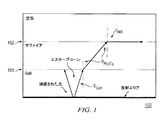
図1は、光がLED構造100の異なる媒質を通して移動する様式を示した概略図である。図1の例では、窒化ガリウム(GaN)とサファイアとの間の第1の境界(界面101)、およびサファイアと空気との間の第2の境界(界面102)がある。サファイアの屈折率がずっと低いため、いくつかの光子は、より高い屈折率を有する放射材料内に捕捉される。放射材料内に捕捉された光の量は、LEDの光抽出効率に反比例する。GaN材料内に捕捉された光が多いほど、LEDの効率は低い。本明細書に開示された完全エミッタ層成形(CELS)プロセスの実施形態に従い放射材料を成形すると、GaNから放出された光がサファイア基板に逃げ、最終的にサファイアから空気に逃げるのを促進することができる。本明細書に開示された実施形態によれば、CELSプロセスは、エミッタ材料の成形により、任意の発光ダイオードの光抽出効率を最大化することができる。本明細書において、例示的な放射材料としてGaNが使用されているため、このプロセスはまたGaN成形とも呼ばれる。
FIG. 1 is a schematic diagram illustrating how light travels through different media of an
空気の屈折率を1と仮定すると、サファイアの屈折率は1.77、GaNの屈折率は2.5であり、したがってGaNにおける出射角は以下のように計算することができる。 Assuming that the refractive index of air is 1, the refractive index of sapphire is 1.77, and the refractive index of GaN is 2.5. Therefore, the emission angle in GaN can be calculated as follows.

エスケープコーンは、全放出光のごくわずかである。失われたエネルギー量を計算するために、均等拡散エミッタに対するエスケープコーンの投射立体角を計算する。均等拡散エミッタの立体角はPiステラジアンである。23.58度のエスケープコーンの立体角は、 The escape cone has very little total emitted light. In order to calculate the amount of energy lost, the projected cone angle of the escape cone for the uniform diffuse emitter is calculated. The solid angle of the uniform diffuse emitter is Pi steradians. The solid angle of the escape cone of 23.58 degrees is
産業において、多くはLED構造内の高屈折率から低屈折率への様々な界面でTIRを妨害または制限する手法に焦点を置いているが、本明細書で開示された実施形態は、これらの界面においてTIRが存在する理由に焦点を置いている。TIRは、輝度のために生じる。輝度の定理は、放射輝度保存定理とも呼ばれるが、光学に適用されるエネルギー保存の定理である。放射輝度保存定理は、系の放射輝度が保存されなければならないことを述べている。 In the industry, many have focused on techniques for interfering or limiting TIR at various interfaces from high to low index in LED structures, but the embodiments disclosed herein are not limited to these. The focus is on why TIR exists at the interface. TIR occurs because of luminance. The luminance theorem is also called a radiance conservation theorem, but is an energy conservation theorem applied to optics. The radiance conservation theorem states that the radiance of the system must be preserved.
放射輝度保存定理は以下の通りである。 The radiance conservation theorem is as follows.
高屈折率材料における小さいエミッタエリアからより低屈折率のより大きなエリアへの移行において、側壁は、全反射を利用するように成形される。量子井戸領域から放出された光は、全反射により側壁で反射してより大きなエリアに向かう。エミッタから発するすべての放射線(または設計により決定されるある量の放射線)は、臨界角より大きい角度で側壁に衝突し、内部反射する。出口に衝突する放射線は、好ましくは臨界角未満の角度であり、放出面を通してより低い屈折率の材料における大きな領域へと通過する。したがって、システム輝度は、側壁により画定される光学システムにより保存される。 In the transition from a small emitter area in a high refractive index material to a larger area of lower refractive index, the sidewall is shaped to take advantage of total internal reflection. The light emitted from the quantum well region is reflected by the side wall by total reflection and travels to a larger area. All radiation (or a certain amount of radiation determined by design) emanating from the emitter strikes the sidewall at an angle greater than the critical angle and is internally reflected. The radiation impinging on the exit is preferably at an angle less than the critical angle and passes through the emission surface to a large area in the lower refractive index material. Thus, system brightness is preserved by the optical system defined by the sidewalls.
ベース基板がサファイアであり、放射材料がGaNであり、所望の出射角が90度均等放散であると仮定すると、放出面積は輝度の定理[式3]により計算することができる。上述の式3aはまた、放出面積のずれを示している。入射面積に対する放出面積の比率は、屈折率の比の2乗に等しい。一例として、屈折率が2.5であり、または終端媒質が空気であるエミッタ媒質の場合、放出面積は入射面積の2.5倍の二乗に等しい。この例において、エミッタ面積に対する放出面積の比率は、6.25:1である。 Assuming that the base substrate is sapphire, the emissive material is GaN, and the desired emission angle is 90 degree uniform dissipation, the emission area can be calculated by the luminance theorem [Equation 3]. Equation 3a above also shows the deviation of the emission area. The ratio of the emission area to the incident area is equal to the square of the ratio of the refractive index. As an example, in the case of an emitter medium with a refractive index of 2.5, or the termination medium being air, the emission area is equal to the square of 2.5 times the incident area. In this example, the ratio of the emission area to the emitter area is 6.25: 1.
図2Aおよび2Bは、成形部分10および成形側壁60、65を備える、正方形エミッタ20の例示的実施形態の図表示の上面図および側面図である。いくつかの実施形態において、放出面55は、製造プロセスの許容差内で、界面50と実質的に同じ形状、実質的に平行および実質的に回転整列してもよい。いくつかの実施形態において、放出面55の形状は、界面50の形状とは異なっていてもよい。
2A and 2B are top and side views of a graphical representation of an exemplary embodiment of a
放出面55の面積は、輝度の定理[式3]による輝度を保存するように選択され得る。以下の式3bは、放出面積の例示的なずれを示している。
The area of the
Φ2=放出面55を出る光束、輝度の保存のためにはΦ1=Φ2、
Ω1=光が界面50を横断する有効立体角、
Ω2=光が放出面55を出る有効立体角、
A1=界面50の面積、
A2=放出面55の面積、
n1=基板10の材料の屈折率、
n2=基板10の外部の基板(例:空気またはその他の媒質)の屈折率。
Φ 2 = luminous flux exiting the
Ω 1 = effective solid angle at which light crosses
Ω 2 = the effective solid angle at which light exits the
A 1 = area of
A 2 = area of
n 1 = refractive index of the material of the
n 2 = refractive index of a substrate external to the substrate 10 (eg, air or other medium).
A2は、光が上記式に従い保存されるような放出面55の最小表面積を表す。例えば、界面50が約1mm四方の面積を有するように量子井戸領域15が1mm四方を形成し、n1=1.77、n2=1、Ω1=3、Ω2=1、およびファイ1がファイ2に等しいと仮定すると、放射輝度を保存するにはA2は少なくとも9.3987mm2でなければならない。この例では、有効立体角Ω1およびΩ2、n1およびn2、ファイ1およびファイ2が与えられる。有効立体角の決定に関するさらなる教示については、2007年10月1日出願の上述の米国特許出願第11/906,219号および第11/906,194号、名称「LED SYSTEM AND METHOD」を参照されたい。
A 2 represents the minimum surface area of the
A2は、放射輝度の保存のための放出面55の最小表面積および所与の出力円錐角または放出半角に対する可能な限り最小のサイズを表す。いくつかの実施形態において、A2は、製造プロセスにおける許容差、量子井戸領域のサイズもしくは形状またはその他の因子における誤差を補償するために若干より大きくされてもよい。A2がこのように決定された最小値よりも大きくされた場合、光束は保存されるが、発散(単位面積あたりの光束として定義される)は、達成可能な最大値から低下し得る。
A 2 represents the minimum surface area of the
デバイスの高さは、システムにおける制限放射線により決定され得る。この放射線は、高屈折率材料内の最長距離を横断する。放出面が正方形である場合、対角線の放射線が制限放射線である。図2Aおよび2Bに示される例では、放出面40が正方形であるため、対角線の放射線45が制限放射線である。
The height of the device can be determined by the limiting radiation in the system. This radiation traverses the longest distance in the high index material. If the emission surface is square, the diagonal radiation is the limiting radiation. In the example shown in FIGS. 2A and 2B, since the
1辺が1で面積が1平方単位の単位エミッタおよび1辺が2.5で面積が6.25である出口エミッタの場合、デバイスの最小高さは以下のように計算され得る。 For a unit emitter with a side of 1 and an area of 1 square unit and an exit emitter with a side of 2.5 and an area of 6.25, the minimum height of the device can be calculated as follows:
様々な実施形態によれば、LEDのエミッタ層の一部が上述のように成形されている。より具体的には、エミッタ層は、エミッタ層材料が基板と概して連続的に接触するように、基板(上述のようにサファイアであってもよい)に対する制御された深さまたは高さに成形される。したがって、いくつかの実施形態において、エミッタ材料の連続層は基板と接触し得る。いくつかの実施形態において、エミッタ材料の連続層は、基板と電気的に接触し得るか、または基板と電気面もしくは連続的な電気接続を形成する。いくつかの実施形態において、エミッタ層の一部のみが成形される。いくつかの実施形態において、エミッタ層は、制御された深さまたは高さに成形され得る成形部分および非成形部分または領域を備えてもよい。 According to various embodiments, a portion of the LED's emitter layer is shaped as described above. More specifically, the emitter layer is shaped to a controlled depth or height relative to the substrate (which may be sapphire as described above) such that the emitter layer material is generally in continuous contact with the substrate. The Thus, in some embodiments, a continuous layer of emitter material can be in contact with the substrate. In some embodiments, the continuous layer of emitter material may be in electrical contact with the substrate or form an electrical surface or continuous electrical connection with the substrate. In some embodiments, only a portion of the emitter layer is shaped. In some embodiments, the emitter layer may comprise molded and non-molded portions or regions that can be molded to a controlled depth or height.
エミッタ層と基板との間の界面の面積は、上述のように選択することができ、エミッタ層材料の高さは、エミッタ層の成形部分における最長距離または近似最長距離を横断する1つ以上の制限放射線に基づき選択することができる。具体例として、図2Aは、制御された高さ(h)に成形されたエミッタ20の成形部分10を示す。この例では、成形部分は、エミッタ層、例えばGaN層または他のエミッタ層等であってもよいが、これらに限定されない。エミッタ層材料20の非成形部分は図2Aには示されない。一実施形態において、上述の制限放射線は、エミッタ層の成形部分おける最長距離または近似最長距離を横断する。したがって、図2Aの例において、制限放射線45は、概してエミッタ層の成形部分の深さまたは高さ(h)で終端するように選択され得る。
The area of the interface between the emitter layer and the substrate can be selected as described above, and the height of the emitter layer material can be one or more that traverse the longest or approximate longest distance in the shaped portion of the emitter layer. Can be selected based on limiting radiation. As a specific example, FIG. 2A shows the shaped
一実施形態において、側壁の形状は経験的に決定される。側壁には以下の2つの制限がある:
a.側壁に衝突するエミッタから発するすべての放射線は、臨界角以上の角度で側壁に衝突すべきである。
b.側壁で反射するすべての放射線は、出口表面に向かって反射すべきであり、出口表面における入射角は臨界角未満である必要がある。
In one embodiment, the sidewall shape is determined empirically. There are two restrictions on the side wall:
a. All radiation emanating from the emitter impinging on the sidewall should impinge on the sidewall at an angle greater than the critical angle.
b. All radiation that reflects off the sidewall should be reflected towards the exit surface and the angle of incidence at the exit surface should be less than the critical angle.
側壁の形状の他の基準は、放出面における光の強度の均一性もしくは無限大でのガウス分布、または両方、またはその他の組の条件であってもよい。したがって、側壁は、放出された光が所望の強度または角度で基板に誘導されるのを確実とするように成形することができ、所望の強度または角度は、基板の特性、例えば基板、エミッタ材料または他の材料の屈折率等に基づいて決定され得る。 Other criteria for the shape of the sidewall may be light intensity uniformity at the emission surface or a Gaussian distribution at infinity, or both, or some other set of conditions. Thus, the sidewalls can be shaped to ensure that the emitted light is directed to the substrate at the desired intensity or angle, where the desired intensity or angle is a property of the substrate, eg, substrate, emitter material Alternatively, it can be determined based on the refractive index of other materials.
いくつかの実施形態において、側壁の形状は反復により決定することができる。形状は、n個のファセット(小平面)に分割される。側壁のファセットは、Microsoft Excel (MicrosoftおよびExcelは、ワシントン州レドモンドを拠点とするMicrosoft Corporationの商標である)等のコンピュータプログラムを使用して定義することができる。より具体的には、Microsoft Excelのグラフ機能を使用して、側壁の形状のグラフを作成することができる。各側壁に対し同じ一般形状を使用することができ、または異なる側壁に対し異なる形状を使用することができる。Excel等のプログラムを使用して、各ファセットのサイズおよび角度を変化させ、所望の性能を達成することができる。特定の側壁形状を有する(または特定のファセットに基づく湾曲側壁形状を有する)成形基板の立体モデルは、任意の機械製図プログラム、例えばSolidworks、AutoCad、Pro Engineer等を使用して作成することができる。立体モデルはまた、任意のレイ・トレーシングプログラム、例えばZemax、TracePro、BRO、Lighttools等を使用して作成および分析することができる。 In some embodiments, the sidewall shape can be determined iteratively. The shape is divided into n facets (small planes). Sidewall facets can be defined using a computer program such as Microsoft Excel (Microsoft and Excel are trademarks of Microsoft Corporation based in Redmond, Washington). More specifically, a graph of the shape of the sidewall can be created using the Microsoft Excel graph function. The same general shape can be used for each side wall, or different shapes can be used for different side walls. A program such as Excel can be used to vary the size and angle of each facet to achieve the desired performance. A solid model of a molded substrate having a specific sidewall shape (or a curved sidewall shape based on a specific facet) can be created using any mechanical drawing program such as Solidworks, AutoCad, Pro Engineer, etc. A solid model can also be created and analyzed using any ray tracing program such as Zemax, TracePro, BRO, Lighttools, etc.
物理学において、レイ・トレーシングは、様々な伝播速度、吸収特性、および反射表面の領域を有するある系を通る波または粒子の経路を計算するための方法である。これらの状況下において、波面は、曲げられ、方向を変化され、または表面で反射し得るため、分析が複雑となる。レイ・トレーシングは、放射線と呼ばれる理想的な細いビームを個別量だけ媒質を通して繰り返し前進させることにより問題を解決する。単純な問題は、単純な数学を使用していくつかの放射線を伝播させることにより分析することができる。より詳細な分析は、コンピュータを使用して多くの放射線を伝播させることにより行うことができる。電磁放射線の問題に適用する場合、レイ・トレーシングは、多くの場合、その寸法が光の波長よりもずっと大きい物体を通して、またはその周りを光波が伝播する限り有効な、マクスウェル方程式の近似解に依存する。 In physics, ray tracing is a method for calculating the path of a wave or particle through a system with various propagation velocities, absorption characteristics, and areas of reflective surfaces. Under these circumstances, the wavefront can be bent, redirected, or reflected from the surface, complicating analysis. Ray tracing solves the problem by repeatedly advancing an ideal thin beam called radiation through the medium in discrete amounts. Simple problems can be analyzed by propagating some radiation using simple mathematics. A more detailed analysis can be performed by propagating more radiation using a computer. When applied to electromagnetic radiation problems, ray tracing is often an approximate solution to Maxwell's equations that is valid as long as light waves propagate through or around objects whose dimensions are much larger than the wavelength of the light. Dependent.
市販のレイ・トレーシングプログラムを使用してコンピュータシミュレーションを行い、レイトレースならびに強度および放射輝度分布プロファイルを生成することができる。得られた強度および放射輝度プロファイルが不満足な分布を有する場合、または成形基板の透過効率が低すぎる場合、様々なファセットの変数を調整し、再びシミュレーションを行うことができる。このプロセスは、ファセット変数を自動的に調整するためのコンピュータプログラムを使用することにより自動化することができる。例示のため、以下の例はZemax光学設計プログラム(Zemaxはワシントン州ベルビューのZemax Development Corporationの商標である)を使用している。 Computer simulations can be performed using commercially available ray tracing programs to generate ray tracing and intensity and radiance distribution profiles. If the resulting intensity and radiance profiles have an unsatisfactory distribution, or if the transmission efficiency of the molded substrate is too low, various facet variables can be adjusted and the simulation performed again. This process can be automated by using a computer program to automatically adjust facet variables. For illustration purposes, the following example uses the Zemax optical design program (Zemax is a trademark of Zemax Development Corporation of Bellevue, Washington).
(Zemaxモデル)
輝度の式により決定付けられたサイズ制約を満たす形状が作成され、制限放射線に対する考慮がなされたら、レイ・トレーシングプログラムにおいてモデル化することができる。レイ・トレーシングプログラムは、その形状を通過する放射線をモデル化し、その効率、近視野および遠視野分布を決定する。
(Zemax model)
Once a shape that satisfies the size constraints determined by the luminance equation is created and considered for limiting radiation, it can be modeled in a ray tracing program. The ray tracing program models the radiation passing through the shape and determines its efficiency, near field and far field distribution.
図3は、成形側壁60、65を有する成形部分10の例示的立体モデルの側面図である。側壁60、65を有する部分10は、正方形エミッタ20のエミッタ層の成形部分を表している。具体例として、部分10は、屈折率2.5のGaN材料で代表される。出力分布は均等拡散である。
FIG. 3 is a side view of an exemplary three-dimensional model of molded
図4は、図3の立体モデルを通したレイ・トレーシングの一例である。TIRに起因して、放射線70は側壁60、65で反射して出口表面55に向かい、そこで屈折して放出面55を通過する。
FIG. 4 is an example of ray tracing through the solid model of FIG. Due to TIR, the
図5は、Zemaxで作成された立体モデルのスクリーンショットであり、例示的正方形エミッタ20の出口検出器面40での放射輝度を示している。任意のエッジ効果放射線が正確に記録されることを確実とするために、検出器面は放出面よりも大きく作製されている(この場合10単位×10単位)。放射輝度は、検出器面40の部分の中心を含んでいる。GaN材料の場合、図5は、GaN出口における近視野分布を示している。
FIG. 5 is a screen shot of a stereo model created with Zemax, showing the radiance at the
図6は、図5の立体モデルの別のスクリーンショットであり、検出器面40での放射強度を示している。放出面での放射強度は、遠距離での放射輝度と等しく、しばしば遠視野分布と呼ばれる。GaN材料の場合、図6は、GaNの後の遠視野分布を示している。
FIG. 6 is another screen shot of the three-dimensional model of FIG. 5 and shows the radiation intensity at the
図5および6は、成形されたLEDの一実施形態の光を空気中に出す効率を例示している。この場合、放出された光の約94%が、エミッタ層から抽出される。これは、異なる材料の層内の吸収損失およびフレネル損失を考慮していない。サファイア中の吸収損失は無視でき、GaN層は非常に薄い。いくつかの実施形態において、GaN層は、約4〜5ミクロンの厚さとなり得る。フレネル損失は以下の通りである。 Figures 5 and 6 illustrate the efficiency of emitting one embodiment of a molded LED into the air. In this case, about 94% of the emitted light is extracted from the emitter layer. This does not take into account absorption losses and Fresnel losses in layers of different materials. Absorption loss in sapphire is negligible and the GaN layer is very thin. In some embodiments, the GaN layer can be about 4-5 microns thick. The Fresnel loss is as follows.
基板の放出面における反射防止被覆の追加により、空気に対するサファイアのフレネル損失は排除され得る。したがって全効率は以下のようになる。 By adding an anti-reflective coating on the emission surface of the substrate, sapphire Fresnel loss to air can be eliminated. The overall efficiency is therefore:
![]()
正方形エミッタは、空間の無駄なく互いに完璧に適合するという利点を有する。また、ダイスカット操作が単純化され、2つの直交した切断だけとなる。正方形エミッタに関するさらなる教示については、2007年10月1日出願の上述の米国特許出願第11/906,219号および第11/906,194号、名称「LED SYSTEM AND METHOD」を参照されたい。正方形プロファイルは、等しい長さの辺を有する長方形プロファイルであることに留意されたい。以下の例示的実施形態において六角形エミッタが説明されているが、本明細書に開示された方法論は様々な形状に適用することができ、いかなる特定の形状、サイズ、構成、または材料によっても限定されないことが、当業者に理解される。
![]()
Square emitters have the advantage that they fit perfectly together without wasting space. Also, the die cutting operation is simplified and only two orthogonal cuts are made. For further teaching regarding square emitters, see the aforementioned US patent application Ser. Nos. 11 / 906,219 and 11 / 906,194, filed Oct. 1, 2007, entitled “LED SYSTEM AND METOD”. Note that a square profile is a rectangular profile with equal length sides. Although hexagonal emitters are described in the following exemplary embodiments, the methodology disclosed herein can be applied to a variety of shapes, limited by any particular shape, size, configuration, or material. It will be understood by those skilled in the art that this is not the case.
六角形パターンは、いかなる空間の無駄もなく互いに適合し得る。成形されたデバイスにおいて、六角形パターンは、正方形デバイスよりも少ない材料体積を提供し得る。図7A〜7Dは、六角形エミッタ720の一実施形態の様々な面の図表示を示す。
The hexagonal patterns can fit together without any space waste. In molded devices, the hexagonal pattern can provide less material volume than square devices. 7A-7D show diagrammatic representations of various surfaces of one embodiment of a
面積比は輝度の式により決定付けられ、したがってエミッタ面積(750)に対する放出面積(755)は、6.25:1の比を維持する。しかしながら、高さ(h)は、以下のように低減される。 The area ratio is determined by the luminance equation, so the emission area (755) to the emitter area (750) maintains a ratio of 6.25: 1. However, the height (h) is reduced as follows.
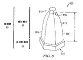
これらのベース単位寸法を使用して、立体モデルを作成しモデル化することができる。例えば、ProEで立体モデルを作成し、次いでZemaxでモデル化することができる。図8は、エミッタ層80を成形することにより作成された六角形エミッタ820の一実施形態の図表示である。この例において、エミッタ層80は、成形部分81および非成形部分82を備える。成形部分81において、基板810ならびに側壁860および865は、光抽出効率を最大化するために上述のような制御された高さhに成形され、最小のエネルギー損失で、界面850を通って基板810に入射し、放出面855を通って出る、量子井戸領域815からの光子を許容する。量子井戸領域に関するさらなる教示については、2007年10月1日出願の上述の米国特許出願第11/906,219号および第11/906,194号、名称「LED SYSTEM AND METHOD」を参照されたい。
These base unit dimensions can be used to create and model a stereo model. For example, a stereo model can be created with ProE and then modeled with Zemax. FIG. 8 is a diagrammatic representation of one embodiment of a
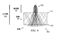
図9は、エミッタ層80を含む複数の層920を有するLED900の一実施形態の図表示である。エミッタ層80から放出された光は、界面101を通って基板90に入射し、界面102を通って基板90から空気中に出る。一実施形態において、基板90はサファイアである。六角形エミッタ820の効率は、Zemaxで分析された立体モデルによれば、約95.5%である。すなわち、放出された光の約95.5%が、エミッタ層から抽出される。フレネル損失を考慮すると、全抽出効率は約85%である。
FIG. 9 is a diagrammatic representation of one embodiment of an
(マイクロエミッタの配列)
GaN成形の1つの利点は、エミッタの大規模な配列を成形して1つのLEDを形成する能力である。別の利点は、微小なエミッタにより、除去される全体的な体積も減少することである。図12は、基板90、エミッタ層80、およびN接触層60を備えるLED120の一実施形態の図表示である。一実施形態において、基板90はサファイアである。一実施形態において、N接触層60は、1つ以上のN接触点を備える。一実施形態において、エミッタ層80は、六角形形状のマイクロLEDの配列を備える。一実施形態において、エミッタ層80は、六角形形状のマイクロLEDのM×M配列を備える。一実施形態において、LED 120は、約100ミクロン(W)×100ミクロン(L)×80ミクロン(D)である。図12の例において、六角形形状のマイクロLEDの配列は、エミッタ層80を成形することにより形成される。開示されたシステムおよび方法の実施形態は、任意の基板を使用することができ、それでも放出された光子のすべてまたはほぼすべてを抽出することができる。この例のためにベース基板はサファイアであるが、他の基板が使用されてもよい。
(Array of microemitters)
One advantage of GaN molding is the ability to mold a large array of emitters to form a single LED. Another advantage is that the microemitter also reduces the overall volume removed. FIG. 12 is a diagrammatic representation of one embodiment of an
上述のように、エミッタ層の成形部分は、概して基板と連続的に接触しており、電気面またはほぼ連続的な電気接続を形成する非成形部分に移行する。N接点は、電気面を形成するエミッタ層の非成形部分と電気的に接続しており、したがって、エミッタ層の非成形部分を通ってエミッタ層の成形部分に電流が流れるようにする。一実施形態において、N接点は、基板の成形および非成形部分を電源に電気的に結合し得る、金属合金等の導電材料であってもよい。 As described above, the shaped portion of the emitter layer is generally in continuous contact with the substrate and transitions to an unshaped portion that forms an electrical surface or a substantially continuous electrical connection. The N-contact is in electrical connection with the non-shaped portion of the emitter layer that forms the electrical surface, thus allowing current to flow through the non-shaped portion of the emitter layer to the shaped portion of the emitter layer. In one embodiment, the N-contact may be a conductive material, such as a metal alloy, that can electrically couple the formed and non-formed portions of the substrate to a power source.
代替の実施形態において、エミッタ層の非成形部分は、端部において電源と結合されてもよく、あるいは、1つ以上の成形部分が電源に結合されてもよく、あるいは、上記または電流を供給するその他の方法もしくはシステムの任意の組み合わせが使用されてもよい。また、N接点よりも小型でより多数のP接点を電源に結合してもよい。 In alternative embodiments, the non-shaped portion of the emitter layer may be coupled to a power source at the end, or one or more shaped portions may be coupled to the power source, or provide a current or current. Any combination of other methods or systems may be used. Alternatively, a larger number of P contacts may be coupled to the power source than the N contacts.
上述の構造は、実装、熱放散、および照明の均一性の追加的な利点を有する。各マイクロLEDの逃げ角度は、各マイクロLEDの非常に小さいサイズと併せて、1つのデバイスからの射出放射線を多数の隣接したマイクロLEDの射出放射線と重複させながら、光はまだ基板の厚みの中に含有されたままとなるような角度である。光が基板の放出面に達する時には、多くのマイクロLEDからの光は平均化され、非常に均一な光出力プロファイルを形成する。いくつかの実施形態によれば、エミッタ層におけるマイクロLEDの数は、1つから数個、数千個、数百万個、またはそれを超える範囲であってもよい。 The structure described above has the additional advantage of implementation, heat dissipation, and illumination uniformity. The relief angle of each micro LED, combined with the very small size of each micro LED, allows the light emitted from one device to overlap with the radiation emitted from a number of adjacent micro LEDs, while the light is still within the thickness of the substrate. The angle is such that it remains contained. When light reaches the emission surface of the substrate, the light from many micro LEDs is averaged to form a very uniform light output profile. According to some embodiments, the number of micro LEDs in the emitter layer may range from one to several, thousands, millions, or more.
熱的観点から、各マイクロLEDの放出ベースは、マイクロLEDに電力を提供するとともにマイクロLEDの熱除去経路を提供するサブマウントに直接接合され得る。これは、本質的に優れた熱拡散を提供する。エミッタは互いから離れて広がっているため、熱密度もまた低減される。 From a thermal point of view, the emission base of each micro LED can be directly bonded to a submount that provides power to the micro LED and provides a heat removal path for the micro LED. This provides inherently good thermal diffusion. Since the emitters are spread away from each other, the heat density is also reduced.
同様に、P層への電力は、LEDの表面全体にわたる多数の小さい点で供給されるため、電力は、サブマウント上の金属化のほぼ連続的な面によりこれらの点に印加され得る。これは、優れた電流拡散を提供する。電流拡散は、デバイスから最大量の光出力を提供する上での既知の問題である。改善された電流拡散を達成するため、異なるレイアウトのP型およびN型GaNの多くの構成が当技術分野において使用されている。マイクロLED構造は、本質的にこの拡散を提供する。 Similarly, since the power to the P layer is supplied at a number of small points across the surface of the LED, power can be applied to these points by the nearly continuous surface of metallization on the submount. This provides excellent current spreading. Current spreading is a known problem in providing the maximum amount of light output from a device. Many configurations of different layouts of P-type and N-type GaN are used in the art to achieve improved current spreading. The micro LED structure inherently provides this diffusion.
より具体的には、N層の厚さはP層の厚さと比較して大きいため、N層における電流の拡散は、N層への比較的少ない接触点により達成される。図12に示されるように、例えば4つの場所でのN層への接触が、これを達成する1つの方法である。あるいは、N層は、中心点または配列の端部周囲のいくつかの点で接触され得る。 More specifically, since the thickness of the N layer is large compared to the thickness of the P layer, current spreading in the N layer is achieved with relatively few contact points to the N layer. As shown in FIG. 12, contact with the N layer, for example at four locations, is one way to achieve this. Alternatively, the N layer can be contacted at a central point or several points around the end of the array.
(構築方法)
(エッチング)
エッチングは、適切な形状を生成するために極めて制御された様式で基板材料を除去する化学的プロセスである。通常は、湿式エッチングおよび乾式エッチングの2種類のエッチング方法がある。湿式エッチングは、基板材料を除去するための液相エッチャントの使用を含む。乾式エッチング、プラズマエッチングおよび反応性イオンエッチングでは、イオンが形成され、基板上に与えられる。ここで、化学反応または粒子の運動量のいずれかに基づき、材料が基板から除去される。
(How to build)
(etching)
Etching is a chemical process that removes substrate material in a highly controlled manner to produce the proper shape. Usually, there are two types of etching methods, wet etching and dry etching. Wet etching involves the use of a liquid phase etchant to remove substrate material. In dry etching, plasma etching and reactive ion etching, ions are formed and applied on the substrate. Here, the material is removed from the substrate based on either chemical reaction or particle momentum.
基板材料(量子井戸領域を備える材料をさらに含み得る)のウエハから開始して、フォトレジストの特定のパターンがウエハの側面に堆積され得る。次いでこのウエハがエッチングされる。ウエハ上のフォトレジストで覆われた場所はエッチングされず、一方フォトレジストのない場所は材料が除去される。フォトレジストの端部の所望の輪郭を達成するためにプロセスを調整する多くの手法がある。例えば、より厚い層のフォトレジストを施し、次いでエッチングプロセスの間犠牲的に除去することが可能であり、またはその他の犠牲層をフォトレジストと併用することができる。これらの層は、LED基板の所望の輪郭を生成するような様式でエッチャントにより経時的に除去される。これを利用して、成形基板を生成するためにウエハを正確にエッチングすることができる。別の手法は、複数のレジストおよび複数のエッチングステップを使用することである。エッチングフォトレジストおよびエッチングステップは、材料の小さな層を除去するために使用することができる。複数の小さいステップを使用して、所望の3D形状を得ることができる。 Starting from a wafer of substrate material (which may further include materials with quantum well regions), a specific pattern of photoresist may be deposited on the side of the wafer. The wafer is then etched. Locations covered with photoresist on the wafer are not etched, while material is removed where there is no photoresist. There are many ways to tailor the process to achieve the desired contour at the edge of the photoresist. For example, a thicker layer of photoresist can be applied and then sacrificially removed during the etching process, or other sacrificial layers can be used in conjunction with the photoresist. These layers are removed over time by the etchant in a manner that produces the desired profile of the LED substrate. This can be used to accurately etch the wafer to produce a molded substrate. Another approach is to use multiple resists and multiple etching steps. Etching photoresist and etching steps can be used to remove small layers of material. Multiple small steps can be used to obtain the desired 3D shape.
エッチングパラメータは、基板材料に基づき得る。エッチング速度は、エッチャントおよび基板に依存して変動する。サファイアおよび炭化ケイ素等のLED用途において使用される基板材料の場合、反応性イオンエッチングを使用したエッチング速度は、毎分250nmから2.5μmの範囲となり得、これは商業的生産目的では遅い可能性がある。炭化ケイ素は、上記エッチング速度の上限にあり、一方サファイアは下限にある。 Etching parameters may be based on the substrate material. The etching rate varies depending on the etchant and the substrate. For substrate materials used in LED applications such as sapphire and silicon carbide, etch rates using reactive ion etching can range from 250 nm to 2.5 μm per minute, which can be slow for commercial production purposes There is. Silicon carbide is at the upper limit of the etching rate, while sapphire is at the lower limit.
いくつかの実施形態において、InGaN/GaN系表面構造GaN側壁の成形は、トロイダルレンズテンプレートを使用したCl2/BCl3/Arプラズマ中の複数段階乾式エッチングプロセスにより行うことができる。いくつかの実施形態において、n型およびp型GaNおよびInGaN層のこの乾式エッチングプロセスは、フォトレジストおよびNiフォトマスクを使用した誘導結合プラズマ反応性イオンエッチング(ICP−RIE)により行うことができる。一定のICP/バイアス電力すなわち300/100Wおよび4mTorrチャンバ圧力で0.5nm未満の下限エッチング表面粗度を維持するために、Cl2/BCl3/Arの制御されたガス流速を使用することができる。低い流速(Cl2/BCl3/Ar)のガス混合物を使用した30mTorr、300W ICP、100Wバイアス電力では、n型GaNに対し12,000A/minのエッチング速度が予想される。複数段階エッチングプロセスの間、GaN側壁の下限表面粗度を維持するように注意が必要である。一例として、100Wのバイアス電力で1nm未満の低い二乗平均平方根(rms)粗度値が維持されるべきである。 In some embodiments, InGaN / GaN-based surface structure GaN sidewall molding can be performed by a multi-step dry etching process in a Cl 2 / BCl 3 / Ar plasma using a toroidal lens template. In some embodiments, this dry etching process of n-type and p-type GaN and InGaN layers can be performed by inductively coupled plasma reactive ion etching (ICP-RIE) using a photoresist and a Ni photomask. A controlled gas flow rate of Cl 2 / BCl 3 / Ar can be used to maintain a lower etch surface roughness of less than 0.5 nm at constant ICP / bias power, ie 300/100 W and 4 mTorr chamber pressure. . At 30 mTorr, 300 W ICP, 100 W bias power using a low flow rate (Cl 2 / BCl 3 / Ar) gas mixture, an etch rate of 12,000 A / min for n-type GaN is expected. Care must be taken to maintain the lower surface roughness of the GaN sidewall during the multi-step etching process. As an example, a low root mean square (rms) roughness value of less than 1 nm should be maintained with 100 W bias power.
InGaN/GaN系構造のテーパ型壁のエッチングの場合、GaNの滑らかな鏡面状ファセットを達成するためには、比較的高いCl2流速および低いチャンバ圧力約4mTorrが保たれるべきである。エッチングされたファセットのテーパ形状は、その選択されたパラメータに常に依存するため、ICP電力およびチャンバ圧力の最適化は慎重に行われるべきである。当業者に理解されるように、適切なエッチングパラメータを使用して、n−GaNの鏡面状側壁ファセットを得ることができ、これは、InGaN/GaN系発光ダイオードの製造に使用することができる。さらに、固定ガス流量において、または比較的低いICP/バイアス電力およびチャンバ圧力において、InGaN系材料のテーパ型側壁形状をさらに改善および改良することができる。 In the case of InGaN / GaN-based tapered wall etching, a relatively high Cl 2 flow rate and a low chamber pressure of about 4 mTorr should be maintained in order to achieve a smooth specular facet of GaN. Since the tapered shape of the etched facet always depends on its selected parameters, optimization of ICP power and chamber pressure should be done carefully. As will be appreciated by those skilled in the art, n-GaN specular sidewall facets can be obtained using suitable etching parameters, which can be used in the manufacture of InGaN / GaN based light emitting diodes. Furthermore, the tapered sidewall shape of InGaN-based materials can be further improved and improved at fixed gas flow rates or at relatively low ICP / bias power and chamber pressure.
図13は、基板90、およびエミッタ層80の成形部分81に形成された六角形エミッタ820の配列を有するエミッタ層80を備えるLED130の一実施形態の図表示である。図13に示されるように、エミッタ層の一部または層は、エミッタ層材料を除去して、上記図8に示されるような成形側壁を有し得るμLEDエミッタの配列を形成することにより成形される。より具体的には、エミッタ層80は、基板90に対し制御された深さまたは高さに成形され、エミッタ820間のエッチング溝131および基板90に隣接するエミッタ層材料80のほぼ連続的な非成形層82を残している。一実施形態において、各エッチング溝131は、約0.4ミクロンの幅である。すなわち、この例において、マイクロLED820は、最も狭い点において約0.4ミクロンだけ離間し得る。
FIG. 13 is a diagrammatic representation of one embodiment of an
図13において、基板90に隣接するエミッタ層80の非成形部分82は、連続N−GaN層132を形成し、そこで非成形エミッタ層材料は概して基板と連続的に接触する。したがって、一実施形態において、概して基板と接触し、電気的に接触するか、または電気面もしくは連続的な電気接続を形成するエミッタ層材料の連続層があってもよい。一実施形態において、すべてのまたは概してすべてのエミッタ層材料が成形されるわけではないため、制御された深さまたは高さに成形され得るエミッタ層の成形部分、および成形されない(エミッタ層材料の)エミッタ層の非成形部分が存在する。一実施形態において、上述の制限放射線は、エミッタ層の成形部分おける最長距離または近似最長距離を横断する(すなわち、制限放射線は成形されたマイクロLEDエミッタを横断し得る)。したがって、制限放射線は、基板に対するエミッタ層の成形部分の深さまたは高さで概して終端するように選択され得る。上でさらに説明されているように、エミッタ層材料(例えば、マイクロLEDエミッタの側壁)は、エミッタ層の成形部分における最長距離または近似最長距離を横断する1つ以上の制限放射線に基づき成形され得る。
In FIG. 13, the
(複数段階式メサエッチングプロセス)
図14は、複数段階式メサエッチングプロセスの一実施形態の図表示である。本開示内において、「メサ」は、エッチング後に残留し、「メサ」として表れデバイスの発光部分となるものを形成するウエハの部分である。ステップ141において、エミッタ層80は、エッチング溝131の底部を画定するようにパターン化される。ステップ142において、等方性のエッチング化学薬品を使用して直立またはほぼ直立した側壁を達成する。ステップ143において、エミッタ層80は、エッチング溝131の頂部を画定するように再びパターン化される。ステップ144において、異方性のエッチング化学薬品を使用して側壁に局面を形成する。いくつかの実施形態において、続く処理は金属化および不動態化を含み得る。様々な実施形態において、複数のフォトおよびエッチングステップを使用して、発光層の最終プロファイルをより良く精密化することができる。エッチング化学は、側壁プロファイルを直線(等方性)から曲面(異方性)に変化させるように選択することができる。これは、湾曲形状を形成するための単一ステップを通して、または発光層の側壁形状に様々なファセットをエッチングするための複数のステップにおいて行うことができる。製造ステップの順番は、所望により変動し得る。例えば、メサの頂部が最初に画定され、続いてフォトエッチングが行われてもよい。ステップは、表面構造においてより深くエッチングしてもよい。
(Multi-stage mesa etching process)
FIG. 14 is a diagrammatic representation of one embodiment of a multi-step mesa etching process. Within this disclosure, a “mesa” is that portion of the wafer that remains after etching and forms what appears as a “mesa” and becomes the light emitting portion of the device. In step 141,
図14の例において、LED140の一実施形態は、上述の複数段階式メサエッチングプロセスにより製造され得る。この例において、LED 140は基盤90およびエミッタ層80を備える。この例において、エミッタ層80は、上述の複数段階式メサエッチングプロセスにより形成される成形部分81を備え、エミッタ層80の非成形部分82は基板90に隣接したままとなっている。複数段階式メサエッチングプロセスのパターン化およびエッチングステップは、エミッタ820間にエッチング溝131を形成する。図8を参照して上述したように、各エミッタ820は、成形側壁860を有する成形基板810および量子井戸領域815を備えてもよい。成形基板810は、放射材料でできている。一実施形態において、放射材料はGaNである。一実施形態において、基板90はサファイアである。
In the example of FIG. 14, one embodiment of
また、他のエッチングプロセスを使用してLED140を生成することができる。例えば、エミッタ層を成形するための方法の一実施形態は、基板上にp層金属を堆積させるステップと、p層金属上に反射層を堆積させるステップと、反射層上にSiO2保護層(緩衝層)を堆積させるステップと、堆積させた層を所望の形状にエッチングするステップと、次いでn層金属を堆積させるステップとをこの順番で含み得る。別の例として、エミッタ層を成形するための方法の一実施形態は、マスクAパターンを堆積させるステップと、マスクAパターンに従い不要な材料をエッチングで除去するステップと、マスクBパターンを堆積させるステップと、マスクBパターンに従いさらなる材料をエッチングで除去するステップと、パターン化−エッチングステップを繰り返して所望の高さを構築するステップと、n層金属を堆積させ、n層金属の上にp層金属を堆積させ、最後に反射層を堆積させるステップとをこの順番で含み得る。
Also, other etching processes can be used to produce the
いくつかの実施形態は、直立側壁を得るための等方性エッチングステップを省略し、一実施形態においてGaNを含む放射材料の成形に直接進んでもよい。例えば、エミッタ層を成形するための方法の一実施形態は、p層金属で基板をブランケット被覆するステップと、p層金属で被覆された基板をフォトレジストパターン化するステップと、それに従い不要な材料をエッチングで除去するステップとをこの順番で含み得る。一実施形態において、ICP−RIEを利用してエミッタ層から不要な材料をエッチングで除去する。また、他のエッチング方法が使用されてもよい。 Some embodiments may skip the isotropic etching step to obtain upstanding sidewalls and proceed directly to shaping of a radiant material comprising GaN in one embodiment. For example, one embodiment of a method for forming an emitter layer includes blanket coating a substrate with p-layer metal, photoresist patterning a substrate coated with p-layer metal, and unnecessary material accordingly Etching in this order. In one embodiment, ICP-RIE is used to etch away unwanted material from the emitter layer. Other etching methods may also be used.
この方法は、単一マスクGaNプロファイルのみを使用し、このようにして形成されたp接点は硬質マスクとして使用され、メサに整合しなおす必要性を回避し、フォトレジストパターン化ステップを排除している。塩素(Cl2)および三塩化ホウ素(BCl3)ガスの濃度を変化させることにより、異なるGaNエッチング勾配を得ることができる。より具体的には、いくつかの実施形態において、GaN材料がエッチングされている間、局所勾配に影響を与えるためにCl2およびBCl3濃度の比率を変化させる一連のステップが行われる。例えば、より高い濃度のCl2またはCl2のみを使用して、より直立した側壁を得ることができる。BCl3を多く含む化学組成は、側壁を不動態化するポリマーを生成する。高さ=0で特定の勾配を得るために、Cl2およびBCl3プラズマは、特定の濃度比を有し得る。高さ=1で別の勾配を得るために、Cl2およびBCl3の濃度比を変化させることができる。所望の高さに達するまで、上記ステップを繰り返すことができる。エミッタ層の完全な高さにわたり、エッチングプラズマの濃度比に依存して、エミッタ層における各マイクロLEDの側壁の勾配は、非常に浅い角度から非常に急な角度まで移行し、このようにしてエミッタ層を成形することができる。 This method uses only a single mask GaN profile, the p-contact formed in this way is used as a hard mask, avoiding the need to re-align to the mesa, eliminating the photoresist patterning step Yes. By changing the concentration of chlorine (Cl 2 ) and boron trichloride (BCl 3 ) gases, different GaN etch gradients can be obtained. More specifically, in some embodiments, while the GaN material is being etched, a series of steps are performed to change the ratio of Cl 2 and BCl 3 concentrations to affect the local gradient. For example, only higher concentrations of Cl 2 or Cl 2 can be used to obtain more upstanding sidewalls. A chemical composition rich in BCl 3 produces a polymer that passivates the sidewalls. In order to obtain a specific gradient at height = 0, the Cl 2 and BCl 3 plasmas may have a specific concentration ratio. To obtain another gradient at height = 1, the concentration ratio of Cl 2 and BCl 3 can be varied. The above steps can be repeated until the desired height is reached. Over the full height of the emitter layer, depending on the concentration ratio of the etching plasma, the slope of the sidewalls of each micro LED in the emitter layer transitions from a very shallow angle to a very steep angle, thus the emitter The layer can be shaped.
いくつかの実施形態は、プロファイルされたGaNエッチングのために2種のマスキング材料での単一フォトレジストパターンを利用し得る。例えば、エミッタ層を成形するための方法の一実施形態は、以下の特徴を含み得る。
1)フォトレジストパターンは、最終GaN面積と比較してサイズが大きい。
2)さらなるプロファイル制御のために焦点/露光を利用して側壁に勾配をつけることができる。
3)硬質マスクに酸化物を使用する。一実施形態において、硬質マスクは、BOE/HFのいずれかにおいてエッチングされ得るか、六フッ化硫黄(SF6)プラズマエッチングされる。バッファード酸化物エッチング(BOE)は、酸化ケイ素のより制御されたエッチング速度を有する、フッ化アンモニウムおよびフッ化水素酸(HF)の混合である。
4)約1:1のレジストエッチング比、および約5:1の酸化物エッチング比を使用する。1:1エッチング比は、レジストが中間的なエッチングで消費されるようなレジスト厚さを標的とするように使用される。これは、GaNの事前に保護された領域を露出させる。
5)酸化物硬質マスクが約5:1の比でエッチングされ、エッチングの残りを堅牢にする。
6)Cl2およびBCl3の比の制御がまたプロファイル制御を補助し得る。
Some embodiments may utilize a single photoresist pattern with two masking materials for profiled GaN etching. For example, one embodiment of a method for forming an emitter layer may include the following features.
1) The photoresist pattern is large compared to the final GaN area.
2) The sidewall can be graded using focus / exposure for further profile control.
3) Use an oxide for the hard mask. In one embodiment, the hard mask can be etched either in BOE / HF or is sulfur hexafluoride (SF 6 ) plasma etched. Buffered oxide etching (BOE) is a mixture of ammonium fluoride and hydrofluoric acid (HF) with a more controlled etching rate of silicon oxide.
4) Use a resist etch ratio of about 1: 1 and an oxide etch ratio of about 5: 1. A 1: 1 etch ratio is used to target the resist thickness such that the resist is consumed in an intermediate etch. This exposes a pre-protected region of GaN.
5) The oxide hard mask is etched in a ratio of about 5: 1 to make the remainder of the etch robust.
6) Control of the ratio of Cl 2 and BCl 3 can also assist in profile control.
(機械的成形)
図14は、マイクロLEDの配列を形成する1つの方法を表し、例示的であり限定的ではなく、マイクロLEDの配列を形成するためのその他の方法が可能であり、本発明の範囲内である。いくつかの実施形態において、成形GaN材料を形成するための方法は、レーザを使用してGaN材料を切除し、所望の形状を形成して必要な滑らかさを提供するステップを含む。レーザアブレーションは、量子井戸領域または基板材料を除去または排出することにより、高出力レーザを使用してLEDを生成するステップである。各レーザパルスは、わずかな量の材料を除去するのみである。レーザは、各々のその後のパルスで材料を除去するように平行移動され得る。X−YおよびZ方向に平行移動することにより、3D形状が除去され得る。レーザアブレーションの実施形態は、エッチングよりも速く基板を成形するために使用することができる。既知の技術を使用して、レーザアブレーションは、炭化ケイ素およびサファイアにおいて、毎分約500μmから1mmの厚さを除去することができる。
(Mechanical molding)
FIG. 14 depicts one method of forming an array of micro LEDs, which is exemplary and not limiting, and other methods for forming an array of micro LEDs are possible and within the scope of the present invention. . In some embodiments, a method for forming a shaped GaN material includes the step of using a laser to ablate the GaN material to form a desired shape to provide the required smoothness. Laser ablation is the step of generating an LED using a high power laser by removing or ejecting the quantum well region or substrate material. Each laser pulse only removes a small amount of material. The laser can be translated to remove material with each subsequent pulse. By translating in the XY and Z directions, 3D shapes can be removed. Laser ablation embodiments can be used to shape a substrate faster than etching. Using known techniques, laser ablation can remove thicknesses of about 500 μm to 1 mm per minute in silicon carbide and sapphire.
他の方法は、水または油のジェット中の粒子を使用して材料の除去をもたらす液体ジェット切断を含む。水ジェットを使用してウエハを切除し、所望の形状の基板を形成することができる。水ジェットアブレーションの一実施形態において、水の短いパルスを使用して、ウエハを段階的に切除することができる。水のパルスを使用してウエハを切除するプロセスは、レーザアブレーションに関して上述したプロセスと同様となり得る。水ジェットアブレーションの一実施形態において、水ジェットを使用してある特定の角度でウエハを完全に切断し、次いで角度をわずかにずらして水ジェットを使用してわずかに大きい角度でウエハを切断し、最終的に所望の形状の基板を生成することができる。さらなる実施形態において、水ジェットに研削材(例:工業用ダイヤモンド粒子)を投入し、材料が切除される速度を増加させることができる。 Other methods include liquid jet cutting that uses particles in a water or oil jet to effect material removal. A wafer can be cut using a water jet to form a substrate of the desired shape. In one embodiment of water jet ablation, a short pulse of water can be used to ablate the wafer in stages. The process of ablating the wafer using a pulse of water can be similar to the process described above for laser ablation. In one embodiment of water jet ablation, the water jet is used to completely cut the wafer at a certain angle, then the angle is slightly shifted and the water jet is used to cut the wafer at a slightly larger angle, Finally, a substrate having a desired shape can be generated. In a further embodiment, abrasive material (eg, industrial diamond particles) can be injected into the water jet to increase the rate at which material is cut.
別の選択肢は、粉砕、フライス加工、切断、超音波粉砕、研磨、掘削、または機械的除去のその他のシステムもしくは方法により、材料を機械的に除去することである。機械的除去により材料を除去して1つ以上のLEDを成形するための数々の方法がある。材料のウエハを切除して所望の形状を形成する上記方法を個々に説明したが、上記方法を組み合わせてもよい。例えば、適切に湾曲した側壁形状を確実とするために、機械的除去および水ジェットアブレーションの組み合わせを使用することが可能となり得る。同様に、基板材料に依存して、必要に応じてウエハから基板材料を除去するための方法および技術の様々な他の組み合わせを使用することができる。一実施形態において、材料の機械的除去は、段階的に行うことができる。 Another option is to mechanically remove material by grinding, milling, cutting, ultrasonic grinding, polishing, drilling, or other systems or methods of mechanical removal. There are a number of ways to remove material by mechanical removal to shape one or more LEDs. While the above methods for cutting a wafer of material to form a desired shape have been described individually, the methods may be combined. For example, it may be possible to use a combination of mechanical removal and water jet ablation to ensure a properly curved sidewall shape. Similarly, depending on the substrate material, various other combinations of methods and techniques for removing the substrate material from the wafer can be used as needed. In one embodiment, the mechanical removal of material can be performed in stages.
超音波粉砕の実施形態において、1つ以上のLEDの逆の形状を有するツールに研削剤を下塗りし、材料が除去され成形された基板が生成されるように、ツールが超音波振動して基板材料上で磨く/擦る作用を生成している間に基板材料と接触させる。 In an ultrasonic grinding embodiment, the tool is ultrasonically vibrated so that the tool has one or more LED inverse shapes with an abrasive and the material is removed to produce a shaped substrate. Contact with the substrate material while creating a polishing / rubbing action on the material.
LED基板および側壁を成形するためのシステムおよび方法の追加的な例は、上述の2007年10月1日出願の米国特許出願第11/906,219および11/906,194、名称「LED SYSTEM AND METHOD」に記載されており、その両方ともすべての目的のために本明細書に完全に援用される。側壁を成形する様々な方法を、上述のような発光層に適用することができる。一例として、図15は、湾曲した側壁155を有する六角形幾何学構成のマイクロLED152の配列を備えるLED 150の一実施形態の図表示である。この例におけるLED150は、長方形形状である。しかしながら、他の形状も可能である。別の例として、図16は、基板161と、傾斜した側壁165を有する六角形幾何学構成のマイクロLED162の配列とを備えるLED 160の一実施形態の図表示である。さらに別の例として、図17は、基板171と、直立した側壁175を有する六角形幾何学構成のマイクロLED172の配列とを備えるLED 170の一実施形態の図表示である。
Additional examples of systems and methods for molding LED substrates and sidewalls are described in US patent application Ser. Nos. 11 / 906,219 and 11 / 906,194 filed Oct. 1, 2007, entitled “LED SYSTEM AND”. Both of which are fully incorporated herein by reference for all purposes. Various methods of forming the sidewall can be applied to the light emitting layer as described above. As an example, FIG. 15 is a diagrammatic representation of one embodiment of an
成長
いくつかの実施形態において、マイクロLEDはまた、エミッタ層を成長させることにより作製され得る。GaNを例にとると、GaN薄膜を成長させるための多くの一般的に使用されるプロセスの1つは堆積である。GaNは、多くの種類のエピタキシャル成長により、またSiCおよびサファイアを含むいくつかの基板上で成長されている。例示的なGaN成長法には、有機金属気相堆積法(MOCVD)、ヨウ素気相成長法(IVPG)、分子線エピタキシー法(MBE)、機械的スパッタエピタキシー法(MSE)、および水素化物気相エピタキシー法(HVPE)が含まれるが、これらに限定されない。
Growth In some embodiments, a micro LED can also be fabricated by growing an emitter layer. Taking GaN as an example, one of the many commonly used processes for growing GaN films is deposition. GaN has been grown by many types of epitaxial growth and on several substrates including SiC and sapphire. Exemplary GaN growth methods include metal organic chemical vapor deposition (MOCVD), iodine vapor deposition (IVPG), molecular beam epitaxy (MBE), mechanical sputter epitaxy (MSE), and hydride vapor phase. Epitaxy (HVPE) is included, but is not limited to these.
いくつかの実施形態において、LEDのエミッタ層を成形する方法は、小型エミッタとも呼ばれるマイクロLEDの放出エリア(b)およびエミッタエリア(a)を決定するステップを含んでもよく、放出エリア(b)は、第1の幾何学的構成において放出面を有し、エミッタエリア(a)は、第2の幾何学的構成において量子井戸領域を有する。放出エリア(b)およびエミッタエリア(a)を使用して、小型エミッタの最小高さ(h)を上述のように計算することができる。方法は、さらに、最小高さ(h)を満たす成形された部分を形成するように、第1の幾何学的構成、第2の幾何学的構成、および最小高さ(h)に従い、堆積により小型エミッタを成長させるステップを含む。1つ以上のマイクロLEDは、このように同時に生成され得る。いくつかの場合において、非成形部分もまた形成することができる。エミッタ層の非成形部分は、ベース基板に隣接する。サファイアは、好適なベース基板の一例である。小型エミッタの成長において、小型エミッタの側壁は、エミッタエリアからその側壁までの直線伝送路を有する放射線の少なくとも大部分を、放出面における臨界角以下の放出面における入射角で放出面に反射させるように位置付けられ、かつ成形される。いくつかの実施形態において、マイクロLEDはまた、当業者に知られた技術を使用してエミッタ相を成長および成形することにより作製され得る。いくつかの実施形態において、エミッタ層の成長および成形は、交互に、同時に、または概して同時に行うことができる。 In some embodiments, the method of shaping the emitter layer of the LED may include determining the emission area (b) and emitter area (a) of the micro LED, also referred to as a miniature emitter, where the emission area (b) The emitter area (a) has a quantum well region in the second geometric configuration. Using the emission area (b) and the emitter area (a), the minimum height (h) of the small emitter can be calculated as described above. The method further includes depositing according to the first geometric configuration, the second geometric configuration, and the minimum height (h) to form a shaped portion that satisfies the minimum height (h). Growing a small emitter. One or more micro LEDs can thus be generated simultaneously. In some cases, non-molded portions can also be formed. The non-molded portion of the emitter layer is adjacent to the base substrate. Sapphire is an example of a suitable base substrate. In the growth of small emitters, the sidewalls of the small emitters reflect at least most of the radiation having a linear transmission path from the emitter area to the sidewalls to the emission surface at an incident angle at the emission surface that is less than the critical angle at the emission surface. And molded. In some embodiments, the micro LED can also be fabricated by growing and shaping the emitter phase using techniques known to those skilled in the art. In some embodiments, the growth and shaping of the emitter layer can occur alternately, simultaneously, or generally simultaneously.
したがって、いくつかの実施形態において、LEDのエミッタ層を成形する方法により製造されるLEDは、ベース基板の表面上のエミッタ層を備え、エミッタ層は成形部分を有し、成形部分は、放出エリア(b)、エミッタエリア(a)、最小高さ(h)、および側壁を備え、放出エリア(b)は、第1の幾何学的構成において放出面を有し、エミッタエリア(a)は、第2の幾何学的構成において量子井戸領域を有し、最小高さ(h)は、放出エリア(b)およびエミッタエリア(a)を使用して決定され、側壁の各々は、エミッタエリアからその側壁までの直線伝送路を有する放射線の少なくとも大部分を、放出面における臨界角以下の放出面における入射角で放出面に反射させるように位置付けられ成形される。 Thus, in some embodiments, an LED manufactured by a method of molding an emitter layer of an LED comprises an emitter layer on a surface of a base substrate, the emitter layer having a shaped portion, the shaped portion being an emission area. (B), comprising an emitter area (a), a minimum height (h), and sidewalls, the emission area (b) having an emission surface in a first geometric configuration, the emitter area (a) being Having a quantum well region in the second geometry, the minimum height (h) is determined using the emission area (b) and the emitter area (a), each of the sidewalls extending from the emitter area to its It is positioned and shaped to reflect at least the majority of the radiation having a straight transmission path to the sidewalls to the emission surface at an incident angle at the emission surface that is less than or equal to the critical angle at the emission surface.
(用途)
成形された発光層を有するLEDは、様々な用途に使用することができる。そのような多用途性の1つの理由は、所望のLEDを形成するようにマイクロLEDが様々な様式で配置され得ることである。各々微小エミッタの配列を有するLEDもまた、所望の光量および所望の光パターンを生成するように配置され得る。例えば、マイクロLEDおよび/またはLEDは、正方形、長方形、円形、またはその他の形状に配置され得る。LEDの配列を使用して所望の光量を生成することは、単一のLEDを使用するよりも効率的となり得、またはより消費空間を少なくし得る。図14が例示するように、マイクロLEDの配列は、ウエハ材料が除去されてエッチング溝131およびエミッタ820が形成される同じウエハから形成され得る。上記実施形態は材料のウエハからマイクロLEDを形成することを説明しているが、LEDを生成するために利用される成形基板は、基板材料の棒状の塊から形成することができる。
(Use)
An LED having a molded light emitting layer can be used for various applications. One reason for such versatility is that the micro LEDs can be arranged in various ways to form the desired LEDs. The LEDs, each having an array of microemitters, can also be arranged to produce the desired amount of light and the desired light pattern. For example, the micro LEDs and / or LEDs may be arranged in a square, rectangular, circular, or other shape. Using an array of LEDs to produce the desired amount of light can be more efficient than using a single LED, or can consume less space. As FIG. 14 illustrates, the array of micro LEDs can be formed from the same wafer where the wafer material is removed to form the
いくつかの場合において、LEDを使用して白色光を生成することが望ましい可能性がある。これは、単一色(例:青)の短波長LEDからの光を、光を吸収して人間の目が白色光として認識する波長の光を再び放出するリン光体またはその他の粒子に衝突させることにより達成することができる。リン光体またはその他の粒子をLEDの実施形態と併用して白色光を生成することができる。 In some cases, it may be desirable to generate white light using an LED. This impinges light from a single color (eg blue) short wavelength LED on a phosphor or other particle that absorbs light and re-emits light of a wavelength that the human eye recognizes as white light. Can be achieved. Phosphors or other particles can be used in conjunction with LED embodiments to produce white light.
LEDの放出面(複数を含む)の被覆は、白色光LED製造の単純化を可能とし得る製造上の利点を有し得、一方これは白色光LED製造のコストを低減し得る。例えば、そこから成形基板LEDが形成されるウエハの面を、励起されて白色光を放出し得るリン光体またはその他の粒子を含有する層(すなわち粒子被覆)で被覆することができる。粒子被覆で被覆されていないウエハの面を切除することができる。ウエハが切除されて複数のLEDが生成される場合、LEDは、白色光を生成するために必要な粒子被覆を有する放出面を有する。さらに、成形基板は、基板に入射する光の圧倒的多数を既知の放出面(複数を含む)に誘導するため、特定の放出面(複数を含む)の被覆は、白色光の生成において極めて効果的となり得る。したがって、成形基板の使用は、LEDの側壁または側壁の一部を粒子被覆で被覆する必要性を排除し得る。このように、各LEDに個々に粒子被覆を塗布する必要性がなくなる。ウエハの1つの面に粒子被覆を塗布するのは、個々のLEDに粒子被覆を塗布するより安価となり得る。基板の側壁は、粒子被覆との相互作用により基板内に再び散乱した光が部分的または完全に再利用され得るように設計することができる。白色光を生成するためにLEDと併せてナノ粒子を利用すると、最小限の光の偏向を可能とし、したがって後方散乱光が最小限となり、放出面から放出される光が最大となる。 The coating of the emitting surface (s) of the LED may have manufacturing advantages that may allow for simplification of white light LED manufacturing, while this may reduce the cost of white light LED manufacturing. For example, the surface of the wafer from which the molded substrate LED is formed can be coated with a layer containing phosphor or other particles that can be excited to emit white light (ie, a particle coating). The surface of the wafer that is not coated with the particle coating can be excised. When the wafer is ablated to produce a plurality of LEDs, the LEDs have an emission surface with the necessary particle coating to produce white light. In addition, the molded substrate guides the overwhelming majority of light incident on the substrate to the known emission surface (s), so the coating of the specific emission surface (s) is extremely effective in generating white light Can be the target. Thus, the use of a molded substrate may eliminate the need to coat the LED sidewalls or portions of the sidewalls with a particle coating. In this way, there is no need to apply a particle coating to each LED individually. Applying a particle coating to one side of the wafer can be less expensive than applying a particle coating to individual LEDs. The sidewalls of the substrate can be designed so that light that is re-scattered into the substrate due to interaction with the particle coating can be partially or fully reused. Utilizing nanoparticles in combination with LEDs to generate white light allows for minimal light deflection, thus minimizing backscattered light and maximizing light emitted from the emitting surface.
LEDの実施形態の潜在的用途には、携帯電話表示用照明が含まれる。現在のシステムは、通常は、リン光体充填カプセル材料を有する3つの側方発光青色LEDを使用して白色光を生成する。LEDの側部は通常は不透明であり、生成された光の大きな割合が側壁により吸収される。これにより、光の50%超が吸収により失われることになる。さらに、空気に対するカプセル材の界面の屈折率の変化が、射出放射線が臨界角より大きい角度で界面に衝突するTIR条件を生成する。これにより、界面で約44%の損失となる。成形基板LEDの実施形態は、光導波路に生成された光の80%を供給することができ、これにより非常に大きなシステム輝度の改善が得られる。 Potential applications of LED embodiments include cell phone display lighting. Current systems typically generate white light using three side-emitting blue LEDs with phosphor-filled encapsulant material. The sides of the LED are usually opaque and a large percentage of the light generated is absorbed by the sidewalls. This causes more than 50% of the light to be lost due to absorption. Furthermore, the change in the refractive index of the capsule material interface to the air creates a TIR condition where the emitted radiation strikes the interface at an angle greater than the critical angle. This results in a loss of about 44% at the interface. Molded substrate LED embodiments can provide 80% of the light generated in the light guide, resulting in very large system brightness improvements.
LEDの実施形態の別の潜在的用途は、携帯電話カメラフラッシュとしての使用である。現在のシステムは、通常は、画像の中心部で非常に明るいエリアを、また端部で暗いエリアを生成するガウスエネルギー分布を有するLEDを使用しており、被写体の不均一な照明をもたらす。さらに、現在のフラッシュユニットのビーム形状は円形であり、CCDカメラにより撮影される画像は長方形である。さらに、空気に対するカプセル材の界面の屈折率の変化が、射出放射線が臨界角より大きい角度で界面に衝突するTIR条件を生成する。これにより、放出立体角の関数である界面での損失がもたらされる。一方、LEDの実施形態は、長方形または正方形のフラッシュを供給することができ、LEDの基板に入射する光の80%が均一な分布で画像エリアに提供される。これにより、従来技術のLEDフラッシュシステムとは対照的に、より均一な風景の照明およびより高レベルの照明が得られる。 Another potential use of the LED embodiment is as a mobile phone camera flash. Current systems typically use LEDs with a Gaussian energy distribution that produces a very bright area at the center of the image and a dark area at the edges, resulting in uneven illumination of the subject. Furthermore, the beam shape of the current flash unit is circular, and the image taken by the CCD camera is rectangular. Furthermore, the change in the refractive index of the capsule material interface to the air creates a TIR condition where the emitted radiation strikes the interface at an angle greater than the critical angle. This results in a loss at the interface that is a function of the emission solid angle. LED embodiments, on the other hand, can provide a rectangular or square flash, with 80% of the light incident on the LED substrate being provided in the image area with a uniform distribution. This provides more uniform landscape illumination and higher levels of illumination, as opposed to prior art LED flash systems.
LEDの実施形態の別の潜在的用途は、液晶ディスプレイ(「LCD」)の背景照明への用途である。従来のLCDシステムは、赤色、緑色および青色LEDの直線配列を使用する。LEDからの光は混合光導波路に誘導され、均一な色および強度を提供する。通常は、LEDは、LEDの上に設置されたドームを有し、光は楕円形の反射体に捕捉され、光が光導波路に誘導される。楕円形反射体は、点光源に対しては良好に機能するが、LEDは点光源ではなく、放射線のいくつかは光導波路内の焦点に届かない。さらに、ドームカプセル材からの一部の光は、180度を越える角度で放出され、光の一部は基板、PCBボードおよびその他の部品に吸収される。さらに、ドームは、ドームの空洞のサイズに対して大きいため、通常はある割合の光は屈折する。これらの損失は掛け算式であるため、実際に光導波路に届くのは最初にLEDから放出された光のわずかな割合である。 Another potential application of LED embodiments is for liquid crystal display ("LCD") background lighting. Conventional LCD systems use a linear array of red, green and blue LEDs. Light from the LED is directed into the mixed light guide, providing a uniform color and intensity. Typically, an LED has a dome placed on top of the LED, the light is captured by an elliptical reflector, and the light is guided to the light guide. Elliptical reflectors work well for point sources, but LEDs are not point sources and some of the radiation does not reach the focal point in the light guide. In addition, some of the light from the dome capsule material is emitted at an angle greater than 180 degrees, and some of the light is absorbed by the substrate, PCB board, and other components. Furthermore, because the dome is large relative to the size of the dome cavity, a proportion of light is usually refracted. Since these losses are multiplications, only a small percentage of the light initially emitted from the LED actually reaches the light guide.
一方、LEDの実施形態は、LEDの基板に入射する光の最大80%を、所望の円錐角で光導波路(フレネル損失を仮定)に提供することができる。結果として、現在のシステムにおいて可能な結果と同じ結果を達成するためにより低電力のLEDを使用することができ、または、同じ電力消費レベルでより多くの光を供給することができる。実際に、いくつかの実施形態において、光導波路は不必要となり得、LEDの配列を直接LCDのバックライトに使用することができる。 LED embodiments, on the other hand, can provide up to 80% of the light incident on the LED substrate to the light guide (assuming Fresnel loss) at the desired cone angle. As a result, lower power LEDs can be used to achieve the same results as are possible in current systems, or more light can be delivered at the same power consumption level. Indeed, in some embodiments, the light guide may be unnecessary and the array of LEDs can be used directly in the LCD backlight.
LEDの実施形態の別の潜在的使用は、車のヘッドライト、懐中電灯、デジタル光処理(「DLP」)システムおよびその他のデバイスにおける使用である。LEDの形状は、所望の投影円錐およびビームプロファイルを提供するように選択することができる。さらに、LEDと集光レンズまたはその他の光学デバイス、例えば米国特許出願第11/649,018号、名称「SEPARATE OPTICAL DEVICE FOR DIRECTING LIGHT FROM AN LED」に記載のPrimary Optic Device(「POD」)との組み合わせにより、放射輝度を保存し、また非常に小さい体積でそうしながら、狭い立体角(約0.1ステラジアン以下)の発光を可能とする。そのような組み合わせは、懐中電灯、スポットライトまたは他の任意の狭いビームの用途に適用可能である。 Another potential use of LED embodiments is in car headlights, flashlights, digital light processing (“DLP”) systems, and other devices. The shape of the LED can be selected to provide the desired projection cone and beam profile. In addition, LEDs and condensing lenses or other optical devices such as Primary Optical Device (“POD”) described in US patent application Ser. The combination allows for emission of a narrow solid angle (less than about 0.1 steradians) while preserving radiance and doing so in a very small volume. Such a combination is applicable to flashlights, spotlights or any other narrow beam application.
要約すると、本明細書で開示されたマイクロLED構造の実施形態は、以下の領域において従来技術に勝る利点を提供することができる。
・電流拡散
・熱除去
・放出の均一性
・不活性エリア(N層)接点に対する活性エリア(P層)の割合の増加
・より高い外部量子効率
・より高い抽出効率に起因する、ルーメンあたり発生するより低い熱
・真の輝度の保存
In summary, the micro LED structure embodiments disclosed herein can provide advantages over the prior art in the following areas.
・ Current diffusion ・ Heat removal ・ Uniformity of emission ・ Increased ratio of active area (P layer) to inactive area (N layer) contact ・ Higher external quantum efficiency ・ Generated per lumen due to higher extraction efficiency Lower heat and true brightness preservation
基板を含むLED全体の成形、または基板のみの成形による本明細書で開示されたシステムおよび方法の利点は、エミッタ層で生成される光の100%または約100%もしくは概して100%のエミッタ層からの抽出を含む。さらに、より少ない材料が除去される、および除去される必要がある基板材料(例えばサファイアの場合のように除去が困難または費用を要し得る)がわずかであるかまたは存在せず、これにより、LEDの生産速度が増し、LEDの生産コストが低減される。さらに、発光層がすでにいくつかのLED形成プロセスにおいてエッチングされているため、本明細書に記載のものによる発光層のエッチングは、製造に必要な時間を大きく追加することなく光抽出効率を大きく増加させることができる。 The advantages of the systems and methods disclosed herein by shaping the entire LED including the substrate, or molding the substrate only, are from 100% or about 100% or generally 100% of the emitter layer produced by the emitter layer. Including extraction. In addition, less material is removed and there is little or no substrate material (which can be difficult or expensive to remove as is the case with sapphire, for example) The LED production speed is increased and the LED production cost is reduced. Furthermore, since the light-emitting layer has already been etched in some LED formation processes, etching of the light-emitting layer according to those described herein greatly increases the light extraction efficiency without significantly adding the time required for manufacturing. Can be made.
この設計の別の特徴は、放出された光の色を変えるために基板の放出面にリン光体が添加され得ることである。例えば、マイクロLEDが青色光を放出するように作製される場合、その光の一部を黄色光に変換するようにリン光体が添加され、したがって放出された光の合計が白色光に見えるようになる。 Another feature of this design is that a phosphor can be added to the emission surface of the substrate to change the color of the emitted light. For example, if a micro LED is made to emit blue light, a phosphor is added to convert some of that light to yellow light, so that the total emitted light appears to be white light. become.
マイクロLEDの固有の設計に起因して、リン光体から基板に反射した光は、マイクロLEDの量子井戸領域に内部反射する。これにより、損失が低い効率的な光子の再利用が可能となる。ナノ粒子リン光体が使用される場合、後方散乱がなく、最大効率が得られる。 Due to the unique design of the micro LED, the light reflected from the phosphor to the substrate is internally reflected to the quantum well region of the micro LED. This allows efficient reuse of photons with low loss. When nanoparticle phosphors are used, there is no backscattering and maximum efficiency is obtained.
この種の構造のさらなる特徴は、基板材料の光学的に滑らかな側壁が可能となることである。産業において、通常は、ダイヤモンド切断またはスクライビングおよび破断のいずれかにより個々のダイスが離断される。これらの方法は、光学的に粗い(拡散面)か、または、光学的に滑らかであるかもしれないが輪郭が無作為である(スクライビングされ破断された表面)ダイス側壁を生成する。産業において、一般には、ダイス分離方法は、単にデバイスを分離する方法とみなされ、それらの表面の品質にはほとんど配慮がなされていない。 A further feature of this type of structure is that an optically smooth sidewall of the substrate material is possible. In the industry, individual dies are usually cut off by either diamond cutting or scribing and breaking. These methods produce die sidewalls that may be optically rough (diffuse surfaces), or optically smooth but randomly contoured (scribed and fractured surfaces). In the industry, the dice separation method is generally regarded as simply a method of separating devices, and little consideration is given to the quality of their surfaces.
成形された発光層を有するLEDの様々な実施形態によれば、側壁は、ダイスの端部に近いマイクロLEDからの光線の方向を維持するための追加のTIR表面として使用することができる。この場合、端部近くのマイクロLEDから発生した放射線は、基板の放出面に到達する前に側壁に衝突し得る。光学的に滑らかな側壁により、放射線は内部反射して基板の放出面に中継される。これにより、放出面に衝突する放射線が臨界角以下の角度で衝突し、したがってそれらが放出面を通過し得る条件が維持される。 According to various embodiments of the LED having a shaped light emitting layer, the sidewall can be used as an additional TIR surface to maintain the direction of light from the micro LED near the end of the die. In this case, the radiation generated from the micro LEDs near the edge can hit the side walls before reaching the emission surface of the substrate. Due to the optically smooth side walls, the radiation is internally reflected and relayed to the emission surface of the substrate. This maintains the conditions under which radiation impinging on the emission surface will collide at an angle below the critical angle and thus they can pass through the emission surface.
一実施形態において、LEDダイスは、産業において一般的に行われるように、または一般的な業界の慣行に従い分離することができる。したがって、本明細書に開示されたシステムおよび方法は、既存のLED生産プロセスに容易に統合され、商業化を合理化し、おそらくは既存の機器および施設を使用することができる。 In one embodiment, the LED dice can be separated as is commonly done in the industry or according to common industry practices. Thus, the systems and methods disclosed herein can be easily integrated into existing LED production processes to streamline commercialization and possibly use existing equipment and facilities.
上で開示された実施形態において、フレネル損失は、エミッタ層と基板との間で生じ得、また基板と空気またはその他の媒質との間の界面で生じ得る。基板と空気またはその他の媒質との間の界面でのフレネル損失は、基板の放出面を反射防止被覆で被覆することにより低減され得る。 In the embodiments disclosed above, Fresnel loss can occur between the emitter layer and the substrate and can occur at the interface between the substrate and air or other media. Fresnel loss at the interface between the substrate and air or other media can be reduced by coating the emission surface of the substrate with an anti-reflective coating.
望ましい場合は、基板の側壁は光学的に滑らか、または部分的に滑らかとされなくてもよく、この場合、側壁に衝突する光のある部分は、主要な放出面に反射するかわりに側壁を通して放出され得る。これは、ある特定の照明状況に対する利点を有し得る。 If desired, the sidewalls of the substrate may not be optically smooth or partially smoothed, in which case some portion of the light impinging on the sidewalls is emitted through the sidewalls instead of reflecting off the main emitting surface. Can be done. This can have advantages for certain lighting situations.
本開示は特定の実施形態を説明しているが、実施形態は例示的であり、本発明の範囲はこれらの実施形態に限定されないことを理解されたい。上記実施形態の多くの変形、修正、追加および改善が可能である。例として、サファイアおよび炭化ケイ素に加え、光を通過させるその他の基板が使用されてもよい。例えば、基板は、ガラス、鋳造可能なガラス、またはダイヤモンドで作製されてもよい。これらの変形、修正、追加および改善は、以下の請求項で詳述される本発明の範囲内に含まれることが企図される。 While this disclosure describes particular embodiments, it is to be understood that the embodiments are illustrative and that the scope of the invention is not limited to these embodiments. Many variations, modifications, additions and improvements of the above embodiments are possible. As an example, in addition to sapphire and silicon carbide, other substrates that allow light to pass through may be used. For example, the substrate may be made of glass, castable glass, or diamond. These variations, modifications, additions and improvements are intended to be included within the scope of the invention as detailed in the following claims.
Claims (25)
小型エミッタの放出エリア(b)およびエミッタエリア(a)を決定することであって、該放出エリア(b)は、第1の幾何学的構成において放出面を有し、該エミッタエリア(a)は、第2の幾何学的構成において量子井戸領域を有する、ことと、
該放出エリア(b)および該エミッタエリア(a)を使用して、該小型エミッタの最小高さ(h)を決定することと、
該第1の幾何学的構成、該第2の幾何学的構成、および該最小高さ(h)に従い、放射材料から物質を除去するか、または該放射材料を成長させることであって、それにより、該最小高さ(h)を満たす1つ以上の小型エミッタを有する成形部分を形成する、ことと、
該小型エミッタの側壁を成形することであって、各側壁は、該エミッタエリアからその側壁までの直線伝送路を有する放射線の少なくとも大部分を、該放出面における臨界角以下の該放出面における入射角で、該放出面に反射させるように、位置付けられ、かつ成形される、ことと
を含む方法。 A method for forming an emitter layer of an LED, comprising:
Determining the emission area (b) and emitter area (a) of a small emitter, the emission area (b) having an emission surface in a first geometric configuration, the emitter area (a) Has a quantum well region in a second geometric configuration;
Using the emission area (b) and the emitter area (a) to determine a minimum height (h) of the small emitter;
Removing material from, or growing, the radiating material according to the first geometric configuration, the second geometric configuration, and the minimum height (h); Forming a molded part having one or more small emitters satisfying the minimum height (h);
Forming the side walls of the miniature emitter, each side wall receiving at least a majority of radiation having a linear transmission path from the emitter area to the side wall at an incidence at the emission surface below a critical angle at the emission surface. Positioned and shaped to reflect on the emitting surface at a corner.
前記第1の幾何学的構成を有する第1のマスクを使用して、該放射材料をパターン化することと、
前記最小高さ(h)および該第1の幾何学的構成に従い、該放射材料をエッチングすることと、
前記第2の幾何学的構成を有する第2のマスクを使用して、該放射材料をパターン化することと、
該第2の幾何学的構成に従い、該放射材料をエッチングすることと
を含む、請求項1に記載の方法。 Removing the substance from the radiating material further comprises:
Patterning the emissive material using a first mask having the first geometric configuration;
Etching the emissive material according to the minimum height (h) and the first geometric configuration;
Patterning the emissive material using a second mask having the second geometric configuration;
The method of claim 1, comprising etching the emissive material according to the second geometric configuration.
小型エミッタの放出エリア(b)およびエミッタエリア(a)を決定することであって、該放出エリア(b)は、第1の幾何学的構成において放出面を有し、該エミッタエリア(a)は、第2の幾何学的構成において量子井戸領域を有する、ことと、
該放出エリア(b)および該エミッタエリア(a)を使用して、該小型エミッタの最小高さ(h)を決定することと、
該第1の幾何学的構成、該第2の幾何学的構成、および該最小高さ(h)に従い、放射材料から物質を除去するか、または該放射材料を成長させることであって、それにより、該最小高さ(h)を満たす1つ以上の小型エミッタを有する成形部分を形成する、ことと、
該小型エミッタの側壁を成形することであって、各側壁は、該エミッタエリアからその側壁までの直線伝送路を有する放射線の少なくとも大部分を、該放出面における臨界角以下の該放出面における入射角で、該放出面に反射させるように、位置付けられ、かつ成形される、ことと
を含む、LED。 An LED manufactured by a method of forming an emitter layer of an LED, the method comprising:
Determining the emission area (b) and emitter area (a) of a small emitter, the emission area (b) having an emission surface in a first geometric configuration, the emitter area (a) Has a quantum well region in a second geometric configuration;
Using the emission area (b) and the emitter area (a) to determine a minimum height (h) of the small emitter;
Removing material from, or growing, the radiating material according to the first geometric configuration, the second geometric configuration, and the minimum height (h); Forming a molded part having one or more small emitters satisfying the minimum height (h);
Forming the side walls of the miniature emitter, each side wall receiving at least a majority of radiation having a linear transmission path from the emitter area to the side wall at an incidence at the emission surface below a critical angle at the emission surface. Positioned and shaped to reflect to the emitting surface at a corner.
前記第1の幾何学的構成を有する第1のマスクを使用して、前記放射層をパターン化することと、
前記最小高さ(h)および該第1の幾何学的構成に従い、該放射層をエッチングすることと、
前記第2の幾何学的構成を有する第2のマスクを使用して、該放射層をパターン化することと、
該第2の幾何学的構成に従い、該放射材料をエッチングすることと
を含む、請求項10に記載のLED。 Removing the substance from the radiating material further comprises:
Patterning the emissive layer using a first mask having the first geometric configuration;
Etching the radiation layer according to the minimum height (h) and the first geometric configuration;
Patterning the emissive layer using a second mask having the second geometric configuration;
11. The LED of claim 10, comprising etching the emissive material according to the second geometric configuration.
ベース基板と、
該ベース基板の表面上のエミッタ層と
を備え、該エミッタ層は、成形部分を有し、該成形部分は、放出エリア(b)と、エミッタエリア(a)と、最小高さ(h)と、側壁とを備え、該放出エリア(b)は、第1の幾何学的構成において放出面を有し、該エミッタエリア(a)は、第2の幾何学的構成において量子井戸領域を有し、該最小高さ(h)は、該放出エリア(b)および該エミッタエリア(a)を使用して決定され、該側壁の各々は、該エミッタエリアからその側壁までの直線伝送路を有する放射線の少なくとも大部分を、該放出面における臨界角以下の該放出面における入射角で、該放出面に反射させるように、位置付けられ、かつ成形される、LED。 LED,
A base substrate;
An emitter layer on a surface of the base substrate, the emitter layer having a shaped portion, the shaped portion comprising an emission area (b), an emitter area (a), and a minimum height (h) And the emission area (b) has an emission surface in a first geometric configuration, and the emitter area (a) has a quantum well region in a second geometric configuration. The minimum height (h) is determined using the emission area (b) and the emitter area (a), each of the sidewalls having a linear transmission path from the emitter area to the sidewall. An LED that is positioned and shaped to reflect at least a majority of the light to the emission surface at an angle of incidence at the emission surface that is less than or equal to a critical angle at the emission surface.
Applications Claiming Priority (3)
| Application Number | Priority Date | Filing Date | Title |
|---|---|---|---|
| US2735408P | 2008-02-08 | 2008-02-08 | |
| US4996408P | 2008-05-02 | 2008-05-02 | |
| PCT/US2009/033429 WO2009100358A1 (en) | 2008-02-08 | 2009-02-06 | System and method for emitter layer shaping |
Publications (2)
| Publication Number | Publication Date |
|---|---|
| JP2011512037A true JP2011512037A (en) | 2011-04-14 |
| JP2011512037A5 JP2011512037A5 (en) | 2011-06-16 |
Family
ID=40952469
Family Applications (1)
| Application Number | Title | Priority Date | Filing Date |
|---|---|---|---|
| JP2010546060A Withdrawn JP2011512037A (en) | 2008-02-08 | 2009-02-06 | System and method for emitter layer shaping |
Country Status (7)
| Country | Link |
|---|---|
| US (2) | US7829358B2 (en) |
| EP (1) | EP2240968A1 (en) |
| JP (1) | JP2011512037A (en) |
| KR (1) | KR20100122485A (en) |
| CN (1) | CN101939849A (en) |
| TW (1) | TW200941773A (en) |
| WO (1) | WO2009100358A1 (en) |
Cited By (3)
| Publication number | Priority date | Publication date | Assignee | Title |
|---|---|---|---|---|
| JP2017535966A (en) * | 2014-11-24 | 2017-11-30 | オキュラス ブイアール,エルエルシー | Micro LED device |
| JP2019129226A (en) * | 2018-01-24 | 2019-08-01 | シャープ株式会社 | Micro LED element, image display element, and manufacturing method of image display element |
| WO2024090532A1 (en) * | 2022-10-28 | 2024-05-02 | Dowaエレクトロニクス株式会社 | Ultraviolet light emitting element and method for producing same |
Families Citing this family (25)
| Publication number | Priority date | Publication date | Assignee | Title |
|---|---|---|---|---|
| WO2007081719A2 (en) | 2006-01-05 | 2007-07-19 | Illumitex, Inc. | Separate optical device for directing light from an led |
| EP2070123A2 (en) | 2006-10-02 | 2009-06-17 | Illumitex, Inc. | Led system and method |
| EP2240968A1 (en) | 2008-02-08 | 2010-10-20 | Illumitex, Inc. | System and method for emitter layer shaping |
| US8569085B2 (en) * | 2008-10-09 | 2013-10-29 | The Regents Of The University Of California | Photoelectrochemical etching for chip shaping of light emitting diodes |
| TW201034256A (en) | 2008-12-11 | 2010-09-16 | Illumitex Inc | Systems and methods for packaging light-emitting diode devices |
| US8449128B2 (en) | 2009-08-20 | 2013-05-28 | Illumitex, Inc. | System and method for a lens and phosphor layer |
| US8585253B2 (en) | 2009-08-20 | 2013-11-19 | Illumitex, Inc. | System and method for color mixing lens array |
| US9373016B2 (en) | 2010-03-11 | 2016-06-21 | Datalogic Ip Tech S.R.L. | Image capturing device |
| US9852870B2 (en) | 2011-05-23 | 2017-12-26 | Corporation For National Research Initiatives | Method for the fabrication of electron field emission devices including carbon nanotube field electron emisson devices |
| DE102011080179A1 (en) * | 2011-08-01 | 2013-02-07 | Osram Ag | Wavelength conversion body and method for its production |
| US9046241B2 (en) | 2011-11-12 | 2015-06-02 | Jingqun Xi | High efficiency directional light source using lens optics |
| TW201334218A (en) * | 2012-02-14 | 2013-08-16 | Lextar Electronics Corp | Light emitting semiconductor patterned substrate and manufacturing thereof |
| US9328898B1 (en) * | 2012-02-21 | 2016-05-03 | Richard Arthur Flasck | High efficiency hybrid illumination system |
| TW201408923A (en) * | 2012-08-30 | 2014-03-01 | Walsin Lihwa Corp | Laser lighting device |
| ITBA20120076A1 (en) * | 2012-11-30 | 2014-05-31 | Haisenlux Srl | HIGH POWER ROAD LED LIGHTING (MORE THAN 38W) MADE WITH MICROLED WITH LESS THAN 60MA CURRENT FOR ROAD LIGHTING. |
| KR101916274B1 (en) * | 2013-01-24 | 2018-11-07 | 삼성전자주식회사 | Semiconductor light emitting device and manufacturing method for the same |
| CN103226241B (en) * | 2013-04-22 | 2015-09-09 | 中国科学院长春光学精密机械与物理研究所 | A kind of Optical system method for designing based on law of conservation of energy |
| US9574762B1 (en) * | 2014-09-30 | 2017-02-21 | Amazon Technologies, Inc. | Light assemblies for electronic devices containing audio circuitry |
| JP6156402B2 (en) | 2015-02-13 | 2017-07-05 | 日亜化学工業株式会社 | Light emitting device |
| TW202336855A (en) * | 2015-06-05 | 2023-09-16 | 美商蘭姆研究公司 | Atomic layer etching of gan and other iii-v materials |
| US10096487B2 (en) | 2015-08-19 | 2018-10-09 | Lam Research Corporation | Atomic layer etching of tungsten and other metals |
| US9991128B2 (en) | 2016-02-05 | 2018-06-05 | Lam Research Corporation | Atomic layer etching in continuous plasma |
| KR20180116347A (en) * | 2016-02-24 | 2018-10-24 | 매직 립, 인코포레이티드 | Low Profile Interconnect for Light Emitters |
| DE102017121346A1 (en) | 2016-09-15 | 2018-03-15 | Osram Opto Semiconductors Gmbh | Measuring system, use of at least one individually operable light-emitting diode lighting unit as a transmitter unit in a measuring system, method for operating a measuring system and illumination source with a measuring system |
| US10566212B2 (en) | 2016-12-19 | 2020-02-18 | Lam Research Corporation | Designer atomic layer etching |
Family Cites Families (497)
| Publication number | Priority date | Publication date | Assignee | Title |
|---|---|---|---|---|
| US1670837A (en) | 1924-01-31 | 1928-05-22 | Gen Motors Corp | Head-lamp reflector |
| US3981023A (en) | 1974-09-16 | 1976-09-14 | Northern Electric Company Limited | Integral lens light emitting diode |
| US3988633A (en) | 1975-01-30 | 1976-10-26 | Duro-Test Corporation | Fluorescent lamp with envelope grooves |
| US4180755A (en) | 1976-12-10 | 1979-12-25 | Corning Glass Works | Sealed beam lamp including filament locating means |
| US4125890A (en) | 1976-12-10 | 1978-11-14 | Corning Glass Works | Parabolic reflector including filament locating means |
| US4239369A (en) | 1978-11-20 | 1980-12-16 | Gte Products Corporation | Camera and reflector having offset optical and mechanical axes |
| US4728999A (en) | 1980-06-25 | 1988-03-01 | Pitney Bowes Inc. | Light emitting diode assembly |
| US4304479A (en) | 1980-07-28 | 1981-12-08 | Polaroid Corporation | Photographic lighting apparatus |
| US4388633A (en) | 1980-09-29 | 1983-06-14 | Hughes Aircraft Company | Monolithic transistor coupled electroluminescent diode |
| US4439910A (en) | 1980-09-29 | 1984-04-03 | Hughes Aircraft Company | Process for fabrication of monolithic transistor coupled electroluminescent diode |
| US4501637A (en) | 1981-06-12 | 1985-02-26 | Motorola, Inc. | LED having self-aligned lens |
| JPS5896785A (en) | 1981-12-04 | 1983-06-08 | Stanley Electric Co Ltd | Formation of synthetic resin lens for light-emitting diode |
| DE3532821A1 (en) | 1985-09-13 | 1987-03-26 | Siemens Ag | LIGHT-EMITTING DIODE (LED) WITH SPHERICAL LENS |
| US4716507A (en) | 1986-05-12 | 1987-12-29 | The United States Of America As Represented By The Secretary Of The Army | Optical collimator target illumination |
| US5218216A (en) | 1987-01-31 | 1993-06-08 | Toyoda Gosei Co., Ltd. | Gallium nitride group semiconductor and light emitting diode comprising it and the process of producing the same |
| US4799136A (en) | 1987-05-29 | 1989-01-17 | Guth Lighting Systems, Inc. | Lighting fixture having concave shaped reflector and improved asymmetric light reflection system |
| US5114513A (en) | 1988-10-27 | 1992-05-19 | Omron Tateisi Electronics Co. | Optical device and manufacturing method thereof |
| US5087949A (en) | 1989-06-27 | 1992-02-11 | Hewlett-Packard Company | Light-emitting diode with diagonal faces |
| US4966862A (en) | 1989-08-28 | 1990-10-30 | Cree Research, Inc. | Method of production of light emitting diodes |
| US5036339A (en) | 1989-09-05 | 1991-07-30 | Eastman Kodak Company | LED array into floating focusing structure for differential expansion |
| GB8923122D0 (en) | 1989-10-13 | 1989-11-29 | Bastable Rodney C | Light fittings |
| US5278433A (en) | 1990-02-28 | 1994-01-11 | Toyoda Gosei Co., Ltd. | Light-emitting semiconductor device using gallium nitride group compound with double layer structures for the n-layer and/or the i-layer |
| US5281830A (en) | 1990-10-27 | 1994-01-25 | Toyoda Gosei Co., Ltd. | Light-emitting semiconductor device using gallium nitride group compound |
| US5151718A (en) | 1990-12-31 | 1992-09-29 | Texas Instruments Incorporated | System and method for solid state illumination for dmd devices |
| US5126929A (en) | 1991-01-09 | 1992-06-30 | R & D Molded Products, Inc. | LED holder with lens |
| JP2655452B2 (en) | 1991-02-21 | 1997-09-17 | 日本電気株式会社 | Diffusion lens for light emitting diode |
| JP2786952B2 (en) | 1991-02-27 | 1998-08-13 | 株式会社豊田中央研究所 | Gallium nitride based compound semiconductor light emitting device and method of manufacturing the same |
| US5174649B1 (en) | 1991-07-17 | 1998-04-14 | Precision Solar Controls Inc | Led lamp including refractive lens element |
| JP2666228B2 (en) | 1991-10-30 | 1997-10-22 | 豊田合成株式会社 | Gallium nitride based compound semiconductor light emitting device |
| US5233204A (en) | 1992-01-10 | 1993-08-03 | Hewlett-Packard Company | Light-emitting diode with a thick transparent layer |
| US5528720A (en) | 1992-03-23 | 1996-06-18 | Minnesota Mining And Manufacturing Co. | Tapered multilayer luminaire devices |
| US6002829A (en) | 1992-03-23 | 1999-12-14 | Minnesota Mining And Manufacturing Company | Luminaire device |
| US5578839A (en) | 1992-11-20 | 1996-11-26 | Nichia Chemical Industries, Ltd. | Light-emitting gallium nitride-based compound semiconductor device |
| EP1450415A3 (en) | 1993-04-28 | 2005-05-04 | Nichia Corporation | Gallium nitride-based III-V group compound semiconductor device |
| US6093941A (en) | 1993-09-09 | 2000-07-25 | The United States Of America As Represented By The Secretary Of The Navy | Photonic silicon on a transparent substrate |
| US5846844A (en) | 1993-11-29 | 1998-12-08 | Toyoda Gosei Co., Ltd. | Method for producing group III nitride compound semiconductor substrates using ZnO release layers |
| JPH07202265A (en) | 1993-12-27 | 1995-08-04 | Toyoda Gosei Co Ltd | Manufacture of group iii nitride semiconductor |
| JP3412224B2 (en) | 1994-01-07 | 2003-06-03 | 住友電気工業株式会社 | Lens mounting method and device |
| JPH07263748A (en) | 1994-03-22 | 1995-10-13 | Toyoda Gosei Co Ltd | Iii group nitride semiconductor light emitting element and manufacture of it |
| JP2698796B2 (en) | 1994-04-20 | 1998-01-19 | 豊田合成株式会社 | Group III nitride semiconductor light emitting device |
| JP3717196B2 (en) | 1994-07-19 | 2005-11-16 | 豊田合成株式会社 | Light emitting element |
| JPH0832112A (en) | 1994-07-20 | 1996-02-02 | Toyoda Gosei Co Ltd | Group iii nitride semiconductor light emitting element |
| ES2153488T3 (en) | 1994-08-29 | 2001-03-01 | Koninkl Philips Electronics Nv | ELECTRICAL REFLECTING LAMP. |
| US5544268A (en) | 1994-09-09 | 1996-08-06 | Deacon Research | Display panel with electrically-controlled waveguide-routing |
| DE4434948C2 (en) * | 1994-09-29 | 1998-05-20 | Siemens Ag | Mammography antenna arrangement for magnetic resonance examinations of a female breast |
| US5631190A (en) | 1994-10-07 | 1997-05-20 | Cree Research, Inc. | Method for producing high efficiency light-emitting diodes and resulting diode structures |
| US5654831A (en) | 1995-01-04 | 1997-08-05 | Hughes Electronics | Refractive ellipsoid optical surface without spherical aberration |
| US5523591A (en) | 1995-01-25 | 1996-06-04 | Eastman Kodak Company | Assembly of led array and lens with engineered light output profile and method for making the assembly |
| EP0732754B1 (en) | 1995-03-17 | 2007-10-31 | Toyoda Gosei Co., Ltd. | Light-emitting semiconductor device using group III nitride compound |
| US5739554A (en) | 1995-05-08 | 1998-04-14 | Cree Research, Inc. | Double heterojunction light emitting diode with gallium nitride active layer |
| US5790583A (en) | 1995-05-25 | 1998-08-04 | Northwestern University | Photonic-well Microcavity light emitting devices |
| JP3620926B2 (en) | 1995-06-16 | 2005-02-16 | 豊田合成株式会社 | P-conducting group III nitride semiconductor electrode, electrode forming method and device |
| US5780867A (en) | 1996-03-07 | 1998-07-14 | Sandia Corporation | Broadband light-emitting diode |
| CH691045A5 (en) | 1996-04-16 | 2001-04-12 | Hct Shaping Systems Sa | A method for the orientation of several crystalline parts placed side by side on a cutting support for a simultaneous cutting in a cutting machine and device for |
| JP3209096B2 (en) | 1996-05-21 | 2001-09-17 | 豊田合成株式会社 | Group III nitride compound semiconductor light emitting device |
| DE19638667C2 (en) | 1996-09-20 | 2001-05-17 | Osram Opto Semiconductors Gmbh | Mixed-color light-emitting semiconductor component with luminescence conversion element |
| CN1534802B (en) | 1996-06-26 | 2010-05-26 | 奥斯兰姆奥普托半导体股份有限两合公司 | Luminous semiconductor device possessing luminous alteration element |
| US6177761B1 (en) | 1996-07-17 | 2001-01-23 | Teledyne Lighting And Display Products, Inc. | LED with light extractor |
| TW383508B (en) | 1996-07-29 | 2000-03-01 | Nichia Kagaku Kogyo Kk | Light emitting device and display |
| JPH1065215A (en) | 1996-08-22 | 1998-03-06 | Toyoda Gosei Co Ltd | Iii nitride semiconductor light-emitting device |
| WO1998019201A1 (en) | 1996-10-29 | 1998-05-07 | Xeotron Corporation | Optical device utilizing optical waveguides and mechanical light-switches |
| WO1998036315A1 (en) | 1997-02-13 | 1998-08-20 | Alliedsignal Inc. | Illumination system with light recycling to enhance brightness |
| JPH10257273A (en) * | 1997-03-07 | 1998-09-25 | Dainippon Screen Mfg Co Ltd | Image reader |
| CN1292458C (en) | 1997-04-11 | 2006-12-27 | 日亚化学工业株式会社 | Nitride semiconductor growth method, nitride semiconductor substrate and device |
| DE69841106D1 (en) | 1997-04-28 | 2009-10-08 | Osram Sylvania Inc | VEHICLES WITH IMPROVED GLOWING AND GLOW-MOUNTING DESIGN |
| US5813753A (en) | 1997-05-27 | 1998-09-29 | Philips Electronics North America Corporation | UV/blue led-phosphor device with efficient conversion of UV/blues light to visible light |
| WO1998054764A1 (en) | 1997-05-27 | 1998-12-03 | Osram Opto Semiconductors Gmbh & Co. Ohg | Method for producing a light-emitting component |
| US6229160B1 (en) | 1997-06-03 | 2001-05-08 | Lumileds Lighting, U.S., Llc | Light extraction from a semiconductor light-emitting device via chip shaping |
| US6784463B2 (en) | 1997-06-03 | 2004-08-31 | Lumileds Lighting U.S., Llc | III-Phospide and III-Arsenide flip chip light-emitting devices |
| EP1014455B1 (en) | 1997-07-25 | 2006-07-12 | Nichia Corporation | Nitride semiconductor device |
| WO1999007023A1 (en) | 1997-07-29 | 1999-02-11 | Osram Opto Semiconductors Gmbh & Co. Ohg | Optoelectronic component |
| US6825501B2 (en) | 1997-08-29 | 2004-11-30 | Cree, Inc. | Robust Group III light emitting diode for high reliability in standard packaging applications |
| ES2226169T3 (en) | 1997-08-29 | 2005-03-16 | Cree, Inc. | ISSUING DIODE OF THE ROBUST GROUP III LIGHT FOR HIGH RELIABILITY IN ENCAPSULATION HABITUAL APPLICATIONS. |
| US7075610B2 (en) | 1997-09-16 | 2006-07-11 | Michael Scalora | Liquid crystal display device and light emitting structure with photonic band gap transparent electrode structures |
| US20030082540A1 (en) | 1997-09-17 | 2003-05-01 | Genentech, Inc. | Secreted and transmembrane polypeptides and nucleic acids encoding the same |
| US6201262B1 (en) | 1997-10-07 | 2001-03-13 | Cree, Inc. | Group III nitride photonic devices on silicon carbide substrates with conductive buffer interlay structure |
| EP0926744B8 (en) | 1997-12-15 | 2008-05-21 | Philips Lumileds Lighting Company, LLC. | Light emitting device |
| US6501091B1 (en) | 1998-04-01 | 2002-12-31 | Massachusetts Institute Of Technology | Quantum dot white and colored light emitting diodes |
| US6078064A (en) | 1998-05-04 | 2000-06-20 | Epistar Co. | Indium gallium nitride light emitting diode |
| US6936859B1 (en) | 1998-05-13 | 2005-08-30 | Toyoda Gosei Co., Ltd. | Light-emitting semiconductor device using group III nitride compound |
| US6657300B2 (en) | 1998-06-05 | 2003-12-02 | Lumileds Lighting U.S., Llc | Formation of ohmic contacts in III-nitride light emitting devices |
| US6194742B1 (en) | 1998-06-05 | 2001-02-27 | Lumileds Lighting, U.S., Llc | Strain engineered and impurity controlled III-V nitride semiconductor films and optoelectronic devices |
| US6356700B1 (en) | 1998-06-08 | 2002-03-12 | Karlheinz Strobl | Efficient light engine systems, components and methods of manufacture |
| DE19829197C2 (en) | 1998-06-30 | 2002-06-20 | Siemens Ag | Component emitting and / or receiving radiation |
| US6377535B1 (en) | 1998-07-06 | 2002-04-23 | Read-Rite Corporation | High numerical aperture optical focusing device having a conical incident facet and a parabolic reflector for use in data storage systems |
| US6229782B1 (en) | 1998-07-06 | 2001-05-08 | Read-Rite Corporation | High numerical aperture optical focusing device for use in data storage systems |
| JP3785820B2 (en) | 1998-08-03 | 2006-06-14 | 豊田合成株式会社 | Light emitting device |
| US6005722A (en) | 1998-09-04 | 1999-12-21 | Hewlett-Packard Company | Optical display system including a light valve |
| US6169294B1 (en) | 1998-09-08 | 2001-01-02 | Epistar Co. | Inverted light emitting diode |
| US6291839B1 (en) | 1998-09-11 | 2001-09-18 | Lulileds Lighting, U.S. Llc | Light emitting device having a finely-patterned reflective contact |
| US6459100B1 (en) | 1998-09-16 | 2002-10-01 | Cree, Inc. | Vertical geometry ingan LED |
| US6608330B1 (en) | 1998-09-21 | 2003-08-19 | Nichia Corporation | Light emitting device |
| US6274924B1 (en) | 1998-11-05 | 2001-08-14 | Lumileds Lighting, U.S. Llc | Surface mountable LED package |
| US6307218B1 (en) | 1998-11-20 | 2001-10-23 | Lumileds Lighting, U.S., Llc | Electrode structures for light emitting devices |
| KR100305572B1 (en) | 1998-12-02 | 2001-11-22 | 이형도 | Light emitting diodes and manufacturing method |
| US6331450B1 (en) | 1998-12-22 | 2001-12-18 | Toyoda Gosei Co., Ltd. | Method of manufacturing semiconductor device using group III nitride compound |
| US6273589B1 (en) | 1999-01-29 | 2001-08-14 | Agilent Technologies, Inc. | Solid state illumination source utilizing dichroic reflectors |
| US6364487B1 (en) | 1999-01-29 | 2002-04-02 | Agilent Technologies, Inc. | Solid state based illumination source for a projection display |
| JP4296644B2 (en) | 1999-01-29 | 2009-07-15 | 豊田合成株式会社 | Light emitting diode |
| US20010042866A1 (en) | 1999-02-05 | 2001-11-22 | Carrie Carter Coman | Inxalygazn optical emitters fabricated via substrate removal |
| US6680569B2 (en) | 1999-02-18 | 2004-01-20 | Lumileds Lighting U.S. Llc | Red-deficiency compensating phosphor light emitting device |
| US6351069B1 (en) | 1999-02-18 | 2002-02-26 | Lumileds Lighting, U.S., Llc | Red-deficiency-compensating phosphor LED |
| US6502956B1 (en) | 1999-03-25 | 2003-01-07 | Leotek Electronics Corporation | Light emitting diode lamp with individual LED lenses |
| US6838705B1 (en) | 1999-03-29 | 2005-01-04 | Nichia Corporation | Nitride semiconductor device |
| JP3567790B2 (en) | 1999-03-31 | 2004-09-22 | 豊田合成株式会社 | Group III nitride compound semiconductor light emitting device |
| JP3656456B2 (en) | 1999-04-21 | 2005-06-08 | 日亜化学工業株式会社 | Nitride semiconductor device |
| DE19918370B4 (en) | 1999-04-22 | 2006-06-08 | Osram Opto Semiconductors Gmbh | LED white light source with lens |
| US6257737B1 (en) | 1999-05-20 | 2001-07-10 | Philips Electronics Na | Low-profile luminaire having a reflector for mixing light from a multi-color linear array of LEDs |
| US6222207B1 (en) | 1999-05-24 | 2001-04-24 | Lumileds Lighting, U.S. Llc | Diffusion barrier for increased mirror reflectivity in reflective solderable contacts on high power LED chip |
| US6287947B1 (en) | 1999-06-08 | 2001-09-11 | Lumileds Lighting, U.S. Llc | Method of forming transparent contacts to a p-type GaN layer |
| US6133589A (en) | 1999-06-08 | 2000-10-17 | Lumileds Lighting, U.S., Llc | AlGaInN-based LED having thick epitaxial layer for improved light extraction |
| US6185051B1 (en) | 1999-06-23 | 2001-02-06 | Read-Rite Corporation | High numerical aperture optical focusing device for use in data storage systems |
| CN1190997C (en) | 1999-07-23 | 2005-02-23 | 电灯专利信托有限公司 | Luminous substance for light source and light source associated therewith |
| WO2001008453A1 (en) | 1999-07-23 | 2001-02-01 | Osram Opto Semiconductors Gmbh & Co. Ohg | Luminescent array, wavelength-converting sealing material and light source |
| DE19936605A1 (en) | 1999-08-04 | 2001-02-15 | Osram Opto Semiconductors Gmbh | Transparent cast resin compound for SMT-compatible LED applications with high temperature and high brightness or luminosity |
| JP2001053336A (en) | 1999-08-05 | 2001-02-23 | Toyoda Gosei Co Ltd | Iii nitride compound semiconductor light emitting element |
| US6711200B1 (en) | 1999-09-07 | 2004-03-23 | California Institute Of Technology | Tuneable photonic crystal lasers and a method of fabricating the same |
| US6630691B1 (en) | 1999-09-27 | 2003-10-07 | Lumileds Lighting U.S., Llc | Light emitting diode device comprising a luminescent substrate that performs phosphor conversion |
| US6686691B1 (en) | 1999-09-27 | 2004-02-03 | Lumileds Lighting, U.S., Llc | Tri-color, white light LED lamps |
| US6696703B2 (en) | 1999-09-27 | 2004-02-24 | Lumileds Lighting U.S., Llc | Thin film phosphor-converted light emitting diode device |
| WO2001024284A1 (en) | 1999-09-27 | 2001-04-05 | Lumileds Lighting, U.S., Llc | A light emitting diode device that produces white light by performing complete phosphor conversion |
| US6812053B1 (en) | 1999-10-14 | 2004-11-02 | Cree, Inc. | Single step pendeo- and lateral epitaxial overgrowth of Group III-nitride epitaxial layers with Group III-nitride buffer layer and resulting structures |
| US6361192B1 (en) | 1999-10-25 | 2002-03-26 | Global Research & Development Corp | Lens system for enhancing LED light output |
| US6420266B1 (en) | 1999-11-02 | 2002-07-16 | Alien Technology Corporation | Methods for creating elements of predetermined shape and apparatuses using these elements |
| DE19952932C1 (en) | 1999-11-03 | 2001-05-03 | Osram Opto Semiconductors Gmbh | LED white light source with broadband excitation |
| DE19955747A1 (en) | 1999-11-19 | 2001-05-23 | Osram Opto Semiconductors Gmbh | Optical semiconductor device with multiple quantum well structure, e.g. LED, has alternate well layers and barrier layers forming super-lattices |
| EP1104799A1 (en) | 1999-11-30 | 2001-06-06 | Patent-Treuhand-Gesellschaft für elektrische Glühlampen mbH | Red emitting luminescent material |
| US6614056B1 (en) | 1999-12-01 | 2003-09-02 | Cree Lighting Company | Scalable led with improved current spreading structures |
| US6515313B1 (en) | 1999-12-02 | 2003-02-04 | Cree Lighting Company | High efficiency light emitters with reduced polarization-induced charges |
| US6410942B1 (en) | 1999-12-03 | 2002-06-25 | Cree Lighting Company | Enhanced light extraction through the use of micro-LED arrays |
| US6350041B1 (en) | 1999-12-03 | 2002-02-26 | Cree Lighting Company | High output radial dispersing lamp using a solid state light source |
| JP5965095B2 (en) | 1999-12-03 | 2016-08-10 | クリー インコーポレイテッドCree Inc. | Light-emitting diode with improved light extraction by internal and external optical elements |
| JP4032636B2 (en) | 1999-12-13 | 2008-01-16 | 日亜化学工業株式会社 | Light emitting element |
| US6646292B2 (en) | 1999-12-22 | 2003-11-11 | Lumileds Lighting, U.S., Llc | Semiconductor light emitting device and method |
| US6992334B1 (en) | 1999-12-22 | 2006-01-31 | Lumileds Lighting U.S., Llc | Multi-layer highly reflective ohmic contacts for semiconductor devices |
| US6514782B1 (en) | 1999-12-22 | 2003-02-04 | Lumileds Lighting, U.S., Llc | Method of making a III-nitride light-emitting device with increased light generating capability |
| US6573537B1 (en) | 1999-12-22 | 2003-06-03 | Lumileds Lighting, U.S., Llc | Highly reflective ohmic contacts to III-nitride flip-chip LEDs |
| US6486499B1 (en) | 1999-12-22 | 2002-11-26 | Lumileds Lighting U.S., Llc | III-nitride light-emitting device with increased light generating capability |
| US6903376B2 (en) | 1999-12-22 | 2005-06-07 | Lumileds Lighting U.S., Llc | Selective placement of quantum wells in flipchip light emitting diodes for improved light extraction |
| USD490782S1 (en) | 1999-12-27 | 2004-06-01 | Nichia Corporation | Light emitting diode |
| USD453745S1 (en) | 1999-12-27 | 2002-02-19 | Nichia Corporation | Light emitting diode |
| DE19964252A1 (en) | 1999-12-30 | 2002-06-06 | Osram Opto Semiconductors Gmbh | Surface mount component for an LED white light source |
| TW512214B (en) | 2000-01-07 | 2002-12-01 | Koninkl Philips Electronics Nv | Luminaire |
| US6504171B1 (en) | 2000-01-24 | 2003-01-07 | Lumileds Lighting, U.S., Llc | Chirped multi-well active region LED |
| DE10006738C2 (en) | 2000-02-15 | 2002-01-17 | Osram Opto Semiconductors Gmbh | Light-emitting component with improved light decoupling and method for its production |
| DE10008584A1 (en) | 2000-02-24 | 2001-09-13 | Osram Opto Semiconductors Gmbh | Semiconductor component for the emission of electromagnetic radiation and method for its production |
| DE60125732T2 (en) | 2000-03-06 | 2007-10-25 | Teledyne Lighting and Display Products, Inc., Hawthorne | LED LIGHT SOURCE WITH OPTICAL VISIBILITY CONTROL SYSTEM |
| WO2001069300A2 (en) | 2000-03-16 | 2001-09-20 | Led Products, Inc. | High efficiency non-imaging optics |
| JP3846150B2 (en) | 2000-03-27 | 2006-11-15 | 豊田合成株式会社 | Group III nitride compound semiconductor device and electrode forming method |
| US6777871B2 (en) | 2000-03-31 | 2004-08-17 | General Electric Company | Organic electroluminescent devices with enhanced light extraction |
| US6443594B1 (en) | 2000-03-31 | 2002-09-03 | Koninklijke Philips Electronics N.V. | One-piece lens arrays for collimating and focusing light and led light generators using same |
| DE10019665A1 (en) | 2000-04-19 | 2001-10-31 | Osram Opto Semiconductors Gmbh | Luminescent diode chip and method for its production |
| US6603258B1 (en) | 2000-04-24 | 2003-08-05 | Lumileds Lighting, U.S. Llc | Light emitting diode device that emits white light |
| DE10020465A1 (en) | 2000-04-26 | 2001-11-08 | Osram Opto Semiconductors Gmbh | Radiation-emitting semiconductor component with luminescence conversion element |
| WO2001084640A1 (en) | 2000-04-26 | 2001-11-08 | Osram Opto Semiconductors Gmbh | Gan-based light-emitting-diode chip and a method for producing a luminescent diode component |
| US6814470B2 (en) | 2000-05-08 | 2004-11-09 | Farlight Llc | Highly efficient LED lamp |
| TWI289944B (en) | 2000-05-26 | 2007-11-11 | Osram Opto Semiconductors Gmbh | Light-emitting-diode-element with a light-emitting-diode-chip |
| CA2380444A1 (en) | 2000-05-29 | 2001-12-06 | Patent-Treuhand-Gesellschaft Fuer Elektrische Gluehlampen Mbh | Led-based white-emitting illumination unit |
| DE10026435A1 (en) | 2000-05-29 | 2002-04-18 | Osram Opto Semiconductors Gmbh | Calcium-magnesium-chlorosilicate phosphor and its application in luminescence conversion LEDs |
| DE10027206A1 (en) | 2000-05-31 | 2001-12-13 | Osram Opto Semiconductors Gmbh | Age-stable epoxy resin systems, molded materials and components made from them and their use |
| US6526082B1 (en) | 2000-06-02 | 2003-02-25 | Lumileds Lighting U.S., Llc | P-contact for GaN-based semiconductors utilizing a reverse-biased tunnel junction |
| DE10032246A1 (en) | 2000-07-03 | 2002-01-17 | Osram Opto Semiconductors Gmbh | Luminescence diode chip based on InGaN and method for its production |
| JP3890860B2 (en) | 2000-07-28 | 2007-03-07 | 豊田合成株式会社 | Lighting device |
| EP1328959A1 (en) | 2000-07-28 | 2003-07-23 | Osram Opto Semiconductors GmbH & Co. OHG | Luminescence conversion based light emitting diode and phosphors for wavelength conversion |
| DE10036940A1 (en) | 2000-07-28 | 2002-02-07 | Patent Treuhand Ges Fuer Elektrische Gluehlampen Mbh | Luminescence conversion LED |
| US6527411B1 (en) | 2000-08-01 | 2003-03-04 | Visteon Corporation | Collimating lamp |
| DE10039433B4 (en) | 2000-08-11 | 2017-10-26 | Osram Opto Semiconductors Gmbh | Semiconductor chip for optoelectronics |
| AU2001280108A1 (en) | 2000-08-24 | 2002-03-04 | Shibata, Naoki | Method for reducing semiconductor resistance, device for reducing semiconductor resistance and semiconductor element |
| JP2002076434A (en) | 2000-08-28 | 2002-03-15 | Toyoda Gosei Co Ltd | Light emitting device |
| US6946685B1 (en) | 2000-08-31 | 2005-09-20 | Lumileds Lighting U.S., Llc | Light emitting semiconductor method and device |
| KR100344103B1 (en) | 2000-09-04 | 2002-07-24 | 에피밸리 주식회사 | The semiconductor device with In(x)Ga(1-x)N passivation layer and the producing method |
| US7053419B1 (en) | 2000-09-12 | 2006-05-30 | Lumileds Lighting U.S., Llc | Light emitting diodes with improved light extraction efficiency |
| US7064355B2 (en) | 2000-09-12 | 2006-06-20 | Lumileds Lighting U.S., Llc | Light emitting diodes with improved light extraction efficiency |
| KR20010000545A (en) | 2000-10-05 | 2001-01-05 | 유태경 | The multiple wavelength AlGaInN LED device with pumping layer |
| US6526201B1 (en) | 2000-10-12 | 2003-02-25 | Delphi Technologies, Inc. | Light transport coupler assembly |
| US6650044B1 (en) | 2000-10-13 | 2003-11-18 | Lumileds Lighting U.S., Llc | Stenciling phosphor layers on light emitting diodes |
| US6534797B1 (en) | 2000-11-03 | 2003-03-18 | Cree, Inc. | Group III nitride light emitting devices with gallium-free layers |
| DE10054966A1 (en) | 2000-11-06 | 2002-05-16 | Osram Opto Semiconductors Gmbh | Component for optoelectronics |
| US7015516B2 (en) | 2000-11-16 | 2006-03-21 | Gelcore Llc | Led packages having improved light extraction |
| US6768525B2 (en) | 2000-12-01 | 2004-07-27 | Lumileds Lighting U.S. Llc | Color isolated backlight for an LCD |
| KR100763957B1 (en) * | 2000-12-01 | 2007-10-05 | 삼성테크윈 주식회사 | Method and apparatus for forming cover tape from tape feeder |
| US6888997B2 (en) | 2000-12-05 | 2005-05-03 | Eastman Kodak Company | Waveguide device and optical transfer system for directing light to an image plane |
| US6547416B2 (en) | 2000-12-21 | 2003-04-15 | Koninklijke Philips Electronics N.V. | Faceted multi-chip package to provide a beam of uniform white light from multiple monochrome LEDs |
| JP5110744B2 (en) | 2000-12-21 | 2012-12-26 | フィリップス ルミレッズ ライティング カンパニー リミテッド ライアビリティ カンパニー | Light emitting device and manufacturing method thereof |
| US6547423B2 (en) | 2000-12-22 | 2003-04-15 | Koninklijke Phillips Electronics N.V. | LED collimation optics with improved performance and reduced size |
| AT410266B (en) | 2000-12-28 | 2003-03-25 | Tridonic Optoelectronics Gmbh | LIGHT SOURCE WITH A LIGHT-EMITTING ELEMENT |
| US6800876B2 (en) | 2001-01-16 | 2004-10-05 | Cree, Inc. | Group III nitride LED with undoped cladding layer (5000.137) |
| US6906352B2 (en) | 2001-01-16 | 2005-06-14 | Cree, Inc. | Group III nitride LED with undoped cladding layer and multiple quantum well |
| US7255451B2 (en) | 2002-09-20 | 2007-08-14 | Donnelly Corporation | Electro-optic mirror cell |
| MY131962A (en) | 2001-01-24 | 2007-09-28 | Nichia Corp | Light emitting diode, optical semiconductor device, epoxy resin composition suited for optical semiconductor device, and method for manufacturing the same |
| US6794684B2 (en) | 2001-02-01 | 2004-09-21 | Cree, Inc. | Reflective ohmic contacts for silicon carbide including a layer consisting essentially of nickel, methods of fabricating same, and light emitting devices including the same |
| US6791119B2 (en) | 2001-02-01 | 2004-09-14 | Cree, Inc. | Light emitting diodes including modifications for light extraction |
| US6746124B2 (en) | 2001-02-06 | 2004-06-08 | Robert E. Fischer | Flashlight producing uniform high brightness |
| US6541800B2 (en) | 2001-02-22 | 2003-04-01 | Weldon Technologies, Inc. | High power LED |
| US6576932B2 (en) | 2001-03-01 | 2003-06-10 | Lumileds Lighting, U.S., Llc | Increasing the brightness of III-nitride light emitting devices |
| JP2002261333A (en) | 2001-03-05 | 2002-09-13 | Toyoda Gosei Co Ltd | Light-emitting device |
| US6833566B2 (en) | 2001-03-28 | 2004-12-21 | Toyoda Gosei Co., Ltd. | Light emitting diode with heat sink |
| US6489636B1 (en) | 2001-03-29 | 2002-12-03 | Lumileds Lighting U.S., Llc | Indium gallium nitride smoothing structures for III-nitride devices |
| US6635904B2 (en) | 2001-03-29 | 2003-10-21 | Lumileds Lighting U.S., Llc | Indium gallium nitride smoothing structures for III-nitride devices |
| US6987613B2 (en) | 2001-03-30 | 2006-01-17 | Lumileds Lighting U.S., Llc | Forming an optical element on the surface of a light emitting device for improved light extraction |
| US6844903B2 (en) | 2001-04-04 | 2005-01-18 | Lumileds Lighting U.S., Llc | Blue backlight and phosphor layer for a color LCD |
| US6417019B1 (en) | 2001-04-04 | 2002-07-09 | Lumileds Lighting, U.S., Llc | Phosphor converted light emitting diode |
| DE10216008A1 (en) | 2001-04-12 | 2002-10-24 | Toyoda Gosei Kk | Led lamp |
| JP3891115B2 (en) | 2001-04-17 | 2007-03-14 | 日亜化学工業株式会社 | Light emitting device |
| US7091656B2 (en) | 2001-04-20 | 2006-08-15 | Nichia Corporation | Light emitting device |
| WO2002086978A1 (en) | 2001-04-20 | 2002-10-31 | Nichia Corporation | Light emitting device |
| JP4050482B2 (en) | 2001-04-23 | 2008-02-20 | 豊田合成株式会社 | Semiconductor light emitting device |
| US6598998B2 (en) | 2001-05-04 | 2003-07-29 | Lumileds Lighting, U.S., Llc | Side emitting light emitting device |
| US6607286B2 (en) | 2001-05-04 | 2003-08-19 | Lumileds Lighting, U.S., Llc | Lens and lens cap with sawtooth portion for light emitting diode |
| US6630689B2 (en) | 2001-05-09 | 2003-10-07 | Lumileds Lighting, U.S. Llc | Semiconductor LED flip-chip with high reflectivity dielectric coating on the mesa |
| US7001058B2 (en) | 2001-05-16 | 2006-02-21 | Ben-Zion Inditsky | Ultra-thin backlight |
| US6630692B2 (en) | 2001-05-29 | 2003-10-07 | Lumileds Lighting U.S., Llc | III-Nitride light emitting devices with low driving voltage |
| US6958497B2 (en) | 2001-05-30 | 2005-10-25 | Cree, Inc. | Group III nitride based light emitting diode structures with a quantum well and superlattice, group III nitride based quantum well structures and group III nitride based superlattice structures |
| TW493287B (en) | 2001-05-30 | 2002-07-01 | Epistar Corp | Light emitting diode structure with non-conductive substrate |
| JP2002368263A (en) | 2001-06-06 | 2002-12-20 | Toyoda Gosei Co Ltd | Iii nitride compound semiconductor light-emitting device |
| JP3912044B2 (en) | 2001-06-06 | 2007-05-09 | 豊田合成株式会社 | Method for manufacturing group III nitride compound semiconductor light emitting device |
| JP3763754B2 (en) | 2001-06-07 | 2006-04-05 | 豊田合成株式会社 | Group III nitride compound semiconductor light emitting device |
| JP3791765B2 (en) | 2001-06-08 | 2006-06-28 | 豊田合成株式会社 | Group III nitride compound semiconductor light emitting device |
| US6576488B2 (en) | 2001-06-11 | 2003-06-10 | Lumileds Lighting U.S., Llc | Using electrophoresis to produce a conformally coated phosphor-converted light emitting semiconductor |
| US6642652B2 (en) | 2001-06-11 | 2003-11-04 | Lumileds Lighting U.S., Llc | Phosphor-converted light emitting device |
| JP2002374007A (en) | 2001-06-15 | 2002-12-26 | Toyoda Gosei Co Ltd | Light-emitting apparatus |
| CN1505843B (en) | 2001-06-15 | 2010-05-05 | 克里公司 | GaN based LED formed on a SiC substrate |
| US7029939B2 (en) | 2001-06-18 | 2006-04-18 | Toyoda Gosei Co., Ltd. | P-type semiconductor manufacturing method and semiconductor device |
| DE10129785B4 (en) | 2001-06-20 | 2010-03-18 | Osram Opto Semiconductors Gmbh | Optoelectronic component and method for its production |
| JP2003017751A (en) | 2001-06-28 | 2003-01-17 | Toyoda Gosei Co Ltd | Light emitting diode |
| DE10131698A1 (en) | 2001-06-29 | 2003-01-30 | Osram Opto Semiconductors Gmbh | Surface-mountable radiation-emitting component and method for its production |
| KR100889842B1 (en) | 2001-07-04 | 2009-03-20 | 니치아 카가쿠 고교 가부시키가이샤 | Nitride semiconductor device |
| US6563142B2 (en) | 2001-07-11 | 2003-05-13 | Lumileds Lighting, U.S., Llc | Reducing the variation of far-field radiation patterns of flipchip light emitting diodes |
| US6740906B2 (en) | 2001-07-23 | 2004-05-25 | Cree, Inc. | Light emitting diodes including modifications for submount bonding |
| US7211833B2 (en) | 2001-07-23 | 2007-05-01 | Cree, Inc. | Light emitting diodes including barrier layers/sublayers |
| US6747298B2 (en) | 2001-07-23 | 2004-06-08 | Cree, Inc. | Collets for bonding of light emitting diodes having shaped substrates |
| US6888167B2 (en) | 2001-07-23 | 2005-05-03 | Cree, Inc. | Flip-chip bonding of light emitting devices and light emitting devices suitable for flip-chip bonding |
| JP4055503B2 (en) | 2001-07-24 | 2008-03-05 | 日亜化学工業株式会社 | Semiconductor light emitting device |
| US6955933B2 (en) | 2001-07-24 | 2005-10-18 | Lumileds Lighting U.S., Llc | Light emitting diodes with graded composition active regions |
| DE10139723A1 (en) | 2001-08-13 | 2003-03-13 | Osram Opto Semiconductors Gmbh | Radiation-emitting chip and radiation-emitting component |
| DE10139798B9 (en) | 2001-08-14 | 2006-12-28 | Osram Opto Semiconductors Gmbh | Radiation-emitting component with geometrically optimized coupling-out structure |
| US20030036217A1 (en) | 2001-08-16 | 2003-02-20 | Motorola, Inc. | Microcavity semiconductor laser coupled to a waveguide |
| JP4388806B2 (en) | 2001-08-21 | 2009-12-24 | オスラム オプト セミコンダクターズ ゲゼルシャフト ミット ベシュレンクテル ハフツング | Casing and conductor frame for radiation emitting component, radiation emitting component, display device and / or illumination device with radiation emitting component |
| US6737681B2 (en) | 2001-08-22 | 2004-05-18 | Nichia Corporation | Light emitting device with fluorescent member excited by semiconductor light emitting element |
| US6878973B2 (en) | 2001-08-23 | 2005-04-12 | Lumileds Lighting U.S., Llc | Reduction of contamination of light emitting devices |
| TWI262606B (en) | 2001-08-30 | 2006-09-21 | Osram Opto Semiconductors Gmbh | Radiation-emitting semiconductor-element and its production method |
| JP2003168823A (en) | 2001-09-18 | 2003-06-13 | Toyoda Gosei Co Ltd | Iii nitride based compound semiconductor light emitting element |
| US6637921B2 (en) | 2001-09-28 | 2003-10-28 | Osram Sylvania Inc. | Replaceable LED bulb with interchangeable lens optic |
| DE10148227B4 (en) | 2001-09-28 | 2015-03-05 | Osram Opto Semiconductors Gmbh | Radiation-emitting semiconductor chip, method for its production and radiation-emitting component |
| JP3948650B2 (en) | 2001-10-09 | 2007-07-25 | アバゴ・テクノロジーズ・イーシービーユー・アイピー(シンガポール)プライベート・リミテッド | Light emitting diode and manufacturing method thereof |
| US6688389B2 (en) | 2001-10-12 | 2004-02-10 | Halliburton Energy Services, Inc. | Apparatus and method for locating joints in coiled tubing operations |
| ATE525755T1 (en) | 2001-10-12 | 2011-10-15 | Nichia Corp | LIGHT-EMITTING COMPONENT AND METHOD FOR THE PRODUCTION THEREOF |
| DE10152922B4 (en) | 2001-10-26 | 2010-05-12 | Osram Opto Semiconductors Gmbh | Nitride-based semiconductor device |
| US6924596B2 (en) | 2001-11-01 | 2005-08-02 | Nichia Corporation | Light emitting apparatus provided with fluorescent substance and semiconductor light emitting device, and method of manufacturing the same |
| USD491538S1 (en) | 2001-11-02 | 2004-06-15 | Nichia Corporation | Light emitting diode |
| US6833564B2 (en) | 2001-11-02 | 2004-12-21 | Lumileds Lighting U.S., Llc | Indium gallium nitride separate confinement heterostructure light emitting devices |
| JP2003273473A (en) | 2001-11-05 | 2003-09-26 | Nichia Chem Ind Ltd | Semiconductor element |
| US6683327B2 (en) | 2001-11-13 | 2004-01-27 | Lumileds Lighting U.S., Llc | Nucleation layer for improved light extraction from light emitting devices |
| US6610598B2 (en) | 2001-11-14 | 2003-08-26 | Solidlite Corporation | Surface-mounted devices of light-emitting diodes with small lens |
| USD497349S1 (en) | 2001-11-21 | 2004-10-19 | Nichia Corporation | Light emitting diode |
| USD478877S1 (en) | 2001-11-21 | 2003-08-26 | Nichia Corporation | Light emitting diode |
| USD490387S1 (en) | 2001-11-22 | 2004-05-25 | Nichia Corporation | Light emitting diode |
| DE10158754A1 (en) | 2001-11-30 | 2003-06-18 | Osram Opto Semiconductors Gmbh | Light emitting semiconductor component, uses conductive adhesive material for joining semiconductor body electrically and thermally to carrier |
| USD482666S1 (en) | 2001-11-30 | 2003-11-25 | Nichia Corporation | Light emitting diode (LED) |
| US6974234B2 (en) | 2001-12-10 | 2005-12-13 | Galli Robert D | LED lighting assembly |
| US6819505B1 (en) | 2003-09-08 | 2004-11-16 | William James Cassarly | Internally reflective ellipsoidal collector with projection lens |
| EP1461645A4 (en) | 2001-12-14 | 2006-09-06 | Digital Optics Internat Corp | Uniform illumination system |
| USD547736S1 (en) | 2001-12-28 | 2007-07-31 | Nichia Corporation | Light emitting diode |
| USD499384S1 (en) | 2001-12-28 | 2004-12-07 | Nichia Corporation | Light emitting diode |
| USD482337S1 (en) | 2001-12-28 | 2003-11-18 | Nichia Corporation | Light emitting diode (LED) |
| USD565516S1 (en) | 2001-12-28 | 2008-04-01 | Nichia Corporation | Light emitting diode |
| USD557224S1 (en) | 2001-12-28 | 2007-12-11 | Nichia Corporation | Light emitting diode |
| USD534505S1 (en) | 2001-12-28 | 2007-01-02 | Nichia Corporation | Light emitting diode |
| US7153015B2 (en) | 2001-12-31 | 2006-12-26 | Innovations In Optics, Inc. | Led white light optical system |
| TW530423B (en) * | 2001-12-31 | 2003-05-01 | Nanya Technology Corp | Manufacturing method of emitter tips |
| JP2003209280A (en) | 2002-01-11 | 2003-07-25 | Hitachi Cable Ltd | Light emitting diode array |
| US6888178B2 (en) | 2002-01-24 | 2005-05-03 | Massachusetts Institute Of Technology | Method and system for magnetically assisted statistical assembly of wafers |
| US6635503B2 (en) | 2002-01-28 | 2003-10-21 | Cree, Inc. | Cluster packaging of light emitting diodes |
| EP2262007B1 (en) | 2002-01-28 | 2016-11-23 | Nichia Corporation | Nitride semiconductor element with supporting substrate |
| USD477580S1 (en) | 2002-01-30 | 2003-07-22 | Nichia Corporation | Light emitting diode |
| JP2003243700A (en) | 2002-02-12 | 2003-08-29 | Toyoda Gosei Co Ltd | Iii nitride based compound semiconductor light emitting element |
| US6623142B1 (en) | 2002-02-15 | 2003-09-23 | Delphi Technologies, Inc. | Method and apparatus for correcting optical non-uniformities in a light emitting diode |
| US6924514B2 (en) | 2002-02-19 | 2005-08-02 | Nichia Corporation | Light-emitting device and process for producing thereof |
| US6641284B2 (en) | 2002-02-21 | 2003-11-04 | Whelen Engineering Company, Inc. | LED light assembly |
| JP4211359B2 (en) | 2002-03-06 | 2009-01-21 | 日亜化学工業株式会社 | Manufacturing method of semiconductor device |
| US20040016718A1 (en) | 2002-03-20 | 2004-01-29 | Ruey-Jen Hwu | Micro-optic elements and method for making the same |
| KR100961322B1 (en) | 2002-03-22 | 2010-06-04 | 니치아 카가쿠 고교 가부시키가이샤 | Nitride Phosphor and Production Process Thereof, and Light Emitting Device |
| DE10216394B3 (en) | 2002-04-12 | 2004-01-08 | Osram Opto Semiconductors Gmbh | LED module |
| JP3956972B2 (en) | 2002-04-25 | 2007-08-08 | 日亜化学工業株式会社 | Light emitting device using fluorescent material |
| US6791116B2 (en) | 2002-04-30 | 2004-09-14 | Toyoda Gosei Co., Ltd. | Light emitting diode |
| USD490784S1 (en) | 2002-05-01 | 2004-06-01 | Nichia Corporation | Light emitting diode |
| TWI226357B (en) | 2002-05-06 | 2005-01-11 | Osram Opto Semiconductors Gmbh | Wavelength-converting reaction-resin, its production method, light-radiating optical component and light-radiating semiconductor-body |
| USD491899S1 (en) | 2002-05-22 | 2004-06-22 | Nichia Corporation | Light emitting diode |
| JP4123828B2 (en) | 2002-05-27 | 2008-07-23 | 豊田合成株式会社 | Semiconductor light emitting device |
| JP2004056088A (en) | 2002-05-31 | 2004-02-19 | Toyoda Gosei Co Ltd | Iii nitride compound semiconductor light-emitting element |
| US6870311B2 (en) | 2002-06-07 | 2005-03-22 | Lumileds Lighting U.S., Llc | Light-emitting devices utilizing nanoparticles |
| US6828596B2 (en) | 2002-06-13 | 2004-12-07 | Lumileds Lighting U.S., Llc | Contacting scheme for large and small area semiconductor light emitting flip chip devices |
| US6679621B2 (en) | 2002-06-24 | 2004-01-20 | Lumileds Lighting U.S., Llc | Side emitting LED and lens |
| DE10229067B4 (en) | 2002-06-28 | 2007-08-16 | Osram Opto Semiconductors Gmbh | Optoelectronic component and method for its production |
| KR101030068B1 (en) | 2002-07-08 | 2011-04-19 | 니치아 카가쿠 고교 가부시키가이샤 | Method of Manufacturing Nitride Semiconductor Device and Nitride Semiconductor Device |
| DE10231325A1 (en) | 2002-07-11 | 2004-02-12 | Hella Kg Hueck & Co. | Lighting device for vehicles |
| TW567618B (en) | 2002-07-15 | 2003-12-21 | Epistar Corp | Light emitting diode with adhesive reflection layer and manufacturing method thereof |
| KR100497121B1 (en) | 2002-07-18 | 2005-06-28 | 삼성전기주식회사 | Semiconductor LED Device |
| JP2004055855A (en) | 2002-07-19 | 2004-02-19 | Toyoda Gosei Co Ltd | Communication apparatus |
| US6995032B2 (en) | 2002-07-19 | 2006-02-07 | Cree, Inc. | Trench cut light emitting diodes and methods of fabricating same |
| JP4289027B2 (en) | 2002-07-25 | 2009-07-01 | 豊田合成株式会社 | Light emitting device |
| US6835957B2 (en) | 2002-07-30 | 2004-12-28 | Lumileds Lighting U.S., Llc | III-nitride light emitting device with p-type active layer |
| JP4507532B2 (en) | 2002-08-27 | 2010-07-21 | 日亜化学工業株式会社 | Nitride semiconductor device |
| US7479662B2 (en) | 2002-08-30 | 2009-01-20 | Lumination Llc | Coated LED with improved efficiency |
| US7244965B2 (en) | 2002-09-04 | 2007-07-17 | Cree Inc, | Power surface mount light emitting die package |
| USD536672S1 (en) | 2002-09-05 | 2007-02-13 | Nichia Corporation | Light emitting diode |
| TWI292961B (en) | 2002-09-05 | 2008-01-21 | Nichia Corp | Semiconductor device and an optical device using the semiconductor device |
| USD537047S1 (en) | 2002-09-05 | 2007-02-20 | Nichia Corporation | Light emitting diode |
| US6827475B2 (en) | 2002-09-09 | 2004-12-07 | Steven Robert Vetorino | LED light collection and uniform transmission system |
| JP2004111623A (en) | 2002-09-18 | 2004-04-08 | Toyoda Gosei Co Ltd | Light emitting device |
| JP2006500767A (en) | 2002-09-19 | 2006-01-05 | クリー インコーポレイテッド | Light emitting diode and manufacturing method thereof |
| US6682331B1 (en) | 2002-09-20 | 2004-01-27 | Agilent Technologies, Inc. | Molding apparatus for molding light emitting diode lamps |
| EP1413618A1 (en) | 2002-09-24 | 2004-04-28 | Osram Opto Semiconductors GmbH | Luminescent material, especially for LED application |
| US6744077B2 (en) | 2002-09-27 | 2004-06-01 | Lumileds Lighting U.S., Llc | Selective filtering of wavelength-converted semiconductor light emitting devices |
| JP2004127988A (en) | 2002-09-30 | 2004-04-22 | Toyoda Gosei Co Ltd | White light emitting device |
| DE10245628A1 (en) | 2002-09-30 | 2004-04-15 | Osram Opto Semiconductors Gmbh | Light-emitting semiconductor chip includes mirror layer with planar reflection surfaces inclined at acute angle with respect to main plane of beam production region |
| US6896381B2 (en) | 2002-10-11 | 2005-05-24 | Light Prescriptions Innovators, Llc | Compact folded-optics illumination lens |
| US6717353B1 (en) | 2002-10-14 | 2004-04-06 | Lumileds Lighting U.S., Llc | Phosphor converted light emitting device |
| TW561637B (en) | 2002-10-16 | 2003-11-11 | Epistar Corp | LED having contact layer with dual dopant state |
| US7009199B2 (en) | 2002-10-22 | 2006-03-07 | Cree, Inc. | Electronic devices having a header and antiparallel connected light emitting diodes for producing light from AC current |
| US6730940B1 (en) | 2002-10-29 | 2004-05-04 | Lumileds Lighting U.S., Llc | Enhanced brightness light emitting device spot emitter |
| JP2004153089A (en) | 2002-10-31 | 2004-05-27 | Toyoda Gosei Co Ltd | Group iii nitride-based compound semiconductor light emitting element and its manufacturing method |
| JP2004153090A (en) | 2002-10-31 | 2004-05-27 | Toyoda Gosei Co Ltd | Group iii nitride-based compound semiconductor light emitting element and its manufacturing method |
| TW578280B (en) | 2002-11-21 | 2004-03-01 | United Epitaxy Co Ltd | Light emitting diode and package scheme and method thereof |
| US6897486B2 (en) | 2002-12-06 | 2005-05-24 | Ban P. Loh | LED package die having a small footprint |
| US7692206B2 (en) | 2002-12-06 | 2010-04-06 | Cree, Inc. | Composite leadframe LED package and method of making the same |
| JP4288940B2 (en) | 2002-12-06 | 2009-07-01 | 日亜化学工業株式会社 | Epoxy resin composition |
| USD502449S1 (en) | 2002-12-06 | 2005-03-01 | Nichia Corporation | Light emitting diode (LED) |
| US6876009B2 (en) | 2002-12-09 | 2005-04-05 | Nichia Corporation | Nitride semiconductor device and a process of manufacturing the same |
| WO2004053210A1 (en) | 2002-12-11 | 2004-06-24 | Ammono Sp. Z O.O. | A substrate for epitaxy and a method of preparing the same |
| US7071494B2 (en) | 2002-12-11 | 2006-07-04 | Lumileds Lighting U.S. Llc | Light emitting device with enhanced optical scattering |
| US6900474B2 (en) | 2002-12-20 | 2005-05-31 | Lumileds Lighting U.S., Llc | Light emitting devices with compact active regions |
| DE10259945A1 (en) | 2002-12-20 | 2004-07-01 | Tews, Walter, Dipl.-Chem. Dr.rer.nat.habil. | Phosphors with an extended fluorescence lifetime |
| US6986591B2 (en) | 2002-12-20 | 2006-01-17 | Hewlett-Packard Development Company, L.P. | Non-imaging photon concentrator |
| TW571449B (en) | 2002-12-23 | 2004-01-11 | Epistar Corp | Light-emitting device having micro-reflective structure |
| TW577184B (en) | 2002-12-26 | 2004-02-21 | Epistar Corp | Light emitting layer having voltage/resistance interdependent layer |
| US6871982B2 (en) | 2003-01-24 | 2005-03-29 | Digital Optics International Corporation | High-density illumination system |
| TW579610B (en) | 2003-01-30 | 2004-03-11 | Epistar Corp | Nitride light-emitting device having adhered reflective layer |
| JP2004235648A (en) | 2003-01-31 | 2004-08-19 | Osram Opto Semiconductors Gmbh | Manufacturing method of semiconductor substrate for optoelectronic device |
| US20040155565A1 (en) | 2003-02-06 | 2004-08-12 | Holder Ronald G. | Method and apparatus for the efficient collection and distribution of light for illumination |
| JP2004266246A (en) | 2003-02-12 | 2004-09-24 | Toyoda Gosei Co Ltd | Light emitting device |
| US6952024B2 (en) | 2003-02-13 | 2005-10-04 | Cree, Inc. | Group III nitride LED with silicon carbide cladding layer |
| US6987281B2 (en) | 2003-02-13 | 2006-01-17 | Cree, Inc. | Group III nitride contact structures for light emitting devices |
| US7170097B2 (en) | 2003-02-14 | 2007-01-30 | Cree, Inc. | Inverted light emitting diode on conductive substrate |
| US7042020B2 (en) | 2003-02-14 | 2006-05-09 | Cree, Inc. | Light emitting device incorporating a luminescent material |
| KR100671924B1 (en) | 2003-02-19 | 2007-01-24 | 니치아 카가쿠 고교 가부시키가이샤 | Nitride semiconductor device |
| US6977396B2 (en) | 2003-02-19 | 2005-12-20 | Lumileds Lighting U.S., Llc | High-powered light emitting device with improved thermal properties |
| DE102004003135A1 (en) | 2003-02-20 | 2004-09-02 | Patent-Treuhand-Gesellschaft für elektrische Glühlampen mbH | Coated luminescent material, useful in a heavy-duty environment comprises a luminescent material powder formed by coated grains, and having specific layer thickness |
| KR20050113200A (en) | 2003-02-26 | 2005-12-01 | 크리, 인코포레이티드 | Composite white light source and method for fabricating |
| WO2004077558A1 (en) | 2003-02-28 | 2004-09-10 | Osram Opto Semiconductors Gmbh | Optoelectronic component comprising a housing body which is metallised in a structured manner, method for producing one such component, and method for the structured metallisation of a body containing plastic |
| JP2004273798A (en) | 2003-03-10 | 2004-09-30 | Toyoda Gosei Co Ltd | Light emitting device |
| US6885033B2 (en) | 2003-03-10 | 2005-04-26 | Cree, Inc. | Light emitting devices for light conversion and methods and semiconductor chips for fabricating the same |
| JP4182783B2 (en) | 2003-03-14 | 2008-11-19 | 豊田合成株式会社 | LED package |
| US7038370B2 (en) | 2003-03-17 | 2006-05-02 | Lumileds Lighting, U.S., Llc | Phosphor converted light emitting device |
| TW594950B (en) | 2003-03-18 | 2004-06-21 | United Epitaxy Co Ltd | Light emitting diode and package scheme and method thereof |
| TWI249864B (en) | 2003-03-20 | 2006-02-21 | Toyoda Gosei Kk | LED lamp |
| US20050018248A1 (en) | 2003-03-20 | 2005-01-27 | Kia Silverbrook | Display device having gravity-fed sheet feeder |
| TW587346B (en) | 2003-03-28 | 2004-05-11 | United Epitaxy Co Ltd | Optoelectronic device made by semiconductor compound |
| JP4504662B2 (en) | 2003-04-09 | 2010-07-14 | シチズン電子株式会社 | LED lamp |
| US7074631B2 (en) | 2003-04-15 | 2006-07-11 | Luminus Devices, Inc. | Light emitting device methods |
| US7083993B2 (en) | 2003-04-15 | 2006-08-01 | Luminus Devices, Inc. | Methods of making multi-layer light emitting devices |
| US6831302B2 (en) | 2003-04-15 | 2004-12-14 | Luminus Devices, Inc. | Light emitting devices with improved extraction efficiency |
| US7105861B2 (en) | 2003-04-15 | 2006-09-12 | Luminus Devices, Inc. | Electronic device contact structures |
| US20040207774A1 (en) | 2003-04-17 | 2004-10-21 | Gothard David L. | Illumination apparatus for LCD/organic displays |
| DE10319274A1 (en) | 2003-04-29 | 2004-12-02 | Osram Opto Semiconductors Gmbh | light source |
| US7087936B2 (en) | 2003-04-30 | 2006-08-08 | Cree, Inc. | Methods of forming light-emitting devices having an antireflective layer that has a graded index of refraction |
| US7005679B2 (en) | 2003-05-01 | 2006-02-28 | Cree, Inc. | Multiple component solid state white light |
| US20040222426A1 (en) | 2003-05-07 | 2004-11-11 | Bear Hsiung | Light emitting diode module structure |
| JP2007504682A (en) | 2003-05-09 | 2007-03-01 | クリー インコーポレイテッド | III-nitride electronic device structure with high Al content AlGaN diffusion barrier |
| JP5122817B2 (en) | 2003-05-09 | 2013-01-16 | クリー インコーポレイテッド | LED production by ion implant isolation |
| US7108386B2 (en) | 2003-05-12 | 2006-09-19 | Illumitech Inc. | High-brightness LED-phosphor coupling |
| US7021797B2 (en) | 2003-05-13 | 2006-04-04 | Light Prescriptions Innovators, Llc | Optical device for repositioning and redistributing an LED's light |
| USD495822S1 (en) | 2003-05-16 | 2004-09-07 | Ccs, Inc. | Attachment lens for LED |
| US6974229B2 (en) | 2003-05-21 | 2005-12-13 | Lumileds Lighting U.S., Llc | Devices for creating brightness profiles |
| US7040774B2 (en) | 2003-05-23 | 2006-05-09 | Goldeneye, Inc. | Illumination systems utilizing multiple wavelength light recycling |
| DE10324909B4 (en) | 2003-05-30 | 2017-09-07 | Osram Opto Semiconductors Gmbh | Housing for a radiation-emitting component, method for its production and radiation-emitting component |
| KR100542720B1 (en) | 2003-06-03 | 2006-01-11 | 삼성전기주식회사 | GaN-based Semiconductor junction structure |
| USD489690S1 (en) | 2003-06-05 | 2004-05-11 | Nichia Corporation | Light emitting diode (LED) |
| TWI240434B (en) | 2003-06-24 | 2005-09-21 | Osram Opto Semiconductors Gmbh | Method to produce semiconductor-chips |
| US6921929B2 (en) | 2003-06-27 | 2005-07-26 | Lockheed Martin Corporation | Light-emitting diode (LED) with amorphous fluoropolymer encapsulant and lens |
| CA2473063C (en) | 2003-07-07 | 2008-09-16 | Brasscorp Limited | Led lamps and led driver circuits for the same |
| US7211835B2 (en) | 2003-07-09 | 2007-05-01 | Nichia Corporation | Light emitting device, method of manufacturing the same and lighting equipment |
| US7484871B2 (en) | 2003-07-29 | 2009-02-03 | Valeo Sylvania Llc | Single lens for LED signal light |
| TWI223900B (en) | 2003-07-31 | 2004-11-11 | United Epitaxy Co Ltd | ESD protection configuration and method for light emitting diodes |
| US7009213B2 (en) * | 2003-07-31 | 2006-03-07 | Lumileds Lighting U.S., Llc | Light emitting devices with improved light extraction efficiency |
| US6876008B2 (en) | 2003-07-31 | 2005-04-05 | Lumileds Lighting U.S., Llc | Mount for semiconductor light emitting device |
| US6847057B1 (en) | 2003-08-01 | 2005-01-25 | Lumileds Lighting U.S., Llc | Semiconductor light emitting devices |
| US20050047729A1 (en) | 2003-08-29 | 2005-03-03 | Vilgiate Anthony W. | Optical transmission system and surface mount LED module for use therewith |
| US7029935B2 (en) | 2003-09-09 | 2006-04-18 | Cree, Inc. | Transmissive optical elements including transparent plastic shell having a phosphor dispersed therein, and methods of fabricating same |
| USD510913S1 (en) | 2003-09-09 | 2005-10-25 | Nichia Corporation | Light emitting diode |
| JP4232585B2 (en) | 2003-09-17 | 2009-03-04 | 豊田合成株式会社 | Light emitting device |
| JP2005093900A (en) | 2003-09-19 | 2005-04-07 | Yazaki Corp | Led lamp module, and manufacturing method thereof |
| US6819506B1 (en) | 2003-09-30 | 2004-11-16 | Infinity Trading Co. Ltd. | Optical lens system for projecting light in a lambertion pattern from a high power led light source |
| US6972438B2 (en) | 2003-09-30 | 2005-12-06 | Cree, Inc. | Light emitting diode with porous SiC substrate and method for fabricating |
| US6942360B2 (en) | 2003-10-01 | 2005-09-13 | Enertron, Inc. | Methods and apparatus for an LED light engine |
| CN1864027B (en) | 2003-10-06 | 2010-08-25 | 照明管理解决方案有限公司 | Light source using light emitting diodes and an improved method of collecting the energy radiating from them |
| US7427805B2 (en) | 2003-10-14 | 2008-09-23 | Shen Ming-Tung | Light-emitting diode chip package body and packaging method thereof |
| US7348600B2 (en) | 2003-10-20 | 2008-03-25 | Nichia Corporation | Nitride semiconductor device, and its fabrication process |
| US7012279B2 (en) | 2003-10-21 | 2006-03-14 | Lumileds Lighting U.S., Llc | Photonic crystal light emitting device |
| US7012281B2 (en) | 2003-10-30 | 2006-03-14 | Epistar Corporation | Light emitting diode device and manufacturing method |
| JP4590905B2 (en) | 2003-10-31 | 2010-12-01 | 豊田合成株式会社 | Light emitting element and light emitting device |
| US7291529B2 (en) | 2003-11-12 | 2007-11-06 | Cree, Inc. | Methods of processing semiconductor wafer backsides having light emitting devices (LEDs) thereon |
| EP1683206A1 (en) | 2003-11-12 | 2006-07-26 | Cree, Inc. | Light emitting devices with self aligned ohmic contact and methods of fabricating same |
| KR101127314B1 (en) | 2003-11-19 | 2012-03-29 | 니치아 카가쿠 고교 가부시키가이샤 | Semiconductor device |
| JP2005203448A (en) | 2004-01-13 | 2005-07-28 | Toyoda Gosei Co Ltd | Light emitter |
| TWI270991B (en) | 2004-01-16 | 2007-01-11 | Epistar Corp | Organic adhesive light-emitting device with ohmic metal contact |
| EP1708284B1 (en) | 2004-01-20 | 2017-03-29 | Nichia Corporation | Semiconductor light-emitting device |
| US7080932B2 (en) | 2004-01-26 | 2006-07-25 | Philips Lumileds Lighting Company, Llc | LED with an optical system to increase luminance by recycling emitted light |
| US7026653B2 (en) | 2004-01-27 | 2006-04-11 | Lumileds Lighting, U.S., Llc | Semiconductor light emitting devices including current spreading layers |
| US6943381B2 (en) | 2004-01-30 | 2005-09-13 | Lumileds Lighting U.S., Llc | III-nitride light-emitting devices with improved high-current efficiency |
| US7345297B2 (en) | 2004-02-09 | 2008-03-18 | Nichia Corporation | Nitride semiconductor device |
| JP2005227339A (en) | 2004-02-10 | 2005-08-25 | Seiko Epson Corp | Light source device, method for manufacturing light source device, and projector |
| TWI244220B (en) | 2004-02-20 | 2005-11-21 | Epistar Corp | Organic binding light-emitting device with vertical structure |
| US7250715B2 (en) | 2004-02-23 | 2007-07-31 | Philips Lumileds Lighting Company, Llc | Wavelength converted semiconductor light emitting devices |
| US7279724B2 (en) | 2004-02-25 | 2007-10-09 | Philips Lumileds Lighting Company, Llc | Ceramic substrate for a light emitting diode where the substrate incorporates ESD protection |
| TWI244221B (en) | 2004-03-01 | 2005-11-21 | Epistar Corp | Micro-reflector containing flip-chip light emitting device |
| KR100486614B1 (en) | 2004-03-05 | 2005-05-03 | 에피밸리 주식회사 | Ⅲ-Nitride compound semiconductor light emitting device with low contact resistance |
| US7109521B2 (en) | 2004-03-18 | 2006-09-19 | Cree, Inc. | Silicon carbide semiconductor structures including multiple epitaxial layers having sidewalls |
| JP2006066868A (en) | 2004-03-23 | 2006-03-09 | Toyoda Gosei Co Ltd | Solid-state component and solid-state component device |
| US7385226B2 (en) | 2004-03-24 | 2008-06-10 | Epistar Corporation | Light-emitting device |
| TWI237402B (en) | 2004-03-24 | 2005-08-01 | Epistar Corp | High luminant device |
| US7202181B2 (en) | 2004-03-26 | 2007-04-10 | Cres, Inc. | Etching of substrates of light emitting devices |
| US7439609B2 (en) | 2004-03-29 | 2008-10-21 | Cree, Inc. | Doping of gallium nitride by solid source diffusion and resulting gallium nitride structures |
| US7355284B2 (en) | 2004-03-29 | 2008-04-08 | Cree, Inc. | Semiconductor light emitting devices including flexible film having therein an optical element |
| US7326583B2 (en) | 2004-03-31 | 2008-02-05 | Cree, Inc. | Methods for packaging of a semiconductor light emitting device |
| US7279346B2 (en) | 2004-03-31 | 2007-10-09 | Cree, Inc. | Method for packaging a light emitting device by one dispense then cure step followed by another |
| US7419912B2 (en) | 2004-04-01 | 2008-09-02 | Cree, Inc. | Laser patterning of light emitting devices |
| TWI230474B (en) | 2004-04-13 | 2005-04-01 | United Epitaxy Co Ltd | High luminance indium gallium aluminum nitride light emitting, device and manufacture method thereof |
| US6989555B2 (en) | 2004-04-21 | 2006-01-24 | Lumileds Lighting U.S., Llc | Strain-controlled III-nitride light emitting device |
| US7462861B2 (en) | 2004-04-28 | 2008-12-09 | Cree, Inc. | LED bonding structures and methods of fabricating LED bonding structures |
| DE102004025610A1 (en) | 2004-04-30 | 2005-11-17 | Osram Opto Semiconductors Gmbh | Optoelectronic component with several current spreading layers and method for its production |
| KR101256919B1 (en) | 2004-05-05 | 2013-04-25 | 렌슬러 폴리테크닉 인스티튜트 | High efficiency light source using solid-state emitter and down-conversion material |
| US7315119B2 (en) | 2004-05-07 | 2008-01-01 | Avago Technologies Ip (Singapore) Pte Ltd | Light-emitting device having a phosphor particle layer with specific thickness |
| US7332365B2 (en) | 2004-05-18 | 2008-02-19 | Cree, Inc. | Method for fabricating group-III nitride devices and devices fabricated using method |
| WO2005112078A1 (en) | 2004-05-19 | 2005-11-24 | Epivalley Co., Ltd. | METHOD FOR MATERIAL GROWTH OF GaN-BASED NITRIDE LAYER |
| US6956247B1 (en) | 2004-05-26 | 2005-10-18 | Lumileds Lighting U.S., Llc | Semiconductor light emitting device including photonic band gap material and luminescent material |
| US7064353B2 (en) | 2004-05-26 | 2006-06-20 | Philips Lumileds Lighting Company, Llc | LED chip with integrated fast switching diode for ESD protection |
| US7361938B2 (en) | 2004-06-03 | 2008-04-22 | Philips Lumileds Lighting Company Llc | Luminescent ceramic for a light emitting device |
| US7280288B2 (en) | 2004-06-04 | 2007-10-09 | Cree, Inc. | Composite optical lens with an integrated reflector |
| US7070300B2 (en) | 2004-06-04 | 2006-07-04 | Philips Lumileds Lighting Company, Llc | Remote wavelength conversion in an illumination device |
| US7456499B2 (en) | 2004-06-04 | 2008-11-25 | Cree, Inc. | Power light emitting die package with reflecting lens and the method of making the same |
| ATE524839T1 (en) | 2004-06-30 | 2011-09-15 | Cree Inc | METHOD FOR ENCAPSULATING A LIGHT-EMITTING COMPONENT AND ENCAPSULATED LIGHT-EMITTING COMPONENTS ON A CHIP SCALE |
| JP4511885B2 (en) | 2004-07-09 | 2010-07-28 | Dowaエレクトロニクス株式会社 | Phosphor, LED and light source |
| TWI299914B (en) | 2004-07-12 | 2008-08-11 | Epistar Corp | Light emitting diode with transparent electrically conductive layer and omni directional reflector |
| US7442644B2 (en) | 2004-07-21 | 2008-10-28 | Nichia Corporation | Method for manufacturing nitride semiconductor wafer or nitride semiconductor device; nitride semiconductor wafer or nitride semiconductor device made by the same; and laser irradiating apparatus used for the same |
| US7201495B2 (en) | 2004-08-03 | 2007-04-10 | Philips Lumileds Lighting Company, Llc | Semiconductor light emitting device package with cover with flexible portion |
| US7405093B2 (en) | 2004-08-18 | 2008-07-29 | Cree, Inc. | Methods of assembly for a semiconductor light emitting device package |
| US8075372B2 (en) | 2004-09-01 | 2011-12-13 | Cabot Microelectronics Corporation | Polishing pad with microporous regions |
| US7217583B2 (en) | 2004-09-21 | 2007-05-15 | Cree, Inc. | Methods of coating semiconductor light emitting elements by evaporating solvent from a suspension |
| US7259402B2 (en) | 2004-09-22 | 2007-08-21 | Cree, Inc. | High efficiency group III nitride-silicon carbide light emitting diode |
| US7372198B2 (en) | 2004-09-23 | 2008-05-13 | Cree, Inc. | Semiconductor light emitting devices including patternable films comprising transparent silicone and phosphor |
| US7291865B2 (en) | 2004-09-29 | 2007-11-06 | Toyoda Gosei Co., Ltd. | Light-emitting semiconductor device |
| JP2006108333A (en) | 2004-10-04 | 2006-04-20 | Toyoda Gosei Co Ltd | Lamp |
| US7274040B2 (en) | 2004-10-06 | 2007-09-25 | Philips Lumileds Lighting Company, Llc | Contact and omnidirectional reflective mirror for flip chipped light emitting devices |
| JP4973189B2 (en) | 2004-10-19 | 2012-07-11 | 日亜化学工業株式会社 | Semiconductor element |
| US7256483B2 (en) | 2004-10-28 | 2007-08-14 | Philips Lumileds Lighting Company, Llc | Package-integrated thin film LED |
| US7122839B2 (en) | 2004-10-29 | 2006-10-17 | Philips Lumileds Lighting Company, Llc | Semiconductor light emitting devices with graded composition light emitting layers |
| US7404756B2 (en) | 2004-10-29 | 2008-07-29 | 3M Innovative Properties Company | Process for manufacturing optical and semiconductor elements |
| US7473933B2 (en) | 2004-10-29 | 2009-01-06 | Ledengin, Inc. (Cayman) | High power LED package with universal bonding pads and interconnect arrangement |
| US7432536B2 (en) | 2004-11-04 | 2008-10-07 | Cree, Inc. | LED with self aligned bond pad |
| US7419839B2 (en) | 2004-11-12 | 2008-09-02 | Philips Lumileds Lighting Company, Llc | Bonding an optical element to a light emitting device |
| US7452737B2 (en) | 2004-11-15 | 2008-11-18 | Philips Lumileds Lighting Company, Llc | Molded lens over LED die |
| US7352011B2 (en) | 2004-11-15 | 2008-04-01 | Philips Lumileds Lighting Company, Llc | Wide emitting lens for LED useful for backlighting |
| US7344902B2 (en) | 2004-11-15 | 2008-03-18 | Philips Lumileds Lighting Company, Llc | Overmolded lens over LED die |
| JP4525309B2 (en) | 2004-11-19 | 2010-08-18 | 日立電線株式会社 | Method for evaluating group III-V nitride semiconductor substrate |
| WO2006057485A1 (en) | 2004-11-29 | 2006-06-01 | Epivalley Co., Ltd. | Iii-nitride semiconductor light emitting device |
| US7335920B2 (en) | 2005-01-24 | 2008-02-26 | Cree, Inc. | LED with current confinement structure and surface roughening |
| TWI244228B (en) | 2005-02-03 | 2005-11-21 | United Epitaxy Co Ltd | Light emitting device and manufacture method thereof |
| TWI292631B (en) | 2005-02-05 | 2008-01-11 | Epistar Corp | Light emitting diode and method of the same |
| KR100631905B1 (en) | 2005-02-22 | 2006-10-11 | 삼성전기주식회사 | Nitride single crystal substrate manufacturing method and nitride semiconductor light emitting device manufacturing method using the same |
| US7341878B2 (en) | 2005-03-14 | 2008-03-11 | Philips Lumileds Lighting Company, Llc | Wavelength-converted semiconductor light emitting device |
| WO2006105646A1 (en) | 2005-04-06 | 2006-10-12 | Tir Systems Ltd. | Lighting module with compact colour mixing and collimating optics |
| US20070108459A1 (en) | 2005-04-15 | 2007-05-17 | Enfocus Engineering Corp | Methods of Manufacturing Light Emitting Devices |
| US7446345B2 (en) | 2005-04-29 | 2008-11-04 | Cree, Inc. | Light emitting devices with active layers that extend into opened pits |
| US7365371B2 (en) | 2005-08-04 | 2008-04-29 | Cree, Inc. | Packages for semiconductor light emitting devices utilizing dispensed encapsulants |
| KR20070033801A (en) | 2005-09-22 | 2007-03-27 | 삼성전기주식회사 | Light emitting diode package and manufacturing method thereof |
| JP4715422B2 (en) | 2005-09-27 | 2011-07-06 | 日亜化学工業株式会社 | Light emitting device |
| US20070116423A1 (en) | 2005-11-22 | 2007-05-24 | 3M Innovative Properties Company | Arrays of optical elements and method of manufacturing same |
| WO2007081719A2 (en) | 2006-01-05 | 2007-07-19 | Illumitex, Inc. | Separate optical device for directing light from an led |
| JP2009524212A (en) | 2006-01-16 | 2009-06-25 | コーニンクレッカ フィリップス エレクトロニクス エヌ ヴィ | Light emitting device having Eu-containing phosphor material |
| TWI299917B (en) | 2006-03-17 | 2008-08-11 | Epistar Corp | Light-emitting diode and method for manufacturing the same |
| JP4952233B2 (en) | 2006-04-19 | 2012-06-13 | 日亜化学工業株式会社 | Semiconductor device |
| USD578226S1 (en) | 2006-07-20 | 2008-10-07 | Philips Lumileds Lighting Company, Llc | LED package |
| US20080030974A1 (en) | 2006-08-02 | 2008-02-07 | Abu-Ageel Nayef M | LED-Based Illumination System |
| USD572209S1 (en) | 2006-08-04 | 2008-07-01 | Nichia Corporation | Light emitting diode |
| TWI472595B (en) | 2006-08-22 | 2015-02-11 | Mitsubishi Chem Corp | Semiconductor component components and semiconductor light emitting components |
| EP2070123A2 (en) | 2006-10-02 | 2009-06-17 | Illumitex, Inc. | Led system and method |
| US20090275157A1 (en) | 2006-10-02 | 2009-11-05 | Illumitex, Inc. | Optical device shaping |
| US20090275266A1 (en) | 2006-10-02 | 2009-11-05 | Illumitex, Inc. | Optical device polishing |
| USD582865S1 (en) | 2007-06-11 | 2008-12-16 | Cree, Inc. | LED chip |
| USD571738S1 (en) | 2007-06-14 | 2008-06-24 | Philips Lumileds Lighting Company, Llc | LED package |
| USD582866S1 (en) | 2007-09-07 | 2008-12-16 | Cree, Inc. | LED chip |
| KR20090032207A (en) | 2007-09-27 | 2009-04-01 | 삼성전기주식회사 | Gan type light emitting diode device and method of manufacturing the same |
| US8080480B2 (en) | 2007-09-28 | 2011-12-20 | Samsung Led Co., Ltd. | Method of forming fine patterns and manufacturing semiconductor light emitting device using the same |
| KR100882112B1 (en) | 2007-09-28 | 2009-02-06 | 삼성전기주식회사 | Semiconductor light emitting device and manufacturing method thereof |
| EP2240968A1 (en) | 2008-02-08 | 2010-10-20 | Illumitex, Inc. | System and method for emitter layer shaping |
| US8585253B2 (en) | 2009-08-20 | 2013-11-19 | Illumitex, Inc. | System and method for color mixing lens array |
-
2009
- 2009-02-06 EP EP09708768A patent/EP2240968A1/en not_active Withdrawn
- 2009-02-06 KR KR1020107018431A patent/KR20100122485A/en not_active Application Discontinuation
- 2009-02-06 CN CN2009801040412A patent/CN101939849A/en active Pending
- 2009-02-06 JP JP2010546060A patent/JP2011512037A/en not_active Withdrawn
- 2009-02-06 US US12/367,343 patent/US7829358B2/en not_active Expired - Fee Related
- 2009-02-06 WO PCT/US2009/033429 patent/WO2009100358A1/en active Application Filing
- 2009-02-09 TW TW098104084A patent/TW200941773A/en unknown
-
2010
- 2010-06-07 US US12/795,484 patent/US8263993B2/en not_active Expired - Fee Related
Cited By (6)
| Publication number | Priority date | Publication date | Assignee | Title |
|---|---|---|---|---|
| JP2017535966A (en) * | 2014-11-24 | 2017-11-30 | オキュラス ブイアール,エルエルシー | Micro LED device |
| US10490699B2 (en) | 2014-11-24 | 2019-11-26 | Facebook Technologies, Llc | Micro-LED device |
| US10854782B2 (en) | 2014-11-24 | 2020-12-01 | Facebook Technologies, Llc | Micro-LED device |
| JP2019129226A (en) * | 2018-01-24 | 2019-08-01 | シャープ株式会社 | Micro LED element, image display element, and manufacturing method of image display element |
| JP7079106B2 (en) | 2018-01-24 | 2022-06-01 | シャープ株式会社 | Image display element and manufacturing method of image display element |
| WO2024090532A1 (en) * | 2022-10-28 | 2024-05-02 | Dowaエレクトロニクス株式会社 | Ultraviolet light emitting element and method for producing same |
Also Published As
| Publication number | Publication date |
|---|---|
| US20090289263A1 (en) | 2009-11-26 |
| US20100270560A1 (en) | 2010-10-28 |
| WO2009100358A1 (en) | 2009-08-13 |
| KR20100122485A (en) | 2010-11-22 |
| CN101939849A (en) | 2011-01-05 |
| US8263993B2 (en) | 2012-09-11 |
| TW200941773A (en) | 2009-10-01 |
| US7829358B2 (en) | 2010-11-09 |
| EP2240968A1 (en) | 2010-10-20 |
Similar Documents
| Publication | Publication Date | Title |
|---|---|---|
| JP2011512037A (en) | System and method for emitter layer shaping | |
| JP2011512037A5 (en) | ||
| US7789531B2 (en) | LED system and method | |
| US7419912B2 (en) | Laser patterning of light emitting devices | |
| US7521273B2 (en) | Light emitting device methods | |
| US7074631B2 (en) | Light emitting device methods | |
| JP2006525669A (en) | Light emitting diode and manufacturing method thereof | |
| Lee et al. | GaN light-emitting diode with monolithically integrated photonic crystals and angled sidewall deflectors for efficient surface emission | |
| Lysak et al. | Conical air prism arrays as an embedded reflector for high efficient InGaN/GaN light emitting diodes | |
| Ku et al. | Improvement of light extraction for AlGaN-based near UV LEDs with flip-chip bonding fabricated on grooved sapphire substrate using laser ablation | |
| TW202203474A (en) | Spacer led architecture for high efficiency micro led displays | |
| CN114005849A (en) | Preparation method of micro light-emitting diode | |
| RU2504867C2 (en) | Method of making light-emitting diode | |
| JP2021521643A (en) | LED surface modification using an ultraviolet laser | |
| CN216648338U (en) | Micro light-emitting diode | |
| TWI407594B (en) | Method for making light emitting diode chip | |
| Pynn et al. | Enhanced light extraction from free-standing InGaN/GaN light | |
| Kim et al. | Enhanced light extraction from GaN-based vertical light-emitting diodes with a nano-roughened N-GaN surface using dual-etch | |
| Mont | Graded-refractive-index structures on gallium nitride-based light-emitting diodes for light-extraction-efficiency enhancement and far-field-emission control | |
| Noemaun | Optically Functional Surfaces for High Light-Extraction and Control of the Pattern of Light Emission from Gallium Indium Nitride/Gallium Nitride Light-Emitting Diodes |
Legal Events
| Date | Code | Title | Description |
|---|---|---|---|
| A521 | Written amendment |
Free format text: JAPANESE INTERMEDIATE CODE: A523 Effective date: 20110425 |
|
| A621 | Written request for application examination |
Free format text: JAPANESE INTERMEDIATE CODE: A621 Effective date: 20120125 |
|
| A072 | Dismissal of procedure [no reply to invitation to correct request for examination] |
Free format text: JAPANESE INTERMEDIATE CODE: A073 Effective date: 20130531 |
|
| A300 | Application deemed to be withdrawn because no request for examination was validly filed |
Free format text: JAPANESE INTERMEDIATE CODE: A300 Effective date: 20130604 |