JP4952233B2 - Semiconductor device - Google Patents
Semiconductor device Download PDFInfo
- Publication number
- JP4952233B2 JP4952233B2 JP2006342341A JP2006342341A JP4952233B2 JP 4952233 B2 JP4952233 B2 JP 4952233B2 JP 2006342341 A JP2006342341 A JP 2006342341A JP 2006342341 A JP2006342341 A JP 2006342341A JP 4952233 B2 JP4952233 B2 JP 4952233B2
- Authority
- JP
- Japan
- Prior art keywords
- lead electrode
- housing
- wall portion
- recess
- semiconductor element
- Prior art date
- Legal status (The legal status is an assumption and is not a legal conclusion. Google has not performed a legal analysis and makes no representation as to the accuracy of the status listed.)
- Active
Links
- 239000004065 semiconductor Substances 0.000 title claims abstract description 165
- 239000012790 adhesive layer Substances 0.000 claims abstract description 16
- 238000005520 cutting process Methods 0.000 claims abstract description 10
- 239000000853 adhesive Substances 0.000 abstract description 57
- 230000001070 adhesive effect Effects 0.000 abstract description 57
- 239000012778 molding material Substances 0.000 description 57
- 229920005989 resin Polymers 0.000 description 36
- 239000011347 resin Substances 0.000 description 36
- 238000004519 manufacturing process Methods 0.000 description 18
- 238000000034 method Methods 0.000 description 13
- OAICVXFJPJFONN-UHFFFAOYSA-N Phosphorus Chemical compound [P] OAICVXFJPJFONN-UHFFFAOYSA-N 0.000 description 11
- 230000008569 process Effects 0.000 description 10
- 230000000694 effects Effects 0.000 description 9
- 239000000758 substrate Substances 0.000 description 9
- 230000007547 defect Effects 0.000 description 7
- RYGMFSIKBFXOCR-UHFFFAOYSA-N Copper Chemical compound [Cu] RYGMFSIKBFXOCR-UHFFFAOYSA-N 0.000 description 6
- XEEYBQQBJWHFJM-UHFFFAOYSA-N Iron Chemical compound [Fe] XEEYBQQBJWHFJM-UHFFFAOYSA-N 0.000 description 6
- 230000000740 bleeding effect Effects 0.000 description 6
- 238000002347 injection Methods 0.000 description 6
- 239000007924 injection Substances 0.000 description 6
- 239000000463 material Substances 0.000 description 6
- BQCADISMDOOEFD-UHFFFAOYSA-N Silver Chemical compound [Ag] BQCADISMDOOEFD-UHFFFAOYSA-N 0.000 description 5
- 229910052802 copper Inorganic materials 0.000 description 5
- 239000010949 copper Substances 0.000 description 5
- 239000010410 layer Substances 0.000 description 5
- 229910052751 metal Inorganic materials 0.000 description 5
- 239000002184 metal Substances 0.000 description 5
- 238000007789 sealing Methods 0.000 description 5
- 229910052709 silver Inorganic materials 0.000 description 5
- 239000004332 silver Substances 0.000 description 5
- 238000005452 bending Methods 0.000 description 3
- 239000003822 epoxy resin Substances 0.000 description 3
- 230000006872 improvement Effects 0.000 description 3
- 229910052742 iron Inorganic materials 0.000 description 3
- 238000002156 mixing Methods 0.000 description 3
- 229920000647 polyepoxide Polymers 0.000 description 3
- 239000004954 Polyphthalamide Substances 0.000 description 2
- 229910052782 aluminium Inorganic materials 0.000 description 2
- XAGFODPZIPBFFR-UHFFFAOYSA-N aluminium Chemical compound [Al] XAGFODPZIPBFFR-UHFFFAOYSA-N 0.000 description 2
- PCHJSUWPFVWCPO-UHFFFAOYSA-N gold Chemical compound [Au] PCHJSUWPFVWCPO-UHFFFAOYSA-N 0.000 description 2
- 239000007788 liquid Substances 0.000 description 2
- 238000000465 moulding Methods 0.000 description 2
- 229920001707 polybutylene terephthalate Polymers 0.000 description 2
- 229920006375 polyphtalamide Polymers 0.000 description 2
- 230000002265 prevention Effects 0.000 description 2
- 230000001681 protective effect Effects 0.000 description 2
- 229920002050 silicone resin Polymers 0.000 description 2
- 239000000126 substance Substances 0.000 description 2
- 229920000106 Liquid crystal polymer Polymers 0.000 description 1
- 239000004977 Liquid-crystal polymers (LCPs) Substances 0.000 description 1
- VYPSYNLAJGMNEJ-UHFFFAOYSA-N Silicium dioxide Chemical compound O=[Si]=O VYPSYNLAJGMNEJ-UHFFFAOYSA-N 0.000 description 1
- ATJFFYVFTNAWJD-UHFFFAOYSA-N Tin Chemical compound [Sn] ATJFFYVFTNAWJD-UHFFFAOYSA-N 0.000 description 1
- GWEVSGVZZGPLCZ-UHFFFAOYSA-N Titan oxide Chemical compound O=[Ti]=O GWEVSGVZZGPLCZ-UHFFFAOYSA-N 0.000 description 1
- 229920001807 Urea-formaldehyde Polymers 0.000 description 1
- 239000000956 alloy Substances 0.000 description 1
- 229910045601 alloy Inorganic materials 0.000 description 1
- 230000008901 benefit Effects 0.000 description 1
- 230000008859 change Effects 0.000 description 1
- 239000004020 conductor Substances 0.000 description 1
- 239000000470 constituent Substances 0.000 description 1
- 238000001816 cooling Methods 0.000 description 1
- 239000013078 crystal Substances 0.000 description 1
- 238000007667 floating Methods 0.000 description 1
- 239000011521 glass Substances 0.000 description 1
- 229910052737 gold Inorganic materials 0.000 description 1
- 239000010931 gold Substances 0.000 description 1
- 239000012212 insulator Substances 0.000 description 1
- 238000002844 melting Methods 0.000 description 1
- 230000008018 melting Effects 0.000 description 1
- 150000004767 nitrides Chemical class 0.000 description 1
- 230000003287 optical effect Effects 0.000 description 1
- 239000002245 particle Substances 0.000 description 1
- 230000000149 penetrating effect Effects 0.000 description 1
- 230000035515 penetration Effects 0.000 description 1
- 239000004014 plasticizer Substances 0.000 description 1
- BASFCYQUMIYNBI-UHFFFAOYSA-N platinum Chemical compound [Pt] BASFCYQUMIYNBI-UHFFFAOYSA-N 0.000 description 1
- -1 polybutylene terephthalate Polymers 0.000 description 1
- 239000002952 polymeric resin Substances 0.000 description 1
- 238000004382 potting Methods 0.000 description 1
- 238000003825 pressing Methods 0.000 description 1
- 229910052761 rare earth metal Inorganic materials 0.000 description 1
- 150000002910 rare earth metals Chemical class 0.000 description 1
- 230000000717 retained effect Effects 0.000 description 1
- 229910052594 sapphire Inorganic materials 0.000 description 1
- 239000010980 sapphire Substances 0.000 description 1
- 229920006126 semicrystalline polymer Polymers 0.000 description 1
- 239000000741 silica gel Substances 0.000 description 1
- 229910002027 silica gel Inorganic materials 0.000 description 1
- 239000000243 solution Substances 0.000 description 1
- 238000003892 spreading Methods 0.000 description 1
- 230000007480 spreading Effects 0.000 description 1
- 229920005992 thermoplastic resin Polymers 0.000 description 1
- OGIDPMRJRNCKJF-UHFFFAOYSA-N titanium oxide Inorganic materials [Ti]=O OGIDPMRJRNCKJF-UHFFFAOYSA-N 0.000 description 1
- 239000012463 white pigment Substances 0.000 description 1
Images


Classifications
-
- H—ELECTRICITY
- H01—ELECTRIC ELEMENTS
- H01L—SEMICONDUCTOR DEVICES NOT COVERED BY CLASS H10
- H01L33/00—Semiconductor devices having potential barriers specially adapted for light emission; Processes or apparatus specially adapted for the manufacture or treatment thereof or of parts thereof; Details thereof
- H01L33/48—Semiconductor devices having potential barriers specially adapted for light emission; Processes or apparatus specially adapted for the manufacture or treatment thereof or of parts thereof; Details thereof characterised by the semiconductor body packages
- H01L33/483—Containers
- H01L33/486—Containers adapted for surface mounting
-
- B—PERFORMING OPERATIONS; TRANSPORTING
- B29—WORKING OF PLASTICS; WORKING OF SUBSTANCES IN A PLASTIC STATE IN GENERAL
- B29C—SHAPING OR JOINING OF PLASTICS; SHAPING OF MATERIAL IN A PLASTIC STATE, NOT OTHERWISE PROVIDED FOR; AFTER-TREATMENT OF THE SHAPED PRODUCTS, e.g. REPAIRING
- B29C45/00—Injection moulding, i.e. forcing the required volume of moulding material through a nozzle into a closed mould; Apparatus therefor
- B29C45/14—Injection moulding, i.e. forcing the required volume of moulding material through a nozzle into a closed mould; Apparatus therefor incorporating preformed parts or layers, e.g. injection moulding around inserts or for coating articles
- B29C45/14639—Injection moulding, i.e. forcing the required volume of moulding material through a nozzle into a closed mould; Apparatus therefor incorporating preformed parts or layers, e.g. injection moulding around inserts or for coating articles for obtaining an insulating effect, e.g. for electrical components
-
- H—ELECTRICITY
- H01—ELECTRIC ELEMENTS
- H01L—SEMICONDUCTOR DEVICES NOT COVERED BY CLASS H10
- H01L23/00—Details of semiconductor or other solid state devices
- H01L23/48—Arrangements for conducting electric current to or from the solid state body in operation, e.g. leads, terminal arrangements ; Selection of materials therefor
- H01L23/488—Arrangements for conducting electric current to or from the solid state body in operation, e.g. leads, terminal arrangements ; Selection of materials therefor consisting of soldered or bonded constructions
- H01L23/498—Leads, i.e. metallisations or lead-frames on insulating substrates, e.g. chip carriers
- H01L23/49861—Lead-frames fixed on or encapsulated in insulating substrates
-
- H—ELECTRICITY
- H01—ELECTRIC ELEMENTS
- H01L—SEMICONDUCTOR DEVICES NOT COVERED BY CLASS H10
- H01L24/00—Arrangements for connecting or disconnecting semiconductor or solid-state bodies; Methods or apparatus related thereto
- H01L24/01—Means for bonding being attached to, or being formed on, the surface to be connected, e.g. chip-to-package, die-attach, "first-level" interconnects; Manufacturing methods related thereto
- H01L24/42—Wire connectors; Manufacturing methods related thereto
- H01L24/47—Structure, shape, material or disposition of the wire connectors after the connecting process
- H01L24/48—Structure, shape, material or disposition of the wire connectors after the connecting process of an individual wire connector
-
- H—ELECTRICITY
- H01—ELECTRIC ELEMENTS
- H01L—SEMICONDUCTOR DEVICES NOT COVERED BY CLASS H10
- H01L33/00—Semiconductor devices having potential barriers specially adapted for light emission; Processes or apparatus specially adapted for the manufacture or treatment thereof or of parts thereof; Details thereof
- H01L33/48—Semiconductor devices having potential barriers specially adapted for light emission; Processes or apparatus specially adapted for the manufacture or treatment thereof or of parts thereof; Details thereof characterised by the semiconductor body packages
- H01L33/62—Arrangements for conducting electric current to or from the semiconductor body, e.g. lead-frames, wire-bonds or solder balls
-
- H—ELECTRICITY
- H01—ELECTRIC ELEMENTS
- H01L—SEMICONDUCTOR DEVICES NOT COVERED BY CLASS H10
- H01L2224/00—Indexing scheme for arrangements for connecting or disconnecting semiconductor or solid-state bodies and methods related thereto as covered by H01L24/00
- H01L2224/01—Means for bonding being attached to, or being formed on, the surface to be connected, e.g. chip-to-package, die-attach, "first-level" interconnects; Manufacturing methods related thereto
- H01L2224/26—Layer connectors, e.g. plate connectors, solder or adhesive layers; Manufacturing methods related thereto
- H01L2224/31—Structure, shape, material or disposition of the layer connectors after the connecting process
- H01L2224/32—Structure, shape, material or disposition of the layer connectors after the connecting process of an individual layer connector
- H01L2224/321—Disposition
- H01L2224/32151—Disposition the layer connector connecting between a semiconductor or solid-state body and an item not being a semiconductor or solid-state body, e.g. chip-to-substrate, chip-to-passive
- H01L2224/32221—Disposition the layer connector connecting between a semiconductor or solid-state body and an item not being a semiconductor or solid-state body, e.g. chip-to-substrate, chip-to-passive the body and the item being stacked
- H01L2224/32245—Disposition the layer connector connecting between a semiconductor or solid-state body and an item not being a semiconductor or solid-state body, e.g. chip-to-substrate, chip-to-passive the body and the item being stacked the item being metallic
-
- H—ELECTRICITY
- H01—ELECTRIC ELEMENTS
- H01L—SEMICONDUCTOR DEVICES NOT COVERED BY CLASS H10
- H01L2224/00—Indexing scheme for arrangements for connecting or disconnecting semiconductor or solid-state bodies and methods related thereto as covered by H01L24/00
- H01L2224/01—Means for bonding being attached to, or being formed on, the surface to be connected, e.g. chip-to-package, die-attach, "first-level" interconnects; Manufacturing methods related thereto
- H01L2224/42—Wire connectors; Manufacturing methods related thereto
- H01L2224/44—Structure, shape, material or disposition of the wire connectors prior to the connecting process
- H01L2224/45—Structure, shape, material or disposition of the wire connectors prior to the connecting process of an individual wire connector
- H01L2224/45001—Core members of the connector
- H01L2224/45099—Material
- H01L2224/451—Material with a principal constituent of the material being a metal or a metalloid, e.g. boron (B), silicon (Si), germanium (Ge), arsenic (As), antimony (Sb), tellurium (Te) and polonium (Po), and alloys thereof
- H01L2224/45117—Material with a principal constituent of the material being a metal or a metalloid, e.g. boron (B), silicon (Si), germanium (Ge), arsenic (As), antimony (Sb), tellurium (Te) and polonium (Po), and alloys thereof the principal constituent melting at a temperature of greater than or equal to 400°C and less than 950°C
- H01L2224/45124—Aluminium (Al) as principal constituent
-
- H—ELECTRICITY
- H01—ELECTRIC ELEMENTS
- H01L—SEMICONDUCTOR DEVICES NOT COVERED BY CLASS H10
- H01L2224/00—Indexing scheme for arrangements for connecting or disconnecting semiconductor or solid-state bodies and methods related thereto as covered by H01L24/00
- H01L2224/01—Means for bonding being attached to, or being formed on, the surface to be connected, e.g. chip-to-package, die-attach, "first-level" interconnects; Manufacturing methods related thereto
- H01L2224/42—Wire connectors; Manufacturing methods related thereto
- H01L2224/44—Structure, shape, material or disposition of the wire connectors prior to the connecting process
- H01L2224/45—Structure, shape, material or disposition of the wire connectors prior to the connecting process of an individual wire connector
- H01L2224/45001—Core members of the connector
- H01L2224/45099—Material
- H01L2224/451—Material with a principal constituent of the material being a metal or a metalloid, e.g. boron (B), silicon (Si), germanium (Ge), arsenic (As), antimony (Sb), tellurium (Te) and polonium (Po), and alloys thereof
- H01L2224/45138—Material with a principal constituent of the material being a metal or a metalloid, e.g. boron (B), silicon (Si), germanium (Ge), arsenic (As), antimony (Sb), tellurium (Te) and polonium (Po), and alloys thereof the principal constituent melting at a temperature of greater than or equal to 950°C and less than 1550°C
- H01L2224/45144—Gold (Au) as principal constituent
-
- H—ELECTRICITY
- H01—ELECTRIC ELEMENTS
- H01L—SEMICONDUCTOR DEVICES NOT COVERED BY CLASS H10
- H01L2224/00—Indexing scheme for arrangements for connecting or disconnecting semiconductor or solid-state bodies and methods related thereto as covered by H01L24/00
- H01L2224/01—Means for bonding being attached to, or being formed on, the surface to be connected, e.g. chip-to-package, die-attach, "first-level" interconnects; Manufacturing methods related thereto
- H01L2224/42—Wire connectors; Manufacturing methods related thereto
- H01L2224/44—Structure, shape, material or disposition of the wire connectors prior to the connecting process
- H01L2224/45—Structure, shape, material or disposition of the wire connectors prior to the connecting process of an individual wire connector
- H01L2224/45001—Core members of the connector
- H01L2224/45099—Material
- H01L2224/451—Material with a principal constituent of the material being a metal or a metalloid, e.g. boron (B), silicon (Si), germanium (Ge), arsenic (As), antimony (Sb), tellurium (Te) and polonium (Po), and alloys thereof
- H01L2224/45138—Material with a principal constituent of the material being a metal or a metalloid, e.g. boron (B), silicon (Si), germanium (Ge), arsenic (As), antimony (Sb), tellurium (Te) and polonium (Po), and alloys thereof the principal constituent melting at a temperature of greater than or equal to 950°C and less than 1550°C
- H01L2224/45147—Copper (Cu) as principal constituent
-
- H—ELECTRICITY
- H01—ELECTRIC ELEMENTS
- H01L—SEMICONDUCTOR DEVICES NOT COVERED BY CLASS H10
- H01L2224/00—Indexing scheme for arrangements for connecting or disconnecting semiconductor or solid-state bodies and methods related thereto as covered by H01L24/00
- H01L2224/01—Means for bonding being attached to, or being formed on, the surface to be connected, e.g. chip-to-package, die-attach, "first-level" interconnects; Manufacturing methods related thereto
- H01L2224/42—Wire connectors; Manufacturing methods related thereto
- H01L2224/44—Structure, shape, material or disposition of the wire connectors prior to the connecting process
- H01L2224/45—Structure, shape, material or disposition of the wire connectors prior to the connecting process of an individual wire connector
- H01L2224/45001—Core members of the connector
- H01L2224/45099—Material
- H01L2224/451—Material with a principal constituent of the material being a metal or a metalloid, e.g. boron (B), silicon (Si), germanium (Ge), arsenic (As), antimony (Sb), tellurium (Te) and polonium (Po), and alloys thereof
- H01L2224/45163—Material with a principal constituent of the material being a metal or a metalloid, e.g. boron (B), silicon (Si), germanium (Ge), arsenic (As), antimony (Sb), tellurium (Te) and polonium (Po), and alloys thereof the principal constituent melting at a temperature of greater than 1550°C
- H01L2224/45169—Platinum (Pt) as principal constituent
-
- H—ELECTRICITY
- H01—ELECTRIC ELEMENTS
- H01L—SEMICONDUCTOR DEVICES NOT COVERED BY CLASS H10
- H01L2224/00—Indexing scheme for arrangements for connecting or disconnecting semiconductor or solid-state bodies and methods related thereto as covered by H01L24/00
- H01L2224/01—Means for bonding being attached to, or being formed on, the surface to be connected, e.g. chip-to-package, die-attach, "first-level" interconnects; Manufacturing methods related thereto
- H01L2224/42—Wire connectors; Manufacturing methods related thereto
- H01L2224/47—Structure, shape, material or disposition of the wire connectors after the connecting process
- H01L2224/48—Structure, shape, material or disposition of the wire connectors after the connecting process of an individual wire connector
- H01L2224/4805—Shape
- H01L2224/4809—Loop shape
- H01L2224/48091—Arched
-
- H—ELECTRICITY
- H01—ELECTRIC ELEMENTS
- H01L—SEMICONDUCTOR DEVICES NOT COVERED BY CLASS H10
- H01L2224/00—Indexing scheme for arrangements for connecting or disconnecting semiconductor or solid-state bodies and methods related thereto as covered by H01L24/00
- H01L2224/01—Means for bonding being attached to, or being formed on, the surface to be connected, e.g. chip-to-package, die-attach, "first-level" interconnects; Manufacturing methods related thereto
- H01L2224/42—Wire connectors; Manufacturing methods related thereto
- H01L2224/47—Structure, shape, material or disposition of the wire connectors after the connecting process
- H01L2224/48—Structure, shape, material or disposition of the wire connectors after the connecting process of an individual wire connector
- H01L2224/4805—Shape
- H01L2224/4809—Loop shape
- H01L2224/48095—Kinked
- H01L2224/48097—Kinked the kinked part being in proximity to the bonding area outside the semiconductor or solid-state body
-
- H—ELECTRICITY
- H01—ELECTRIC ELEMENTS
- H01L—SEMICONDUCTOR DEVICES NOT COVERED BY CLASS H10
- H01L2224/00—Indexing scheme for arrangements for connecting or disconnecting semiconductor or solid-state bodies and methods related thereto as covered by H01L24/00
- H01L2224/01—Means for bonding being attached to, or being formed on, the surface to be connected, e.g. chip-to-package, die-attach, "first-level" interconnects; Manufacturing methods related thereto
- H01L2224/42—Wire connectors; Manufacturing methods related thereto
- H01L2224/47—Structure, shape, material or disposition of the wire connectors after the connecting process
- H01L2224/48—Structure, shape, material or disposition of the wire connectors after the connecting process of an individual wire connector
- H01L2224/481—Disposition
- H01L2224/48151—Connecting between a semiconductor or solid-state body and an item not being a semiconductor or solid-state body, e.g. chip-to-substrate, chip-to-passive
- H01L2224/48221—Connecting between a semiconductor or solid-state body and an item not being a semiconductor or solid-state body, e.g. chip-to-substrate, chip-to-passive the body and the item being stacked
- H01L2224/48245—Connecting between a semiconductor or solid-state body and an item not being a semiconductor or solid-state body, e.g. chip-to-substrate, chip-to-passive the body and the item being stacked the item being metallic
- H01L2224/48247—Connecting between a semiconductor or solid-state body and an item not being a semiconductor or solid-state body, e.g. chip-to-substrate, chip-to-passive the body and the item being stacked the item being metallic connecting the wire to a bond pad of the item
-
- H—ELECTRICITY
- H01—ELECTRIC ELEMENTS
- H01L—SEMICONDUCTOR DEVICES NOT COVERED BY CLASS H10
- H01L2224/00—Indexing scheme for arrangements for connecting or disconnecting semiconductor or solid-state bodies and methods related thereto as covered by H01L24/00
- H01L2224/01—Means for bonding being attached to, or being formed on, the surface to be connected, e.g. chip-to-package, die-attach, "first-level" interconnects; Manufacturing methods related thereto
- H01L2224/42—Wire connectors; Manufacturing methods related thereto
- H01L2224/47—Structure, shape, material or disposition of the wire connectors after the connecting process
- H01L2224/48—Structure, shape, material or disposition of the wire connectors after the connecting process of an individual wire connector
- H01L2224/484—Connecting portions
- H01L2224/48463—Connecting portions the connecting portion on the bonding area of the semiconductor or solid-state body being a ball bond
- H01L2224/48465—Connecting portions the connecting portion on the bonding area of the semiconductor or solid-state body being a ball bond the other connecting portion not on the bonding area being a wedge bond, i.e. ball-to-wedge, regular stitch
-
- H—ELECTRICITY
- H01—ELECTRIC ELEMENTS
- H01L—SEMICONDUCTOR DEVICES NOT COVERED BY CLASS H10
- H01L2224/00—Indexing scheme for arrangements for connecting or disconnecting semiconductor or solid-state bodies and methods related thereto as covered by H01L24/00
- H01L2224/01—Means for bonding being attached to, or being formed on, the surface to be connected, e.g. chip-to-package, die-attach, "first-level" interconnects; Manufacturing methods related thereto
- H01L2224/42—Wire connectors; Manufacturing methods related thereto
- H01L2224/47—Structure, shape, material or disposition of the wire connectors after the connecting process
- H01L2224/48—Structure, shape, material or disposition of the wire connectors after the connecting process of an individual wire connector
- H01L2224/4899—Auxiliary members for wire connectors, e.g. flow-barriers, reinforcing structures, spacers, alignment aids
- H01L2224/48996—Auxiliary members for wire connectors, e.g. flow-barriers, reinforcing structures, spacers, alignment aids being formed on an item to be connected not being a semiconductor or solid-state body
- H01L2224/48997—Reinforcing structures
-
- H—ELECTRICITY
- H01—ELECTRIC ELEMENTS
- H01L—SEMICONDUCTOR DEVICES NOT COVERED BY CLASS H10
- H01L2224/00—Indexing scheme for arrangements for connecting or disconnecting semiconductor or solid-state bodies and methods related thereto as covered by H01L24/00
- H01L2224/73—Means for bonding being of different types provided for in two or more of groups H01L2224/10, H01L2224/18, H01L2224/26, H01L2224/34, H01L2224/42, H01L2224/50, H01L2224/63, H01L2224/71
- H01L2224/732—Location after the connecting process
- H01L2224/73251—Location after the connecting process on different surfaces
- H01L2224/73265—Layer and wire connectors
-
- H—ELECTRICITY
- H01—ELECTRIC ELEMENTS
- H01L—SEMICONDUCTOR DEVICES NOT COVERED BY CLASS H10
- H01L2224/00—Indexing scheme for arrangements for connecting or disconnecting semiconductor or solid-state bodies and methods related thereto as covered by H01L24/00
- H01L2224/80—Methods for connecting semiconductor or other solid state bodies using means for bonding being attached to, or being formed on, the surface to be connected
- H01L2224/85—Methods for connecting semiconductor or other solid state bodies using means for bonding being attached to, or being formed on, the surface to be connected using a wire connector
- H01L2224/85909—Post-treatment of the connector or wire bonding area
- H01L2224/85951—Forming additional members, e.g. for reinforcing
-
- H—ELECTRICITY
- H01—ELECTRIC ELEMENTS
- H01L—SEMICONDUCTOR DEVICES NOT COVERED BY CLASS H10
- H01L24/00—Arrangements for connecting or disconnecting semiconductor or solid-state bodies; Methods or apparatus related thereto
- H01L24/01—Means for bonding being attached to, or being formed on, the surface to be connected, e.g. chip-to-package, die-attach, "first-level" interconnects; Manufacturing methods related thereto
- H01L24/42—Wire connectors; Manufacturing methods related thereto
- H01L24/44—Structure, shape, material or disposition of the wire connectors prior to the connecting process
- H01L24/45—Structure, shape, material or disposition of the wire connectors prior to the connecting process of an individual wire connector
-
- H—ELECTRICITY
- H01—ELECTRIC ELEMENTS
- H01L—SEMICONDUCTOR DEVICES NOT COVERED BY CLASS H10
- H01L25/00—Assemblies consisting of a plurality of individual semiconductor or other solid state devices ; Multistep manufacturing processes thereof
- H01L25/16—Assemblies consisting of a plurality of individual semiconductor or other solid state devices ; Multistep manufacturing processes thereof the devices being of types provided for in two or more different main groups of groups H01L27/00 - H01L33/00, or in a single subclass of H10K, H10N, e.g. forming hybrid circuits
- H01L25/167—Assemblies consisting of a plurality of individual semiconductor or other solid state devices ; Multistep manufacturing processes thereof the devices being of types provided for in two or more different main groups of groups H01L27/00 - H01L33/00, or in a single subclass of H10K, H10N, e.g. forming hybrid circuits comprising optoelectronic devices, e.g. LED, photodiodes
-
- H—ELECTRICITY
- H01—ELECTRIC ELEMENTS
- H01L—SEMICONDUCTOR DEVICES NOT COVERED BY CLASS H10
- H01L2924/00—Indexing scheme for arrangements or methods for connecting or disconnecting semiconductor or solid-state bodies as covered by H01L24/00
- H01L2924/0001—Technical content checked by a classifier
- H01L2924/00014—Technical content checked by a classifier the subject-matter covered by the group, the symbol of which is combined with the symbol of this group, being disclosed without further technical details
-
- H—ELECTRICITY
- H01—ELECTRIC ELEMENTS
- H01L—SEMICONDUCTOR DEVICES NOT COVERED BY CLASS H10
- H01L2924/00—Indexing scheme for arrangements or methods for connecting or disconnecting semiconductor or solid-state bodies as covered by H01L24/00
- H01L2924/01—Chemical elements
- H01L2924/01005—Boron [B]
-
- H—ELECTRICITY
- H01—ELECTRIC ELEMENTS
- H01L—SEMICONDUCTOR DEVICES NOT COVERED BY CLASS H10
- H01L2924/00—Indexing scheme for arrangements or methods for connecting or disconnecting semiconductor or solid-state bodies as covered by H01L24/00
- H01L2924/01—Chemical elements
- H01L2924/01006—Carbon [C]
-
- H—ELECTRICITY
- H01—ELECTRIC ELEMENTS
- H01L—SEMICONDUCTOR DEVICES NOT COVERED BY CLASS H10
- H01L2924/00—Indexing scheme for arrangements or methods for connecting or disconnecting semiconductor or solid-state bodies as covered by H01L24/00
- H01L2924/01—Chemical elements
- H01L2924/01013—Aluminum [Al]
-
- H—ELECTRICITY
- H01—ELECTRIC ELEMENTS
- H01L—SEMICONDUCTOR DEVICES NOT COVERED BY CLASS H10
- H01L2924/00—Indexing scheme for arrangements or methods for connecting or disconnecting semiconductor or solid-state bodies as covered by H01L24/00
- H01L2924/01—Chemical elements
- H01L2924/01023—Vanadium [V]
-
- H—ELECTRICITY
- H01—ELECTRIC ELEMENTS
- H01L—SEMICONDUCTOR DEVICES NOT COVERED BY CLASS H10
- H01L2924/00—Indexing scheme for arrangements or methods for connecting or disconnecting semiconductor or solid-state bodies as covered by H01L24/00
- H01L2924/01—Chemical elements
- H01L2924/01029—Copper [Cu]
-
- H—ELECTRICITY
- H01—ELECTRIC ELEMENTS
- H01L—SEMICONDUCTOR DEVICES NOT COVERED BY CLASS H10
- H01L2924/00—Indexing scheme for arrangements or methods for connecting or disconnecting semiconductor or solid-state bodies as covered by H01L24/00
- H01L2924/01—Chemical elements
- H01L2924/01033—Arsenic [As]
-
- H—ELECTRICITY
- H01—ELECTRIC ELEMENTS
- H01L—SEMICONDUCTOR DEVICES NOT COVERED BY CLASS H10
- H01L2924/00—Indexing scheme for arrangements or methods for connecting or disconnecting semiconductor or solid-state bodies as covered by H01L24/00
- H01L2924/01—Chemical elements
- H01L2924/01047—Silver [Ag]
-
- H—ELECTRICITY
- H01—ELECTRIC ELEMENTS
- H01L—SEMICONDUCTOR DEVICES NOT COVERED BY CLASS H10
- H01L2924/00—Indexing scheme for arrangements or methods for connecting or disconnecting semiconductor or solid-state bodies as covered by H01L24/00
- H01L2924/01—Chemical elements
- H01L2924/0105—Tin [Sn]
-
- H—ELECTRICITY
- H01—ELECTRIC ELEMENTS
- H01L—SEMICONDUCTOR DEVICES NOT COVERED BY CLASS H10
- H01L2924/00—Indexing scheme for arrangements or methods for connecting or disconnecting semiconductor or solid-state bodies as covered by H01L24/00
- H01L2924/01—Chemical elements
- H01L2924/01078—Platinum [Pt]
-
- H—ELECTRICITY
- H01—ELECTRIC ELEMENTS
- H01L—SEMICONDUCTOR DEVICES NOT COVERED BY CLASS H10
- H01L2924/00—Indexing scheme for arrangements or methods for connecting or disconnecting semiconductor or solid-state bodies as covered by H01L24/00
- H01L2924/01—Chemical elements
- H01L2924/01079—Gold [Au]
-
- H—ELECTRICITY
- H01—ELECTRIC ELEMENTS
- H01L—SEMICONDUCTOR DEVICES NOT COVERED BY CLASS H10
- H01L2924/00—Indexing scheme for arrangements or methods for connecting or disconnecting semiconductor or solid-state bodies as covered by H01L24/00
- H01L2924/01—Chemical elements
- H01L2924/01082—Lead [Pb]
-
- H—ELECTRICITY
- H01—ELECTRIC ELEMENTS
- H01L—SEMICONDUCTOR DEVICES NOT COVERED BY CLASS H10
- H01L2924/00—Indexing scheme for arrangements or methods for connecting or disconnecting semiconductor or solid-state bodies as covered by H01L24/00
- H01L2924/06—Polymers
- H01L2924/078—Adhesive characteristics other than chemical
- H01L2924/07802—Adhesive characteristics other than chemical not being an ohmic electrical conductor
-
- H—ELECTRICITY
- H01—ELECTRIC ELEMENTS
- H01L—SEMICONDUCTOR DEVICES NOT COVERED BY CLASS H10
- H01L2924/00—Indexing scheme for arrangements or methods for connecting or disconnecting semiconductor or solid-state bodies as covered by H01L24/00
- H01L2924/10—Details of semiconductor or other solid state devices to be connected
- H01L2924/11—Device type
- H01L2924/12—Passive devices, e.g. 2 terminal devices
- H01L2924/1203—Rectifying Diode
- H01L2924/12035—Zener diode
-
- H—ELECTRICITY
- H01—ELECTRIC ELEMENTS
- H01L—SEMICONDUCTOR DEVICES NOT COVERED BY CLASS H10
- H01L2924/00—Indexing scheme for arrangements or methods for connecting or disconnecting semiconductor or solid-state bodies as covered by H01L24/00
- H01L2924/10—Details of semiconductor or other solid state devices to be connected
- H01L2924/11—Device type
- H01L2924/12—Passive devices, e.g. 2 terminal devices
- H01L2924/1204—Optical Diode
- H01L2924/12041—LED
-
- H—ELECTRICITY
- H01—ELECTRIC ELEMENTS
- H01L—SEMICONDUCTOR DEVICES NOT COVERED BY CLASS H10
- H01L2924/00—Indexing scheme for arrangements or methods for connecting or disconnecting semiconductor or solid-state bodies as covered by H01L24/00
- H01L2924/15—Details of package parts other than the semiconductor or other solid state devices to be connected
- H01L2924/181—Encapsulation
-
- H—ELECTRICITY
- H01—ELECTRIC ELEMENTS
- H01L—SEMICONDUCTOR DEVICES NOT COVERED BY CLASS H10
- H01L2924/00—Indexing scheme for arrangements or methods for connecting or disconnecting semiconductor or solid-state bodies as covered by H01L24/00
- H01L2924/19—Details of hybrid assemblies other than the semiconductor or other solid state devices to be connected
- H01L2924/191—Disposition
- H01L2924/19101—Disposition of discrete passive components
- H01L2924/19107—Disposition of discrete passive components off-chip wires
-
- H—ELECTRICITY
- H01—ELECTRIC ELEMENTS
- H01L—SEMICONDUCTOR DEVICES NOT COVERED BY CLASS H10
- H01L31/00—Semiconductor devices sensitive to infrared radiation, light, electromagnetic radiation of shorter wavelength or corpuscular radiation and specially adapted either for the conversion of the energy of such radiation into electrical energy or for the control of electrical energy by such radiation; Processes or apparatus specially adapted for the manufacture or treatment thereof or of parts thereof; Details thereof
- H01L31/02—Details
- H01L31/0203—Containers; Encapsulations, e.g. encapsulation of photodiodes
Landscapes
- Engineering & Computer Science (AREA)
- Microelectronics & Electronic Packaging (AREA)
- Computer Hardware Design (AREA)
- Power Engineering (AREA)
- Manufacturing & Machinery (AREA)
- Physics & Mathematics (AREA)
- Condensed Matter Physics & Semiconductors (AREA)
- General Physics & Mathematics (AREA)
- Mechanical Engineering (AREA)
- Led Device Packages (AREA)
- Light Receiving Elements (AREA)
Abstract
Description
本発明は、ハウジングに半導体素子を実装した半導体装置に関し、特に半導体発光素子を用いた半導体発光装置及び光学センサなどに用いられる半導体受光装置に関する。 The present invention relates to a semiconductor device in which a semiconductor element is mounted on a housing, and more particularly to a semiconductor light-emitting device using a semiconductor light-emitting element and a semiconductor light-receiving device used for an optical sensor.
半導体装置として、半導体発光素子をハウジング内に実装した半導体発光装置が提供されている。ハウジングは半導体発光素子を収納する凹部を備え、凹部の表面には、半導体発光素子の電極と接続される一対のリード電極が露出している。半導体発光素子をハウジング内に実装する場合、半導体発光素子の基板側を一方のリード電極上に銀ペースト等でダイボンドし、半導体発光素子の半導体側を他方のリード電極にワイヤで接続する。 As a semiconductor device, a semiconductor light emitting device in which a semiconductor light emitting element is mounted in a housing is provided. The housing includes a recess for housing the semiconductor light emitting element, and a pair of lead electrodes connected to the electrodes of the semiconductor light emitting element are exposed on the surface of the recess. When the semiconductor light emitting element is mounted in the housing, the substrate side of the semiconductor light emitting element is die-bonded on one lead electrode with silver paste or the like, and the semiconductor side of the semiconductor light emitting element is connected to the other lead electrode with a wire.
近年の半導体装置の小型化によりハウジングが小型化され、それに伴ってハウジングの凹部や、凹部に露出したリード電極の寸法も小さくされている。このような小型化したハウジングに半導体素子を実装すると、ダイボンド時の銀ペーストが、一方のリード電極から他方のリード電極まで伝い漏れするブリード現象が起こりやすく、半導体装置の短絡を引き起こす恐れがあった。そこで、このブリード現象を防止するために、一対のリード電極の間に突起部を設けることが知られている(例えば特許文献1及び2参照。)。 With the recent miniaturization of semiconductor devices, the size of the housing has been reduced, and accordingly, the recesses of the housing and the dimensions of the lead electrodes exposed in the recesses have also been reduced. When a semiconductor element is mounted on such a miniaturized housing, the silver paste at the time of die bonding is likely to leak from one lead electrode to the other lead electrode, which may cause a short circuit of the semiconductor device. . In order to prevent this bleed phenomenon, it is known to provide a protrusion between a pair of lead electrodes (see, for example, Patent Documents 1 and 2).
また、LEDチップと保護素子(ツェナーダイオード)とを備えた発光装置では、負のリード電極103の同一面上に保護素子のダイボンドとLEDチップのワイヤボンドとを行う構成において、ダイボンドするための第1のボンディング領域とワイヤボンドするための第2のボンディング領域とが壁部によって隔てられている(例えば特許文献3参照。)。この壁部は、保護素子のダイボンドに使用するダイボンド材が、第2のボンディング領域まで流れ込むことを防止している。
窒化物半導体から成る半導体発光素子では、素子用の基板にサファイアのような絶縁体基板を用いており、基板を通じて導通できない。よって、半導体発光素子の半導体側に、正電極及び負電極の両方を形成し、実装時にそれぞれ異なるリード電極にワイヤボンドする。このとき、半導体発光素子は、いずれか一方のリード電極上に、銀ペースト等の導電性接着剤やダイボンド樹脂等の絶縁性接着剤で接着される。 In a semiconductor light emitting device made of a nitride semiconductor, an insulator substrate such as sapphire is used as a device substrate, and conduction through the substrate is not possible. Therefore, both the positive electrode and the negative electrode are formed on the semiconductor side of the semiconductor light emitting element, and wire bonding is performed to different lead electrodes at the time of mounting. At this time, the semiconductor light emitting element is adhered on either one of the lead electrodes with a conductive adhesive such as a silver paste or an insulating adhesive such as a die bond resin.
この半導体発光素子をダイボンドするときに、表面張力の低い可塑剤などの液状成分を含む接着剤を使用すると、接着剤をリード電極上のダイボンドする領域のみに塗布しても、接着剤中の液状成分や、あるいは接着剤自身(これらをまとめて、接着剤成分と称する)がリード電極の表面上に容易に広がって(これもブリード現象である)、リード電極の表面を覆ってしまう。特に、同一リード電極内でダイボンドとワイヤボンドとを行う場合には、同一部材の同一平面上にダイボンドする領域とワイヤボンドする領域とが隣接して配置されるので、接着剤成分が極めて伝い漏れしやすい。これは、従来のように離間したリード電極間と比べても、格段にブリードしやすい。そして、ダイボンド後に、リード電極の表面が接着剤成分によって覆われていると、リード電極と半導体発光素子の電極との間でワイヤボンドするときに十分な強度で導電ワイヤを固定できず、さらに、絶縁性接着剤を利用した場合には、ワイヤボンドによる導通が不可能になる。 When an adhesive containing a liquid component such as a plasticizer having a low surface tension is used when die-bonding the semiconductor light emitting device, the liquid in the adhesive can be applied even if the adhesive is applied only to the die-bonding region on the lead electrode. The components or the adhesive itself (collectively referred to as the adhesive component) easily spreads on the surface of the lead electrode (this is also a bleed phenomenon) and covers the surface of the lead electrode. In particular, when die bonding and wire bonding are performed in the same lead electrode, since the die bonding area and the wire bonding area are arranged adjacent to each other on the same plane of the same member, the adhesive component is extremely transmitted and leaked. It's easy to do. This is much easier to bleed than conventional lead electrodes that are spaced apart from each other. And, if the surface of the lead electrode is covered with an adhesive component after die bonding, the conductive wire cannot be fixed with sufficient strength when wire bonding between the lead electrode and the electrode of the semiconductor light emitting element, When an insulating adhesive is used, conduction by wire bonding becomes impossible.
特許文献1及び2は、導電性基板を有する半導体発光素子を使用しており、その導電性基板側を導電性接着剤から成る接着層によってダイボンドすることにより、半導体発光素子を固定しつつ、半導体発光素子とリード電極との間の導通を取ることとができる。よって、2つのリード電極の間での短絡を防止するために、リード電極間にブリードを防止する構造を有しているが、ダイボンドするリード電極の表面にダイボンド用の接着剤が広がっても問題がない。そのため、接着剤成分がリード電極の表面に広がるのを防止するための方法について何ら解決手段を開示していない。
これに対して、特許文献3に開示されているような壁部をリード電極の表面に設ければ、この問題は解決できそうに思われる。
Patent Documents 1 and 2 use a semiconductor light-emitting element having a conductive substrate. The semiconductor light-emitting element is fixed to the semiconductor substrate by die-bonding the conductive substrate side with an adhesive layer made of a conductive adhesive. It is possible to establish conduction between the light emitting element and the lead electrode. Therefore, in order to prevent a short circuit between the two lead electrodes, it has a structure that prevents bleeding between the lead electrodes, but there is a problem even if the die bonding adhesive spreads on the surface of the lead electrode to be die bonded. There is no. Therefore, no solution is disclosed for a method for preventing the adhesive component from spreading on the surface of the lead electrode.
On the other hand, if a wall portion as disclosed in Patent Document 3 is provided on the surface of the lead electrode, this problem seems to be solved.
しかしながら、近年の発光装置は、極めて小型化や薄型化が進行しており、壁部を形成するにあたって、特許文献3では解決しきれない新たな問題が生じてきた。
まず、壁部の幅、高さが小寸法に制限されるので、壁部を成形するための溝を設けた金型を使用しても、その溝の中に成形材料を十分に充填できない恐れがある。特に、成形材料の粘度が高くなると、充填不十分により欠損部分のある壁部になりやすい。
次に、壁部とリード電極との間の密着性が低くなりやすく、それらの界面に沿って接着剤成分が漏れ出す可能性が高くなる。特に、接着剤成分の表面張力が低い場合、この影響が無視できない。
However, recent light-emitting devices have been extremely reduced in size and thickness, and a new problem that cannot be solved by Patent Document 3 has occurred in forming the wall portion.
First, since the width and height of the wall are limited to small dimensions, there is a risk that even if a mold having a groove for forming the wall is used, the molding material cannot be sufficiently filled in the groove. There is. In particular, when the viscosity of the molding material increases, it becomes easy to form a wall portion having a defect due to insufficient filling.
Next, the adhesion between the wall portion and the lead electrode is likely to be low, and the possibility that the adhesive component leaks along the interface between them is increased. In particular, this effect cannot be ignored when the surface tension of the adhesive component is low.
そこで、本発明は、表面張力の低い接着剤成分を含む接着剤から成る接着層によりダイボンドしても、接着剤成分がワイヤボンドの領域まで漏れ出さず、また、小型化や薄型化によっても漏れ出し防止機能が十分に保持できる半導体装置を提供すること目的とする。 Therefore, the present invention does not leak the adhesive component to the wire bond region even when die-bonding is performed with an adhesive layer including an adhesive component having a low surface tension, and also leaks due to downsizing and thinning. It is an object of the present invention to provide a semiconductor device that can sufficiently retain a take-out prevention function.
本願の第1の発明は、一対の電極を有する半導体素子と、前記半導体素子を収納する凹部を備えたハウジングと、前記凹部の底面に露出した第1リード電極及び第2リード電極と、前記半導体素子を前記第1リード電極にダイボンドする接着層と、前記半導体素子の一対の電極と、前記第1リード電極及び前記第2リード電極とをそれぞれワイヤボンドする導電ワイヤと、を備えた半導体装置であって、前記ハウジングが、前記凹部底面に、前記第1リード電極の表面をダイボンド領域とワイヤボンド領域とに区分するように横断して設けられた少なくとも1つの壁部を備えており、前記第1リード電極は、少なくとも前記壁部の直下に、前記リード電極を厚み方向に切り抜いて形成された切除部を備えており、前記壁部と前記ハウジングの底部とが、前記切除部を通じて接続されていることを特徴とする。 According to a first aspect of the present invention, there is provided a semiconductor element having a pair of electrodes, a housing having a recess for housing the semiconductor element, a first lead electrode and a second lead electrode exposed on a bottom surface of the recess, and the semiconductor A semiconductor device comprising: an adhesive layer for die-bonding an element to the first lead electrode; a pair of electrodes of the semiconductor element; and a conductive wire for wire-bonding the first lead electrode and the second lead electrode, respectively. The housing includes at least one wall portion provided transversely so as to divide the surface of the first lead electrode into a die bond region and a wire bond region on the bottom surface of the recess. 1 lead electrode is provided with the cutting part formed by cutting out the said lead electrode in the thickness direction at least directly under the said wall part, The said wall part and the said housing Parts and, characterized in that it is connected through the cutouts.
第1の発明では、第1リード電極に、第1壁部の直下に切除部を形成しているので、第1壁部とハウジングとを接続する部分が増加する。これにより、第1壁部を第1リード電極の表面により密着させることができる。密着性の向上は、接着剤成分が、第1リード電極と第1壁部との界面を伝ってワイヤボンド領域に浸入するのを防止するのに有効である。
また、この切除部は、第1壁部を形成するときに成形材料の注入を容易にする効果がある。切除部によって、第1壁部に成形材料が流入する流路は幅広になる。第1壁部は、ワイヤボンドを阻害しない程度に高さが低くて成形材料を充填しにくく、粘度の高い成形材料を使用すると部分的に充填不十分になる恐れがある。しかしながら、切除部を設けることにより充填流路が広がり、成形材料を充填しやすくなる。
本発明では、切除部として、第1リード電極の縁部を切り欠いた切欠き部の形態と、前記第1リード電極に形成された貫通孔の形態とが含まれる。
In the first invention, since the cut portion is formed in the first lead electrode immediately below the first wall portion, the portion connecting the first wall portion and the housing increases. Thereby, the first wall portion can be brought into closer contact with the surface of the first lead electrode. The improvement in adhesion is effective in preventing the adhesive component from entering the wire bond region through the interface between the first lead electrode and the first wall portion.
Further, this cut portion has an effect of facilitating the injection of the molding material when forming the first wall portion. The channel through which the molding material flows into the first wall is widened by the cut portion. The first wall portion is so low that it does not hinder wire bonding and is difficult to fill the molding material. If a molding material having a high viscosity is used, the first wall portion may be partially insufficiently filled. However, providing the cut portion widens the filling flow path and facilitates filling with the molding material.
In the present invention, the excision part includes a form of a notch formed by notching an edge part of the first lead electrode and a form of a through hole formed in the first lead electrode.
本願の第2の発明は、一対の電極を有する半導体素子と、前記半導体素子を収納する凹部を備えたハウジングと、前記凹部の底面に露出した第1リード電極及び第2リード電極と、前記半導体素子を前記第1リード電極にダイボンドする接着層と、前記半導体素子の一対の電極と、前記第1リード電極及び前記第2リード電極とをそれぞれワイヤボンドする導電ワイヤと、を備えた半導体装置であって、前記ハウジングが、前記凹部底面に、前記第1リード電極の表面をダイボンド領域とワイヤボンド領域とに区分するように横断して設けられた少なくとも1つの壁部を備えており、前記第1リード電極の表面には、前記壁部の直下に溝部が設けられており、前記溝部は前記壁部に沿って延在すると共に、前記溝部に前記壁部の底部が係合していることを特徴とする。 According to a second aspect of the present invention, there is provided a semiconductor element having a pair of electrodes, a housing having a recess for housing the semiconductor element, a first lead electrode and a second lead electrode exposed on a bottom surface of the recess, and the semiconductor A semiconductor device comprising: an adhesive layer for die-bonding an element to the first lead electrode; a pair of electrodes of the semiconductor element; and a conductive wire for wire-bonding the first lead electrode and the second lead electrode, respectively. The housing includes at least one wall portion provided transversely so as to divide the surface of the first lead electrode into a die bond region and a wire bond region on the bottom surface of the recess. A groove portion is provided on the surface of one lead electrode immediately below the wall portion, the groove portion extends along the wall portion, and the bottom portion of the wall portion is engaged with the groove portion. And said that you are.
第2の発明では、第1リード電極の表面に、溝部が形成されていて、その溝部の上に、第1壁部が形成されている。この溝部は、ダイボンド領域とワイヤボンド領域との間を区分する第1壁部に沿って形成されているので、ダイボンド用の接着剤の接着剤成分が第1リード電極と第1壁部との界面を伝ってワイヤボンド領域方向に浸入してきても、溝部の窪みに溜まってそれ以上浸入できなくなる。すなわち、第1壁部の直下に溝部を備えることによって、接着剤成分がワイヤボンド領域に浸入するのを確実に防止することができる。
また、第1壁部の断面積が溝部の分だけ大きくなることにより、壁部とハウジングの側壁部との結合強度も増加する。結合強度の増加により、第1壁部と第1リード電極の表面との密着性が高まり、これにより、接着剤成分が第1リード電極と第1壁部との界面を伝ってワイヤボンド領域に浸入するのを抑制するのに有効である。
In the second invention, a groove is formed on the surface of the first lead electrode, and the first wall is formed on the groove. Since the groove is formed along the first wall portion that divides the die bond region and the wire bond region, the adhesive component of the die bonding adhesive causes the first lead electrode and the first wall portion to be separated from each other. Even if it penetrates in the direction of the wire bond region through the interface, it accumulates in the recess of the groove and cannot enter further. That is, by providing the groove portion directly below the first wall portion, it is possible to reliably prevent the adhesive component from entering the wire bond region.
Further, since the cross-sectional area of the first wall portion is increased by the amount of the groove, bonding strength between the side wall portion of the wall portion and the housing is also increased. The increase in binding strength, adhesion is enhanced between the first wall portion and the surface of the first lead electrode, thereby, the adhesive component is a wire bond area along the interface between the first lead electrode and the first wall portion it is effective to suppress the entering into.
さらに、第2の発明には、第1壁部の形成時にも有利である。溝部を形成することにより、成形材料を注入する間口が広くなり、充填しやすくなり、第1壁部が充填不十分で一部欠如する等の欠陥が生じにくくなる。第1壁部は、ワイヤボンドを阻害しない程度に高さが低くて成形材料を充填しにくく、粘度の高い成形材料を使用すると部分的に充填不十分になる恐れがある。しかしながら、溝部を設けることにより充填流路が広がり、成形材料を充填しやすくなる。
Furthermore, the second invention is advantageous when the first wall portion is formed. By forming the groove, becomes wider frontage of injecting molding materials, easier to fill, defects such as the first wall portion is lack partially insufficient filling is less likely to occur. The first wall portion is so low that it does not hinder wire bonding and is difficult to fill the molding material. If a molding material having a high viscosity is used, the first wall portion may be partially insufficiently filled. However, providing the groove widens the filling flow path and facilitates filling with the molding material.
本発明の半導体装置は、表面張力の低い接着剤成分を含む接着剤から成る接着層によりダイボンドしても、接着剤成分がワイヤボンドの領域まで漏れ出すことがない。また、小型化や薄型化によっても漏れ出し防止機能が十分に保持できる。 Even if the semiconductor device of the present invention is die-bonded by an adhesive layer made of an adhesive containing an adhesive component having a low surface tension, the adhesive component does not leak to the wire bond region. In addition, the leakage prevention function can be sufficiently retained even by downsizing and thinning.
<実施の形態1>
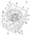
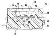
図1及び図2Aは、実施の形態1にかかる半導体装置10の製造過程の途中の様子を図示しており、最終的には、図6に図示するような形態に形成される。このような形態の半導体装置10は、極めて薄型であり、半導体素子28に半導体発光素子を用いた薄型の発光装置として利用されている。
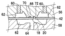
実施の形態1の半導体装置10は、凹部14を備えたハウジング12と、凹部14の底部16に露出した第1リード電極18及び第2リード電極20とを備えている。第1リード電極18は、ダイボンド領域22とワイヤボンド領域24とを有しており、これらの領域は、第1リード電極18の表面に、第1リード電極18を横切って配置された第1壁部26によって区分されている。第2リード電極20は、ダイボンド領域を持たず、ワイヤボンド領域24’のみから構成されている。第1リード電極18と第2リード電極20との間には、第2壁部34が突出している。第1及び第2壁部26、34は、ハウジング12と一体に形成されている。半導体素子28は、その基板側がダイボンド領域22にダイボンド用の接着剤から成る接着層30により固定されており、さらに半導体側に形成された電極がワイヤボンド領域24、24’に導電ワイヤ32により接続されている。
<Embodiment 1>
FIGS. 1 and 2A illustrate a state in the course of the manufacturing process of the
The
第1及び第2壁部26、34は、接着層30を形成する接着剤の接着剤成分がダイボンド領域22からワイヤボンド領域24、24’にブリードせず、また、導電ワイヤ32によるワイヤボンドを阻害しない高さに形成される。壁部26、34は、接着剤成分のブリードを防止でき、そして導電ワイヤのワイヤボンドを妨げなければ、どのような形状にすることもでき、例えば断面矩形、断面三角形、断面台形、断面半円形又は断面半楕円径などの様々な断面形状を有する形態にすることができる。特に、図2Aに示すように、壁部26、34がワイヤボンド領域24、24’からダイボンド領域22に向かって高くなるように傾斜した断面三角形に形成されていると、接着剤成分の堰き止め効果と導電ワイヤ32の張りやすさとに優れているので好ましい。
The first and
図1及び図2A〜2Cに図示するように、第1壁部26は、第1リード電極18の表面上を横切り、両端でハウジング12の側壁38に結合している。実施の形態1では、第1リード電極18の縁部に、第1壁部26を形成する位置に合わせて、矩形の切欠き部36が形成されており、この切欠き部36を介して、第1壁部26とハウジング12の底部40とが強く結合している。このような切欠き部36を形成することにより、第1壁部26と第1リード電極18の表面との密着性が高められて、第1壁部26と第1リード電極18との界面を伝って接着剤成分がブリードするのを、より効果的に抑制できる。
また、第2壁部34は、第1リード電極18と第2リード電極20との間を介してハウジング12の底部40と接続し、また第2壁部34の両端はハウジング12の側壁38に結合している。よって、第1リード電極18と第2リード電極20との間は、第2壁部34によって完全に分離されている。
As shown in FIGS. 1 and 2A to 2C, the
Further, the
図1及び図2Aに図示した半導体装置10では、半導体素子28の配置されたダイボンド領域22が第1及び第2壁部26、34と、ハウジング12の側壁38、38’とによって周囲を囲まれている。このような半導体装置10では、この囲まれたダイボンド領域22内のみに樹脂を滴下すれば、半導体素子28の近傍のみに選択的に樹脂層を形成することができる。例えば、半導体素子28に半導体発光素子を用いたとき、ダイボンド領域22のみに透光性樹脂に蛍光体を含有させたプリコート層を形成すれば、半導体発光素子の近傍のみに蛍光体を配置することができる。
In the
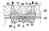
図2B及び図2Cから分かるように、第1リード電極18に切欠き部36を形成することにより、第1壁部26とハウジング12の底部40とを接続する部分が増加している。これにより、第1壁部26の強度が増加し、また第1壁部26を第1リード電極18の表面により密着させることができる。特に、密着性の向上は、接着剤成分が、第1リード電極18と第1壁部26との界面を伝ってワイヤボンド領域24に浸入するのを防止するのに有効である。
また、この切欠き部36は、第1壁部26を形成するときに成形材料の注入を容易にする効果もある。図2Cの矢印f1(図中左側)及び矢印f2(図中右側)は、第1壁部26に成形材料が流れる道筋を示しており、切欠き部36によって、矢印f2の流路は、矢印f1に比べて幅広になっている。第1壁部26は、ワイヤボンドを阻害しない程度に高さが低くて成形材料を充填しにくく、粘度の高い成形材料を使用すると部分的に充填不十分になる恐れがある。しかしながら、切欠き部36を設けることにより充填流路が広がり、成形材料を充填しやすくなる。このように、実施の形態1は、第2リード電極20に比べて形成しにくい第1リード電極18を設けるにあたり、第1リード電極18が切欠き部36を有することにより、第1リード電極18が形成しやすくなる点でも有利である。
また、実施の形態1では、幅の狭い第1リード電極18を備えた半導体装置であるので、第1リード電極18の縁部の一部を切欠いた切欠き部36として、第1リード電極18の強度を維持するのが好ましい。
As can be seen from FIGS. 2B and 2C, by forming the
The
In the first embodiment, since the semiconductor device includes the
切欠き部36は、図2A及び図2Bでは第1リード電極18の縁部を長方形に切り抜いて形成されているが、切欠き部36の形状はこれに限定されるものではなく、例えば、正方形、台形等の矩形、三角形や五角形等の多角形、半円形、又は半楕円形など、さまざまな形状に切り抜いて形成することができる。また、図示した切欠き部36は、第1壁部26に完全に隠れる寸法にされているが、第1壁部26から一部露出しても構わない。さらに、第1リード電極18の厚さ方向に向かって寸法が変わる、いわゆる漏斗状になっていてもよく、特に、ハウジング12の底部40側から凹部14側に向かって寸法が小さくなっていると、成形材料の注入に有利になり、また第1リード電極18の強度を維持できるので好ましい。
2A and 2B, the
本発明の半導体装置10は、ハウジング12の凹部14に樹脂を充填して、凹部14内に固定した半導体素子28を外部環境から保護するのが好ましい。特に、半導体素子28が半導体発光素子の場合には、充填する樹脂に透光性樹脂を選択すれば、光を取り出すことができる。また、半導体発光素子28の発光色とは異なる色を発光させたい場合には、透光性樹脂に蛍光体を混ぜることにより発光波長を変換することができる。
In the
以下に、本発明の半導体装置10の製造方法を、1.ハウジング12を製造する工程と、2.ハウジング12から半導体装置10を製造する工程とに分けて説明する。
Hereinafter, a method for manufacturing the
(1.ハウジング12の製造)
図3を参照しながら、ハウジング12の製造工程を説明する。
まず、金属平板に打ち抜き加工を施して、その表面に金属メッキを施してリードフレーム42を作製する。リードフレーム42には、第1リード電極18及び第2リード電極20から成る一対のリード電極が形成されている。第1リード電極18と第2リード電極20とは、隙間をあけて対向している。通常は、1枚の金属平板に、多数のリード電極18、20の対を形成する。
(1. Production of housing 12)
The manufacturing process of the
First, a metal plate is punched, and the surface is plated with metal to produce the
次に、図3Aに示すように、リードフレーム42を上下に分割されたハウジング成型用のモールド金型56、58の間に配置して、上下のモールド金型56、58で挟み込む。このとき、一対のリード電極18、20と、リードフレーム42のハンガーリード46とが、ハウジング12の形状を有するモールド金型56、58の空洞62の中に位置するように位置決めして、モールド金型56、58で挟み込む。ハンガーリード46とは、リードフレーム32に固定されたハウジング12の姿勢を保つための部材であり、リードフレーム42の抜き打ち加工のときに形成される。図1にも図示されているように、ハンガーリード46の先端部分は、リードフレーム32からハウジング12を分離するまで、ハウジング12の側面に食い込んだ状態になる。
上側モールド金型56には、ハウジング12の凹部14の形状に一致した突出部66を備えている。この突出部66には、壁部26、34の外形に一致した溝70、72が形成されている。
Next, as shown in FIG. 3A, the
The
その後、図3Bのように、下側モールド金型58の材料注入ゲート64から、モールド金型56、58の空洞62内に成形材料68を注入する。上側モールド金型56には、ハウジング12の凹部14に対応する突出部66が形成されており、この突出部66がリード電極18、20の上面に接触した状態で成形材料68を注入すれば、リード電極18の上面には成形材料68が付着せず、得られたハウジング12の凹部14の底面にリード電極18、20を露出させることができる。
この例では、ハウジング12の凹部14の底面には、リード電極18が完全に露出しているが、必ずしも完全に露出している必要はない。例えば、凹部14の底面の直下にリード電極18、20を位置させる(すなわち、リード電極18、20はハウジングの成形材料によって覆われている)と共に、凹部の底面に穴等をあけることにより、凹部内にリード電極の一部を露出させるようにしてもよい。この穴等を介して、半導体素子とリード電極とを導通すれば、本発明の半導体装置を形成することができる。
Thereafter, as shown in FIG. 3B, the
In this example, the
成形材料68は、溝70、72に注入されて、それぞれ第1壁部26及び第2壁部34を形成する。溝72には、第1リード電極18と第2リード電極20との隙間から成形材料68が注入できるので、成形材料68の充填が容易である。これに対して溝70は、成形材料68が注入しにくい。図2Cを参照して説明すると、溝70に充填するには、第1リード電極18と、ハウジング12の外壁面を成型する金型の内壁面と、の間に形成された狭い隙間を通じて、成形材料68を矢印f1のように注入するしかない。しかしながら、実施の形態1に示すように、第1リード電極18に切欠き部36を設けることにより、成形材料68は、矢印f2のように切欠き部36を介して溝部72に充填できるので、成形材料68が注入しやすい。このように、第1リード電極18が、第1壁部26の直下の位置に切欠き部36を有すると、溝70に成形材料68が充填しやすくなり、第1壁部26が充填不十分で一部欠如する等の欠陥が生じにくくなる。
The
図3Cのように、モールド金型56、58内の空洞62及び溝部70、72に十分な量の成形材料68が充填されたら、成形材料68の充填を停止し、成形材料68を硬化させる。
成形材料68が完全に硬化したら、図3Dに示すように、まず下側モールド金型58を外し、次いで上側モールド金型56を外してハウジング12を取り出す。ここで、上側モールド金型56を外す際には、リードフレーム42が歪んだり、ハウジング12が傾いたりする不具合を生じやすい。そこで、例えば、上側モールド金型56にスライド可能に挿通してある押出しピン60を矢印方向に押し出せば、そのような不具合を起こさずにハウジング12を取り出すことができる。
As shown in FIG. 3C, when a sufficient amount of the
When the
図3に示す一連の工程により、図1及び図4に示すようなハウジング12が一部に成型されたリードフレーム42が得られる。
図1に示すように、リードフレーム42に固定されたハウジング12は、凹部14の内部に露出した第1リード電極18及び第2リード電極を備えており、それぞれのリード電極18、20が、リードフレーム42に接続した第1外部電極78及び第2外部電極80と繋がっている。また、ハウジング12の側面には、ハンガーリード46の先端が食い込んでいる。ハウジング12は、外部電極78、80とハンガーリード46とによってリードフレーム42に係持されている。
The
As shown in FIG. 1, the
なお、図1及び図4では、ハウジング12が1つだけ形成されているが、通常は、図5に示すように1枚のリードフレーム42に多数(この図では縦3個×横2個の計6個)のハウジング12、12・・・が形成される。多数のハウジング12、12・・・を製造する場合には、多数のハウジング用空洞62を有するモールド金型56、58を使用して、それらの空洞62に同時に成形材料を注入することにより、全てのハウジング12、12・・・を同時に形成することができる。
1 and 4, only one
(2.半導体装置10の製造工程)
次いで、図1及び図4を参照しながら、ハウジング12に半導体素子28を実装して半導体装置を製造する工程を説明する。
ハウジング12の凹部14内で、第1リード電極18のダイボンド領域22に、半導体素子28をダイボンドし、さらに、半導体素子28の電極(正極及び負極)と、第1リード電極18のワイヤボンド領域24及びリード電極20(ワイヤボンド領域24’でもある)とのそれぞれを、導電ワイヤ32によってワイヤボンドする。
(2. Manufacturing process of semiconductor device 10)
Next, a process of manufacturing a semiconductor device by mounting the
Within the
ダイボンドで使用される接着剤は、目的に合わせて選択される。例えば、使用する接着剤の表面張力が低い場合、接着剤成分がダイボンド領域22全体に広がって、ダイボンド領域22の表面を覆うことがある。しかしながら、ダイボンド領域22とワイヤボンド領域24、24’との間に第1及び第2壁部26、34、が形成されているので、接着剤成分がワイヤボンド領域24、24’にまで広がることがない。よって、ダイボンドの後にワイヤボンドをする際に、接着剤成分がワイヤボンドの障害になることがない。
また、壁部26、34の高さは、ワイヤボンドの障害にならない程度の高さにしているので、従来どおりのワイヤボンダを用いてワイヤボンドすることができ、また導電ワイヤ32の長さを必要以上に長くせずにすむので、ワイヤボンドにかかるコストを従来と同等にすることができる。
The adhesive used in die bonding is selected according to the purpose. For example, when the surface tension of the adhesive to be used is low, the adhesive component may spread over the entire
Moreover, since the height of the
その後に、ハウジング12の凹部14を樹脂44で充填して、半導体素子28及び導電ワイヤ32を封止する。樹脂44は、ハウジング12の凹部14内にポッティング等によって充填された後に硬化させる。
ここで、半導体発光素子に青色発光ダイオードを、樹脂44に透光性樹脂を使用し、さらに透光性樹脂に青色光を吸収して黄色光を発する蛍光体を分散させることにより、薄型の白色発光装置を得ることができる。この薄型の白色発光装置を導光板と組み合わせることにより、バックライトに適した光源を得ることができる。
Thereafter, the
Here, a blue light-emitting diode is used for the semiconductor light-emitting element, a light-transmitting resin is used for the
樹脂44の封止が完了すると、外部電極78、80は、破線Xの位置で切断してリードフレーム42から分離する。外部電極78、80は、ハウジング12の外形に沿って折り曲げて、図6に図示するようなJ−ベンド(Bend)型の形状に成形される(外部電極78、80のカットフォーミングと呼ばれる)。このとき、ハウジング12は、ハンガーリード46のみでリードフレーム42に支持されているが、カットフォーミングの際にかかる応力でハウジング12が傾いてリードフレーム42から脱落しないように、ハウジング12を保持する治具を利用するのが好ましい。
このカットフォーミングは、1枚のリードフレーム42に形成された複数のハウジング12に対して同時に行えるので、発光装置10の製造効率を向上させることができる。
When the sealing of the
Since this cut forming can be performed simultaneously on the plurality of
図6の半導体装置10を製造する場合、カットフォーミングの最初に、外部電極78、80の狭幅部分をハウジング12の凹部14方向に折り曲げ、その後に外部電極87、80の広幅部分でハウジング12の外形からはみ出た部分をJ−ベント型に折り曲げる。これ以外のカットフォーミングとして、外部電極78、80の狭幅部分を、ハウジング12の凹部14と反対方向に折り曲げた形態や、J―ベント型に折り曲げない形態など、用途に合わせて変形が可能である。
When the
カットフォーミングか完了したら、最後に、ハウジング12をリードフレーム42から外す。ハンガーリード46、46’を折り曲げることにより、ハンガーリード46の先端をハウジング12から簡単に外すことができる。
When the cut forming is completed, finally, the
<実施の形態2>
実施の形態2にかかる半導体装置は、図7A及び図7Bに示すように、第1リード電極18の表面にV字溝50が形成されている。V字溝50は、第1壁部26の直下に位置している。実施の形態2の半導体装置10は、第1リード電極18及び第1壁部26を除いては、実施の形態1と同様である。
<Embodiment 2>
In the semiconductor device according to the second embodiment, as shown in FIGS. 7A and 7B, a V-shaped
図7A〜7Cに図示するように、第1壁部26は、第1リード電極18の表面上を横切り、両端でハウジング12の側壁38に結合している。実施の形態2では、第1リード電極18の表面に、V字溝50が形成されていて、そのV字溝50の上に、第1壁部26が形成されている。このV字溝50は、ダイボンド領域22とワイヤボンド領域24との間を区分する第1壁部26に沿って形成されるのが好ましい。すなわち、V字溝50は、第1壁部26と共に、第1リード電極18の表面をダイボンド領域22とワイヤボンド領域24とを区分している。このようなV字溝50があると、ダイボンド用の接着剤の接着剤成分が第1リード電極18と第1壁部26との界面を伝ってワイヤボンド領域24方向に浸入してきても、V字溝50の窪みに溜まってそれ以上浸入できなくなる。すなわち、第1壁部26の直下にV字溝50を備えることによって、接着剤成分がワイヤボンド領域24に浸入するのを確実に防止することができる。
As shown in FIGS. 7A to 7C, the
また、第1壁部26の断面積がV字溝50の分だけ大きくなることにより、第1壁部26の強度が増加する。さらに、第1壁部26の断面積の増加は、壁部26とハウジング12の側壁38との結合強度も増加する。結合強度の増加により、第1壁部26と第1リード電極18の表面との密着性が高まり、これにより、接着剤成分が第1リード電極18と第1壁部26との界面を伝ってワイヤボンド領域24に浸入するのを抑制するのに有効である。
In addition, since the cross-sectional area of the
このV字溝50は、第1壁部26の形成時にも有利である。図3Bに相当する工程において成形材料68をモールド金型56、58に注入するときにも、有利な効果を奏する。即ち、図7Cに示すように、上側のモールド金型56の溝70に成形材料68を注入して第1壁部26を形成するとき、V字溝50が形成されていなければ、成形材料68は矢印f1及びf2のように狭い部分から注入される。これに対して、V字溝50を形成したときは、矢印f3及びf4のように広い間口から注入でき、充填しやすくなる。このように、第1リード電極18が、第1壁部26の直下の位置にV字溝50を有すると、溝70に成形材料68が充填しやすくなり、第1壁部26が充填不十分で一部欠如する等の欠陥が生じにくくなる。このように、実施の形態2は、第2リード電極20に比べて形成しにくい第1リード電極18を設けるにあたり、第1リード電極18がV字溝50を有することにより、第1リード電極18が形成しやすくなる点でも有利である。
The V-shaped
第1リード電極18の表面に形成したV字溝50は、別の断面形状の溝に置き換えることができる。例えば、正方形、台形等の矩形、三角形や五角形等の多角形、半円形、又は半楕円形など、さまざまな断面形状の溝を形成することができる。特に、断面V字状のV字溝50は、簡単な器具を押圧して成形でき、接着剤成分の浸入防止効果も高いので好ましい。
The V-shaped
また、図7Aに図示した半導体装置10では、半導体素子28の配置されたダイボンド領域22が第1壁部26及び第2壁部34と、ハウジング12の側壁38とによって周囲を囲まれている。このような半導体装置10では、この囲まれたダイボンド領域22内のみに樹脂を滴下すれば、半導体素子28の近傍のみに選択的に樹脂層を形成することができる。例えば、半導体素子28に半導体発光素子を用いたとき、ダイボンド領域22のみに透光性樹脂に蛍光体を含有させたプリコート層を形成すれば、半導体発光素子の近傍のみに蛍光体を配置することができる。
In the
<実施の形態3>
実施の形態1では、切欠き部36を形成し、実施の形態2では、V字溝50を形成している。実施の形態3にかかる半導体装置は、図8A〜図8Bに示すように、第1リード電極18に、切欠き部36とV字溝50とが共に形成されている。それ以外は、実施の形態1及び2と同様である。なお、切欠き部36及びV字溝50の詳細な形態についても、以下に説明する以外については実施の形態1及び2と同様である。
<Embodiment 3>
In the first embodiment, the
図8A〜8Cに図示するように、第1壁部26は、第1リード電極18の表面上を横切り、両端でハウジング12の側壁38に結合している。
実施の形態3では、第1リード電極18の縁部181に、第1壁部26を形成する位置に合わせて、矩形の切欠き部36が形成されている。これにより、実施の形態1の切欠き部36と同様に、第1壁部26と第1リード電極18の表面との密着性が高められて、第1壁部26と第1リード電極18との界面を伝って接着剤成分がブリードするのを抑制する効果が得られる。
As shown in FIGS. 8A to 8C, the
In the third embodiment, a
また、実施の形態3では、第1リード電極18の表面にV字溝50が形成されていて、そのV字溝50の上に、第1壁部26が形成されている。このV字溝50は、ダイボンド領域22とワイヤボンド領域24との間を区分する第1壁部26に沿って形成されるのが好ましい。すなわち、V字溝50は、第1壁部26と共に、第1リード電極18の表面をダイボンド領域22とワイヤボンド領域24とを区分している。これにより、実施の形態2のV字溝50と同様に、第1壁部26の直下にV字溝50を備えることによって、接着剤成分がワイヤボンド領域24に浸入するのを確実に防止できる効果が得られる。
In the third embodiment, the V-shaped
そして、実施の形態3では、V字溝50の一端501が切欠き部36と接続していることから、図3Bに相当する工程において成形材料68をモールド金型56、58に注入するときに、極めて有利な効果を奏する。
まず、図8Cの矢印f1(図中左側)及び矢印f2及びf4(図中右側)は、第1壁部26を形成するためのモールド金型56の溝70に、成形材料68が流れる道筋を示している。切欠き部36によって、矢印f2及びf4の流路は、矢印f1に比べて幅広になっていることがわかる。第1壁部26は、ワイヤボンドを阻害しない程度に高さを低くされているので、それに合わせて溝70の空間も狭い。よって、溝70には成形材料を充填しにくく、粘度の高い成形材料を使用すると部分的に充填不十分になる恐れがある。しかしながら、切欠き部36を設けることにより充填流路が広がり、成形材料68を充填しやすくなる。
そして、矢印f2及びf4の流路を通った成形材料68は、V字溝50によって広くなった間口から溝70の内部に向かって流れ込むので、V字溝50のない場合に比べて充填しやすい。
In the third embodiment, since one
First, an arrow f 1 (left side in the figure) and arrows f 2 and f 4 (right side in the figure) in FIG. 8C indicate that the
Then, the
このように、切欠き部36とV字溝50とを設け、且つ切欠き部36とV字溝50とを接続することにより、実施の形態1及び2と比べても、第1壁部26の充填がさらに容易になる利点がある。
その反面、第1リード電極18うち、第1壁部26直下に位置する部分は、切欠き部36によって狭幅にされ且つV字溝50によって肉薄にされているので、他の部分に比べて強度が低くなる問題が発生する。もし製造途中で第1リード電極18の先端に応力がかかれば、V字溝50に沿って屈曲するおそれや、さらには切断する危険性もある。
そこで、実施の形態3では、V字溝50の他端502を第1リード電極の縁部182より手前で終端させることにより、第1リード電極18が極度に強度低下するのを抑制している。ただし、V字溝50の他端502が第1リード電極の縁部182まで達しているほうが、成形材料68の充填の観点では有利なので、第1リード電極18の強度が十分で、屈曲や切断のおそれが少ない場合には、他端502を端部182まで延長するのが好ましい。
Thus, by providing the
On the other hand, the portion of the
Therefore, in the third embodiment, the
<実施の形態4>
図9A〜図9Cは、実施の形態3にかかる半導体装置10であり、凹部14を備えたハウジング12と、凹部14の底部16に露出した第1リード電極18及び第2リード電極20とを備えている。第1リード電極18は、ダイボンド領域22とワイヤボンド領域24とを有しており、これらの領域は、第1リード電極18の表面に、第1リード電極18を横切って配置された第1壁部26によって区分されている。第2リード電極20は、ダイボンド領域を持たず、ワイヤボンド領域24’のみから構成されている。第1リード電極18と第2リード電極20との間には、第2壁部34が突出している。第1及び第2壁部26、34は、ハウジング12と一体に形成されている。半導体素子28は、その基板側がダイボンド領域22にダイボンド用の接着剤から成る接着層30により固定されており、さらに半導体側に形成された電極がワイヤボンド領域24、24’に導電ワイヤ32、32’により接続されている。また、この半導体装置10は、半導体素子28に過剰な電流が通電されるのを保護する保護素子52を備えており、この保護素子も、ダイボンド領域22に接着剤でダイボンドされている。
<Embodiment 4>
9A to 9C show a
実施の形態4では、第1壁部26と第2壁部34とが繋がって、一体に形成されている。第1及び第2壁部26、34は、接着剤成分がダイボンド領域22からワイヤボンド領域24、24’にブリードせず、また、導電ワイヤ32、32’によるワイヤボンドを阻害しない高さに形成される。壁部26、34は、接着剤成分のブリードを防止でき、そして導電ワイヤのワイヤボンドを妨げなければ、どのような形状にすることもでき、図9A〜図9Cのように断面矩形以外にも、例えば断面三角形、断面台形、断面半円形又は断面半楕円径などの様々な断面形状を有する形態にすることができる。
In Embodiment 4, the
図9A〜9Cに図示するように、第1壁部26は、第1リード電極18の表面上を横切り、そのままハウジング12の側壁38まで伸びている。実施の形態4では、第1リード電極18に円形の貫通孔36’が形成されており、この貫通孔36’を介して、第1壁部26とハウジング12の底部40とが強く結合している。このような貫通孔36’ を形成することにより、第1壁部26と第1リード電極18の表面との密着性が高められて、第1壁部26と第1リード電極18との界面を伝ってボンディング樹脂がブリードするのを、より効果的に抑制できる。
また、第2壁部34は、第1リード電極18と第2リード電極20との間を介してハウジング12の底部40と接続し、また第2壁部34の両端もハウジング12の側壁38まで伸びている。よって、ハウジングの凹部内の第1リード電極18と第2リード電極20との間は、第2壁部34によって完全に分離されている。
As illustrated in FIGS. 9A to 9C, the
The
第1リード電極18には、第1壁部26を形成する位置に合わせて、貫通孔36’が形成されている。図9A〜図9Cから分かるように、貫通孔36’を形成することにより、第1壁部26の中央付近が、ハウジング12の底部40に接続される。これにより、第1壁部26の強度が増加し、また第1壁部26を第1リード電極18の表面により密着させることができる。また、密着性の向上は、接着剤成分が、第1リード電極18と第1壁部26との界面を伝ってワイヤボンド領域24に浸入するのを防止するのに有効である。また、この切欠き部36は、第1壁部26を形成するときに成形材料の注入を容易にして、第1壁部26が充填不十分で一部欠如する等の欠陥が生じにくくする効果がある。
A through
また、実施の形態4では、幅の広い第1リード電極18を備えた半導体装置であるので、第1リード電極18を貫通する穴部から成る貫通孔36’を形成しても、第1リード電極18の強度を維持することができる。幅の広い第1リード電極18では、実施の形態1のような縁部に形成した切欠き部36よりは、第1リード電極18の縁部以外に貫通孔として形成した貫通孔36’のほうが好ましく、第1壁部26とハウジング12の底部40との結合により第1リード電極18が浮き上がるのを抑える、いわゆるアンカーホールとしても機能する。
In the fourth embodiment, since the semiconductor device includes the wide first
貫通孔36’は、図9A〜図9Cでは円形に長方形に切り抜かれているが、これに限定されるものではなく、例えば、正方形、長方形、台形等の矩形、三角形や五角形等の多角形、又は楕円形など、さまざまな形状に切り抜いて形成することができる。また、図示した貫通孔36’の直径は、第1壁部26の幅以上に大きくされているのが好ましい。これは以下の理由による。
第1壁部26を形成するためのモールド金型56の溝70に成形材料68を充填するとき、貫通孔36’から注入される成形材料68は、溝70の長さ方向には比較的流れやすいが、幅方向には流れにくい。そして、その流れやすさの傾向は、溝70の高さが小さくなると、より顕著になる。本発明では、第1壁部26を、導電ワイヤ32のワイヤボンディングを阻害しない程度の低さにしているので、貫通孔36’から流入した成形材料68は、溝70の幅方向に極めて流れにくくなる。その結果、貫通孔36’の近傍の、特に第1壁部26の幅方向において、成形材料68の未充填による欠陥ができるおそれがある。これに対して、貫通孔36’の直径を第1壁部26の幅よりも大きくすれば、貫通孔36’から注入した成形材料68は、初めから第1壁部26の幅いっぱいに充填されるので、成形材料68の未充填の問題が発生しない。
ただし、成形材料68の回り込みが良好で、溝70全体に成形材料8を十分に充填できる場合には、貫通孔36’の直径を、第1壁部26の幅よりも小さくしても問題はない。
9A to 9C, the through hole 36 'is cut into a circle and a rectangle. However, the through hole 36' is not limited to this. Or it can cut out and shape in various shapes, such as an ellipse. In addition, the diameter of the illustrated through
When the
However, if the
また、実施の形態2のように、第1リード電極18の表面にV字溝50を形成することもできる。V字溝は、第1壁部26の直下で、且つ第1壁部26に沿って形成するのが好ましい。V字溝を形成することにより、ダイボンド用の接着剤の接着剤成分が第1リード電極18と第1壁部26との界面を伝ってワイヤボンド領域24方向に浸入してきても、V字溝の窪みに溜まってそれ以上浸入できなくなる。
そして、V字溝は、第1壁部26を形成するときに、成形材料がV字溝を通って第1壁部26に注入されるので、十分に充填することが可能になる。よって、体積が小さく、注入口も狭いため、成形材料を充填しにくい第1壁部26であっても、充填不十分により一部欠如する等の欠陥が生じにくくなる。
Further, as in the second embodiment, a V-shaped
The V-shaped groove can be sufficiently filled because the molding material is injected into the
本発明の半導体装置10は、ハウジング12の凹部14に樹脂を充填して、凹部14内に固定した半導体素子28を外部環境から保護するのが好ましい。特に、半導体素子28が半導体発光素子の場合には、充填する樹脂に透光性樹脂を選択すれば、光を取り出すことができる。また、半導体発光素子28の発光色とは異なる色を発光させたい場合には、透光性樹脂に蛍光体を混ぜることにより発光波長を変換することができる。
In the
実施の形態4にかかる半導体装置10は、実施の形態1の半導体装置10とは形状が大きく異なっているが、適切なリードフレームとモールド金型とを使用することにより、同様の製造方法によって成形することができる。
The
<好適な材料>
実施の形態1〜4の半導体装置10の各構成部材に適した材料ついて、以下に詳述する。
(第1及び第2リード電極18、20、第1及び第2外部電極78、80)
第1リード電極18、第2リード電極20、第1外部電極78及び第2外部電極80は、すべて同一の導電性材料から形成されており、加工性や強度の観点からすると、鉄、銅、鉄入り銅、錫入り銅及び銅、金、銀をメッキしたアルミニウム、鉄、銅等から形成するのが好ましい。
<Suitable material>
Materials suitable for the respective constituent members of the
(First and second
The
(ハウジング12及び壁部26、34)
ハウジング12及び壁部26、34の成形材料には、例えば、液晶ポリマー、ポリフタルアミド樹脂、ポリブチレンテレフタレート(PBT)などの熱可塑性樹脂を用いることができる。特に、ポリフタルアミド樹脂のような高融点結晶を含有する半結晶性ポリマー樹脂は、表面エネルギーが大きく、ハウジング12の凹部14に充填する封止樹脂との密着性が良好であるので、好適である。これにより、封止樹脂を充填し硬化する工程において、樹脂の冷却過程の間にハウジングと封止樹脂との界面が剥離しにくくなる。また、半導体素子28に半導体発光素子を用いて半導体発光装置10を製造するならば、成形材料中に酸化チタンなどの白色顔料などを混合して、ハウジング12の反射率を高めることもできる。
(
For the molding material of the
(接着層30)
接着層30は、ダイボンド用の接着剤から形成されており、エポキシ樹脂、シリコーン樹脂などの絶縁性接着剤や、銀ペーストなどの導電性接着剤を使用することができる。
本発明では、壁部を備えているので、従来は使用しにくかったエポキシ樹脂のような表面張力の低い接着剤成分を含む接着剤も使用できる。
(Adhesive layer 30)
The
In the present invention, since the wall portion is provided, an adhesive containing an adhesive component having a low surface tension such as an epoxy resin, which has been difficult to use conventionally, can be used.
(導電ワイヤ32)
ワイヤボンディング用の導電ワイヤ32としては、例えば、金線、銅線、白金線、アルミニウム線等の金属及びそれらの合金から成る金属製のワイヤを用いることが出来る。
(Conductive wire 32)
As the
(樹脂44)
凹部14を封止するのに樹脂44に適した材料としては、例えば、シリコーン樹脂、エポキシ樹脂、ユリア樹脂、フッ素樹脂、及び、それらの樹脂を少なくとも一種以上含むハイブリッド樹脂等の耐候性に優れた樹脂が挙げられる。また、樹脂44に代えて、ガラス、シリカゲルなどの耐光性に優れた無機物を用いることもできる。これらの樹脂や無機物は、透光性にすることができるので、半導体発光装置10を製造する場合にも適している。
また、白色の半導体発光装置10を製造する場合には、半導体素子28に青色発光ダイオードを用い、透光性の樹脂44に蛍光体の粒子を分散させるとよい。蛍光体としては、青色光を吸収して黄色光を発する希土類系蛍光体(例えばYAG系蛍光体)が好適である。
(Resin 44)
Examples of a material suitable for the
When manufacturing the white semiconductor
10 半導体発光装置、 12 ハウジング、 14 凹部、 18 第1リード電極、 20 第2リード電極、 22 ダイボンド領域、 24、24’ ワイヤボンド領域、 26 第1壁部、 28 半導体素子、 30 接着層、 32 導電ワイヤ、 34 第2壁部、 36 切欠き部、 36’ 貫通孔、 42 リードフレーム、 50 V字溝、 52 保護素子、 78 第1外部電極、 80 第2外部電極、 181、182 第1リード電極の縁部、 501 V字溝の一端、 502 V字溝の他端。
DESCRIPTION OF
Claims (10)
前記半導体素子を収納する凹部を備えたハウジングと、
前記凹部の底面に露出した第1リード電極及び第2リード電極と、
前記半導体素子を前記第1リード電極にダイボンドする接着層と、
前記半導体素子の前記一対の電極と、前記第1リード電極及び前記第2リード電極とをそれぞれワイヤボンドする導電ワイヤと、を備えた半導体装置であって、
前記ハウジングが、前記凹部の前記底面に、前記第1リード電極の表面をダイボンド領域とワイヤボンド領域とに区分するように横断して設けられた少なくとも1つの第1壁部を備えており、
前記第1リード電極は、少なくとも前記第1壁部の直下に、前記第1リード電極の縁部を切り欠いた切欠き部を備えており、前記第1壁部と前記ハウジングの底部とが、前記切欠き部を通じて接続されており、
前記第1壁部の断面が前記ワイヤボンド領域から前記ダイボンド領域に向かって高くなるように傾斜されていることを特徴とする半導体装置。 A semiconductor element having a pair of electrodes;
A housing having a recess for housing the semiconductor element;
A first lead electrode and a second lead electrode exposed on the bottom surface of the recess;
An adhesive layer for die-bonding the semiconductor element to the first lead electrode;
A semiconductor device comprising: the pair of electrodes of the semiconductor element; and a conductive wire that wire-bonds the first lead electrode and the second lead electrode, respectively.
The housing includes at least one first wall provided on the bottom surface of the recess so as to traverse the surface of the first lead electrode into a die bond region and a wire bond region;
The first lead electrode includes a cutout portion formed by cutting out an edge portion of the first lead electrode at least immediately below the first wall portion, and the first wall portion and the bottom portion of the housing are provided. Connected through the notch ,
The semiconductor device, wherein the cross section of the first wall portion is inclined so as to become higher from the wire bond region toward the die bond region .
前記半導体素子を収納する凹部を備えたハウジングと、
前記凹部の底面に露出した第1リード電極及び第2リード電極と、
前記半導体素子を前記第1リード電極にダイボンドする接着層と、
前記半導体素子の前記一対の電極と、前記第1リード電極及び前記第2リード電極とをそれぞれワイヤボンドする導電ワイヤと、を備えた半導体装置であって、
前記ハウジングが、前記凹部の前記底面に、前記第1リード電極の表面をダイボンド領域とワイヤボンド領域とに区分するように横断して設けられた少なくとも1つの第1壁部を備えており、
前記第1リード電極は、少なくとも前記第1壁部の直下に、前記第1リード電極の縁部を切り欠いた切欠き部を備えており、前記第1壁部と前記ハウジングの底部とが、前記切欠き部を通じて接続されており、
前記ハウジングが、前記凹部の前記底面に、前記第1リード電極と前記第2リード電極との間を介して前記ハウジングの前記底部と接続する第2壁部を有し、
前記ダイボンド領域が、前記第1壁部、前記第2壁部および前記ハウジングの側壁によって包囲されていることを特徴とする半導体装置。 A semiconductor element having a pair of electrodes;
A housing having a recess for housing the semiconductor element;
A first lead electrode and a second lead electrode exposed on the bottom surface of the recess;
An adhesive layer for die-bonding the semiconductor element to the first lead electrode;
A semiconductor device comprising: the pair of electrodes of the semiconductor element; and a conductive wire that wire-bonds the first lead electrode and the second lead electrode, respectively.
The housing includes at least one first wall provided on the bottom surface of the recess so as to traverse the surface of the first lead electrode into a die bond region and a wire bond region;
The first lead electrode includes a cutout portion formed by cutting out an edge portion of the first lead electrode at least immediately below the first wall portion, and the first wall portion and the bottom portion of the housing are provided. Connected through the notch,
The housing has a second wall portion connected to the bottom portion of the housing through the space between the first lead electrode and the second lead electrode on the bottom surface of the recess;
The semiconductor device in which the die bonding area, and the first wall portion, characterized in that it is surrounded by the second wall portion and side wall of the housing.
前記半導体素子を収納する凹部を備えたハウジングと、
前記凹部の底面に露出した第1リード電極及び第2リード電極と、
前記半導体素子を前記第1リード電極にダイボンドする接着層と、
前記半導体素子の前記一対の電極と、前記第1リード電極及び前記第2リード電極とをそれぞれワイヤボンドする導電ワイヤと、を備えた半導体装置であって、
前記ハウジングが、前記凹部の前記底面に、前記第1リード電極の表面をダイボンド領域とワイヤボンド領域とに区分するように横断して設けられた少なくとも1つの第1壁部を備えており、
前記第1リード電極は、少なくとも前記第1壁部の直下に、前記第1リード電極の縁部を切り欠いた切欠き部を備えており、前記第1壁部と前記ハウジングの底部とが、前記切欠き部を通じて接続されており、
前記切欠き部は、前記ハウジングの前記底部から前記凹部に向かって寸法が小さくなる漏斗状であることを特徴とする半導体装置。 A semiconductor element having a pair of electrodes;
A housing having a recess for housing the semiconductor element;
A first lead electrode and a second lead electrode exposed on the bottom surface of the recess;
An adhesive layer for die-bonding the semiconductor element to the first lead electrode;
A semiconductor device comprising: the pair of electrodes of the semiconductor element; and a conductive wire that wire-bonds the first lead electrode and the second lead electrode, respectively.
The housing includes at least one first wall provided on the bottom surface of the recess so as to traverse the surface of the first lead electrode into a die bond region and a wire bond region;
The first lead electrode includes a cutout portion formed by cutting out an edge portion of the first lead electrode at least immediately below the first wall portion, and the first wall portion and the bottom portion of the housing are provided. Connected through the notch,
The notch portion is a semiconductor device characterized in that from the bottom of the housing is a funnel-shape dimension becomes smaller toward the recess.
前記半導体素子を収納する凹部を備えたハウジングと、
前記凹部の底面に露出した第1リード電極及び第2リード電極と、
前記半導体素子を前記第1リード電極にダイボンドする接着層と、
前記半導体素子の前記一対の電極と、前記第1リード電極及び前記第2リード電極とをそれぞれワイヤボンドする導電ワイヤと、を備えた半導体装置であって、
前記ハウジングが、前記凹部の前記底面に、前記第1リード電極の表面をダイボンド領域とワイヤボンド領域とに区分するように横断して設けられた少なくとも1つの第1壁部を備えており、
前記第1リード電極は、少なくとも前記第1壁部の直下に、前記第1リード電極に形成された貫通孔を備えており、前記第1壁部と前記ハウジングの底部とが、前記貫通孔を通じて接続されていることを特徴とする半導体装置。 A semiconductor element having a pair of electrodes;
A housing having a recess for housing the semiconductor element;
A first lead electrode and a second lead electrode exposed on the bottom surface of the recess;
An adhesive layer for die-bonding the semiconductor element to the first lead electrode;
A semiconductor device comprising: the pair of electrodes of the semiconductor element; and a conductive wire that wire-bonds the first lead electrode and the second lead electrode, respectively.
The housing includes at least one first wall provided on the bottom surface of the recess so as to traverse the surface of the first lead electrode into a die bond region and a wire bond region;
The first lead electrode includes a through hole formed in the first lead electrode at least immediately below the first wall portion, and the first wall portion and the bottom portion of the housing pass through the through hole. A semiconductor device which is connected.
前記第1壁部および前記第2壁部によって包囲された領域に、前記半導体素子と、当該半導体素子を保護する保護素子とが配置されている請求項4又は5に記載の半導体装置。 The housing has a plurality of second wall portions connected to the bottom portion of the housing through the space between the first lead electrode and the second lead electrode on the bottom surface of the recess;
Wherein the enclosed region by the first wall portion and the second wall portion, wherein the semiconductor device, the semiconductor device according to claim 4 or 5 and a protection element to protect the semiconductor element is arranged.
前記溝部は前記第1壁部に沿って延在すると共に、前記溝部に前記第1壁部の底部が係合している請求項1乃至6のいずれか1項に記載の半導体装置。 On the surface of the first lead electrode, a groove is further provided immediately below the first wall,
Wherein with groove extending along said first wall portion, the semiconductor device according to any one of claims 1 to 6 the bottom of the first wall portion is engaged with the groove.
前記半導体素子を収納する凹部を備えたハウジングと、
前記凹部の底面に露出した第1リード電極及び第2リード電極と、
前記半導体素子を前記第1リード電極にダイボンドする接着層と、
前記半導体素子の前記一対の電極と、前記第1リード電極及び前記第2リード電極とをそれぞれワイヤボンドする導電ワイヤと、を備えた半導体装置であって、
前記ハウジングが、前記凹部の前記底面に、前記第1リード電極の表面をダイボンド領域とワイヤボンド領域とに区分するように横断して設けられた少なくとも1つの壁部を備えており、
前記第1リード電極の表面には、前記壁部の直下に溝部が設けられており、前記溝部は前記壁部に沿って延在すると共に、前記溝部に前記壁部の底部が係合していることを特徴とする半導体装置。 A semiconductor element having a pair of electrodes;
A housing having a recess for housing the semiconductor element;
A first lead electrode and a second lead electrode exposed on the bottom surface of the recess;
An adhesive layer for die-bonding the semiconductor element to the first lead electrode;
A semiconductor device comprising: the pair of electrodes of the semiconductor element; and a conductive wire that wire-bonds the first lead electrode and the second lead electrode, respectively.
The housing includes at least one wall portion provided on the bottom surface of the recess so as to traverse the surface of the first lead electrode into a die bond region and a wire bond region;
On the surface of the first lead electrode, a groove is provided immediately below the wall. The groove extends along the wall, and the bottom of the wall is engaged with the groove. A semiconductor device characterized by comprising:
前記溝部の他端は、前記第1リード電極の縁部より手前で終端している請求項8に記載の半導体装置。 One end of the groove extends to an edge of the first lead electrode,
The semiconductor device according to claim 8 , wherein the other end of the groove is terminated before the edge of the first lead electrode.
前記溝部の一端は、前記第1リード電極の縁部まで延びて前記切欠き部と接続している請求項8又は9に記載の半導体装置。 The edge portion of the first lead electrode is provided with a notch portion at least immediately below the wall portion, and the wall portion and the bottom portion of the housing are connected through the notch portion,
One end of the groove, the semiconductor device according to claim 8 or 9 extends to the edge of the first lead electrode connected to the notch portion.
Priority Applications (5)
| Application Number | Priority Date | Filing Date | Title |
|---|---|---|---|
| JP2006342341A JP4952233B2 (en) | 2006-04-19 | 2006-12-20 | Semiconductor device |
| CN2007100898344A CN101060103B (en) | 2006-04-19 | 2007-04-05 | Semiconductor device |
| US11/785,380 US7432589B2 (en) | 2006-04-19 | 2007-04-17 | Semiconductor device |
| EP07106416.6A EP1848045B1 (en) | 2006-04-19 | 2007-04-18 | Housing for semiconductor light emitting or receiving device |
| KR1020070037869A KR101048977B1 (en) | 2006-04-19 | 2007-04-18 | Semiconductor devices |
Applications Claiming Priority (3)
| Application Number | Priority Date | Filing Date | Title |
|---|---|---|---|
| JP2006115771 | 2006-04-19 | ||
| JP2006115771 | 2006-04-19 | ||
| JP2006342341A JP4952233B2 (en) | 2006-04-19 | 2006-12-20 | Semiconductor device |
Publications (3)
| Publication Number | Publication Date |
|---|---|
| JP2007311749A JP2007311749A (en) | 2007-11-29 |
| JP2007311749A5 JP2007311749A5 (en) | 2010-01-14 |
| JP4952233B2 true JP4952233B2 (en) | 2012-06-13 |
Family
ID=38261537
Family Applications (1)
| Application Number | Title | Priority Date | Filing Date |
|---|---|---|---|
| JP2006342341A Active JP4952233B2 (en) | 2006-04-19 | 2006-12-20 | Semiconductor device |
Country Status (5)
| Country | Link |
|---|---|
| US (1) | US7432589B2 (en) |
| EP (1) | EP1848045B1 (en) |
| JP (1) | JP4952233B2 (en) |
| KR (1) | KR101048977B1 (en) |
| CN (1) | CN101060103B (en) |
Families Citing this family (41)
| Publication number | Priority date | Publication date | Assignee | Title |
|---|---|---|---|---|
| WO2007081719A2 (en) | 2006-01-05 | 2007-07-19 | Illumitex, Inc. | Separate optical device for directing light from an led |
| JP5119621B2 (en) * | 2006-04-21 | 2013-01-16 | 日亜化学工業株式会社 | Light emitting device |
| EP2070123A2 (en) | 2006-10-02 | 2009-06-17 | Illumitex, Inc. | Led system and method |
| US8474799B2 (en) | 2007-11-30 | 2013-07-02 | Tokai Rubber Industries, Ltd. | Fluid filled type vibration damping device |
| EP2240968A1 (en) | 2008-02-08 | 2010-10-20 | Illumitex, Inc. | System and method for emitter layer shaping |
| KR101438826B1 (en) | 2008-06-23 | 2014-09-05 | 엘지이노텍 주식회사 | Light emitting device |
| CN101925755B (en) | 2008-06-30 | 2012-09-05 | 东海橡塑工业株式会社 | Fluid-filled vibration damping device |
| JP5464825B2 (en) * | 2008-07-23 | 2014-04-09 | ローム株式会社 | LED module |
| KR101007131B1 (en) | 2008-11-25 | 2011-01-10 | 엘지이노텍 주식회사 | Light emitting device package |
| JP5233619B2 (en) * | 2008-12-01 | 2013-07-10 | 日亜化学工業株式会社 | Semiconductor device |
| TW201034256A (en) | 2008-12-11 | 2010-09-16 | Illumitex Inc | Systems and methods for packaging light-emitting diode devices |
| US7923739B2 (en) * | 2009-06-05 | 2011-04-12 | Cree, Inc. | Solid state lighting device |
| US8598602B2 (en) * | 2009-01-12 | 2013-12-03 | Cree, Inc. | Light emitting device packages with improved heat transfer |
| US8860043B2 (en) * | 2009-06-05 | 2014-10-14 | Cree, Inc. | Light emitting device packages, systems and methods |
| US8686445B1 (en) | 2009-06-05 | 2014-04-01 | Cree, Inc. | Solid state lighting devices and methods |
| US8585253B2 (en) | 2009-08-20 | 2013-11-19 | Illumitex, Inc. | System and method for color mixing lens array |
| US8449128B2 (en) | 2009-08-20 | 2013-05-28 | Illumitex, Inc. | System and method for a lens and phosphor layer |
| JP5347953B2 (en) * | 2009-12-28 | 2013-11-20 | 日亜化学工業株式会社 | Light emitting device and manufacturing method thereof |
| JP5535750B2 (en) * | 2010-04-30 | 2014-07-02 | ローム株式会社 | Light emitting element module |
| US8269244B2 (en) | 2010-06-28 | 2012-09-18 | Cree, Inc. | LED package with efficient, isolated thermal path |
| US8648359B2 (en) | 2010-06-28 | 2014-02-11 | Cree, Inc. | Light emitting devices and methods |
| USD643819S1 (en) | 2010-07-16 | 2011-08-23 | Cree, Inc. | Package for light emitting diode (LED) lighting |
| JP5972172B2 (en) | 2010-11-16 | 2016-08-17 | 富士電機株式会社 | Semiconductor device |
| US8610140B2 (en) | 2010-12-15 | 2013-12-17 | Cree, Inc. | Light emitting diode (LED) packages, systems, devices and related methods |
| USD679842S1 (en) | 2011-01-03 | 2013-04-09 | Cree, Inc. | High brightness LED package |
| TW201251140A (en) | 2011-01-31 | 2012-12-16 | Cree Inc | High brightness light emitting diode (LED) packages, systems and methods with improved resin filling and high adhesion |
| WO2012109225A1 (en) | 2011-02-07 | 2012-08-16 | Cree, Inc. | Components and methods for light emitting diode (led) lighting |
| JP2013069903A (en) * | 2011-09-22 | 2013-04-18 | Fusheng Industrial Co Ltd | Light emission diode support frame construction, and manufacturing method thereof (1) |
| KR102042150B1 (en) * | 2012-09-13 | 2019-11-07 | 엘지이노텍 주식회사 | Light emitting device and lighting system |
| US9748164B2 (en) * | 2013-03-05 | 2017-08-29 | Nichia Corporation | Semiconductor device |
| US10177292B2 (en) | 2014-05-23 | 2019-01-08 | Everlight Electronics Co., Ltd. | Carrier, carrier leadframe, and light emitting device |
| TWI553264B (en) | 2014-05-23 | 2016-10-11 | 億光電子工業股份有限公司 | Carrier leadframe and manufacturung method thereof and light emitting device and manufacturung method from said carrier leadframe |
| JP6481349B2 (en) * | 2014-12-02 | 2019-03-13 | 日亜化学工業株式会社 | Package manufacturing method and light emitting device manufacturing method |
| US20160351462A1 (en) * | 2015-05-25 | 2016-12-01 | Inotera Memories, Inc. | Fan-out wafer level package and fabrication method thereof |
| CN106571383B (en) * | 2015-10-08 | 2020-04-28 | 联华电子股份有限公司 | Semiconductor element and manufacturing method thereof |
| JP6354809B2 (en) | 2016-08-16 | 2018-07-11 | 日亜化学工業株式会社 | Method for manufacturing light emitting device and composite substrate |
| JP6717361B2 (en) * | 2018-11-27 | 2020-07-01 | 日亜化学工業株式会社 | Light emitting device and manufacturing method thereof |
| JP7337590B2 (en) * | 2019-08-05 | 2023-09-04 | ローム株式会社 | semiconductor light emitting device |
| US11112555B2 (en) | 2019-09-30 | 2021-09-07 | Nichia Corporation | Light-emitting module with a plurality of light guide plates and a gap therein |
| US11561338B2 (en) | 2019-09-30 | 2023-01-24 | Nichia Corporation | Light-emitting module |
| JP2024002197A (en) * | 2022-06-23 | 2024-01-11 | スタンレー電気株式会社 | Semiconductor light-emitting device and manufacturing method for the same |
Family Cites Families (25)
| Publication number | Priority date | Publication date | Assignee | Title |
|---|---|---|---|---|
| JPS568499B2 (en) * | 1973-06-12 | 1981-02-24 | ||
| JPS6247156A (en) * | 1985-08-26 | 1987-02-28 | Toshiba Corp | Insulated gate type semiconductor device |
| JPS6247156U (en) | 1985-09-12 | 1987-03-23 | ||
| JPH038459A (en) * | 1989-06-05 | 1991-01-16 | Geinzu:Kk | Shower head |
| JPH04130740A (en) * | 1990-09-21 | 1992-05-01 | Matsushita Electric Works Ltd | Semiconductor package |
| US5261157A (en) * | 1991-01-22 | 1993-11-16 | Olin Corporation | Assembly of electronic packages by vacuum lamination |
| US5650593A (en) * | 1994-05-26 | 1997-07-22 | Amkor Electronics, Inc. | Thermally enhanced chip carrier package |
| JP3707024B2 (en) * | 1997-04-17 | 2005-10-19 | 松下電器産業株式会社 | Electronic components |
| US6856357B1 (en) * | 1999-06-11 | 2005-02-15 | Stmicroelectronics Limited | Image sensor packaging |
| JP3546812B2 (en) * | 1999-10-07 | 2004-07-28 | 株式会社デンソー | Surface mount type light emitting diode |
| US6426565B1 (en) * | 2000-03-22 | 2002-07-30 | International Business Machines Corporation | Electronic package and method of making same |
| JP2002009220A (en) * | 2000-06-23 | 2002-01-11 | Hitachi Ltd | Resin-sealed semiconductor device |
| JP3895570B2 (en) * | 2000-12-28 | 2007-03-22 | 株式会社ルネサステクノロジ | Semiconductor device |
| JP2002314143A (en) * | 2001-04-09 | 2002-10-25 | Toshiba Corp | Light emitting device |
| WO2002084733A1 (en) * | 2001-04-09 | 2002-10-24 | Sumitomo Metal (Smi) Electronics Devices Inc. | Radiation type bga package and production method therefor |
| CN2484636Y (en) * | 2001-05-16 | 2002-04-03 | 朋程科技股份有限公司 | Inlaid-type power semiconductor packaging structure |
| US6879040B2 (en) * | 2002-09-18 | 2005-04-12 | Agilent Technologies, Inc. | Surface mountable electronic device |
| JP4306247B2 (en) * | 2002-12-27 | 2009-07-29 | 日亜化学工業株式会社 | Semiconductor light emitting device |
| US7023084B2 (en) * | 2003-03-18 | 2006-04-04 | Sumitomo Metal (Smi) Electronics Devices Inc. | Plastic packaging with high heat dissipation and method for the same |
| JP4645071B2 (en) * | 2003-06-20 | 2011-03-09 | 日亜化学工業株式会社 | Package molded body and semiconductor device using the same |
| KR20050092300A (en) * | 2004-03-15 | 2005-09-21 | 삼성전기주식회사 | High power led package |
| JP4359195B2 (en) * | 2004-06-11 | 2009-11-04 | 株式会社東芝 | Semiconductor light emitting device, manufacturing method thereof, and semiconductor light emitting unit |
| KR100638721B1 (en) | 2005-01-28 | 2006-10-30 | 삼성전기주식회사 | Side view led package having lead frame structure designed for improving resin flow |
| KR101161384B1 (en) * | 2005-03-29 | 2012-07-02 | 서울반도체 주식회사 | Led package mounting a led having an array of light emitting cells coupled in series |
| US20080130935A1 (en) * | 2006-09-27 | 2008-06-05 | Yamaha Corporation | Microphone package |
-
2006
- 2006-12-20 JP JP2006342341A patent/JP4952233B2/en active Active
-
2007
- 2007-04-05 CN CN2007100898344A patent/CN101060103B/en active Active
- 2007-04-17 US US11/785,380 patent/US7432589B2/en active Active
- 2007-04-18 EP EP07106416.6A patent/EP1848045B1/en active Active
- 2007-04-18 KR KR1020070037869A patent/KR101048977B1/en active IP Right Grant
Also Published As
| Publication number | Publication date |
|---|---|
| CN101060103B (en) | 2010-05-26 |
| JP2007311749A (en) | 2007-11-29 |
| EP1848045A2 (en) | 2007-10-24 |
| KR101048977B1 (en) | 2011-07-12 |
| US20070246841A1 (en) | 2007-10-25 |
| KR20070103696A (en) | 2007-10-24 |
| EP1848045B1 (en) | 2017-12-27 |
| EP1848045A3 (en) | 2012-07-18 |
| CN101060103A (en) | 2007-10-24 |
| US7432589B2 (en) | 2008-10-07 |
Similar Documents
| Publication | Publication Date | Title |
|---|---|---|
| JP4952233B2 (en) | Semiconductor device | |
| JP4857791B2 (en) | Manufacturing method of semiconductor device | |
| KR101635650B1 (en) | Light emitting device | |
| US8872218B2 (en) | Molded package and light emitting device | |
| JP6260593B2 (en) | Lead frame, package, light emitting device, and manufacturing method thereof | |
| JP2005197369A (en) | Optical semiconductor device | |
| JP2015035592A (en) | Light emitting device | |
| JP2007207986A5 (en) | ||
| JP5277610B2 (en) | Light emitting device, surface light emitting device, and package for light emitting device | |
| JP5458910B2 (en) | Light emitting device | |
| US20130043502A1 (en) | Light emitting device and method for manufacturing the same | |
| JP2009206370A (en) | Substrate for led package, method for manufacturing substrate for led package, molding metal mold for substrate for led package, led package and method for manufacturing led package | |
| JP5180694B2 (en) | LED chip mounting substrate manufacturing method, LED chip mounting substrate mold, LED chip mounting substrate, and LED | |
| JP6107229B2 (en) | Light emitting device | |
| JP2013251422A (en) | Substrate for mounting led chip, led package, mold, and manufacturing methods of substrate for mounting led chip and led package | |
| JP2016122822A (en) | Package, light-emitting device, and manufacturing methods therefor | |
| KR20200001240U (en) | Light emitting device package | |
| JP6566092B2 (en) | Package, light emitting device and manufacturing method thereof | |
| TW201448286A (en) | Light emitting diode package and method for manufacturing the same | |
| JP6651699B2 (en) | Manufacturing method of side emission type light emitting device | |
| JP2017117901A (en) | Light-emitting device, and package and manufacturing method thereof | |
| JP4390989B2 (en) | Electronic component and manufacturing method thereof | |
| US10847700B2 (en) | Package, light emitting device, method of manufacturing package, and method of manufacturing light emitting device | |
| JP7469722B2 (en) | Light emitting device manufacturing method and light emitting device | |
| JP7108221B2 (en) | Light-emitting device manufacturing method and light-emitting device |
Legal Events
| Date | Code | Title | Description |
|---|---|---|---|
| A521 | Request for written amendment filed |
Free format text: JAPANESE INTERMEDIATE CODE: A523 Effective date: 20091125 |
|
| A621 | Written request for application examination |
Free format text: JAPANESE INTERMEDIATE CODE: A621 Effective date: 20091125 |
|
| A977 | Report on retrieval |
Free format text: JAPANESE INTERMEDIATE CODE: A971007 Effective date: 20110817 |
|
| A131 | Notification of reasons for refusal |
Free format text: JAPANESE INTERMEDIATE CODE: A131 Effective date: 20110823 |
|
| A521 | Request for written amendment filed |
Free format text: JAPANESE INTERMEDIATE CODE: A523 Effective date: 20111019 |
|
| TRDD | Decision of grant or rejection written | ||
| A01 | Written decision to grant a patent or to grant a registration (utility model) |
Free format text: JAPANESE INTERMEDIATE CODE: A01 Effective date: 20120214 |
|
| A01 | Written decision to grant a patent or to grant a registration (utility model) |
Free format text: JAPANESE INTERMEDIATE CODE: A01 |
|
| A61 | First payment of annual fees (during grant procedure) |
Free format text: JAPANESE INTERMEDIATE CODE: A61 Effective date: 20120227 |
|
| R150 | Certificate of patent or registration of utility model |
Ref document number: 4952233 Country of ref document: JP Free format text: JAPANESE INTERMEDIATE CODE: R150 Free format text: JAPANESE INTERMEDIATE CODE: R150 |
|
| FPAY | Renewal fee payment (event date is renewal date of database) |
Free format text: PAYMENT UNTIL: 20150323 Year of fee payment: 3 |
|
| FPAY | Renewal fee payment (event date is renewal date of database) |
Free format text: PAYMENT UNTIL: 20150323 Year of fee payment: 3 |
|
| R250 | Receipt of annual fees |
Free format text: JAPANESE INTERMEDIATE CODE: R250 |
|
| R250 | Receipt of annual fees |
Free format text: JAPANESE INTERMEDIATE CODE: R250 |
|
| R250 | Receipt of annual fees |
Free format text: JAPANESE INTERMEDIATE CODE: R250 |
|
| R250 | Receipt of annual fees |
Free format text: JAPANESE INTERMEDIATE CODE: R250 |
|
| R250 | Receipt of annual fees |
Free format text: JAPANESE INTERMEDIATE CODE: R250 |
|
| R250 | Receipt of annual fees |
Free format text: JAPANESE INTERMEDIATE CODE: R250 |
|
| R250 | Receipt of annual fees |
Free format text: JAPANESE INTERMEDIATE CODE: R250 |
|
| R250 | Receipt of annual fees |
Free format text: JAPANESE INTERMEDIATE CODE: R250 |
|
| R250 | Receipt of annual fees |
Free format text: JAPANESE INTERMEDIATE CODE: R250 |
|
| R250 | Receipt of annual fees |
Free format text: JAPANESE INTERMEDIATE CODE: R250 |