JP2011508436A - Method and apparatus for controlling the temperature of a substrate - Google Patents
Method and apparatus for controlling the temperature of a substrate Download PDFInfo
- Publication number
- JP2011508436A JP2011508436A JP2010539830A JP2010539830A JP2011508436A JP 2011508436 A JP2011508436 A JP 2011508436A JP 2010539830 A JP2010539830 A JP 2010539830A JP 2010539830 A JP2010539830 A JP 2010539830A JP 2011508436 A JP2011508436 A JP 2011508436A
- Authority
- JP
- Japan
- Prior art keywords
- substrate
- assembly
- base
- plate
- pedestal assembly
- Prior art date
- Legal status (The legal status is an assumption and is not a legal conclusion. Google has not performed a legal analysis and makes no representation as to the accuracy of the status listed.)
- Pending
Links
- 239000000758 substrate Substances 0.000 title claims abstract description 86
- 238000000034 method Methods 0.000 title claims abstract description 46
- 239000007788 liquid Substances 0.000 claims abstract description 55
- NJPPVKZQTLUDBO-UHFFFAOYSA-N novaluron Chemical compound C1=C(Cl)C(OC(F)(F)C(OC(F)(F)F)F)=CC=C1NC(=O)NC(=O)C1=C(F)C=CC=C1F NJPPVKZQTLUDBO-UHFFFAOYSA-N 0.000 claims abstract description 55
- 238000012545 processing Methods 0.000 claims abstract description 26
- 230000008569 process Effects 0.000 claims abstract description 24
- 238000012546 transfer Methods 0.000 claims abstract description 21
- 238000005530 etching Methods 0.000 claims abstract description 6
- 238000009832 plasma treatment Methods 0.000 claims abstract description 6
- 238000005229 chemical vapour deposition Methods 0.000 claims abstract description 3
- 238000005468 ion implantation Methods 0.000 claims abstract description 3
- 238000005240 physical vapour deposition Methods 0.000 claims abstract description 3
- 238000000926 separation method Methods 0.000 claims description 61
- 238000001816 cooling Methods 0.000 claims description 25
- 230000009969 flowable effect Effects 0.000 claims description 2
- 238000007740 vapor deposition Methods 0.000 abstract 1
- 239000007789 gas Substances 0.000 description 17
- 125000006850 spacer group Chemical group 0.000 description 13
- 239000004065 semiconductor Substances 0.000 description 11
- 239000002826 coolant Substances 0.000 description 8
- 239000000110 cooling liquid Substances 0.000 description 8
- 238000009826 distribution Methods 0.000 description 8
- 230000036961 partial effect Effects 0.000 description 7
- IJGRMHOSHXDMSA-UHFFFAOYSA-N Atomic nitrogen Chemical compound N#N IJGRMHOSHXDMSA-UHFFFAOYSA-N 0.000 description 4
- 239000001307 helium Substances 0.000 description 4
- 229910052734 helium Inorganic materials 0.000 description 4
- SWQJXJOGLNCZEY-UHFFFAOYSA-N helium atom Chemical compound [He] SWQJXJOGLNCZEY-UHFFFAOYSA-N 0.000 description 4
- 238000004519 manufacturing process Methods 0.000 description 4
- 238000000151 deposition Methods 0.000 description 3
- 230000008021 deposition Effects 0.000 description 3
- 239000012530 fluid Substances 0.000 description 3
- 238000004886 process control Methods 0.000 description 3
- 238000003466 welding Methods 0.000 description 3
- 229910052782 aluminium Inorganic materials 0.000 description 2
- XAGFODPZIPBFFR-UHFFFAOYSA-N aluminium Chemical compound [Al] XAGFODPZIPBFFR-UHFFFAOYSA-N 0.000 description 2
- 238000013459 approach Methods 0.000 description 2
- 238000010586 diagram Methods 0.000 description 2
- 239000003989 dielectric material Substances 0.000 description 2
- 235000012489 doughnuts Nutrition 0.000 description 2
- 238000009429 electrical wiring Methods 0.000 description 2
- 239000013529 heat transfer fluid Substances 0.000 description 2
- 239000007943 implant Substances 0.000 description 2
- 239000000463 material Substances 0.000 description 2
- 238000005259 measurement Methods 0.000 description 2
- 229910052757 nitrogen Inorganic materials 0.000 description 2
- 230000002829 reductive effect Effects 0.000 description 2
- 230000002411 adverse Effects 0.000 description 1
- 230000004888 barrier function Effects 0.000 description 1
- 210000000988 bone and bone Anatomy 0.000 description 1
- 239000000919 ceramic Substances 0.000 description 1
- 238000004891 communication Methods 0.000 description 1
- 230000008878 coupling Effects 0.000 description 1
- 238000010168 coupling process Methods 0.000 description 1
- 238000005859 coupling reaction Methods 0.000 description 1
- 238000001514 detection method Methods 0.000 description 1
- 230000000694 effects Effects 0.000 description 1
- 238000005516 engineering process Methods 0.000 description 1
- -1 freon Substances 0.000 description 1
- 238000010438 heat treatment Methods 0.000 description 1
- 238000011065 in-situ storage Methods 0.000 description 1
- 238000009434 installation Methods 0.000 description 1
- 230000000670 limiting effect Effects 0.000 description 1
- 229910052751 metal Inorganic materials 0.000 description 1
- 239000002184 metal Substances 0.000 description 1
- 239000007769 metal material Substances 0.000 description 1
- 239000000203 mixture Substances 0.000 description 1
- 239000013307 optical fiber Substances 0.000 description 1
- 230000009467 reduction Effects 0.000 description 1
- 239000003507 refrigerant Substances 0.000 description 1
- 239000000523 sample Substances 0.000 description 1
- 229910001220 stainless steel Inorganic materials 0.000 description 1
- 239000010935 stainless steel Substances 0.000 description 1
- 230000003068 static effect Effects 0.000 description 1
- 239000000126 substance Substances 0.000 description 1
- 239000002470 thermal conductor Substances 0.000 description 1
- 239000002699 waste material Substances 0.000 description 1
- XLYOFNOQVPJJNP-UHFFFAOYSA-N water Substances O XLYOFNOQVPJJNP-UHFFFAOYSA-N 0.000 description 1
Images


Classifications
-
- H—ELECTRICITY
- H01—ELECTRIC ELEMENTS
- H01L—SEMICONDUCTOR DEVICES NOT COVERED BY CLASS H10
- H01L21/00—Processes or apparatus adapted for the manufacture or treatment of semiconductor or solid state devices or of parts thereof
- H01L21/02—Manufacture or treatment of semiconductor devices or of parts thereof
- H01L21/02104—Forming layers
- H01L21/02365—Forming inorganic semiconducting materials on a substrate
- H01L21/02612—Formation types
- H01L21/02617—Deposition types
- H01L21/0262—Reduction or decomposition of gaseous compounds, e.g. CVD
-
- C—CHEMISTRY; METALLURGY
- C23—COATING METALLIC MATERIAL; COATING MATERIAL WITH METALLIC MATERIAL; CHEMICAL SURFACE TREATMENT; DIFFUSION TREATMENT OF METALLIC MATERIAL; COATING BY VACUUM EVAPORATION, BY SPUTTERING, BY ION IMPLANTATION OR BY CHEMICAL VAPOUR DEPOSITION, IN GENERAL; INHIBITING CORROSION OF METALLIC MATERIAL OR INCRUSTATION IN GENERAL
- C23C—COATING METALLIC MATERIAL; COATING MATERIAL WITH METALLIC MATERIAL; SURFACE TREATMENT OF METALLIC MATERIAL BY DIFFUSION INTO THE SURFACE, BY CHEMICAL CONVERSION OR SUBSTITUTION; COATING BY VACUUM EVAPORATION, BY SPUTTERING, BY ION IMPLANTATION OR BY CHEMICAL VAPOUR DEPOSITION, IN GENERAL
- C23C16/00—Chemical coating by decomposition of gaseous compounds, without leaving reaction products of surface material in the coating, i.e. chemical vapour deposition [CVD] processes
- C23C16/44—Chemical coating by decomposition of gaseous compounds, without leaving reaction products of surface material in the coating, i.e. chemical vapour deposition [CVD] processes characterised by the method of coating
- C23C16/458—Chemical coating by decomposition of gaseous compounds, without leaving reaction products of surface material in the coating, i.e. chemical vapour deposition [CVD] processes characterised by the method of coating characterised by the method used for supporting substrates in the reaction chamber
- C23C16/4582—Rigid and flat substrates, e.g. plates or discs
- C23C16/4583—Rigid and flat substrates, e.g. plates or discs the substrate being supported substantially horizontally
- C23C16/4586—Elements in the interior of the support, e.g. electrodes, heating or cooling devices
-
- C—CHEMISTRY; METALLURGY
- C23—COATING METALLIC MATERIAL; COATING MATERIAL WITH METALLIC MATERIAL; CHEMICAL SURFACE TREATMENT; DIFFUSION TREATMENT OF METALLIC MATERIAL; COATING BY VACUUM EVAPORATION, BY SPUTTERING, BY ION IMPLANTATION OR BY CHEMICAL VAPOUR DEPOSITION, IN GENERAL; INHIBITING CORROSION OF METALLIC MATERIAL OR INCRUSTATION IN GENERAL
- C23C—COATING METALLIC MATERIAL; COATING MATERIAL WITH METALLIC MATERIAL; SURFACE TREATMENT OF METALLIC MATERIAL BY DIFFUSION INTO THE SURFACE, BY CHEMICAL CONVERSION OR SUBSTITUTION; COATING BY VACUUM EVAPORATION, BY SPUTTERING, BY ION IMPLANTATION OR BY CHEMICAL VAPOUR DEPOSITION, IN GENERAL
- C23C14/00—Coating by vacuum evaporation, by sputtering or by ion implantation of the coating forming material
- C23C14/22—Coating by vacuum evaporation, by sputtering or by ion implantation of the coating forming material characterised by the process of coating
- C23C14/50—Substrate holders
- C23C14/505—Substrate holders for rotation of the substrates
-
- H—ELECTRICITY
- H01—ELECTRIC ELEMENTS
- H01L—SEMICONDUCTOR DEVICES NOT COVERED BY CLASS H10
- H01L21/00—Processes or apparatus adapted for the manufacture or treatment of semiconductor or solid state devices or of parts thereof
- H01L21/02—Manufacture or treatment of semiconductor devices or of parts thereof
- H01L21/02104—Forming layers
- H01L21/02365—Forming inorganic semiconducting materials on a substrate
- H01L21/02612—Formation types
- H01L21/02617—Deposition types
- H01L21/02631—Physical deposition at reduced pressure, e.g. MBE, sputtering, evaporation
-
- H—ELECTRICITY
- H01—ELECTRIC ELEMENTS
- H01L—SEMICONDUCTOR DEVICES NOT COVERED BY CLASS H10
- H01L21/00—Processes or apparatus adapted for the manufacture or treatment of semiconductor or solid state devices or of parts thereof
- H01L21/02—Manufacture or treatment of semiconductor devices or of parts thereof
- H01L21/04—Manufacture or treatment of semiconductor devices or of parts thereof the devices having potential barriers, e.g. a PN junction, depletion layer or carrier concentration layer
- H01L21/18—Manufacture or treatment of semiconductor devices or of parts thereof the devices having potential barriers, e.g. a PN junction, depletion layer or carrier concentration layer the devices having semiconductor bodies comprising elements of Group IV of the Periodic Table or AIIIBV compounds with or without impurities, e.g. doping materials
- H01L21/30—Treatment of semiconductor bodies using processes or apparatus not provided for in groups H01L21/20 - H01L21/26
- H01L21/302—Treatment of semiconductor bodies using processes or apparatus not provided for in groups H01L21/20 - H01L21/26 to change their surface-physical characteristics or shape, e.g. etching, polishing, cutting
- H01L21/306—Chemical or electrical treatment, e.g. electrolytic etching
- H01L21/3065—Plasma etching; Reactive-ion etching
Landscapes
- Chemical & Material Sciences (AREA)
- Engineering & Computer Science (AREA)
- Organic Chemistry (AREA)
- Chemical Kinetics & Catalysis (AREA)
- Materials Engineering (AREA)
- Mechanical Engineering (AREA)
- Metallurgy (AREA)
- Physics & Mathematics (AREA)
- General Chemical & Material Sciences (AREA)
- Condensed Matter Physics & Semiconductors (AREA)
- General Physics & Mathematics (AREA)
- Manufacturing & Machinery (AREA)
- Computer Hardware Design (AREA)
- Microelectronics & Electronic Packaging (AREA)
- Power Engineering (AREA)
- Plasma & Fusion (AREA)
- Container, Conveyance, Adherence, Positioning, Of Wafer (AREA)
- Drying Of Semiconductors (AREA)
- Chemical Vapour Deposition (AREA)
Abstract
プロセスの間、基板の温度を制御するためのペデスタルアセンブリ及び方法が提供される。一実施形態において、プロセスの間、基板温度制御する方法は、真空処理チャンバ内に基板ペデスタルアセンブリの上に基板を載置し、前記基板ペデスタルアセンブリ内の放射状の流路を介して熱伝導液体を流すことにより、基板ペデスタルアセンブリの温度を制御し、放射状の流路は、内側方向に放射状部分、及び、外側方向に放射状部分を含み、温度制御された基板ペデスタルアセンブリの上で基板をプラズマ処理することを含む。他の実施形態において、プラズマ処理はプラズマトリートメント、化学的蒸着プロセス、物理的蒸着プロセス、イオンインプランテーション蒸着、若しくはエッチングプロセスなどの内の少なくとも1つであるかもしれない。 A pedestal assembly and method are provided for controlling the temperature of the substrate during the process. In one embodiment, a method for controlling the substrate temperature during a process includes placing a substrate on a substrate pedestal assembly in a vacuum processing chamber and passing a heat transfer liquid through radial channels in the substrate pedestal assembly. The temperature of the substrate pedestal assembly is controlled by flowing, and the radial flow path includes a radial portion in the inner direction and a radial portion in the outer direction to plasma process the substrate on the temperature controlled substrate pedestal assembly. Including that. In other embodiments, the plasma treatment may be at least one of a plasma treatment, a chemical vapor deposition process, a physical vapor deposition process, an ion implantation vapor deposition, or an etching process.
Description
(発明の分野)
本発明の実施形態は、主に半導体基板処理システムに関する。更に詳細には、本発明は半導体基板処理システム内の基板の温度を制御するための方法及び装置に関する。
(Field of Invention)
Embodiments of the present invention mainly relate to a semiconductor substrate processing system. More particularly, the present invention relates to a method and apparatus for controlling the temperature of a substrate in a semiconductor substrate processing system.
(関連技術の説明)
集積回路の製造において、様々なプロセスパラメーターの正確な制御が基板ごとに再生可能であることと同様に、同一基板内においても一貫した結果が達せられることが求められる。半導体デバイスを形成するための構造の形状的限界が、技術的限界に逆らって打ち破られるにつれ、より困難な許容範囲及び正確なプロセスコントロールが、良好な製造のために非常に重要である。しかしながら、形状が縮小するにつれて、正確な寸法計測、及び、エッチングのプロセス制御がますます困難となる。処理の間の基板上の温度の変化、及び/又は、温度の変動は、半導体デバイスのエッチレート、均一性、材料の蒸着、ステップカバレジ、形状の傾きの角度、及び、他のプロセスパラメーターに弊害をもたらすかもしれない。
(Description of related technology)
In the manufacture of integrated circuits, it is required that consistent results can be achieved within the same substrate as well as accurate control of various process parameters being reproducible from substrate to substrate. As the geometrical limitations of structures for forming semiconductor devices are overcome against technical limitations, more difficult tolerances and precise process control are very important for good manufacturing. However, as the shape shrinks, accurate dimensional measurement and etching process control become increasingly difficult. Changes in temperature on the substrate during processing and / or temperature fluctuations can adversely affect semiconductor device etch rate, uniformity, material deposition, step coverage, shape tilt angle, and other process parameters. Might bring.
基板を支持するペデスタルは、背面におけるガスの分配を制御することにより、及び、ペデスタル自身を加熱若しくは冷却することにより、主に処理の間、基板の温度を制御するのに用いられる。従来の基板ペデスタルは、ほとんどのクリティカルディメンションにおいて、確実な性能をもたらすことが証明されてきたが、基板の直径方向に亘る基板の温度の温度差を制御するための現行技術は、約55nm及びそれ以上のクリティカルディメンションを有する次世代のサブミクロンの構造の製造を可能とするために、改善されなければならない。 The pedestal that supports the substrate is used primarily to control the temperature of the substrate during processing, by controlling the distribution of gas at the back and by heating or cooling the pedestal itself. While conventional substrate pedestals have been proven to provide reliable performance in most critical dimensions, current techniques for controlling temperature differences in substrate temperature across the diameter of the substrate are around 55 nm and Improvements must be made to enable the production of next generation submicron structures with these critical dimensions.
従って、半導体基板装置内で基板を処理する間に基板の温度を制御するための改善された方法及び装置のための技術が必要となる。 Accordingly, there is a need for techniques for improved methods and apparatus for controlling the temperature of a substrate while processing the substrate in a semiconductor substrate device.
本発明は、主に、半導体基板装置内で処理する間に基板の温度を制御するための方法及び装置である。この方法及び装置は、半導体基板装置の直径方向に亘る温度の制御を行い、ワークピースの温度制御が求められるエッチング、蒸着、インプラント、及び、サーマルプロセシングシステムなどのアプリケーションに用いられるかもしれない。 The present invention is primarily a method and apparatus for controlling the temperature of a substrate during processing in a semiconductor substrate device. The method and apparatus may be used in applications such as etching, deposition, implants, and thermal processing systems that provide temperature control across the diameter of a semiconductor substrate device and require temperature control of the workpiece.
一実施形態において、処理の間に基板の温度を制御するための方法は、真空処理チャンバ内の基板ペデスタルアセンブリ上に基板を載置し、この基板ペデスタルアセンブリ内の放射状の流路に熱伝導液体を流すことにより、この基板ペデスタルアセンブリの温度を制御し、この放射状流路は内側に放射状の部分と外側に放射状の部分を含み、温度制御された基板ペデスタルアセンブリ上の基板をプラズマ処理することを含む。他の実施形態において、プラズマ処理はプラズマトリートメント、化学的蒸着プロセス、物理的蒸着プロセス、イオンインプランテーションプロセス、若しくは、エッチプロセスなどのうちの少なくとも1つであるかもしれない。 In one embodiment, a method for controlling the temperature of a substrate during processing places a substrate on a substrate pedestal assembly in a vacuum processing chamber and heat transfer liquid in a radial flow path in the substrate pedestal assembly. To control the temperature of the substrate pedestal assembly, and the radial flow path includes a radial portion on the inside and a radial portion on the outside for plasma processing the substrate on the temperature controlled substrate pedestal assembly. Including. In other embodiments, the plasma treatment may be at least one of a plasma treatment, a chemical vapor deposition process, a physical vapor deposition process, an ion implantation process, an etch process, or the like.
本発明の他の実施形態において、ペデスタルアセンブリは、その上面に静電チャックが固設されたベースを含むよう提供される。ペース内に冷却のための流路が設けられ、この冷却のための流路は、内側に放射状に、及び、外側に放射状に流れを向けるよう構成されている。 In another embodiment of the present invention, a pedestal assembly is provided that includes a base having an electrostatic chuck secured thereto. A cooling flow path is provided in the pace, and the cooling flow path is configured to direct the flow radially inward and radially outward.
本発明の更に別の実施形態において、ペデスタルアセンブリは、その上面に静電チャックが固設されたベースと、このベース内に形成された実質的にドーナツ形状(toroidal)の流路とを含むように構成され、この実質的にドーナツ形状の流路は、ベースの底表面に形成された入口及び出口を有する。 In yet another embodiment of the present invention, the pedestal assembly includes a base having an electrostatic chuck secured to an upper surface thereof, and a substantially toroidal flow path formed in the base. This substantially donut-shaped channel has an inlet and an outlet formed in the bottom surface of the base.
本発明の上記引用された構成が詳細に理解できるように、上記に短く要約された本発明のより特定の説明が、その幾つかは添付の図面に図説されている実施形態を参照してなされる。しかしながら、添付図面は、本発明の典型的な実施形態のみを図説するものであり、その範囲を制限するとは解釈されず、本発明は他の同等に有効な実施形態をも含む。 In order that the above-cited configurations of the present invention may be understood in detail, a more particular description of the invention, briefly summarized above, may be had by reference to embodiments illustrated in the accompanying drawings. The The accompanying drawings, however, illustrate only typical embodiments of the invention and are not to be construed as limiting its scope, and the invention includes other equally effective embodiments.
理解を容易にするために、各図に共通な要素を示すために、できる限り同じ参照番号がふられている。また、一実施形態における要素及び特徴は更に引用することなく、他の実施形態に有効に組み込まれる。 For ease of understanding, the same reference numerals have been used, where possible, to designate elements that are common to the figures. In addition, elements and features in one embodiment are effectively incorporated into other embodiments without further citation.
本発明は、主に、処理の間に基板の温度を制御するための方法及び装置である。本発明は、カリフォルニア州サンタクララのアプライドマテリアルズインクから市販されているCENTURA(商標名)集積半導体ウエハプロセスシステムの、例えば、処理リアクタ(若しくはモジュール)などの半導体基板装置を例にとり、説明されているが、本発明は、基板又は他のワークピースの温度プロファイルの制御が望まれる、エッチング、蒸着、インプラント、及びサーマルプロセシング、若しくは、他のアプリケーションを含む他の処理システムに用いられてもよい。 The present invention is primarily a method and apparatus for controlling the temperature of a substrate during processing. The present invention is described with reference to a semiconductor substrate device, such as a processing reactor (or module), of a CENTURA (TM) integrated semiconductor wafer processing system commercially available from Applied Materials, Inc. of Santa Clara, California. However, the present invention may be used in other processing systems including etching, deposition, implants, and thermal processing, or other applications where control of the temperature profile of a substrate or other workpiece is desired.
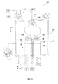
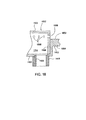
図1は、内部に放射状の冷却流路を有する基板ペデスタルアセンブリ116の一実施形態を有する例示的なエッチリアクタ100の概略図である。この本発明に示されるエッチリアクタ100の特定の実施形態は、説明のためのものであり、本発明の範囲を制限するためのものではない。
FIG. 1 is a schematic diagram of an
主に、エッチリアクタ100は、プロセスチャンバ110、ガスパネル138、コントローラ140を含む。このプロセスチャンバ110は、処理空間を包囲する導電性の本体(ウォール)130及び天井120を含む。ガスパネル138からのプロセスガスは、1つ以上のノズルからなるシャワーヘッドを介してチャンバ110のプロセス空間内に供給される。
The
コントローラ140は、中央処理ユニット(CPU)144、メモリー142、サポート回路146を含む。コントローラ140は、集積回路工場のデータベースと選択的にデータの交換を行うとともに、エッチリアクタ100の各部品とチャンバ110内に実行されるプロセスに結合され、それらを制御する。
The
図示された実施形態において、天井120は実質的に平らな誘電材料である。プロセスチャンバ110の他の実施形態として、他のタイプの天井、例えば、ドーム形状の天井であってもよい。天井120の上には、1つ以上の誘電コイル要素(2つの同軸コイル要素エレメントが説明のため図示されているが)を含むアンテナ112が設けられている。このアンテナ112は、無線周波(RF)プラズマ電力ソース118に第1の整合回路170を介して接続される。
In the illustrated embodiment, the
一実施形態において、基板ペデスタルアセンブリ116は、マウントアセンブリ162、ベースアセンブリ114、及び静電チャック188を含む。マウントアセンブリ162はベースアセンブリ114をプロセスチャンバ110に結合する。
In one embodiment, the
静電チャック188は、主に、セラミック及び同様の誘電材料から形成されており、電源128を用いて制御される少なくとも1つのクランピング電極186を含む。更なる実施形態において、この静電チャック188は、第2の整合回路124を介して基板バイアスの電源122に接続される、少なくとも1つのRF電極(図示せず)を含むかもしれない。静電チャック188は、選択的に1つ以上の基板ヒーターを含みうる。一実施形態において、同軸のヒータ184A、184Bにより示されるような、2つの同軸の、独立に制御可能な抵抗性ヒータが、基板150の端から中央までの温度プロファイルを制御するのに用いられる。
The
静電チャック188は、更に、このチャックの基板支持表面に形成され、熱伝導(若しくは、バックサイド)ガスのソース148に流通可能に接続される溝などの複数のガスの通路(図示せず)を含む。動作状態において、バックサイドガス(例えば、ヘリウム(He))が静電チャック188と基板150との間の熱の伝導を向上させるために、制御された圧力により、ガスの流路に供給される。従来どおり、少なくとも静電チャックの基板支持表面には、基板の処理の間に用いられる化学物質及び温度に対し耐久性のあるコーテイングが施されている。
The
ベースアセンブリ114は、主にアルミニウム若しくは他の金属材料から形成される。ベースアセンブリ114は、加熱若しくは冷却の液体のソース112に結合された1つ以上の冷却通路を含む。フレオン、ヘリウム、若しくは、窒素などの少なくとも1つのガス、あるいは、水若しくは油などの液体であるかもしれない熱伝導液体は、ベースアセンブリ114の温度を制御するために通路を介してソース182により供給され、これにより、ベースアセンブリ114を加熱若しくは冷却し、これにより、処理の間にベースアセンブリ114上に置かれた基板150の温度を部分的に制御する。
ペデスタルアセンブリ116及び基板150の温度は、複数のセンサ(図1に図示せず)を用いて監視される。ペデスタルアセンブリ116によるセンサの設置については、更に、以下に説明される。光ファイバーによる温度センサがペデスタルアセンブリ116の温度プロファイルを示す測定値を提供するためにコントローラ142に接続される。
The temperature of the
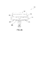
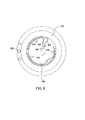
図2A−Bは、基板ペデスタルアセンブリ116に対する均一な温度制御を提供するために構成された冷却流路200を図示する、基板ペデスタルアセンブリ116の一実施形態の概略断面図及び上面図である。基板ペデスタルアセンブリ116は、ベースアセンブリ114上に置かれた静電チャック188を含む。流路200はベースアセンブリ114を介して形成された1つ以上の通路により形成されるかもしれない。流路200はベースアセンブリ114の中に、主に放射状に設けられるかもしれない。図2Aに示された流路200は、ソース182からもたらされる熱伝導流体が放射状に外側に流れるように中央の入口を有しているが、この流れの方向は反対であってもよい。
2A-B are schematic cross-sectional and top views of one embodiment of a
一実施形態において、流路200は第1の放射状通路202及び第2の放射状通路204を含む。この第1及び第2の放射状通路202、204は、実質的に反対の方向に熱伝導流体の流れの方向を方向づけるよう構成される。ベースアセンブリ114は、主に第1及び第2の放射状通路202、204が、半導体基板装置の端のところで良好な温度制御をもたらすように、チャック188及び基板150の外側の直径を超えて放射状に延伸するように、静電チャック188の直径より大きい直径を有する。
In one embodiment, the
図2A−Bに示された実施形態において、第1の放射状通路202は、静電チャック188に接触するベースアセンブリ114の表面の近傍にあるが、第2の放射状通路204は第1の放射状通路202の下に設けられている。一実施形態において、流路200はキノコ状の形状、例えば、実質的にトーラスの形状を有する。流路202のドーナツ形状は、複数の個別の放射状通路、若しくは、単一の通路を含むかもしれない。
In the embodiment shown in FIGS. 2A-B, the first
ドーナツ形状により、従来のベースに用いられてきた流路の長さは大幅に削減しうる。例えば、300ミリの基板を処理するに適した、比較的大きめの大きさのベースにおいて、本発明の一実施形態の流路の構成により、従来の基板支持体のベースにおいて必要とした、およそ72インチから、約6インチに流路の長さが削減されうる。この長さにおける削減により、冷却通路の入口及び出口の温度勾配を削減でき、これにより、基板サポートペデスタル内の温度の勾配を削減することができる。一実施形態において、冷却通路の入口及び出口の間の温度差は、従来の基板支持体において約7℃から約17℃であったのに対し、約0.1から約1.0となる。この流体の入口温度の幅は(−)30から約(+)85℃の間などの、(−)100℃から約(+)200℃の間でありうる。また、この放射流路の構成により、流れに対する抵抗は大きく減少し得、これにより選択された動作圧力において、流動性が向上し、より高い熱伝導率がもたらされる。 Due to the donut shape, the length of the channels used in conventional bases can be significantly reduced. For example, in a relatively large base suitable for processing a 300 mm substrate, the flow path configuration of one embodiment of the present invention provides approximately 72 as required in a conventional substrate support base. The channel length can be reduced from inches to about 6 inches. This reduction in length can reduce the temperature gradient at the inlet and outlet of the cooling passage, thereby reducing the temperature gradient within the substrate support pedestal. In one embodiment, the temperature difference between the inlet and outlet of the cooling passage is about 0.1 to about 1.0, compared to about 7 ° C. to about 17 ° C. in a conventional substrate support. The fluid inlet temperature range can be between (−) 100 ° C. and about (+) 200 ° C., such as between (−) 30 and about (+) 85 ° C. Also, the configuration of this radiating channel can greatly reduce the resistance to flow, thereby improving fluidity and resulting in higher thermal conductivity at the selected operating pressure.
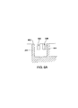
図3は、図1のベースアセンブリ114の断面図である。一実施形態において、ベースアセンブリ114は方向において実質的に放射状である内部冷却流路300を含む。別の実施形態において、流路300は流路200に関連して説明されたと同様に構成されてもよい。
FIG. 3 is a cross-sectional view of the
一実施形態において、ベースアセンブリ114は、トップカバーブレート302、ベースプレート304、チャネル分離プレート306及びボトムカバープレート308を含む。プレート302、304、306、308は主に、例えば、ステンレススチール若しくはアルミニウムなどの金属等良好な熱導伝体から作られる。
In one embodiment, the
トップカバープレート302は、ベースプレート304の上面に形成された凹み部分310に置かれる。凹み部分310の深さは、トップカバープレート302の上表面328がベースプレート304の上部表面312と同一平面となるように選択される。静電チャック188(図3には図示せず)は、トップカバープレート302の上表面328の少なくとも一部において支持される。
The
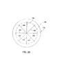
更に、図4に示されるベースプレート114の上面図を参照すると、トップカバープレート302は複数の穴を有する。この穴は、リフトピンのためのもの、及び、静電チャック188にベースセンブリ114を介してヒータ、センサ、ガス、電力などの様々なユーティリィティを供給するためのものである。図4に図示された実施形態において、穴314はリフトピンのために設けられており、穴316はチャックへの電力供給のために設けられており、穴318はヒーターエレメントのために設けられており、穴320は温度センサのために設けられており、穴324、326はトップカバープレート302と静電チャック188との間の熱伝導をもたらすためのものである。同じ参照番号が、同じ役割を果たすための、ベースアセンブリ114の他の部品の穴を識別するために用いられるかもしれない。
Furthermore, referring to the top view of the
ベースプレート304は、複数のマウンテイングホール332が形成される段差330を含む。このマウンテイングホール332は、明確にするためにその1つが図示されているが、一般に段差330において、ボルト円形状に配置される。段差330は、外側に延び出るように、かつ、ベースプレート302の上面312の下方に設けられており、従って、基板150の端を超えて外側に延び出ている。
The
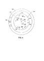
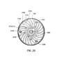
図5は、ベースプレート304の窪んだ表面340を露出させるためにカバープレート302が外された状態の基板ペデスタル114の上面図である。この凹んだ表面340はその中に形成された複数の冷却チャネルを含む。図5に図示された実施形態において、内側の冷却チャネル502及び外側の冷却チャネル504が提供される。ヘリウム、若しくは、他の熱伝導ガス、又は、液体は、それぞれの入口506、508を介して冷却チャネル502、504に供給される。この熱伝導ガスは、チャネル502、504を介して、(図4に図示された)カバープレート302内の複数の穴324、326に分配され、その複数の穴を介して、熱伝導ガスが静電チャック188とベースアセンブリ114との間に分配される。チャネル502、504内の液体の温度は、中央から端までの基板の温度を制御するために、独立に温度制御されるかもしれない。
FIG. 5 is a top view of the
図3に戻ると、ベースプレート304は、ベースプレート304の底336に形成されたキャビテイ334を含む。ボトムカバープレート308は、チャネル分離プレート306をキャビテイ334内に封止するために、ベースプレート304の底336に封止結合される。一実施形態において、ボトムカバープレート308は、ベースプレート304のボトム336に形成された段差338に置かれ、連続溶接、若しくは、他の適宜な技術によりベースプレート304に封着される。
Returning to FIG. 3, the
チャネル分離プレート306は、キャビテイ334を2つの円盤状プレナム342、344に分離する。プレナム304、334は、垂直に重ねられ、キャビテイ344の外側の側壁346とチャネル分離プレート306の外側の端との間のギャップ346を介して流通可能に結合される。図3に図示された実施形態において、放射状の冷媒の流路は、上側のプレナム342からギャップ348を介して下側のプレナム344へと形成される。また、その流路を介する流れの方向は反対向きにもされうる。
A
一実施形態において、チャネル分離プレート306は、複数のスペーサ354により、キャビティ334の上側壁面352から少し離れた位置に維持される。スペーサ354はベースプレート304の一部分である。スペーサ354の少なくともいくつかは、上側のプレナム342による流れが放射状に方向づけられるように、放射状の方向性を有する。
In one embodiment, the
図6は上側壁面352から突出するスペーサ354を図示する、ベースプレート304の平面図を図示する。少数のスペーサ354のみが、説明を明解にするために図示されているが、スペーサ354はベースプレート304の中心線の周り360度に分配配置される。スペーサ354の少なくともいくつかは上側壁面352とチャネル分離プレート306との間の空間を橋渡しする。スペーサ354の数、方向、配置、サイズは、上側プレナム340の液体にベースプレート304からの熱伝導が、所望のプロファイルにより、もたらされるよう選択されるかもしれない。図6に示された実施形態において、スペーサ354は延長され、放射状の流れの方向にあった、主軸を有する。また、スペーサ354は、ベースプレート304の中央線からの同じ半径上のところに位置する2つの隣接するスペーサ354の間を通過する流れが、次の外側のスペーサ354に向かって方向付けられるように、断続的に配置され、これにより、流れが外側に、ギャップ348の方向に行くにつれ、いくらかの横方向の動きを引き起こし、冷却液体を混ぜあわすこととなる。
FIG. 6 illustrates a plan view of the
更に、図6に示されるように、様々な穴314、316、318、320、322、324、326が、それを介して延び出る複数のボス602がある。このボス602は、穴とプレナム304との間のバリアをもたらす。このボス602は、ペデスタルアセンブリ116を介して、ユーティリィティ、センサ、ヒータ、液体の配線・配管のために、ベースカバープレート308の外側にあるボス702(図7に図示)と合致する位置にある。ボトムカバープレート308とベースプレート304との間の接合部は、穴に液体が入り込まないように、溶接されるか、若しくは、別な適宜な方法で封止される。
Further, as shown in FIG. 6, there are a plurality of
図6A−Bの詳細な図を更に参照すると、流れ方向付け器604は、ボスの後ろ側の周りでプレナム342を介して流れる熱伝導液体の巻き込みを促進するために、ボス604の各々の下流側に設けられるかもしれない。一実施形態において、流れ方向付け器604は、スペーサ354の方向とほぼ垂直の方向性を有する。流れ方向付け器604は、更に、図6Aに示される矢印によって示されているように、ボス602と流れ方向付け器604との間に向かう流れを逃がし、ボス602と方向付け器604との間に流れが維持されるようにする。選択的に、流れ方向付け器604は、チャネル分離プレート306と、ベースプレート304の上側壁面352との間の空間を全て遮るものではなく、これによりボス602と方向付け器604との間の液体の一部分が方向づけ機604を通過して逃れるようなダムのような役割を果たす。液体の巻き込みがボス604からの良好な熱伝導を促進し、穴のボイドによる低い熱伝導率を補償する。
With further reference to the detailed views of FIGS. 6A-B, a
図8はチャネル分離プレート306の一実施形態の上面図である。チャネル分離プレート306は、ベースプレート304のボス602が延伸するところの複数の穴802を含む。また、このチャネル分離プレート306は、1つ以上の入口穴804を含み、更に詳細に説明されるように、これによりキャビテイ334への冷却媒体の流入が可能となる。
FIG. 8 is a top view of one embodiment of the
図9−10はチャネル分離プレート306の底面図及び底面の斜視図である。チャネル分離プレート306は入口穴304への熱伝導液体を提供するための横方向へのフィード908を含む。この横方向のフィード908は、ペデスタルアセンブリ116の熱伝導液体の入口をペデスタルの中央からずらし、これにより、電気的配線、リフトピン、ガスチャネルなどの目的のために有効に活用できるスペースができる。図9に図示された実施形態において、横方向のフィード908はチャネル分離プレート306の底から突出するウォール916により区画される。このウォール916は、通常、中空であり、犬用の骨の形状であり、横方向のフィード908の一方の端部のところで外側プレナム910を囲み、横方向フィード908の他方の端のところで内側プレナム912を囲み、このプレナム910、912を流体流通可能に結合するチャネル部分を有する。外側のプレナム910は、概ね、チャネル分離プレート306の中央から外側に位置している。外側プレナム910は(図3及び12に図示されるように)ボトムカバープレート308に形成された液体入口穴309と位置合わせされる。内側のプレナム912は、概ね、チャネル分離プレート306の中央部のところに位置する。内側のプレナム912を取り囲むウォール916の一部分は、入口穴804を取り囲むのに十分幅広く、横方向のフィード908からの液体は、チャネル分離プレート306内の穴804を介して、チャネル分離プレート306の上側に区画された中央分配プレナムの方向へと方向づけられる。
9-10 are a bottom view and a bottom perspective view of the
図11は中央の分配プレナム1102の一実施形態を図示する、ベースアセンブリ114の拡大された断面図である。中央の分配プレナム1102は、底は、チャネル分離プレート306により、上側は、ベースプレート304により囲まれている。ウォール1106は、ベースプレート304から下方向に延び、中央の分配プレナム1102の外側の境界を提供する。ウォール1106は、穴804がプレナム902と1102との間に液体の通路を提供することができるように、ホール804の外側に位置する。このウォール1106は、矢印1104により示されるように、中央の分配プレナムから、上側のプレナム342へ、放射状に液体を逃すよう構成される。
FIG. 11 is an enlarged cross-sectional view of the
一実施形態において、ウォール1106はホール若しくはスロットなどの1つ以上の通路を含み、この通路を介して液体は中央の分配プレナム1102から上側のプレナム342へ流れることができる。一実施形態において、通路1110はスルーホールである。図11に図示された実施形態において、ウォール1106は、おおよそ円筒形の形状であり、その先端部に形成された通路1110を有する。この通路1110はウォール1106に沿って等間隔に設けられる。選択的に、1つ以上の通路1110が全ての放射状の方向に均等に方向づけられることが可能なように連続的なダムとして構成されるかもしれない。また選択的に、通路1110の数及び間隔は、もし必要ならば、上側プレナム342の他の領域より、上側のプレナム342の一領域に、より流れるよう方向づけられるように選択されるかもしれない。
In one embodiment, the
また、図11に示されるように、ベースプレート306はプレナム912、1102内の液体から中央の通路1112を分離するセンターボス1108を含む。この中央の通路1112は、トップカバープレート302を介して形成される穴316及びボトムカバープレート308を介して形成される穴1118と位置合わせされる。通路1112、穴316、及び、穴1118により、ペデスタルアセンブリ116を介して、静電チャック118への電気配線等が可能となる。ボトムカバープレート308とボス1108との間の結合部分は、通路への液体の流れを防ぐために、溶接、又は、他の適宜な方法により封止されるかもしれない。図11のボス1114に示されるように、ボトムカバープレート308のボス702の1つは、電気配線等のための導管を結合を可能ならしめるために、その中に形成されたポート1116を有する。他のボス702も同様に構成される。
Also, as shown in FIG. 11, the
ペデスタルアセンブリ116を介しての流路の液体の出口が、図12の部分断面図に示されている。液体出口のための穴1202は、下側のプレナム344からの排出のために、ボトムカバープレート308に形成される。一般に、出口のための穴1202は入口のための穴398の近くに位置する。図12中の入口ボス1204及び出口ボス1206に示されるように、ボトムカバープレート308上に形成されたボス702の2つは、ホール398、1202を介して流路300への液体流通をもたらすために用いられる。一実施形態においてボス1204は、熱伝導液体ソース182に接続されるとともに、一方でボス1206は廃液管に結合されるか、液体ソース182に戻され再利用される。流路300を介して提供される冷却液体の熱伝導媒体の圧力、流量、温度、濃度、成分は、ペデスタルアセンブリ116による熱伝導プロファイルの制御を向上せしめる。更に、流路300内の液体の濃度、圧力、流量は、基板150の処理の間、インシュチュ(in-situ)により、その場で制御されうるので、基板150の温度制御は、更に処理能力を高めるために処理中に変化させてもよい。
The fluid outlet of the flow path through the
動作中において、基板150はペデスタルアセンブリ116の上に置かれる。基板を固定するために静電チャック188に電力が供給される。電力は静電チャック188内のヒーターに供給され、基板150の横方向の温度の制御が可能となる。液体、及び/又は、フレオンなどのガスであるかもしれない冷却液体は、ベースアセンブリ114内に区画された放射状の冷却通路を介して供給され、基板の正確な温度制御が可能となる。
In operation, the
一実施形態において、冷却媒体は中央の分配プレナム1102に供給され、それから冷却媒体は1つ以上の通路1110を介して円盤形状の上側のプレナム342に分配される。流れ方向付け器604は、プレナム342内に延伸する様々なボス604の周りを巡って上側プレナム342内を流れる熱伝導液体の巻き込みを促進するのに用いられる。そして、冷却媒体は、ギャップ348を介して、上側342から下側の円盤形状のプレナム344へと流れ、それから冷却媒体は最終的に取り除かれる。流れの方向を交差させると共に、冷却媒体の流路が放射状に構成されることにより、冷却媒体の通路の長さを削減し、圧力の低下を削減し、ペデスタルアセンブリ116に対する冷却の均一性を高めることに効果的に寄与し、これによりリアクタ100内のより改善されたプロセス制御が可能となる。
In one embodiment, the cooling medium is supplied to the
例えば、以上に述べられた基板温度制御は、ガスパネル138から供給されるガスからリアクタ100内においてプラズマが形成されるようなエッチングのプロセスに用いられるかもしれない。また、真空チャンバ内で実行される上述したような、及び/又は、正確な温度制御が必要とされる他の基板製造プロセスにおいても、本明細書に記述される温度制御方法及び装置の利用により効果が得られるかもしれない。
For example, the substrate temperature control described above may be used in an etching process in which plasma is formed in the
図13はベースアセンブリ1300の他の実施形態の展開された斜視図であり、このベースアセンブリを介して、熱伝導液体が上側の円盤状のプレナムから、下側の円盤状プレナムへ流れ、そこから最終的には液体が取り除かれる。このベースアセンブリ1300はベースプレート1302、チャネル分離プレート1304、及び、ボトムカバープレート1306を含む。ベースプレート1302及びボトムカバープレート1306はその間でチャネル分離プレート1304を保持して、共に密着して結合され、チャネル分離プレートとベースプレートとの間に流れ込む冷却液体が外側へ、チャネル分離プレート1304の外側直径1314を超えてチャネル分離プレート1304とボトムカバープレート1306との間に区画されたボトムプレナムに流れ込むようにする。ベースプート1302、チャネル分離プレート1304、及びボトムカバープレート1306はすべてベースプレート1302の上部1316に結合される静電チャック188(図1に示す)への電力他のユーティリティーへの接続のための導管を提供する中央の開口1308を含む。
FIG. 13 is an exploded perspective view of another embodiment of a
また、ベースプレート1302及びボトムカバープレート1306は、複数のリフトピンのためのホール1310を含む。チャネル分離プレート1304はチャネル分離プレート1304がリフトピンの動作に邪魔しないように、リフトピンのホール1310と位置合わせされた位置に、外側直径1314に形成された複数の切り込み1312を含む。
In addition, the
更に、ベースプレート1302の上面1316は内側のチャネル1318と外側の冷却チャネル1320を含む。内側のチャネル1318はベースプレートを介して形成された入口1322を介して液体が流される。外側のチャネル1320はベースプレート1302を介して形成された入口1324を介して液体が流される。冷却液体フィード1328、1330はボトムカバープレート1306内に設けられ、入口1320、1322に位置合わせされ、ヘリウム、窒素などの液体がベースアセンブリを介して冷却チャネル1312、1322へ回り込むようにし、アセンブリ1300と静電チャック118との間の熱伝導を高める。開口1326はチャネル分離プレート1304に設けられ、冷却媒体供給路1328、1330を入口1322、1324に結合せしめる。
Further, the
また、通路1332はベースプレート1302、チャネル分離プレート1304、及びボトムカバープレート1306を介して設けられ、熱伝達を可能とする。更に、このボトムカバープレート1306は、一対の開口1334、1336を含み、以下に詳述するように、ベースアセンブリ1300への、又は、それからの冷却液体の流れを可能ならしめる。
The
図14−16はチャネル分離プレート1304の底面図、上面図、側面図である。チャネル分離プレート1304は底面1402及び上面1602を含む。第1のボス1404は底面1402から延び出て、チャネル分離プレート1304の上面1602にへこみが形成される。第1のボス1404に形成された凹みはチャネル分離プレート1304の上面1602から延び出る入口マニフォルドケージ1502の一部分を受容する。第2のボス1406はチャネル分離プレート1304の底面1402からの第1のボス1404から延び出る。第2のボス1406はチャネル分離プレート1304を介して形成された通路1408を含む。通路1408により、液体がベースアセンブリ1300に流れ込むことができ、入口マニフォルドケージ1502を介して、チャネル分離プレート1304とベースプレート1302との間に区画された上側のプレナムに流れ込むことができる。
14-16 are a bottom view, a top view, and a side view of the
入口マニフォルドケージ1502は側面1504及び上面1506を含む。複数の窓1508が入口マニフォルドケージ1502の側面1504に形成され、通路1408を介してベースアセンブリ1300に流れ込む液体の流れがチャネル分離プレート1304とベースプレート1302との間に区画された上側プレナムに流れることを容易にする。窓1508は液体がそこを流れることを可能にするために適宜な穴、スロット又は他の形状であってもよい。
入口マニフォルドケージ1502は中央の開口1308を取り囲むリング1604を含む。突出部分1606がリング1604の外側の直径上に形成され、第2のボス1406を介して形成される通路1408と位置合わせされ、第2のボス1406により方向づけられた液体が入口マニフォルドケージ1502に区画された空間に入るようにする。
The
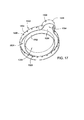
図17は入口マニフォルドケージ1502の一実施態様の側面斜視図である。入口マニフォルドケージ1502は側面1504により取り囲まれる円環状の内部ウォール1702を含む。入口マニフォルドケージ1504の内部ウォール1702、側面1504、上面1506は、マニフォルドケージ1502内に、液体通路1704を形成する。
FIG. 17 is a side perspective view of one embodiment of the
図18はチャネル分離プレート1304と入口マニフォルドケージ1502の部分側面断面図である。図18の実施態様と対応に示されるように、入口マニフォルドケージ1502は第1のボス1404内に形成された窪み内に部分的に係合する。窓1508は上面1506の近傍にある、入口マニフォルドケージ1502の側面1504に沿って配置されており、窓1508はチャネル分離プレート1304の上面1602に液体を供給するよう位置する。このようにして、ボス1406により形成される通路1408から液体通路1704に入り込む液体は、側面1504から放射状に外側の方向に上側プレナムに容易に流れ込むことができる。
FIG. 18 is a partial side cross-sectional view of the
図19−21はボトムカバープレート1306の一実施態様の底面、側面、上面図である。ボトムカバープレート1306の底面1902は、ボトムカバープレート1306の熱質量を低減するために、その中に形成された複数のキャビテイ1904を含み、これにより、アセンブリ1300はより、急速に加熱され、及び、冷却される。更に、ボトムカバープレート1306は、ベースアセンブリ1300に入ったり、又は、そこから出たりする冷却液体の回り込みを容易にするため形成される2つの穴1906、1908を含む。この穴1906はチャネル分離プレート1304から延び出るボス1406を受容するに十分な大きさのものである。穴1908は、ボトムカバープレート1306とチャネル分離プレート1304との間に形成される下側のプレナムへの流れ込みを容易にする。穴1908は底面1902上のカウンターの穴2158を含み、係合部品との位置合わせを容易にするかもしれない。
FIGS. 19-21 are bottom, side and top views of one embodiment of the
ボトムカバープレート1306の上面2002は第1のボス2004と第2のボス2006を含む。第1のボス2004は中央の開口1308を取り囲む。第2のボス2006は温度の検知に用いられるために形成された通路1332を有する。また、ボトムカバープレート1306は、ボトムカバープレート1306の温度を検知するのに使われる温度プローブを収容するための第2の穴1910を含むかもしれない。
An
図22はベースアセンブリ1300の部分側断面を含む斜視図である。図22に図示された実施態様において、ベースプレート1302はベースプレート1302の底の面から延び出るリップ2250を含む。リップ2250は内側の壁2254を含み、その壁はチャネル分離プレート1304及びボトムカバープレート1306が収容されるポケット2256を形成する。ボトムカバープレート1306のリップ2250は、例えば、連続的な溶接、若しくは、他の適宜な技術によって、ベースプレート1302に封止され、アセンブリ1300内での上側及び下側のプレナムを介して流れる液体を維持する。ポケット2256はチャネル分離プレート1304が設けられた底2258を有する。また、この底2258は、その中に形成された複数のチャネル2208を分離する複数のフィン2206を含む。このフィン2206及びチャネル2208については、図23−26を参照して以下により詳細に説明される。チャネル2208はチャネル分離プレート1304とベースプレート1302の底面2258との間に区画された下側プレナム2220の多くの部分を多くを区画する。液体は、入口マニフォルドケージ1502内に形成された窓1508を介して上側プレナム2220に流れ込む。液体は入口マニフォルドケージ1502から、上側プレナム2220のチャネル2208を介して、端部1314を周り、チャネル分離プレート1304の端部1314とベースプレート1302の内側ウォール2254との間に区画された溝2114へと流れる。液体は溝2114からボトムプレナム2222へ流れ、ボトムカバープレート1308を介して形成された穴1908に流れ出る。このように、ベースアセンブリ1300のプレナム2220、2222を介した流れのパターンは実質的に図2A−2Bを参照して説明されたベースアセンブリ114と類似のものである。
FIG. 22 is a perspective view including a partial side cross section of the
ボトムカバープレート1306は内側ウォール2254内に形成された1対の段差2252、2262、及び、底面2258から延び出て、中央の開口1308を取り囲むボス2260の上に位置する。この段差2252、2262はチャネル分離プレート1304及びボトムカバープレート1306を所定間隔、離して維持し、これにより下側プレナム2222を介して液体が流れるための十分な空間をもたらす。
The
図23−26はベースアセンブリ1300のベースプレート1302の選択的な底面の図である。図23−26の実施態様に共通なものは、チャネル2208の実質的に放射状の方向性と、プレナム2220、2222を介する流れの反対の放射状の方向性である。
23-26 is an optional bottom view of
複数のパッド2210がベースプレート1302の底面の表面から延び出る。一実施態様において、7つのパットがフィン2206の上に延び出るように示されている。パッド2210は、ベースプレート1302とチャネル分離プレート1304との間に間隙を残して設けられ、これにより、チャネル分離プレート1304とフィン2206との間に小さいギャップが形成されるので、ベースプレート1302とチャネル分離プレート1304との間の直接的な熱伝導が最小限となる。
A plurality of
図23に示された実施形態において、チャネル2208は、ベースプレート1302の底面で外側に放射状に延びる長さに亘り、実施的に均一の幅の、及び/又は、断面領域を有する。この実質的に均一なチャネルの幅を可能とするために、フィン2206は外に向かって広がっており、フィンがベースプレート1302の外側の端に近づくほど次第に幅広くなる。チャネル2208は線形であったり、曲がっていたり、放射状に曲がっていたり、若しくは、他の方向性を有してもよい。図23に示された実施態様において、チャネル2208は曲がっており、チャネル2208を介して流れる液体は、上側のプレナム2220内でのより長い残存時間を有し、これにより熱伝導効率を増加せしめる。
In the embodiment shown in FIG. 23, the
図24に示された実施態様において、チャネル2208はメインチャネル2402及びそこから分岐する複数のサブチャネル2404を含む。図24に示された実施態様において、少なくとも2つのサブチャネルが示されている。しかしながら、メインチャネル2402は、3つ以上のサブチャネル2404を有し得、サブチャネルそれ自体が2つ若しくはそれ以上の第2のチャネル(図示せず)に分岐するかもしれない。サブチャネルはチャネル間フィン2406に分離される。
In the embodiment shown in FIG. 24,
図25に示された実施態様において、複数のチャネル2502が複数のフィン2504に分離されて示されている。チャネル2502は、チャネル2502が放射状に外側に向かうにつれ、均一の断面領域、及び/又は、幅を有するかもしれない。選択的に、このチャネル2502の断面領域、及び/又は、幅は、チャネル2502がベースプレート1302の外側の直径に近づくにつれ、広がるかもしれない。図25に示された実施態様において、チャネル2502を分離するフィン2504は、実質的にブーメランの形であり、各フィンの端と反対にフィン2504の中央部分ではより厚くなっている。このブーメラン型により、より深く曲がったチャネル2502が可能となり、これにより実質的に上側プレナム2220内に液体の残存時間を増加せしめることができる。
In the embodiment shown in FIG. 25, a plurality of
図26に示された実施態様において、複数のチャネル2602が複数のフィン2604により分離されて示されている。各フィン2604は、フィン2604が放射状に外側に向かうにつれ、その断面領域、及び/又は、幅において均一である。従って、チャネル2602はそれらがベースプレート1302の端に向かうにつれ、広がる。フィン2604は放射方向において線形に延びるかもしれない、又は、それらは曲げられ、上側プレナム2220を形成するチャネル2602内での冷却液体の残存時間を増加せしめるかもしれない。
In the embodiment shown in FIG. 26, a plurality of
このように、放射状の冷却流路を含むペデスタルアセンブリがもたらされる。ペデスタルアセンブリを介する放射状の冷却流路は、改善された温度制御をもたらし、これにより、基板の温度プロファイルの制御が可能となる。 In this way, a pedestal assembly is provided that includes radial cooling channels. The radial cooling flow path through the pedestal assembly provides improved temperature control, which allows control of the temperature profile of the substrate.
本発明の実施態様に沿って説明されてきたが、本発明の他の更なる実施態様は本発明の基本範囲を逸脱することなく創作されることができ、その範囲は以下の特許請求の範囲に基づいて定められる。 While described in connection with embodiments of the invention, other and further embodiments of the invention may be made without departing from the basic scope of the invention, which is encompassed by the following claims It is determined based on.
Claims (15)
真空処理チャンバ内で基板ペデスタルアセンブリ上に基板を載置し、
前記基板ペデスタルアセンブリ内の放射状の流路を介して熱伝導液体を流すことにより前記基板ペデスタルアセンブリの温度を制御し、前記放射状の流路は内側に放射状になっている部分、及び、外側に放射状になっている部分を含み、
前記温度制御された基板ペデスタルアセンブリ上で前記基板をプラズマ処理することを含む方法。 A method for controlling the temperature of a substrate during processing, comprising:
Placing the substrate on the substrate pedestal assembly in a vacuum processing chamber;
The temperature of the substrate pedestal assembly is controlled by flowing a heat transfer liquid through a radial flow path in the substrate pedestal assembly, and the radial flow path is radially inward and radially outward. Including the part which becomes
Plasma treating the substrate on the temperature controlled substrate pedestal assembly.
前記基板ペデスタルアセンブリの中央に設けられたプレナムに前記熱伝導液体を流し、
前記プレナムから実質的に円盤形状のプレナムに、外方向に放射状に前記熱伝導液体を流すことを含む請求項1記載の方法。 To control
Flowing the thermally conductive liquid through a plenum provided in the center of the substrate pedestal assembly;
The method of claim 1 including flowing the thermally conductive liquid radially outwardly from the plenum to a substantially disc-shaped plenum.
前記第1のプレナムの放射状に外側に区画された環状のギャップを介して第2の実質的円盤形状のプレナムに前記熱伝導液体を流すことを含む請求項5記載の方法。 Flowing
6. The method of claim 5, comprising flowing the heat transfer liquid through a second substantially disk-shaped plenum through an annular gap radially outwardly defined in the first plenum.
上面に前記静電チャックが固着されたベースアセンブリであり、前記ベースアセンブリの内側に形成された冷却流路を有するベースアセンブリとを含み、
前記冷却流路は外側に放射状に流れを向けるよう構成されているペデスタルアセンブリ。 An electrostatic chuck;
A base assembly having the electrostatic chuck secured to an upper surface, and a base assembly having a cooling channel formed inside the base assembly;
A pedestal assembly, wherein the cooling channel is configured to direct a flow radially outward.
固着された前記静電チャックを有するベースプレートと、
前記ベースプレートの底に密着して結合されたボトムカバープレートとを含み、
前記冷却流路は、その間に形成にされ、少なくとも1つ円盤形状のプレナムを含む請求項7記載のペデスタルアセンブリ。 The base assembly is
A base plate having the electrostatic chuck secured thereto;
A bottom cover plate that is in close contact with the bottom of the base plate, and
The pedestal assembly of claim 7, wherein the cooling channel is formed therebetween and includes at least one disk-shaped plenum.
固着された前記静電チャックを有するベースプレートと、
前記ベースプレートの底に密着して結合されるボトムカバープレートと、
前記ベースプレートと前記カバープレートの間に設けられたチャネル分離プレートを有し、
前記冷却流路は、前記チャネル分離プレートと前記ベースプレートとの間の少なくとも一部分に形成され、前記チャネル分離プレートと前記ボトムカバープレートとの間の少なくとも一部分に形成されている請求項7記載のペデスタルアセンブリ。 The base assembly is
A base plate having the electrostatic chuck secured thereto;
A bottom cover plate closely attached to the bottom of the base plate;
A channel separation plate provided between the base plate and the cover plate;
The pedestal assembly according to claim 7, wherein the cooling flow path is formed in at least a portion between the channel separation plate and the base plate, and is formed in at least a portion between the channel separation plate and the bottom cover plate. .
前記流路へと延び、実質的に放射方向を有する複数フィンを含み、前記フィンのうちの少なくとも1つは、線形の方向性を有するか、若しくは、曲がっている請求項9記載のペデスタルアセンブリ。 The base plate is
The pedestal assembly of claim 9, comprising a plurality of fins extending into the flow path and having a substantially radial direction, wherein at least one of the fins has a linear orientation or is bent.
その上部表面に固着された前記静電チャックを有するベースアセンブリと、
前記ベースアセンブリに形成された実質的にドーナツ形状の流路であり、前記ベースアッセンブリの底の表面に形成された入口及び出口を有する実質的にドーナツ形状の流路とを含むペデスタルアセンブリ。 An electrostatic chuck;
A base assembly having said electrostatic chuck secured to its upper surface;
A pedestal assembly comprising a substantially donut-shaped channel formed in the base assembly and a substantially donut-shaped channel having an inlet and an outlet formed in a bottom surface of the base assembly.
固着された前記静電チャックを有するベースプレートと、
複数のパッドにより前記にベースに対して離れた間隔に設けられたチャネル分離プレートであり、前記実質的ドーナツ形状の流路は前記チャネル分離プレートの外側の端を超えて延びいるチャネル分離プレートと、
前記チャネル分離プレートに対して離れた間隔を有する前記ベースプレートの底に密着して結合されたボトムカバープレートとを含む請求項12記載のペデスタルアセンブリ。 The base assembly is
A base plate having the electrostatic chuck secured thereto;
A channel separation plate spaced apart from the base by a plurality of pads, wherein the substantially donut-shaped flow path extends beyond an outer end of the channel separation plate;
The pedestal assembly of claim 12, comprising a bottom cover plate that is intimately coupled to a bottom of the base plate that is spaced apart from the channel separation plate.
前記ボトムカバープレートと前記チャネル分離プレートとの間に形成される空間に通じる第1の穴と、
前記ベースプレートと前記チャネル分離プレートとの間に形成される空間に液体流動可能に結合された第1の穴とを含む請求項13記載のペデスタルアセンブリ。 The bottom cover plate is
A first hole that leads to a space formed between the bottom cover plate and the channel separation plate;
The pedestal assembly of claim 13, comprising a first hole coupled in a liquid flowable manner to a space formed between the base plate and the channel separation plate.
Applications Claiming Priority (2)
| Application Number | Priority Date | Filing Date | Title |
|---|---|---|---|
| US1600007P | 2007-12-21 | 2007-12-21 | |
| PCT/US2008/087533 WO2009086013A2 (en) | 2007-12-21 | 2008-12-18 | Method and apparatus for controlling temperature of a substrate |
Publications (2)
| Publication Number | Publication Date |
|---|---|
| JP2011508436A true JP2011508436A (en) | 2011-03-10 |
| JP2011508436A5 JP2011508436A5 (en) | 2014-02-20 |
Family
ID=40787366
Family Applications (1)
| Application Number | Title | Priority Date | Filing Date |
|---|---|---|---|
| JP2010539830A Pending JP2011508436A (en) | 2007-12-21 | 2008-12-18 | Method and apparatus for controlling the temperature of a substrate |
Country Status (6)
| Country | Link |
|---|---|
| US (1) | US20090159566A1 (en) |
| JP (1) | JP2011508436A (en) |
| KR (1) | KR20100103627A (en) |
| CN (1) | CN101903996B (en) |
| TW (1) | TW200937563A (en) |
| WO (1) | WO2009086013A2 (en) |
Cited By (85)
| Publication number | Priority date | Publication date | Assignee | Title |
|---|---|---|---|---|
| KR20150038154A (en) * | 2012-07-18 | 2015-04-08 | 어플라이드 머티어리얼스, 인코포레이티드 | Pedestal with multi-zone temperature control and multiple purge capabilities |
| KR101545119B1 (en) * | 2014-08-14 | 2015-08-18 | (주)얼라이드 테크 파인더즈 | Plasma device |
| JP2017506825A (en) * | 2014-02-12 | 2017-03-09 | アクセリス テクノロジーズ, インコーポレイテッド | Constant mass flow multilayer coolant path electrostatic chuck |
| US9947549B1 (en) | 2016-10-10 | 2018-04-17 | Applied Materials, Inc. | Cobalt-containing material removal |
| US9966240B2 (en) | 2014-10-14 | 2018-05-08 | Applied Materials, Inc. | Systems and methods for internal surface conditioning assessment in plasma processing equipment |
| US9978564B2 (en) | 2012-09-21 | 2018-05-22 | Applied Materials, Inc. | Chemical control features in wafer process equipment |
| US10026621B2 (en) | 2016-11-14 | 2018-07-17 | Applied Materials, Inc. | SiN spacer profile patterning |
| US10032606B2 (en) | 2012-08-02 | 2018-07-24 | Applied Materials, Inc. | Semiconductor processing with DC assisted RF power for improved control |
| US10043674B1 (en) | 2017-08-04 | 2018-08-07 | Applied Materials, Inc. | Germanium etching systems and methods |
| US10043684B1 (en) | 2017-02-06 | 2018-08-07 | Applied Materials, Inc. | Self-limiting atomic thermal etching systems and methods |
| US10049891B1 (en) | 2017-05-31 | 2018-08-14 | Applied Materials, Inc. | Selective in situ cobalt residue removal |
| US10062585B2 (en) | 2016-10-04 | 2018-08-28 | Applied Materials, Inc. | Oxygen compatible plasma source |
| US10062575B2 (en) | 2016-09-09 | 2018-08-28 | Applied Materials, Inc. | Poly directional etch by oxidation |
| US10128086B1 (en) | 2017-10-24 | 2018-11-13 | Applied Materials, Inc. | Silicon pretreatment for nitride removal |
| US10147620B2 (en) | 2015-08-06 | 2018-12-04 | Applied Materials, Inc. | Bolted wafer chuck thermal management systems and methods for wafer processing systems |
| US10163696B2 (en) | 2016-11-11 | 2018-12-25 | Applied Materials, Inc. | Selective cobalt removal for bottom up gapfill |
| US10170336B1 (en) | 2017-08-04 | 2019-01-01 | Applied Materials, Inc. | Methods for anisotropic control of selective silicon removal |
| US10186428B2 (en) | 2016-11-11 | 2019-01-22 | Applied Materials, Inc. | Removal methods for high aspect ratio structures |
| US10224180B2 (en) | 2016-10-04 | 2019-03-05 | Applied Materials, Inc. | Chamber with flow-through source |
| US10224210B2 (en) | 2014-12-09 | 2019-03-05 | Applied Materials, Inc. | Plasma processing system with direct outlet toroidal plasma source |
| US10242908B2 (en) | 2016-11-14 | 2019-03-26 | Applied Materials, Inc. | Airgap formation with damage-free copper |
| US10256112B1 (en) | 2017-12-08 | 2019-04-09 | Applied Materials, Inc. | Selective tungsten removal |
| US10256079B2 (en) | 2013-02-08 | 2019-04-09 | Applied Materials, Inc. | Semiconductor processing systems having multiple plasma configurations |
| US10283321B2 (en) | 2011-01-18 | 2019-05-07 | Applied Materials, Inc. | Semiconductor processing system and methods using capacitively coupled plasma |
| US10283324B1 (en) | 2017-10-24 | 2019-05-07 | Applied Materials, Inc. | Oxygen treatment for nitride etching |
| US10297458B2 (en) | 2017-08-07 | 2019-05-21 | Applied Materials, Inc. | Process window widening using coated parts in plasma etch processes |
| US10319603B2 (en) | 2016-10-07 | 2019-06-11 | Applied Materials, Inc. | Selective SiN lateral recess |
| US10319649B2 (en) | 2017-04-11 | 2019-06-11 | Applied Materials, Inc. | Optical emission spectroscopy (OES) for remote plasma monitoring |
| US10319600B1 (en) | 2018-03-12 | 2019-06-11 | Applied Materials, Inc. | Thermal silicon etch |
| US10319739B2 (en) | 2017-02-08 | 2019-06-11 | Applied Materials, Inc. | Accommodating imperfectly aligned memory holes |
| US10354889B2 (en) | 2017-07-17 | 2019-07-16 | Applied Materials, Inc. | Non-halogen etching of silicon-containing materials |
| US10403507B2 (en) | 2017-02-03 | 2019-09-03 | Applied Materials, Inc. | Shaped etch profile with oxidation |
| US10424485B2 (en) | 2013-03-01 | 2019-09-24 | Applied Materials, Inc. | Enhanced etching processes using remote plasma sources |
| US10424463B2 (en) | 2015-08-07 | 2019-09-24 | Applied Materials, Inc. | Oxide etch selectivity systems and methods |
| US10424487B2 (en) | 2017-10-24 | 2019-09-24 | Applied Materials, Inc. | Atomic layer etching processes |
| US10431429B2 (en) | 2017-02-03 | 2019-10-01 | Applied Materials, Inc. | Systems and methods for radial and azimuthal control of plasma uniformity |
| US10465294B2 (en) | 2014-05-28 | 2019-11-05 | Applied Materials, Inc. | Oxide and metal removal |
| US10468276B2 (en) | 2015-08-06 | 2019-11-05 | Applied Materials, Inc. | Thermal management systems and methods for wafer processing systems |
| US10468267B2 (en) | 2017-05-31 | 2019-11-05 | Applied Materials, Inc. | Water-free etching methods |
| US10468285B2 (en) | 2015-02-03 | 2019-11-05 | Applied Materials, Inc. | High temperature chuck for plasma processing systems |
| JP2019201086A (en) * | 2018-05-15 | 2019-11-21 | 東京エレクトロン株式会社 | Processing device, component, and temperature control method |
| US10490406B2 (en) | 2018-04-10 | 2019-11-26 | Appled Materials, Inc. | Systems and methods for material breakthrough |
| US10497573B2 (en) | 2018-03-13 | 2019-12-03 | Applied Materials, Inc. | Selective atomic layer etching of semiconductor materials |
| US10504700B2 (en) | 2015-08-27 | 2019-12-10 | Applied Materials, Inc. | Plasma etching systems and methods with secondary plasma injection |
| US10504754B2 (en) | 2016-05-19 | 2019-12-10 | Applied Materials, Inc. | Systems and methods for improved semiconductor etching and component protection |
| US10522371B2 (en) | 2016-05-19 | 2019-12-31 | Applied Materials, Inc. | Systems and methods for improved semiconductor etching and component protection |
| US10541184B2 (en) | 2017-07-11 | 2020-01-21 | Applied Materials, Inc. | Optical emission spectroscopic techniques for monitoring etching |
| US10541246B2 (en) | 2017-06-26 | 2020-01-21 | Applied Materials, Inc. | 3D flash memory cells which discourage cross-cell electrical tunneling |
| US10546729B2 (en) | 2016-10-04 | 2020-01-28 | Applied Materials, Inc. | Dual-channel showerhead with improved profile |
| US10566206B2 (en) | 2016-12-27 | 2020-02-18 | Applied Materials, Inc. | Systems and methods for anisotropic material breakthrough |
| US10573496B2 (en) | 2014-12-09 | 2020-02-25 | Applied Materials, Inc. | Direct outlet toroidal plasma source |
| US10573527B2 (en) | 2018-04-06 | 2020-02-25 | Applied Materials, Inc. | Gas-phase selective etching systems and methods |
| US10593523B2 (en) | 2014-10-14 | 2020-03-17 | Applied Materials, Inc. | Systems and methods for internal surface conditioning in plasma processing equipment |
| US10593560B2 (en) | 2018-03-01 | 2020-03-17 | Applied Materials, Inc. | Magnetic induction plasma source for semiconductor processes and equipment |
| US10615047B2 (en) | 2018-02-28 | 2020-04-07 | Applied Materials, Inc. | Systems and methods to form airgaps |
| US10629473B2 (en) | 2016-09-09 | 2020-04-21 | Applied Materials, Inc. | Footing removal for nitride spacer |
| US10672642B2 (en) | 2018-07-24 | 2020-06-02 | Applied Materials, Inc. | Systems and methods for pedestal configuration |
| US10679870B2 (en) | 2018-02-15 | 2020-06-09 | Applied Materials, Inc. | Semiconductor processing chamber multistage mixing apparatus |
| US10699879B2 (en) | 2018-04-17 | 2020-06-30 | Applied Materials, Inc. | Two piece electrode assembly with gap for plasma control |
| US10727080B2 (en) | 2017-07-07 | 2020-07-28 | Applied Materials, Inc. | Tantalum-containing material removal |
| US10755941B2 (en) | 2018-07-06 | 2020-08-25 | Applied Materials, Inc. | Self-limiting selective etching systems and methods |
| US10854426B2 (en) | 2018-01-08 | 2020-12-01 | Applied Materials, Inc. | Metal recess for semiconductor structures |
| US10872778B2 (en) | 2018-07-06 | 2020-12-22 | Applied Materials, Inc. | Systems and methods utilizing solid-phase etchants |
| US10886137B2 (en) | 2018-04-30 | 2021-01-05 | Applied Materials, Inc. | Selective nitride removal |
| US10892198B2 (en) | 2018-09-14 | 2021-01-12 | Applied Materials, Inc. | Systems and methods for improved performance in semiconductor processing |
| US10903054B2 (en) | 2017-12-19 | 2021-01-26 | Applied Materials, Inc. | Multi-zone gas distribution systems and methods |
| US10920319B2 (en) | 2019-01-11 | 2021-02-16 | Applied Materials, Inc. | Ceramic showerheads with conductive electrodes |
| US10920320B2 (en) | 2017-06-16 | 2021-02-16 | Applied Materials, Inc. | Plasma health determination in semiconductor substrate processing reactors |
| US10943834B2 (en) | 2017-03-13 | 2021-03-09 | Applied Materials, Inc. | Replacement contact process |
| US10964512B2 (en) | 2018-02-15 | 2021-03-30 | Applied Materials, Inc. | Semiconductor processing chamber multistage mixing apparatus and methods |
| US11049755B2 (en) | 2018-09-14 | 2021-06-29 | Applied Materials, Inc. | Semiconductor substrate supports with embedded RF shield |
| US11062887B2 (en) | 2018-09-17 | 2021-07-13 | Applied Materials, Inc. | High temperature RF heater pedestals |
| US11121002B2 (en) | 2018-10-24 | 2021-09-14 | Applied Materials, Inc. | Systems and methods for etching metals and metal derivatives |
| US11239061B2 (en) | 2014-11-26 | 2022-02-01 | Applied Materials, Inc. | Methods and systems to enhance process uniformity |
| US11257693B2 (en) | 2015-01-09 | 2022-02-22 | Applied Materials, Inc. | Methods and systems to improve pedestal temperature control |
| US11276559B2 (en) | 2017-05-17 | 2022-03-15 | Applied Materials, Inc. | Semiconductor processing chamber for multiple precursor flow |
| US11276590B2 (en) | 2017-05-17 | 2022-03-15 | Applied Materials, Inc. | Multi-zone semiconductor substrate supports |
| US11328909B2 (en) | 2017-12-22 | 2022-05-10 | Applied Materials, Inc. | Chamber conditioning and removal processes |
| US11417534B2 (en) | 2018-09-21 | 2022-08-16 | Applied Materials, Inc. | Selective material removal |
| US11437242B2 (en) | 2018-11-27 | 2022-09-06 | Applied Materials, Inc. | Selective removal of silicon-containing materials |
| KR20230006314A (en) * | 2021-07-02 | 2023-01-10 | 광운대학교 산학협력단 | Substrate processing apparatus and temperature control method using multi-zone heat transfer structure |
| KR20230006311A (en) * | 2021-07-02 | 2023-01-10 | 광운대학교 산학협력단 | Substrate processing apparatus and temperature control method using heat transfer structure |
| US11594428B2 (en) | 2015-02-03 | 2023-02-28 | Applied Materials, Inc. | Low temperature chuck for plasma processing systems |
| US11682560B2 (en) | 2018-10-11 | 2023-06-20 | Applied Materials, Inc. | Systems and methods for hafnium-containing film removal |
| US11721527B2 (en) | 2019-01-07 | 2023-08-08 | Applied Materials, Inc. | Processing chamber mixing systems |
Families Citing this family (36)
| Publication number | Priority date | Publication date | Assignee | Title |
|---|---|---|---|---|
| US7221553B2 (en) * | 2003-04-22 | 2007-05-22 | Applied Materials, Inc. | Substrate support having heat transfer system |
| US20060105182A1 (en) * | 2004-11-16 | 2006-05-18 | Applied Materials, Inc. | Erosion resistant textured chamber surface |
| WO2011056433A2 (en) * | 2009-11-03 | 2011-05-12 | Applied Materials, Inc. | Temperature control of a substrate during a plasma ion implantation process for patterned disc media applications |
| JP2011184738A (en) * | 2010-03-09 | 2011-09-22 | Fujifilm Corp | Method for producing gas barrier film |
| US8772103B2 (en) * | 2010-10-25 | 2014-07-08 | Texas Instruments Incorporated | Low temperature implant scheme to improve BJT current gain |
| US9719169B2 (en) * | 2010-12-20 | 2017-08-01 | Novellus Systems, Inc. | System and apparatus for flowable deposition in semiconductor fabrication |
| US9245717B2 (en) | 2011-05-31 | 2016-01-26 | Lam Research Corporation | Gas distribution system for ceramic showerhead of plasma etch reactor |
| US8562785B2 (en) * | 2011-05-31 | 2013-10-22 | Lam Research Corporation | Gas distribution showerhead for inductively coupled plasma etch reactor |
| CN103918347B (en) * | 2011-08-30 | 2016-05-04 | 沃特洛电气制造公司 | Hot array system |
| US10537013B2 (en) * | 2012-04-23 | 2020-01-14 | Applied Materials, Inc. | Distributed electro-static chuck cooling |
| US20130276980A1 (en) * | 2012-04-23 | 2013-10-24 | Dmitry Lubomirsky | Esc with cooling base |
| WO2014116392A1 (en) * | 2013-01-25 | 2014-07-31 | Applied Materials, Inc. | Electrostatic chuck with concentric cooling base |
| US9847222B2 (en) | 2013-10-25 | 2017-12-19 | Lam Research Corporation | Treatment for flowable dielectric deposition on substrate surfaces |
| US10217615B2 (en) | 2013-12-16 | 2019-02-26 | Lam Research Corporation | Plasma processing apparatus and component thereof including an optical fiber for determining a temperature thereof |
| US10249511B2 (en) * | 2014-06-27 | 2019-04-02 | Lam Research Corporation | Ceramic showerhead including central gas injector for tunable convective-diffusive gas flow in semiconductor substrate processing apparatus |
| CN106463404B (en) * | 2014-07-02 | 2019-11-19 | 应用材料公司 | Temperature-controlled appliance, substrate temperature control system, electronic device processing system and the processing method for thering is groove guiding optical fiber to heat |
| US10049921B2 (en) | 2014-08-20 | 2018-08-14 | Lam Research Corporation | Method for selectively sealing ultra low-k porous dielectric layer using flowable dielectric film formed from vapor phase dielectric precursor |
| US9753463B2 (en) * | 2014-09-12 | 2017-09-05 | Applied Materials, Inc. | Increasing the gas efficiency for an electrostatic chuck |
| US10497606B2 (en) * | 2015-02-09 | 2019-12-03 | Applied Materials, Inc. | Dual-zone heater for plasma processing |
| US10586718B2 (en) * | 2015-11-11 | 2020-03-10 | Applied Materials, Inc. | Cooling base with spiral channels for ESC |
| US10388546B2 (en) | 2015-11-16 | 2019-08-20 | Lam Research Corporation | Apparatus for UV flowable dielectric |
| US9916977B2 (en) | 2015-11-16 | 2018-03-13 | Lam Research Corporation | Low k dielectric deposition via UV driven photopolymerization |
| JP6530701B2 (en) * | 2015-12-01 | 2019-06-12 | 日本特殊陶業株式会社 | Electrostatic chuck |
| US10780447B2 (en) * | 2016-04-26 | 2020-09-22 | Applied Materials, Inc. | Apparatus for controlling temperature uniformity of a showerhead |
| KR102490594B1 (en) * | 2016-07-18 | 2023-01-19 | 세메스 주식회사 | Chuck of supporting substrate and probe station having the same |
| KR102303971B1 (en) * | 2016-07-19 | 2021-09-24 | 엔지케이 인슐레이터 엘티디 | electrostatic chuck heater |
| KR101750409B1 (en) * | 2016-11-17 | 2017-06-23 | (주)디이에스 | Cooling chuck of a semiconductor wafer |
| US10559451B2 (en) * | 2017-02-15 | 2020-02-11 | Applied Materials, Inc. | Apparatus with concentric pumping for multiple pressure regimes |
| US11011355B2 (en) * | 2017-05-12 | 2021-05-18 | Lam Research Corporation | Temperature-tuned substrate support for substrate processing systems |
| US11236422B2 (en) * | 2017-11-17 | 2022-02-01 | Lam Research Corporation | Multi zone substrate support for ALD film property correction and tunability |
| US11908715B2 (en) | 2018-07-05 | 2024-02-20 | Lam Research Corporation | Dynamic temperature control of substrate support in substrate processing system |
| US11217433B2 (en) * | 2018-10-05 | 2022-01-04 | Applied Materials, Inc. | Rotary union with mechanical seal assembly |
| CN111211029B (en) * | 2018-11-21 | 2023-09-01 | 中微半导体设备(上海)股份有限公司 | Multi-zone temperature-control plasma reactor |
| WO2020112764A1 (en) * | 2018-11-28 | 2020-06-04 | Lam Research Corporation | Pedestal including vapor chamber for substrate processing systems |
| JP7288834B2 (en) * | 2019-10-07 | 2023-06-08 | キヤノントッキ株式会社 | Film forming apparatus, film forming method, and electronic device manufacturing method |
| CN112593199B (en) * | 2020-11-25 | 2022-10-21 | 北京北方华创微电子装备有限公司 | Semiconductor process equipment and bearing device |
Citations (10)
| Publication number | Priority date | Publication date | Assignee | Title |
|---|---|---|---|---|
| JPH10256357A (en) * | 1996-11-05 | 1998-09-25 | Applied Materials Inc | Wafer support having improved temperature control |
| JP2001110883A (en) * | 1999-09-29 | 2001-04-20 | Applied Materials Inc | Substrate supporting device and its heat-transfer method |
| JP2001332608A (en) * | 2000-05-25 | 2001-11-30 | Sumitomo Heavy Ind Ltd | Cooling plate for wafer chuck and wafer chuck |
| JP2002009049A (en) * | 2000-06-21 | 2002-01-11 | Matsushita Electric Ind Co Ltd | Plasma processing method and plasma processor using the same |
| JP2002124559A (en) * | 2000-10-16 | 2002-04-26 | Sumitomo Heavy Ind Ltd | Cooling/heating plate for wafer chuck and wafer chuck |
| JP2002124558A (en) * | 2000-10-16 | 2002-04-26 | Sumitomo Heavy Ind Ltd | Cooling/heating plate for wafer chuck and wafer chuck |
| JP2002353297A (en) * | 2001-05-23 | 2002-12-06 | Sumitomo Heavy Ind Ltd | Wafer chuck |
| JP2003077895A (en) * | 2001-08-31 | 2003-03-14 | Hitachi Kokusai Electric Inc | Substrate processor |
| JP2006287169A (en) * | 2004-07-09 | 2006-10-19 | Sekisui Chem Co Ltd | Substrate processing apparatus and method therefor |
| JP2008187063A (en) * | 2007-01-31 | 2008-08-14 | Hitachi High-Technologies Corp | Plasma processing equipment |
Family Cites Families (12)
| Publication number | Priority date | Publication date | Assignee | Title |
|---|---|---|---|---|
| US5567267A (en) * | 1992-11-20 | 1996-10-22 | Tokyo Electron Limited | Method of controlling temperature of susceptor |
| US5478429A (en) * | 1993-01-20 | 1995-12-26 | Tokyo Electron Limited | Plasma process apparatus |
| US6035101A (en) * | 1997-02-12 | 2000-03-07 | Applied Materials, Inc. | High temperature multi-layered alloy heater assembly and related methods |
| US6310755B1 (en) * | 1999-05-07 | 2001-10-30 | Applied Materials, Inc. | Electrostatic chuck having gas cavity and method |
| KR20010111058A (en) * | 2000-06-09 | 2001-12-15 | 조셉 제이. 스위니 | Full area temperature controlled electrostatic chuck and method of fabricating same |
| US6962732B2 (en) * | 2001-08-23 | 2005-11-08 | Applied Materials, Inc. | Process for controlling thin film uniformity and products produced thereby |
| US20040187787A1 (en) * | 2003-03-31 | 2004-09-30 | Dawson Keith E. | Substrate support having temperature controlled substrate support surface |
| US7221553B2 (en) * | 2003-04-22 | 2007-05-22 | Applied Materials, Inc. | Substrate support having heat transfer system |
| US7993460B2 (en) * | 2003-06-30 | 2011-08-09 | Lam Research Corporation | Substrate support having dynamic temperature control |
| US7572337B2 (en) * | 2004-05-26 | 2009-08-11 | Applied Materials, Inc. | Blocker plate bypass to distribute gases in a chemical vapor deposition system |
| US7544251B2 (en) * | 2004-10-07 | 2009-06-09 | Applied Materials, Inc. | Method and apparatus for controlling temperature of a substrate |
| KR100712225B1 (en) * | 2006-12-28 | 2007-04-27 | 주식회사 래디언테크 | Electrostatic chuck |
-
2008
- 2008-12-18 JP JP2010539830A patent/JP2011508436A/en active Pending
- 2008-12-18 KR KR1020107016261A patent/KR20100103627A/en not_active Application Discontinuation
- 2008-12-18 CN CN2008801222384A patent/CN101903996B/en not_active Expired - Fee Related
- 2008-12-18 WO PCT/US2008/087533 patent/WO2009086013A2/en active Application Filing
- 2008-12-19 TW TW097149782A patent/TW200937563A/en unknown
- 2008-12-19 US US12/340,156 patent/US20090159566A1/en not_active Abandoned
Patent Citations (10)
| Publication number | Priority date | Publication date | Assignee | Title |
|---|---|---|---|---|
| JPH10256357A (en) * | 1996-11-05 | 1998-09-25 | Applied Materials Inc | Wafer support having improved temperature control |
| JP2001110883A (en) * | 1999-09-29 | 2001-04-20 | Applied Materials Inc | Substrate supporting device and its heat-transfer method |
| JP2001332608A (en) * | 2000-05-25 | 2001-11-30 | Sumitomo Heavy Ind Ltd | Cooling plate for wafer chuck and wafer chuck |
| JP2002009049A (en) * | 2000-06-21 | 2002-01-11 | Matsushita Electric Ind Co Ltd | Plasma processing method and plasma processor using the same |
| JP2002124559A (en) * | 2000-10-16 | 2002-04-26 | Sumitomo Heavy Ind Ltd | Cooling/heating plate for wafer chuck and wafer chuck |
| JP2002124558A (en) * | 2000-10-16 | 2002-04-26 | Sumitomo Heavy Ind Ltd | Cooling/heating plate for wafer chuck and wafer chuck |
| JP2002353297A (en) * | 2001-05-23 | 2002-12-06 | Sumitomo Heavy Ind Ltd | Wafer chuck |
| JP2003077895A (en) * | 2001-08-31 | 2003-03-14 | Hitachi Kokusai Electric Inc | Substrate processor |
| JP2006287169A (en) * | 2004-07-09 | 2006-10-19 | Sekisui Chem Co Ltd | Substrate processing apparatus and method therefor |
| JP2008187063A (en) * | 2007-01-31 | 2008-08-14 | Hitachi High-Technologies Corp | Plasma processing equipment |
Cited By (119)
| Publication number | Priority date | Publication date | Assignee | Title |
|---|---|---|---|---|
| US10283321B2 (en) | 2011-01-18 | 2019-05-07 | Applied Materials, Inc. | Semiconductor processing system and methods using capacitively coupled plasma |
| KR20150038154A (en) * | 2012-07-18 | 2015-04-08 | 어플라이드 머티어리얼스, 인코포레이티드 | Pedestal with multi-zone temperature control and multiple purge capabilities |
| JP2015529969A (en) * | 2012-07-18 | 2015-10-08 | アプライド マテリアルズ インコーポレイテッドApplied Materials,Incorporated | Pedestal with multi-zone temperature control and multiple purge function |
| KR102236935B1 (en) | 2012-07-18 | 2021-04-05 | 어플라이드 머티어리얼스, 인코포레이티드 | Pedestal with multi-zone temperature control and multiple purge capabilities |
| JP2018201027A (en) * | 2012-07-18 | 2018-12-20 | アプライド マテリアルズ インコーポレイテッドApplied Materials,Incorporated | Pedestal with multi-zone temperature control and multiple purge capabilities |
| KR20200057115A (en) * | 2012-07-18 | 2020-05-25 | 어플라이드 머티어리얼스, 인코포레이티드 | Pedestal with multi-zone temperature control and multiple purge capabilities |
| KR102114492B1 (en) * | 2012-07-18 | 2020-05-22 | 어플라이드 머티어리얼스, 인코포레이티드 | Pedestal with multi-zone temperature control and multiple purge capabilities |
| US10032606B2 (en) | 2012-08-02 | 2018-07-24 | Applied Materials, Inc. | Semiconductor processing with DC assisted RF power for improved control |
| US9978564B2 (en) | 2012-09-21 | 2018-05-22 | Applied Materials, Inc. | Chemical control features in wafer process equipment |
| US11264213B2 (en) | 2012-09-21 | 2022-03-01 | Applied Materials, Inc. | Chemical control features in wafer process equipment |
| US10354843B2 (en) | 2012-09-21 | 2019-07-16 | Applied Materials, Inc. | Chemical control features in wafer process equipment |
| US10256079B2 (en) | 2013-02-08 | 2019-04-09 | Applied Materials, Inc. | Semiconductor processing systems having multiple plasma configurations |
| US11024486B2 (en) | 2013-02-08 | 2021-06-01 | Applied Materials, Inc. | Semiconductor processing systems having multiple plasma configurations |
| US10424485B2 (en) | 2013-03-01 | 2019-09-24 | Applied Materials, Inc. | Enhanced etching processes using remote plasma sources |
| JP2017506825A (en) * | 2014-02-12 | 2017-03-09 | アクセリス テクノロジーズ, インコーポレイテッド | Constant mass flow multilayer coolant path electrostatic chuck |
| US10465294B2 (en) | 2014-05-28 | 2019-11-05 | Applied Materials, Inc. | Oxide and metal removal |
| KR101545119B1 (en) * | 2014-08-14 | 2015-08-18 | (주)얼라이드 테크 파인더즈 | Plasma device |
| US10707061B2 (en) | 2014-10-14 | 2020-07-07 | Applied Materials, Inc. | Systems and methods for internal surface conditioning in plasma processing equipment |
| US10593523B2 (en) | 2014-10-14 | 2020-03-17 | Applied Materials, Inc. | Systems and methods for internal surface conditioning in plasma processing equipment |
| US9966240B2 (en) | 2014-10-14 | 2018-05-08 | Applied Materials, Inc. | Systems and methods for internal surface conditioning assessment in plasma processing equipment |
| US10490418B2 (en) | 2014-10-14 | 2019-11-26 | Applied Materials, Inc. | Systems and methods for internal surface conditioning assessment in plasma processing equipment |
| US10796922B2 (en) | 2014-10-14 | 2020-10-06 | Applied Materials, Inc. | Systems and methods for internal surface conditioning assessment in plasma processing equipment |
| US11239061B2 (en) | 2014-11-26 | 2022-02-01 | Applied Materials, Inc. | Methods and systems to enhance process uniformity |
| US11637002B2 (en) | 2014-11-26 | 2023-04-25 | Applied Materials, Inc. | Methods and systems to enhance process uniformity |
| US10224210B2 (en) | 2014-12-09 | 2019-03-05 | Applied Materials, Inc. | Plasma processing system with direct outlet toroidal plasma source |
| US10573496B2 (en) | 2014-12-09 | 2020-02-25 | Applied Materials, Inc. | Direct outlet toroidal plasma source |
| US11257693B2 (en) | 2015-01-09 | 2022-02-22 | Applied Materials, Inc. | Methods and systems to improve pedestal temperature control |
| US10468285B2 (en) | 2015-02-03 | 2019-11-05 | Applied Materials, Inc. | High temperature chuck for plasma processing systems |
| US11594428B2 (en) | 2015-02-03 | 2023-02-28 | Applied Materials, Inc. | Low temperature chuck for plasma processing systems |
| US10147620B2 (en) | 2015-08-06 | 2018-12-04 | Applied Materials, Inc. | Bolted wafer chuck thermal management systems and methods for wafer processing systems |
| US10468276B2 (en) | 2015-08-06 | 2019-11-05 | Applied Materials, Inc. | Thermal management systems and methods for wafer processing systems |
| US10607867B2 (en) | 2015-08-06 | 2020-03-31 | Applied Materials, Inc. | Bolted wafer chuck thermal management systems and methods for wafer processing systems |
| US11158527B2 (en) | 2015-08-06 | 2021-10-26 | Applied Materials, Inc. | Thermal management systems and methods for wafer processing systems |
| US10424463B2 (en) | 2015-08-07 | 2019-09-24 | Applied Materials, Inc. | Oxide etch selectivity systems and methods |
| US10424464B2 (en) | 2015-08-07 | 2019-09-24 | Applied Materials, Inc. | Oxide etch selectivity systems and methods |
| US10504700B2 (en) | 2015-08-27 | 2019-12-10 | Applied Materials, Inc. | Plasma etching systems and methods with secondary plasma injection |
| US11476093B2 (en) | 2015-08-27 | 2022-10-18 | Applied Materials, Inc. | Plasma etching systems and methods with secondary plasma injection |
| US11735441B2 (en) | 2016-05-19 | 2023-08-22 | Applied Materials, Inc. | Systems and methods for improved semiconductor etching and component protection |
| US10522371B2 (en) | 2016-05-19 | 2019-12-31 | Applied Materials, Inc. | Systems and methods for improved semiconductor etching and component protection |
| US10504754B2 (en) | 2016-05-19 | 2019-12-10 | Applied Materials, Inc. | Systems and methods for improved semiconductor etching and component protection |
| US10629473B2 (en) | 2016-09-09 | 2020-04-21 | Applied Materials, Inc. | Footing removal for nitride spacer |
| US10062575B2 (en) | 2016-09-09 | 2018-08-28 | Applied Materials, Inc. | Poly directional etch by oxidation |
| US10541113B2 (en) | 2016-10-04 | 2020-01-21 | Applied Materials, Inc. | Chamber with flow-through source |
| US10546729B2 (en) | 2016-10-04 | 2020-01-28 | Applied Materials, Inc. | Dual-channel showerhead with improved profile |
| US10062585B2 (en) | 2016-10-04 | 2018-08-28 | Applied Materials, Inc. | Oxygen compatible plasma source |
| US11049698B2 (en) | 2016-10-04 | 2021-06-29 | Applied Materials, Inc. | Dual-channel showerhead with improved profile |
| US10224180B2 (en) | 2016-10-04 | 2019-03-05 | Applied Materials, Inc. | Chamber with flow-through source |
| US10319603B2 (en) | 2016-10-07 | 2019-06-11 | Applied Materials, Inc. | Selective SiN lateral recess |
| US9947549B1 (en) | 2016-10-10 | 2018-04-17 | Applied Materials, Inc. | Cobalt-containing material removal |
| US10770346B2 (en) | 2016-11-11 | 2020-09-08 | Applied Materials, Inc. | Selective cobalt removal for bottom up gapfill |
| US10186428B2 (en) | 2016-11-11 | 2019-01-22 | Applied Materials, Inc. | Removal methods for high aspect ratio structures |
| US10163696B2 (en) | 2016-11-11 | 2018-12-25 | Applied Materials, Inc. | Selective cobalt removal for bottom up gapfill |
| US10242908B2 (en) | 2016-11-14 | 2019-03-26 | Applied Materials, Inc. | Airgap formation with damage-free copper |
| US10600639B2 (en) | 2016-11-14 | 2020-03-24 | Applied Materials, Inc. | SiN spacer profile patterning |
| US10026621B2 (en) | 2016-11-14 | 2018-07-17 | Applied Materials, Inc. | SiN spacer profile patterning |
| US10566206B2 (en) | 2016-12-27 | 2020-02-18 | Applied Materials, Inc. | Systems and methods for anisotropic material breakthrough |
| US10431429B2 (en) | 2017-02-03 | 2019-10-01 | Applied Materials, Inc. | Systems and methods for radial and azimuthal control of plasma uniformity |
| US10403507B2 (en) | 2017-02-03 | 2019-09-03 | Applied Materials, Inc. | Shaped etch profile with oxidation |
| US10903052B2 (en) | 2017-02-03 | 2021-01-26 | Applied Materials, Inc. | Systems and methods for radial and azimuthal control of plasma uniformity |
| US10043684B1 (en) | 2017-02-06 | 2018-08-07 | Applied Materials, Inc. | Self-limiting atomic thermal etching systems and methods |
| US10529737B2 (en) | 2017-02-08 | 2020-01-07 | Applied Materials, Inc. | Accommodating imperfectly aligned memory holes |
| US10325923B2 (en) | 2017-02-08 | 2019-06-18 | Applied Materials, Inc. | Accommodating imperfectly aligned memory holes |
| US10319739B2 (en) | 2017-02-08 | 2019-06-11 | Applied Materials, Inc. | Accommodating imperfectly aligned memory holes |
| US10943834B2 (en) | 2017-03-13 | 2021-03-09 | Applied Materials, Inc. | Replacement contact process |
| US10319649B2 (en) | 2017-04-11 | 2019-06-11 | Applied Materials, Inc. | Optical emission spectroscopy (OES) for remote plasma monitoring |
| US11361939B2 (en) | 2017-05-17 | 2022-06-14 | Applied Materials, Inc. | Semiconductor processing chamber for multiple precursor flow |
| US11915950B2 (en) | 2017-05-17 | 2024-02-27 | Applied Materials, Inc. | Multi-zone semiconductor substrate supports |
| US11276559B2 (en) | 2017-05-17 | 2022-03-15 | Applied Materials, Inc. | Semiconductor processing chamber for multiple precursor flow |
| US11276590B2 (en) | 2017-05-17 | 2022-03-15 | Applied Materials, Inc. | Multi-zone semiconductor substrate supports |
| US10497579B2 (en) | 2017-05-31 | 2019-12-03 | Applied Materials, Inc. | Water-free etching methods |
| US10049891B1 (en) | 2017-05-31 | 2018-08-14 | Applied Materials, Inc. | Selective in situ cobalt residue removal |
| US10468267B2 (en) | 2017-05-31 | 2019-11-05 | Applied Materials, Inc. | Water-free etching methods |
| US10920320B2 (en) | 2017-06-16 | 2021-02-16 | Applied Materials, Inc. | Plasma health determination in semiconductor substrate processing reactors |
| US10541246B2 (en) | 2017-06-26 | 2020-01-21 | Applied Materials, Inc. | 3D flash memory cells which discourage cross-cell electrical tunneling |
| US10727080B2 (en) | 2017-07-07 | 2020-07-28 | Applied Materials, Inc. | Tantalum-containing material removal |
| US10541184B2 (en) | 2017-07-11 | 2020-01-21 | Applied Materials, Inc. | Optical emission spectroscopic techniques for monitoring etching |
| US10354889B2 (en) | 2017-07-17 | 2019-07-16 | Applied Materials, Inc. | Non-halogen etching of silicon-containing materials |
| US10170336B1 (en) | 2017-08-04 | 2019-01-01 | Applied Materials, Inc. | Methods for anisotropic control of selective silicon removal |
| US10043674B1 (en) | 2017-08-04 | 2018-08-07 | Applied Materials, Inc. | Germanium etching systems and methods |
| US10593553B2 (en) | 2017-08-04 | 2020-03-17 | Applied Materials, Inc. | Germanium etching systems and methods |
| US10297458B2 (en) | 2017-08-07 | 2019-05-21 | Applied Materials, Inc. | Process window widening using coated parts in plasma etch processes |
| US11101136B2 (en) | 2017-08-07 | 2021-08-24 | Applied Materials, Inc. | Process window widening using coated parts in plasma etch processes |
| US10424487B2 (en) | 2017-10-24 | 2019-09-24 | Applied Materials, Inc. | Atomic layer etching processes |
| US10128086B1 (en) | 2017-10-24 | 2018-11-13 | Applied Materials, Inc. | Silicon pretreatment for nitride removal |
| US10283324B1 (en) | 2017-10-24 | 2019-05-07 | Applied Materials, Inc. | Oxygen treatment for nitride etching |
| US10256112B1 (en) | 2017-12-08 | 2019-04-09 | Applied Materials, Inc. | Selective tungsten removal |
| US10903054B2 (en) | 2017-12-19 | 2021-01-26 | Applied Materials, Inc. | Multi-zone gas distribution systems and methods |
| US11328909B2 (en) | 2017-12-22 | 2022-05-10 | Applied Materials, Inc. | Chamber conditioning and removal processes |
| US10861676B2 (en) | 2018-01-08 | 2020-12-08 | Applied Materials, Inc. | Metal recess for semiconductor structures |
| US10854426B2 (en) | 2018-01-08 | 2020-12-01 | Applied Materials, Inc. | Metal recess for semiconductor structures |
| US10679870B2 (en) | 2018-02-15 | 2020-06-09 | Applied Materials, Inc. | Semiconductor processing chamber multistage mixing apparatus |
| US10964512B2 (en) | 2018-02-15 | 2021-03-30 | Applied Materials, Inc. | Semiconductor processing chamber multistage mixing apparatus and methods |
| US10699921B2 (en) | 2018-02-15 | 2020-06-30 | Applied Materials, Inc. | Semiconductor processing chamber multistage mixing apparatus |
| US10615047B2 (en) | 2018-02-28 | 2020-04-07 | Applied Materials, Inc. | Systems and methods to form airgaps |
| US10593560B2 (en) | 2018-03-01 | 2020-03-17 | Applied Materials, Inc. | Magnetic induction plasma source for semiconductor processes and equipment |
| US11004689B2 (en) | 2018-03-12 | 2021-05-11 | Applied Materials, Inc. | Thermal silicon etch |
| US10319600B1 (en) | 2018-03-12 | 2019-06-11 | Applied Materials, Inc. | Thermal silicon etch |
| US10497573B2 (en) | 2018-03-13 | 2019-12-03 | Applied Materials, Inc. | Selective atomic layer etching of semiconductor materials |
| US10573527B2 (en) | 2018-04-06 | 2020-02-25 | Applied Materials, Inc. | Gas-phase selective etching systems and methods |
| US10490406B2 (en) | 2018-04-10 | 2019-11-26 | Appled Materials, Inc. | Systems and methods for material breakthrough |
| US10699879B2 (en) | 2018-04-17 | 2020-06-30 | Applied Materials, Inc. | Two piece electrode assembly with gap for plasma control |
| US10886137B2 (en) | 2018-04-30 | 2021-01-05 | Applied Materials, Inc. | Selective nitride removal |
| JP2019201086A (en) * | 2018-05-15 | 2019-11-21 | 東京エレクトロン株式会社 | Processing device, component, and temperature control method |
| US10872778B2 (en) | 2018-07-06 | 2020-12-22 | Applied Materials, Inc. | Systems and methods utilizing solid-phase etchants |
| US10755941B2 (en) | 2018-07-06 | 2020-08-25 | Applied Materials, Inc. | Self-limiting selective etching systems and methods |
| US10672642B2 (en) | 2018-07-24 | 2020-06-02 | Applied Materials, Inc. | Systems and methods for pedestal configuration |
| US11049755B2 (en) | 2018-09-14 | 2021-06-29 | Applied Materials, Inc. | Semiconductor substrate supports with embedded RF shield |
| US10892198B2 (en) | 2018-09-14 | 2021-01-12 | Applied Materials, Inc. | Systems and methods for improved performance in semiconductor processing |
| US11062887B2 (en) | 2018-09-17 | 2021-07-13 | Applied Materials, Inc. | High temperature RF heater pedestals |
| US11417534B2 (en) | 2018-09-21 | 2022-08-16 | Applied Materials, Inc. | Selective material removal |
| US11682560B2 (en) | 2018-10-11 | 2023-06-20 | Applied Materials, Inc. | Systems and methods for hafnium-containing film removal |
| US11121002B2 (en) | 2018-10-24 | 2021-09-14 | Applied Materials, Inc. | Systems and methods for etching metals and metal derivatives |
| US11437242B2 (en) | 2018-11-27 | 2022-09-06 | Applied Materials, Inc. | Selective removal of silicon-containing materials |
| US11721527B2 (en) | 2019-01-07 | 2023-08-08 | Applied Materials, Inc. | Processing chamber mixing systems |
| US10920319B2 (en) | 2019-01-11 | 2021-02-16 | Applied Materials, Inc. | Ceramic showerheads with conductive electrodes |
| KR20230006311A (en) * | 2021-07-02 | 2023-01-10 | 광운대학교 산학협력단 | Substrate processing apparatus and temperature control method using heat transfer structure |
| KR20230006314A (en) * | 2021-07-02 | 2023-01-10 | 광운대학교 산학협력단 | Substrate processing apparatus and temperature control method using multi-zone heat transfer structure |
| KR102572569B1 (en) * | 2021-07-02 | 2023-08-29 | 광운대학교 산학협력단 | Substrate processing apparatus and temperature control method using heat transfer structure |
| KR102572570B1 (en) * | 2021-07-02 | 2023-08-29 | 광운대학교 산학협력단 | Substrate processing apparatus and temperature control method using multi-zone heat transfer structure |
Also Published As
| Publication number | Publication date |
|---|---|
| CN101903996A (en) | 2010-12-01 |
| WO2009086013A2 (en) | 2009-07-09 |
| TW200937563A (en) | 2009-09-01 |
| CN101903996B (en) | 2013-04-03 |
| KR20100103627A (en) | 2010-09-27 |
| US20090159566A1 (en) | 2009-06-25 |
| WO2009086013A3 (en) | 2009-10-08 |
Similar Documents
| Publication | Publication Date | Title |
|---|---|---|
| JP2011508436A (en) | Method and apparatus for controlling the temperature of a substrate | |
| KR101045730B1 (en) | Apparatus for controlling temperature of a substrate | |
| JP2011508436A5 (en) | ||
| US10083816B2 (en) | Shielded lid heater assembly | |
| US10062587B2 (en) | Pedestal with multi-zone temperature control and multiple purge capabilities | |
| US7436645B2 (en) | Method and apparatus for controlling temperature of a substrate | |
| JP6364244B2 (en) | Temperature controlled substrate support assembly | |
| US8555810B2 (en) | Plasma dry etching apparatus having coupling ring with cooling and heating units | |
| US10386126B2 (en) | Apparatus for controlling temperature uniformity of a substrate | |
| WO2011094143A2 (en) | Apparatus for controlling temperature uniformity of a showerhead | |
| TW201448109A (en) | Multi-zone heated ESC with independent edge zones | |
| JP2015536043A (en) | Temperature control in substrate processing systems | |
| KR102236934B1 (en) | Heater pedestal assembly for a wide range of temperature control | |
| US10780447B2 (en) | Apparatus for controlling temperature uniformity of a showerhead | |
| JP2022511063A (en) | Electrostatic chuck with improved thermal coupling for temperature sensitive processes | |
| KR100666445B1 (en) | A temperature control device of dielectric lid for inductively-coupled plasma processing unit | |
| KR20070000225U (en) | Apparatus for controlling temperature of a substrate |
Legal Events
| Date | Code | Title | Description |
|---|---|---|---|
| A621 | Written request for application examination |
Free format text: JAPANESE INTERMEDIATE CODE: A621 Effective date: 20111216 |
|
| A521 | Request for written amendment filed |
Free format text: JAPANESE INTERMEDIATE CODE: A523 Effective date: 20130130 |
|
| A977 | Report on retrieval |
Free format text: JAPANESE INTERMEDIATE CODE: A971007 Effective date: 20130619 |
|
| A131 | Notification of reasons for refusal |
Free format text: JAPANESE INTERMEDIATE CODE: A131 Effective date: 20130625 |
|
| A601 | Written request for extension of time |
Free format text: JAPANESE INTERMEDIATE CODE: A601 Effective date: 20130923 |
|
| A602 | Written permission of extension of time |
Free format text: JAPANESE INTERMEDIATE CODE: A602 Effective date: 20131001 |
|
| A601 | Written request for extension of time |
Free format text: JAPANESE INTERMEDIATE CODE: A601 Effective date: 20131025 |
|
| A602 | Written permission of extension of time |
Free format text: JAPANESE INTERMEDIATE CODE: A602 Effective date: 20131101 |
|
| A601 | Written request for extension of time |
Free format text: JAPANESE INTERMEDIATE CODE: A601 Effective date: 20131125 |
|
| A602 | Written permission of extension of time |
Free format text: JAPANESE INTERMEDIATE CODE: A602 Effective date: 20131202 |
|
| A524 | Written submission of copy of amendment under article 19 pct |
Free format text: JAPANESE INTERMEDIATE CODE: A524 Effective date: 20131224 |
|
| A02 | Decision of refusal |
Free format text: JAPANESE INTERMEDIATE CODE: A02 Effective date: 20140527 |