JP2011197819A - Semiconductor device - Google Patents
Semiconductor device Download PDFInfo
- Publication number
- JP2011197819A JP2011197819A JP2010061531A JP2010061531A JP2011197819A JP 2011197819 A JP2011197819 A JP 2011197819A JP 2010061531 A JP2010061531 A JP 2010061531A JP 2010061531 A JP2010061531 A JP 2010061531A JP 2011197819 A JP2011197819 A JP 2011197819A
- Authority
- JP
- Japan
- Prior art keywords
- data
- ecc
- memory
- nand flash
- buffer
- Prior art date
- Legal status (The legal status is an assumption and is not a legal conclusion. Google has not performed a legal analysis and makes no representation as to the accuracy of the status listed.)
- Withdrawn
Links
Images


Classifications
-
- G—PHYSICS
- G11—INFORMATION STORAGE
- G11C—STATIC STORES
- G11C16/00—Erasable programmable read-only memories
- G11C16/02—Erasable programmable read-only memories electrically programmable
- G11C16/06—Auxiliary circuits, e.g. for writing into memory
- G11C16/34—Determination of programming status, e.g. threshold voltage, overprogramming or underprogramming, retention
- G11C16/3418—Disturbance prevention or evaluation; Refreshing of disturbed memory data
-
- G—PHYSICS
- G06—COMPUTING; CALCULATING OR COUNTING
- G06F—ELECTRIC DIGITAL DATA PROCESSING
- G06F11/00—Error detection; Error correction; Monitoring
- G06F11/07—Responding to the occurrence of a fault, e.g. fault tolerance
- G06F11/08—Error detection or correction by redundancy in data representation, e.g. by using checking codes
- G06F11/10—Adding special bits or symbols to the coded information, e.g. parity check, casting out 9's or 11's
- G06F11/1008—Adding special bits or symbols to the coded information, e.g. parity check, casting out 9's or 11's in individual solid state devices
- G06F11/1068—Adding special bits or symbols to the coded information, e.g. parity check, casting out 9's or 11's in individual solid state devices in sector programmable memories, e.g. flash disk
Landscapes
- Engineering & Computer Science (AREA)
- Theoretical Computer Science (AREA)
- Quality & Reliability (AREA)
- Physics & Mathematics (AREA)
- General Engineering & Computer Science (AREA)
- General Physics & Mathematics (AREA)
- Read Only Memory (AREA)
- For Increasing The Reliability Of Semiconductor Memories (AREA)
- Techniques For Improving Reliability Of Storages (AREA)
Abstract
Description
この発明は、半導体装置に関する。例えば、NAND型フラッシュメモリを備えた半導体装置に関する。 The present invention relates to a semiconductor device. For example, the present invention relates to a semiconductor device including a NAND flash memory.
従来、NAND型フラッシュメモリでは、ECC(Error Checking and Correcting)機能が広く用いられている(例えば特許文献1、2参照)。
Conventionally, in an NAND flash memory, an ECC (Error Checking and Correcting) function has been widely used (see, for example,
また、複数種類のメモリを1チップに集積したメモリシステムが知られている(例えば特許文献3参照)。本文献開示のシステムは、主記憶部としてNAND型フラッシュメモリを備え、データバッファとしてSRAMを搭載している。更に、NAND型フラッシュメモリについては、ECC機能も内蔵している。そして、データを読み出すためにNAND型フラッシュメモリからデータを転送する際にはエラー訂正を行う。またデータを書き込むためにSRAMからNAND型フラッシュメモリにデータを転送する際にはパリティの発生を行っている。 A memory system in which a plurality of types of memories are integrated on one chip is known (see, for example, Patent Document 3). The system disclosed in this document includes a NAND flash memory as a main storage unit and an SRAM as a data buffer. Furthermore, the NAND flash memory also has an ECC function. Then, error correction is performed when data is transferred from the NAND flash memory to read data. Further, when data is transferred from the SRAM to the NAND flash memory in order to write data, parity is generated.
本構成では、データバッファ(SRAMセルアレイ)は少なくとも1つあり、データのスループットを向上させるために2つ搭載する場合もある。しかしながら、SRAMを搭載しなければならないため、回路面積が増大するという問題があった。 In this configuration, there is at least one data buffer (SRAM cell array), and two data buffers may be mounted in order to improve data throughput. However, since the SRAM must be mounted, there is a problem that the circuit area increases.
この発明は、回路面積を低減出来る半導体装置を提供する。 The present invention provides a semiconductor device capable of reducing the circuit area.
この発明の一態様に係る半導体装置は、NAND型フラッシュメモリと、前記NAND型フラッシュメモリに入力されるデータ、またはNAND型フラッシュメモリから出力されるデータについてECC処理を行うECC部と、外部との間でデータの授受を行うインターフェースとを有し、前記NAND型フラッシュメモリと外部との間のデータの入出力を司る入出力部と、前記NAND型フラッシュメモリと前記ECC部との間の接続と、前記NAND型フラッシュメモリと前記インターフェースとの間の接続とを切り替えるスイッチと、前記NAND型フラッシュメモリ、前記入出力部、及びスイッチを制御する制御部とを具備する。 A semiconductor device according to an aspect of the present invention includes a NAND flash memory, an ECC unit that performs ECC processing on data input to the NAND flash memory, or data output from the NAND flash memory, and an external An input / output unit that exchanges data between the NAND flash memory and the outside, an input / output unit that controls input / output of data between the NAND flash memory and the outside, and a connection between the NAND flash memory and the ECC unit; A switch for switching connection between the NAND flash memory and the interface, a NAND flash memory, the input / output unit, and a control unit for controlling the switch.
本発明によれば、回路面積を低減出来る半導体装置を提供出来る。 ADVANTAGE OF THE INVENTION According to this invention, the semiconductor device which can reduce a circuit area can be provided.
以下、この発明の実施形態につき図面を参照して説明する。この説明に際し、全図にわたり、共通する部分には共通する参照符号を付す。 Embodiments of the present invention will be described below with reference to the drawings. In the description, common parts are denoted by common reference symbols throughout the drawings.
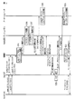
この発明の一実施形態に係る半導体装置について、図1を用いて説明する。図1は、本実施形態に係るメモリシステムのブロック図である。 A semiconductor device according to an embodiment of the present invention will be described with reference to FIG. FIG. 1 is a block diagram of a memory system according to this embodiment.
<メモリシステムの全体構成>
図示するように、本実施形態に係るメモリシステム1は、大まかにはNAND型フラッシュメモリ2、入出力部3、制御部4、及びデータバススイッチ5を備えている。そして、これらのNAND型フラッシュメモリ2、入出力部3、制御部4、及びデータバススイッチ5は、同一の半導体基板上に形成され、1つのチップに集積されている。以下、各ブロックの詳細について説明する。
<Overall configuration of memory system>
As shown in the figure, the
<NAND型フラッシュメモリ2>
NAND型フラッシュメモリ2は、メモリシステム1の主記憶部として機能する。図示するようにNAND型フラッシュメモリ2は、メモリセルアレイ10、ロウデコーダ11、センスアンプ12、ページバッファ13、カラムデコーダ14、電圧発生回路15、シーケンサ16、及びオシレータ17、18を備えている。
<NAND
The
メモリセルアレイ10は、データを保持可能な複数のメモリセルトランジスタを備えている。図2はメモリセルアレイ10の回路図であり、センスアンプ12及びページバッファ13を合わせて図示している。図示するようにメモリセルアレイ10は、大まかには第1領域10−1と第2領域10−2とを含む。第1領域10−1は、ユーザデータ等の正味のデータ(以下、メインデータと呼ぶ)を保持する。他方、第2領域10−2は第1領域10−1のスペア領域として用いられ、例えばエラー訂正用の情報(パリティ等)を保持する。
The
第1領域10−1及び第2領域10−2はそれぞれ、複数のメモリセルユニット50を備えている。メモリセルユニット50の各々は、例えば32個のメモリセルトランジスタMT(MT0〜MT31)と、選択トランジスタST1、ST2とを含んでいる。メモリセルトランジスタMTは、半導体基板上にゲート絶縁膜を介在して形成された電荷蓄積層(例えば浮遊ゲート)と、電荷蓄積層上にゲート間絶縁膜を介在して形成された制御ゲートとを有する積層ゲート構造を備えている。なお、メモリセルトランジスタMTの個数は32個に限られず、8個や16個、34個、128個、256個等であってもよく、その数は限定されるものではない。また、メモリセルトランジスタMTは、窒化膜に電子をトラップさせる方式を用いたMONOS(Metal Oxide Nitride Oxide Silicon)構造であっても良い。
Each of the first region 10-1 and the second region 10-2 includes a plurality of
メモリセルトランジスタMTは、隣接するもの同士でソース、ドレインを共有している。そして、選択トランジスタST1、ST2間に、その電流経路が直列接続されるようにして配置されている。直列接続されたメモリセルトランジスタMTの一端側のドレインは選択トランジスタST1のソースに接続され、他端側のソースは選択トランジスタST2のドレインに接続されている。 Adjacent ones of the memory cell transistors MT share a source and a drain. And it arrange | positions so that the current path may be connected in series between selection transistor ST1, ST2. The drain on one end side of the memory cell transistors MT connected in series is connected to the source of the select transistor ST1, and the source on the other end side is connected to the drain of the select transistor ST2.
同一行にあるメモリセルトランジスタMTの制御ゲートは、ワード線WL(WL0〜WL31)のいずれかに共通接続される。また同一行にある選択トランジスタST1、ST2のゲートは、それぞれセレクトゲート線SGD、SGSに共通接続されている。ワード線WL及びセレクトゲート線SGD、SGSは、第1領域10−1と第2領域10−2とで共通に用いられる。 The control gates of the memory cell transistors MT in the same row are commonly connected to one of the word lines WL (WL0 to WL31). The gates of the select transistors ST1 and ST2 in the same row are commonly connected to select gate lines SGD and SGS, respectively. The word line WL and the select gate lines SGD and SGS are used in common in the first region 10-1 and the second region 10-2.
第1領域10−1において同一列にある選択トランジスタST1のドレインは、ビット線BL(BL0〜BLn(nは自然数))に共通接続される。また、第2領域10−2において同一列にある選択トランジスタST1のドレインは、ビット線BL(BL(n+1)〜BLm(mは自然数))に共通接続される。選択トランジスタST2のソースはソース線SLに共通接続される。 The drains of the select transistors ST1 in the same column in the first region 10-1 are commonly connected to the bit lines BL (BL0 to BLn (n is a natural number)). Further, the drains of the selection transistors ST1 in the same column in the second region 10-2 are commonly connected to the bit lines BL (BL (n + 1) to BLm (m is a natural number)). The sources of the selection transistors ST2 are commonly connected to the source line SL.
上記構成において、同一のワード線WLに接続された複数のメモリセルトランジスタMTには一括してデータが書き込まれ、または読み出され、この単位をページと呼ぶ。更に、同一行にある複数のメモリセルユニット40は一括してデータが消去され、この単位をメモリブロックと呼ぶ。
In the above configuration, data is written or read all at once to a plurality of memory cell transistors MT connected to the same word line WL, and this unit is called a page. Further, data is erased collectively from a plurality of
センスアンプ12及びページバッファ13は、ページサイズのデータを保持可能なバッファメモリであり、NAND型フラッシュメモリ1における1次データキャッシュ及び2次データキャッシュとしてそれぞれ機能する。
The
センスアンプ12は、データの読み出し時には、メモリセルアレイ10から読み出されたデータをセンス・増幅して一時的に保持し、ページバッファ13へ転送する。また書き込み時には、ページバッファ13から転送されたデータをビット線BLに転送して、データのプログラムを実行する。
At the time of reading data, the sense amplifier 12 senses and amplifies data read from the
ページバッファ13は、NANDデータバス6、及びユーザデータバス7またはECCデータバス8を介して入出力部3に接続される。そしてデータの読み出し時には、センスアンプ12から転送されたデータを入出力部3へ出力する。また書き込み時には、入出力部3から入力されたデータを一時的に保持し、これをセンスアンプ12に転送する。
The
センスアンプ12及びページバッファ13は、例えばビット線BL毎に設けられたラッチ回路を備え、これにより1ページ分のデータを保持出来る。従って、図2に示すように、一部の領域がメインデータ保持用として使用され、残りがパリティ等のECCデータ保持用として使用される。なお、ラッチ回路は1ページ分だけあれば良い。よって、例えば偶数ビット線毎、及び奇数ビット線毎にデータのプログラム及び読み出しが行われる場合には、全ビット線に対して一括してデータのプログラム及び読み出しが行われる場合に比べて、ページサイズは半分となる。よって必要なラッチ回路数も半分となる。ページサイズは、例えば4Kバイトである。
The
図1に戻って説明を続ける。ロウデコーダ11は、メモリセルアレイ10におけるいずれかのページ(すなわちワード線WL)を選択する。カラムデコーダ14は、メモリセルアレイ10におけるいずれかのカラム(すなわちビット線BL)を選択する。
Returning to FIG. 1, the description will be continued. The
電圧発生回路15は、外部から与えられる電圧を昇圧または降圧することにより、データのプログラム、読み出し、及び消去に必要な電圧を発生する。そして発生した電圧を、例えばロウデコーダ11に供給する。電圧発生回路15で発生された電圧が、ワード線WLに印加される。
The
シーケンサ16は、NAND型フラッシュメモリ2全体の動作を司る。すなわち、制御部4から命令(NAND I/F Command)を受けると、これに応答して、データのプログラム、読み出し、及び消去を実行するためのシーケンスを実行する。そして、このシーケンスに従って、電圧発生回路15、センスアンプ12、及びページバッファ13等の動作を制御する。
The
オシレータ17は内部クロックICLKを生成する。すなわち、クロック生成器として機能する。そしてオシレータ17は、生成した内部クロックICLKをシーケンサ16に供給する。シーケンサ16は、この内部クロックICLKに同期して動作する。
The
オシレータ18は内部クロックACLKを生成する。すなわち、クロック生成器として機能する。そしてオシレータ18は、生成した内部クロックACLKを、制御部4や入出力部3へ供給する。内部クロックACLKは、制御部4や入出力部3の動作の基準となるクロックである。
The
<データバススイッチ5>
データバススイッチ5は、入出力部3の命令に従って、NANDデータバス6を、ユーザデータバス7またはECCデータバス8に接続する。例えばデータバススイッチ5は、通常時はNANDデータバス6をユーザデータバス7に接続する。そして必要に応じてNANDデータバス6をECCデータバス8に接続する。またNANDデータバス6、ユーザデータバス7、及びECCデータバス8は例えば同じバス幅を有し、そのバス幅は例えば4バイトである。
<
The
<入出力部3>
次に、引き続き図1を参照しつつ、入出力部3について説明する。入出力部3は、パイプラインバッファ21、バーストバッファ(burst buffer)22、ユーザインターフェース23、アクセスコントローラ24、デコーダ25、及びECC部30を備えている。
<Input / output unit 3>
Next, the input / output unit 3 will be described with reference to FIG. The input / output unit 3 includes a
なお、本実施形態に係るメモリシステム1では、NAND型フラッシュメモリ2が主記憶部として機能し、NAND型フラッシュメモリ2に対するデータの入出力を、入出力部3が司る。従って、NAND型フラッシュメモリ2からデータを外部に読み出す際には、まずNAND型フラッシュメモリ2のメモリセルアレイ10から読み出されたデータが、ページバッファ12に格納される。その後、ユーザの要求に応じて、ページバッファ13内のデータがユーザインターフェース23を介して外部に出力される。他方、データをNAND型フラッシュメモリ2に記憶させる際には、まず外部から与えられたデータが、ユーザインターフェース23を介してページバッファ13に格納される。その後、ページバッファ13内のデータがメモリセルアレイ10に書き込まれる。
In the
以下では、データがメモリセルアレイ10からページバッファ13に読み出されるまでの動作を、データの“ロード(load)”と呼ぶ。また、ページバッファ13内のデータが、ユーザインターフェース23に転送されるまでの動作を、データの“リード(read)”と呼ぶ。
Hereinafter, an operation until data is read from the
更に、NAND型フラッシュメモリ2に記憶させるべきデータが、ユーザインターフェース23からページバッファ13に転送されるまでの動作を、データの“ライト(write)”と呼ぶ。また、ページバッファ13内のデータがメモリセルアレイ10に書き込まれるまでの動作を、データの“プログラム(program)”と呼ぶ。
Furthermore, an operation until data to be stored in the
入出力部3の説明に戻る。
ECC部30は、NAND型フラッシュメモリ2に対する入出力データについてのエラー検出及びエラー訂正、並びにパリティの生成(以下、これらをまとめてECC処理と呼ぶことがある)を実行する。ECC部30は、ECCバッファ31、ECCデコーダ32、ECC解析部33、及びECC制御部34を備えている。
Returning to the description of the input / output unit 3.
The
ECCバッファ21は、ECCデータバス8に接続されている。そして、ECCデータバス8及びNANDデータバス6を介して、NAND型フラッシュメモリ2のページバッファ13と接続される。そして、ページバッファ13からNANDデータバス6及びECCデータバス8を介してデータを読み出し、これをECC解析部33に転送する。またECCバッファ31は、ECCデコーダ32によってエラー訂正されたデータ、及びECC解析部33で発生されたパリティを一時的に保持し、これをECCデータバス8及びNANDデータバス6を介してページバッファ13に書き込む。ECCバッファ31のサイズは、例えばECCデータバス8のバス幅と同じサイズであり、例えば4バイトである。しかし、ECCデータバス28のバス幅より大きくても良い。
The
ECC解析部33は、データのロード時には、ECCバッファ31から転送されたデータを用いてECC処理を行い、該データにおけるエラーの有無を判断する。またデータのプログラム時には、ECCバッファ31から転送されたデータに基づいて、パリティを生成する。
When the data is loaded, the
ECCデコーダ32は、データのロード時には、ECC解析部33においてエラーが有ると判断された場合、その位置を特定すると共に、対応するデータをページバッファ13からECCバッファ31に読み出し、データを訂正する。またデータのプログラム時には、ECC解析部33で生成されたパリティをECCバッファ31に保持させ、これをページバッファ13に転送させる。
When the
ECC制御部34は、ECC解析部33を制御する。
The
次にユーザインターフェース23について説明する。ユーザインターフェース23は、メモリシステム1外部のホスト機器(ユーザ)と接続可能とされ、ホスト機器との間でデータ、制御信号、及びアドレスAdd等、種々の信号の入出力を司る。制御信号の一例は、メモリシステム1全体をイネーブルにするチップイネーブル信号/CE、アドレスをラッチさせるためのアドレスバリッド信号/AVD、バーストリード(burst read)用のクロックCLK、書き込み動作をイネーブルにするライトイネーブル信号/WE、データの外部への出力をイネーブルにするアウトプットイネーブル信号/OE、などである。
Next, the
ユーザインターフェース23は、データ入出力バスによりバーストバッファ22と接続されている。データ入出力バスは、例えば2バイトである。そしてユーザインターフェース23は、ホスト機器からのデータのリード要求、ロード要求、及びプログラム要求等に係る制御信号をアクセスコントローラ50へ転送する。そしてデータリード時には、バーストバッファ22内のデータをホスト機器へ出力する。またデータライト時には、ホスト機器から与えられるデータをバーストバッファ22へ転送する。
The
バーストバッファ22は、バッファ/レジスタデータバスにより、パイプラインバッファ21及び制御部4とデータ転送可能とされている。バッファ/レジスタデータバスのバス幅は、例えばユーザデータバス7と同じである。そして、ホスト機器からユーザインターフェース23を介して与えられるデータ、またはパイプラインバッファ21から与えられるデータを、一時的に保持する。
The
パイプラインバッファ21は、ユーザデータバス7及びバッファ/レジスタデータバスと接続されている。そしてデータライト時には、バーストバッファ22から転送されるデータを一時的に保持する。そして、ユーザデータバス7及びNANDデータバス6を介して、データをページバッファ13に書き込む。またデータリード時には、ユーザデータバス7及びNANDデータバス6を介して、ページバッファ13からデータを読み出し、これをバーストバッファ22へ転送する。
The
次にアクセスコントローラ24について説明する。アクセスコントローラ24は、ユーザインターフェース23から制御信号及びアドレスを受け取る。そして、ホスト機器の要求を満たす動作を実行するよう、パイプラインバッファ21、データバススイッチ5、バーストバッファ22、デコーダ25、及び制御部4を制御する。
Next, the
例えば、ホスト機器の要求に応じてアクセスコントローラ24は、制御部4における後述するレジスタ40をアクティブ状態として、レジスタにコマンド(Write/Read)をセットする。また、パイプラインバッファ21に対して、ページバッファ13またはバーストバッファ22からデータを読み出すよう命令する。更にデコーダ25に対して、外部から入力されたアドレスを転送する。
For example, in response to a request from the host device, the
デコーダ25は、アクセスコントローラ24から与えられたアドレス(カラムアドレス)をデコードする。そしてデコード結果に応じて、NAND型フラッシュメモリ2のカラムデコーダ14を制御して、ページバッファ13における所定のアドレスに対応するデータを出力させる。
The
<制御部4>
次に、引き続き図1を参照しつつ、制御部4について説明する。制御部4は、NAND型フラッシュメモリ2及び入出力部3の動作を制御する。すなわち、メモリシステム1全体としての動作を統括する機能を有する。図示するように制御部4は、レジスタ40、コマンドユーザインターフェース(command user interface)41、ステートマシン(state machine)42、NANDアドレス/コマンド発生回路43、及びバッファアドレス/タイミング発生回路44を備えている。
<
Next, the
レジスタ40は、ファンクションの動作状態を設定するためのレジスタである。すなわちレジスタ40は、アクセスコントローラ24から与えられるコマンドに応じて、ファンクションの動作状態を設定する。より具体的には、レジスタ40には、例えばデータロード時にはロードコマンドが設定され、データプログラム時にはプログラムコマンドが設定される。
The
コマンドユーザインターフェース41は、所定のコマンドがレジスタ40に設定されることで、メモリシステム1に対してファンクション実行コマンドが与えられたことを認識する。そして、内部コマンド信号(Command)を発行し、ステートマシン42へ出力する。
The
ステートマシン42は、コマンドユーザインターフェース41から与えられる内部コマンド信号に基づいて、メモリシステム1内部におけるシーケンス動作を制御する。ステートマシン42がサポートするファンクションは、ロード、プログラム、及び消去等、多数あり、これらのファンクションを実行するよう、NAND型フラッシュメモリ2及び入出力部3の動作を制御する。ステートマシン42は、オシレータ18の生成する内部クロックACLKに同期しつつ、これらの制御を行う。またステートマシン42は、NANDシーケンサ16から与えられるレディ信号及びエラー信号により、NAND型フラッシュメモリ2の動作状態を把握出来る。
The
NANDアドレス/コマンド発生回路43は、ステートマシン42の制御に基づいてNAND型フラッシュメモリ2の動作を制御する。より具体的には、アドレスや、NANDインターフェースにサポートされたコマンド(Program/Load)等を生成し、NAND型フラッシュメモリ2へ出力する。
The NAND address /
バッファアドレス/タイミング発生回路44は、ステートマシン42の制御に基づいて入出力部3の動作を制御する。より具体的には、入出力部3において必要なアドレスやコマンドを発行して、アクセスコントローラ24及びECC制御部34へ出力する。
The buffer address /
<メモリシステム1のデータ読み出し動作>
次に、上記構成のメモリシステム1におけるデータの読み出し動作について、図3を用いて説明する。図3はメモリシステム1の動作の流れを示すフローチャートである。
<Data read operation of
Next, a data read operation in the
図示するように、まずユーザインターフェース23が、ホスト機器を介してユーザから入力されたアドレスを受け付ける(ステップS10)。このアドレスは、NAND型フラッシュメモリ2におけるメモリセルアレイ10のページアドレスである。このページアドレスは、ユーザインターフェース23からアクセスコントローラ24に転送される。するとアクセスコントローラ24は、制御部3のレジスタ40をアクティブとし、このページアドレスを転送する(ステップS11)。
As shown in the figure, first, the
引き続きユーザインターフェース23は、ホスト機器から入力されたロードコマンドを受け付ける(ステップS12)。すると、ロードコマンドを受信したアクセスコントローラ24は、ロードコマンドをレジスタ40にセットする(ステップS13)。
Subsequently, the
レジスタ40にコマンドがセットされると、コマンドユーザインターフェース41はこれを検知し、内部コマンド信号を生成する。ここではロードコマンドが成立する(ステップS14)。そしてロードコマンドの成立を受けて、ステートマシン42が起動する。
When a command is set in the
ステートマシン42は、各回路ブロックについて必要な初期化を行った後、NANDアドレス/コマンド発生回路43に対して、NAND型フラッシュメモリ2に対してセンスコマンドを発行するよう要求する。するとNANDアドレス/コマンド発生回路43は、レジスタ40に設定されたアドレスについてデータのセンスを行うよう、シーケンサ16に対してセンスコマンドを発行する(ステップS15)。
After performing necessary initialization for each circuit block, the
NANDアドレス/コマンド発生回路43からセンスコマンドを受けることで、NAND型フラッシュメモリ2ではシーケンサ16が起動する(ステップS16)。シーケンサ16は、NAND型フラッシュメモリ2において必要な回路の初期化を行った後、指定されたアドレスのセンス動作を行う。すなわち、電圧発生回路15、ロウデコーダ11、カラムデコーダ14、センスアンプ12、及びページバッファ13を制御し、センスデータをページバッファ13に格納させる(ステップS17)。より具体的には、メモリセルアレイ10内のあるページからデータが読み出され、読み出しデータをセンス・増幅した結果がページバッファ13に格納される。その後シーケンサ16は、センス動作が終了したことを、ステートマシン42に通知する(ステップS18)。
By receiving the sense command from the NAND address /
更にステートマシン42は、バッファアドレス/タイミング発生回路44及びアクセスコントローラ24を介して、データバススイッチ5に対して、NANDデータバス6をECCデータバス8に接続するよう命令する(ステップS19)。この命令に応答してデータバススイッチ5は、NANDデータバス6をユーザデータバス7から切り離し、新たにECCデータバス8に接続する(ステップS20)。
Further, the
更にステートマシン42は、NANDアドレス/コマンド発生回路43に対して、リードコマンドを発行するよう命令する。この命令に応答してNANDアドレス/コマンド発生回路43は、シーケンサ16に対して、NANDインターフェースでサポートされたリードコマンドを発行する(ステップS21)。このリードコマンドを受けてシーケンサ16は、ページバッファ13をリード可能にセットする。
Further, the
そして、ステートマシン42がリードコマンド(クロック)をシーケンサ16に対して発行する(ステップS22)。これにより、ページバッファ13内のデータが、NANDデータバス6及びECCデータバス8を介してECCバッファ31に読み出される(ステップS23)。
Then, the
引き続きステートマシン42は、バッファアドレス/タイミング発生回路44を介して、ECC制御部34に対してECC訂正開始命令を発行する(ステップS24)。この命令に応答してECC部30は、エラー検出及びエラー訂正を行う(ステップS25)。すなわち、ECC制御部34による制御に従い、ECC解析部33はECCバッファ31に読み出されたデータにつきシンドロームを生成する。そしてこのシンドロームを元にして、ECCデコーダ32がデータの誤り位置を決定する。そしてECCデコーダ32はエラーを訂正して、訂正後のデータをページバッファ13に格納する(ステップS26)。
Subsequently, the
ECC処理の後、ステートマシン42の命令に応答して(ステップS27)、データバススイッチ5は、NANDデータバス6をECCデータバス8から切り離し、ユーザデータバス7に接続する(ステップS28)。そして制御部4では、ユーザがモニタするためのステータスなどをセットする(ステップS29)。
After the ECC processing, in response to an instruction from the state machine 42 (step S27), the
その後、ホスト機器からアドレス(言い換えればリード要求)が入力されると(ステップS30)、ページバッファ13内のデータが外部へ出力される(ステップS31)。このアドレスは、ページバッファ内における任意の領域を指定するアドレス(ページバッファアドレス)である。ユーザインターフェース23に入力されたページバッファアドレスは、アクセスコントローラ24を介してデコーダ25に与えられる。するとデコーダ25はこれをデコードし、ページバッファ内の対応するアドレスのデータを選択するよう、カラムデコーダ14に(またはページバッファに直接)命令する。その結果、当該アドレスのデータが、NANDデータバス6及びユーザデータバス7を介してパイプラインバッファ21に読み出され、バーストバッファ22及びユーザインターフェース23を介してホスト機器へ出力される。
Thereafter, when an address (in other words, a read request) is input from the host device (step S30), the data in the
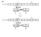
<ECC部30の動作について>
次に、上記データの読み出し時におけるステップS23〜S26の詳細について図4及び図5を用いて説明する。図4は、ステップS23〜S26の詳細を示すフローチャートである。また図5は、ページバッファ13からECCバッファ31に転送されるデータ、ECC解析部33及びECCデコーダ32の動作、並びにECCバッファ31からページバッファ13に転送されるデータを示すタイムチャートである。
<Operation of the
Next, details of steps S23 to S26 at the time of reading the data will be described with reference to FIGS. FIG. 4 is a flowchart showing details of steps S23 to S26. FIG. 5 is a time chart showing data transferred from the
図示するように、ページバッファ13のデータが、ECCデータバス8のバス幅単位(例えば4バイト単位)で、ECCバッファ31に転送される(ステップS40)。転送されるデータには、メインデータだけでなくECCデータも含まれる。通常、ページバッファ13のサイズはECCデータバス8のバス幅よりも大きい。従って、ステップS40を複数回、繰り返すことで、ページバッファ13内の全データがECCバッファ31に転送される(ステップS41、NO、ステップS40)。これが図5の時刻t1〜t2の期間である。図5の例では、k回(kは2以上の自然数)のデータ転送により、ページバッファ13内のメインデータの全てがECCバッファ31に転送される例を示している。なお、i回目(iは2〜kのいずれかをとる変数)に転送されるメインデータをデータDiと呼ぶ。つまりデータDiは4バイトである。また図5のDpはECCデータ(パリティ)を示す。図6の例では1回の転送でパリティDpが転送される場合を示しているが、複数回の転送により行っても良い。ECCバッファ31は、データを受信する度に、これをECC解析部33に転送する。なお、前述の通りECCバッファ31は、例えばECCデータバス8のバス幅と同程度の容量である。よってこの場合には、ページバッファ13からデータが転送される度に、ECCバッファ31は、新たなデータをそれまで保持していたデータに上書きする。
As shown in the drawing, the data in the
ページバッファ13内の全データの転送が完了すると(ステップS41、YES)、ステートマシン42からのECC訂正開始命令に応答して、ECC解析部33がエラーの有無を判断する(ステップS42、図5の時刻t2〜t3)。すなわち、ステップS40で受信したデータに基づいてシンドロームを生成する。
When the transfer of all the data in the
エラーが無ければ(ステップS43、NO)、処理は終了する。エラーが有れば(ステップS43、YES)、次にECCデコーダ32において、エラーのあるデータとその位置を判断する(ステップS44、図5の時刻t3〜t4)。例えば、データD2にエラーがあったと仮定する。するとECCデコーダ32は、データD2のアドレス(ページバッファ13内のアドレス)と、エラーのあるビット位置、及びそのエラーの内容を算出する。
If there is no error (step S43, NO), the process ends. If there is an error (step S43, YES), the
そしてECCデコーダ32の命令により、ECCバッファ31はデータD2をページバッファ13から読み出す(ステップS45、図5の時刻t4〜t5)。その他のデータD1、D3〜Dk、Dpは読み出されない。この様子を図6の上図に示す。図示するように、データD2のあるビットに誤りがあり、“0”が“1”に反転していたとする。するとこのデータD2のみがECCバッファ31に読み出される。
Then, according to the instruction of the
次に、ECCデコーダ32がエラーの訂正を行う(ステップS46、図5の時刻t5〜t6)。すなわち、図6の下図に示すようにECCデコーダ32は、ECCバッファ31内のデータD2における誤りビットを、“1”から“0”に反転させる。その後、ECCバッファ31は、エラーの訂正されたデータD2を、ページバッファ13のデータD2に上書きする(ステップS47、図5の時刻t6)。
Next, the
<メモリシステム1のデータ書き込み動作>
次に、データの書き込み動作について、図7を用いて説明する。図7はメモリシステム1の動作の流れを示すフローチャートである。
<Data Write Operation of
Next, a data write operation will be described with reference to FIG. FIG. 7 is a flowchart showing an operation flow of the
図示するように、まずユーザインターフェース23が、ホスト機器を介してユーザから入力された、プログラムすべきデータを受け付ける(ステップS50)。このデータは、バーストバッファ22、パイプラインバッファ21、ユーザデータバス7、及びNANDデータバス6を介してページバッファ13に格納される(ステップS51)。
As shown in the drawing, first, the
その後、ユーザインターフェース23は、ホスト機器を介してユーザから入力されたアドレスを受け付ける(ステップS52)。このアドレスは、NAND型フラッシュメモリ2におけるメモリセルアレイ10のページアドレスである。このページアドレスは、ユーザインターフェース23からアクセスコントローラ24に転送される。するとアクセスコントローラ24は、制御部3のレジスタ40をアクティブとし、このページアドレスを転送する(ステップS53)。
Thereafter, the
引き続きユーザインターフェース23は、ホスト機器から入力されたプログラムコマンドを受け付ける(ステップS54)。すると、プログラムコマンドを受信したアクセスコントローラ24は、プログラムコマンドをレジスタ40にセットする(ステップS55)。
Subsequently, the
レジスタ40にコマンドがセットされると、コマンドユーザインターフェース41はこれを検知し、内部コマンド信号を生成する。ここではプログラムコマンドが成立する(ステップS56)。そしてプログラムコマンドの成立を受けて、ステートマシン42が起動する。
When a command is set in the
ステートマシン42は、各回路ブロックについて必要な初期化を行った後、NANDアドレス/コマンド発生回路43に対して、NAND型フラッシュメモリ2に対してリードコマンドを発行するよう要求する。するとNANDアドレス/コマンド発生回路43は、シーケンサ16に対してリードコマンドを発行する(ステップS57)。このリードコマンドを受けてシーケンサ16は、ページバッファ13をリード可能にセットする。
After performing necessary initialization for each circuit block, the
引き続きステートマシン42は、バッファアドレス/タイミング発生回路44及びアクセスコントローラ24を介して、データバススイッチ5に対して、NANDデータバス6をECCデータバス8に接続するよう命令する(ステップS58)。この命令に応答してデータバススイッチ5は、NANDデータバス6をユーザデータバス7から切り離し、新たにECCデータバス8に接続する(ステップS59)。
Subsequently, the
そして、ステートマシン42がリードコマンド(クロック)をページバッファ13に対して発行する(ステップS60)。これにより、ページバッファ13内のデータが、NANDデータバス6及びECCデータバス8を介してECCバッファ31に読み出される(ステップS61)。
Then, the
引き続きステートマシン42は、バッファアドレス/タイミング発生回路44を介して、ECC制御部34に対してパリティ発生開始命令を発行する(ステップS62)。この命令に応答してECC部30はパリティの生成を開始する(ステップS63)。すなわち、ECC制御部34による制御に従い、ECC解析部33はECCバッファ31に読み出されたデータにつきシンドロームを生成し、このシンドロームを元にしてパリティを生成する。そしてECCデコーダ32を介して、生成したパリティをECCバッファ31に格納し、これをページバッファ13に転送する(ステップS64)。
Subsequently, the
その後、ステートマシン42は、NANDアドレス/コマンド発生回路43に対して、NAND型フラッシュメモリ2に対してプログラムコマンドを発行するよう要求する。すると、NANDアドレス/コマンド発生回路43はシーケンサ16に対して、ページバッファ13内のデータを、レジスタ40内のアドレス(ページアドレス)にプログラムするよう、プログラムコマンドを発行する(ステップS65)。
Thereafter, the
このプログラムコマンドを受けてシーケンサ16は、NAND型フラッシュメモリ2において必要な回路の初期化を行った後、プログラム動作を行う(ステップS66)。すなわち、電圧発生回路15、ロウデコーダ11、カラムデコーダ14、センスアンプ12、及びページバッファ13を制御し、ページバッファ13内のデータを所定のページにプログラムする。
In response to the program command, the
更にステートマシン42は、バッファアドレス/タイミング発生回路44及びアクセスコントローラ24を介して、データバススイッチ5に対して、NANDデータバス6をユーザデータバス7に接続するよう命令する(ステップS67)。この命令に応答してデータバススイッチ5は、NANDデータバス6をECCデータバス8から切り離し、新たにユーザデータバス7に接続する(ステップS68)。
Further, the
NAND型フラッシュメモリ2においてプログラムが完了すると、その旨をシーケンサ16がステートマシン42に通知する(ステップS69)。その後、制御部4では、ユーザがモニタするためのステータスなどをセットする(ステップS70)。
When the program is completed in the
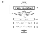
<ECC部30の動作について>
次に、上記データの書き込み時におけるステップS61〜S64の詳細について図8及び図9を用いて説明する。図8は、ステップS61〜S64の詳細を示すフローチャートである。また図9は、ページバッファ13からECCバッファ31に転送されるデータ、ECC解析部33の動作、ECC解析部33からECCバッファ31に転送されるデータ、及びECCバッファ31からページバッファ13に転送されるデータを示すタイムチャートである。
<Operation of the
Next, details of steps S61 to S64 when the data is written will be described with reference to FIGS. FIG. 8 is a flowchart showing details of steps S61 to S64. 9 shows data transferred from the
図示するように、読み出し時と同様に、ページバッファ内の全てのデータがECCバッファ31に転送される(ステップS40、S41、図9の時刻t1〜t2)。当然ながら、書き込み時にECCバッファ31に転送されるデータはプログラムすべきメインデータである。パリティはこれから生成される。
As shown, all data in the page buffer is transferred to the ECC buffer 31 (steps S40 and S41, times t1 to t2 in FIG. 9), as in reading. Of course, the data transferred to the
ページバッファ13内の全データの転送が完了すると(ステップS41、YES)、ステートマシン42からのパリティ発生開始命令に応答してECC解析部33が、ステップS40で受信したデータに基づいてシンドロームを生成し、これに基づきパリティを生成する(ステップS80、図9の時刻t2〜t3)。
When the transfer of all data in the
そしてECC解析部33は、生成したパリティDpをECCバッファへ転送し(ステップS81、図9の時刻t3〜t4)、更にページバッファ13へ転送する(ステップS82、図9の時刻t4)。
The
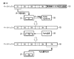
以上の様子を図10に模式的に示す。図10は、ページバッファ13と、ECC部30の一部を示すブロック図であり、時間の流れと共にデータの転送の様子を順次示している。図示するように、まずデータD1〜Dkが順次、ECCバッファ31に転送され、更にECC解析部33に転送される。読み出し時と同様に、データの転送はECCデータバス8のバス幅で行われる。よって、k回の転送により、全データがECCバッファ31に転送される。
The above situation is schematically shown in FIG. FIG. 10 is a block diagram showing a part of the
次に、ECC解析部33においてパリティが生成される。このパリティDpは、ECCバッファ31に転送される(上書きされる)。
Next, a parity is generated in the
その後、ECCバッファ31は、パリティDpをページバッファ13に格納する。パリティDpが格納される領域は、図2で説明したメモリセルアレイ10の第2領域10−2に対応する領域である。
Thereafter, the
<効果>
以上のように、この発明の実施形態に係る構成であると、NAND型フラッシュメモリを備えた半導体装置の回路面積を削減出来る。本効果につき、以下説明する。
<Effect>
As described above, the configuration according to the embodiment of the present invention can reduce the circuit area of the semiconductor device including the NAND flash memory. This effect will be described below.
本実施形態に係る構成であると、入出力部3は、ユーザデータバス7とECCデータバス8を含む2系統のデータバスを備えている。ユーザデータバス7は、外部のホスト機器と送受信を行うユーザインターフェース23に接続されたバスであり、ECCデータバス8はECC部30に接続されたバスである。更に、入出力部3はデータバススイッチ6を備え、NANDデータバス6と、ユーザデータバス7及びECCデータバス8との接続を切り替えている。
In the configuration according to the present embodiment, the input / output unit 3 includes two systems of data buses including a
より具体的には、データをNAND型フラッシュメモリ2に書き込む際には、まずデータバススイッチ5によってNANDデータバス6とユーザデータバス7とを接続して、書き込みデータをページバッファ13に格納する。その後、データバススイッチ5によりNANDデータバス6とECCデータバス8とを接続して、書き込みデータをECCバッファ31に読み出してパリティを生成し、これをページバッファ13に書き込む。
More specifically, when writing data into the
他方、データをNAND型フラッシュメモリ2から読み出す際には、まずデータバススイッチ5によってNANDデータバス6とECCデータバス8とを接続して、メインデータをページバッファ13からECCバッファ31に読み出し、エラー訂正を行い、訂正後のデータをページバッファ13に上書きする。その後、データバススイッチ5によりNANDデータバス6とユーザデータバス7とを接続して、読み出しデータを外部に出力する。
On the other hand, when reading data from the
以上のような構成とすることで、NAND型フラッシュメモリ2のページバッファ13を、メモリシステム1におけるバッファメモリとして使用している。従って、従来の例えばSRAMのようなバッファメモリが不要となる。従って、回路面積を大幅に削減出来る。
With the configuration as described above, the
特に、従来のSRAMとNAND型フラッシュメモリとを備えた構成と比べた場合、次のような差異がある。すなわち、従来型の構成であると、ECCバッファはデータバスによりSRAMバッファへ接続されるため、ページバッファ、ECCバッファ、及びSRAMバッファが直列接続される。これに対して本実施形態に係る構成であると、ECCバッファ31から他のバッファへ直接接続するデータバスは不要であり、データバススイッチ5により、ECCバッファ31はパイプラインバッファ21と並列的に接続される。言い換えれば、ECCデータバス8は、外部と接続するためのユーザデータバス7と並列的に接続される。
In particular, when compared with a configuration including a conventional SRAM and a NAND flash memory, there are the following differences. That is, in the conventional configuration, since the ECC buffer is connected to the SRAM buffer by the data bus, the page buffer, the ECC buffer, and the SRAM buffer are connected in series. On the other hand, in the configuration according to the present embodiment, a data bus directly connected from the
これにより、ユーザはページバッファ13に対して直接、読み出し及び書き込みを行うことが出来る。そのため、ページバッファ13はメモリシステム1のバッファメモリとしての役割を果たすことが出来る。
As a result, the user can directly read from and write to the
また、入出力部25はデコーダ25を備えており、これによりページバッファ13にアクセス出来る。つまり、NAND型フラッシュメモリ2においてシーケンサ16によって制御される内部動作とは別系統で、ページバッファ13にアクセス出来る。従ってユーザは、ページバッファ13に対してランダムにアクセス(読み出し・書き込み)することが出来る。
In addition, the input /
なお、本実施形態に係る構成であると、ECC処理を行うためには、ページバッファ13にデータを格納した後に、改めてECCバッファ31にデータを読み出す必要がある。しかしながら、SRAMを排したことで、SRAMバッファとページバッファ間のデータ転送が不要となるため、ECC処理を含めてデータ転送時間が長くなることを抑制することも可能である。
Note that with the configuration according to the present embodiment, in order to perform ECC processing, it is necessary to read data into the
なお、上記実施形態ではNAND型フラッシュメモリが2段のキャッシュメモリ(センスアンプ12(Primary Data Cashe)及びページバッファ13(Secondary Data Cashe))を備える場合を例に説明した。しかし、1段だけの場合であっても良い。この場合には、NANDデータバス6はセンスアンプ12に接続される。
In the above-described embodiment, the NAND flash memory has been described as an example in which the two-stage cache memory (the sense amplifier 12 (Primary Data Cashe) and the page buffer 13 (Secondary Data Cashe)) is provided. However, it may be only one stage. In this case, the
また、2段のキャッシュメモリを有する構成においても、NANDデータバス6がページバッファ13ではなくセンスアンプ12に接続されても良い。この場合、センスアンプ12がバッファメモリとしての機能を果たす。
Also in a configuration having a two-stage cache memory, the
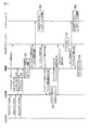
更に、2系統のNANDデータバス6を設けて、一方をページバッファ13に接続し、他方をセンスアンプ12に接続するようにしても良い。このような構成例を図11に示す。図11は、上記実施形態の変形例に係るメモリシステム1のブロック図であり、メモリシステム1の一部領域のみを示している。図示するように、2本のNANDデータバス6−1、6−2が設けられる。NANDデータバス6−1はページバッファ13に接続され、NANDデータバス6−2はセンスアンプ12に接続される。これらのNANDデータバス6−1、6−2がユーザデータバス7とECCデータバス8のいずれに接続されるかは、データバススイッチ5によって決定される。例えば、あるタイミングにおいては、一方がユーザデータバス7に接続され、他方ECCデータバス8に接続されてもよい。このような構成によれば、メモリシステム1の動作の更なる高速化を図ることが出来る。
Further, two
更に、上記実施形態では、NAND型フラッシュメモリ2、入出力部3、制御部4、及びデータバススイッチ5がワンチップに集積された例を挙げて説明した。このようなメモリシステム2の具体例としては、「OneNAND(登録商標)」型のフラッシュメモリが挙げられる。しかし、必ずしもワンチップ化されている場合に限らず、NAND型フラッシュメモリ2、入出力部3、制御部4、及びデータバススイッチ5が別々の半導体チップで実現されている場合であっても良い。更に上記実施形態では主記憶としてNAND型フラッシュメモリが用いられる場合を例に説明したが、NAND型フラッシュメモリに限らず、その他のフラッシュメモリであっても良く、更には強誘電体メモリや抵抗変化型メモリ(ReRAM)等のその他の半導体メモリであっても良い。
Furthermore, in the above embodiment, the
なお、本願発明は上記実施形態に限定されるものではなく、実施段階ではその要旨を逸脱しない範囲で種々に変形することが可能である。更に、上記実施形態には種々の段階の発明が含まれており、開示される複数の構成要件における適宜な組み合わせにより種々の発明が抽出されうる。例えば、実施形態に示される全構成要件からいくつかの構成要件が削除されても、発明が解決しようとする課題の欄で述べた課題が解決でき、発明の効果の欄で述べられている効果が得られる場合には、この構成要件が削除された構成が発明として抽出されうる。 Note that the present invention is not limited to the above-described embodiment, and various modifications can be made without departing from the scope of the invention in the implementation stage. Furthermore, the above embodiments include inventions at various stages, and various inventions can be extracted by appropriately combining a plurality of disclosed constituent elements. For example, even if some constituent requirements are deleted from all the constituent requirements shown in the embodiment, the problem described in the column of the problem to be solved by the invention can be solved, and the effect described in the column of the effect of the invention Can be extracted as an invention.
1…メモリシステム、2…NAND型フラッシュメモリ、3…入出力部、4…制御部、5…データバススイッチ、6…NANDデータバス、7…ユーザデータバス、8…ECCデータバス、10…メモリセルアレイ、11…ロウデコーダ、12…センスアンプ、13…ページバッファ、14…カラムデコーダ、15…電圧発生回路、16…シーケンサ、17、18…オシレータ、21…パイプラインバッファ、22…バーストバッファ、23…ユーザインターフェース、24…アクセスコントローラ、25…デコーダ、30…ECC部、31…ECCバッファ、32…ECCデコーダ、33…ECC解析部、34…ECC制御部、40…レジスタ、41…コマンドユーザインターフェース、42…ステートマシン、43…NANDアドレス/コマンド発生回路、44…バッファアドレス/タイミング発生回路、50…メモリセルユニット
DESCRIPTION OF
Claims (5)
前記NAND型フラッシュメモリに入力されるデータ、またはNAND型フラッシュメモリから出力されるデータについてECC処理を行うECC部と、外部との間でデータの授受を行うインターフェースとを有し、前記NAND型フラッシュメモリと外部との間のデータの入出力を司る入出力部と、
前記NAND型フラッシュメモリと前記ECC部との間の接続と、前記NAND型フラッシュメモリと前記インターフェースとの間の接続とを切り替えるスイッチと、
前記NAND型フラッシュメモリ、前記入出力部、及びスイッチを制御する制御部と
を具備することを特徴とする半導体装置。 NAND flash memory,
An ECC unit that performs ECC processing on data input to the NAND flash memory or data output from the NAND flash memory, and an interface that exchanges data with the outside, and the NAND flash An input / output unit that controls input / output of data between the memory and the outside;
A switch for switching a connection between the NAND flash memory and the ECC unit and a connection between the NAND flash memory and the interface;
A semiconductor device comprising: the NAND flash memory; the input / output unit; and a control unit that controls a switch.
前記入出力部は、外部から入力されたアドレスをデコードして、前記メモリセルアレイの前記カラムを選択可能なデコーダを更に備える
ことを特徴とする請求項1記載の半導体装置。 The NAND flash memory includes a memory cell array including a plurality of memory cells associated with rows and columns,
The semiconductor device according to claim 1, wherein the input / output unit further includes a decoder capable of decoding an address input from the outside and selecting the column of the memory cell array.
前記ECC部は、前記スイッチにより前記NAND型フラッシュメモリに接続されることにより、前記バッファメモリからデータを読み出し、該データについてエラー訂正を行い、エラー訂正後の前記データを前記バッファメモリに上書きする
ことを特徴とする請求項1記載の半導体装置。 The NAND flash memory includes a memory cell array including a plurality of memory cells associated with rows and columns, and a buffer memory that holds data read from the memory cell array,
The ECC unit is connected to the NAND flash memory by the switch, reads data from the buffer memory, performs error correction on the data, and overwrites the buffer memory with the data after error correction. The semiconductor device according to claim 1.
前記バッファメモリは、前記スイッチにより前記インターフェースと接続されることにより、前記インターフェースから前記データを転送され、
前記ECC部は、前記スイッチにより前記NAND型フラッシュメモリと接続されることにより、前記バッファメモリからデータを読み出し、該データにつきパリティを生成し、生成した該パリティを前記バッファメモリの所定のアドレス格納する
ことを特徴とする請求項1記載の半導体装置。 The NAND flash memory includes a memory cell array including a plurality of memory cells associated with rows and columns, and a buffer memory that holds data to be written to the memory cell array,
The buffer memory is transferred to the data from the interface by being connected to the interface by the switch,
The ECC unit is connected to the NAND flash memory by the switch, reads data from the buffer memory, generates parity for the data, and stores the generated parity in a predetermined address of the buffer memory The semiconductor device according to claim 1.
前記バッファメモリは、前記ビット線に接続され、該ビット線との間でデータの授受を行う第1メモリと、前記第1メモリ、前記ECC部、及び前記インターフェースとの間でデータの授受を行う第2メモリとを含む
ことを特徴とする請求項3または4記載の半導体装置。 The memory cell array further includes bit lines connected to the plurality of memory cells in the same column,
The buffer memory is connected to the bit line, and exchanges data between the first memory that exchanges data with the bit line, and the first memory, the ECC unit, and the interface. The semiconductor device according to claim 3, further comprising a second memory.
Priority Applications (2)
| Application Number | Priority Date | Filing Date | Title |
|---|---|---|---|
| JP2010061531A JP2011197819A (en) | 2010-03-17 | 2010-03-17 | Semiconductor device |
| US12/883,728 US8375273B2 (en) | 2010-03-17 | 2010-09-16 | Semiconductor device including a NAND flash memory |
Applications Claiming Priority (1)
| Application Number | Priority Date | Filing Date | Title |
|---|---|---|---|
| JP2010061531A JP2011197819A (en) | 2010-03-17 | 2010-03-17 | Semiconductor device |
Publications (1)
| Publication Number | Publication Date |
|---|---|
| JP2011197819A true JP2011197819A (en) | 2011-10-06 |
Family
ID=44648182
Family Applications (1)
| Application Number | Title | Priority Date | Filing Date |
|---|---|---|---|
| JP2010061531A Withdrawn JP2011197819A (en) | 2010-03-17 | 2010-03-17 | Semiconductor device |
Country Status (2)
| Country | Link |
|---|---|
| US (1) | US8375273B2 (en) |
| JP (1) | JP2011197819A (en) |
Cited By (7)
| Publication number | Priority date | Publication date | Assignee | Title |
|---|---|---|---|---|
| JP2012133843A (en) * | 2010-12-21 | 2012-07-12 | Toshiba Corp | Semiconductor storage device |
| KR20140147677A (en) * | 2013-06-20 | 2014-12-30 | 삼성전자주식회사 | Semiconductor memory device |
| KR20150001612A (en) * | 2013-06-20 | 2015-01-06 | 삼성전자주식회사 | Semiconductor memory device |
| US9013921B2 (en) | 2012-12-06 | 2015-04-21 | Samsung Electronics Co., Ltd. | Semiconductor memory device |
| KR20150105175A (en) | 2014-03-06 | 2015-09-16 | 윈본드 일렉트로닉스 코포레이션 | Semiconductor memory device |
| US9424953B2 (en) | 2013-06-20 | 2016-08-23 | Samsung Electronics Co., Ltd. | Semiconductor memory device including repair circuit |
| JP6290468B1 (en) * | 2017-02-06 | 2018-03-07 | ウィンボンド エレクトロニクス コーポレーション | Semiconductor memory device and data set method |
Families Citing this family (20)
| Publication number | Priority date | Publication date | Assignee | Title |
|---|---|---|---|---|
| JP5764392B2 (en) * | 2011-06-13 | 2015-08-19 | 株式会社メガチップス | Memory controller |
| WO2013147890A1 (en) * | 2012-03-30 | 2013-10-03 | Intel Corporation | Error correcting code scheme utilizing reserved space |
| TWI497495B (en) * | 2012-07-02 | 2015-08-21 | Winbond Electronics Corp | Method and apparatus for reading nand flash memory |
| US9690650B2 (en) | 2013-03-11 | 2017-06-27 | Macronix International Co., Ltd. | Storage scheme for built-in ECC operations |
| US9362007B2 (en) * | 2013-06-20 | 2016-06-07 | Samsung Electronics Co., Ltd. | Semiconductor memory device |
| JP6140093B2 (en) * | 2014-03-18 | 2017-05-31 | 株式会社東芝 | Cache memory, error correction circuit, and processor system |
| JP2016126813A (en) * | 2015-01-08 | 2016-07-11 | マイクロン テクノロジー, インク. | Semiconductor device |
| JP6527054B2 (en) * | 2015-08-28 | 2019-06-05 | 東芝メモリ株式会社 | Memory system |
| US10096366B2 (en) | 2016-01-28 | 2018-10-09 | Toshiba Memory Corporation | Memory system including multi-plane flash memory and controller |
| US10082964B2 (en) * | 2016-04-27 | 2018-09-25 | Micron Technology, Inc | Data caching for ferroelectric memory |
| CN108228493B (en) * | 2016-12-21 | 2019-11-26 | 深圳市海思半导体有限公司 | Flash interface controller and operational order processing method |
| KR102452512B1 (en) * | 2018-02-26 | 2022-10-11 | 에스케이하이닉스 주식회사 | Semiconductor memory device and method for operating the same |
| TWI671637B (en) * | 2018-04-25 | 2019-09-11 | 點序科技股份有限公司 | Memory management apparatus and operating method thereof |
| US10977115B2 (en) * | 2018-10-12 | 2021-04-13 | Micron Technology, Inc. | NAND parity information techniques for systems with limited RAM |
| US11048649B2 (en) | 2018-10-17 | 2021-06-29 | Macronix International Co., Ltd. | Non-sequential page continuous read |
| US10977121B2 (en) | 2018-10-17 | 2021-04-13 | Macronix International Co., Ltd. | Fast page continuous read |
| CN114127697A (en) * | 2019-09-13 | 2022-03-01 | 铠侠股份有限公司 | Memory system |
| US10957384B1 (en) | 2019-09-24 | 2021-03-23 | Macronix International Co., Ltd. | Page buffer structure and fast continuous read |
| US11249913B2 (en) | 2020-03-06 | 2022-02-15 | Macronix International Co., Ltd. | Continuous read with multiple read commands |
| US11302366B2 (en) | 2020-03-06 | 2022-04-12 | Macronix International Co., Ltd. | Method and system for enhanced read performance in low pin count interface |
Family Cites Families (10)
| Publication number | Priority date | Publication date | Assignee | Title |
|---|---|---|---|---|
| JP2000348497A (en) | 1999-06-08 | 2000-12-15 | Toshiba Corp | Semiconductor memory device |
| JP4437519B2 (en) | 2001-08-23 | 2010-03-24 | スパンション エルエルシー | Memory controller for multilevel cell memory |
| JP4129381B2 (en) * | 2002-09-25 | 2008-08-06 | 株式会社ルネサステクノロジ | Nonvolatile semiconductor memory device |
| JP2006048777A (en) * | 2004-08-02 | 2006-02-16 | Toshiba Corp | Nand flash memory and data writing method |
| EP1797645B1 (en) * | 2004-08-30 | 2018-08-01 | Google LLC | Systems and methods for providing nonvolatile memory management in wireless phones |
| JP4504138B2 (en) | 2004-09-03 | 2010-07-14 | 株式会社東芝 | Storage system and data copy method thereof |
| KR100626391B1 (en) | 2005-04-01 | 2006-09-20 | 삼성전자주식회사 | Onenand flash memory and data processing system including the same |
| US7519754B2 (en) * | 2005-12-28 | 2009-04-14 | Silicon Storage Technology, Inc. | Hard disk drive cache memory and playback device |
| JP5032155B2 (en) * | 2007-03-02 | 2012-09-26 | 株式会社東芝 | Nonvolatile semiconductor memory device and nonvolatile semiconductor memory system |
| US7940575B2 (en) * | 2008-03-28 | 2011-05-10 | Qimonda Ag | Memory device and method providing logic connections for data transfer |
-
2010
- 2010-03-17 JP JP2010061531A patent/JP2011197819A/en not_active Withdrawn
- 2010-09-16 US US12/883,728 patent/US8375273B2/en active Active
Cited By (10)
| Publication number | Priority date | Publication date | Assignee | Title |
|---|---|---|---|---|
| JP2012133843A (en) * | 2010-12-21 | 2012-07-12 | Toshiba Corp | Semiconductor storage device |
| US9013921B2 (en) | 2012-12-06 | 2015-04-21 | Samsung Electronics Co., Ltd. | Semiconductor memory device |
| KR20140147677A (en) * | 2013-06-20 | 2014-12-30 | 삼성전자주식회사 | Semiconductor memory device |
| KR20150001612A (en) * | 2013-06-20 | 2015-01-06 | 삼성전자주식회사 | Semiconductor memory device |
| US9424953B2 (en) | 2013-06-20 | 2016-08-23 | Samsung Electronics Co., Ltd. | Semiconductor memory device including repair circuit |
| KR102146071B1 (en) | 2013-06-20 | 2020-08-21 | 삼성전자주식회사 | Semiconductor memory device |
| KR102146080B1 (en) | 2013-06-20 | 2020-08-21 | 삼성전자주식회사 | Semiconductor memory device |
| KR20150105175A (en) | 2014-03-06 | 2015-09-16 | 윈본드 일렉트로닉스 코포레이션 | Semiconductor memory device |
| US9501354B2 (en) | 2014-03-06 | 2016-11-22 | Winbond Electronics Corp. | Semiconductor memory device |
| JP6290468B1 (en) * | 2017-02-06 | 2018-03-07 | ウィンボンド エレクトロニクス コーポレーション | Semiconductor memory device and data set method |
Also Published As
| Publication number | Publication date |
|---|---|
| US8375273B2 (en) | 2013-02-12 |
| US20110231724A1 (en) | 2011-09-22 |
Similar Documents
| Publication | Publication Date | Title |
|---|---|---|
| JP2011197819A (en) | Semiconductor device | |
| KR101088235B1 (en) | Memory system with semiconductor memory and its data transfer method | |
| US20200051639A1 (en) | Apparatus having memory arrays and having trim registers associated with memory array access operation commands | |
| KR101636248B1 (en) | Flash memory device, flash memory system, and method of programming the flash memory device | |
| CN107785049B (en) | Semiconductor memory device and memory system | |
| US9165681B2 (en) | Applying a voltage-delay correction to a non-defective memory block that replaces a defective memory block based on the actual location of the non-defective memory block | |
| JP2009158015A (en) | Nonvolatile semiconductor storage device | |
| KR101967368B1 (en) | Semiconductor memory device and operating method thereof | |
| US20090319863A1 (en) | Error-correcting system of semiconductor memory, error-correcting method, and memory system with error-correcting system | |
| US9472290B2 (en) | Semiconductor device and method of erasing the same | |
| JP2011100518A (en) | Semiconductor device and method for controlling the same | |
| US8154925B2 (en) | Semiconductor memory device and system capable of executing an interleave programming for a plurality of memory chips and a 2-plane programming at the respective memory chips | |
| JP2015176628A (en) | Semiconductor memory device and memory controller | |
| US20120159284A1 (en) | Semiconductor memory device capable of transferring various types of data | |
| KR20170110408A (en) | Memory device and operating method thereof | |
| JP2012119034A (en) | Memory system | |
| US10037247B2 (en) | Memory system having idle-memory devices and method of operating thereof | |
| US8315098B2 (en) | Memory system | |
| JP2013030251A (en) | Memory system | |
| JP5017443B2 (en) | Memory system | |
| JP2008181596A (en) | Semiconductor storage device | |
| US20120134211A1 (en) | Memory system | |
| JP2012168719A (en) | Memory system | |
| US20140281163A1 (en) | Memory system | |
| JP2012178221A (en) | Semiconductor storage device |
Legal Events
| Date | Code | Title | Description |
|---|---|---|---|
| A300 | Application deemed to be withdrawn because no request for examination was validly filed |
Free format text: JAPANESE INTERMEDIATE CODE: A300 Effective date: 20130604 |