JP2011145481A - Display device, and display driving method - Google Patents
Display device, and display driving method Download PDFInfo
- Publication number
- JP2011145481A JP2011145481A JP2010005965A JP2010005965A JP2011145481A JP 2011145481 A JP2011145481 A JP 2011145481A JP 2010005965 A JP2010005965 A JP 2010005965A JP 2010005965 A JP2010005965 A JP 2010005965A JP 2011145481 A JP2011145481 A JP 2011145481A
- Authority
- JP
- Japan
- Prior art keywords
- voltage
- pixel circuit
- transistor
- gate
- row
- Prior art date
- Legal status (The legal status is an assumption and is not a legal conclusion. Google has not performed a legal analysis and makes no representation as to the accuracy of the status listed.)
- Ceased
Links
- 238000000034 method Methods 0.000 title claims description 26
- 238000005070 sampling Methods 0.000 claims description 60
- 239000003990 capacitor Substances 0.000 claims description 21
- 239000011159 matrix material Substances 0.000 claims description 12
- 238000003860 storage Methods 0.000 claims description 12
- 101100153525 Homo sapiens TNFRSF25 gene Proteins 0.000 description 26
- 102100022203 Tumor necrosis factor receptor superfamily member 25 Human genes 0.000 description 26
- 239000008186 active pharmaceutical agent Substances 0.000 description 15
- 241000750042 Vini Species 0.000 description 13
- 230000008569 process Effects 0.000 description 12
- 238000010586 diagram Methods 0.000 description 10
- 230000000052 comparative effect Effects 0.000 description 4
- 238000002360 preparation method Methods 0.000 description 4
- 101150013423 dsl-1 gene Proteins 0.000 description 3
- 239000010409 thin film Substances 0.000 description 3
- 230000006866 deterioration Effects 0.000 description 2
- 230000006872 improvement Effects 0.000 description 2
- 239000004973 liquid crystal related substance Substances 0.000 description 2
- 238000004519 manufacturing process Methods 0.000 description 2
- 230000004044 response Effects 0.000 description 2
- 230000008859 change Effects 0.000 description 1
- 230000007423 decrease Effects 0.000 description 1
- 230000003111 delayed effect Effects 0.000 description 1
- 238000005401 electroluminescence Methods 0.000 description 1
- 230000003071 parasitic effect Effects 0.000 description 1
- 229910021420 polycrystalline silicon Inorganic materials 0.000 description 1
- 229920005591 polysilicon Polymers 0.000 description 1
- 230000011218 segmentation Effects 0.000 description 1
- 239000004065 semiconductor Substances 0.000 description 1
- 230000002123 temporal effect Effects 0.000 description 1
Images


Classifications
-
- G—PHYSICS
- G09—EDUCATION; CRYPTOGRAPHY; DISPLAY; ADVERTISING; SEALS
- G09G—ARRANGEMENTS OR CIRCUITS FOR CONTROL OF INDICATING DEVICES USING STATIC MEANS TO PRESENT VARIABLE INFORMATION
- G09G3/00—Control arrangements or circuits, of interest only in connection with visual indicators other than cathode-ray tubes
- G09G3/20—Control arrangements or circuits, of interest only in connection with visual indicators other than cathode-ray tubes for presentation of an assembly of a number of characters, e.g. a page, by composing the assembly by combination of individual elements arranged in a matrix no fixed position being assigned to or needed to be assigned to the individual characters or partial characters
- G09G3/22—Control arrangements or circuits, of interest only in connection with visual indicators other than cathode-ray tubes for presentation of an assembly of a number of characters, e.g. a page, by composing the assembly by combination of individual elements arranged in a matrix no fixed position being assigned to or needed to be assigned to the individual characters or partial characters using controlled light sources
- G09G3/30—Control arrangements or circuits, of interest only in connection with visual indicators other than cathode-ray tubes for presentation of an assembly of a number of characters, e.g. a page, by composing the assembly by combination of individual elements arranged in a matrix no fixed position being assigned to or needed to be assigned to the individual characters or partial characters using controlled light sources using electroluminescent panels
- G09G3/32—Control arrangements or circuits, of interest only in connection with visual indicators other than cathode-ray tubes for presentation of an assembly of a number of characters, e.g. a page, by composing the assembly by combination of individual elements arranged in a matrix no fixed position being assigned to or needed to be assigned to the individual characters or partial characters using controlled light sources using electroluminescent panels semiconductive, e.g. using light-emitting diodes [LED]
- G09G3/3208—Control arrangements or circuits, of interest only in connection with visual indicators other than cathode-ray tubes for presentation of an assembly of a number of characters, e.g. a page, by composing the assembly by combination of individual elements arranged in a matrix no fixed position being assigned to or needed to be assigned to the individual characters or partial characters using controlled light sources using electroluminescent panels semiconductive, e.g. using light-emitting diodes [LED] organic, e.g. using organic light-emitting diodes [OLED]
- G09G3/3225—Control arrangements or circuits, of interest only in connection with visual indicators other than cathode-ray tubes for presentation of an assembly of a number of characters, e.g. a page, by composing the assembly by combination of individual elements arranged in a matrix no fixed position being assigned to or needed to be assigned to the individual characters or partial characters using controlled light sources using electroluminescent panels semiconductive, e.g. using light-emitting diodes [LED] organic, e.g. using organic light-emitting diodes [OLED] using an active matrix
- G09G3/3233—Control arrangements or circuits, of interest only in connection with visual indicators other than cathode-ray tubes for presentation of an assembly of a number of characters, e.g. a page, by composing the assembly by combination of individual elements arranged in a matrix no fixed position being assigned to or needed to be assigned to the individual characters or partial characters using controlled light sources using electroluminescent panels semiconductive, e.g. using light-emitting diodes [LED] organic, e.g. using organic light-emitting diodes [OLED] using an active matrix with pixel circuitry controlling the current through the light-emitting element
-
- G—PHYSICS
- G09—EDUCATION; CRYPTOGRAPHY; DISPLAY; ADVERTISING; SEALS
- G09G—ARRANGEMENTS OR CIRCUITS FOR CONTROL OF INDICATING DEVICES USING STATIC MEANS TO PRESENT VARIABLE INFORMATION
- G09G2300/00—Aspects of the constitution of display devices
- G09G2300/08—Active matrix structure, i.e. with use of active elements, inclusive of non-linear two terminal elements, in the pixels together with light emitting or modulating elements
- G09G2300/0809—Several active elements per pixel in active matrix panels
- G09G2300/0819—Several active elements per pixel in active matrix panels used for counteracting undesired variations, e.g. feedback or autozeroing
-
- G—PHYSICS
- G09—EDUCATION; CRYPTOGRAPHY; DISPLAY; ADVERTISING; SEALS
- G09G—ARRANGEMENTS OR CIRCUITS FOR CONTROL OF INDICATING DEVICES USING STATIC MEANS TO PRESENT VARIABLE INFORMATION
- G09G2300/00—Aspects of the constitution of display devices
- G09G2300/08—Active matrix structure, i.e. with use of active elements, inclusive of non-linear two terminal elements, in the pixels together with light emitting or modulating elements
- G09G2300/0809—Several active elements per pixel in active matrix panels
- G09G2300/0842—Several active elements per pixel in active matrix panels forming a memory circuit, e.g. a dynamic memory with one capacitor
- G09G2300/0861—Several active elements per pixel in active matrix panels forming a memory circuit, e.g. a dynamic memory with one capacitor with additional control of the display period without amending the charge stored in a pixel memory, e.g. by means of additional select electrodes
- G09G2300/0866—Several active elements per pixel in active matrix panels forming a memory circuit, e.g. a dynamic memory with one capacitor with additional control of the display period without amending the charge stored in a pixel memory, e.g. by means of additional select electrodes by means of changes in the pixel supply voltage
-
- G—PHYSICS
- G09—EDUCATION; CRYPTOGRAPHY; DISPLAY; ADVERTISING; SEALS
- G09G—ARRANGEMENTS OR CIRCUITS FOR CONTROL OF INDICATING DEVICES USING STATIC MEANS TO PRESENT VARIABLE INFORMATION
- G09G2310/00—Command of the display device
- G09G2310/02—Addressing, scanning or driving the display screen or processing steps related thereto
- G09G2310/0262—The addressing of the pixel, in a display other than an active matrix LCD, involving the control of two or more scan electrodes or two or more data electrodes, e.g. pixel voltage dependent on signals of two data electrodes
-
- G—PHYSICS
- G09—EDUCATION; CRYPTOGRAPHY; DISPLAY; ADVERTISING; SEALS
- G09G—ARRANGEMENTS OR CIRCUITS FOR CONTROL OF INDICATING DEVICES USING STATIC MEANS TO PRESENT VARIABLE INFORMATION
- G09G2320/00—Control of display operating conditions
- G09G2320/04—Maintaining the quality of display appearance
- G09G2320/043—Preventing or counteracting the effects of ageing
-
- G—PHYSICS
- G09—EDUCATION; CRYPTOGRAPHY; DISPLAY; ADVERTISING; SEALS
- G09G—ARRANGEMENTS OR CIRCUITS FOR CONTROL OF INDICATING DEVICES USING STATIC MEANS TO PRESENT VARIABLE INFORMATION
- G09G3/00—Control arrangements or circuits, of interest only in connection with visual indicators other than cathode-ray tubes
- G09G3/20—Control arrangements or circuits, of interest only in connection with visual indicators other than cathode-ray tubes for presentation of an assembly of a number of characters, e.g. a page, by composing the assembly by combination of individual elements arranged in a matrix no fixed position being assigned to or needed to be assigned to the individual characters or partial characters
- G09G3/22—Control arrangements or circuits, of interest only in connection with visual indicators other than cathode-ray tubes for presentation of an assembly of a number of characters, e.g. a page, by composing the assembly by combination of individual elements arranged in a matrix no fixed position being assigned to or needed to be assigned to the individual characters or partial characters using controlled light sources
- G09G3/30—Control arrangements or circuits, of interest only in connection with visual indicators other than cathode-ray tubes for presentation of an assembly of a number of characters, e.g. a page, by composing the assembly by combination of individual elements arranged in a matrix no fixed position being assigned to or needed to be assigned to the individual characters or partial characters using controlled light sources using electroluminescent panels
- G09G3/32—Control arrangements or circuits, of interest only in connection with visual indicators other than cathode-ray tubes for presentation of an assembly of a number of characters, e.g. a page, by composing the assembly by combination of individual elements arranged in a matrix no fixed position being assigned to or needed to be assigned to the individual characters or partial characters using controlled light sources using electroluminescent panels semiconductive, e.g. using light-emitting diodes [LED]
- G09G3/3208—Control arrangements or circuits, of interest only in connection with visual indicators other than cathode-ray tubes for presentation of an assembly of a number of characters, e.g. a page, by composing the assembly by combination of individual elements arranged in a matrix no fixed position being assigned to or needed to be assigned to the individual characters or partial characters using controlled light sources using electroluminescent panels semiconductive, e.g. using light-emitting diodes [LED] organic, e.g. using organic light-emitting diodes [OLED]
- G09G3/3275—Details of drivers for data electrodes
- G09G3/3291—Details of drivers for data electrodes in which the data driver supplies a variable data voltage for setting the current through, or the voltage across, the light-emitting elements
Landscapes
- Engineering & Computer Science (AREA)
- Physics & Mathematics (AREA)
- Computer Hardware Design (AREA)
- General Physics & Mathematics (AREA)
- Theoretical Computer Science (AREA)
- Control Of El Displays (AREA)
- Control Of Indicators Other Than Cathode Ray Tubes (AREA)
- Electroluminescent Light Sources (AREA)
Abstract
Description
本発明は、画素回路がマトリクス状に配置された画素アレイを有する表示装置と、その表示駆動方法であって、例えば発光素子として有機エレクトロルミネッセンス素子(有機EL素子)を用いた表示装置に関する。 The present invention relates to a display device having a pixel array in which pixel circuits are arranged in a matrix, and a display driving method thereof, for example, a display device using an organic electroluminescence element (organic EL element) as a light emitting element.
例えば上記特許文献2,3に見られるように、有機EL素子を画素に用いた画像表示装置が開発されている。有機EL素子は自発光素子であることから、例えば液晶ディスプレイに比べて画像の視認性が高く、バックライトが不要であり、応答速度が速いなどの利点を有する。又、各発光素子の輝度レベル(階調)はそれに流れる電流値によって制御可能である(いわゆる電流制御型)。
有機ELディスプレイにおいては、液晶ディスプレイと同様、その駆動方式として単純マトリクス方式とアクティブマトリクス方式とがある。前者は構造が単純であるものの、大型且つ高精細のディスプレイの実現が難しいなどの問題がある為、現在はアクティブマトリクス方式の開発が盛んに行なわれている。この方式は、各画素回路内部の発光素子に流れる電流を、画素回路内部に設けた能動素子(一般には薄膜トランジスタ:TFT)によって制御するものである。
For example, as can be seen in
In the organic EL display, similarly to the liquid crystal display, there are a simple matrix method and an active matrix method as driving methods. Although the former has a simple structure, there is a problem that it is difficult to realize a large-sized and high-definition display. Therefore, the active matrix method is actively developed at present. In this method, a current flowing through a light emitting element in each pixel circuit is controlled by an active element (generally a thin film transistor: TFT) provided in the pixel circuit.
ところで有機EL素子を用いた画素回路構成としては、画素毎の輝度ムラの解消等による表示品質の向上や、パネル大型化、高輝度化、高精細化、ハイフレームレート化(高周波数化)等が強く求められている。
これらの観点より、各種多様な構成が検討されている。例えば上記特許文献1のように、画素毎での駆動トランジスタの閾値電圧や移動度のバラツキをキャンセルして画素毎の輝度ムラを解消できるようにした画素回路構成や動作は各種提案されている。
本発明では有機EL素子を用いた表示装置として、高周波数化、倍速駆動などの高速化にも好適な画素回路動作を実現することを目的とする。
By the way, as pixel circuit configuration using organic EL elements, display quality is improved by eliminating luminance unevenness for each pixel, panel enlargement, high luminance, high definition, high frame rate (high frequency), etc. Is strongly demanded.
From these viewpoints, various configurations are being studied. For example, as in
An object of the present invention is to realize a pixel circuit operation suitable for high frequency and high speed driving as a display device using an organic EL element.
本発明の表示装置は、発光素子と、ドレイン・ソース間に駆動電圧が印加されることで上記発光素子に対してゲート・ソース間電圧に応じた電流印加を行う駆動トランジスタと、上記駆動トランジスタのゲート・ソース間に接続され上記駆動トランジスタの閾値電圧と入力された映像信号電圧とを保持する保持容量と、を有する画素回路が、マトリクス状に配置されて成る画素アレイと、上記画素アレイ上で列状に配設される各信号線に映像信号電圧を供給する信号セレクタと、上記画素アレイ上で行状に配設される各電源制御線に電源パルスを与え、上記画素回路の上記駆動トランジスタへの駆動電圧の印加を行う駆動制御スキャナと、上記画素アレイ上で行状に配設される各書込制御線に走査パルスを与えて上記画素回路への上記映像信号電圧の入力を実行させる書込スキャナとを備える。上記画素アレイにおける各画素回路は、その画素回路の行の書込制御線の走査パルスと、その画素回路の前の行の書込制御線の走査パルスによって、上記駆動トランジスタのゲート・ソース間電圧を該駆動トランジスタの閾値電圧とする閾値補正動作、及び該駆動トランジスタのゲート・ソース間への上記信号線からの映像信号電圧の入力動作が制御されるものとする。 The display device of the present invention includes a light-emitting element, a drive transistor that applies a current according to a gate-source voltage to the light-emitting element when a drive voltage is applied between the drain and the source, and the drive transistor A pixel array having a storage capacitor connected between a gate and a source and holding a threshold voltage of the drive transistor and an input video signal voltage, arranged in a matrix, and on the pixel array A signal selector for supplying a video signal voltage to each signal line arranged in a column and a power pulse to each power control line arranged in a row on the pixel array, to the drive transistor of the pixel circuit A drive control scanner for applying a drive voltage of the image signal, and a scanning pulse applied to each write control line arranged in a row on the pixel array to transmit the video signal to the pixel circuit. And a write scanner which performs the input voltage. Each pixel circuit in the pixel array has a gate-source voltage of the driving transistor by a scan pulse of the write control line in the row of the pixel circuit and a scan pulse of the write control line in the row preceding the pixel circuit. It is assumed that the threshold value correcting operation using the threshold voltage of the driving transistor and the input operation of the video signal voltage from the signal line between the gate and source of the driving transistor are controlled.
具体的には、上記画素回路は、上記信号線と上記駆動トランジスタのゲートの間に直列接続され、双方が導通されることで信号線に供給された映像信号電圧を上記駆動トランジスタのゲートに入力するとともに、一方がnチャネル型、他方がpチャネル型である第1,第2のサンプリングトランジスタと、固定の基準電圧と上記駆動トランジスタのゲートの間に接続され、導通されることで上記基準電圧を上記駆動トランジスタのゲートに入力する、上記第1のサンプリングトランジスタと同チャネル型の基準電圧入力用トランジスタと、上記駆動トランジスタのゲート・ソース間に接続され、上記駆動トランジスタの閾値電圧と入力された映像信号電圧とを保持する保持容量とを有する。そして各画素回路の上記第1のサンプリングトランジスタは、その画素回路の行の書込制御線の走査パルスによって導通制御され、各画素回路の上記第2のサンプリングトランジスタと、上記基準電圧入力用トランジスタは、その画素回路の前の行の書込制御線の走査パルスによって導通制御される。
この場合に、上記各画素回路では、上記駆動制御スキャナが上記駆動トランジスタに上記駆動電圧を与えるときに、上記書込スキャナからの、その画素回路の前の行の書込制御線の走査パルスによって、上記第2のサンプリングトランジスタが非導通とされ、上記基準電圧入力用トランジスタが導通されることで、上記閾値補正動作が行われる。
また上記書込スキャナは、上記各画素回路において1発光サイクルの期間内に複数回の上記閾値補正動作が行われるように、各行の走査パルスを出力する。
また上記各画素回路では、上記信号セレクタが、その画素回路に対する映像信号電圧を信号線に与えるときに、上記書込スキャナからのその画素回路の行及び前の行の各書込制御線の走査パルスによって、上記第1、第2のサンプリングトランジスタが導通され、上記基準電圧入力用トランジスタが非導通されることで、上記映像信号電圧の入力動作が行われる。
Specifically, the pixel circuit is connected in series between the signal line and the gate of the driving transistor, and when both are turned on, the video signal voltage supplied to the signal line is input to the gate of the driving transistor. In addition, the first and second sampling transistors, one of which is an n-channel type and the other is a p-channel type, are connected between a fixed reference voltage and the gate of the driving transistor, and are electrically connected to each other, thereby making the reference voltage Is input to the gate of the driving transistor, is connected between the gate and the source of the driving transistor, and is input with the threshold voltage of the driving transistor. A holding capacitor for holding the video signal voltage. Then, the conduction of the first sampling transistor of each pixel circuit is controlled by the scan pulse of the write control line in the row of the pixel circuit, and the second sampling transistor and the reference voltage input transistor of each pixel circuit are The conduction is controlled by the scan pulse of the write control line in the previous row of the pixel circuit.
In this case, in each pixel circuit, when the drive control scanner applies the drive voltage to the drive transistor, a scan pulse of the write control line in the previous row of the pixel circuit from the write scanner. The threshold correction operation is performed when the second sampling transistor is turned off and the reference voltage input transistor is turned on.
The writing scanner outputs a scanning pulse for each row so that the threshold correction operation is performed a plurality of times within a period of one light emission cycle in each pixel circuit.
In each pixel circuit, when the signal selector applies a video signal voltage to the pixel circuit to the signal line, scanning of the row of the pixel circuit from the write scanner and each write control line in the previous row is performed. By the pulse, the first and second sampling transistors are turned on and the reference voltage input transistor is turned off, so that the video signal voltage is input.
本発明の表示駆動方法は、各画素回路に対して、その画素回路の行の書込制御線の走査パルスと、その画素回路の前の行の書込制御線の走査パルスによって、上記駆動トランジスタのゲート・ソース間電圧を該駆動トランジスタの閾値電圧とする閾値補正動作を実行させ、さらにその画素回路の行の書込制御線の走査パルスと、その画素回路の前の行の書込制御線の走査パルスによって、上記駆動トランジスタのゲート・ソース間への上記信号線からの映像信号電圧の入力動作を実行させる表示駆動方法である。 According to the display driving method of the present invention, for each pixel circuit, the driving transistor is driven by a scanning pulse of the writing control line in the row of the pixel circuit and a scanning pulse of the writing control line in the row preceding the pixel circuit. A threshold correction operation using the gate-source voltage of the pixel circuit as a threshold voltage of the drive transistor, a scan pulse for the write control line in the row of the pixel circuit, and a write control line in the row preceding the pixel circuit This is a display driving method in which an input operation of the video signal voltage from the signal line between the gate and source of the driving transistor is executed by the scanning pulse.
有機EL表示装置のように、発光素子に駆動トランジスタのゲート・ソース間電圧に応じた電流印加を行って発光階調を得る表示装置では、駆動トランジスタの閾値電圧のバラツキをキャンセルする閾値補正を行うことで画質向上を図る。このために、閾値補正を行う際に画素回路に与える閾値補正基準電圧と、実際に表示させる階調値である映像信号電圧を、信号線により各画素回路に時分割供給することが行われている。
一方で、ハイフレームレート駆動などの高速駆動の場合、上記時分割駆動を行うことは信号セレクタの処理負担を増大させる。
そこで本発明では、信号セレクタは、信号線に対して映像信号電圧の供給のみを行うこととする。そして、閾値補正基準電圧は、固定電源から与える。そして画素回路の発光開始の前に閾値補正基準電圧が画素回路に入力されるようにするため、その画素回路の前の行の走査パルスを用いる。
As in an organic EL display device, in a display device that obtains light emission gradation by applying a current according to the gate-source voltage of the driving transistor to the light emitting element, threshold correction is performed to cancel the variation in the threshold voltage of the driving transistor. To improve image quality. For this purpose, a threshold correction reference voltage applied to the pixel circuit when threshold correction is performed and a video signal voltage that is a gradation value to be actually displayed are supplied to each pixel circuit in a time-sharing manner through signal lines. Yes.
On the other hand, in the case of high-speed driving such as high frame rate driving, performing the time-division driving increases the processing load on the signal selector.
Therefore, in the present invention, the signal selector only supplies the video signal voltage to the signal line. The threshold correction reference voltage is supplied from a fixed power source. In order to input the threshold correction reference voltage to the pixel circuit before the light emission of the pixel circuit is started, the scan pulse of the row before the pixel circuit is used.
本発明によれば、信号セレクタは信号線に対して映像信号電圧の供給を行えば良く、閾値補正基準電圧との時分割供給は不要である。これにより、画素駆動の高速化が進んでも、信号セレクタの処理負担は少なく、高速処理化やコスト的に有利である。
その上で、閾値補正基準電圧を用いた閾値補正は可能であるため、駆動高速化と画質向上が両立できる。さらに閾値補正基準電圧の画素回路への供給のための制御は、前の行の走査パルスを用いることで、新たな独立した制御線構成は不要であるため、画素アレイの構成の複雑化等も招かない。
According to the present invention, the signal selector only needs to supply the video signal voltage to the signal line, and time-division supply with the threshold correction reference voltage is unnecessary. As a result, even if pixel driving speed increases, the processing load on the signal selector is small, which is advantageous in terms of high-speed processing and cost.
In addition, since threshold correction using the threshold correction reference voltage is possible, both driving speed and image quality can be improved. Furthermore, the control for supplying the threshold correction reference voltage to the pixel circuit uses the scan pulse of the previous row, so that a new independent control line configuration is not required, so that the configuration of the pixel array is complicated. Do not invite.
以下、本発明の実施の形態について次の順序で説明する。
[1.表示装置及び画素回路の構成]
[2.本発明に至る過程で考慮された画素回路動作:分割閾値補正]
[3.実施の形態の画素回路動作]
Hereinafter, embodiments of the present invention will be described in the following order.
[1. Configuration of Display Device and Pixel Circuit]
[2. Pixel circuit operation considered in the process leading to the present invention: division threshold correction]
[3. Pixel Circuit Operation of Embodiment]
[1.表示装置及び画素回路の構成]
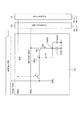
図1に実施の形態の有機EL表示装置の構成を示す。
この有機EL表示装置は、有機EL素子を発光素子とし、アクティブマトリクス方式で発光駆動を行う画素回路10を含むものである。
図示のように、有機EL表示装置は、多数の画素回路10が列方向と行方向(m行×n列)にマトリクス状に配列された画素アレイ20を有する。なお、画素回路10のそれぞれは、R(赤)、G(緑)、B(青)のいずれかの発光画素となり、各色の画素回路10が所定規則で配列されてカラー表示装置が構成される。
[1. Configuration of Display Device and Pixel Circuit]
FIG. 1 shows a configuration of an organic EL display device according to an embodiment.
This organic EL display device includes a
As illustrated, the organic EL display device includes a
各画素回路10を発光駆動するための構成として、水平セレクタ11、ドライブスキャナ12、ライトスキャナ13を備える。
また水平セレクタ11により選択され、表示データとしての輝度信号の信号値(階調値)に応じた電圧を画素回路10に供給する信号線DTL1、DTL2・・・DTL(n)が、画素アレイ上で列方向に配されている。信号線DTL1、DTL2・・・DTL(n)は、画素アレイ20においてマトリクス配置された画素回路10の列数分(n列)だけ配される。
As a configuration for driving each
Also, signal lines DTL1, DTL2,... DTL (n), which are selected by the
また画素アレイ20上において、行方向に書込制御線WSL1,WSL2・・・WSL(m)、電源制御線DSL1,DSL2・・・DSL(m)が配されている。これらの書込制御線WSL及び電源制御線DSLは、それぞれ、画素アレイ20においてマトリクス配置された画素回路10の行数分(m行)だけ配される。
On the
書込制御線WSL(WSL1〜WSL(m))はライトスキャナ13により駆動される。
ライトスキャナ13は、設定された所定のタイミングで、行状に配設された各書込制御線WSL1〜WSL(m)に順次、走査パルスWS(WS1,WS2・・・WS(m))を供給して、画素回路10を行単位で線順次走査する。
Write control lines WSL (WSL1 to WSL (m)) are driven by the
The
電源制御線DSL(DSL1〜DSL(m))はドライブスキャナ12により駆動される。ドライブスキャナ12は、ライトスキャナ13による線順次走査に合わせて、行状に配設された各電源制御線DSL1〜DSL(m)に電源パルスDS(DS1,DS2・・・DS(m))を供給する。電源パルスDS(DS1,DS2・・・DS(m))は駆動電圧Vccと初期電圧Viniの2値に切り替わるパルス電圧とされる。
なおドライブスキャナ12,ライトスキャナ13は、クロックck及びスタートパルスspに基づいて、走査パルスWS、電源パルスDSのタイミングを設定する。
The power supply control lines DSL (DSL1 to DSL (m)) are driven by the
The
水平セレクタ11は、ライトスキャナ13による線順次走査に合わせて、列方向に配された信号線DTL1、DTL2・・・に対して、画素回路10に対する入力信号としての信号線電圧を供給する。本実施の形態では、水平セレクタ11は、各信号線に対し、信号線電圧として映像データによる階調に応じた電圧である映像信号電圧Vsigを供給する。
The
なお、この実施の形態の表示装置においては、本発明請求項でいう信号セレクタの例が水平セレクタ11であり、駆動制御スキャナの例がドライブスキャナであり、書込スキャナの例がライトスキャナ13となる。
In the display device of this embodiment, an example of a signal selector referred to in the present invention is the
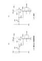
図2に実施の形態の画素回路10の構成例を示している。この画素回路10が、図1の構成における画素回路10のようにマトリクス配置される。
なお、図2では簡略化のため、信号線DTLと、書込制御線WSL(x)及び電源制御線DSL(x)が交差する部分に配される1つの画素回路10のみを示している。つまり、画素アレイ20内の第x行目における或る1つの画素回路10である。
FIG. 2 shows a configuration example of the
In FIG. 2, only one
この画素回路10は、発光素子である有機EL素子1と、保持容量Csと、第1,第2のサンプリングトランジスタTs1,Ts2、駆動トランジスタTd、基準電圧入力用トランジスタTofsを有して構成される。なお容量Coledは有機EL素子1の寄生容量である。
サンプリングトランジスタTs1、駆動トランジスタTd、及び基準電圧入力用トランジスタTofsは、nチャネルの薄膜トランジスタ(TFT)で構成され、サンプリングトランジスタTs2はpチャネルTFTで構成されている。
The
The sampling transistor Ts1, the drive transistor Td, and the reference voltage input transistor Tofs are configured by an n-channel thin film transistor (TFT), and the sampling transistor Ts2 is configured by a p-channel TFT.
保持容量Csは、一方の端子が駆動トランジスタTdのソース(ノードND2)に接続され、他方の端子が同じく駆動トランジスタTdのゲート(ノードND1)に接続されている。
画素回路10の発光素子は例えばダイオード構造の有機EL素子1とされ、アノードとカソードを備えている。有機EL素子1のアノードは駆動トランジスタTdのソースに接続され、カソードは所定の配線(カソード電位Vcat)に接続されている。
The storage capacitor Cs has one terminal connected to the source (node ND2) of the drive transistor Td and the other terminal connected to the gate (node ND1) of the drive transistor Td.
The light emitting element of the
サンプリングトランジスタTs1,Ts2は、そのソース・ドレインが信号線DTLと駆動トランジスタTdのゲート(ノードND1)の間で直列接続されている。
即ちサンプリングトランジスタTs1は、そのドレインとソースの一端が信号線DTLに接続され、他端がサンプリングトランジスタTs2に接続される。サンプリングトランジスタTs2のドレインとソースの一端はサンプリングトランジスタTs1に接続され、他端は駆動トランジスタTdのゲート(ノードND1)に接続される。
従って、サンプリングトランジスタTs1,Ts2の双方が導通したときのみ、駆動トランジスタTdのゲートに信号線DTLの信号線電圧(映像信号電圧Vsig)が入力される構成となっている。
Sampling transistors Ts1 and Ts2 have their sources and drains connected in series between the signal line DTL and the gate (node ND1) of the drive transistor Td.
That is, the sampling transistor Ts1 has one end of its drain and source connected to the signal line DTL and the other end connected to the sampling transistor Ts2. One end of the drain and source of the sampling transistor Ts2 is connected to the sampling transistor Ts1, and the other end is connected to the gate (node ND1) of the drive transistor Td.
Therefore, the signal line voltage (video signal voltage Vsig) of the signal line DTL is input to the gate of the drive transistor Td only when both of the sampling transistors Ts1 and Ts2 are turned on.
またサンプリングトランジスタTs1のゲートは、当該画素回路10の行に対応する書込制御線WSL(x)に接続されている。
一方、サンプリングトランジスタTs2のゲートは、当該画素回路10の行の前の行に対応する書込制御線WSL(x−1)に接続されている。
駆動トランジスタTdのドレインは電源制御線DSLに接続されている。
The gate of the sampling transistor Ts1 is connected to the write control line WSL (x) corresponding to the row of the
On the other hand, the gate of the sampling transistor Ts2 is connected to the write control line WSL (x−1) corresponding to the previous row of the
The drain of the drive transistor Td is connected to the power supply control line DSL.
また基準電圧入力用トランジスタTofsは、そのドレインとソースの一端が基準電圧Vofsの固定電源線に接続され、他端は駆動トランジスタTdのゲート(ノードND1)に接続されている。
基準電圧入力用トランジスタTofsのゲートは、当該画素回路10の行の前の行(第(x−1)行)に対応する書込制御線WSL(x−1)に接続されている。
基準電圧入力用トランジスタTofsがnチャネルTFTで、サンプリングトランジスタTs2がpチャネルTFTであり、ゲートが共通で書込制御線WSL(x−1)に接続されているため、基準電圧入力用トランジスタTofsとサンプリングトランジスタTs2は同時には導通しない。
The reference voltage input transistor Tofs has one end of its drain and source connected to a fixed power supply line of the reference voltage Vofs, and the other end connected to the gate (node ND1) of the drive transistor Td.
The gate of the reference voltage input transistor Tofs is connected to the write control line WSL (x−1) corresponding to the previous row ((x−1) th row) of the
Since the reference voltage input transistor Tofs is an n-channel TFT, the sampling transistor Ts2 is a p-channel TFT, and the gate is commonly connected to the write control line WSL (x−1), the reference voltage input transistor Tofs The sampling transistor Ts2 is not conductive at the same time.
有機EL素子1の発光駆動は、基本的には次のようになる。
信号線DTLに映像信号電圧Vsigが印加されたタイミングで、サンプリングトランジスタTs1,Ts2が、書込制御線WSL(x)、WSL(x−1)によってライトスキャナ13から与えられる走査パルスWS(x)、WS(x−1)によって導通される。これにより信号線DTLからの映像信号電圧Vsigが保持容量Csに書き込まれる。
The light emission driving of the
At the timing when the video signal voltage Vsig is applied to the signal line DTL, the sampling transistors Ts1, Ts2 are scanned by the write control lines WSL (x), WSL (x−1) from the
駆動トランジスタTdは、ドライブスキャナ12によって駆動電位Vccが与えられている電源制御線DSLからの電流供給により電流Idsを有機EL素子1に流し、有機EL素子1を発光させる。
このとき電流Idsは、駆動トランジスタTdのゲート・ソース間電圧Vgsに応じた値(保持容量Csに保持された電圧に応じた値)となり、有機EL素子1はその電流値に応じた輝度で発光する。
つまりこの画素回路10の場合、保持容量Csに信号線DTLからの映像信号電圧Vsigを書き込むことによって、駆動トランジスタTdのゲート印加電圧を変化させ、これにより有機EL素子1に流れる電流値をコントロールして発光の階調を得る。
The drive transistor Td causes the current Ids to flow through the
At this time, the current Ids becomes a value corresponding to the gate-source voltage Vgs of the driving transistor Td (a value corresponding to the voltage held in the holding capacitor Cs), and the
That is, in the case of this
駆動トランジスタTdは、常に飽和領域で動作するように設計されているので、駆動トランジスタTdは次の式1に示した値を持つ定電流源となる。
Ids=(1/2)・μ・(W/L)・Cox・(Vgs−Vth)2・・・(式1)
但し、Idsは飽和領域で動作するトランジスタのドレイン・ソース間に流れる電流、μは移動度、Wはチャネル幅、Lはチャネル長、Coxはゲート容量、Vthは駆動トランジスタTdの閾値電圧を表している。
この式1から明らかな様に、飽和領域ではドレイン電流Idsはゲート・ソース間電圧Vgsによって制御される。駆動トランジスタTdは、ゲート・ソース間電圧Vgsが一定に保持される為、定電流源として動作し、有機EL素子1を一定の輝度で発光させることができる。
Since the drive transistor Td is designed to always operate in the saturation region, the drive transistor Td becomes a constant current source having a value represented by the following
Ids = (1/2) · μ · (W / L) · Cox · (Vgs−Vth) 2 (Equation 1)
Where Ids is the current flowing between the drain and source of a transistor operating in the saturation region, μ is the mobility, W is the channel width, L is the channel length, Cox is the gate capacitance, and Vth is the threshold voltage of the driving transistor Td. Yes.
As apparent from
このように基本的には、各フレーム期間において、画素回路10に映像信号値(階調値)Vsigが保持容量Csに書き込まれる動作が行われ、これにより表示すべき階調に応じて駆動トランジスタTdのゲート・ソース間電圧Vgsが決まる。
そして駆動トランジスタTdは飽和領域で動作することで有機EL素子1に対して定電流源として機能し、ゲート・ソース間電圧Vgsに応じた電流を有機EL素子1に流すことで、各フレーム期間に有機EL素子1では映像信号の階調値に応じた輝度の発光が行われる。
In this way, basically, in each frame period, an operation is performed in which the video signal value (gradation value) Vsig is written in the storage capacitor Cs in the
The drive transistor Td functions as a constant current source for the
[2.本発明に至る過程で考慮された画素回路動作:分割閾値補正]
ここで、本発明の理解のため、本発明に至る過程で考慮された画素回路動作について説明する。これは、各画素回路10の駆動トランジスタTdの閾値、移動度のばらつきによるユニフォミティ劣化を補償するための閾値補正動作、移動度補正動作を含む回路動作である。特に閾値補正動作としては1発光サイクルの期間内に分割して複数回行う分割閾値補正を行う例としている。
[2. Pixel circuit operation considered in the process leading to the present invention: division threshold correction]
Here, in order to understand the present invention, the pixel circuit operation considered in the process leading to the present invention will be described. This is a circuit operation including a threshold correction operation and a mobility correction operation for compensating for uniformity deterioration due to variations in the threshold and mobility of the driving transistor Td of each
なお画素回路動作においては、閾値補正動作、移動度補正動作自体は、従来より行われているが、この必要性について簡単に説明しておく。
例えばポリシリコンTFT等を用いた画素回路では、駆動トランジスタTdの閾値電圧Vthや、駆動トランジスタTdのチャネルを構成する半導体薄膜の移動度μが経時的に変化することがある。また製造プロセスのバラツキによって閾値電圧Vthや移動度μのトランジスタ特性が画素毎に異なったりする。
駆動トランジスタTdの閾値電圧や移動度が画素毎に異なると、画素毎に駆動トランジスタTdに流れる電流値にばらつきが生じる。このため仮に全画素回路10に同一の映像信号値(映像信号電圧Vsig)を与えたとしても、有機EL素子1の発光輝度に画素毎のバラツキが生じ、その結果、画面のユニフォミティ(一様性)が損なわれる。
このことから、画素回路動作においては、閾値電圧Vthや移動度μの変動に対する補正機能を持たせるようにしている。
In the pixel circuit operation, the threshold value correction operation and the mobility correction operation itself have been performed conventionally. This necessity will be briefly described.
For example, in a pixel circuit using a polysilicon TFT or the like, the threshold voltage Vth of the drive transistor Td and the mobility μ of the semiconductor thin film constituting the channel of the drive transistor Td may change over time. Further, the transistor characteristics of the threshold voltage Vth and the mobility μ are different for each pixel due to variations in the manufacturing process.
If the threshold voltage and mobility of the drive transistor Td differ from pixel to pixel, the current value flowing through the drive transistor Td varies from pixel to pixel. For this reason, even if the same video signal value (video signal voltage Vsig) is given to all the
For this reason, the pixel circuit operation is provided with a correction function for fluctuations in the threshold voltage Vth and the mobility μ.
ここでは図3に示す一般的な画素回路10の動作として説明する。
上記図2の本実施の形態の画素回路10と比べて、第2のサンプリングトランジスタTs2と基準電圧入力用トランジスタTofsが設けられていない。
また水平セレクタ11は信号線DTLに、映像信号電圧Vsigと、閾値補正動作のための閾値補正基準電圧Vofsとを時分割で供給するものとされている。
駆動トランジスタTdからの有機EL素子1への電流印加による基本的な発光動作は同様である。
即ち信号線DTLに映像信号電圧Vsigが印加されたタイミングで、サンプリングトランジスタTsが、書込制御線WSLによってライトスキャナ13から与えられる走査パルスWSによって導通される。これにより信号線DTLからの映像信号電圧Vsigが保持容量Csに書き込まれる。
そして駆動トランジスタTdは飽和領域で動作することで有機EL素子1に対して定電流源として機能し、保持容量Csに書き込まれた映像信号電圧Vsig(ゲート・ソース間電圧Vgs)に応じた電流Idsを有機EL素子1に流す。これにより映像信号の階調値に応じた輝度の発光が行われる。
Here, the operation of the
Compared with the
The
The basic light emission operation by applying a current from the drive transistor Td to the
That is, at the timing when the video signal voltage Vsig is applied to the signal line DTL, the sampling transistor Ts is turned on by the scanning pulse WS applied from the
The drive transistor Td functions as a constant current source for the
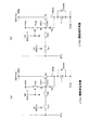
図4に画素回路10の1発光サイクル(1フレーム期間)の動作のタイミングチャートを示す。
図4では、水平セレクタ11が信号線DTLに与える信号線電圧を示している。この動作例の場合、水平セレクタ11は信号線電圧として、1水平期間(1H)に、閾値補正基準電圧Vofs及び映像信号電圧Vsigとしてのパルス電圧を信号線DTLに与える。
また図4には、電源制御線DSLを介してドライブスキャナ12から供給される電源パルスDSを示している。電源パルスDSとしては駆動電圧Vcc又は初期電圧Viniが与えられる。
また図4には、書込制御線WSLを介してライトスキャナ13によってサンプリングトランジスタTsのゲートに与えられる走査パルスWSを示している。nチャネルのサンプリングトランジスタTsは、走査パルスWSがHレベルとされることで導通され、走査パルスWSがLレベルとされることで非導通となる。
また図4には、図3に示したノードND1、ND2の電圧として、駆動トランジスタTdのゲート電圧Vgとソース電圧Vsの変化を示している。
FIG. 4 shows a timing chart of the operation of one light emission cycle (one frame period) of the
FIG. 4 shows the signal line voltage that the
FIG. 4 shows a power pulse DS supplied from the
FIG. 4 shows a scan pulse WS applied to the gate of the sampling transistor Ts by the
FIG. 4 shows changes in the gate voltage Vg and the source voltage Vs of the drive transistor Td as the voltages of the nodes ND1 and ND2 shown in FIG.
図4のタイミングチャートにおける時点tsは、発光素子である有機EL素子1が発光駆動される1サイクル、例えば画像表示の1フレーム期間の開始タイミングとなる。
この時点tsに至る前(期間LT0)は、前フレームの発光が行われている。期間LT0の等価回路を図5(a)に示す。
即ち、有機EL素子1の発光状態は、電源パルスDSが駆動電圧Vccであり、サンプリングトランジスタTsがオフした状態である。この時、駆動トランジスタTdは飽和領域で動作するように設定されているため、有機EL素子1に流れる電流Ids’は駆動トランジスタTdのゲート・ソース間電圧Vgsに応じて、上述した式1に示される値となる。
Time ts in the timing chart of FIG. 4 is a start timing of one cycle in which the
Before reaching this time point ts (period LT0), light emission of the previous frame is performed. An equivalent circuit of the period LT0 is illustrated in FIG.
That is, the light emission state of the
時点tsで今回のフレームの発光のための動作が開始される。
まず電源パルスDS=初期電位Viniとされる。図5(b)に期間LT1の等価回路を示す。
このとき、初期電位Viniが有機EL素子1の閾値電圧Vthelとカソード電圧Vcatの和よりも小さい、つまりVini ≦Vthel+Vcatであることで、有機EL素子1は消光し、非発光期間が開始される。このとき電源制御線DSLが駆動トランジスタTdのソースとなる。また有機EL素子1のアノード(ノードND2)は初期電位Viniに充電される。
The operation for light emission of the current frame is started at time ts.
First, the power supply pulse DS is set to the initial potential Vini. FIG. 5B shows an equivalent circuit of the period LT1.
At this time, when the initial potential Vini is smaller than the sum of the threshold voltage Vthel and the cathode voltage Vcat of the
一定期間後、閾値補正のための準備が行われる(期間LT2a,LT2b)。等価回路は図6(a)に示される。
即ち期間LT2a,LT2bでは、信号線DTLの電位が閾値補正基準電圧Vofsとなった時に、走査パルスWSがHレベルとされ、サンプリングトランジスタTsがオンとされる。このため駆動トランジスタTdのゲート(ノードND1)は閾値補正基準電圧Vofsとなる。
駆動トランジスタTdのゲート・ソース間電圧Vgs=Vofs−Viniとなる。
このVofs−Viniが駆動トランジスタTdの閾値電圧Vthよりも大きくないと閾値補正動作を行うことができないために、Vofs−Vini>Vthとなるように、初期電位Vini、基準電圧Vofsが設定されている。
即ち閾値補正の準備として、駆動トランジスタのゲート・ソース間電圧が、その閾値電圧Vthよりも十分広げられることになる。
After a certain period, preparation for threshold correction is performed (periods LT2a, LT2b). An equivalent circuit is shown in FIG.
That is, in the periods LT2a and LT2b, when the potential of the signal line DTL becomes the threshold correction reference voltage Vofs, the scanning pulse WS is set to the H level, and the sampling transistor Ts is turned on. Therefore, the gate (node ND1) of the drive transistor Td becomes the threshold correction reference voltage Vofs.
The gate-source voltage Vgs of the drive transistor Td is Vgs = Vofs−Vini.
Since the threshold value correction operation cannot be performed unless this Vofs−Vini is larger than the threshold voltage Vth of the drive transistor Td, the initial potential Vini and the reference voltage Vofs are set so that Vofs−Vini> Vth. .
That is, as a preparation for threshold correction, the gate-source voltage of the drive transistor is sufficiently widened than the threshold voltage Vth.
続いて閾値補正(Vth補正)が行われる。ここでは期間LT3a〜LT3dとして4回の閾値補正が行われる例としている。
まず期間LT3aとして1回目の閾値補正(Vth補正)が行われる。
この場合、信号線電圧が閾値補正基準電圧Vofsとなっているタイミングで、ライトスキャナ13が走査パルスWSをHレベルとし、またドライブスキャナ12が電源パルスDSを駆動電圧Vccとする。等価回路を図6(b)に示すが、この場合、有機EL素子1のアノード(ノードND2)が駆動トランジスタTdのソースとなり電流が流れる。このため、駆動トランジスタTdのゲート(ノードND1)は閾値補正基準電圧Vofsに固定されたまま、ソースノードが上昇する。
有機EL素子1のアノード電位(ノードND2の電位)が、Vcat+Vthel(有機EL素子1の閾値電圧)以下である限り、駆動トランジスタTdの電流は保持容量Csと容量Coledを充電するために使われる。有機EL素子1のアノード電位がVcat+Vthel以下である限りとは、有機EL素子1のリーク電流が駆動トランジスタTdに流れる電流よりもかなり小さいという意味である。
このためノードND2の電位(駆動トランジスタTdのソース電位)は、時間と共に上昇してゆく。
Subsequently, threshold correction (Vth correction) is performed. Here, an example is shown in which threshold correction is performed four times during the periods LT3a to LT3d.
First, during the period LT3a, the first threshold correction (Vth correction) is performed.
In this case, at the timing when the signal line voltage becomes the threshold correction reference voltage Vofs, the
As long as the anode potential of the organic EL element 1 (potential of the node ND2) is equal to or lower than Vcat + Vthel (threshold voltage of the organic EL element 1), the current of the drive transistor Td is used to charge the storage capacitor Cs and the capacitor Coled. “As long as the anode potential of the
For this reason, the potential of the node ND2 (the source potential of the driving transistor Td) increases with time.
この閾値補正は、基本的には、駆動トランジスタTdのゲート・ソース間電圧を閾値電圧Vthとする動作と言える。従って駆動トランジスタTdのゲート・ソース間電圧が閾値電圧Vthとなるまで、駆動トランジスタTdのソース電位が上昇されればよい。
しかし、ゲートノードを閾値補正基準電圧Vofsに固定できるのは、信号線電圧=Vofsの期間のみである。するとフレームレート等によっては1回の閾値補正動作によっては、ゲート・ソース間電圧が閾値電圧Vthに至るまでソース電位が上昇するための十分な時間がとれない。そこで複数回に分割して閾値補正を行うようにしている。
This threshold correction is basically an operation of setting the gate-source voltage of the drive transistor Td to the threshold voltage Vth. Therefore, the source potential of the drive transistor Td only needs to be raised until the gate-source voltage of the drive transistor Td reaches the threshold voltage Vth.
However, the gate node can be fixed to the threshold correction reference voltage Vofs only during the period of the signal line voltage = Vofs. Then, depending on the frame rate or the like, sufficient time for the source potential to rise cannot be taken by the threshold correction operation once until the gate-source voltage reaches the threshold voltage Vth. Therefore, the threshold value correction is performed in a plurality of times.
このため、信号線電圧=映像信号電圧Vsigとなる前に、期間LT3aとしての閾値補正を終了させる。即ち、ライトスキャナ13が一旦、走査パルスWSをLレベルとし、サンプリングトランジスタTsをオフする。
このとき、ゲート・ソースともフローティングである為、ゲート・ソース間電圧Vgsに応じてドレイン・ソース間に電流が流れブートストラップする。即ち図示のようにゲート電位、ソース電位は上昇する。
For this reason, the threshold correction as the period LT3a is ended before the signal line voltage = the video signal voltage Vsig. That is, the
At this time, since both the gate and the source are floating, a current flows between the drain and the source in accordance with the gate-source voltage Vgs and bootstraps. That is, the gate potential and the source potential rise as shown.
次に期間LT3bとして、2回目の閾値補正を行う。即ち信号線電圧=閾値補正基準電圧Vofsのときに、再びライトスキャナ13が走査パルスWSをHレベルとし、サンプリングトランジスタTsをオンとする。これにより、駆動トランジスタTdのゲート電圧=閾値補正基準電圧Vofsとされ、またソース電位が上昇される。
さらに閾値補正動作を休止する。なお、2回目の閾値補正で駆動トランジスタTdのゲート・ソース間電圧は、より閾値電圧Vthに近づいているため、2回目の休止期間のブートストラップ量は1回目の休止期間より小さくなる。
また期間LT3cで3回目の閾値補正を行い、さらに休止を経て、期間LT3dで4回目の閾値補正を行う。
そして最終的に駆動トランジスタTdのゲート・ソース間電圧が閾値電圧Vthとなる。
この時、ソース電位(ノードND2:有機EL素子1のアノード電位)=Vofs−Vth≦Vcat+Vthelとなっている。(Vcatはカソード電位、Vthelは有機EL素子1の閾値電圧)
この図4の場合では、4回目の閾値補正の期間LT3dの後、走査パルスWSをLレベルとし、サンプリングトランジスタTsがオフとなって閾値補正動作が完了する。
Next, in the period LT3b, the second threshold correction is performed. That is, when signal line voltage = threshold correction reference voltage Vofs, the
Further, the threshold correction operation is paused. Since the gate-source voltage of the drive transistor Td is closer to the threshold voltage Vth in the second threshold correction, the bootstrap amount in the second pause period is smaller than that in the first pause period.
Further, the third threshold correction is performed in the period LT3c, and after a pause, the fourth threshold correction is performed in the period LT3d.
Finally, the gate-source voltage of the drive transistor Td becomes the threshold voltage Vth.
At this time, the source potential (node ND2: anode potential of the organic EL element 1) = Vofs−Vth ≦ Vcat + Vthel. (Vcat is the cathode potential, Vthel is the threshold voltage of the organic EL element 1)
In the case of FIG. 4, after the fourth threshold correction period LT3d, the scanning pulse WS is set to L level, the sampling transistor Ts is turned off, and the threshold correction operation is completed.
なお、ここでは4回の閾値補正を行う例としたが、閾値補正動作を何回に分割して行うかは表示装置の構成や動作に応じて適切に決められるものであり、例えば2回、3回、5回以上という例もある。 In this example, the threshold correction is performed four times. However, how many times the threshold correction operation is performed can be appropriately determined according to the configuration and operation of the display device. There are also examples of 3 times, 5 times or more.
その後、信号線電圧が映像信号電圧Vsigとなっている期間LT4に、ライトスキャナ13が走査パルスWSがHレベルとし、映像信号電圧Vsigの書込及び移動度補正が行われる。即ち駆動トランジスタTdのゲートに映像信号電圧Vsigが入力される。このときの等価回路を図7(a)に示す。
Thereafter, during a period LT4 in which the signal line voltage is the video signal voltage Vsig, the
駆動トランジスタTdのゲート電位は映像信号電圧Vsigの電位となるが、電源制御線DSLが駆動電圧Vccとなっていることで電流が流れ、ソース電位は時間とともに上昇してゆく。
このとき、駆動トランジスタTdのソース電圧が有機EL素子1の閾値電圧Vthelとカソード電圧Vcatの和を越えなければ、駆動トランジスタTdの電流は保持容量Csと容量Coledを充電するのに使用される。つまり有機EL素子1のリーク電流が駆動トランジスタTdに流れる電流よりもかなり小さければという条件である。
そしてこのときは、駆動トランジスタTdの閾値補正動作は完了しているため、駆動トランジスタTdが流す電流は移動度μを反映したものとなる。
具体的にいうと、移動度が大きいものはこの時の電流量が大きく、ソースの上昇も早い。逆に移動度が小さいものは電流量が小さく、ソースの上昇は遅くなる。
これによって、走査パルスWSがHレベルとなる期間LT4として、サンプリングトランジスタTsがオンしてから、駆動トランジスタTdのソース電圧Vsは上昇し、サンプリングトランジスタTsがオフしたときには、ソース電圧Vsは移動度μを反映した電圧Vs0となる。駆動トランジスタTdのゲート・ソース間電圧Vgsは移動度を反映して小さくなり(Vgs=Vsig−Vs0)、一定時間経過後に完全に移動度を補正する電圧となる。
The gate potential of the drive transistor Td becomes the potential of the video signal voltage Vsig, but current flows because the power supply control line DSL is at the drive voltage Vcc, and the source potential rises with time.
At this time, if the source voltage of the driving transistor Td does not exceed the sum of the threshold voltage Vthel and the cathode voltage Vcat of the
At this time, since the threshold value correcting operation of the drive transistor Td is completed, the current flowing through the drive transistor Td reflects the mobility μ.
Specifically, those with high mobility have a large current amount at this time, and the source rises quickly. On the other hand, when the mobility is low, the amount of current is small and the source rises slowly.
As a result, during the period LT4 when the scanning pulse WS is at the H level, the source voltage Vs of the drive transistor Td rises after the sampling transistor Ts is turned on, and when the sampling transistor Ts is turned off, the source voltage Vs becomes the mobility μ The voltage Vs0 reflects the above. The gate-source voltage Vgs of the drive transistor Td is reduced to reflect the mobility (Vgs = Vsig−Vs0), and becomes a voltage that completely corrects the mobility after a predetermined time has elapsed.
このように映像信号電圧Vsig書込及び移動度補正を行った後、ゲート・ソース間電圧Vgsを確定させ、ブートストラップ、発光状態(期間LT5)へと移行する。図7(b)に等価回路を示す。
即ち走査パルスWSをLレベルとしてサンプリングトランジスタTsをオフして書き込みが終了し、有機EL素子1を発光させる。この場合、駆動トランジスタTdのゲート・ソース間電圧Vgsに応じた電流Idsが流れ、ノードND2の電位は、有機EL素子1にその電流が流れる電圧VELまで上昇し、有機EL素子1は発光する。このときサンプリングトランジスタTsがオフであり、ノードND2の電位の上昇と同時に駆動トランジスタTdのゲート(ノードND1)も同様に上昇するため、ゲート・ソース間電圧Vgsは一定に保たれたままである。(ブートストラップ動作)
After writing the video signal voltage Vsig and correcting the mobility in this way, the gate-source voltage Vgs is determined, and the process proceeds to the bootstrap and light emission state (period LT5). FIG. 7B shows an equivalent circuit.
That is, the scanning pulse WS is set to L level, the sampling transistor Ts is turned off, writing is completed, and the
このように画素回路10は1フレーム期間における1サイクルの発光駆動動作として、閾値補正動作及び移動度補正動作を含んで、有機EL素子1の発光のための動作が行われる。
閾値補正動作によって、各画素回路10での駆動トランジスタTdの閾値電圧Vthのバラツキや、経時変動による閾値電圧Vth変動などに関わらず、信号電位Vsigに応じた電流を有機EL素子1に与えることができる。つまり製造上或いは経時変化による閾値電圧Vthのバラツキをキャンセルして、画面上に輝度ムラ等を発生させずに高画質を維持できる。
また、駆動トランジスタTdの移動度によってもドレイン電流は変動するため、画素回路10毎の駆動トランジスタTdの移動度のバラツキにより画質が低下するが、移動度補正により、駆動トランジスタTdの移動度の大小に応じてソース電位Vsが得られる。結果として各画素回路10の駆動トランジスタTdの移動度のバラツキを吸収するようなゲート・ソース間電圧Vgsに調整されるため、移動度のバラツキによる画質低下も解消される。
As described above, the
By the threshold correction operation, a current corresponding to the signal potential Vsig can be supplied to the
In addition, since the drain current varies depending on the mobility of the driving transistor Td, the image quality deteriorates due to variations in the mobility of the driving transistor Td for each
また1サイクルの画素回路動作として、閾値補正動作を分割して複数回行うのは、表示装置の高速化(高周波数化)の要請による。
高フレームレート化が進むことで、画素回路の動作時間が相対的に短くなっていくため、連続的な閾値補正期間(信号線電圧=閾値補正基準電圧Vofsの期間)を確保することが難しくなる。そこで上記のように時分割的に閾値補正動作を行うことで閾値補正期間として必要な期間を確保して、駆動トランジスタTdのゲート・ソース間電圧を閾値電圧Vthに収束させるものである。
Further, the threshold correction operation is divided and performed a plurality of times as the pixel circuit operation in one cycle because of a demand for high speed display (high frequency).
As the frame rate is increased, the operation time of the pixel circuit is relatively shortened, so that it is difficult to secure a continuous threshold correction period (signal line voltage = threshold correction reference voltage Vofs period). . Thus, by performing the threshold correction operation in a time-sharing manner as described above, a necessary period is secured as the threshold correction period, and the gate-source voltage of the drive transistor Td is converged to the threshold voltage Vth.
ところが、駆動の高速化に伴い、次の点で不利となった。
図4の信号線電圧からわかるように、水平セレクタ11は1水平期間に映像信号電圧Vsigと閾値補正基準電圧Vofsを信号線DTLに時分割出力している。
ハイフレームレート化などにより駆動高速化が進むと1水平期間も短くなるが、すると水平セレクタ11の時分割出力の動作マージンが低下する。また処理負担の増大や水平セレクタ11内の信号線DTLに対するドライバの高性能化の要請も生じ、コスト増にもつながる。
However, as the drive speeded up, the following points were disadvantageous.
As can be seen from the signal line voltage in FIG. 4, the
As the driving speed increases due to the high frame rate or the like, one horizontal period is also shortened. However, the operation margin of the time division output of the
[3.実施の形態の画素回路動作]
そこで本実施の形態では、水平セレクタ11が時分割出力を必要とせず、映像信号電圧Vsigのみを出力すればよいようにすることを提案する。もちろん、それによって画質劣化等が生ずることは避けなければならない。そこで、信号線DTL以外で画素回路に閾値補正基準電圧Vofsを導入して閾値補正を実行できる構成を採る。さらに、それによっても新たな制御線などによるパネル構成の複雑化が生じないようにもする。
[3. Pixel Circuit Operation of Embodiment]
Therefore, in this embodiment, it is proposed that the
これらの目的のため、本実施の形態では画素回路10は上述した図2の構成を採る。そして、図8のような駆動タイミングで画素回路10を動作させる。
図8で説明する動作は、画素回路10が、その画素回路10の行の書込制御線WSL(x)の走査パルスWS(x)と、その画素回路10の前の行の書込制御線WSL(x−1)の走査パルスWS(x−1)によって、駆動トランジスタTdのゲート・ソース間電圧Vgsを、駆動トランジスタTdの閾値電圧Vthとする閾値補正動作である。さらに、走査パルスWS(x)、WS(x−1)によって、駆動トランジスタTdのゲート・ソース間への信号線DTLからの映像信号電圧Vsigの入力動作が制御される動作である。
For these purposes, in the present embodiment, the
In the operation described in FIG. 8, the
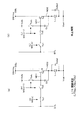
図8では画素回路10の1発光サイクル(1フレーム期間)の動作のタイミングチャートを示している。
図8では、水平セレクタ11が信号線DTLに与える信号線電圧を示している。この動作例の場合、水平セレクタ11は信号線電圧として、1水平期間(1H)毎に1つの画素回路10に対する映像信号電圧Vsigを信号線DTLに与える。
つまり水平セレクタ11は閾値補正基準電圧Vofsの出力は行わない。図2に示したように、閾値補正基準電圧Vofsは、固定電源線から基準電圧入力用トランジスタTofsを介して画素回路10内に導入される。
また図8には、電源制御線DSLを介してドライブスキャナ12から供給される電源パルスDSを示している。電源パルスDSとしては駆動電圧Vcc又は初期電圧Viniが与えられる。
FIG. 8 shows a timing chart of the operation of one light emission cycle (one frame period) of the
FIG. 8 shows the signal line voltage applied to the signal line DTL by the
That is, the
FIG. 8 shows a power pulse DS supplied from the
また図8には、書込制御線WSLを介してライトスキャナ13によってサンプリングトランジスタTsのゲートに与えられる走査パルスWSを示している。ここでは、当該画素回路10の行に対応する書込制御線WSL(x)からの走査パルスWS(x)と、その前の行に対応する書込制御線WSL(x−1)からの走査パルスWS(x−1)を示している。
各行の走査パルスWSは、例えばライトスキャナ13内のシフトレジスタを介して図1に示した各書込制御線WSL1〜WSL(m)に出力される。このため、走査パルスWS(x)は、走査パルスWS(x−1)に対して1水平期間遅れた波形となる。
nチャネルのサンプリングトランジスタTs1は、走査パルスWS(x)がHレベルとされることで導通され、走査パルスWS(x)がLレベルとされることで非導通となる。
pチャネルのサンプリングトランジスタTs2は、走査パルスWS(x−1)がLレベルとされることで導通され、走査パルスWS(x−1)がHレベルとされることで非導通となる。
nチャネルの基準電圧入力用トランジスタTofsは、走査パルスWS(x−1)がHレベルとされることで導通され、走査パルスWS(x−1)がLレベルとされることで非導通となる。
FIG. 8 shows a scanning pulse WS applied to the gate of the sampling transistor Ts by the
The scanning pulse WS of each row is output to each of the write control lines WSL1 to WSL (m) shown in FIG. 1 via, for example, a shift register in the
The n-channel sampling transistor Ts1 is turned on when the scanning pulse WS (x) is set to the H level, and is turned off when the scanning pulse WS (x) is set to the L level.
The p-channel sampling transistor Ts2 is turned on when the scan pulse WS (x-1) is set to the L level, and is turned off when the scan pulse WS (x-1) is set to the H level.
The n-channel reference voltage input transistor Tofs is turned on when the scan pulse WS (x-1) is set to H level, and is turned off when the scan pulse WS (x-1) is set to L level. .
また図8には、ノードND1、ND2の電圧として、駆動トランジスタTdのゲート電圧Vgとソース電圧Vsの変化を示している。 FIG. 8 shows changes in the gate voltage Vg and the source voltage Vs of the drive transistor Td as the voltages of the nodes ND1 and ND2.
図8の動作を説明する。図8のタイミングチャートにおける時点tsは、発光素子である有機EL素子1が発光駆動される1サイクル、例えば画像表示の1フレーム期間の開始タイミングとなる。
この時点tsに至る前(期間LT0)は、前フレームの発光が行われている。期間LT0の等価回路を図9(a)に示す。
即ち、有機EL素子1の発光状態は、電源パルスDSが駆動電圧Vccであり、サンプリングトランジスタTsがオフした状態である。サンプリングトランジスタTs2はオンであるが、サンプリングトランジスタTs1のオフにより、ノードND1は信号線DTLから切り離されている。また、基準電圧入力用トランジスタTofsもオフであり、ノードND1は基準電圧Vofsの固定電源線からも切り離されている。
この時、駆動トランジスタTdは飽和領域で動作するように設定されているため、有機EL素子1に流れる電流Ids’は駆動トランジスタTdのゲート・ソース間電圧Vgsに応じて、上述した式1に示される値となる。
The operation of FIG. 8 will be described. A time point ts in the timing chart of FIG. 8 is a start timing of one cycle in which the
Before reaching this time point ts (period LT0), light emission of the previous frame is performed. FIG. 9A shows an equivalent circuit of the period LT0.
That is, the light emission state of the
At this time, since the drive transistor Td is set to operate in the saturation region, the current Ids ′ flowing through the
時点tsで今回のフレームの発光のための動作が開始される。
まず電源パルスDS=初期電位Viniとされる。このとき、初期電位Viniが有機EL素子1の閾値電圧Vthelとカソード電圧Vcatの和よりも小さい、つまりVini ≦Vthel+Vcatであることで、有機EL素子1は消光し、非発光期間が開始される。図9(b)に示すように、このとき電源制御線DSLが駆動トランジスタTdのソースとなり、有機EL素子1のアノード(ノードND2)は初期電位Viniに充電される。
The operation for light emission of the current frame is started at time ts.
First, the power supply pulse DS is set to the initial potential Vini. At this time, when the initial potential Vini is smaller than the sum of the threshold voltage Vthel and the cathode voltage Vcat of the
一定期間後、閾値補正のための準備が行われる(期間LT2a,LT2b)。
まず、期間LT2aでは、走査パルスWS(x−1)がHレベルとなる。等価回路を図10(a)に示すように基準電圧入力用トランジスタTofsがオンとなる。サンプリングトランジスタTs1,Ts2は共にオフである。
このため駆動トランジスタTdのゲート(ノードND1)には、固定電源線からの閾値補正基準電圧Vofsが入力される。従って駆動トランジスタTdのゲート・ソース間電圧Vgsは、Vofs−Viniとなる。
After a certain period, preparation for threshold correction is performed (periods LT2a, LT2b).
First, in the period LT2a, the scanning pulse WS (x-1) is at the H level. In the equivalent circuit shown in FIG. 10A, the reference voltage input transistor Tofs is turned on. The sampling transistors Ts1 and Ts2 are both off.
Therefore, the threshold correction reference voltage Vofs from the fixed power supply line is input to the gate (node ND1) of the drive transistor Td. Therefore, the gate-source voltage Vgs of the driving transistor Td is Vofs−Vini.
また、期間LT2bでは、走査パルスWS(x−1)がHレベルとなる。等価回路を図10(b)に示すように基準電圧入力用トランジスタTofsがオン、サンプリングトランジスタTs1がオン、サンプリングトランジスタTs2がオフの状態となる。
このときも、駆動トランジスタTdのゲート(ノードND1)には、固定電源線からの閾値補正基準電圧Vofsが入力される。従って駆動トランジスタTdのゲート・ソース間電圧VgsはVofs−Viniである。
この期間LT2a,LT2bでは、この閾値補正の準備として、駆動トランジスタのゲート・ソース間電圧Vgsを、その閾値電圧Vthよりも十分広げらるものである。ゲート・ソース間電圧Vgs(この場合Vgs=Vofs−Vini)が駆動トランジスタTdの閾値電圧Vthよりも大きくないと閾値補正動作を行うことができないため、Vofs−Vini>Vthとなるように、初期電位Vini、基準電圧Vofsが設定されている。
Further, in the period LT2b, the scanning pulse WS (x-1) is at the H level. As shown in FIG. 10B, the equivalent circuit is such that the reference voltage input transistor Tofs is on, the sampling transistor Ts1 is on, and the sampling transistor Ts2 is off.
Also at this time, the threshold correction reference voltage Vofs from the fixed power supply line is input to the gate (node ND1) of the drive transistor Td. Therefore, the gate-source voltage Vgs of the drive transistor Td is Vofs−Vini.
In this period LT2a, LT2b, as a preparation for the threshold correction, the gate-source voltage Vgs of the driving transistor is sufficiently widened than the threshold voltage Vth. Since the threshold value correcting operation cannot be performed unless the gate-source voltage Vgs (in this case, Vgs = Vofs−Vini) is larger than the threshold voltage Vth of the driving transistor Td, the initial potential is set so that Vofs−Vini> Vth. Vini and reference voltage Vofs are set.
続いて閾値補正(Vth補正)を行う。ここでは期間LT3a〜LT3cとして3回の閾値補正が行われる例としている。
まず期間LT3aとして1回目の閾値補正(Vth補正)が行われる。
この場合、ライトスキャナ13が走査パルスWS(x)、WS(x−1)をHレベルとする期間において、ドライブスキャナ12が電源パルスDSを駆動電圧Vccとする。等価回路を図11(a)に示すが、この場合、有機EL素子1のアノード(ノードND2)が駆動トランジスタTdのソースとなり電流が流れる。このため、駆動トランジスタTdのゲート(ノードND1)は閾値補正基準電圧Vofsに固定されたまま、ソースノードが上昇する。
有機EL素子1のアノード電位(ノードND2の電位)が、Vcat+Vthel(有機EL素子1の閾値電圧)以下である限り、駆動トランジスタTdの電流は保持容量Csと容量Coledを充電するために使われる。有機EL素子1のアノード電位がVcat+Vthel以下である限りとは、有機EL素子1のリーク電流が駆動トランジスタTdに流れる電流よりもかなり小さいという意味である。
このためノードND2の電位(駆動トランジスタTdのソース電位)は、図8に示すように時間と共に上昇してゆく。
Subsequently, threshold correction (Vth correction) is performed. Here, an example is shown in which threshold correction is performed three times during the periods LT3a to LT3c.
First, during the period LT3a, the first threshold correction (Vth correction) is performed.
In this case, the
As long as the anode potential of the organic EL element 1 (potential of the node ND2) is equal to or lower than Vcat + Vthel (threshold voltage of the organic EL element 1), the current of the drive transistor Td is used to charge the storage capacitor Cs and the capacitor Coled. “As long as the anode potential of the
Therefore, the potential of the node ND2 (the source potential of the driving transistor Td) increases with time as shown in FIG.
期間LT3aとしての1回目の閾値補正動作は、走査パルスWS(x)、WS(x−1)がLレベルとなることで終了し、休止期間に入る。休止期間の等価回路は図11(b)のようになる。即ちサンプリングトランジスタTs1と基準電圧入力用トランジスタTofsがオフ、サンプリングトランジスタTs2はオンとなる。
このとき、駆動トランジスタTdのゲート、ソースともフローティングである為、ゲート・ソース間電圧Vgsに応じてドレイン・ソース間に電流が流れブートストラップする。即ち図8のようにゲート電位Vg、ソース電位Vsは上昇する。
The first threshold correction operation as the period LT3a ends when the scanning pulses WS (x) and WS (x-1) become L level, and enters a pause period. An equivalent circuit in the idle period is as shown in FIG. That is, the sampling transistor Ts1 and the reference voltage input transistor Tofs are turned off, and the sampling transistor Ts2 is turned on.
At this time, since the gate and the source of the driving transistor Td are both floating, a current flows between the drain and the source in accordance with the gate-source voltage Vgs and bootstraps. That is, as shown in FIG. 8, the gate potential Vg and the source potential Vs rise.
次に期間LT3bとして、走査パルスWS(x)、WS(x−1)がHレベルとなることで、2回目の閾値補正が行われる。等価回路でいえば再び図11(a)の状態となる。
これにより、駆動トランジスタTdのゲート電圧=閾値補正基準電圧Vofsとされ、またソース電位が上昇される。
さらに走査パルスWS(x)、WS(x−1)がLレベルとなることで閾値補正動作が休止される。なお、2回目の閾値補正で駆動トランジスタTdのゲート・ソース間電圧は、より閾値電圧Vthに近づいているため、2回目の休止期間のブートストラップ量は1回目の休止期間より小さくなる。
また期間LT3cで、走査パルスWS(x)、WS(x−1)がHレベルとなることで3回目の閾値補正を行う。
そして最終的に駆動トランジスタTdのゲート・ソース間電圧が閾値電圧Vthとなる。
この時、ソース電位(ノードND2:有機EL素子1のアノード電位)=Vofs−Vth≦Vcat+Vthelとなっている。(Vcatはカソード電位、Vthelは有機EL素子1の閾値電圧)
この図8の場合では、3回目の閾値補正の期間LT3cの終了後、閾値補正動作が完了する。
Next, as the period LT3b, the scan pulse WS (x), WS (x-1) is set to the H level, and the second threshold correction is performed. Speaking of an equivalent circuit, the state shown in FIG.
As a result, the gate voltage of the drive transistor Td = the threshold correction reference voltage Vofs, and the source potential is increased.
Further, the threshold correction operation is stopped when the scanning pulses WS (x) and WS (x−1) become L level. Since the gate-source voltage of the drive transistor Td is closer to the threshold voltage Vth in the second threshold correction, the bootstrap amount in the second pause period is smaller than that in the first pause period.
In the period LT3c, the third threshold correction is performed when the scanning pulses WS (x) and WS (x-1) are at the H level.
Finally, the gate-source voltage of the drive transistor Td becomes the threshold voltage Vth.
At this time, the source potential (node ND2: anode potential of the organic EL element 1) = Vofs−Vth ≦ Vcat + Vthel. (Vcat is the cathode potential, Vthel is the threshold voltage of the organic EL element 1)
In the case of FIG. 8, the threshold correction operation is completed after the end of the third threshold correction period LT3c.
その後、信号線電圧が、当該画素回路10に対する映像信号電圧Vsig(x)となっている期間LT4に、映像信号電圧Vsigの書込及び移動度補正が行われる。
上述のように走査パルスWS(x)とWS(x−1)は1水平期間ずれたパルスであり、この期間LT4では、走査パルスWS(x)はHレベル、走査パルスWS(x−1)はLレベルとなっている。
従って図12(a)に示すように、サンプリングトランジスタTs1,Ts2の双方がオンとなり、基準電圧入力用トランジスタTofsはオフとなる。
このため駆動トランジスタTdのゲートに信号線DTLからの映像信号電圧Vsig(x)の書込が行われる。
Thereafter, the writing of the video signal voltage Vsig and the mobility correction are performed during a period LT4 in which the signal line voltage is the video signal voltage Vsig (x) for the
As described above, the scan pulses WS (x) and WS (x-1) are pulses shifted by one horizontal period. In this period LT4, the scan pulse WS (x) is at the H level and the scan pulse WS (x-1). Is at L level.
Accordingly, as shown in FIG. 12A, both the sampling transistors Ts1 and Ts2 are turned on, and the reference voltage input transistor Tofs is turned off.
Therefore, the video signal voltage Vsig (x) from the signal line DTL is written to the gate of the drive transistor Td.
駆動トランジスタTdのゲート電位は映像信号電圧Vsigの電位となるが、電源制御線DSLが駆動電圧Vccとなっていることで電流が流れ、ソース電位は時間とともに上昇していく。
このとき、駆動トランジスタTdのソース電圧が有機EL素子1の閾値電圧Vthelとカソード電圧Vcatの和を越えなければ、駆動トランジスタTdの電流は保持容量Csと容量Coledを充電するのに使用される。そして駆動トランジスタTdが流す電流は移動度μを反映したものとなる。
即ち、移動度が大きいものはこの時の電流量が大きく、ソースの上昇も早い。逆に移動度が小さいものは電流量が小さく、ソースの上昇は遅くなる。これによって、走査パルスWSがHレベルとなる期間LT4として、サンプリングトランジスタTsがオンしてから、駆動トランジスタTdのソース電圧Vsは上昇し、サンプリングトランジスタTsがオフしたときには、ソース電圧Vsは移動度μを反映した電圧Vs0となる。駆動トランジスタTdのゲート・ソース間電圧Vgsは移動度μを反映して小さくなり(Vgs=Vsig−Vs0)、一定時間経過後に完全に移動度μを補正する電圧となる。
The gate potential of the drive transistor Td becomes the potential of the video signal voltage Vsig. However, since the power supply control line DSL is at the drive voltage Vcc, a current flows and the source potential increases with time.
At this time, if the source voltage of the driving transistor Td does not exceed the sum of the threshold voltage Vthel and the cathode voltage Vcat of the
That is, when the mobility is high, the amount of current at this time is large and the source rises quickly. On the other hand, when the mobility is low, the amount of current is small and the source rises slowly. As a result, during the period LT4 when the scanning pulse WS is at the H level, the source voltage Vs of the drive transistor Td rises after the sampling transistor Ts is turned on, and when the sampling transistor Ts is turned off, the source voltage Vs becomes the mobility μ The voltage Vs0 reflects the above. The gate-source voltage Vgs of the driving transistor Td is reduced to reflect the mobility μ (Vgs = Vsig−Vs0), and becomes a voltage that completely corrects the mobility μ after a predetermined time has elapsed.
このように映像信号電圧Vsig書込及び移動度補正を行った後、ゲート・ソース間電圧Vgsを確定させ、ブートストラップ、発光状態(期間LT5)へと移行する。
即ち走査パルスWSをLレベルとしてサンプリングトランジスタTs1をオフして書き込みが終了し、有機EL素子1を発光させる。等価回路は図12(b)のようになる。
この場合、駆動トランジスタTdのゲート・ソース間電圧Vgsに応じた電流Idsが流れ、ノードND2の電位は、有機EL素子1にその電流が流れる電圧VELまで上昇し、有機EL素子1は発光する。このときサンプリングトランジスタTs1及び基準電圧入力用トランジスタTofsがオフであり、ノードND2の電位の上昇と同時に駆動トランジスタTdのゲート(ノードND1)も同様に上昇するため、ゲート・ソース間電圧Vgsは一定に保たれたままである。(ブートストラップ動作)
After writing the video signal voltage Vsig and correcting the mobility in this way, the gate-source voltage Vgs is determined, and the process proceeds to the bootstrap and light emission state (period LT5).
That is, the scanning pulse WS is set to L level, the sampling transistor Ts1 is turned off, writing is completed, and the
In this case, a current Ids corresponding to the gate-source voltage Vgs of the drive transistor Td flows, the potential of the node ND2 rises to the voltage VEL through which the current flows in the
このように画素回路10は1フレーム期間における1サイクルの発光駆動動作として、閾値補正動作及び移動度補正動作を含んで、有機EL素子1の発光のための動作が行われる。
As described above, the
以上のように本実施の形態の場合、各画素回路10のサンプリングトランジスタTs1は、その画素回路10の行の書込制御線WSL(x)の走査パルスWS(x)によって導通制御される。またサンプリングトランジスタTs2と、基準電圧入力用トランジスタTofsは、その画素回路10の前の行の書込制御線WSL(x−1)の走査パルスWS(x−1)によって導通制御される。
そして、各画素回路10では、ドライブスキャナ12が駆動トランジスタTdに駆動電圧Vccを与えるときに、前の行の走査パルスWS(x−1)によって、サンプリングトランジスタTs2がオフ、基準電圧入力用トランジスタTofsがオンとされることで、閾値補正動作が行われる(期間LT3)。この閾値補正動作は、1発光サイクルの期間内に複数回(期間LT3a,LT3b,LT3c)行われる。
また各画素回路10では、水平セレクタ11が、その画素回路10に対する映像信号電圧Vsig(x)を信号線DTLに与えるときに、その画素回路の行及び前の行についての走査パルスWS(x)、WS(x−1)によって、サンプリングトランジスタTs1,Ts2がオンとされ、基準電圧入力用トランジスタがオフとされることで、映像信号電圧Vsig(x)の入力動作が行われる。
As described above, in the case of the present embodiment, the conduction of the sampling transistor Ts1 of each
In each
In each
このことから、水平セレクタ11は信号線DTLに対して映像信号電圧Vsigの供給を行えば良く、閾値補正基準電圧Vofsを供給する必要はない。つまり図4の場合のような時分割供給は不要である。これにより、画素駆動の高速化が進み、1水平期間が短くなっても、水平セレクタ11の処理負担は過大とならず、高速処理化に有利であり、動作マージンを拡大できる。また水平セレクタ11についてコスト的にも有利である。
その上で、閾値補正基準電圧Vofsを用いた閾値補正は実行されるため、駆動高速化と画質向上が両立できる。
さらに閾値補正基準電圧Vofsの画素回路10への供給のための制御は、前の行の走査パルスWS(x−1)を用いることで、新たな独立した制御線構成は不要である。従って画素アレイ20の構成の複雑化等も招かない。
Therefore, the
In addition, since threshold correction using the threshold correction reference voltage Vofs is executed, both driving speed improvement and image quality improvement can be achieved.
Furthermore, the control for supplying the threshold correction reference voltage Vofs to the
以上、実施の形態について説明したが、本発明は上記例に限定されるものではない。
上記例では1発光サイクル内に3回の閾値補正を行う例としたが、閾値補正動作を何回に分割して行うかは表示装置の構成や動作に応じて適切に決められるものであり、例えば2回或いは4回以上という例もある。さらに、必ずしも複数回の閾値補正動作を行う方式に限定されない。1回の閾値補正動作で閾値補正が完了するのであれば、1回でもよい。
また、画素回路10の構成は図2に限定されない。例えばサンプリングトランジスタTs1,Ts2及び基準電圧入力用トランジスタTofsのnチャネル、pチャネルは逆でもよい。もちろんその場合は走査パルスWSの制御論理は逆となる。
さらに、前の行の走査パルスWS(x−1)の制御によって、固定電源線から閾値補正基準電圧VofsをノードND1に導入できる回路構成であれば、他の構成でもよい。
Although the embodiment has been described above, the present invention is not limited to the above example.
In the above example, the threshold correction is performed three times within one light emission cycle. However, how many times the threshold correction operation is performed can be appropriately determined according to the configuration and operation of the display device. For example, there are examples of two times or four times or more. Furthermore, the method is not necessarily limited to a method of performing a threshold correction operation a plurality of times. If threshold correction is completed by one threshold correction operation, it may be performed once.
Further, the configuration of the
Furthermore, any other configuration may be used as long as the threshold correction reference voltage Vofs can be introduced from the fixed power supply line to the node ND1 by controlling the scan pulse WS (x−1) in the previous row.
1 有機EL素子、10 画素回路、11 水平セレクタ、12 ドライブスキャナ、13 ライトスキャナ、20 画素アレイ部、Cs 保持容量、Ts1,Ts2 サンプリングトランジスタ、Td 駆動トランジスタ、Tofs 基準電圧入力用トランジスタTofs
DESCRIPTION OF
Claims (6)
上記画素アレイ上で列状に配設される各信号線に映像信号電圧を供給する信号セレクタと、
上記画素アレイ上で行状に配設される各電源制御線に電源パルスを与え、上記画素回路の上記駆動トランジスタへの駆動電圧の印加を行う駆動制御スキャナと、
上記画素アレイ上で行状に配設される各書込制御線に走査パルスを与えて上記画素回路への上記映像信号電圧の入力を実行させる書込スキャナと、
を備え、
上記画素アレイにおける各画素回路は、その画素回路の行の書込制御線の走査パルスと、その画素回路の前の行の書込制御線の走査パルスによって、上記駆動トランジスタのゲート・ソース間電圧を該駆動トランジスタの閾値電圧とする閾値補正動作、及び該駆動トランジスタのゲート・ソース間への上記信号線からの映像信号電圧の入力動作が制御される表示装置。 A drive transistor that applies a current according to a gate-source voltage to the light-emitting element by applying a drive voltage between the light-emitting element and the drain-source, and is connected between the gate-source of the drive transistor. A pixel array in which pixel circuits each having a storage capacitor that holds a threshold voltage of the driving transistor and an input video signal voltage are arranged in a matrix;
A signal selector for supplying a video signal voltage to each signal line arranged in a row on the pixel array;
A drive control scanner that applies a power pulse to each power control line arranged in a row on the pixel array and applies a drive voltage to the drive transistor of the pixel circuit;
A write scanner that applies a scan pulse to each write control line arranged in a row on the pixel array to execute the input of the video signal voltage to the pixel circuit;
With
Each pixel circuit in the pixel array has a gate-source voltage of the driving transistor by a scan pulse of the write control line in the row of the pixel circuit and a scan pulse of the write control line in the row preceding the pixel circuit. A display device in which a threshold value correcting operation using the driving transistor as a threshold voltage and an input operation of the video signal voltage from the signal line between the gate and source of the driving transistor are controlled.
上記信号線と上記駆動トランジスタのゲートの間に直列接続され、双方が導通されることで信号線に供給された映像信号電圧を上記駆動トランジスタのゲートに入力するとともに、一方がnチャネル型、他方がpチャネル型である第1,第2のサンプリングトランジスタと、
固定の基準電圧と上記駆動トランジスタのゲートの間に接続され、導通されることで上記基準電圧を上記駆動トランジスタのゲートに入力する、上記第1のサンプリングトランジスタと同チャネル型の基準電圧入力用トランジスタと、
上記駆動トランジスタのゲート・ソース間に接続され、上記駆動トランジスタの閾値電圧と入力された映像信号電圧とを保持する保持容量とを有し、
各画素回路の上記第1のサンプリングトランジスタは、その画素回路の行の書込制御線の走査パルスによって導通制御され、
各画素回路の上記第2のサンプリングトランジスタと、上記基準電圧入力用トランジスタは、その画素回路の前の行の書込制御線の走査パルスによって導通制御される請求項1に記載の表示装置。 The pixel circuit is
The video signal voltage supplied to the signal line is input to the gate of the drive transistor by being connected in series between the signal line and the gate of the drive transistor, and both are made conductive. Are first and second sampling transistors of p-channel type,
A reference voltage input transistor of the same channel type as that of the first sampling transistor, which is connected between a fixed reference voltage and the gate of the drive transistor and is turned on to input the reference voltage to the gate of the drive transistor. When,
A holding capacitor connected between the gate and source of the driving transistor and holding the threshold voltage of the driving transistor and the input video signal voltage;
The first sampling transistor of each pixel circuit is conduction-controlled by a scan pulse of a write control line in a row of the pixel circuit,
2. The display device according to claim 1, wherein the second sampling transistor and the reference voltage input transistor of each pixel circuit are conductively controlled by a scan pulse of a write control line in a row preceding the pixel circuit.
上記駆動制御スキャナが上記駆動トランジスタに上記駆動電圧を与えるときに、
上記書込スキャナからの、その画素回路の前の行の書込制御線の走査パルスによって、上記第2のサンプリングトランジスタが非導通とされ、上記基準電圧入力用トランジスタが導通されることで、上記閾値補正動作が行われる請求項2に記載の表示装置。 In each of the above pixel circuits,
When the drive control scanner applies the drive voltage to the drive transistor,
The second sampling transistor is made non-conductive and the reference voltage input transistor is made conductive by a scan pulse of the write control line in the previous row of the pixel circuit from the write scanner. The display device according to claim 2, wherein a threshold correction operation is performed.
上記信号セレクタが、その画素回路に対する映像信号電圧を信号線に与えるときに、
上記書込スキャナからのその画素回路の行及び前の行の各書込制御線の走査パルスによって、上記第1、第2のサンプリングトランジスタが導通され、上記基準電圧入力用トランジスタが非導通されることで、上記映像信号電圧の入力動作が行われる請求項4に記載の表示装置。 In each of the above pixel circuits,
When the signal selector applies a video signal voltage for the pixel circuit to the signal line,
The first and second sampling transistors are turned on and the reference voltage input transistor is turned off by the scanning pulse of each writing control line in the pixel circuit row and the previous row from the writing scanner. The display device according to claim 4, wherein the video signal voltage input operation is performed.
上記画素アレイ上で列状に配設される各信号線に映像信号電圧を供給する信号セレクタと、
上記画素アレイ上で行状に配設される各電源制御線に電源パルスを与え、上記画素回路の上記駆動トランジスタへの駆動電圧の印加を行う駆動制御スキャナと、
上記画素アレイ上で行状に配設される各書込制御線に走査パルスを与えて上記画素回路への上記映像信号電圧の入力を実行させる書込スキャナと、
を備えた表示装置の表示駆動方法として、
上記画素アレイにおける各画素回路に対して、その画素回路の行の書込制御線の走査パルスと、その画素回路の前の行の書込制御線の走査パルスによって、上記駆動トランジスタのゲート・ソース間電圧を該駆動トランジスタの閾値電圧とする閾値補正動作を実行させ、
さらにその画素回路の行の書込制御線の走査パルスと、その画素回路の前の行の書込制御線の走査パルスによって、上記駆動トランジスタのゲート・ソース間への上記信号線からの映像信号電圧の入力動作を実行させる表示駆動方法。 A drive transistor that applies a current according to a gate-source voltage to the light-emitting element by applying a drive voltage between the light-emitting element and the drain-source, and is connected between the gate-source of the drive transistor. A pixel array in which pixel circuits each having a storage capacitor that holds a threshold voltage of the driving transistor and an input video signal voltage are arranged in a matrix;
A signal selector for supplying a video signal voltage to each signal line arranged in a row on the pixel array;
A drive control scanner that applies a power pulse to each power control line arranged in a row on the pixel array and applies a drive voltage to the drive transistor of the pixel circuit;
A write scanner that applies a scan pulse to each write control line arranged in a row on the pixel array to execute the input of the video signal voltage to the pixel circuit;
As a display driving method for a display device comprising:
For each pixel circuit in the pixel array, the gate and source of the drive transistor are scanned by the scan pulse of the write control line in the row of the pixel circuit and the scan pulse of the write control line in the row before the pixel circuit. A threshold correction operation is performed with the inter-voltage as the threshold voltage of the drive transistor;
Further, a video signal from the signal line between the gate and source of the driving transistor is generated by a scanning pulse of the writing control line in the row of the pixel circuit and a scanning pulse of the writing control line in the row preceding the pixel circuit. A display driving method for executing a voltage input operation.
Priority Applications (3)
| Application Number | Priority Date | Filing Date | Title |
|---|---|---|---|
| JP2010005965A JP2011145481A (en) | 2010-01-14 | 2010-01-14 | Display device, and display driving method |
| US12/926,423 US20110169872A1 (en) | 2010-01-14 | 2010-11-17 | Display apparatus and display driving method |
| CN2011100030874A CN102129836A (en) | 2010-01-14 | 2011-01-07 | Display apparatus and display driving method |
Applications Claiming Priority (1)
| Application Number | Priority Date | Filing Date | Title |
|---|---|---|---|
| JP2010005965A JP2011145481A (en) | 2010-01-14 | 2010-01-14 | Display device, and display driving method |
Publications (2)
| Publication Number | Publication Date |
|---|---|
| JP2011145481A true JP2011145481A (en) | 2011-07-28 |
| JP2011145481A5 JP2011145481A5 (en) | 2013-01-17 |
Family
ID=44258223
Family Applications (1)
| Application Number | Title | Priority Date | Filing Date |
|---|---|---|---|
| JP2010005965A Ceased JP2011145481A (en) | 2010-01-14 | 2010-01-14 | Display device, and display driving method |
Country Status (3)
| Country | Link |
|---|---|
| US (1) | US20110169872A1 (en) |
| JP (1) | JP2011145481A (en) |
| CN (1) | CN102129836A (en) |
Families Citing this family (3)
| Publication number | Priority date | Publication date | Assignee | Title |
|---|---|---|---|---|
| TWI447696B (en) * | 2012-05-02 | 2014-08-01 | Au Optronics Corp | Method for driving organic light emitting diode display panel |
| WO2016072139A1 (en) * | 2014-11-04 | 2016-05-12 | ソニー株式会社 | Display device, method for driving display device, and electronic device |
| JP2020064185A (en) * | 2018-10-17 | 2020-04-23 | シャープ株式会社 | Image forming apparatus |
Citations (6)
| Publication number | Priority date | Publication date | Assignee | Title |
|---|---|---|---|---|
| JP2004280059A (en) * | 2003-02-24 | 2004-10-07 | Chi Mei Electronics Corp | Display device |
| JP2005157244A (en) * | 2003-11-27 | 2005-06-16 | Samsung Sdi Co Ltd | Light emitting display device and display panel and driving method therefor |
| JP2006184866A (en) * | 2004-12-24 | 2006-07-13 | Samsung Sdi Co Ltd | Pixel, and light-emitting display device using the pixel |
| JP2008083117A (en) * | 2006-09-26 | 2008-04-10 | Sharp Corp | Display device |
| JP2009186583A (en) * | 2008-02-04 | 2009-08-20 | Sony Corp | Display apparatus and its driving method, and electronic device |
| JP2009271200A (en) * | 2008-05-01 | 2009-11-19 | Sony Corp | Display apparatus and driving method for display apparatus |
Family Cites Families (16)
| Publication number | Priority date | Publication date | Assignee | Title |
|---|---|---|---|---|
| KR100710279B1 (en) * | 2000-07-15 | 2007-04-23 | 엘지.필립스 엘시디 주식회사 | Electro Luminescence Panel |
| JP3723507B2 (en) * | 2002-01-29 | 2005-12-07 | 三洋電機株式会社 | Driving circuit |
| JP3956347B2 (en) * | 2002-02-26 | 2007-08-08 | インターナショナル・ビジネス・マシーンズ・コーポレーション | Display device |
| US7876294B2 (en) * | 2002-03-05 | 2011-01-25 | Nec Corporation | Image display and its control method |
| EP1747546A1 (en) * | 2004-05-11 | 2007-01-31 | Koninklijke Philips Electronics N.V. | Flexible display device |
| JP4923410B2 (en) * | 2005-02-02 | 2012-04-25 | ソニー株式会社 | Pixel circuit and display device |
| KR100698699B1 (en) * | 2005-08-01 | 2007-03-23 | 삼성에스디아이 주식회사 | Data Driving Circuit and Driving Method of Light Emitting Display Using the same |
| JP5245195B2 (en) * | 2005-11-14 | 2013-07-24 | ソニー株式会社 | Pixel circuit |
| JP2007316453A (en) * | 2006-05-29 | 2007-12-06 | Sony Corp | Image display device |
| JP2007316454A (en) * | 2006-05-29 | 2007-12-06 | Sony Corp | Image display device |
| JP4306753B2 (en) * | 2007-03-22 | 2009-08-05 | ソニー株式会社 | Display device, driving method thereof, and electronic apparatus |
| JP2009157019A (en) * | 2007-12-26 | 2009-07-16 | Sony Corp | Display device and electronic equipment |
| JP4826597B2 (en) * | 2008-03-31 | 2011-11-30 | ソニー株式会社 | Display device |
| JP4640449B2 (en) * | 2008-06-02 | 2011-03-02 | ソニー株式会社 | Display device, driving method thereof, and electronic apparatus |
| JP2010008523A (en) * | 2008-06-25 | 2010-01-14 | Sony Corp | Display device |
| JP2010113230A (en) * | 2008-11-07 | 2010-05-20 | Sony Corp | Pixel circuit, display device and electronic equipment |
-
2010
- 2010-01-14 JP JP2010005965A patent/JP2011145481A/en not_active Ceased
- 2010-11-17 US US12/926,423 patent/US20110169872A1/en not_active Abandoned
-
2011
- 2011-01-07 CN CN2011100030874A patent/CN102129836A/en active Pending
Patent Citations (6)
| Publication number | Priority date | Publication date | Assignee | Title |
|---|---|---|---|---|
| JP2004280059A (en) * | 2003-02-24 | 2004-10-07 | Chi Mei Electronics Corp | Display device |
| JP2005157244A (en) * | 2003-11-27 | 2005-06-16 | Samsung Sdi Co Ltd | Light emitting display device and display panel and driving method therefor |
| JP2006184866A (en) * | 2004-12-24 | 2006-07-13 | Samsung Sdi Co Ltd | Pixel, and light-emitting display device using the pixel |
| JP2008083117A (en) * | 2006-09-26 | 2008-04-10 | Sharp Corp | Display device |
| JP2009186583A (en) * | 2008-02-04 | 2009-08-20 | Sony Corp | Display apparatus and its driving method, and electronic device |
| JP2009271200A (en) * | 2008-05-01 | 2009-11-19 | Sony Corp | Display apparatus and driving method for display apparatus |
Also Published As
| Publication number | Publication date |
|---|---|
| CN102129836A (en) | 2011-07-20 |
| US20110169872A1 (en) | 2011-07-14 |
Similar Documents
| Publication | Publication Date | Title |
|---|---|---|
| JP5217500B2 (en) | EL display panel module, EL display panel, integrated circuit device, electronic apparatus, and drive control method | |
| US9336711B2 (en) | Display device and display driving method | |
| JP2007316454A (en) | Image display device | |
| JP2010008521A (en) | Display device | |
| JP2006243526A (en) | Display device, and pixel driving method | |
| JP2010266493A (en) | Driving method for pixel circuit and display apparatus | |
| KR101641381B1 (en) | Display apparatus and display driving method | |
| JP4640472B2 (en) | Display device and display driving method | |
| US9711082B2 (en) | Display apparatus and display drive method | |
| JP2006243525A (en) | Display device | |
| JP5593880B2 (en) | Display device, pixel circuit, and display driving method | |
| JP2010048866A (en) | Display and display driving method | |
| JP2011145481A (en) | Display device, and display driving method | |
| JP5365734B2 (en) | Display device | |
| JP5224729B2 (en) | Display device and pixel driving method | |
| JP2006030921A (en) | Display device and driving method thereof | |
| JP2011209370A (en) | Display apparatus and display driving method | |
| JP5477004B2 (en) | Display device and display driving method | |
| JP2010048865A (en) | Display and display driving method | |
| JP5531821B2 (en) | Display device and display driving method | |
| JP2011191620A (en) | Display device and display driving method | |
| JP2011145328A (en) | Display device and display driving method | |
| JP2011118084A (en) | Display and display drive method | |
| JP2011141346A (en) | Display device and display driving method | |
| JP2012013741A (en) | Display device and display driving method |
Legal Events
| Date | Code | Title | Description |
|---|---|---|---|
| RD02 | Notification of acceptance of power of attorney |
Free format text: JAPANESE INTERMEDIATE CODE: A7422 Effective date: 20110609 |
|
| A521 | Request for written amendment filed |
Free format text: JAPANESE INTERMEDIATE CODE: A523 Effective date: 20121127 |
|
| A621 | Written request for application examination |
Free format text: JAPANESE INTERMEDIATE CODE: A621 Effective date: 20121127 |
|
| A131 | Notification of reasons for refusal |
Free format text: JAPANESE INTERMEDIATE CODE: A131 Effective date: 20130813 |
|
| A977 | Report on retrieval |
Free format text: JAPANESE INTERMEDIATE CODE: A971007 Effective date: 20130814 |
|
| A521 | Request for written amendment filed |
Free format text: JAPANESE INTERMEDIATE CODE: A523 Effective date: 20131003 |
|
| A01 | Written decision to grant a patent or to grant a registration (utility model) |
Free format text: JAPANESE INTERMEDIATE CODE: A01 Effective date: 20140114 |
|
| A045 | Written measure of dismissal of application [lapsed due to lack of payment] |
Free format text: JAPANESE INTERMEDIATE CODE: A045 Effective date: 20140527 |