JP2011061047A - Defect review support device, defect review device, and inspection support device - Google Patents
Defect review support device, defect review device, and inspection support device Download PDFInfo
- Publication number
- JP2011061047A JP2011061047A JP2009209923A JP2009209923A JP2011061047A JP 2011061047 A JP2011061047 A JP 2011061047A JP 2009209923 A JP2009209923 A JP 2009209923A JP 2009209923 A JP2009209923 A JP 2009209923A JP 2011061047 A JP2011061047 A JP 2011061047A
- Authority
- JP
- Japan
- Prior art keywords
- defect
- review
- image
- displayed
- display
- Prior art date
- Legal status (The legal status is an assumption and is not a legal conclusion. Google has not performed a legal analysis and makes no representation as to the accuracy of the status listed.)
- Pending
Links
Images


Classifications
-
- H—ELECTRICITY
- H01—ELECTRIC ELEMENTS
- H01L—SEMICONDUCTOR DEVICES NOT COVERED BY CLASS H10
- H01L22/00—Testing or measuring during manufacture or treatment; Reliability measurements, i.e. testing of parts without further processing to modify the parts as such; Structural arrangements therefor
- H01L22/10—Measuring as part of the manufacturing process
- H01L22/12—Measuring as part of the manufacturing process for structural parameters, e.g. thickness, line width, refractive index, temperature, warp, bond strength, defects, optical inspection, electrical measurement of structural dimensions, metallurgic measurement of diffusions
-
- H—ELECTRICITY
- H01—ELECTRIC ELEMENTS
- H01L—SEMICONDUCTOR DEVICES NOT COVERED BY CLASS H10
- H01L22/00—Testing or measuring during manufacture or treatment; Reliability measurements, i.e. testing of parts without further processing to modify the parts as such; Structural arrangements therefor
- H01L22/20—Sequence of activities consisting of a plurality of measurements, corrections, marking or sorting steps
-
- G—PHYSICS
- G01—MEASURING; TESTING
- G01N—INVESTIGATING OR ANALYSING MATERIALS BY DETERMINING THEIR CHEMICAL OR PHYSICAL PROPERTIES
- G01N21/00—Investigating or analysing materials by the use of optical means, i.e. using sub-millimetre waves, infrared, visible or ultraviolet light
- G01N21/84—Systems specially adapted for particular applications
- G01N21/88—Investigating the presence of flaws or contamination
- G01N21/95—Investigating the presence of flaws or contamination characterised by the material or shape of the object to be examined
- G01N2021/9513—Liquid crystal panels
-
- G—PHYSICS
- G01—MEASURING; TESTING
- G01N—INVESTIGATING OR ANALYSING MATERIALS BY DETERMINING THEIR CHEMICAL OR PHYSICAL PROPERTIES
- G01N21/00—Investigating or analysing materials by the use of optical means, i.e. using sub-millimetre waves, infrared, visible or ultraviolet light
- G01N21/84—Systems specially adapted for particular applications
- G01N21/88—Investigating the presence of flaws or contamination
- G01N21/95—Investigating the presence of flaws or contamination characterised by the material or shape of the object to be examined
- G01N21/9501—Semiconductor wafers
Landscapes
- Engineering & Computer Science (AREA)
- Manufacturing & Machinery (AREA)
- Computer Hardware Design (AREA)
- Microelectronics & Electronic Packaging (AREA)
- Power Engineering (AREA)
- Testing Or Measuring Of Semiconductors Or The Like (AREA)
- Investigating Materials By The Use Of Optical Means Adapted For Particular Applications (AREA)
- Analysing Materials By The Use Of Radiation (AREA)
Abstract
Description
本発明は製造途中の製品や部品の外観確認作業にかかわり、特に半導体ウェハ,フォトマスク,磁気ディスク,液晶基板等の表面の異物,パターン欠陥を検出する装置と異物等の欠陥を観察する観察装置の条件決定作業や装置の性能を確認するための解析作業を支援するデータ処理装置,検査作業支援システム、およびデータ処理方法に関する。 The present invention relates to the appearance confirmation of products and parts being manufactured, and in particular, a device for detecting foreign matter and pattern defects on the surface of semiconductor wafers, photomasks, magnetic disks, liquid crystal substrates, etc. and an observation device for observing defects such as foreign matter The present invention relates to a data processing apparatus, an inspection work support system, and a data processing method for supporting the condition determination work and analysis work for confirming the performance of the apparatus.
半導体デバイスや液晶デバイスあるいは磁気ディスクの製造工程において、半導体ウェハや液晶基板の表面上の異物,パターン欠陥は製品不良の原因となる。また、そのため、異物,パターン欠陥(以下、外観不良)を定量化し製造装置及び製造環境に問題がないかを常時監視する必要がある。さらに外観不良の形状を観察することにより、その外観不良が製品に致命的な影響を与えるものかどうか確認する必要がある。 In the manufacturing process of a semiconductor device, a liquid crystal device or a magnetic disk, foreign matters and pattern defects on the surface of a semiconductor wafer or a liquid crystal substrate cause a product defect. Therefore, it is necessary to quantify foreign matters and pattern defects (hereinafter, appearance defects) and constantly monitor whether there is a problem in the manufacturing apparatus and the manufacturing environment. Furthermore, it is necessary to confirm whether the appearance defect has a fatal effect on the product by observing the shape of the appearance defect.
近年においては、半導体デバイスの加工寸法の微細化に伴い欠陥が微細化している。このため、近年においては、上記のような欠陥の監視は、ウェハ上の欠陥位置を検出する専用装置と、検出された欠陥位置の高倍率画像を取得して欠陥分類を行う専用装置とで分担して行われるのが一般的である。欠陥位置の検出装置としては、光学式検査装置や検査SEMなどのいわゆる外観検査装置が使用される。一方、欠陥位置の高倍率画像取得装置としては、走査電子顕微鏡を利用した欠陥レビューSEMが使用されている。 In recent years, defects have become finer as the processing dimensions of semiconductor devices become smaller. For this reason, in recent years, the above-described defect monitoring is shared between a dedicated device for detecting a defect position on a wafer and a dedicated device for acquiring a high-magnification image of the detected defect position and classifying the defect. Generally, this is done. As the defect position detection apparatus, a so-called appearance inspection apparatus such as an optical inspection apparatus or an inspection SEM is used. On the other hand, a defect review SEM using a scanning electron microscope is used as a high-magnification image acquisition device for defect positions.
欠陥レビューSEMが欠陥観測ツールとして導入された当初は、上記の欠陥分類作業は、オペレータの手作業により行われていた。そのため、観察する人間により観察対象の欠陥位置や欠陥の種類に偏りがあったり、観察すべき欠陥が一定しない問題があった。最近では、これらの問題点を解決するために、画像処理技術を用いて欠陥の大きさ,形状,種類等の判断を装置が自動的に行う自動レビュー(ADR:Automatic Defect Review)や自動欠陥分類(ADC:Automatic Defect Classification)の技術が導入され始めている。ADRやADCの結果は、人間の目に見やすい形式で画面表示され、最終的に、レビューレポートとして書面やPDFファイルなどの形式で出力される。 When the defect review SEM was introduced as a defect observation tool, the above defect classification work was performed manually by the operator. For this reason, there are problems in that the position of the defect to be observed and the type of defect are biased by the person being observed, and the defects to be observed are not constant. Recently, in order to solve these problems, automatic review (ADR: Automatic Defect Review) and automatic defect classification in which the device automatically determines the size, shape, type, etc. of defects using image processing technology. (ADC: Automatic Defect Classification) technology has begun to be introduced. The results of ADR and ADC are displayed on the screen in a format that can be easily seen by human eyes, and finally output as a review report in the form of a document or a PDF file.
一方、欠陥レビュー装置のユーザである半導体デバイスや液晶基板製造業者の興味は、ウェハや液晶基板上にどのような欠陥がどのように分布しているかという点にある。これは、ウェハないし液晶基板上の欠陥分布は、上記各種デバイスの製造プロセスに関係があり、上記製造業者は、欠陥分布の変動情報をもとに製造プロセスの条件を調整するためである。従って、レビューレポートは、ウェハや液晶基板上の欠陥位置を当該ウェハまたは液晶基板の模式図上に示した欠陥マップと、欠陥マップで示される欠陥分布の代表点の高倍率画像を同一画面上に示した形式で作成される場合が多い。 On the other hand, a semiconductor device or liquid crystal substrate manufacturer who is a user of a defect review apparatus is interested in what defects are distributed on the wafer or the liquid crystal substrate. This is because the defect distribution on the wafer or the liquid crystal substrate is related to the manufacturing process of the various devices, and the manufacturer adjusts the manufacturing process conditions based on the variation information of the defect distribution. Therefore, the review report shows on the same screen a defect map that shows the defect position on the wafer or liquid crystal substrate on the schematic diagram of the wafer or liquid crystal substrate, and a high-magnification image of the representative points of the defect distribution shown on the defect map It is often created in the format shown.
特開2008−130966号公報(特許文献1)には、レビュー結果の表示画面の一例が開示されている。特許文献1には、欠陥マップに表示された欠陥の高倍率画像を欠陥ID順に、欠陥マップと同一画面上にサムネイル表示する形式のレビューレポート画面が開示されている。高倍率画像はスクロールバーと共にサムネイル表示されており、装置ユーザは、スクロールバーを移動することにより、レビュー結果の確認画面上で、全IDの欠陥位置のサムネイル画像を閲覧することができる。
Japanese Patent Laid-Open No. 2008-130966 (Patent Document 1) discloses an example of a display screen for review results.
特開2007−232480号公報(特許文献2)には、最終的に作成されるレビューレポートを、レポート編集画面で自由に編集可能に構成された欠陥レビュー装置の例が開示されている。特許文献2に開示された欠陥レビュー装置においては、レポートの構成要素がモジュール化されてアイコンとして編集画面上に表示され、これらアイコンを編集画面上でGUI表示することにより、レビューレポートを編集できるように欠陥レビュー装置を構成している。一度編集が完了したレビューレポートはテンプレートとして記憶され、次の欠陥レビュー終了後は、装置オペレータは、記憶したテンプレートを呼び出して、同一フォーマットでレビューレポートを出力することが可能である。
Japanese Patent Application Laid-Open No. 2007-232480 (Patent Document 2) discloses an example of a defect review apparatus configured such that a finally created review report can be freely edited on a report editing screen. In the defect review apparatus disclosed in
半導体デバイスや液晶デバイスあるいは磁気ディスクの製造において歩留まりを向上させる上では、前述の通り、外観不良や付着異物あるいは電気的欠陥などの欠陥を検出する作業が大変重要である。よって検査装置には、半導体デバイスの微細化に伴う性能向上が常に求められており、より微細な欠陥を高感度に検出できる検査装置が登場してきている。 In order to improve the yield in manufacturing a semiconductor device, a liquid crystal device, or a magnetic disk, as described above, it is very important to detect defects such as appearance defects, attached foreign matter, or electrical defects. Therefore, the inspection apparatus is always required to improve performance along with the miniaturization of semiconductor devices, and inspection apparatuses capable of detecting finer defects with high sensitivity have appeared.
検査装置の高感度化により、外観検査装置や欠陥観察装置の出力する情報は膨大なものとなっているが、一方で、検査結果は、最終的にはレビューレポートの形式にまとめられる必要がある。外観検査装置や欠陥観察装置の出力する情報には、検出異物,欠陥数や、欠陥特徴量等、検査結果などの情報が含まれるが、レビューレポートを作成するためには、データ処理及びデータ整理に多くの時間を要するという問題がある。なお、ここでいうデータ処理とは、欠陥検査装置が出力する複数の座標データをつき合わせしたり、それらに対応したレビュー装置の画像データを取り込み、欠陥種のカテゴリー番号を入力したり、ベン図解析(Adder−Missing解析)を行うことを意味する。また、データ整理とは、例えば市販のプレゼンテーションソフトウェアを使用して、欠陥マップとマップ上の欠陥位置と画像の対応を示したり、欠陥種カテゴリーごとの検出数をグラフにしたりする作業を意味する。 Due to the increased sensitivity of inspection equipment, the information output by visual inspection equipment and defect observation equipment has become enormous, but on the other hand, inspection results must ultimately be compiled into a review report format. . The information output from the appearance inspection device and defect observation device includes information such as the detected foreign matter, the number of defects, and the defect feature, and the inspection results. To create a review report, data processing and data organization There is a problem that it takes a lot of time. The data processing here refers to combining multiple coordinate data output by the defect inspection device, importing the image data of the review device corresponding to them, inputting the category number of the defect type, and Venn diagram analysis (Adder-Missing analysis). Data organization means, for example, using commercially available presentation software to indicate the correspondence between a defect map and a defect position on the map and an image, or graph the number of detections for each defect type category.
レビューレポートを作成するためには、欠陥観察装置から出力される多数の画像データから必要な画像を取捨選択して、一枚のスライドにまとめる作業を行う必要がある。欠陥観察装置から出力される画像データは、装置の性能向上に伴い膨大になっており、自動出力された画像の取捨選択に関する処理はますます困難になってきている。現状、レビューレポートの作成は人手に頼っているのが実情であり、こうした膨大な画像データの中から、所望の欠陥を探し出し、欠陥マップとの対比などを実施し、資料としてまとめるための作業は大変な時間を要している。よって、レビューレポートを簡単に作成できる支援ツールが所望されていた。 In order to create a review report, it is necessary to select necessary images from a large number of image data output from the defect observation apparatus and combine them into one slide. The image data output from the defect observation apparatus has become enormous with the performance improvement of the apparatus, and processing relating to the selection of automatically output images has become increasingly difficult. At present, review reports are created by hand, and the task of finding a desired defect from such a vast amount of image data, comparing it with a defect map, etc. It takes a lot of time. Therefore, a support tool that can easily create a review report has been desired.
欠陥レビューで検出される欠陥は検査データごとに変化するため、欠陥マップ上のドットと画像の関係をテンプレートの形に予め固定的に定めることは難しい。また、レビューレポートの作成途中でレビューレポートの表示フォーマットを変更したい場合も良くあることである。このような場合、特許文献2に記載のようなテンプレート型のレビューレポートフォーマットでは、テンプレートの編集画面に戻ってテンプレートを編集し、テンプレートの実行結果を別画面に表示させ、所望のフォーマットでレビューレポートが表示されているかを確認する、という手順を繰り返す必要がある。結局、レビューレポートは、検査結果に応じて手作業で時間をかけて作成しているのが現状である。
Since the defect detected by the defect review changes for each inspection data, it is difficult to fix the relationship between the dot on the defect map and the image in the form of a template in advance. In addition, it is often the case that it is desired to change the display format of the review report while the review report is being created. In such a case, in the template type review report format described in
そこで本発明は、操作性の改良された、使い勝手のよいレビューレポート作成機能を提供する欠陥レビュー支援装置、欠陥レビュー装置あるいは検査支援装置を提供することを目的とする。 Accordingly, an object of the present invention is to provide a defect review support device, a defect review device, or an inspection support device that provides an easy-to-use review report creation function with improved operability.
本発明は、レビューレポートのレイアウト編集機能を有するレビューレポート作成ツールを、上記欠陥レビュー支援装置、欠陥レビュー装置あるいは検査支援装置に実装することにより、上記の課題を解決する。装置ユーザは、上記各装置に接続されたモニタに上記のレビューレポート作成ツールを呼び出し、レビューレポートを作成する。レビューレポートのフォーマット変更が必要な場合は、レビューレポート作成ツール上で変更処理を実行する。フォーマット変更に必要な一連の作業は、全てGUI上で実行される。レビューレポート作成終了時のレビューレポート作成ツールの表示画面は、レビューレポートになっており、装置ユーザは、レビューレポート作成終了時のレビューレポート作成ツールの表示画面を出力すれば、出力結果がそのままレビューレポートとなる。 The present invention solves the above problems by mounting a review report creation tool having a review report layout editing function on the defect review support device, defect review device, or inspection support device. The device user calls the review report creation tool on the monitor connected to each device to create a review report. If it is necessary to change the format of the review report, change processing is executed on the review report creation tool. A series of operations required for the format change are all executed on the GUI. The review report creation tool display screen at the end of the review report creation is a review report, and if the device user outputs the review report creation tool display screen at the end of the review report creation, the output result is the review report as it is. It becomes.
ハードウェア上は、レビューレポート作成ツールは、上記レビューレポートのレイアウト編集機能を実現するソフトウェアが格納された記憶手段と、当該ソフトウェアを実行する演算手段と、レビューレポート作成に必要なデータが格納された外部データベースに対してデータ要求を送信するための通信インタフェースとにより構成される。上記の演算手段は、GUI上で行われた操作に対応して、必要なデータの要求命令を上記のデータベースに送信し、帰ってきた応答から必要なデータを抽出して、レビューレポート作成ツール上に表示させる。これにより、フォーマット変更に必要な一連の作業をGUI上で実行することが可能となる。 On the hardware, the review report creation tool stores storage means storing software for realizing the above-described review report layout editing function, calculation means for executing the software, and data necessary for review report creation. And a communication interface for transmitting a data request to an external database. In response to the operation performed on the GUI, the arithmetic means sends a request command for the necessary data to the database, extracts the necessary data from the returned response, To display. This makes it possible to execute a series of operations necessary for format change on the GUI.
本発明により、大量の画像と欠陥マップ表示方法を工夫することにより、大量の画像確認を容易にし、所望の欠陥が検出できているか確認すると共に、欠陥マップとその周りに欠陥画像を配置した欠陥レビューレポートを作成しやすい手段が提供される。また、欠陥マップの拡大縮小表示や画像リスト表示など、レポートを自由なレイアウトで簡単に作成できる手段が提供されることにより、上記レビューレポートを従来技術では考えられないほど短時間で作成できる環境が実現される。ひいては、欠陥検査を各種デバイスの製造プロセスにフィードバックする時間が短縮化され、各種デバイス製造の歩留まり向上に寄与する。 By devising a method for displaying a large number of images and a defect map according to the present invention, it is easy to confirm a large number of images and confirm whether a desired defect has been detected, and a defect having a defect map and a defect image arranged around the defect map. Provides an easy way to create review reports. In addition, by providing means for easily creating reports with free layout, such as defect map enlargement / reduction display and image list display, an environment in which the above review report can be created in a time that is unthinkable in the prior art is provided. Realized. As a result, the time for feedback of defect inspection to the manufacturing process of various devices is shortened, which contributes to the improvement of the yield of various device manufacturing.
以下、図面を用いて実施例について説明する。 Embodiments will be described below with reference to the drawings.
本実施例では、欠陥IDを指定することによりレビューレポートをGUI上で作成する機能を実現する欠陥レビュー支援装置の構成例について説明する。本実施例では、欠陥レビュー支援装置は、半導体デバイスの製造ライン適用されたものとする。 In this embodiment, a configuration example of a defect review support apparatus that realizes a function of creating a review report on the GUI by specifying a defect ID will be described. In this embodiment, it is assumed that the defect review support apparatus is applied to a semiconductor device manufacturing line.
図1には、半導体デバイスの製造ラインの構成の全体図について示す。半導体の製造ラインは、通常、クリーンルーム1内に設置された複数の製造装置2により構成されている。半導体デバイスは、シリコン基板上に複数のレイヤを形成することにより製造されるため、各レイヤの製造工程毎に検査が実行される。一般的には、各レイヤの製造工程が終了するごとに、外観検査,光学式欠陥レビュー,SEM式欠陥レビューの各検査が実行される。各検査で使用される装置は1台とは限らず、図1に示されるように、外観検査装置群3,光学式欠陥レビュー群4およびSEM式欠陥レビュー装置群5など、複数の検査装置が使用される場合も多い。また、最終的に完成した半導体デバイスは、検品装置6でデバイス特性が検査された後、チップを切り出すダイシング工程に回される。
FIG. 1 shows an overall configuration of a semiconductor device manufacturing line. A semiconductor production line is usually composed of a plurality of
外観検査装置とはウェハ全面を粗く検査して、欠陥候補となるウェハ上の位置情報を取得するための装置である。光学式欠陥レビュー装置は、外観検査で見つかった欠陥候補位置の光学画像を取得して、ウェハに付着した異物やウェハ表面に形成された配線パターンの不良を検出し、欠陥の種類ごとに分類する装置である。SEM式欠陥レビュー装置は、外観検査で見つかった欠陥候補位置のSEM画像を用いて、光学式欠陥レビューでは検出できない小さな欠陥や電気欠陥(VC欠陥)を検出し、種類ごとに欠陥を分類する装置である。SEM式欠陥レビュー装置は、単なる二次電子画像だけではなく、一次電子線光軸に対して異なる位置から検出した複数の反射電子像(陰影像)を取得することも可能である。以上の各種検査装置は、通信ネットワーク7を介して相互接続される。
An appearance inspection apparatus is an apparatus for roughly inspecting the entire surface of a wafer and acquiring positional information on the wafer that is a defect candidate. The optical defect review device acquires an optical image of a defect candidate position found by visual inspection, detects foreign matter adhering to the wafer or wiring pattern defect formed on the wafer surface, and classifies the defect by type. Device. The SEM type defect review apparatus detects small defects and electrical defects (VC defects) that cannot be detected by optical defect review using an SEM image of defect candidate positions found by visual inspection, and classifies the defects for each type. It is. The SEM type defect review apparatus can acquire not only a secondary electron image but also a plurality of reflected electron images (shadow images) detected from different positions with respect to the primary electron beam optical axis. The various inspection devices described above are interconnected via a
本実施例の欠陥検査支援装置13は、光学式欠陥レビュー装置およびSEM式欠陥レビュー装置で検出された欠陥画像を格納するためのデータベース8と、光学式欠陥レビュー装置およびSEM式欠陥レビュー装置から出力されてくる画像データから不要なデータを除去して検査装置ユーザの所望する画像データのみをデータベースに格納するためのワークステーション9と、レビューレポート作成ツールがインストールされた端末10〜12により構成される。図1では、複数の端末がデータベース8接続された構成例を示したが、1台の端末のみでも構わない。通信ネットワーク7に接続されている検査装置あるいは観察装置が光学式レビュー装置あるいはSEM式レビュー装置のいずれかしかない場合も考えられるが、その場合には、欠陥検査支援装置13はレビュー支援装置と呼ばれる。本実施例の欠陥レビュー支援装置は、通信ネットワーク7を介して、外観検査装置群3、光学式欠陥レビュー4群およびSEM式欠陥レビュー装置群5の各検査装置と接続される。外観検査装置群3が出力する欠陥情報は膨大であるため、ワークステーション9は、光学式レビュー装置群4またはSEM式レビュー装置群5が利用するべき欠陥位置情報あるいはその他の欠陥情報を、フィルター機能により外観検査装置群3の出力情報から抽出する役割も担っている。抽出された欠陥位置情報やその他の欠陥情報は、光学式レビュー装置群4またはSEM式レビュー装置群5に送信され、欠陥レビューが実行される。
The defect
上記の検査装置群、データベース8およびワークステーション9間で送受信される検査情報は、相互利用されるため同じフォーマットでやりとりされる必要がある。図2には、複数の検査装置間で相互利用が可能な検査情報フォーマットの一例を示す。製品となるウェハはロット単位で半導体製造工程を流れていため、検査情報フォーマットは、ロット番号と、ロットに含まれる複数のウェハの各IDおよびウェハに形成されるダイのレイアウト情報が含まれる。検出された欠陥には、欠陥毎にIDが付される。このIDは、外観検査が実行された時点で検出された欠陥候補に対して付されるIDであり、これ以降の検査情報の管理は、全てこのIDをキーにして行われる。欠陥情報は、大まかには、欠陥位置の座標情報と、検査装置で撮像された欠陥画像データ、欠陥の属性を示す欠陥特徴量情報(RDC情報:Real-time Defect Classification情報)により構成される。RDC情報の例としては、例えば、最大グレーレベル差,参照画像平均グレーレベル,欠陥画像平均グレーレベル,極性,検査モード,欠陥サイズ,欠陥画素数,欠陥サイズ幅,欠陥サイズ高さ,欠陥サイズ比,欠陥画像中欠陥部画素微分値,参照画像中欠陥画素微分値,欠陥の種別情報などが挙げられる。このデータは、その他の欠陥情報とともに、図2のフォーマットに従い、テキストデータによって送信される。
The inspection information transmitted / received between the above-described inspection apparatus group, the
ここで、最大グレーレベル差は、欠陥として判定された場所の画像と、その参照部の画像を画像処理して差画像を得た時の、欠陥部の明るさの絶対値である。参照画像平均グレーレベルとは、その欠陥部と判定されたピクセル部の、参照画像上の明るさの平均値,欠陥画像平均グレーレベルとは、その欠陥部と判定されたピクセル部の、欠陥画像上の明るさの平均値である。極性とは、欠陥部が参照画像に比べ明るいか暗いかを示すものであり、「+」は明るい欠陥、「−」は暗い欠陥を示す。検査モードとはその欠陥が検出されたときに使用されていた画像比較方式で、ダイ比較,セル比較、それらの混合比較などがある。欠陥サイズや欠陥画素数,欠陥サイズ幅/高さは、検出された欠陥の大きさを示すもので、欠陥サイズ,幅/高さの単位はミクロンなど、欠陥画素数の単位はピクセルである。欠陥サイズ比は、欠陥サイズの幅/高さ比を表すもので、幅と高さが同じであれば1、幅が高さの2倍あれば2、などとあらわすパラメータである。欠陥部画素積分値とは、欠陥画像または参照画像上の欠陥とされたピクセル部の微分値を表したものであり、そのピクセル部内の濃淡の変化の度合いを示したもので、その欠陥画像部の値を欠陥画像中欠陥部画素微分値,参照画像部のそれを参照画像中欠陥部画素微分値と呼ぶ。欠陥の種別情報とは、ADCの結果得られた欠陥の種類を表す情報であり、例えば、異物付着,ショート欠陥,スクラッチ,埋め込み異物起因欠陥,ボイド,パターン形状異常,エッチング残渣などがある。 Here, the maximum gray level difference is the absolute value of the brightness of the defective portion when the image of the place determined as the defect and the image of the reference portion are processed to obtain a difference image. The reference image average gray level is the average value of the brightness on the reference image of the pixel portion determined to be the defective portion, and the defect image average gray level is the defect image of the pixel portion determined to be the defective portion. The average brightness above. The polarity indicates whether the defect portion is brighter or darker than the reference image, where “+” indicates a bright defect and “−” indicates a dark defect. The inspection mode is an image comparison method used when the defect is detected, and includes die comparison, cell comparison, and mixed comparison thereof. The defect size, the number of defective pixels, and the defect size width / height indicate the size of the detected defect, and the unit of the defective pixel number is a pixel such as a unit of the defect size, width / height, such as a micron. The defect size ratio represents the width / height ratio of the defect size, and is a parameter that represents 1 if the width and height are the same, 2 if the width is twice the height, and the like. The defective pixel integrated value represents the differential value of the pixel portion regarded as a defect on the defect image or the reference image, and indicates the degree of change in shading in the pixel portion. This value is called the defective pixel differential value in the defect image, and that in the reference image portion is called the defective pixel differential value in the reference image. The defect type information is information indicating the type of defect obtained as a result of the ADC, and includes, for example, foreign matter adhesion, short-circuit defect, scratch, embedded foreign matter caused defect, void, pattern shape abnormality, etching residue, and the like.
光学式あるいはSEM式による欠陥レビューが完了すると、得られた検査情報は、データベース8に格納される。図3には、データベース8における欠陥情報の格納状態を模式図で示した。図3では、各種欠陥情報は、欠陥IDをキーとするテーブル形式で格納されており、テーブルの左端に欠陥IDフィールドが設けられ、右に向かってx座標,y座標の座標情報フィールド,第1欠陥画像フィールド,第2欠陥画像フィールド、という複数の欠陥画像フィールドがそれぞれ設けられている。一つのIDの欠陥に対して、外観検査での取得画像、光学式欠陥レビューでの取得画像、SEM式欠陥レビューでの取得画像が存在し、かつSEM式欠陥レビューにおいては、二次電子像、左陰影像、右陰影像など複数の画像が取得されるため、欠陥画像フィールドの数は10個以上になる場合も珍しくない。実際には、画像データをテーブルに格納することは困難であるので、図3に示す欠陥画像フィールドには、データベース上で画像データが格納されているアドレスを示すエントリ情報が格納されている。欠陥画像フィールドの右側には、RDCフィールドが設けられる。RDC情報も、一つの欠陥IDに対して複数の情報が存在するため、RDC情報フィールドは、外観検査,欠陥レビューの各段階で算出されたRDC情報の種類の分だけ設けられる。
When the defect review by the optical or SEM method is completed, the obtained inspection information is stored in the
次に、図4から図15までの各図面を用いて、本実施例の欠陥レビュー支援装置に実装されたレビューレポート作成ツールの操作方法について説明する。 Next, the operation method of the review report creation tool implemented in the defect review support apparatus of the present embodiment will be described with reference to FIGS. 4 to 15.
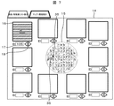
図4には、本実施例のレビューレポート作成ツールを用いて作成されるレビューレポートの完成画面を示した。図4に示される完成画面は、レビューレポート作成ツールを操作する端末のモニタに表示されるレポート作成画面であるが、装置ユーザは、この画面をプリントアウトあるいは市販のプレゼンテーションソフトウェアの操作画面に出力すれば、結果がそのままレビューレポートとなる。 FIG. 4 shows a completed screen of the review report created using the review report creation tool of this embodiment. The completed screen shown in FIG. 4 is a report creation screen displayed on the monitor of the terminal that operates the review report creation tool. The device user can print out this screen or output it to the operation screen of commercially available presentation software. In this case, the result becomes a review report as it is.
図4に示したレビューレポートは、レビューレポート作成画面(マップ・画像表示画面)14上の中央部に欠陥マップ15が表示され、その周囲に検出された欠陥の代表例を示すサムネイル画像16が複数表示された構成を有している。欠陥マップは、ウェハを模式的に示す円と、当該円上に表示された欠陥位置を示すドットにより構成される。マップ上には、サムネイル表示された欠陥を示す強調表示用ポインタが欠陥位置を示すドットの上に重ねて表示されており、更に、強調表示用ポインタとサムネイル画像の対応関係を示す矢印19も表示されている。サムネイル画像の下部に示された欠陥ID入力欄17には、欠陥IDを示す数値が表示されており、その横には、IDをスクロールさせるための矢印ボタン18が表示されている。装置ユーザは、矢印ボタン18を操作することにより、サムネイル表示させている欠陥画像の欠陥IDを変更することが可能である。
In the review report shown in FIG. 4, a
次に、図5と図6を用いて、本実施例のレビューレポート作成ツールの操作画面について説明する。レビュー結果を参照して、レビューレポートを作成するためには、装置ユーザは、まず図5に示す画像・特徴量リスト表示画面31を参照する。
Next, the operation screen of the review report creation tool of this embodiment will be described with reference to FIGS. In order to create a review report by referring to the review result, the apparatus user first refers to the image / feature amount
画像・特徴量リスト表示画面31は、外観検査装置あるいは欠陥レビュー装置から出力されたADR画像とRDC情報とを欠陥IDでソートして表示した画面であり、欠陥IDが表示される欠陥ID表示欄20,外観検査装置による検査画像22が表示される検査画像表示欄21,レビュー装置による取得画像24が表示されるレビュー画像表示欄23と、欠陥レビューが行われた製造プロセスのIDが表示されるレビューカテゴリ入力・表示欄25,検出された欠陥のRDC情報が表示される欠陥特徴量表示欄26,レビューレポートに記載するべき欠陥を選択する欠陥選択ボタン27などにより構成される。欠陥される欠陥数とRDC情報は非常に多いため、表示画面を欠陥IDの降順・昇順方向に移動するための欠陥IDスクロールバー28と横方向のスクロールバー29も用意されている。装置ユーザは、上記のスクロールバーを操作して、レビューレポートに記載するべき代表欠陥を視認し、欠陥IDを把握することができる。
The image / feature quantity
図5に示す画像・特徴量リスト表示画面31は、欠陥ID表示欄20をクリックすることで昇順または降順でソーティングされる。また、欠陥特徴量表示欄26をクリックすることで特徴量の有り・無し、あるいは特徴量の種類に沿ったソーティングも可能である。このソーティングによって、どのような種類の欠陥が、どのような特徴量をもっているのか瞬時に把握することができる。また、どのような見え方をしている欠陥が、本当に見つけたい欠陥かどうか、又は擬似欠陥なのかを確認することができる。図5の画面では、同一欠陥IDに関連する情報を横方向に並べて表示しているが、縦方向に並べても良い。
The image / feature quantity
所望のADR画像が表示されない場合には、欠陥選択ボタン27にチェックマークを付けて図5のレビューデータ出力ボタン30を押すと、チェックマークが付された欠陥IDの欠陥について、端末10(あるいは11,12)からデータベース8に欠陥レビュー画像を要求する信号が送信される。データベース8は、要求された欠陥IDのレビュー画像を検索し、存在する場合には、端末側にレビュー画像を返信する。データベース中に目的IDのレビュー画像が存在しない場合には、データベース内で当該IDに対応する座標データが生成され、図1に示す光学式レビュー装置群4またはSEM式レビュー装置群5に送られる。同時に、端末側には、「レビュー装置に問い合わせ中」のメッセージが送信される。
If the desired ADR image is not displayed, a check mark is added to the defect selection button 27 and the review
レビューレポートに記載するべき欠陥のIDが把握されると、装置ユーザは、図6に示すマップ・画像表示画面14を立ち上げる。図6に示す画面は、マップ・画像表示画面の初期画面であって、レビューレポート作成時には、この画面に表示すべき欠陥画像を次々と表示させることによってレポート作成を進めていく。画像・特徴量リスト表示画面31からマップ・画像表示画面14への切り替えは、マップ・画像表示画面タブ32をクリックすればよく、画像・特徴量リスト表示画面タブ33をクリックすると、同様に図6の表示画面から図5の表示画面に切り替わる。
When the ID of the defect to be described in the review report is grasped, the apparatus user starts up the map /
初期状態では、図6に示すレビューレポート作成画面は中央部分に欠陥マップ15が表示され、その周りにサムネイル画像表示欄34が複数配置された画面になっている。初期状態では、サムネイル画像表示欄34は空白であり、本実施例では、サムネイル画像表示欄34の配置数は10個に設定されている。装置ユーザは、まず適当なサムネイル画像表示欄34を選んで、欠陥ID入力欄17に適当な欠陥IDを入力する。欠陥IDを入力して、端末10(あるいは11,12)に備えられたキーボードのリターンキーを押すと、入力したIDに相当する欠陥のサムネイル画像がサムネイル画像表示欄34に表示される。データベースに蓄積されているADR画像や外観検査装置での取得画像の元画像はサイズが大きいため、サムネイル画像は元画像から適当に解像度を落として表示される。同時に、欠陥マップ上で表示されている当該IDの欠陥を示すドットが強調表示用ポインタ35により強調表示され、かつ当該ポインタの近傍に欠陥IDを示す数字36が表示される。図7には、図6で欠陥ID入力欄17に欠陥ID「105」を入力した場合の表示画面の例を示した。左上の像表示欄33には、欠陥ID105に対応する欠陥画像が表示されており、欠陥ID入力欄17にはIDの数値「105」が表示されている。同時に、欠陥マップ15には、入力IDに対応するドット上に強調表示用ポインタ35が表示され、その近傍には、欠陥IDを示す数字36が表示されている。表示させる欠陥を最初に選択した欠陥IDの前後で数点程度ずらしたい場合には、矢印ボタン18を操作することにより欠陥IDを前後に変える。ある欠陥がウェハ上に存在した場合、同種の欠陥はその周囲に固まって存在する場合が多いので、レビューレポート作成の都合上、欠陥マップ上での欠陥の強調表示位置を微小な距離だけ変更したい場合には、矢印ボタン18による操作が便利である。
In the initial state, the review report creation screen shown in FIG. 6 is a screen in which the
一連の欠陥検査で最初に取得される欠陥画像は外観検査装置による欠陥画像であり、データベース8には、同一IDの欠陥の画像が検査を行う時系列順に格納されるため、本実施例の欠陥レビュー支援装置では、図6のマップ・画像表示画面14で欠陥IDを入力した後に最初に表示される欠陥画像は、外観検査装置で取得された欠陥画像と設定されている。しかし、レビューレポートに掲載する画像データは、解像度の高い鮮明な画像であることが望ましい。また、上記の通り、SEM式欠陥レビュー装置では、複数種類の欠陥画像が取得されるため、レビューレポート作成ツールは、表示させる欠陥画像の種類を簡単に変更できる機能があった方が望ましい。
The defect image acquired first in a series of defect inspections is a defect image by the appearance inspection apparatus, and the images of defects with the same ID are stored in the
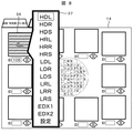
そこで、本実施例のレビュー支援装置あるいはレビューレポート作成ツールは、レビューレポート編集機能の一例として、表示させる欠陥画像の種類をプルダウンメニューにより選択する機能を備えている。表示欠陥画像の種類を変更したい場合、装置ユーザは、端末10(あるいは11,12)に備えられたマウスで、サムネイル画像表示欄34を右クリックにより選択する。すると、図8に示す表示画像種選択用プルダウンメニュー37が表示される。プルダウンメニューに表示される画像の種類は、図1に示したネットワーク7に接続された検査装置、例えば本実施例では、外観検査装置,光学式欠陥レビュー装置およびSEM式欠陥レビュー装置などから出力される画像の種類に依存する。装置ユーザは、表示された表示画像種選択用プルダウンメニュー37から適切な画像種類を選択することでこのレビューレポートに表示させる画像の種類を変更できる。なお、表示画像種選択用プルダウンメニュー37に表示させる画像の種類は装置ユーザの都合に合わせて選択することが可能である。図8に示した表示画像種選択用プルダウンメニュー37はデフォルト状態のプルダウンメニューであり、検査支援装置13に接続された検査装置が出力する全ての種類の欠陥が表示されている。この表示画像種選択用プルダウンメニュー37内の「設定」を選択すると、図9に示す表示画像種選択用プルダウンメニューに表示させる画像種の選択ウィンドウ38が表示される。表示画像種選択用プルダウンメニューに表示させる画像種の選択ウィンドウ38には、表示画像種選択ボタン39と、選択を確定するためのOKボタン40および選択を解除するためのキャンセルボタン41が表示される。装置ユーザは、表示画像種選択ボタン39を介して所望の種類の表示画像を選択する。OKボタンによる選択確定後、図10に示すように選択された欠陥画像種のみが表示画像種選択用プルダウンメニュー37に表示される。図10では、表示させる欠陥画像種として、SEM式レビュー装置の欠陥像(二番目に「D」が入っているもの)及び及びEDS分析像(EDX1及び2)を選択した例を示した。
Therefore, the review support apparatus or review report creation tool of this embodiment has a function of selecting the type of defect image to be displayed from the pull-down menu as an example of the review report editing function. When it is desired to change the type of display defect image, the device user selects the thumbnail
図6に示した初期画面に、以上説明した要領で欠陥画像を順次表示させることにより、レビューレポート作成が進行する。図11には、全てのサムネイル画像表示欄34に欠陥画像が表示された完成直前のレビューレポート作成画面(マップ・画像表示画面14)を示す。欠陥マップ15には、全ての像表示欄に表示された欠陥に対応する強調表示用ポインタ35と欠陥IDの数字35とが表示されている。この状態で、欠陥マップ15をマウスで右クリックすると、図12に示す表示情報変更・レイアウト編集用プルダウンメニュー42が表示される。この表示情報変更・レイアウト編集用プルダウンメニュー42に表示された項目中、「矢印」をマウスの右クリックなどで選択すると、欠陥マップ上に表示された強調表示用ポインタとサムネイル画像表示欄34とを結ぶ矢印が表示され、図4に示したレビューレポートが完成する。矢印は、ドットとサムネイル画像表示欄34とを結んでもよい。完成したレビューレポートは、図12のプルダウンメニュー41に含まれる「プリント」を選択することにより印刷することができる。あるいは、図4の画面を市販のプレゼンテーションソフトウェアにコピーアンドペーストすることにより、電子データとして保存することが可能である。
By sequentially displaying defect images on the initial screen shown in FIG. 6 in the manner described above, the creation of the review report proceeds. FIG. 11 shows a review report creation screen (map / image display screen 14) immediately before completion in which defect images are displayed in all thumbnail image display fields 34. The
レビューレポートの作成途中で、レビューとに掲載する欠陥画像数を増減したい場合には、上記の表示情報変更・レイアウト編集用プルダウンメニュー42を表示させ、表示項目中、「拡大」または「縮小」を選択する。いずれかの項目を選択すると、図13に示す表示画像数選択用プルダウンメニュー43が表示される。
In the middle of creating a review report, if you want to increase or decrease the number of defect images to be posted in the review, display the above-mentioned display information change / layout editing pull-
装置ユーザが表示画像数選択用プルダウンメニュー43に含まれる数字の中から適当な数字を選択すると、選択数に応じてマップ・画像表示画面14に表示される欠陥画像数が増減する。図14には、図13の表示画像数選択用プルダウンメニュー43で表示数16を選択した場合の変更後画面を示した。編集途中で表示画像数を変えたため、図14に示すマップ・画像表示画面14では、増えた分のサムネイル画像表示欄34が空欄になっている。空欄表示されたサムネイル画像表示欄34の欠陥ID入力欄17に欠陥IDを入力することにより、レビューレポート作成作業が続行される。以上説明した表示画像数の変更作業は、図6に示す欠陥ID入力開始前の段階で行うことも可能である。編集途中で表示画像数を減らす場合には、どの画像を削除するか指定する必要があるため、表示画像数選択用プルダウンメニュー43の表示項目中「減少」については、実際には欠陥ID入力開始前のレポート作成初期段階で使用される場合が多い。また、マップ・画像表示画面14上に表示されるサムネイル画像16や欠陥マップ15の枠データは画面上に表示されるオブジェクトデータであるため、マウスなどのポインティングデバイスを用いたドラッグアンドドロップ操作により、画面上で自由に移動させることができる。従って、表示画像数を編集途中で減らす場合、既に表示されたサムネイル画像をドラッグアンドドロップ操作により、図示されないゴミ箱アイコンに捨てる動作を行ってもかまわない。以上のように、プルダウンメニューによる表示画像数の設定機能とドラッグアンドドロップ操作による表示画像数の調整機能をレビューレポート作成ツールが備えることにより、ツールの操作性が向上する。
When the apparatus user selects an appropriate number from among the numbers included in the display image number selection pull-
次に、図15を用いて、以上説明したレビューレポート編集機能を実現するためのレビュー支援装置の内部動作について説明する。 Next, the internal operation of the review support apparatus for realizing the above-described review report editing function will be described with reference to FIG.
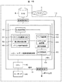
図15には、本実施例のレビューレポート作成ツールが実装された端末10の内部構成図を示した。端末10は、データベース8と共に検査支援装置13を構成し、通信ネットワーク7を介して外観検査装置群3,光学式レビュー装置群4あるいはSEM式レビュー装置群5と接続される。端末10は、図示されるような機能ブロックを実現するソフトウェアが格納されたメモリ44と、メモリ44に格納されたソフトウェアを実行するCPU45と、レビューレポート作成ツールの操作画面が表示されるユーザインタフェース46と、通信ネットワークへ接続するための通信回線端子により構成される。完成したレビューレポートの出力先デバイス(プリンタ,パーソナルコンピュータなど)も上記の通信回線端子を介して接続される。ユーザインタフェース46は、GUI画面が表示されるモニタの他、キーボードやマウスなどの入力デバイスも含むものと考える。なお、図15では、機能ブロックがメモリ上に実現されるように記載しているが、実際にはメモリ空間に格納されたプログラムをCPU45が実行することにより、上記の機能ブロックが実現されている。
FIG. 15 shows an internal configuration diagram of the terminal 10 in which the review report creation tool of this embodiment is implemented. The terminal 10 constitutes an
図15に示す機能ブロックは、データベース8を参照する際のデータ送受信の窓口となるデータベース参照部(D/B参照部)46と、レビューレポート作成ツール上に表示されるGUIでマウス入力された操作ポインタの位置検出を行い、それがどのような命令に相当するかを解析するポインタ動作解析部48と、GUI表示する表示画面の全般的な制御を行う表示制御部49と、作成されたレビューレポートを外付けプリンタに出力する際やあるいは市販のプレゼンテーションソフトウェアに出力する際のフォーマット変換を実行する出力制御部50とを含んで構成されている。ここで「操作ポインタ」とは、図5の画像・特徴量リスト表示画面31や図6のマップ・画像表示画面の両方で表示される、全GUI画面共通の操作ポインタのことであり、欠陥マップ上に表示される強調表示用ポインタとは区別される。ポインタ動作解析部48は、更に操作ポインタの位置検出を行うポインタ位置検出部51と、操作ポインタの移動先の位置情報とGUI表示されたオブジェクトデータの表示位置との対応関係を参照して、マウス入力された操作ポインタの動作の意味を解析する要求動作解析部52とを含んで構成される。また、表示制御部49は、欠陥マップのGUI表示を行うマップ描画部53と、マップ周囲以外のオブジェクトデータ、例えばサムネイル画像や各種プルダウンメニューの表示を行うオブジェクト表示部54とを含んで構成される。
The functional blocks shown in FIG. 15 are a database reference unit (D / B reference unit) 46 serving as a window for data transmission / reception when referring to the
例えば、図6に示す欠陥マップを表示する場合、まずマップ描画部53がデータベース参照部47にマップ描画に必要な情報を取得するよう指令を送信する。データベース参照部47は、図3に示すテーブルから図6のマップ描画に必要なフィールド、すなわちデータベース欠陥IDフィールド,x座標フィールド,y座標フィールド,第1欠陥画像フィールドというフィールドを選択して、通信ネットワークで使用されるフォーマットのパケットを生成し、データベース8に送信する。データベース8は要求された情報をデータベース参照部47に返信し、データベース参照部47は返信されたパケットから必要な情報を取り出し、メモリ44の空き領域(図示せず)に格納した後、データを格納したメモリアドレスをマップ描画部53に送信する。
For example, when the defect map shown in FIG. 6 is displayed, the
マップ描画部53は、取得した欠陥のx,y座標の情報をGUI画面上での表示位置に変換し、ウェハを示す画像情報(例えば、ウェハの輪郭線情報やチップを示す矩形情報など)と共にユーザインタフェース46に表示する。同時に、オブジェクト表示部54は、欠陥マップ15の周囲にサムネイル画像表示欄34,欠陥ID入力欄17および矢印ボタン18を表示させる。欠陥ID入力欄17にIDが入力されると、ポインタ位置検出部51がポインタに何らかの変化が生じたことを検出し、ポインタの確定位置を解釈して欠陥ID入力欄17への入力動作があったことを検出する。要求動作解析部52は欠陥ID入力欄17への入力情報を取得してオブジェクト表示部54に伝達する。オブジェクト表示部54は、メモリに格納されたデータベース8からのダウンロードデータを参照し、欠陥IDを検索キーとしてサムネイル画像表示欄34に表示させる画像データを検索する。検索の結果、画像データがメモリ内に存在すれば、メモリ内に存在する画像データから適当に解像度を落としたサムネイル用画像データを生成し、サムネイル画像表示欄34に重畳させて表示する。元画像のデータが存在しない場合はデータベース参照部47に画像取得要求を送信する。
The
一方、要求動作解析部52の解析結果はマップ描画部53にも伝送される。これにより、マップ描画部53は欠陥ID入力欄17へIDが入力された状態の欠陥(とその欠陥のID)を把握でき、欠陥マップ上の対応する位置に欠陥の強調表示用ポインタと欠陥IDとを表示することが可能となる。
On the other hand, the analysis result of the requested
図8,図10あるいは図12に示すプルダウンメニューを表示する際には、プルダウンメニュー表示のトリガーとなるマウス動作があったかどうかをポインタ位置検出部51が検出し、更に、要求動作解析部52が当該マウス動作を解析し、結果をオブジェクト表示部54に伝送する。オブジェクト表示部54は、伝送された結果に応じて、各種のプルダウンメニューを表示させる。所定のプルダウンメニューが表示中であるという情報は、ポインタ動作解析部48に伝送され、これにより、ポインタ位置検出部51および要求動作解析部52は、プルダウンメニューの選択動作を解釈することが可能となる。以上のように、マウスなどポインティングデバイスの分析を担うポインタ動作解析部48と、欠陥マップや各種サムネイル画像の表示を担う表示制御部49が保持している画面の状態情報が、現在表示されている画面の状態情報に同期しているため、レビューレポートのレイアウト編集機能がレビューレポートの作成画面上で実現される。
When the pull-down menu shown in FIG. 8, FIG. 10, or FIG. 12 is displayed, the pointer
図13で表示させるサムネイル画像数を変更した場合、サムネイル画像の表示サイズが自動変更されるが、表示サイズおよび表示位置変更の演算処理もオブジェクト表示部54により実行される。
When the number of thumbnail images to be displayed in FIG. 13 is changed, the display size of the thumbnail images is automatically changed, but the calculation processing for changing the display size and the display position is also executed by the
実際には、図5に示す画像・特徴量リスト表示画面31の画面を表示する時点でデータベース8へのアクセスは発生しているので、その時点で図6を表示するために必要な情報をデータベース8に要求する場合が多い。すなわち、図5の画像・特徴量リスト表示画面31画面を表示するためには欠陥座標の位置情報は不要であるが、その時点で欠陥座標の位置情報も取得しており、かつ存在する欠陥画像データも全てデータベース8からダウンロードしている場合が多いため、図6以降ではデータベース8への画像要求は不要である場合が多い。
Actually, access to the
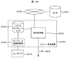
以上説明した本実施例のレビューレポート作成ツールの優位性について説明するために、テンプレート型レビューレポート作成ツールが実装された端末あるいはレビュー支援装置の内部構成について説明する。図24には、テンプレート型レビューレポート作成ツールが実装された端末の内部構成図を示した。図15に示した端末2400は、本実施例の端末10と同様、データベース2401に通信ネットワーク2402を介して接続されている。装置ユーザは、ユーザインタフェース2403を介してレビューレポートを編集し、編集結果は、端末内のメモリやハードディスクなどに格納されたレポートテンプレートデータベース2404にか記憶される。テンプレート編集制御部2405は、ユーザインタフェース2403に表示させる表示画面を作成する。表示制御部2406は、テンプレートデータベース2404に記憶されたテンプレートを参照して、データベース2401から取得した情報をテンプレートに合成してレビューレポートを作成する。レビューレポートに記載する情報は、ウェハIDやロット番号などの情報を元に、関連する情報をデータベース2401から全部取得し、その中からテンプレートを参照して抽出する。
In order to explain the superiority of the review report creation tool of the present embodiment described above, the internal configuration of the terminal or the review support apparatus in which the template type review report creation tool is mounted will be described. FIG. 24 shows an internal configuration diagram of a terminal in which the template type review report creation tool is implemented. A terminal 2400 shown in FIG. 15 is connected to a
以上の説明で分かるように、テンプレート型のレビューレポート作成ツールの場合、一旦テンプレートを決めてしまうと、サムネイル画像や矢印の表示位置の調整をするためには、再度テンプレート編集画面に戻って作業を行う必要がある。しかし、レビューレポートのレイアウトは、レポート作成過程で装置ユーザの意図に応じて変更されうるものである。よって、テンプレート型のレビューレポート作成ツールの場合、レビューレポートの完成画面に到達するまでに、テンプレート編集〜合成画面によるレポート画面の確認〜テンプレート編集画面に戻っての再編集、という煩雑な作業を繰り返す必要があり、レポート作成に多大な時間を要していた。 As can be seen from the above description, in the case of the template-type review report creation tool, once the template has been decided, to adjust the display position of thumbnail images and arrows, return to the template editing screen and work again. There is a need to do. However, the layout of the review report can be changed according to the intention of the device user in the report creation process. Therefore, in the case of a template-type review report creation tool, until the completion screen of the review report is reached, the complicated work of template editing, confirmation of the report screen using the composite screen, and re-editing back to the template editing screen is repeated. It took a lot of time to create a report.
本実施例のレビューレポート作成ツールの場合、レビューレポート作成の操作画面上でレビューレポートのレイアウトを変更できる編集機能を有しているため、レビューレポート作成の手数が大幅に低減される。本実施例の効果を示すため、図16には、レビューレポート作成に要する時間を従来技術と本発明とで対比して示した。図16は、欠陥レビュー装置によるレビュー時間をレポート作成時間も含めて表示した円グラフであり、横軸が時間を示す。従来技術と本発明とでは、レポート作成時間が従来の1/4と大幅に短縮されていることが分かる。 In the case of the review report creation tool of this embodiment, the review report creation tool has an editing function that can change the layout of the review report on the operation screen for creating the review report. In order to show the effect of the present embodiment, FIG. 16 shows the time required for creating the review report in comparison with the prior art and the present invention. FIG. 16 is a pie chart in which the review time by the defect review apparatus is displayed including the report creation time, and the horizontal axis indicates the time. It can be seen that the report creation time is significantly shortened to ¼ of the conventional technique and the present invention.
以上、本実施例のレビューレポート作成ツールにより、大量の画像データを用いた解析や整理・まとめが容易なレビュー支援装置を実現することができる。 As described above, the review report creation tool of the present embodiment can realize a review support device that can easily analyze, organize, and summarize using a large amount of image data.
実施例1では、欠陥IDを手入力することによりレビューレポートを作成することが可能なレビューレポート作成ツールについて説明したが、本実施例では、より操作性の向上されたレビューレポート作成ツールの構成について説明する。 In the first embodiment, the review report creation tool capable of creating the review report by manually inputting the defect ID has been described. However, in this embodiment, the configuration of the review report creation tool with improved operability is described. explain.
最初に、本実施例のレビューレポート作成装置が実装されるレビュー支援装置とその周辺に配置される装置の関係を示す全体図を図17に示す。図17に示すレビュー支援装置55は、欠陥レビューSEM56にレビューレポート作成ツールが実装された端末57とにより構成される。また、レビュー支援装置55は、通信ネットワーク58を介してデータベース59,外観検査装置61,光学式レビュー装置62に相互接続されている。実施例1と同様に、外観検査装置61,光学式レビュー装置62および欠陥レビューSEM56で撮像された画像は、データベース59に蓄積され、必要に応じて端末57により読み出される。ワークステーション60は、実施例1のそれと同様、データベースに格納する画像情報を、外観検査装置61,光学式レビュー装置62および欠陥レビューSEM56で取得された画像から抽出するフィルター機能を備える。なお、データベース59に格納されるデータの配列構造も図3とほぼ同一であるものとする。
First, FIG. 17 shows an overall view showing the relationship between a review support device in which the review report creation device of this embodiment is mounted and devices arranged in the vicinity thereof. The
欠陥レビューSEM56は、ウェハに一次荷電粒子線を照射して発生する二次荷電粒子信号として出力する荷電粒子光学鏡筒63と、ウェハを載置する試料ステージ65を格納する真空試料室64,荷電粒子光学鏡筒63および真空試料室64の全体動作を制御する全体制御部66および撮像画像を用いて取得された欠陥の分類を行う画像処理部67とにより構成される。荷電粒子光学鏡筒63は、更に、一次電子ビームを発生する電子源68,電子源で発生した電子ビームのビーム電流量を制御するための上部・下部コンデンサレンズ69,71およびビーム電流絞り70,電子ビームを試料上に走査する走査偏向器72,一次電子ビームの照射により発生する二次荷電粒子を光軸外に反射させる反射板73,走査偏向器により走査される電子ビームを試料上に集束させる対物レンズ74,反射板で反射された二次荷電粒子のうち紙面左側に反射された反射電子を検出する左陰影像検出器75,略同紙面右側に反射された反射電子を検出する右陰影像検出器76,二次電子像の形成信号を出力する二次電子検出器77などにより構成される。
The
画像処理部67はデータベース59を参照して、欠陥レビューが完了していない欠陥のIDと欠陥位置情報とを取得する。これら欠陥IDと欠陥位置情報は、外観検査装置61から直接送信される場合もある。端末57の内部構成は、図15で説明した内容と同一であるので、説明は省略する。
The
次に、図6,図18および図19を用いて、本実施例のレビューレポート作成ツールの操作画面について説明する。なお、説明の都合上、レビューレポートの完成画面は図4に示す画面と同じであるものとする。装置ユーザは、最初にレビューレポート作成画面の初期画面を表示させる。初期画面は、図6に示す実施例1の初期画面と同様である。本実施例の場合、レビューレポート作成画面の初期画面に表示される欠陥マップ上に操作ポインタをかざす(マウスなどのポインティングデバイスで、欠陥マップ上のドットにポインタを移動させる)と、当該欠陥のサムネイル画像と欠陥IDとを表示する吹き出し画面が表示される。例えば、図18には、上記の吹き出し画面が表示された状態のマップ・画像表示画面78を示した。図18では、IDが105の欠陥に相当する第1のサムネイル画像79が既に表示されており、欠陥マップ80上でも欠陥ID105の欠陥位置が強調表示用ポインタ81により強調表示されている。また、その近傍には欠陥ID82である数値「105」も表示されている。
Next, the operation screen of the review report creation tool of the present embodiment will be described with reference to FIG. 6, FIG. 18, and FIG. For the convenience of explanation, it is assumed that the review report completion screen is the same as the screen shown in FIG. The device user first displays the initial screen of the review report creation screen. The initial screen is the same as the initial screen of the first embodiment shown in FIG. In this embodiment, when the operation pointer is placed over the defect map displayed on the initial screen of the review report creation screen (the pointer is moved to a dot on the defect map with a pointing device such as a mouse), a thumbnail of the defect is displayed. A balloon screen displaying the image and the defect ID is displayed. For example, FIG. 18 shows a map /
装置ユーザが、次に表示させるサムネイル画像を選択するために、欠陥マップ上の適当なドットに操作ポインタをかざすと、第2のサムネイル画像84と欠陥ID85とを含む吹き出し画面83がポップアップ表示される。装置ユーザは、マウスなどのポインティングデバイスを操作して、吹き出し画面83に表示された第2のサムネイル画像84を、マップ・画像表示画面78に表示された複数の像表示欄のうち所望の像表示欄86にドラッグアンドドロップ操作を行う。これにより、吹き出し画面83に表示された第2のサムネイル画像84が像表示欄86に貼り付けることができる。同時に、像表示欄86の欠陥ID入力欄87には、ドラッグアンドドロップ操作を行った欠陥画像に対応する欠陥IDが自動表示される。欠陥マップ80上にも、選択されたサムネイル画像に対応する欠陥位置が強調表示用ポインタ81により強調表示され、かつ欠陥ID値「154」も表示される。図19には、図18の吹き出し画面84から第2のサムネイル画像をドラッグアンドドロップ操作した直後の表示画面を示した。
When the device user holds the operation pointer over an appropriate dot on the defect map in order to select a thumbnail image to be displayed next, a
また、欠陥ID入力欄87横の矢印ボタン88を押すと欠陥ID入力欄87に表示される欠陥ID値がボタンを押した回数に応じて変更される。同時に、像表示欄86に表示される画像と欠陥マップ80上に表示された強調表示用ポインタ81の表示位置とが、IDの変化に応じて変更される。
When the
更にまた、マップ・画像表示画面78に表示させているサムネイル画像を削除する場合は、その画像をクリックして図示されないゴミ箱アイコンに移動させるドラッグアンドドロップ操作を行う。また、各欠陥画像を他の画像にドラッグアンドドロップすることで、画像表示位置を交換することも可能である。
Furthermore, when deleting a thumbnail image displayed on the map /
以上の要領で、欠陥マップ上で操作ポインタを移動し、吹き出し画面を次々と表示させ、所望のサムネイル画像を順次貼り付けることにより、レビューレポートの作成が進行する。 As described above, the operation pointer is moved on the defect map, the balloon screens are displayed one after another, and a desired thumbnail image is pasted in sequence, thereby creating a review report.
次に、本実施例の端末57の内部動作について図15を参照して説明する。欠陥マップやサムネイル画像を表示する際の端末内部の動作は、実施例1と同様であるので、ここでは、吹き出し画面に表示された画像のコピーアンドペースト操作時の内部動作について説明する。 Next, the internal operation of the terminal 57 of this embodiment will be described with reference to FIG. Since the internal operation of the terminal when displaying the defect map and the thumbnail image is the same as that of the first embodiment, the internal operation during the copy and paste operation of the image displayed on the balloon screen will be described here.
装置ユーザのポインティングデバイス操作により、図18に示す欠陥マップ上の任意のドット上に操作ポインタが移動されると、ポインタ位置検出部51は、操作ポインタの現在の表示位置を検出し、要求動作解析部52に伝送する。要求動作解析部52は、伝送された操作ポインタの現在の表示位置が欠陥マップ80上に表示されたドットの表示位置と同じであることを検出して吹き出し画面83の表示要求と解釈する。要求動作解析部52は、更に、解釈結果である「表示要求」を欠陥ID値の情報とともに、表示制御部49に伝送する。マップ描画部53は、伝送された欠陥IDに対応するドットの近傍に上記の吹き出し画面83をポップアップ表示させ、同時に、強調表示用ポインタ81も表示させる。オブジェクト表示部54は、ポップアップ表示された吹き出し画面83内にサムネイル画像と欠陥ID値とをオブジェクトデータとして表示させる。
When the operation pointer is moved onto an arbitrary dot on the defect map shown in FIG. 18 by the pointing user operation of the apparatus user, the pointer
次に、吹き出し画面83内に表示されたオブジェクトデータであるサムネイル画像が像表示欄86にドラッグアンドドロップ操作されると、ポインタ位置検出部51がこの動作を検出し、要求動作解析51に伝送する。要求動作解析51は、このドラッグアンドドロップ操作が、欠陥ID154の欠陥画像の像表示欄86への貼り付け動作と解釈し、表示制御部49に伝送する。オブジェクト表示部54は、像表示欄86へ欠陥ID154の欠陥画像を表示し、併せて、欠陥ID入力欄87に欠陥ID値「154」を表示させる。吹き出し画面83は、操作ポインタが欠陥ID154の位置から移動されない限り表示されたままであるが、操作ポインタの操作が一定時間以上無かった場合、タイムアウトで吹き出し画面83の表示を終了するように装置を構成しても良い。
Next, when a thumbnail image that is object data displayed in the
欠陥マップ上に表示されているドット数が多い場合には、欠陥マップ上で操作ポインタを動かしてドットを選択する場合に支障が生じる場合がある。そのような場合のため、本実施例のレビューレポート作成ツールは欠陥マップの一部を拡大表示する機能を有しており、装置ユーザは、拡大表示された領域からサムネイル表示させる欠陥を選択することができる。欠陥マップを拡大表示させる場合には、装置ユーザは、操作ポインタを欠陥マップ80上でドットが表示されていない適当な領域に移動させ、ポインティングデバイスを操作(マウスの右クリックなど)する。すると、実施例1の図12に示すような表示情報変更・レイアウト編集用プルダウンメニュー42が表示され、表示項目の中から「拡大」を表示すると、図20に示すような欠陥マップの拡大図がマップ・画像表示画面78中央部に表示される。拡大表示されても、強調表示用ポインタ81や欠陥ID入力欄87に表示される欠陥ID値の情報は、欠陥マップ拡大図89にそのまま表示される。また、欠陥マップ拡大図89の表示位置を移動させるため、拡大マップ表示位置移動スクロールバー90も欠陥マップ拡大図89に併せて表示される。*この黄色マーカ箇所(ナントカ用スクロールバー)に適当に名前をつけてください。拡大表示された欠陥マップの表示サイズを元に戻す場合には、マウス操作により表示情報変更・レイアウト編集用プルダウンメニュー42を再度表示させ、表示項目の中から「縮小」を選択すればよい。
When the number of dots displayed on the defect map is large, there may be a problem in selecting a dot by moving the operation pointer on the defect map. For such a case, the review report creation tool of the present embodiment has a function of enlarging and displaying a part of the defect map, and the apparatus user selects a defect to be displayed as a thumbnail from the enlarged area. Can do. When the defect map is enlarged and displayed, the apparatus user moves the operation pointer to an appropriate area where no dot is displayed on the
マップ・画像表示画面78には、欠陥マップの代わりに、マップの変わりに画像一覧91を表示することも可能である。「画像一覧」とは、欠陥マップ80に表示されている全ドットに対応する欠陥画像を欠陥ID順に並べて表示したものである。図3に示すように、同一の欠陥IDに対して複数種類の欠陥画像が存在するため「画像一覧」に表示される欠陥画像には、同一IDの欠陥画像が複数含まれることになる。
On the map /
画像一覧を表示する場合には、ポインティングデバイスの操作により、図12に示すような表示情報変更・レイアウト編集用プルダウンメニュー42を呼び出し、表示項目の中から「画像一覧」を選択する。図21には、画像一覧が表示された状態のマップ・画像表示画面78を示す。図21に表示された画像一覧91では、欠陥ID入力欄87へ欠陥IDが入力されている欠陥画像がハイライト表示92され、装置ユーザはどの画像がサムネイル表示されているかたちどころに理解することができる。また、画像一覧91に表示された表示画像選択用スクロールバー93を操作することにより、画像一覧91に表示される欠陥画像をスライドさせることができる。装置ユーザは、画像一覧91に表示された欠陥画像の中から所望の画像を選択し、所望の像表示欄にドラッグアンドドロップ操作することで、像表示欄に所望の欠陥画像をサムネイル表示することができる。このドラッグアンドドロップ操作は、像表示欄が空白であっても既にサムネイル画像が表示されていても有効である。画像一覧の表示を欠陥マップ表示に切り替える場合には、図12に示すような表示情報変更・レイアウト編集用プルダウンメニュー42を呼び出し、表示項目の中から「マップ」を選択することにより、欠陥マップ表示に切り替えることができる。
When displaying an image list, a display information change / layout editing pull-
以上説明した欠陥マップの拡大・縮小表示動作あるいは欠陥画像の一覧表示、あるいはプルダウンメニューの表示などの各種動作も、図15に示すポインタ動作解析部48が、マウスによる操作ポインタの動作を検出・解析し、表示制御部49に伝送することにより実現される。
In various operations such as the defect map enlargement / reduction display operation, defect image list display, or pull-down menu display described above, the pointer
以上のように、欠陥マップによるサムネイル画像選択と、画像一覧によるサムネイル画像選択とを切り替えることにより、欠陥マップによる欠陥分布の把握容易性と、画像一覧による欠陥画像の形状の視認性とを両立することが可能となり、どちらか一方しか表示できない場合に比べて、レビューレポート作成時の操作性が更に向上する。 As described above, by switching between thumbnail image selection based on the defect map and thumbnail image selection based on the image list, both the ease of grasping the defect distribution based on the defect map and the visibility of the shape of the defect image based on the image list are compatible. As compared with the case where only one of them can be displayed, the operability when creating the review report is further improved.
更にまた、実施例1の操作と同様に、既にサムネイル画像が表示されている像表示欄であっても、欠陥ID入力欄87に所望の欠陥IDを入力すると像表示欄に新たに入力した欠陥IDの欠陥画像が表示される。従って、本実施例のレビューレポート作成ツールにおいては、装置ユーザは、欠陥ID入力欄87への欠陥IDのマニュアル入力によるサムネイル画像選択と、欠陥マップあるいは画像一覧からの画像のドラッグアンドドロップ操作によるサムネイル画像選択との2つの選択方法を切り替えて使用することができる。これにより、レポートに表示させる適切な画像の抽出・選択の利便性が向上し、ひいては必要な情報を含むレポートの作成時間がより短時間化し、歩留まり向上までの所要時間が短縮する。
Furthermore, as in the operation of the first embodiment, even if the thumbnail display is already displayed in the image display column, if a desired defect ID is input in the defect
図22には、画像一覧表示に表示させる欠陥画像を絞り込むためのデータフィルタリングウィンドウ100を示した。本画面は、図12に示された表示情報変更・レイアウト編集用プルダウンメニューに含まれる「フィルタリング」項目を選択することにより、「マップ・画像表示画面78」からのポップアウトウィンドウとして表示される。図22に示すデータフィルタリングウィンドウ100には、欠陥種別情報が表示される欠陥種別ウィンドウ101,欠陥種別情報以外の欠陥特徴量情報が表示されるRDCウィンドウ102などが表示される。装置ユーザは、マウスやキーボードなどの入力デバイスを使用して、欠陥種別ウィンドウ101に表示された欠陥種別リストから所望の種別の欠陥を選択する。あるいはRDCウィンドウ102内に表示された欠陥特徴量入力欄103に適当な値を入力する。例えば、「MaxGlDiff」入力欄(最大グレーレベル差入力欄)であれば、適当なグレーレベル差の諧調値を入力する。「Polarity」入力欄(極性入力欄)であれば、プラスまたはマイナスの符号を入力する。その後、確定ボタン105を押すと、ユーザの選択した欠陥種別あるいはRDC情報に対応する欠陥画像のみが図21に示す画像一覧に表示される。「全て選択」ボタン104を押せば、全ての欠陥画像が選択される。また、欠陥マップであれば、ユーザの選択した欠陥種別あるいはRDC情報に対応する欠陥に対応するドットのみが欠陥マップ上に表示される。キャンセルボタン106を押すと設定は解除される。
FIG. 22 shows a
以上のように、レビューレポート作成画面にRDC情報の選択条件設定機能を持たせることにより、GUI画面に表示させる欠陥画像の種類をレビューレポート作成者の意図に応じて絞り込むことが可能となるため、レビューレポートに表示させたい欠陥に短時間で且つ簡単にたどり着くことが可能となる。以上の表示制御も、図15に示すポインタ動作解析部48と表示制御部49との共同処理によって実現される。
As described above, since it is possible to narrow down the types of defect images to be displayed on the GUI screen according to the intention of the review report creator by providing a selection condition setting function for RDC information on the review report creation screen. It is possible to quickly and easily reach the defect to be displayed in the review report. The above display control is also realized by joint processing of the pointer
また、図18〜図21に示されるサムネイル画像の拡大画像を表示させたい場合がある。これは、微細な欠陥の場合、画像を拡大して欠陥部を大きく表示して確認したい場合が多いためである。このような場合、サムネイル画像をダブルクリックすると、図23に示す画像拡大表示・欠陥種別コード入力ウィンドウ107が表示され、レビューレポート作成画面(マップ・画像表示画面78)に表示させたサムネイル画像を高精細な拡大画像で確認することができる。また、画像拡大表示・欠陥種別コード入力ウィンドウ107には、スライドボタン108も表示されており、「Prev」または「Next」の各ボタンを操作することで、表示される欠陥画像が欠陥IDに従って変化する。
In some cases, it is desired to display an enlarged image of the thumbnail image shown in FIGS. This is because, in the case of a fine defect, there are many cases where it is desired to enlarge the image and display the defect portion for confirmation. In such a case, when the thumbnail image is double-clicked, the image enlargement display / defect type
実施例1で説明したように、サムネイル画像は元画像から適当に解像度を落として表示されているため、上記のダブルクリックにより画像拡大表示・欠陥種別コード入力ウィンドウ107が呼び出されると、図15に示すポインタ動作解析部は、ダブルクリックされたマップ・画像表示画面78上の位置情報から選択された欠陥のIDを算出しオブジェクト表示部54に伝達する。オブジェクト表示部54は、伝達された欠陥IDの情報を元にメモリ44の空き領域に格納された欠陥画像のデータを参照して、解像度を落とさずに画像拡大表示・欠陥種別コード入力ウィンドウ107上に表示する。
As described in the first embodiment, since the thumbnail image is displayed with the resolution appropriately reduced from the original image, when the image enlargement display / defect type
図23に示されるように、画像拡大表示・欠陥種別コード入力ウィンドウ107には、ダブルクリックにより選択された欠陥IDを持つ欠陥画像が全て表示される。表示させる欠陥画像を絞り込みたい場合、画像拡大表示・欠陥種別コード入力ウィンドウ107上に表示されている欠陥種別コード入力欄109に欠陥種別を示すコード情報を入力することにより、ウィンドウ上に表示させる欠陥画像を選択することができる。この状態でスライドボタン108を操作すると、表示される欠陥画像はやはり欠陥IDに従って変化する。このようにすることで、微細な欠陥の確認が容易になり、目視による欠陥の確認時間が短縮される。
As shown in FIG. 23, in the enlarged image display / defect type
以上の説明は、レビュー支援装置が、欠陥レビューSEMに接続されたレビューレポート作成端末と欠陥レビューSEMにより構成されることを前提として行ったが、本実施例のドラッグアンドドロップ操作によるレビューレポート作成方法は、図1に示すようにデータベースとレビューレポート作成端末から構成される検査支援装置あるいはレビュー支援装置に対しても適用することが可能である。 The above description has been made on the assumption that the review support apparatus includes a review report creation terminal connected to the defect review SEM and the defect review SEM. However, the review report creation method by the drag-and-drop operation according to the present embodiment is described. As shown in FIG. 1, it can also be applied to an examination support apparatus or a review support apparatus that includes a database and a review report creation terminal.
1 クリーンルーム
2 半導体製造装置
3 外観検査装置群
4 光学式レビュー装置群
5 SEM式レビュー装置群
6 検品装置
7,58 通信ネットワーク
8,59 データベース
9,60 ワークステーション
10〜12,57 端末
13 実施例1の欠陥検査支援装置
14 実施例1のマップ・画像表示画面
15 欠陥マップ
16 サムネイル画像
17,87 欠陥ID入力欄
18,88 矢印ボタン
19 矢印
20 欠陥ID表示欄
21 検査画像表示欄
22 外観検査装置による検査画像
23 レビュー画像表示欄
24 レビュー装置による取得画像
25 レビューカテゴリ入力・表示欄
26 欠陥特徴量表示欄
27 欠陥選択ボタン
28 欠陥IDスクロールバー
29 横方向のスクロールバー
30 レビューデータ出力ボタン
31 画像・特徴量リスト表示画面
32 マップ・画像表示画面タブ
33 画像・特徴量リスト表示画面タブ
34 サムネイル画像の画像表示欄
35 強調表示用ポインタ
36 欠陥IDを示す数字
37 表示画像種選択用プルダウンメニュー
38 表示画像種選択用プルダウンメニューに表示させる画像種の選択ウィンドウ
39 表示画像種選択ボタン
40 OKボタン
41 キャンセルボタン
42 表示情報変更・レイアウト編集用プルダウンメニュー
43 表示画像数選択用プルダウンメニュー
44 メモリ
45 CPU
46 ユーザインタフェース
47 データベース参照部
48 ポインタ動作解析部
49 表示制御部
50 出力制御部
51 ポインタ位置検出部
52 要求動作解析部
53 マップ描画部
54 オブジェクト表示部
55 実施例2の欠陥レビュー支援装置
56 欠陥レビューSEM
61 外観検査装置
62 光学式レビュー装置
63 荷電粒子光学鏡筒
64 真空試料室
65 試料ステージ
66 全体制御部
67 画像処理部
68 電子源
69 上部コンデンサレンズ
70 ビーム電流絞り
71 下部コンデンサレンズ
72 走査偏向器
73 反射板
74 対物レンズ
75 左陰影像検出器
76 右陰影像検出器
77 二次電子検出器
78 実施例2のマップ・画像表示画面
79 第1のサムネイル画像
80 欠陥マップ
81 強調表示用ポインタ
82,85 欠陥ID
83 吹き出し画面
84 第2のサムネイル画像
86 像表示欄
89 欠陥マップ拡大図
90 拡大マップ表示位置移動スクロールバー
91 画像一覧
92 ハイライト表示
93 表示画像選択用スクロールバー
100 データフィルタリングウィンドウ
101 欠陥種別ウィンドウ
102 RDCウィンドウ
103 欠陥特徴量入力欄
104 「全て選択」ボタン
105 確定ボタン
106 キャンセルボタン
107 画像拡大表示・欠陥種別コード入力ウィンドウ
108 スライドボタン
109 欠陥種別コード入力欄
DESCRIPTION OF
46
61
83
Claims (14)
前記外観検査装置ないし前記観察装置に結線される通信回線が接続され、かつ前記複数の欠陥の位置情報と画像情報とを取り込むための通信回線端子と、
前記欠陥の位置情報と画像情報とを処理する演算手段と、
前記演算手段の処理結果が表示されるモニタとを有し、
当該モニタ上には、
前記被検査試料上における前記複数の欠陥の位置を示す欠陥マップと、当該複数の欠陥のうち、少なくとも2つ以上の欠陥のサムネイル画像と、当該2つ以上の欠陥にそれぞれ対応する識別子情報と、前記欠陥マップ、サムネイル画像あるいは識別子情報を指定するための操作ポインタとを含むレビューレポート作成画面が表示され、
かつ、前記サムネイル画像は、前記表示画面上での配置位置がそれぞれ独立に変更可能なように、前記レビューレポート作成画面上に表示されることを特徴とするレビュー支援装置。 In a review support device that is used in connection with a defect review device having a review function for a plurality of defects existing in a sample to be inspected,
A communication line connected to the visual inspection apparatus or the observation apparatus, and a communication line terminal for capturing positional information and image information of the plurality of defects,
Arithmetic means for processing the defect position information and image information;
A monitor on which the processing result of the computing means is displayed;
On the monitor,
A defect map indicating positions of the plurality of defects on the sample to be inspected, thumbnail images of at least two or more defects among the plurality of defects, identifier information corresponding to the two or more defects, A review report creation screen including an operation pointer for designating the defect map, thumbnail image or identifier information is displayed,
The thumbnail image is displayed on the review report creation screen so that the arrangement position on the display screen can be changed independently.
前記外観検査装置に接続される通信回線が接続され、かつ前記複数の欠陥の位置情報と画像情報とを取り込むための通信回線端子と、
前記欠陥の位置情報と画像情報とを処理する演算手段と、
前記欠陥レビューの結果を要約したレビューレポートを作成するための操作画面が表示されるモニタとを有し、
前記演算手段は、前記レビューレポートのレイアウト編集機能が実現されるように、前記操作画面に表示される画像データの表示を変更することを特徴とするレビュー支援装置。 In a review support device that is used in connection with a defect review device having a review function for a plurality of defects existing in a sample to be inspected,
A communication line terminal connected to the appearance inspection apparatus, and a communication line terminal for capturing position information and image information of the plurality of defects;
Arithmetic means for processing the defect position information and image information;
A monitor on which an operation screen for creating a review report summarizing the results of the defect review is displayed;
The review support device, wherein the calculation means changes a display of image data displayed on the operation screen so that a layout editing function of the review report is realized.
前記操作画面上には、
前記被検査試料上における前記複数の欠陥の位置を示す欠陥マップと、当該複数の欠陥のうち、少なくとも2つ以上の欠陥のサムネイル画像と、当該2つ以上の欠陥にそれぞれ対応する識別子情報とが表示され、
更に、前記演算手段は、
前記サムネイル画像の前記操作画面上での配置位置がそれぞれ独立に変更可能なように、当該サムネイル画像を前記画面上に表示することを特徴とするレビュー支援装置。 The review support apparatus according to claim 2,
On the operation screen,
A defect map indicating positions of the plurality of defects on the sample to be inspected, thumbnail images of at least two or more defects among the plurality of defects, and identifier information respectively corresponding to the two or more defects. Displayed,
Further, the calculation means includes:
A review support apparatus, wherein the thumbnail image is displayed on the screen so that the arrangement position of the thumbnail image on the operation screen can be independently changed.
前記演算装置は、前記サムネイル画像を前記操作ポインタの移動先に移動させることを特徴とするレビュー支援装置。 The review support apparatus according to claim 2,
The review support device, wherein the arithmetic device moves the thumbnail image to a destination of the operation pointer.
前記演算装置は、前記操作ポインタによる指示を契機として、前記操作画面上に表示するサムネイル画像の個数を変更するためのプルダウンメニューを表示させることを特徴とするレビュー支援装置。 The review support apparatus according to claim 4,
The review support device, wherein the arithmetic device displays a pull-down menu for changing the number of thumbnail images to be displayed on the operation screen in response to an instruction from the operation pointer.
前記サムネイル画像の個数の変更に応じて、前記サムネイル画像の前記操作画面上での大きさが変更されることを特徴とするレビュー支援装置。 The review support apparatus according to claim 4,
The review support apparatus, wherein a size of the thumbnail image on the operation screen is changed according to a change in the number of thumbnail images.
前記欠陥マップ上では、当該サムネイル画像に対応する欠陥位置が、他の欠陥位置とは区別されるように表示されることを特徴とするレビュー支援装置。 The review support apparatus according to claim 4,
A review support apparatus, wherein a defect position corresponding to the thumbnail image is displayed on the defect map so as to be distinguished from other defect positions.
前記識別子情報を変更するための変移ボタンが表示されることを特徴とするレビュー支援装置。 The review support apparatus according to claim 4,
A review support apparatus, wherein a transition button for changing the identifier information is displayed.
前記ポインタを前記サムネイル画像上に移動させると、
当該サムネイル画像と識別子の同じ欠陥について、撮像方法の異なる複数の欠陥画像を選択するためのプルダウンメニューが前記操作画面上に表示されることを特徴とするレビュー支援装置。 The review support apparatus according to claim 4,
When the pointer is moved over the thumbnail image,
A review support apparatus, wherein a pull-down menu for selecting a plurality of defect images having different imaging methods is displayed on the operation screen for the defect having the same identifier as the thumbnail image.
前記プルダウンメニューには、当該プルダウンメニューに含まれる欠陥画像の種類を調整するための設定ボタンもあわせて表示されることを特徴とするレビュー支援装置。 The review support apparatus according to claim 9,
The review support apparatus is characterized in that a setting button for adjusting the type of defect image included in the pull-down menu is also displayed in the pull-down menu.
前記検査マップ上に表示される欠陥位置に前記ポインタを移動させると、当該移動先の欠陥に対応する欠陥画像が、前記操作画面上に吹き出し表示されることを特徴とするレビュー支援装置。 The review support apparatus according to claim 2,
When the pointer is moved to a defect position displayed on the inspection map, a defect image corresponding to the defect at the movement destination is displayed in a balloon on the operation screen.
前記吹き出し表示された欠陥画像を前記ポインタで前記サムネイル画像の表示位置にドラッグアンドドロップさせることにより、前記吹き出し表示された欠陥画像を当該ドラッグアンドドロップ先のサムネイル画像の表示位置に表示させることを特徴とするレビュー支援装置。 The review support apparatus according to claim 11,
The defect image displayed in the balloon is dragged and dropped with the pointer to the display position of the thumbnail image, so that the defect image displayed in the balloon is displayed at the display position of the thumbnail image of the drag and drop destination. Review support device.
前記操作画面には、前記サムネイル画像の元画像を前記識別子の順に並べて表示する一覧操作画面が表示されることを特徴とするレビュー支援装置。 The review support apparatus according to claim 11,
The review support device is characterized in that a list operation screen for displaying the original images of the thumbnail images in order of the identifiers is displayed on the operation screen.
前記通信回線端子は、プリンタに接続可能な通信回線端子であり、
前記操作画面には、当該操作画面の印刷を前記プリンタに指示するための印刷ボタンが表示されることを特徴とするレビュー支援装置。 The review support apparatus according to claim 2,
The communication line terminal is a communication line terminal connectable to a printer,
The review support apparatus, wherein a print button for instructing the printer to print the operation screen is displayed on the operation screen.
Priority Applications (3)
| Application Number | Priority Date | Filing Date | Title |
|---|---|---|---|
| JP2009209923A JP2011061047A (en) | 2009-09-11 | 2009-09-11 | Defect review support device, defect review device, and inspection support device |
| PCT/JP2010/004160 WO2011030488A1 (en) | 2009-09-11 | 2010-06-23 | Defect review support device, defect review device and inspection support device |
| US13/391,313 US20120233542A1 (en) | 2009-09-11 | 2010-06-23 | Defect review support device, defect review device and inspection support device |
Applications Claiming Priority (1)
| Application Number | Priority Date | Filing Date | Title |
|---|---|---|---|
| JP2009209923A JP2011061047A (en) | 2009-09-11 | 2009-09-11 | Defect review support device, defect review device, and inspection support device |
Publications (2)
| Publication Number | Publication Date |
|---|---|
| JP2011061047A true JP2011061047A (en) | 2011-03-24 |
| JP2011061047A5 JP2011061047A5 (en) | 2011-05-06 |
Family
ID=43732171
Family Applications (1)
| Application Number | Title | Priority Date | Filing Date |
|---|---|---|---|
| JP2009209923A Pending JP2011061047A (en) | 2009-09-11 | 2009-09-11 | Defect review support device, defect review device, and inspection support device |
Country Status (3)
| Country | Link |
|---|---|
| US (1) | US20120233542A1 (en) |
| JP (1) | JP2011061047A (en) |
| WO (1) | WO2011030488A1 (en) |
Cited By (3)
| Publication number | Priority date | Publication date | Assignee | Title |
|---|---|---|---|---|
| JP2016114418A (en) * | 2014-12-12 | 2016-06-23 | アンリツインフィビス株式会社 | X-ray inspection device |
| WO2016174926A1 (en) * | 2015-04-30 | 2016-11-03 | 富士フイルム株式会社 | Image processing device, image processing method, and program |
| JP2020118696A (en) * | 2014-05-15 | 2020-08-06 | ケーエルエー コーポレイション | Defect sampling for electron beam review based on defect attributes from optical inspection and optical review |
Families Citing this family (8)
| Publication number | Priority date | Publication date | Assignee | Title |
|---|---|---|---|---|
| JP2012238401A (en) * | 2011-05-10 | 2012-12-06 | Hitachi High-Technologies Corp | Defect review method and device |
| US20130022240A1 (en) * | 2011-07-19 | 2013-01-24 | Wolters William C | Remote Automated Planning and Tracking of Recorded Data |
| US8723115B2 (en) * | 2012-03-27 | 2014-05-13 | Kla-Tencor Corporation | Method and apparatus for detecting buried defects |
| US9057965B2 (en) * | 2012-12-03 | 2015-06-16 | Taiwan Semiconductor Manufacturing Company, Ltd. | Method of generating a set of defect candidates for wafer |
| US9449788B2 (en) | 2013-09-28 | 2016-09-20 | Kla-Tencor Corporation | Enhanced defect detection in electron beam inspection and review |
| JP6229672B2 (en) | 2015-02-06 | 2017-11-15 | コニカミノルタ株式会社 | Image forming apparatus and history generation method |
| US10177048B2 (en) * | 2015-03-04 | 2019-01-08 | Applied Materials Israel Ltd. | System for inspecting and reviewing a sample |
| US11294164B2 (en) | 2019-07-26 | 2022-04-05 | Applied Materials Israel Ltd. | Integrated system and method |
Citations (9)
| Publication number | Priority date | Publication date | Assignee | Title |
|---|---|---|---|---|
| JPS61248165A (en) * | 1985-04-26 | 1986-11-05 | Hitachi Medical Corp | Picture displaying method |
| JPH01280438A (en) * | 1988-05-02 | 1989-11-10 | Olympus Optical Co Ltd | Endoscope device |
| JP2005116768A (en) * | 2003-10-08 | 2005-04-28 | Hitachi High-Technologies Corp | Method and device for inspection of circuit pattern |
| JP2005259396A (en) * | 2004-03-10 | 2005-09-22 | Hitachi High-Technologies Corp | Defective image collection method and its device |
| JP2005291761A (en) * | 2004-03-31 | 2005-10-20 | Anritsu Corp | Printed circuit board inspection apparatus |
| JP2007225351A (en) * | 2006-02-22 | 2007-09-06 | Hitachi High-Technologies Corp | Defect display method and its device |
| JP2007232480A (en) * | 2006-02-28 | 2007-09-13 | Hitachi High-Technologies Corp | Report format setting method, report format setting device, and defect review system |
| JP2008130966A (en) * | 2006-11-24 | 2008-06-05 | Hitachi High-Technologies Corp | Defect review method, and its device |
| JP2009110116A (en) * | 2007-10-26 | 2009-05-21 | Panasonic Electric Works Co Ltd | Image inspection system |
Family Cites Families (3)
| Publication number | Priority date | Publication date | Assignee | Title |
|---|---|---|---|---|
| US20030210281A1 (en) * | 2002-05-07 | 2003-11-13 | Troy Ellis | Magnifying a thumbnail image of a document |
| US7606409B2 (en) * | 2004-11-19 | 2009-10-20 | Hitachi High-Technologies Corporation | Data processing equipment, inspection assistance system, and data processing method |
| US7895533B2 (en) * | 2007-03-13 | 2011-02-22 | Apple Inc. | Interactive image thumbnails |
-
2009
- 2009-09-11 JP JP2009209923A patent/JP2011061047A/en active Pending
-
2010
- 2010-06-23 US US13/391,313 patent/US20120233542A1/en not_active Abandoned
- 2010-06-23 WO PCT/JP2010/004160 patent/WO2011030488A1/en active Application Filing
Patent Citations (9)
| Publication number | Priority date | Publication date | Assignee | Title |
|---|---|---|---|---|
| JPS61248165A (en) * | 1985-04-26 | 1986-11-05 | Hitachi Medical Corp | Picture displaying method |
| JPH01280438A (en) * | 1988-05-02 | 1989-11-10 | Olympus Optical Co Ltd | Endoscope device |
| JP2005116768A (en) * | 2003-10-08 | 2005-04-28 | Hitachi High-Technologies Corp | Method and device for inspection of circuit pattern |
| JP2005259396A (en) * | 2004-03-10 | 2005-09-22 | Hitachi High-Technologies Corp | Defective image collection method and its device |
| JP2005291761A (en) * | 2004-03-31 | 2005-10-20 | Anritsu Corp | Printed circuit board inspection apparatus |
| JP2007225351A (en) * | 2006-02-22 | 2007-09-06 | Hitachi High-Technologies Corp | Defect display method and its device |
| JP2007232480A (en) * | 2006-02-28 | 2007-09-13 | Hitachi High-Technologies Corp | Report format setting method, report format setting device, and defect review system |
| JP2008130966A (en) * | 2006-11-24 | 2008-06-05 | Hitachi High-Technologies Corp | Defect review method, and its device |
| JP2009110116A (en) * | 2007-10-26 | 2009-05-21 | Panasonic Electric Works Co Ltd | Image inspection system |
Cited By (6)
| Publication number | Priority date | Publication date | Assignee | Title |
|---|---|---|---|---|
| JP2020118696A (en) * | 2014-05-15 | 2020-08-06 | ケーエルエー コーポレイション | Defect sampling for electron beam review based on defect attributes from optical inspection and optical review |
| JP7026719B2 (en) | 2014-05-15 | 2022-02-28 | ケーエルエー コーポレイション | Defect sampling for electron beam review based on defect attributes from optical inspection and optical review |
| JP2016114418A (en) * | 2014-12-12 | 2016-06-23 | アンリツインフィビス株式会社 | X-ray inspection device |
| WO2016174926A1 (en) * | 2015-04-30 | 2016-11-03 | 富士フイルム株式会社 | Image processing device, image processing method, and program |
| JPWO2016174926A1 (en) * | 2015-04-30 | 2018-04-05 | 富士フイルム株式会社 | Image processing apparatus, image processing method, and program |
| US10458927B2 (en) | 2015-04-30 | 2019-10-29 | Fujifilm Corporation | Image processing device, image processing method, and program |
Also Published As
| Publication number | Publication date |
|---|---|
| US20120233542A1 (en) | 2012-09-13 |
| WO2011030488A1 (en) | 2011-03-17 |
Similar Documents
| Publication | Publication Date | Title |
|---|---|---|
| WO2011030488A1 (en) | Defect review support device, defect review device and inspection support device | |
| US8209135B2 (en) | Wafer inspection data handling and defect review tool | |
| JP5103058B2 (en) | Defect observation apparatus and defect observation method | |
| US9129237B2 (en) | Integrated interfacing system and method for intelligent defect yield solutions | |
| JP5411211B2 (en) | Defect analyzer | |
| US6504609B2 (en) | Inspection method, apparatus and system for circuit pattern | |
| US6973209B2 (en) | Defect inspection system | |
| JP5715873B2 (en) | Defect classification method and defect classification system | |
| US9040937B2 (en) | Charged particle beam apparatus | |
| WO2011083540A1 (en) | Method and device for testing defect using sem | |
| WO2010038883A1 (en) | Defect observation device and defect observation method | |
| JP2007225531A (en) | Defect observation method and its device | |
| US7885789B2 (en) | Recipe parameter management system and recipe parameter management method | |
| JP2004294358A (en) | Method and apparatus for inspecting defect | |
| JP2000162135A (en) | Inspecting method, inspecting system and production of electronic device | |
| JP2006173589A (en) | Data processing apparatus, inspection assistance system, and data processing method | |
| JP3619132B2 (en) | electronic microscope | |
| JP2008130966A (en) | Defect review method, and its device | |
| JP2000193594A (en) | Circuit pattern inspecting method and its device | |
| WO2017203572A1 (en) | Defective image classification apparatus and defective image classification method | |
| JP4700890B2 (en) | Lock step cursor for feature alignment | |
| JP2014022662A (en) | Wafer appearance inspection device and sensitivity threshold setting method in wafer appearance inspection device | |
| WO2012153456A1 (en) | Defect review apparatus | |
| JP4127285B2 (en) | Inspection method and apparatus | |
| JP5039594B2 (en) | Review device, inspection area setting support system, and defect image acquisition method |
Legal Events
| Date | Code | Title | Description |
|---|---|---|---|
| A621 | Written request for application examination |
Free format text: JAPANESE INTERMEDIATE CODE: A621 Effective date: 20110822 |
|
| A521 | Request for written amendment filed |
Free format text: JAPANESE INTERMEDIATE CODE: A523 Effective date: 20110822 |
|
| A131 | Notification of reasons for refusal |
Free format text: JAPANESE INTERMEDIATE CODE: A131 Effective date: 20130528 |
|
| A02 | Decision of refusal |
Free format text: JAPANESE INTERMEDIATE CODE: A02 Effective date: 20131001 |