JP2010211971A - Dye-sensitized solar cell and wrist watch equipped with the same - Google Patents
Dye-sensitized solar cell and wrist watch equipped with the same Download PDFInfo
- Publication number
- JP2010211971A JP2010211971A JP2009054335A JP2009054335A JP2010211971A JP 2010211971 A JP2010211971 A JP 2010211971A JP 2009054335 A JP2009054335 A JP 2009054335A JP 2009054335 A JP2009054335 A JP 2009054335A JP 2010211971 A JP2010211971 A JP 2010211971A
- Authority
- JP
- Japan
- Prior art keywords
- dye
- solar cell
- electrode
- substrate
- thin film
- Prior art date
- Legal status (The legal status is an assumption and is not a legal conclusion. Google has not performed a legal analysis and makes no representation as to the accuracy of the status listed.)
- Pending
Links
Images


Classifications
-
- Y—GENERAL TAGGING OF NEW TECHNOLOGICAL DEVELOPMENTS; GENERAL TAGGING OF CROSS-SECTIONAL TECHNOLOGIES SPANNING OVER SEVERAL SECTIONS OF THE IPC; TECHNICAL SUBJECTS COVERED BY FORMER USPC CROSS-REFERENCE ART COLLECTIONS [XRACs] AND DIGESTS
- Y02—TECHNOLOGIES OR APPLICATIONS FOR MITIGATION OR ADAPTATION AGAINST CLIMATE CHANGE
- Y02E—REDUCTION OF GREENHOUSE GAS [GHG] EMISSIONS, RELATED TO ENERGY GENERATION, TRANSMISSION OR DISTRIBUTION
- Y02E10/00—Energy generation through renewable energy sources
- Y02E10/50—Photovoltaic [PV] energy
- Y02E10/542—Dye sensitized solar cells
Landscapes
- Photovoltaic Devices (AREA)
- Hybrid Cells (AREA)
- Connection Of Batteries Or Terminals (AREA)
- Electric Clocks (AREA)
- Electromechanical Clocks (AREA)
Abstract
Description
本発明は色素増感太陽電池の構造に関し、特にその外部取り出し電極の特徴的な構造に関する。また、本発明は、色素増感太陽電池を備えた腕時計に関する。 The present invention relates to the structure of a dye-sensitized solar cell, and more particularly to the characteristic structure of the external extraction electrode. The present invention also relates to a wristwatch provided with a dye-sensitized solar cell.
近年環境問題に関連して、クリーンエネルギー源である太陽電池はさらに注目が大きくなっており、各所でその利用が検討されている。一般的に太陽電池と言えば、単結晶、多結晶、アモルファスを含めて、シリコン系半導体を積層したものが実用化しているもののほとんどである。しかし、これに対して、製造コストの低減が期待されており、さらにはシリコン系太陽電池にはないカラフルな表現が出来る太陽電池として、色素増感太陽電池が注目を浴び、急速に開発が行われている。 In recent years, in relation to environmental problems, solar cells, which are clean energy sources, have attracted more attention, and their use is being investigated in various places. Generally speaking, most of the solar cells in which a silicon-based semiconductor is laminated, including single crystals, polycrystals, and amorphous, are put into practical use. However, a reduction in manufacturing cost is expected, and dye-sensitized solar cells are attracting attention as a solar cell that can be expressed in a colorful manner not found in silicon-based solar cells. It has been broken.
色素増感太陽電池はシリコン系の太陽電池の薄膜を積層したタイプとは異なり、電気化学的な反応を伴ういわゆる湿式系太陽電池と呼ばれるものであり、古くからの開発が行われているが、近年グレッツェルらにより実用化可能な構造が提案された。これに関してはたとえば特許文献1、あるいは特許文献2に示されている。 Dye-sensitized solar cells are called so-called wet solar cells with electrochemical reactions, unlike the type of silicon solar cell thin film laminated, and have been developed for a long time, Recently, a structure that can be put into practical use has been proposed by Gretzell et al. This is shown in Patent Document 1 or Patent Document 2, for example.
そこで従来の色素増感太陽電池について図13を用いて説明をする。まずガラスあるいは耐熱性のプラスチックなどの第1基板10には、触媒金属となる第1薄膜電極11が形成され対極を形成している。触媒金属には白金やパラジウムなど貴金属性のものが使われる。
A conventional dye-sensitized solar cell will be described with reference to FIG. First, on the
また、同様にガラスや耐熱性のプラスチックなどからなる第2基板20には、ITO(Indium Tin Oxide)などの透明性の第2薄膜電極21が形成され、さらにその上にはTiO2(二酸化チタン)の微粒子半導体層30が形成されて、作用極として備えられている。さらにこの半導体層表面には所望の色素31が吸着している。
Similarly, a transparent second thin-
作用極と対極はその導電面を対向させて配置され、接着層ともなる絶縁スペーサ40を挟んで接合されている。両基板と絶縁スペーサに挟まれた空間には、レドックス反応が行える電解質層50で満たされている。一般に電解質層にはヨウ素の酸化還元を利用するものが多い。
The working electrode and the counter electrode are arranged with their conductive surfaces facing each other, and are joined with an
動作原理は次のようである。第2基板20側から入射してきた外部光は半導体層30を通過して、その表面に担持されている色素31が吸収する。それにより色素31中の電子は基底状態から励起状態に励起される。励起電子は近接している半導体層30に速やかに移動し、半導体層30内部を通って第2薄膜電極21に到達する。そして、外部回路を経由し、対極である第1薄膜電極11に到達する。
一方電子を失った色素31は、電解質層50中の還元剤から電子を引き抜き、もとの状態に還元されるが、それによって酸化された還元剤は、対極に移動してきた電子を受け取り、またもとの状態の還元剤となる。この様に、色素増感太陽電池は光を吸収して、外部回路に電子を流すことが出来、いわゆる光発電効果を有するものである。
The principle of operation is as follows. External light that has entered from the
On the other hand, the
以上のように色素増感太陽電池は、内部での酸化還元反応を利用して作用する光エネルギー変換装置であり、基本的な発電に関わる構造については多くの開発がなされているが、残念ながら発電エネルギーの取り出し方法に関しては、あまり考慮されていない。 As described above, the dye-sensitized solar cell is a light energy conversion device that works by utilizing the internal oxidation-reduction reaction, and many structures have been developed for basic power generation. Little consideration has been given to the method of extracting generated energy.
光吸収により発生した電子は外部回路を経て両電極間を移動すると述べたが、外部回路につなぐ場所は、たとえば図13に示したリード線25のように、絶縁スペーサ40からはみ出した電極部分を使うのが一般的である。
Although it has been stated that electrons generated by light absorption move between both electrodes via an external circuit, the place where the electrons are connected to the external circuit is, for example, an electrode portion that protrudes from the
色素増感太陽電池を大きな面積で利用し、たとえば屋外での発電に利用する場合であれば、十分なスペースを利用出来ることからこの様な引き出し方法も利用可能と考えられる。しかし、太陽電池の利用は大規模発電には限らず、各種の電子機器と組み合わせて、利便性を考えて利用されるケースも多い。たとえば代表的なものとして、腕時計や電卓などに搭載し、一次電池がなくとも長期間動作が可能なようなシステムとして活躍するものとしても期待されている。 If the dye-sensitized solar cell is used in a large area, for example, when used for power generation outdoors, it is considered that such a pulling-out method can also be used because a sufficient space can be used. However, the use of solar cells is not limited to large-scale power generation, and is often used in consideration of convenience in combination with various electronic devices. For example, as a typical example, it is expected to be used as a system that can be mounted on a wristwatch or a calculator and can operate for a long time without a primary battery.
たとえば腕時計に色素増感太陽電池を搭載する場合、非常に狭いスペースの中で太陽電池の装着や配線の接続が必要である。従来の様な2本のリード線25を扱うことは、長さや引き出し方向が異なる2本の線を、個別に電気的接続をすることから、取り扱いが非常に面倒である。また、スペース的にも非効率になる面が大きい。
For example, when a dye-sensitized solar cell is mounted on a wristwatch, it is necessary to attach the solar cell and connect wiring in a very narrow space. Handling the two
そこで、腕時計のような限られた場所での実装では、たとえば外部回路から導通用のピンを立て、その上に太陽電池を単純に乗せることで、太陽電池の電極部分とピンが接触して回路との導通を得ることがなされている。しかしながら、従来の色素増感太陽電池では、上下の基板の電極は対向した位置にあることから、一方向から同時に両電極に接触することは不可能であるため、その様な簡単な実装構造をとることも出来ない。 Therefore, in mounting in a limited place such as a wristwatch, for example, a pin for conduction is raised from an external circuit, and a solar cell is simply placed on the pin, so that the electrode portion of the solar cell and the pin are in contact with each other. To get continuity with. However, in the conventional dye-sensitized solar cell, since the electrodes on the upper and lower substrates are in opposite positions, it is impossible to contact both electrodes simultaneously from one direction. I can't take it either.
そこで、本発明の目的は上記課題を解決し、外部との接続が簡便に出来る色素増感太陽電池を提供することである。 Then, the objective of this invention is providing the dye-sensitized solar cell which solves the said subject and can be easily connected with the exterior.
上記の目的を達成するために、本発明の色素増感太陽電池においては、下記に記載する手段を採用する。 In order to achieve the above object, the following means are employed in the dye-sensitized solar cell of the present invention.
第1薄膜電極を有した第1基板と、第2薄膜電極を有した第2基板と、第1薄膜電極または第2薄膜電極のどちらかに接触しており色素が吸着する半導体層と、対向して配置された第1薄膜電極と第2薄膜電極の間に配置された絶縁スペーサと、第1薄膜電極と第2薄膜電極と絶縁スペーサにより囲まれた空間に充填された電解質層と、を有する色素増感太陽電池であり、第1基板には第1薄膜電極に至るスルーホールが設けられた構造とすることを特徴とする。 A first substrate having a first thin film electrode; a second substrate having a second thin film electrode; a semiconductor layer in contact with either the first thin film electrode or the second thin film electrode and adsorbing a dye; An insulating spacer disposed between the first thin film electrode and the second thin film electrode, and an electrolyte layer filled in a space surrounded by the first thin film electrode, the second thin film electrode, and the insulating spacer. The dye-sensitized solar cell has a structure in which a through hole reaching the first thin film electrode is provided in the first substrate.
スルーホール内部に露出した第1薄膜電極の面は第1接続電極となし、第1接続電極の反対面である第1薄膜電極上には補強層を有する、そして絶縁スペーサが補強層の機能を兼ねていることも出来る。また第2基板は第1基板の外周より延出した部分を有し、延出部分には第2接続電極を有することが好ましい。 The surface of the first thin film electrode exposed inside the through hole is the first connection electrode, and the first thin film electrode opposite to the first connection electrode has a reinforcing layer, and the insulating spacer functions as the reinforcing layer. It can also be combined. The second substrate preferably has a portion extending from the outer periphery of the first substrate, and the extended portion preferably has a second connection electrode.
さらに第2薄膜電極に電気的に接触し、第1薄膜電極とは絶縁された状態で第1基板に至る導電スペーサを有することが好ましく、導電スペーサと第1基板との間には、補助電極を有するとなお良い。 Furthermore, it is preferable to have a conductive spacer that is in electrical contact with the second thin film electrode and reaches the first substrate in a state of being insulated from the first thin film electrode. An auxiliary electrode is provided between the conductive spacer and the first substrate. Even better.
また補強層あるいは絶縁スペーサが接触する第1基板の反対面には、第1スルーホールが設けられ、第1スルーホールの内部にて第1接続電極が露出しており、導電スペーサが接触する第1基板の反対面には第2スルーホールが設けられ、第2スルーホール内部にて第2接続電極が露出していることが好ましい。 A first through hole is provided on the opposite surface of the first substrate to which the reinforcing layer or the insulating spacer comes into contact, and the first connection electrode is exposed inside the first through hole, and the first contact hole comes into contact with the conductive spacer. It is preferable that a second through hole is provided on the opposite surface of one substrate, and the second connection electrode is exposed inside the second through hole.
そしてスルーホール内部の第1接続電極に電気的に接触する第1電極パッドを有する、あるいは第2接続電極に電気的に接触する第2電極パッドを有することがより好ましい。 It is more preferable to have a first electrode pad that is in electrical contact with the first connection electrode inside the through hole, or a second electrode pad that is in electrical contact with the second connection electrode.
そしてケース、風防ガラス、裏蓋で形成された空間に、表示板、ムーブメント、回路基板を搭載している腕時計において、本発明の色素増感太陽電池が、表示板とムーブメントの間で第2基板が表示板と対向するように装着され、第1接続電極および第2接続電極とが対向した回路基板と、導電端子を用いて電気的に接続することを特徴とし、導電端子は回路基板にあらかじめ具備されていると良い。 In the wristwatch in which the display board, the movement, and the circuit board are mounted in the space formed by the case, the windshield, and the back cover, the dye-sensitized solar cell of the present invention is disposed between the display board and the movement. Is mounted so as to be opposed to the display panel, and electrically connected to the circuit board having the first connection electrode and the second connection electrode opposed to each other using a conductive terminal. The conductive terminal is connected to the circuit board in advance. It may be provided.
本発明の色素増感太陽電池は、片側の基板にスルーホールを形成し、露出した電極面を利用することから、上下の電極からの取出しが同一方向から行える。これにより、従来のようにリード線を引き回す必要が生じないため、材料および工程的に削減できる。特に、本発明の色素増感太陽電池を限られた狭い領域に実装する場合には、リード線の引き回しがないことはスペース効率として有利になる。 In the dye-sensitized solar cell of the present invention, through-holes are formed on one substrate and the exposed electrode surface is used, so that the upper and lower electrodes can be taken out from the same direction. Thereby, since it is not necessary to route the lead wire as in the conventional case, the material and the process can be reduced. In particular, when the dye-sensitized solar cell of the present invention is mounted in a limited narrow region, it is advantageous as space efficiency that no lead wire is routed.
そして、本発明の色素増感太陽電池の二つの電極は同一方向に面していることから、接続先の回路基板等は対向させ、バネ性のある導電端子を介在させることで、半田付けや接着などなしに、従来より簡便な接続が可能となる。そして、スルーホール内に露出した電極面の反対面に補強層を設ける場合には、ピンなどの力が定常的に与えられても電極膜は強度的に耐えうる構造となる。 And since the two electrodes of the dye-sensitized solar cell of the present invention face in the same direction, the circuit board and the like of the connection destination are opposed to each other, and by interposing a springy conductive terminal, soldering or A simpler connection than before is possible without bonding. When a reinforcing layer is provided on the surface opposite to the electrode surface exposed in the through hole, the electrode film has a structure that can withstand strength even when a force such as a pin is constantly applied.
また、絶縁スペーサに補強層の効果を持たせることで、補強層の製造工程が簡略化できるとともに、絶縁スペーサを外周近くまで配置することが可能となることから、発電領域を広範囲に広げられ、性能を向上させることが可能となる。 In addition, by providing the insulating spacer with the effect of the reinforcing layer, the manufacturing process of the reinforcing layer can be simplified and the insulating spacer can be arranged close to the outer periphery, so that the power generation area can be broadened widely. The performance can be improved.
さらには第2基板の薄膜電極に導電スペーサを接触させ、その導電スペーサは第1基板まで至ることから、一つの基板から外部への電気的取出しが可能となる。これに加え、第1基板に二つのスルーホールを形成することで、同一面での簡便な外部接続が可能となる。 Furthermore, since a conductive spacer is brought into contact with the thin film electrode of the second substrate and the conductive spacer reaches the first substrate, electrical extraction from one substrate to the outside becomes possible. In addition, by forming two through holes in the first substrate, simple external connection on the same surface becomes possible.
以上のような色素増感太陽電池は、たとえば腕時計の内部では、表示板の下に実装し、ムーブメントにある回路基板と接続電極を対向させることで、介在している導電端子で簡単に接続ができ、非常に効果的である。 The dye-sensitized solar cell as described above, for example, is mounted under the display board inside a wristwatch, and can be easily connected with an intervening conductive terminal by facing the circuit board and the connection electrode in the movement. Can and is very effective.
〔実施例1〕
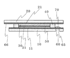
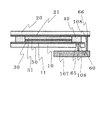
まず初めに図1を用いて、本発明の太陽電池の構造を説明する。図1は本発明の色素増感太陽電池の断面構造を示している。
本発明の色素増感太陽電池の基本的な構成部材は、第1基板10、第1薄膜電極11、第2基板20、第2薄膜電極21、半導体層30、色素31、絶縁スペーサ40、電解質層50、補強層70からなっている。
[Example 1]
First, the structure of the solar cell of the present invention will be described with reference to FIG. FIG. 1 shows a cross-sectional structure of the dye-sensitized solar cell of the present invention.
The basic components of the dye-sensitized solar cell of the present invention are the
第1基板10は透明性のフィルム材を用いており、本発明ではPEN(ポリエチレンナフタレート)を用いているが、その他PET(ポリエチレンテレフタレート)、PC(ポリカーボネート)、PI(ポリイミド)、PA(ポリアミド)、PAI(ポリアミドイミド)など、耐熱性の高分子材が利用することが出来る。
The
第1基板10には第1薄膜電極11が形成されているが、こちらは触媒活性を有した金属薄膜が利用される。主に白金を利用するが、その他パラジウム、ロジウム、オスミウム、イリジウムなども利用可能である。また、これらの金属は高価であるため、非常に薄い膜とし、その下に導通をとるために他の金属材料や酸化物半導体層などを介在させても良い。
A first
第2基板20も基本的に第1基板10と同じように透明フィルム材を用いている。そして、フィルムの表面には第2薄膜電極21が形成されている。第2薄膜電極21は、透明性を有したITO(Indium Tin Oxide)、二酸化スズ、酸化亜鉛などの酸化物半導体が用いられる。
The
さらに第2薄膜電極21の上には二酸化チタンの微粒子からなる半導体層30が形成されている。そして半導体層30の表面には色素31が吸着している。半導体層30にはその他、酸化スズ、酸化タングステン、酸化亜鉛、酸化ニオブなども、利用可能である。ま
た、色素31はビピリジン構造を持つルテニウム錯体、ポルフィリン、フタロシアニンなどの金属錯体、あるいはローダミン、メロシアニン、インドリン、クマリンなど有機色素といった、その目的によって数多くの色素群が利用可能である。
Further, a
図1では半導体層30と色素31は膜が重なったように表現されているが、実際には半導体層30は二酸化チタン微粒子により多孔質構造を有しているため、半導体層30にある無数の孔の表面にも色素31は吸着しており、半導体層30と複合化したような構造となっている。
In FIG. 1, the
この2枚の基板は表面に形成されている両電極を対向させた形で、配置されている。そして、半導体層30の周囲には絶縁スペーサ40が設置され、その厚さ分のクリアランスを持って両基板は接合されている。絶縁スペーサ40には、ホットメルト材、熱硬化性樹脂、紫外線硬化性樹脂などの接着性樹脂が利用され、基本的にスペースを保つことの他に上下の基板を接着するのにも役立っている。
The two substrates are arranged in such a manner that both electrodes formed on the surface face each other. An insulating
絶縁スペーサ40により作られた上下の電極の間隙は電解質層50で満たされている。電解質層50には、ヨウ素、ヨウ素化合物、臭素化合物などの電解質成分を、アセトニトリル、エチレンカーボネート、ポリエチレングリコール、メトキシプロピオニトリルなどに溶解したものが用いられる。
The gap between the upper and lower electrodes formed by the insulating
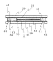
ここまでの構造は従来の色素増感太陽電池とほぼ同じであるが、本発明の色素増感太陽電池では、第1基板10には第1薄膜電極11に至るスルーホール60が形成されている。スルーホール60により第1薄膜電極11の一部は露出するようになっているが、その露出部分は第1接続電極65となっている。
The structure so far is almost the same as that of the conventional dye-sensitized solar cell. However, in the dye-sensitized solar cell of the present invention, the
そして、第1薄膜電極11面上で第1接続電極65の反対面側には補強層70が形成されている。補強層70は熱硬化性あるいは光硬化性などの有機樹脂から構成されており、大きさはスルーホール60の穴径よりも大きく第1接続電極65全体を反対面で覆う形になっている。第1接続電極65は外部と電気的接触をする場合、何らかの手段により電極膜には応力がかかることとなり、薄い電極膜だけでは耐えられない。そこで、補強層70があることで強度的に実用化出来るようになる。
A reinforcing
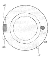
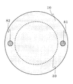
本発明の色素増感太陽電池において、第1基板10と第2基板20はほとんど形状は同じであるが、一部分において異なっている。図2には本発明の色素増感太陽電池を第1基板10側から見た平面図を示している。図2に見られるように、ほぼ円形の第1基板10には、一部切り欠き部63がある。第2基板20は円形をしているため、第1基板10の切り欠き部63から第2基板20の一部が延出している構成となっており、そこにあらわれた部分が第2接続電極66となっている。図面では第2接続電極66の延出部分は第1基板10の切り欠き部であったが、たとえば第1基板10と第2基板20の配置を多少ずらすことで、形成することも出来る。
In the dye-sensitized solar cell of the present invention, the
以上の様な構成を取ることにより、本発明の色素増感太陽電池は、外部への接続をとるための第1接続電極65と第2接続電極66の接続面が同じ方向を向いている。つまり、図1における下方に両電極が向いていることになる。これから、本発明の色素増感太陽電池では、第1基板10に対向させて外部回路を配置することで、直接接続が出来ることになる。
By adopting the above configuration, in the dye-sensitized solar cell of the present invention, the connection surfaces of the
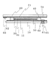
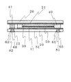
図1に示した構造で、本発明の効果は得られるが、さらに上下基板の接続電極には電極パッドを形成してもよい。その構造は図3に示した。第1接続電極65と第2接続電極66に電気接触するよう、導電性の樹脂からなる第1電極パッド81と第2電極パッド82
が形成されている。導電性樹脂としてはエポキシ系樹脂、アクリル系樹脂やシリコーン系樹脂にカーボンや銀などの導電粒子が混練されているものを用いる。電極パッドがあることで、外部との接続時に薄膜電極に直接接触することがないので、膜の損傷などの危険性がなく、信頼性がさらに高まるものである。
Although the effects of the present invention can be obtained with the structure shown in FIG. 1, electrode pads may be formed on the connection electrodes of the upper and lower substrates. The structure is shown in FIG. A
Is formed. As the conductive resin, an epoxy resin, an acrylic resin, or a silicone resin in which conductive particles such as carbon and silver are kneaded is used. The presence of the electrode pad does not directly contact the thin film electrode when connected to the outside, so there is no risk of film damage and the reliability is further increased.
続いて簡単に本発明の色素増感太陽電池の製造方法を述べる。まず、フィルム状の第1基板10を用意し、スパッタリング法を用いて白金薄膜を形成し第1薄膜電極11とする。この時下地層としてチタン膜を形成しても良い。第1薄膜電極11の上には、その一部に補強層70を設けておく。補強層70は後に太陽電池の接続電極としたい部分に形成するが、エポキシ樹脂をディスペンスあるいは印刷することで塗布しておき、熱や紫外線によって硬化させる。また図示はしていないが、第1基板10には後に電解液を注入するための微小な注入孔を形成しておく。
Next, a method for producing the dye-sensitized solar cell of the present invention will be briefly described. First, a film-like
同じくフィルム状の第2基板20を用意し、やはりスパッタリング法を用いてITO薄膜を形成し、第2薄膜電極21とする。つづいて、二酸化チタンの微粒子をポリエチレングリコール、アルコール、アセトンなどの有機溶媒や水に分散させたペーストを用意し、スキージ法を用いて第2薄膜電極21上に所望の形状で印刷する。ペーストは室温で溶媒をある程度蒸発させた後、電気炉中で焼成して半導体層30とする。この時、二酸化チタンの粒子同士は結合をし、全体の抵抗を下げることとなる。
Similarly, a film-like
さらに色素31を有機溶媒で溶かした色素溶液を用意し、その中に先の第2基板20を浸漬し、半導体層30である二酸化チタン粒子表面に色素31を吸着させる。液から出した後加熱あるいは自然乾燥させることで、色素31付きの基板が出来上がる。
Further, a dye solution in which the
ホットメルト型の接着剤を所望の形状に加工しておき、第2基板20に形成した半導体層30の外周に配置する。第2基板20に対向して先に用意した第1基板10を合わせ、加圧をしながら加熱をする。ホットメルト材は融解することにより上下の基板に親和し、常温に戻すと再度固化し絶縁スペーサ40となり貼り合わせが完了する。
A hot-melt type adhesive is processed into a desired shape and disposed on the outer periphery of the
つづいて、第1基板10の下面よりレーザー光線を照射し、第1基板10の一部を溶解除去しスルーホール60を形成する。スルーホール60は先に形成しておいた補強層70の位置に形成するが、補強層70の面積よりも小さい方がよい。これにより、露出した第1薄膜電極11部分が第1接続電極65となる。
Subsequently, a laser beam is irradiated from the lower surface of the
また、必要に応じて、第1接続電極65と第2接続電極66にはディスペンス法や印刷法を用いて第1電極パッド81と第2電極パッド82を形成する。電極パッドとなる導電性樹脂は原液を所定の場所に配置した後、加熱や紫外線照射により硬化させることで出来上がる。
If necessary, the
最後に、予め形成しておいた第1基板10の注入孔よりシリンジなどを利用して電解液を内部のスペースに注入し電解質層50を形成する。注入孔はホットメルト剤を乗せ、再加熱することで封止する。以上の工程を経ることで、本発明の色素増感太陽電池は完成する。
Finally, the
以上の説明において、スルーホール60の形成は基板を貼り合わせた後に行っていたが、第1基板10に補強層70を形成した後に引き続き行うこともできる。また、第1電極パッド81の形成もこれに引き続いて行える。第2電極パッド82も第2薄膜電極21が形成した後なら、いつ行ってもかまわない。また、スルーホール60は、図面上では第1基板10の内部に形成しているため、文字通り穴の形状をしているが、外周部に形成しても良い。この場合、穴形状ではなく切り欠き部のようになるが、その上に絶縁スペーサ4
0があれば必要な機能は果たすことができる。
〔実施例2〕
In the above description, the formation of the through
If there is 0, the necessary function can be performed.
[Example 2]
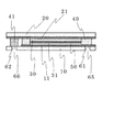
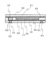
つづいて本発明の色素増感太陽電池における第2の構造を図4に示した。第1基板10、第1薄膜電極11、第2基板20、第2薄膜電極21、半導体層30、色素31、電解質層50、絶縁スペーサ40からなる構成は図1に示した太陽電池と同じであり、第1基板10から延出した第2基板20の部分に第2接続電極66があることも同じである。
Next, the second structure of the dye-sensitized solar cell of the present invention is shown in FIG. The configuration including the
ここで、第2の色素増感太陽電池では、スルーホール60が絶縁スペーサ40の下面に形成されており、つまり絶縁スペーサ40が先に述べた補強層70を兼ねた構造となっている。スルーホール60の大きさは当然ながら、絶縁スペーサ40の幅よりも小さくなっているが、絶縁スペーサ40幅が小さい場合には、スルーホール60を空ける場所に相当する絶縁スペーサ40部分の幅を広くしても良い。この様にして、絶縁スペーサ40の下面に第1接続電極65が形成されるとともに、絶縁スペーサ40で補強されているため、強度的に実用可能な電極となる。
Here, in the second dye-sensitized solar cell, the through
以上の第2の色素増感太陽電池では、絶縁スペーサ40が補強層70を兼ねることにより、製造工程が簡略化できるとともに、絶縁スペーサ40を外周近くまで配置することが可能となることから、発電領域を広範囲に広げることが可能となる。
〔実施例3〕
In the second dye-sensitized solar cell described above, since the insulating
Example 3
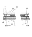
続いて本発明の色素増感太陽電池における第3の構造について、図5を用いて説明する。図5は本発明の色素増感太陽電池の断面構造を示している。 Next, a third structure in the dye-sensitized solar cell of the present invention will be described with reference to FIG. FIG. 5 shows a cross-sectional structure of the dye-sensitized solar cell of the present invention.
第3の実施例における色素増感太陽電池の基本的な構成部材は、透明性のフィルム材からなる第1基板10および第2基板20、金属膜からなる第1薄膜電極11、金属酸化物透明電極である第2薄膜電極21、主に二酸化チタン微粒子からなる半導体層30、色素31、二つの基板を接合する機能を持つ絶縁スペーサ40、電解質層50からなっており、この基本的構成は第2の実施例と同じである。そしてさらに本実施例では導電スペーサ41を設けている。
The basic components of the dye-sensitized solar cell in the third embodiment are the
本実施例における色素増感太陽電池では、絶縁スペーサ40の外周部分に上下の基板に接する導電スペーサ41が設けられている。導電スペーサ41は合成樹脂やゴム系材料にカーボンや銀などの導電粒子が混練されて、固体として導通を有するものである。ただし、第1薄膜電極11は導電スペーサ41に接触しないよう、導電スペーサ41のある部分には形成されていない。
In the dye-sensitized solar cell in the present embodiment,
そして、導電スペーサ41が第1基板10に接しているところにおいて、第1基板10には第2スルーホール62が形成されている。第2スルーホール62は導電スペーサ41まで達するよう形成されていることから、第2スルーホール62の底面には導電スペーサ41が露出しており、第2接続電極66となっている。導電スペーサ41は第2薄膜電極21に電気接触していることから、第2接続電極66では第2薄膜電極21と導通をとることができる。
A second through
また第1基板10の別の場所では第1薄膜電極11に至る第1スルーホール61が形成されている。第1スルーホール61により第1薄膜電極11の一部は露出するようになっているが、その露出部分は第1接続電極65となっている。ただし第1スルーホール61は第1接続電極65の強度を維持するために、絶縁スペーサ40が設けられている部分に形成するのが望ましい。この第1スルーホール61は、基本的に先の実施例に述べてきた、スルーホール60と同じである。
Further, a first through
以上の様な構成を取ることにより、本発明の色素増感太陽電池は、外部への接続をとるための第1接続電極65と第2接続電極66の接続面が同じ面内に存在するようになる。これから、本発明の色素増感太陽電池では、第1基板10に対向させて外部回路を配置するばあい、非常に簡単に直接接続が出来ることになる。
By adopting the above configuration, in the dye-sensitized solar cell of the present invention, the connection surfaces of the
また、図6に示しているように、導電スペーサ41と第1基板10との間には、補助電極12を設けることもできる。補助電極12は第1薄膜電極11と同じ面内で第1基板10の表面に形成されている。補助電極12は金属薄膜からなっているが、基本的に第1薄膜電極11と同じ材料である。補助電極12は金属膜であることから、導電スペーサ41から直接外部接触を取るより、接触抵抗を下げることが可能である。
In addition, as illustrated in FIG. 6, the
さらに図5あるいは図6に示した構造で、本発明の効果は得られるが、さらに上下基板の接続電極には電極パッドを形成してもよい。その構造は図7に示した。第1接続電極65と第2接続電極66に電気接触するよう、導電性の樹脂からなる第1電極パッド81と第2電極パッド82が形成されている。導電性樹脂としてはエポキシ系樹脂、アクリル系樹脂やシリコーン系樹脂にカーボンや銀などの導電粒子が混練されているものを用いる。電極パッドがあることで、外部との接続時に薄膜電極に直接接触することがないので、膜の損傷などの危険性がなく、信頼性が高まる。また第1基板10の表面より突出させることができるため、外部からの接触が容易になる。
In addition, although the effects of the present invention can be obtained with the structure shown in FIG. 5 or FIG. 6, electrode pads may be formed on the connection electrodes of the upper and lower substrates. The structure is shown in FIG. A
また、図8に示したように、導電スペーサ41を絶縁スペーサ40の外周に配置するだけでなく、内部に入り込ませても良い。この構造を平面的に示したのが図9である。両者の図から明らかなように、このような構造をとることで、絶縁スペーサ40を最外周まで配置することができるようになる。これにより、従来のように基板の外周にて基板がフリーの状態になることがなく、また第1薄膜電極11と第2薄膜電極21の膜面がまったく露出していないことから、耐湿性などの信頼性を向上させることができる。さらに、図には示していないが、基板の側面にも絶縁性接着剤などで、封止をするとさらに効果的である。
Further, as shown in FIG. 8, the
続いて第3の実施例の色素増感太陽電池の製造方法を述べる。まず、フィルム状の第1基板10を用意し、スパッタリング法を用いて白金薄膜を形成し第1薄膜電極11とする。基板との密着を取るため、あるいは膜抵抗を下げるために下地層としてチタン、ニッケル、クロム、アルミ膜などを形成しても良い。この第1薄膜電極11を形成する際、導電スペーサ41と接触する部分には、薄膜は形成しない。あるいは第1薄膜電極11となる部分とは電気的に分離させて、補助電極12を第1薄膜電極11と同じ材料で同時に形成する。
Then, the manufacturing method of the dye-sensitized solar cell of the 3rd Example is described. First, a film-like
パターン化された第1薄膜電極11および補助電極12の形成は、形成したい薄膜の形状にあらかじめ加工された金属板マスクを利用し、成膜する際にパターン化を行うことで可能である。あるいは第1基板10のほぼ全面に薄膜を形成し、フォトリソグラフィーを利用したエッチング法によりパターン形成することも出来る。また、図示はしていないが、第1基板10には後に電解液を注入するための微小な注入孔を形成しておく。
The patterned first
同じくフィルム状の第2基板20を用意し、やはりスパッタリング法を用いてITO薄膜を形成し、第2薄膜電極21とする。つづいて、二酸化チタンの微粒子をポリエチレングリコール、アルコール、アセトンなどの有機溶媒や水に分散させたペーストを用意し、スキージ法を用いて第2薄膜電極21上に所望の形状で印刷する。ペーストは室温で溶媒をある程度蒸発させた後、電気炉中で焼成して半導体層30とする。この時、二酸化チタンの粒子同士は結合をし、全体の抵抗を下げることとなる。
Similarly, a film-like
さらに色素31を有機溶媒で溶かした色素溶液を用意し、その中に先の第2基板20を浸漬し、半導体層30である二酸化チタン粒子表面に色素31を吸着させる。液から出した後加熱あるいは自然乾燥させることで、色素31付きの基板が出来上がる。
Further, a dye solution in which the
ホットメルト型の接着剤を所望の形状に加工しておき、第2基板20に形成した半導体層30の外周に配置する。また同時に、電気伝導性のホットメルト型接着剤も第2接続電極66を形成したい場所に配置する。第2基板20に対向して先に用意した第1基板10を合わせ、加圧をしながら加熱をする。ホットメルト材は融解することにより上下の基板に親和し、常温に戻すと再度固化し絶縁スペーサ40と導電スペーサ41となり、貼り合わせが完了する。
A hot-melt type adhesive is processed into a desired shape and disposed on the outer periphery of the
また、貼り合わせに関しては、絶縁スペーサ40の材料として、熱硬化性や光硬化性の接着剤を用意して、半導体層30の外周に配置しても良い。そして、導電スペーサ41の材料としても、導電粒子が混練された熱硬化性や光硬化性の接着剤を使うことも可能である。これらは、印刷あるいはディスペンスなどの工程により第1基板10あるいは第2基板20に接着剤を配置しておき、両基板を合わせた後に加熱あるいは光照射することで硬化させて固定する。
For bonding, a thermosetting or photocurable adhesive may be prepared as the material of the insulating
つづいて、第1基板10の下面よりレーザー光線を照射し、第1基板10の一部を溶解除去し第1スルーホール61を形成する。第1スルーホール61は先に形成しておいた絶縁スペーサ40の位置に形成するが、絶縁スペーサ40の幅よりも小さい方がよい。これにより、露出した第1薄膜電極11部分が第1接続電極65となる。
Subsequently, a laser beam is irradiated from the lower surface of the
同様にレーザー照射により、第2スルーホール62を形成する。第2スルーホール62は導電スペーサ41のある部分に形成するが、導電スペーサ41の幅より小さいほうが望ましい。そして、第2スルーホール62は導電スペーサ41の面あるいは補助電極12の面が露出するまで加工されるが、この露出面が第2接続電極66となる。ここで、第1スルーホール61と第2スルーホール62の形成順はどちらが先でもかまわない。
Similarly, the second through
さらに必要に応じて、第1接続電極65と第2接続電極66にはディスペンス法や印刷法を用いて第1電極パッド81と第2電極パッド82を形成する。電極パッドとなる導電性樹脂は原液を所定の場所に配置した後、加熱や紫外線照射により硬化させることで出来上がる。
Further, if necessary, the
最後に、予め形成しておいた第1基板10の注入孔よりシリンジなどを利用して電解液を内部のスペースに注入し電解質層50を形成する。その後注入孔にはホットメルト剤を乗せ、再加熱することで封止する。以上の工程を経ることで、本発明の色素増感太陽電池は完成する。
Finally, the
以上の説明において出てきた第1スルーホール61と第2スルーホール62は、図面上では第1基板10の内部に形成しているため、文字通り穴の形状をしているが、外周部に形成しても良い。この場合、穴形状ではなく切り欠き部のようになるが、その上に絶縁スペーサ40や導電スペーサ41があれば必要な機能は果たすことができる。また、第1接続電極65と第2接続電極66を隣接させて作る場合は、第1スルーホール61と第2スルーホール62をつなげて一つにすることもできる。
Since the first through
以上それぞれの実施例では、第1基板10にスルーホール60あるいは第1スルーホール、第2スルーホールを形成することとしている。しかしながら、スルーホールは、第2基板20に形成することも可能である。この場合、外部との電気的接触は第2基板側から
行うこととなる。ただし、第2スルーホールを第2基板20に設ける場合は、第1薄膜電極11をパターン化する代わりに、第2薄膜電極21をパターン化するようになる。
In each of the embodiments described above, the through
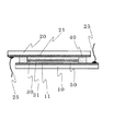
引き続いて、本発明の色素増感太陽電池を腕時計用の発電セルとして利用する場合の構成について説明する。図10には、本発明の色素増感太陽電池を装着した腕時計の断面図を示している。 Subsequently, a configuration when the dye-sensitized solar cell of the present invention is used as a power generation cell for a wristwatch will be described. FIG. 10 shows a cross-sectional view of a wristwatch equipped with the dye-sensitized solar cell of the present invention.
図10ではアナログ式の腕時計を示しており、ケース101、風防ガラス102、裏蓋103で形成された空間に、表示板104、色素増感太陽電池105、ムーブメント106、回路基板107を搭載している。回路基板107は基本的にムーブメント106と一体化しており、ムーブメント106には歯車など機械的な部品、モーター、振動子、二次電池なども含まれている。
FIG. 10 shows an analog wristwatch, in which a
外部光は透明な風防ガラス102を通過し、表示板104に達するが、表示板104は半透明性を有しているため、光の一部はその下部まで達する。表示板104のすぐ下部に色素増感太陽電池105が配置されていることから、色素増感太陽電池105は到達した光で発電することができる。光は風防ガラス102を通して入射するため、色素増感太陽電池105は上側、つまりは風防ガラス102側に透明性を有した基板である、第2基板20が向けられるように配置される。
External light passes through the
色素増感太陽電池105で発電したエネルギーは回路側に供給されるが、そのための回路基板107は色素増感太陽電池105のすぐ下に来るように配置される。本発明の色素増感太陽電池105は図1で説明したように、その第1接続電極65と第2接続電極66が両者とも下側を向いているため、回路基板107とはすぐ近くで対向できる。回路基板107にはあらかじめ導電端子108を備えておくことにより、導電端子108が第1接続電極65と第2接続電極66に直接触ることができ、それぞれは腕時計内部に実装するだけで電気的な接続が取れるようになる。
The energy generated by the dye-sensitized
導電端子108による詳しい接続の様子は図11に示した。図11では、色素増感太陽電池には図4に示したような、絶縁スペーサ40が補強層となっているものを利用しており、第1接続電極65と第2接続電極66がすぐ近くに来るように配置されている。図11より明らかなように、本発明の色素増感太陽電池では、太陽電池の接続電極と外部回路が導電端子108により、簡単に接続できることが分かる。そして、導電端子108は接触を確実にするよう、コイルバネ、板バネ、伸縮性の金属筒の中にバネの入ったバネ棒など、弾性部材を利用するのが良い。
A detailed connection state by the
また実施例3における色素増感太陽電池を用いたときの、導電端子108による詳しい接続の様子は図12に示した。図から明らかなように、第2接続電極66も第1基板10に設けることで、長さの同じ導電端子108を利用でき、接続位置あわせなどがさらに簡単になる。
FIG. 12 shows a detailed connection state by the
そして色素増感太陽電池105から回路基板107に送られた電気エネルギーは、二次電池に蓄えられ、この二次電池のエネルギーを利用して腕時計は継続的に駆動することができるようになる。
The electrical energy sent from the dye-sensitized
なお、本発明の色素増感太陽電池を備えた腕時計では、表示板104の下に色素増感太陽電池105を設置した。しかし、用いる色素増感太陽電池105そのものに文字などを印刷することで、表示板104としての機能を兼ねさせることは可能であり、その場合別の材料で表示板104を供える必要はない。
In the wristwatch provided with the dye-sensitized solar cell of the present invention, the dye-sensitized
10 第1基板
11 第1薄膜電極
12 補助電極
20 第2基板
21 第2薄膜電極
25 リード線
30 半導体層
31 色素
40 絶縁スペーサ
41 導電スペーサ
50 電解質層
60 スルーホール
61 第1スルーホール
62 第2スルーホール
63 切り欠き部
65 第1接続電極
66 第2接続電極
70 補強層
81 第1電極パッド
82 第2電極パッド
101 ケース
102 風防ガラス
103 裏蓋
104 表示板
105 色素増感太陽電池
106 ムーブメント
107 回路基板
108 導電端子
10
Claims (11)
Priority Applications (1)
| Application Number | Priority Date | Filing Date | Title |
|---|---|---|---|
| JP2009054335A JP2010211971A (en) | 2009-03-09 | 2009-03-09 | Dye-sensitized solar cell and wrist watch equipped with the same |
Applications Claiming Priority (1)
| Application Number | Priority Date | Filing Date | Title |
|---|---|---|---|
| JP2009054335A JP2010211971A (en) | 2009-03-09 | 2009-03-09 | Dye-sensitized solar cell and wrist watch equipped with the same |
Publications (1)
| Publication Number | Publication Date |
|---|---|
| JP2010211971A true JP2010211971A (en) | 2010-09-24 |
Family
ID=42971933
Family Applications (1)
| Application Number | Title | Priority Date | Filing Date |
|---|---|---|---|
| JP2009054335A Pending JP2010211971A (en) | 2009-03-09 | 2009-03-09 | Dye-sensitized solar cell and wrist watch equipped with the same |
Country Status (1)
| Country | Link |
|---|---|
| JP (1) | JP2010211971A (en) |
Cited By (6)
| Publication number | Priority date | Publication date | Assignee | Title |
|---|---|---|---|---|
| CN102544377A (en) * | 2012-02-24 | 2012-07-04 | 日月光半导体制造股份有限公司 | Semiconductor structure with photocell and manufacturing method therefor |
| CN103035408A (en) * | 2011-09-30 | 2013-04-10 | 造能科技有限公司 | Solar cell encapsulation structure and circuit design |
| JP2013077459A (en) * | 2011-09-30 | 2013-04-25 | Taiyo Yuden Co Ltd | Solar battery cell |
| WO2015125609A1 (en) * | 2014-02-19 | 2015-08-27 | 株式会社村田製作所 | Light power generation module |
| CN108713234A (en) * | 2016-04-27 | 2018-10-26 | 积水化学工业株式会社 | The construction method of solar cell module and solar cell module |
| JP2020167300A (en) * | 2019-03-29 | 2020-10-08 | 太陽誘電株式会社 | Dye-sensitized solar battery |
Citations (11)
| Publication number | Priority date | Publication date | Assignee | Title |
|---|---|---|---|---|
| JP2005235715A (en) * | 2004-02-23 | 2005-09-02 | Ngk Spark Plug Co Ltd | Dye-sensitized solar cell and solar cell unit panel using it |
| JP2005346934A (en) * | 2004-05-31 | 2005-12-15 | Casio Comput Co Ltd | Dye-sensitized solar cell, ornament device, electronic equipment, and manufacturing method of dye-sensitized solar cell |
| WO2007023881A1 (en) * | 2005-08-26 | 2007-03-01 | Kansai Paint Co., Ltd. | Method for forming electrode pattern, method for connecting electrode patterns, method for forming dye sensitized semiconductor electrode and photoelectric cell module |
| WO2007026927A1 (en) * | 2005-09-02 | 2007-03-08 | Kyocera Corporation | Photo-electric conversion device, its fabrication method, and photovoltaic generation device |
| JP2007059324A (en) * | 2005-08-26 | 2007-03-08 | Kansai Paint Co Ltd | Forming method of dye-sensitized semiconductor electrode and photoelectric cell module |
| JP2007066874A (en) * | 2005-08-02 | 2007-03-15 | Ngk Spark Plug Co Ltd | Dye-sensitized solar cell |
| JP2007066875A (en) * | 2005-08-02 | 2007-03-15 | Ngk Spark Plug Co Ltd | Dye-sensitized solar cell |
| WO2007043533A1 (en) * | 2005-10-11 | 2007-04-19 | Kyocera Corporation | Photoelectric transducer, process for producing the same, and photovoltaic apparatus |
| JP2007280761A (en) * | 2006-04-06 | 2007-10-25 | Kyocera Corp | Photoelectric conversion device, its manufacturing method, and photovoltaic power generation device |
| JP2008021600A (en) * | 2006-07-14 | 2008-01-31 | Meidensha Corp | Die-sensitized solar cell and its manufacturing method |
| JP2008192376A (en) * | 2007-02-01 | 2008-08-21 | Ngk Spark Plug Co Ltd | Solar cell and dye-sensitized solar cell |
-
2009
- 2009-03-09 JP JP2009054335A patent/JP2010211971A/en active Pending
Patent Citations (11)
| Publication number | Priority date | Publication date | Assignee | Title |
|---|---|---|---|---|
| JP2005235715A (en) * | 2004-02-23 | 2005-09-02 | Ngk Spark Plug Co Ltd | Dye-sensitized solar cell and solar cell unit panel using it |
| JP2005346934A (en) * | 2004-05-31 | 2005-12-15 | Casio Comput Co Ltd | Dye-sensitized solar cell, ornament device, electronic equipment, and manufacturing method of dye-sensitized solar cell |
| JP2007066874A (en) * | 2005-08-02 | 2007-03-15 | Ngk Spark Plug Co Ltd | Dye-sensitized solar cell |
| JP2007066875A (en) * | 2005-08-02 | 2007-03-15 | Ngk Spark Plug Co Ltd | Dye-sensitized solar cell |
| WO2007023881A1 (en) * | 2005-08-26 | 2007-03-01 | Kansai Paint Co., Ltd. | Method for forming electrode pattern, method for connecting electrode patterns, method for forming dye sensitized semiconductor electrode and photoelectric cell module |
| JP2007059324A (en) * | 2005-08-26 | 2007-03-08 | Kansai Paint Co Ltd | Forming method of dye-sensitized semiconductor electrode and photoelectric cell module |
| WO2007026927A1 (en) * | 2005-09-02 | 2007-03-08 | Kyocera Corporation | Photo-electric conversion device, its fabrication method, and photovoltaic generation device |
| WO2007043533A1 (en) * | 2005-10-11 | 2007-04-19 | Kyocera Corporation | Photoelectric transducer, process for producing the same, and photovoltaic apparatus |
| JP2007280761A (en) * | 2006-04-06 | 2007-10-25 | Kyocera Corp | Photoelectric conversion device, its manufacturing method, and photovoltaic power generation device |
| JP2008021600A (en) * | 2006-07-14 | 2008-01-31 | Meidensha Corp | Die-sensitized solar cell and its manufacturing method |
| JP2008192376A (en) * | 2007-02-01 | 2008-08-21 | Ngk Spark Plug Co Ltd | Solar cell and dye-sensitized solar cell |
Cited By (9)
| Publication number | Priority date | Publication date | Assignee | Title |
|---|---|---|---|---|
| CN103035408A (en) * | 2011-09-30 | 2013-04-10 | 造能科技有限公司 | Solar cell encapsulation structure and circuit design |
| JP2013077459A (en) * | 2011-09-30 | 2013-04-25 | Taiyo Yuden Co Ltd | Solar battery cell |
| US8772631B2 (en) | 2011-09-30 | 2014-07-08 | Taiyo Yuden Co., Ltd. | Solar cell |
| CN102544377A (en) * | 2012-02-24 | 2012-07-04 | 日月光半导体制造股份有限公司 | Semiconductor structure with photocell and manufacturing method therefor |
| WO2015125609A1 (en) * | 2014-02-19 | 2015-08-27 | 株式会社村田製作所 | Light power generation module |
| CN108713234A (en) * | 2016-04-27 | 2018-10-26 | 积水化学工业株式会社 | The construction method of solar cell module and solar cell module |
| JP2020167300A (en) * | 2019-03-29 | 2020-10-08 | 太陽誘電株式会社 | Dye-sensitized solar battery |
| WO2020203443A1 (en) * | 2019-03-29 | 2020-10-08 | 太陽誘電株式会社 | Dye-sensitized solar cell |
| JP7369538B2 (en) | 2019-03-29 | 2023-10-26 | 太陽誘電株式会社 | dye-sensitized solar cells |
Similar Documents
| Publication | Publication Date | Title |
|---|---|---|
| JP5080018B2 (en) | Dye-sensitized solar cell | |
| JP2010211971A (en) | Dye-sensitized solar cell and wrist watch equipped with the same | |
| CN109478469B (en) | Solar cell module | |
| WO2012118050A1 (en) | Dye-sensitized solar cell and process of manufacturing same, and dye-sensitized solar cell module and process of manufacturing same | |
| JP2006244954A (en) | Wiring connection structure of dye-sensitized solar battery cell and dye-sensitized solar cell module | |
| KR20120113223A (en) | Dye-sensitized solar cell and method for manufacturing the same | |
| JP2007066875A (en) | Dye-sensitized solar cell | |
| TW201818576A (en) | Solar cell module | |
| JP5032051B2 (en) | Dye-sensitized solar cell | |
| JP5230961B2 (en) | Dye-sensitized solar cell | |
| JPWO2018047550A1 (en) | Solar cell module | |
| KR20130023027A (en) | Photoelectric conversion module and the manufacturing method for the same | |
| JP5095226B2 (en) | Dye-sensitized solar cell and method for producing the same | |
| JP2008147037A (en) | Wet type solar cell and its manufacturing method | |
| JP2008258028A (en) | Dye-sensitized solar cell | |
| JP2007317454A (en) | Dye-sensitized solar cell | |
| JP2009199782A (en) | Dye-sensitized solar cell and manufacturing method therefor | |
| JP5095237B2 (en) | Dye-sensitized solar cell and method for producing the same | |
| US20120085393A1 (en) | Solar cell module and method of manufacturing the same | |
| JP4606754B2 (en) | Photoelectric conversion element | |
| JP5032060B2 (en) | Dye-sensitized solar cell | |
| JP5668040B2 (en) | Dye-sensitized solar cell | |
| JP5400737B2 (en) | Solar cell module and method for manufacturing solar cell module | |
| JP2013125633A (en) | Solar battery module | |
| JP2009016174A (en) | Photoelectric conversion element |
Legal Events
| Date | Code | Title | Description |
|---|---|---|---|
| A621 | Written request for application examination |
Free format text: JAPANESE INTERMEDIATE CODE: A621 Effective date: 20111202 |
|
| RD07 | Notification of extinguishment of power of attorney |
Free format text: JAPANESE INTERMEDIATE CODE: A7427 Effective date: 20130523 |
|
| A521 | Written amendment |
Free format text: JAPANESE INTERMEDIATE CODE: A821 Effective date: 20130523 |
|
| A131 | Notification of reasons for refusal |
Free format text: JAPANESE INTERMEDIATE CODE: A131 Effective date: 20130723 |
|
| A02 | Decision of refusal |
Free format text: JAPANESE INTERMEDIATE CODE: A02 Effective date: 20131119 |