JP2010098235A - Non-volatile semiconductor storage device and method of manufacturing the same - Google Patents
Non-volatile semiconductor storage device and method of manufacturing the same Download PDFInfo
- Publication number
- JP2010098235A JP2010098235A JP2008269804A JP2008269804A JP2010098235A JP 2010098235 A JP2010098235 A JP 2010098235A JP 2008269804 A JP2008269804 A JP 2008269804A JP 2008269804 A JP2008269804 A JP 2008269804A JP 2010098235 A JP2010098235 A JP 2010098235A
- Authority
- JP
- Japan
- Prior art keywords
- layer
- memory device
- semiconductor memory
- nonvolatile semiconductor
- protruding
- Prior art date
- Legal status (The legal status is an assumption and is not a legal conclusion. Google has not performed a legal analysis and makes no representation as to the accuracy of the status listed.)
- Granted
Links
Images


Classifications
-
- H—ELECTRICITY
- H10—SEMICONDUCTOR DEVICES; ELECTRIC SOLID-STATE DEVICES NOT OTHERWISE PROVIDED FOR
- H10B—ELECTRONIC MEMORY DEVICES
- H10B43/00—EEPROM devices comprising charge-trapping gate insulators
- H10B43/20—EEPROM devices comprising charge-trapping gate insulators characterised by three-dimensional arrangements, e.g. with cells on different height levels
-
- H—ELECTRICITY
- H10—SEMICONDUCTOR DEVICES; ELECTRIC SOLID-STATE DEVICES NOT OTHERWISE PROVIDED FOR
- H10B—ELECTRONIC MEMORY DEVICES
- H10B43/00—EEPROM devices comprising charge-trapping gate insulators
- H10B43/10—EEPROM devices comprising charge-trapping gate insulators characterised by the top-view layout
-
- H—ELECTRICITY
- H10—SEMICONDUCTOR DEVICES; ELECTRIC SOLID-STATE DEVICES NOT OTHERWISE PROVIDED FOR
- H10B—ELECTRONIC MEMORY DEVICES
- H10B43/00—EEPROM devices comprising charge-trapping gate insulators
- H10B43/20—EEPROM devices comprising charge-trapping gate insulators characterised by three-dimensional arrangements, e.g. with cells on different height levels
- H10B43/23—EEPROM devices comprising charge-trapping gate insulators characterised by three-dimensional arrangements, e.g. with cells on different height levels with source and drain on different levels, e.g. with sloping channels
- H10B43/27—EEPROM devices comprising charge-trapping gate insulators characterised by three-dimensional arrangements, e.g. with cells on different height levels with source and drain on different levels, e.g. with sloping channels the channels comprising vertical portions, e.g. U-shaped channels
Landscapes
- Semiconductor Memories (AREA)
- Non-Volatile Memory (AREA)
Abstract
Description
本発明は、電気的にデータの書き換えが可能な不揮発性半導体記憶装置、及びその製造方法に関する。 The present invention relates to a nonvolatile semiconductor memory device capable of electrically rewriting data and a method for manufacturing the same.
従来、シリコン基板上の2次元平面内に素子を集積して、LSIが形成されてきた。メモリの記憶容量を増加させるには、一素子の寸法を小さくする(微細化する)ことにより主に達せられてきたが、近年その微細化もコスト的、技術的に困難なものになってきた。微細化のためにはフォトリソグラフィの技術向上が必要であるが、例えば、現在のArF液浸露光技術では40nm付近のルールが解像限界となっており、更なる微細化のためにはEUV露光機の導入が必要である。しかし、EUV露光機はコスト高であり、コストを考えた場合には現実的ではない。また、仮に微細化が達成されたとしても、駆動電圧などがスケーリングされない限り、素子間の耐圧など物理的な限界点を迎える事が予想される。つまり、デバイスとしての動作が困難になる可能性が高い。 Conventionally, LSIs have been formed by integrating elements in a two-dimensional plane on a silicon substrate. In order to increase the storage capacity of the memory, it has mainly been achieved by reducing (miniaturizing) the size of one element, but in recent years, the miniaturization has become difficult in terms of cost and technology. . For miniaturization, photolithography technology needs to be improved. For example, in the current ArF immersion exposure technology, the rule near 40 nm is the resolution limit, and for further miniaturization, EUV exposure is required. It is necessary to introduce a machine. However, the EUV exposure apparatus is expensive, and it is not realistic when considering the cost. Even if miniaturization is achieved, it is expected that physical limits such as breakdown voltage between elements will be reached unless the drive voltage is scaled. That is, there is a high possibility that operation as a device is difficult.
そこで、近年、メモリの集積度を高めるために、メモリセルを3次元的に配置した半導体記憶装置が多数提案されている(特許文献1乃至3参照)。 In recent years, therefore, many semiconductor memory devices in which memory cells are arranged three-dimensionally have been proposed in order to increase the degree of memory integration (see Patent Documents 1 to 3).
メモリセルを3次元的に配置した従来の半導体記憶装置の一つに、円柱型構造のトランジスタを用いた半導体記憶装置がある(特許文献1乃至3)。円柱型構造のトランジスタを用いた半導体記憶装置においては、ゲート電極となる多層に積層された積層導電層(ワード線導電層)、及びピラー状の柱状半導体が層設けられる。柱状半導体層は、トランジスタのチャネル(ボディ)部として機能する。柱状半導体層の周りには、電荷を蓄積可能なメモリゲート絶縁層が設けられる。これら積層導電層、柱状半導体、メモリゲート絶縁層を含む構成は、メモリストリングスと呼ばれる。 As one of conventional semiconductor memory devices in which memory cells are arranged three-dimensionally, there is a semiconductor memory device using a transistor having a cylindrical structure (Patent Documents 1 to 3). In a semiconductor memory device using a columnar transistor, a stacked conductive layer (word line conductive layer) stacked in multiple layers to be a gate electrode and a pillar-shaped columnar semiconductor are provided. The columnar semiconductor layer functions as a channel (body) portion of the transistor. A memory gate insulating layer capable of storing electric charge is provided around the columnar semiconductor layer. A configuration including these stacked conductive layers, columnar semiconductors, and memory gate insulating layers is called a memory string.
上記メモリストリングスを有する半導体記憶装置において、積層導電層の基板に平行な所定方向の端部は、階段状に形成されている。そして、その積層導電層の階段状の端部上面に、上方から延びるコンタクト層(コンタクトプラグ)が形成されている。コンタクト層は、積層導電層の上層に設けられた導電層と積層導電層とを導通させるための層である。このような構成は、製造時においてクリティカルなリソグラフィー工程を必要としない点でコスト的に優位である。一方、コンタクト層は、階段状の積層導電層に達するように形成されているので、そのコンタクト層の深さは、不均一となる。そこで、不均一深さの孔を一度に確実に開孔するために、階段状の積層導電層端部にはエッチングストッパー材等を堆積することが望ましい。しかしながら、このエッチングストッパー材の膜圧の分、階段状となるステップ幅を広くする必要がある。すなわち、これは、半導体記憶装置全体の占有面積(チップ全体の面積)を更に縮小する際の問題となっていた。
本発明は、占有面積を縮小した不揮発性半導体記憶装置、及びその製造方法を提供する。 The present invention provides a nonvolatile semiconductor memory device having a reduced occupation area and a method for manufacturing the same.
本発明の一態様に係る不揮発性半導体記憶装置は、電気的に書き換え可能であり且つ直列接続された複数のメモリセルを含むメモリストリングスを備える不揮発性半導体記憶装置であって、基板に対して上方に突出して形成された突出層を備え、前記メモリストリングスは、前記基板上に積層された複数の導電層と、当該複数の導電層を貫通するように形成された半導体層と、前記導電層と前記半導体層との間に形成され且つ電荷を蓄積可能に構成された電荷蓄積層とを備え、前記複数の導電層は、前記基板に対して平行に延びる底部と、当該底部の端部にて前記突出層に沿って前記基板に対して上方に延びる側部とを備え、前記基板に平行な第1方向の前記突出層の幅は、積層方向の前記突出層の長さ以下であることを特徴とする。 A nonvolatile semiconductor memory device according to one embodiment of the present invention is a nonvolatile semiconductor memory device including a memory string that includes a plurality of memory cells that are electrically rewritable and connected in series. The memory string includes a plurality of conductive layers stacked on the substrate, a semiconductor layer formed so as to penetrate the plurality of conductive layers, and the conductive layer. A charge storage layer formed between the semiconductor layer and configured to be capable of storing charges, wherein the plurality of conductive layers are formed at a bottom portion extending in parallel to the substrate and at an end of the bottom portion. A side portion extending upward with respect to the substrate along the protruding layer, wherein a width of the protruding layer in a first direction parallel to the substrate is equal to or less than a length of the protruding layer in the stacking direction. Features.
本発明の一態様に係る不揮発性半導体記憶装置の製造方法は、電気的に書き換え可能であり且つ直列接続された複数のメモリセルを含むメモリストリングスを有する不揮発性半導体記憶装置の製造方法であって、基板に平行な第1方向の幅が積層方向の長さ以下であり且つ前記基板に対して上方に突出する突出層を形成する工程と、前記基板上に前記突出層を覆うように複数の導電層を積層する工程と、積層した複数の前記導電層を前記突出層の上面まで平坦化する工程とを備えることを特徴とする。 A method for manufacturing a nonvolatile semiconductor memory device according to one embodiment of the present invention is a method for manufacturing a nonvolatile semiconductor memory device having memory strings including a plurality of memory cells that are electrically rewritable and connected in series. A step of forming a protruding layer having a width in a first direction parallel to the substrate that is equal to or less than a length in the stacking direction and protruding upward with respect to the substrate; and a plurality of layers so as to cover the protruding layer on the substrate A step of laminating a conductive layer; and a step of planarizing the plurality of laminated conductive layers up to an upper surface of the projecting layer.
本発明は、占有面積を縮小した不揮発性半導体記憶装置、及びその製造方法を提供することが可能となる。 The present invention can provide a nonvolatile semiconductor memory device with a reduced occupation area and a method for manufacturing the same.
以下、図面を参照して、本発明に係る不揮発性半導体記憶装置の実施形態について説明する。 Hereinafter, embodiments of a nonvolatile semiconductor memory device according to the present invention will be described with reference to the drawings.
[第1実施形態]
(第1実施形態に係る不揮発性半導体記憶装置100の構成)
図1は、本発明の第1実施形態に係る不揮発性半導体記憶装置100の概略図を示す。図1に示すように、第1実施形態に係る不揮発性半導体記憶装置100は、主として、メモリトランジスタ領域(第1の領域)12、ワード線駆動回路13、ソース側選択ゲート線(SGS)駆動回路14、ドレイン側選択ゲート線(SGD)駆動回路15、センスアンプ16を有する。メモリトランジスタ領域12は、データを記憶するメモリトランジスタを有する。ワード線駆動回路13は、ワード線WLにかける電圧を制御する。ソース側選択ゲート線(SGS)駆動回路14は、ソース側選択ゲート線SGSにかける電圧を制御する。ドレイン側選択ゲート線(SGD)駆動回路15は、ドレイン側選択ゲート線(SGD)にかける電圧を制御する。センスアンプ16は、メモリトランジスタから読み出した電位を増幅する。なお、上記の他、第1実施形態に係る不揮発性半導体記憶装置100は、ビット線BLにかける電圧を制御するビット線駆動回路、ソース線SLにかける電圧を制御するソース線駆動回路を有する(図示略)。
[First Embodiment]
(Configuration of Nonvolatile
FIG. 1 is a schematic view of a nonvolatile
また、図1に示すように、第1実施形態に係る不揮発性半導体記憶装置100において、メモリトランジスタ領域12を構成するメモリトランジスタは、半導体層を複数積層することによって形成されている。また、図1に示すとおり各層のワード線WLの底部は、水平方向において2次元的に広がりを有するように形成されている。各層のワード線WLの底部は、それぞれ同一層からなる板状の平面構造となっている。各層のワード線WLの側部は、上方に延びて、その端部が水平方向に揃うように形成されている。
As shown in FIG. 1, in the nonvolatile
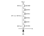
図2は、第1実施形態に係る不揮発性半導体記憶装置100のメモリトランジスタ領域12の一部の概略斜視図である。第1実施形態においては、メモリトランジスタ領域12は、メモリトランジスタMTr1mn〜MTr4mn、ソース側選択トランジスタSSTrmn及びドレイン側選択トランジスタSDTrmnからなるメモリストリングスMSをm×n個(m、nは自然数)を有している。図2においては、m=3、n=4の一例を示している。
FIG. 2 is a schematic perspective view of a part of the memory transistor region 12 of the nonvolatile
各メモリストリングスMSのメモリトランジスタMTr1mn〜MTr4mnのゲートに接続されているワード線WL1〜WL4は、それぞれ同一の導電膜によって形成されており、それぞれ共通である。即ち、各メモリストリングスMSのメモリトランジスタMTr1mnのゲートの全てがワード線WL1に接続されている。また、各メモリストリングスMSのメモリトランジスタMTr2mnのゲートの全てがワード線WL2に接続されている。また、各メモリストリングスMSのメモリトランジスタMTr3mnのゲートの全てがワード線WL3に接続されている。また、各メモリストリングスMSのメモリトランジスタMTr4mnのゲートの全てがワード線WL4に接続されている。第1実施形態に係る不揮発性半導体記憶装置100においては、図1及び図2に示すように、ワード線WL1〜WL4は、それぞれ、半導体基板Baと平行な水平方向において2次元的に広がりを有するように形成されている。また、ワード線WL1〜WL4の底部は、それぞれ、メモリストリングスMSに略垂直に配置されている。ここで、ロウ方向は、垂直方向に直交する方向であり、カラム方向は、垂直方向及びロウ方向に直交する方向である。
The word lines WL1 to WL4 connected to the gates of the memory transistors MTr1mn to MTr4mn of each memory string MS are formed by the same conductive film and are common to each other. That is, all the gates of the memory transistors MTr1mn of each memory string MS are connected to the word line WL1. Further, all the gates of the memory transistors MTr2mn of each memory string MS are connected to the word line WL2. Further, all the gates of the memory transistors MTr3mn of each memory string MS are connected to the word line WL3. Further, all the gates of the memory transistors MTr4mn of each memory string MS are connected to the word line WL4. In the nonvolatile
各メモリストリングスMSは、半導体基板BaのP−well領域Ba1に形成されたn+領域(後述するBa2)の上に柱状の柱状半導体CLmn(図2に示す場合、m=1〜3、n=1〜4)を有している。各柱状半導体CLmnは、半導体基板Baから垂直方向に形成されており、半導体基板Ba及びワード線WL1〜WL4の底部の面上においてマトリクス状になるように配置されている。つまり、メモリストリングスMSも、柱状半導体CLmnに垂直な面内にマトリクス状に配置されている。なお、この柱状半導体CLmnは、円柱状であっても、角柱状であってもよい。また、柱状半導体CLmnとは、段々形状を有する柱状の半導体を含む。 Each memory string MS has a columnar columnar semiconductor CLmn (in the case of FIG. 2, m = 1 to 3, n = 1) on an n + region (Ba2 described later) formed in the P-well region Ba1 of the semiconductor substrate Ba. To 4). Each columnar semiconductor CLmn is formed in the vertical direction from the semiconductor substrate Ba, and is arranged in a matrix on the bottom surface of the semiconductor substrate Ba and the word lines WL1 to WL4. That is, the memory strings MS are also arranged in a matrix in a plane perpendicular to the columnar semiconductor CLmn. The columnar semiconductor CLmn may be cylindrical or prismatic. The columnar semiconductor CLmn includes a columnar semiconductor having a stepped shape.
また、図2に示すように、メモリストリングスMSの上方には、柱状半導体CLmnと絶縁膜(図示せず)を介し接してドレイン側選択トランジスタSDTrmnを構成する矩形板状のドレイン側選択ゲート線SGD(図2に示す場合、SGD1〜SGD4)が設けられている。各ドレイン側選択ゲート線SGDは、互いに絶縁分離され、ワード線WL1〜WL4とは異なり、ロウ方向に延びカラム方向に繰り返し設けられたライン状に形成されている。また、ドレイン側選択ゲート線SGDのカラム方向の中心を貫通して、柱状半導体CLmnが設けられている。 Further, as shown in FIG. 2, a rectangular plate-shaped drain-side selection gate line SGD that forms a drain-side selection transistor SDTrmn in contact with the columnar semiconductor CLmn via an insulating film (not shown) is disposed above the memory string MS. (In the case shown in FIG. 2, SGD1 to SGD4) are provided. Each drain-side selection gate line SGD is insulated and separated from each other, and is formed in a line extending in the row direction and repeatedly provided in the column direction, unlike the word lines WL1 to WL4. A columnar semiconductor CLmn is provided so as to penetrate the center in the column direction of the drain-side selection gate line SGD.
また、図2に示すように、メモリストリングスMSの下方には、柱状半導体CLmnと絶縁膜(図示せず)を介し接してソース側選択トランジスタSSTrmnを構成するソース側選択ゲート線SGSが設けられている。ソース側選択ゲート線SGSは、ワード線WL1〜WL4の底部と同様に水平方向において2次元的に広がりを有するように形成されている。なお、ソース側選択ゲート線SGSは、図2に示すような構造の他、ロウ方向に延び且つカラム方向に繰り返し設けられた短冊状であってもよい。 As shown in FIG. 2, a source side select gate line SGS that constitutes a source side select transistor SSTrmn is provided below the memory strings MS and in contact with the columnar semiconductor CLmn via an insulating film (not shown). Yes. The source side select gate line SGS is formed so as to expand two-dimensionally in the horizontal direction like the bottoms of the word lines WL1 to WL4. In addition to the structure shown in FIG. 2, the source side select gate line SGS may have a strip shape extending in the row direction and repeatedly provided in the column direction.
次に、図2及び図3を参照して、第1実施形態におけるメモリストリングスMSにより構成される回路構成及びその動作を説明する。図3は、第1実施形態における一つのメモリストリングスMSの回路図である。 Next, with reference to FIG. 2 and FIG. 3, a circuit configuration constituted by the memory string MS in the first embodiment and its operation will be described. FIG. 3 is a circuit diagram of one memory string MS in the first embodiment.
図2及び図3に示すように、第1実施形態において、メモリストリングスMSは、4つのメモリトランジスタMTr1mn〜MTr4mn並びにソース側選択トランジスタSSTrm及びドレイン側選択トランジスタSDTrmnを有している。これら4つのメモリトランジスタMTr1mn〜MTr4mn並びにソース側選択トランジスタSSTrmn及びドレイン側選択トランジスタSDTrmnは、それぞれ直列に接続されている(図3参照)。第1実施形態のメモリストリングスMSにおいては、半導体基板Ba上のP−型領域(P−Well領域)Ba1に形成されたn+領域に柱状半導体CLmnが形成されている。 As shown in FIGS. 2 and 3, in the first embodiment, the memory string MS includes four memory transistors MTr1mn to MTr4mn, a source side selection transistor SSTrm, and a drain side selection transistor SDTrmn. The four memory transistors MTr1mn to MTr4mn, the source side select transistor SSTrmn, and the drain side select transistor SDTrmn are connected in series (see FIG. 3). In the memory string MS of the first embodiment, the columnar semiconductor CLmn is formed in the n + region formed in the P− type region (P-well region) Ba1 on the semiconductor substrate Ba.
また、ソース側選択トランジスタSSTrmnのソースにはソース線SL(半導体基板BaのP−well領域Ba1に形成されたn+領域)が接続されている。また、ドレイン側選択トランジスタSDTrmnのドレインにはビット線BLが接続されている。 A source line SL (n + region formed in the P-well region Ba1 of the semiconductor substrate Ba) is connected to the source of the source side select transistor SSTrmn. A bit line BL is connected to the drain of the drain side select transistor SDTrmn.
各メモリトランジスタMTrmnは、柱状半導体CLmn、その柱状半導体CLmnを取り囲むように形成された電荷蓄積層、その電荷蓄積層を取り囲むように形成されたワード線WLを有する。ワード線WLは、メモリトランジスタMTrmnの制御ゲート電極として機能する。 Each memory transistor MTrmn has a columnar semiconductor CLmn, a charge storage layer formed so as to surround the columnar semiconductor CLmn, and a word line WL formed so as to surround the charge storage layer. The word line WL functions as a control gate electrode of the memory transistor MTrmn.
上記構成を有する不揮発性半導体記憶装置100においては、ビット線BL1〜BL3、ドレイン側選択ゲート線SGD、ワード線WL1〜WL4、ソース側選択ゲート線SGS、ソース線SLの電圧は、ビット線駆動回路(図示略)、ドレイン側選択ゲート線駆動回路15、ワード線駆動回路13、ソース側選択ゲート線駆動回路14、ソース線駆動回路(図示略)によって制御される。すなわち、所定のメモリトランジスタMTrmnの電荷蓄積層の電荷を制御することによって、データの読み出し、書き込み、消去を実行する。
In the nonvolatile
(第1実施形態に係る不揮発性半導体記憶装置100の具体的構成)
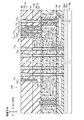
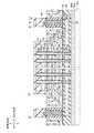
次に、図4を参照して、第1実施形態に係る不揮発性半導体記憶装置100の更に具体的構成を説明する。図4は、第1実施形態に係る不揮発性半導体記憶装置のロウ方向の断面図である。
(Specific Configuration of Nonvolatile
Next, a more specific configuration of the nonvolatile
不揮発性半導体記憶装置100は、半導体基板Ba上に、順次、ソース側選択トランジスタ層20、メモリトランジスタ層30、及びドレイン側選択トランジスタ層40を有する。ソース側選択トランジスタ層20は、ソース側選択トランジスタSSTrmnとして機能する。メモリトランジスタ層30は、メモリトランジスタMTrmnとして機能する。ドレイン側選択トランジスタ層40は、ドレイン側選択トランジスタSDTrmnとして機能する。ソース側選択トランジスタ層20、メモリトランジスタ層30、及びドレイン側選択トランジスタ層40にて、メモリストリングスMSが構成される。
The nonvolatile
ここで、図5は、不揮発性半導体記憶装置100におけるソース側選択トランジスタ層20に含まれる導電層、メモリトランジスタ層30に含まれる導電層、及びドレイン側選択トランジスタ層40に含まれる導電層の形成領域ARを示す上面図である。図5に示すように、形成領域ARは、カラム方向及びロウ方向に所定のピッチを設けて形成されている。形成領域ARは、上方からみてロウ方向に延びる矩形状に形成されている。
Here, FIG. 5 shows the formation of the conductive layer included in the source side
不揮発性半導体記憶装置100は、図4に示すように、半導体基板Ba上にP−型領域(P−Well領域)Ba1を有する。また、不揮発性半導体記憶装置100は、P−型領域Ba1上にn+領域(ソース線領域)Ba2を有する。
As shown in FIG. 4, the nonvolatile
不揮発性半導体記憶装置100は、メモリトランジスタ層30と同層に突出層50を有する。図6は、メモリトランジスタ層30及び突出層50の概略上面図である。突出層50は、図6に示すように、ロウ方向及びカラム方向に所定ピッチを設けて形成されている。突出層50は、上方からみて矩形状であり、半導体基板Baに対して上方に突出して形成されている。突出層50は、上方から示すと、カラム方向に長手を有する矩形状に形成されている。ロウ方向の突出層50の幅は、積層方向の突出層50の長さ以下である(図4参照)。すなわち、アスペクト比は、1以上である。例えば、突出層50の面積が不揮発性半導体記憶装置100に係るチップ全体の面積に占める割合は、1%以下である。
The nonvolatile
突出層50は、柱状に形成された柱状層51、及び柱状層51の側壁に形成された側壁層52を有する。柱状層51は、酸化シリコン(SiO2)にて構成されている。側壁層52は、窒化シリコン(SiN)にて構成されている。
The protruding
ソース側選択トランジスタ層20は、半導体基板Ba上に順次積層された、ソース側第1絶縁層21、ソース側導電層22、ソース側第2絶縁層23、及びソース側分離絶縁層24を有する。
The source side
ソース側第1絶縁層21、ソース側導電層22、ソース側第2絶縁層23、及びソース側分離絶縁層24は、半導体基板Baと平行な水平方向において2次元的に広がりを有するように形成されている。ソース側第1絶縁層21、ソース側導電層22、ソース側第2絶縁層23、及びソース側分離絶縁層24は、メモリトランジスタ領域12内の所定領域(消去単位)毎に分断されている。また、半導体基板Ba上からソース第2絶縁層23の上面に達するまで、層間絶縁層25が設けられている。
The source-side first insulating
ソース側第1絶縁層21、及びソース側第2絶縁層23は、酸化シリコン(SiO2)にて構成されている。ソース側導電層22は、P+型のポリシリコン(p−Si)にて構成されている。ソース側分離絶縁層24は、窒化シリコン(SiN)にて構成されている。層間絶縁層25は、酸化シリコン(SiO2)にて構成されている。
The source side first insulating
また、ソース側分離絶縁層24、ソース側第2絶縁層23、ソース側導電層22、及びソース側第1絶縁層21を貫通するようにソース側ホール26が形成されている。ソース側ホール26に面する側壁には、順次、ソース側ゲート絶縁層27、ソース側柱状半導体層28が設けられている。
A source-
ソース側ゲート絶縁層27は、酸化シリコン(SiO2)にて形成されている。ソース側柱状半導体層28は、ポリシリコン(p−Si)にて形成されている。
The source side
なお、上記ソース側選択トランジスタ20の構成において、ソース側導電層22の構成を換言すると、ソース側導電層22は、ソース側柱状半導体層28と共にソース側ゲート絶縁層27を挟むように形成されている。
In the configuration of the source side
また、ソース側選択トランジスタ層20において、ソース側導電層22が、ソース側選択ゲート線SGSとして機能する。また、ソース側導電層22が、ソース側選択トランジスタSSTrmnの制御ゲートとして機能する。
In the source side
メモリトランジスタ層30は、ソース側分離絶縁層24の上方に設けられた第1〜第4ワード線導電層31a〜31dと、第1〜第4ワード線導電層31a〜31dの間に設けられた第1〜第4ワード線間絶縁層32a〜32dと、第4ワード線間絶縁層32d上に積層されたメモリ分離絶縁層33を有する。
The
第1〜第4ワード線導電層31a〜31dは、図4に示すロウ方向断面にて、上方に開口を向ける「コの字」状(凹型)に形成されている。第1〜第4ワード線導電層31a〜31dは、第1〜第4底部311a〜311d、及び第1〜第4側部312a〜312dを有する。
The first to fourth word line
第1〜第4底部311a〜311dは、半導体基板Baに対して平行に延びるように形成されている。第2底部311bのロウ方向の幅は、第1底部311aのロウ方向の幅よりも短い。第3底部311cのロウ方向の幅は、第2底部311bのロウ方向の幅よりも短い。第4底部311dのロウ方向の幅は、第3底部311cのロウ方向の幅よりも短い。
The first to
第1〜第4側部312a〜312dは、突出層50に沿って半導体基板Baに対して直交上方に延びるように形成されている。したがって、図6に示すようにメモリトランジスタ層30を上面から示すと、第1〜第4側部312a〜312dは、ロウ方向に所定ピッチを設けてストライプ状に形成されている。第1〜第4側部312a〜312dの上面は、水平方向の同一平面内に揃うように形成されている。
The first to
第1〜第4ワード線導電層31a〜31dは、P+型のポリシリコン(p−Si)にて構成されている。第1〜第4ワード線間絶縁層32a〜32dは、酸化シリコン(SiO2)にて構成されている。メモリ分離絶縁層33は、窒化シリコン(SiN)にて構成されている。
The first to fourth word line
また、メモリトランジスタ層30において、メモリ分離絶縁層33、第1〜第4ワード線間絶縁層32a〜32d、及び第1〜第4ワード線導電層31a〜31dを貫通するようにメモリホール34が形成されている。メモリホール34は、ソース側ホール26と整合する位置に設けられている。メモリホール34内の側壁には、順次、メモリゲート絶縁層35、及びメモリ柱状半導体層36が設けられている。
In the
メモリゲート絶縁層35は、図7に示すように構成されている。図7は、図4に示すメモリトランジスタ層30の拡大図である。図7に示すように、メモリゲート絶縁層35は、メモリ柱状半導体層部36の側壁から、順次、トンネル絶縁層35a、電荷を蓄積する電荷蓄積層35b、及びブロック絶縁層35cを有する。
The memory
トンネル絶縁層35a、及びブロック絶縁層35cは、酸化シリコン(SiO2)にて形成されている。電荷蓄積層35bは、窒化シリコン(SiN)にて形成されている。メモリ柱状半導体層36は、ポリシリコン(p−Si)にて構成されている。また、メモリ柱状半導体層36は、その上部をN+型のポリシリコンにて構成されたものであってもよい。
The
なお、上記メモリトランジスタ30において、第1〜第4ワード線導電層31a〜31dの構成を換言すると、第1〜第4ワード線導電層31a〜31dは、メモリ柱状半導体層36と共にトンネル絶縁層35a、電荷蓄積層35b及びブロック絶縁層35cを挟むように形成されている。また、メモリ柱状半導体層36は、ソース側柱状半導体層28の上面、及び後述するドレイン側柱状半導体層47の下面に接するように形成されている。
In other words, in the
また、メモリトランジスタ層30において、第1〜第4ワード線導電層31a〜31dが、ワード線WL1〜WL4として機能する。また、第1〜第4ワード線導電層31a〜31dが、メモリトランジスタMTrmnの制御ゲートとして機能する。
In the
ドレイン側選択トランジスタ層40は、メモリ分離絶縁層33上に順次積層されたドレイン側第1絶縁層41、ドレイン側導電層42、及びドレイン側第2絶縁層43を有する。
The drain side
ドレイン側第1絶縁層41、ドレイン側導電層42、及びドレイン側第2絶縁層43は、メモリ柱状半導体層36の上部に整合する位置に設けられ且つロウ方向に延びカラム方向に繰り返し設けられたライン状に形成されている。また、ドレイン側第1絶縁層41の上面からドレイン側第2絶縁層43の上面まで、層間絶縁層44が形成されている。
The drain-side first insulating
ドレイン側第1絶縁層41及びドレイン側第2絶縁層43は、酸化シリコン(SiO2)にて形成されている。ドレイン側導電層42は、P+型のポリシリコン(p−Si)にて形成されている。層間絶縁層44は、酸化シリコン(SiO2)にて形成されている。
The drain side first insulating
また、ドレイン側選択トランジスタ層40において、ドレイン側第2絶縁層43、ドレイン側導電層42、ドレイン側第1絶縁層41、及びメモリ分離絶縁層33を貫通するようにドレイン側ホール45が形成されている。ドレイン側ホール45は、メモリホール34と整合する位置に設けられている。ドレイン側ホール45に面する側壁には、順次、ドレイン側ゲート絶縁層46、及びドレイン側柱状半導体層47が設けられている。
In the drain side
ドレイン側ゲート絶縁層46は、酸化シリコン(SiO2)にて形成されている。ドレイン側柱状半導体層47は、ポリシリコン(p−Si)にて形成されている。また、ドレイン側柱状半導体層47の上部は、N+型ポリシリコンにて構成されている。
The drain side
なお、上記ドレイン側選択トランジスタ40の構成において、ドレイン側導電層42の構成を換言すると、ドレイン側導電層42は、ドレイン側柱状半導体層47と共にドレイン側ゲート絶縁層46を挟むように形成されている。また、ドレイン側柱状半導体層47は、メモリ柱状半導体層36の上面に接するように形成されている。
In the configuration of the drain side
また、ドレイン側選択トランジスタ40において、ドレイン側導電層42が、ドレイン側選択ゲート線SGDとして機能する。また、ドレイン側導電層42が、ドレイン側選択トランジスタSDTrmnの制御ゲートとして機能する。
In the drain side
ドレイン側第2絶縁層43及び層間絶縁層44の上層には、順次、層間絶縁層61、及び層間絶縁層62が形成されている。層間絶縁層61、及び層間絶縁層62は、酸化シリコン(SiO2)にて構成されている。
On the drain-side second insulating
また、不揮発性半導体記憶装置100は、第1〜第7コンタクトホール71a〜71gを有する。
In addition, the nonvolatile
第1コンタクトホール71aは、ソース側導電層22の上面に達するように形成されている。第1コンタクトホール71aは、層間絶縁層61、層間絶縁層44、ドレイン側第1絶縁層41、突出層50、ソース側分離絶縁層24、及びソース側第1絶縁層23を貫通するように形成されている。
The
第2〜第5コンタクトホール71b〜71eは、第1〜第4ワード線導電層31a〜31dの第1〜第4側部312a〜312dの上面に達するように形成されている。第2〜第5コンタクトホール71b〜71eは、層間絶縁層61、層間絶縁層44、及びドレイン側第1絶縁層41を貫通するように形成されている。
The second to fifth contact holes 71b to 71e are formed to reach the upper surfaces of the first to
第6コンタクトホール71fは、ドレイン側導電層42の上面に達するように形成されている。第6コンタクトホール71fは、層間絶縁層61、及びドレイン側第2絶縁層43を貫通するように形成されている。
The
第7コンタクトホール71gは、ドレイン側柱状半導体層47の上面に達するように形成されている。第7コンタクトホール71gは、層間絶縁層61を貫通するように形成されている。
The
第1〜第7コンタクトホール71a〜71g内には、コンタクト層72が形成されている。コンタクト層72は、バリアメタル層73、及びメタル層74を有する。バリアメタル層73は、チタン(Ti)/窒化チタン(TiN)にて構成されている。メタル層74は、タングステン(W)にて構成されている。
A
また、不揮発性半導体記憶装置100は、第1〜第7コンタクトホール71a〜71gに整合する位置に設けられ且つ層間絶縁層62を貫通するように形成された第1〜第7溝75a〜75gを有する。第1〜第7溝75a〜75g内には、配線層76が形成されている。
In addition, the nonvolatile
第1〜第7配線層76は、バリアメタル層77、及びメタル層78を有する。バリアメタル層77は、チタン(Ti)/窒化チタン(TiN)にて構成されている。メタル層78は、タングステン(W)にて構成されている。
The first to seventh wiring layers 76 include a
(第1実施形態に係る不揮発性半導体記憶装置100の製造工程)
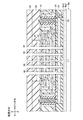
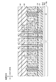
次に、図8〜図14を参照して、第1実施形態に係る不揮発性半導体記憶装置100の製造工程について説明する。ここで、図8、図9A、図10、図11A、図13〜図15は、第1実施形態に係る不揮発性半導体記憶装置100の製造工程を示すロウ方向断面図である。図9B、図11B、及び図12は、第1実施形態に係る不揮発性半導体記憶装置100の製造工程を示す上面図である。なお、図9Bは、図9Aに対応する上面図であり、図11Bは、図11Aに対応する上面図である。
(Manufacturing process of the nonvolatile
Next, with reference to FIGS. 8 to 14, a manufacturing process of the nonvolatile
先ず、図8に示すように、ソース側選択トランジスタ層20を形成し、そのソース側分離絶縁層24上に酸化シリコン(SiO2)を堆積させ、酸化シリコン層81を形成する。
First, as shown in FIG. 8, a source side
次に、図9A、図9Bに示すように、ロウ方向に所定間隔毎に酸化シリコン層81が所定幅だけ残るように、エッチングを施す。そして、エッチング後の酸化シリコン層81の側面に窒化シリコン(SiN)を形成する。これら工程を経て、突出層50が形成される。すなわち、エッチング後の酸化シリコン層81は、柱状層51となる。第1酸化シリコン層81aの側面に形成した窒化シリコンは、側壁層52となる。
Next, as shown in FIGS. 9A and 9B, etching is performed so that the
続いて、図10に示すように、ソース側分離絶縁層24の上面、突出層50の上面及び側面を覆うように、ポリシリコン(p−Si)、酸化シリコン(SiO2)を交互に積層させた後、窒化シリコン(SiN)を堆積させる。この工程により、第1〜第4ポリシリコン層82a〜82d、第1〜第4酸化シリコン層83a〜83d、及び窒化シリコン層84が形成される。
Subsequently, as shown in FIG. 10, polysilicon (p-Si) and silicon oxide (SiO 2) are alternately stacked so as to cover the upper surface of the source-side isolation /
次に、図11A及び図11Bに示すように、化学機械研磨(CMP:Chemical Mechanical Polishing)により突出層50の上面まで、第1〜第4ポリシリコン層82a〜82d、第1〜第4酸化シリコン層83a〜83d、及び窒化シリコン層84を研磨する。この工程を経て、第1〜第4ポリシリコン層82a〜82dは、第1〜第4ワード線導電層31a〜31dとなる。第1〜第4酸化シリコン層83a〜83dは、第1〜第4ワード線間絶縁層32a〜32dとなる。窒化シリコン層84は、メモリ分離絶縁層33となる。なお、図11A及び図11Bに示すCMPの工程において、突出層50の側壁層51(窒化シリコン)は、CMPのストッパーとして機能する。図11A及び図11Bに示す工程を経て、メモリトランジスタ層30が形成される。
Next, as shown in FIGS. 11A and 11B, the first to fourth polysilicon layers 82a to 82d and the first to fourth silicon oxide layers are formed up to the upper surface of the protruding
続いて、図12に示すように、カラム方向に所定ピッチで、メモリトランジスタ層30、突出層50、ソース側選択トランジスタ層20、及び層間絶縁層25を貫通するようにロウ方向に延びる貫通溝84を形成する。さらに、貫通溝84内に酸化シリコン(SiO2)を堆積させ、層間絶縁層85を形成する。
Subsequently, as shown in FIG. 12, through
次に、図13に示すように、酸化シリコン(SiO2)を堆積させる。そして、メモリトランジスタ層30の上部に整合する位置にポリシリコン(p−Si)を堆積させる。上記工程により、ドレイン側第1絶縁層41、及びドレイン側導電層42が形成される。
Next, as shown in FIG. 13, silicon oxide (SiO 2 ) is deposited. Then, polysilicon (p-Si) is deposited at a position matching the upper portion of the
続いて、図14に示すように、酸化シリコン(SiO2)を堆積させ、ドレイン側第2絶縁層43、層間絶縁層44、及び層間絶縁層61を形成する。そして、層間絶縁層61、ドレイン側第2絶縁層43、ドレイン側導電層42、ドレイン側第1絶縁層41、メモリトランジスタ層30、及びソース側選択トランジスタ層20を貫通するようにホール86を形成する。ホール86は、ソース側ホール26、メモリホール34、ドレイン側ホール46、及び第1コンタクトホール71aとして機能する。
Subsequently, as shown in FIG. 14, silicon oxide (SiO 2 ) is deposited to form the drain side second insulating
次に、図15に示すように、ソース側ホール26に面する側壁に、酸化シリコン(SiO2)、及びポリシリコン(p−Si)を堆積させ、ソース側ゲート絶縁層27、及びソース側柱状半導体層28を形成する。また、メモリホール34に面する側壁に、酸化シリコン(SiO2)、窒化シリコン(SiN)、酸化シリコン(SiO2)、及びポリシリコン(p−Si)を堆積させ、メモリゲート絶縁層35(トンネル絶縁層35a、電荷蓄積層35b、ブロック絶縁層35c)、及びメモリ柱状半導体層36を形成する。また、ドレイン側ホール45に面する側壁に、酸化シリコン(SiO2)、ポリシリコン(p−Si)を堆積させ、ドレイン側ゲート絶縁層46、及びドレイン側柱状半導体層47を形成する。
Next, as shown in FIG. 15, silicon oxide (SiO 2 ) and polysilicon (p-Si) are deposited on the side wall facing the
図15に示す工程に続いて、第2〜第7コンタクトホール71b〜71gを形成し、第1〜第7コンタクトホール71a〜71gを埋めるようにチタン(Ti)/窒化チタン(TiN)、及びタングステン(W)を積層させ、コンタクト層72を形成する。次に、酸化シリコン(SiO2)を堆積させ、層間絶縁層62を形成する。そして、層間絶縁層62を貫通するように第1〜第7溝75a〜75gを形成し、それら第1〜第7溝75a〜75gを埋めるようにチタン(Ti)/窒化チタン(TiN)、及びタングステン(W)を積層させ、配線層76を形成する。以上の工程を経て、図4に示す第1実施形態に係る不揮発性半導体記憶装置100が形成される。
Following the step shown in FIG. 15, second to seventh contact holes 71b to 71g are formed, and titanium (Ti) / titanium nitride (TiN) and tungsten are formed so as to fill the first to
(第1実施形態に係る不揮発性半導体記憶装置100の効果)
次に、第1実施形態に係る不揮発性半導体記憶装置100の効果について説明する。上記のように第1実施形態に係る不揮発性半導体記憶装置100において、第1〜第4ワード線導電層31a〜31dは、半導体基板Baに対して平行に延びる第1〜第4底部311a〜311dと、その第1〜第4底部311a〜311dのロウ方向の端部にて突出層30に沿って半導体基板Baに対して直交方向上方に延びる第1〜第4側部312a〜312dとを備える。第1〜第4側部312a〜312dの上面は、同一平面内に揃えて形成されている。第1〜第4側部312a〜312dは、ロウ方向に第1〜第4ワード線間絶縁層32a〜32dを設けて形成されている。よって、コンタクト層72は、同一平面の第1〜第4側部312a〜312dの上面に接するように形成すれば良いので、コンタクト層72の径は、所定の径よりも大きくする必要はない。コンタクト層72は、第1〜第4ワード線間絶縁層32a〜32dの間隔をもって形成される。したがって、第1実施形態に係る不揮発性半導体記憶装置100は、ワード線導電層の端部を階段状に形成する従来例よりも、その占有面積を縮小化することができる。
(Effect of Nonvolatile
Next, effects of the nonvolatile
また、第1実施形態に係る突出層50のロウ方向の幅は、その突出層50の積層方向の長さ以下である(アスペクト比が1以上)ので、メモリトランジスタ層30の形成過程において、第1実施形態に係る突出層50の上部に積層される層(図10参照)の体積は小さい。この突出層30の上部に積層される層は、CMPによる研磨が必要とされる層である。一般に、CMPにおいては、機械的研磨が行われる。よって、突出層50の研磨速度は高く、その他、平坦な箇所や窪んだ箇所の研磨速度は比較的低い。本発明に係る第1実施形態のように、アスペクト比が高く、突出層50の体積が小さい場合、突出層50上に積層された層は、高い研磨速度で除去される。したがって、第1実施形態に係る不揮発性半導体記憶装置は、第1〜第4導電層31a〜31dと第1〜第4ワード線間絶縁層32a〜32dという異種層の積層構造を持ちながら、比較的容易に平坦となるように、それらを選択的に除去することが可能である。
In addition, since the width in the row direction of the protruding
[第2実施形態]
(第2実施形態に係る不揮発性半導体記憶装置100aの具体的構成)
次に、図16を参照して、第2実施形態に係る不揮発性半導体記憶装置100aの具体的構成を説明する。図16は、第2実施形態に係る不揮発性半導体記憶装置100aのロウ方向の断面図である。なお、第2実施形態において、第1実施形態と同様の構成については、同一符号を付し、その説明を省略する。
[Second Embodiment]
(Specific Configuration of Nonvolatile
Next, a specific configuration of the nonvolatile
第2実施形態に係る不揮発性半導体記憶装置100aは、第1実施形態と異なる突出層50A、及びメモリトランジスタ層30Aを有する。
The nonvolatile
突出層50Aは、台形状に形成されている。つまり、突出層50Aの下面は、突出層50Aの上面よりも大きく形成されている。突出層50Aは、台形状の柱状層51A、及びその側壁に形成された側壁層52Aを有する。柱状層51Aは、酸化シリコン(SiO2)にて構成されている。側壁層52Aは、窒化シリコン(SiN)にて構成されている。
The protruding
メモリトランジスタ層30Aは、第1実施形態と異なる第1〜第4ワード線導電層31aa〜31da,及び第1〜第4ワード線間絶縁層32aa〜32da有する。第1〜第4ワード線導電層31aa〜31daは、第1実施形態と同様の第1〜第4底部311a〜311dを有する。一方、第1〜第4ワード線導電層31aa〜31daは、第1実施形態と異なる第1〜第4側部313a〜313dを有する。第1〜第4側部313a〜313dは、第1〜第4底部311a〜311dのロウ方向の端部にて突出層50Aに沿って半導体基板Baに対して所定の角度をもって傾斜して上方に延びるように形成されている。第1〜第4ワード線間絶縁層32aa〜32daは、上記形状を有する第1〜第4ワード線導電層31aa〜31daの間に形成されている。
The
(第2実施形態に係る不揮発性半導体記憶装置100aの効果)
次に、第2実施形態に係る不揮発性半導体記憶装置100aの効果について説明する。第2実施形態に係る不揮発性半導体記憶装置100aは、第1実施形態と略同様の構成を有する。したがって、第2実施形態に係る不揮発性半導体記憶装置100aは、第1実施形態と同様の効果を奏する。
(Effect of Nonvolatile
Next, effects of the nonvolatile
さらに、第2実施形態に係る不揮発性半導体記憶装置100aにおいて、第1〜第4ワード線導電層31aa〜31daは、第1実施形態と異なり、突出層50Aに沿って半導体基板Baに対して所定の角度をもって傾斜して上方に延びる第1〜第4側部313a〜313dを有する。したがって、その第1〜第4側部313a〜313dの上面は、第1実施形態よりも広い面積を有する。これにより、第2実施形態に係る不揮発性半導体記憶装置100aにおいて、コンタクト層72は、第1実施形態よりも容易に、第1〜第4ワード線導電層31aa〜31daに接するように形成することができる。
Further, in the nonvolatile
[第3実施形態]
(第3実施形態に係る不揮発性半導体記憶装置100bの具体的構成)
次に、図17A〜図17Dを参照して、第3実施形態に係る不揮発性半導体記憶装置100bの具体的構成を説明する。図17Aは、第3実施形態に係る不揮発性半導体記憶装置100bのメモリトランジスタ層30Bの概略上面図である。図17Bは、図17AのA部拡大図である。図17Cは、メモリトランジスタ層30B、コンタクト層72a、及び配線層76aを示す上面概略図である。図17Dは、各第1〜第4ワード線導電層31ab〜31dbを示す上面概略図である。なお、第3実施形態において、第1及び第2実施形態と同様の構成については、同一符号を付し、その説明を省略する。
[Third Embodiment]
(Specific Configuration of Nonvolatile
Next, a specific configuration of the nonvolatile
図17A〜図17D示すように、第3実施形態に係る不揮発性半導体記憶装置100bは、第1及び第2実施形態と異なるメモリトランジスタ層30B、及び突出層50Bを有する。
As illustrated in FIGS. 17A to 17D, the nonvolatile
メモリトランジスタ層30Bは、第1及び第2実施形態と異なる第1〜第4ワード線導電層31ab〜31db、及び第1〜第4ワード線間絶縁層32ab〜32dbを有する。
The
突出層50Bは、半径R5をもって円柱状に形成されている。突出層50Bの直径(半径R5の2倍)は、突出層50Bの積層方向の高さ以下である。すなわち、第1実施形態と同様に、ロウ方向の突出層50Bの幅は、積層方向突出層50Bの長さ以下である。
The protruding
突出層50Bは、円柱状の柱状層51B、及び柱状層51Bの側壁に形成された側壁層52Bを有する。柱状層51Bは、酸化シリコン(SiO2)にて構成されている。側壁層52Bは、窒化シリコン(SiN)にて構成されている。突出層50Bは、ロウ方向及びカラム方向にマトリクス状に形成されている。突出層50Bは、第1〜第4ワード線導電層31ab〜31dbにて囲まれるように形成されている。
The protruding
第1〜第4ワード線導電層31ab〜31dbは、突出層50Bを取り囲むように形成されている。第1〜第4ワード線導電層31ab〜31dbは、上面に開口を有する帽子状に形成されている。第1〜第4ワード線導電層31ab〜31dbは、第1〜第4円筒部(第1〜第4側部)314a〜314d、及び第1〜第4鍔部(第1〜第4底部)315a〜315dを有する。
The first to fourth word line conductive layers 31ab to 31db are formed so as to surround the
第1〜第4円筒部314a〜314dは、円筒状に形成されている。第1〜第4円筒部314a〜314dは、第1〜第4鍔部315a〜315dの端部から突出層50Bに沿って半導体基板Baに対して直交方向上方に延びるように形成されている。第1〜第4円筒部314a〜314dは、それらの中心軸が突出層50Bの中心と一致するように形成されている。第1円筒部314aの内径R11は、突出層50Bの半径R5よりも大きくなるように形成されている。第2円筒部314bの内径R21は、第1円筒部314aの外径R12よりも大きくなるように形成されている。第3円筒部314cの内径R31は、第2円筒部314bの外径R22よりも大きくなるように形成されている。第4円筒部314dの内径R41は、第3円筒部314cの外径R32よりも大きくなるように形成されている。第1〜第4円筒部314a〜314dの上面は、上方からみてドーナツ状に形成されている。第1〜第4円筒部314a〜314dの上面は、同一平面内に揃うように形成されている。
The first to fourth
第1〜第4鍔部315a〜315dは、鍔状に形成されている。第1〜第4鍔部315a〜315dは、半導体基板Baと平行に延びるように形成されている。第1〜第4鍔部315a〜315dは、上方からみてロウ方向に長手を有する略矩形板状に形成されている。また、第1〜第4鍔部315a〜315dは、第1〜第4円筒部314a〜314dと接する位置にその端部を有する。
The first to
第1〜第4ワード線間絶縁層32ab〜32dbは、第1〜第4ワード線導電層31ab〜31adの間に設けられている。 The first to fourth inter-wordline insulating layers 32ab to 32db are provided between the first to fourth wordline conductive layers 31ab to 31ad.
また、不揮発性半導体記憶装置100bは、第1及び第2実施形態と異なるンタクト層72a、及び配線層76aを有する。コンタクト層72aは、上方からみて円形状(ドーナツ状)に形成された第1〜第4ワード線導電層32ab〜32dbの第1〜第4円筒部314a〜314dの上面に接するように形成されている。配線層76aは、各コンタクト層72aに接するようにカラム方向に延びるように形成されている。
Further, the nonvolatile
(第3実施形態に係る不揮発性半導体記憶装置100bの製造工程)
次に、図18〜図20を参照して、第3実施形態に係る不揮発性半導体記憶装置100bの製造工程について説明する。ここで、図18〜図20は、第3実施形態に係る不揮発性半導体記憶装置100bの製造工程を示す上面図である。
(Manufacturing process of the nonvolatile
Next, with reference to FIGS. 18-20, the manufacturing process of the non-volatile
先ず、第3実施形態に係る不揮発性半導体記憶装置100bにおいては、第1実施形態の図8と同様の工程を行う。
First, in the nonvolatile
続いて、図18に示すように、ロウ方向及びカラム方向に所定間隔毎(マトリクス状)に且つ円柱状に酸化シリコン層81が所定幅だけ残るように、エッチングを施す。そして、エッチング後の酸化シリコン層81の側面に窒化シリコン(SiN)を形成する。これら工程を経て、突出層50Bが形成される。すなわち、エッチング後の酸化シリコン層81は、円柱状の柱状層51Bとなる。また、酸化シリコン層81の側面に形成した窒化シリコンは、側壁層52Bとなる。
Subsequently, as shown in FIG. 18, etching is performed so that the
次に、第1実施形態の図10と同様の工程を経た後、図19に示すように、突出層50Bを取り囲むように第1〜第4ワード線導電層31ab〜31db、第1〜第4ワード線間絶縁層32ab〜32db、及びメモリ分離絶縁層33を形成する。
Next, after the same steps as in FIG. 10 of the first embodiment, as shown in FIG. 19, the first to fourth word line conductive layers 31ab to 31db and the first to fourth so as to surround the
続いて、図20に示すように、突出層50Bの間にロウ方向に延びる第1の貫通溝84Aを形成する。また、突出層50Bの間にカラム方向に延びる第2の貫通溝84Bを形成する。第1の貫通溝84A、及び第2の貫通溝84Bは、メモリ分離絶縁層33、第1〜第4ワード線導電層31ab〜31db、第1〜第4ワード線間絶縁層32ab〜32db、及びソース側選択トランジスタ層20を貫通するように形成する。そして、第1の貫通溝84A、及び第2の貫通溝84Bを埋めるように酸化シリコン(SiO2)を堆積させ、層間絶縁層85A、85Bを形成する。図19に示す工程の後、第1実施形態の図13〜図15と同様の工程を行い、図17A〜図17Dに示す第4実施形態に係る不揮発性半導体記憶装置100bを形成する。
Subsequently, as shown in FIG. 20, a first through
上記製造工程により、突出層50Bは、第1、第2の貫通孔84A、84Bがつくる閉曲線の中に含まれることとなる。すなわち、突出層50Bは、第1、第2の貫通孔84A、84Bと交わらない。
Through the above manufacturing process, the protruding
(第3実施形態に係る不揮発性半導体記憶装置100bの効果)
次に、第3実施形態に係る不揮発性半導体記憶装置100bの効果について説明する。第3実施形態に係る不揮発性半導体記憶装置100bは、第1実施形態と略同様の構成を有する。したがって、第3実施形態に係る不揮発性半導体記憶装置100bは、第1実施形態と同様の効果を奏する。
(Effects of Nonvolatile
Next, effects of the nonvolatile
さらに、第3実施形態に係る不揮発性半導体記憶装置100bは、第1実施形態と異なる円柱状の突出層50B、及びその円柱状の突出層50Bを囲むように形成された第1〜第4ワード線導電層31ab〜31dbを有する。ここで、第3実施形態の効果を説明するため、上述した第1実施形態と比較する。第1実施形態に係る不揮発性半導体記憶装置100の製造工程において、突出層50は、図12に示すように、貫通溝84を形成する際に削られる。第1実施形態において、貫通溝84は、突出層50を含む不均一な層に亘って形成される。つまり、貫通溝84のエッチングの際、貫通溝84となる底部では、第1〜第4ワード線導電層31a〜31d、第1〜第4ワード線間絶縁層32a〜32dが、時間的に交互に現れる。これに対し、突出層50では、第1〜第4ワード線導電層31a〜31d、第1〜第4ワード線間絶縁層32a〜32dが、同時にエッチングされ続けることとなる。このような関係で、第1実施形態において、貫通溝84の底部を均一な深さに形成することは、RIE技術の高度な組み合わせが必要である。
Further, the nonvolatile
一方、第3実施形態においては、上記図20に示す製造工程に示したように、突出層50Bは,第1の貫通溝84A、及び第2の貫通溝84Bを形成する際に削られることはない。つまり、第3実施形態において、第1の貫通溝84A、及び第2の貫通溝84Bは、第1実施形態よりも均一な層に亘って形成される。つまり、エッチングの際、時間的に交互に、第1〜第4ワード線導電層31ab〜31db、第1〜第4ワード線間絶縁層32ab〜32dbが現れる。よって、RIE技術としては、第1〜第4ワード線導電層31ab〜31db、第1〜第4ワード線間絶縁層32ab〜32dbの選択エッチングを交互に繰り返すことで、容易に均一な深さの第1、第2の貫通溝84A、84Bを形成することが可能である。すなわち、第3実施形態に係る不揮発性半導体記憶装置100bは、第1実施形態よりも容易に製造することができる。
On the other hand, in the third embodiment, as shown in the manufacturing process shown in FIG. 20, the protruding
[第4実施形態]
(第4実施形態に係る不揮発性半導体記憶装置100cの具体的構成)
次に、図21を参照して、第4実施形態に係る不揮発性半導体記憶装置100cの具体的構成を説明する。図21は、第3実施形態における不揮発性半導体記憶装置100bのロウ方向断面図である。なお、第4実施形態において、第1〜第3実施形態と同様の構成については、同一符号を付し、その説明を省略する。
[Fourth Embodiment]
(Specific Configuration of Nonvolatile
Next, a specific configuration of the nonvolatile
図21に示すように、第4実施形態に係る不揮発性半導体記憶装置100cは、第1〜第3実施形態と異なるメモリトランジスタ層30Cを有する。
As shown in FIG. 21, the non-volatile
メモリトランジスタ層30Cは、第1〜第3実施形態と異なる第1〜第4ワード線導電層31ac〜31dcを有する。第1〜第4ワード線導電層31ac〜31dcは、金属(例えば、アルミニウム(Al))を含むように構成されている。なお、第1〜第4ワード線導電層31ac〜31dcは、第1実施形態と同様の形状をもつ第1〜第4底部311a’〜311d’、及び第1〜第4側部312a’〜312d’を有する。
The
(第4実施形態に係る不揮発性半導体記憶装置100cの製造工程)
次に、図22〜図24を参照して、第4実施形態に係る不揮発性半導体記憶装置100cの製造工程について説明する。
(Manufacturing Process of Nonvolatile
Next, with reference to FIGS. 22 to 24, a manufacturing process of the nonvolatile
先ず、第1実施形態の図15に示す工程まで行う。続いて、ドレイン側ホール46の上方に位置する第1コンタクトホール71a内を埋めるように、酸化シリコン(SiO2)を堆積させる。この工程により、ドレイン側柱状半導体層47の上方にも、層間絶縁層61が形成される。
First, the steps up to the step shown in FIG. 15 of the first embodiment are performed. Subsequently, silicon oxide (SiO 2 ) is deposited so as to fill the
続いて、図22に示すように、第1〜第4ワード線導電層31a〜31dの側部312a〜312dの上面を露出させるように溝87を形成する。次に、図23に示すように、溝87内に、5nm程度のチタン(Ti)層88、及びアルミニウム(Al)層89を堆積させる。
Subsequently, as shown in FIG. 22, a
続いて、図24に示すように、熱処理することで、アルミニウム層89からポリシリコンにて構成された第1〜第4ワード線導電層31a〜31dにアルミニウムを多量に含有させる。この工程により、第4実施形態に係る金属を含む第1〜第4ワード線導電層31ac〜31adが形成される。図23に示す工程に続き、溝87を酸化シリコン(SiO2)にて埋めた後、第1実施形態と同様の工程を行なうことにより、図21に示す第4実施形態に係る不揮発性半導体記憶装置100cが形成される。
Next, as shown in FIG. 24, a large amount of aluminum is contained in the first to fourth word line
(第4実施形態に係る不揮発性半導体記憶装置100cの効果)
次に、第4実施形態に係る不揮発性半導体記憶装置100cの効果について説明する。第4実施形態に係る不揮発性半導体記憶装置100cは、第1実施形態と略同様の構成を有する。したがって、第4実施形態に係る不揮発性半導体記憶装置100cは、第1実施形態と同様の効果を奏する。
(Effect of Nonvolatile
Next, effects of the nonvolatile
さらに、第4実施形態に係る不揮発性半導体記憶装置100cにおいて、第1〜第4ワード線導電層31ac〜31dcは、金属(例えば、アルミニウム(Al))を含むように構成されている。したがって、第4実施形態に係る不揮発性半導体記憶装置100cにおける第1〜第4ワード線導電層31ac〜31dcは、第1実施形態よりも低抵抗とすることができる。
Furthermore, in the nonvolatile
また、第1〜第4ワード線導電層31ac〜31dcは、第1実施形態と同様に第1〜第4側部312a’〜312d’を有する。したがって、図22に示す工程のように、第4実施形態に係る不揮発性半導体記憶装置100cは、第1〜第4側部312a’〜312d’の上面にてアルミニウム層89と第1〜第4ワード線導電層31ac〜31dcとを接触させることができる。
The first to fourth word line conductive layers 31ac to 31dc have first to
[第5実施形態]
(第5実施形態に係る不揮発性半導体記憶装置100dの具体的構成)
次に、図25及び図26を参照して、第5実施形態に係る不揮発性半導体記憶装置100dの具体的構成を説明する。図25は、第5実施形態に係る不揮発性半導体記憶装置100dの
ロウ方向断面図である。図26は、図25のB部拡大図である。なお、第5実施形態において、第1〜第4実施形態と同様の構成については、同一符号を付し、その説明を省略する。
[Fifth Embodiment]
(Specific Configuration of Nonvolatile
Next, a specific configuration of the nonvolatile
図25に示すように、第5実施形態に係る不揮発性半導体記憶装置100dは、第1〜第4実施形態と異なる突出層50C、及びメモリトランジスタ層30Dを有する。
As shown in FIG. 25, the nonvolatile
突出層50Cは、階段状に、且つその突出層50Cのロウ方向の幅が下層から上層へと大きくなるように形成されている。図26に示すように、突出層50Cは、第1突出層50C1、及び第2突出層50C2にて構成されている。第1突出層50C1は、第1実施形態の突出層50と同様の構成を有する。第2突出層50C2は、第1突出層50C1の上部に形成されている。ロウ方向の第2突出層50C2の幅は、ロウ方向第1突出層50C1の幅よりも大きくなるように形成されている。
The protruding
メモリトランジスタ層30Dは、第1実施形態と同様に、ソース側選択トランジスタ層20の上面に、第1〜第4ワード線導電層31a〜31d、第1〜第4ワード線間絶縁層32a〜32d、及びメモリ分離絶縁層33の積層構造を有する。さらに、メモリトランジスタ層30Dは、メモリ保護絶縁層33上に、交互に積層された第5〜第8ワード線導電層31e〜31h、第5〜第8ワード線間絶縁層32e〜32h、及びメモリ分離絶縁層33aの積層構造を有する。
Similar to the first embodiment, the
第1〜第4ワード線導電層31a〜31d、第1〜第4ワード線間絶縁層32a〜32d、及びメモリ分離絶縁層33は、第1実施形態と同様に構成されている。すなわち、例えば、第1〜第4ワード線導電層31a〜31dの第1〜第4側部312a〜312dは、第1突出層50C1に沿って半導体基板Baに対して直交上方に延びるように形成されている。
The first to fourth word line
第5〜第8ワード線導電層31e〜31hは、図24に示す断面形状にて、上方に開口を向ける「コの字」状(凹型)となるように形成されている。第5〜第8ワード線導電層31e〜31hは、第5〜第8底部311e〜311h、及び第5〜第8側部312e〜312hを有する。
The fifth to eighth word line
第5〜第8底部311e〜311hは、半導体基板Baに対して平行に延びるように形成されている。第5底部311eのロウ方向の幅は、第4底部311dのロウ方向の幅よりも短い。第6底部311fのロウ方向の幅は、第5底部311eのロウ方向の幅よりも短い。第7底部311gのロウ方向の幅は、第6底部311fのロウ方向の幅よりも短い。第8底部311hのロウ方向の幅は、第7底部311fのロウ方向の幅よりも短い。
The fifth to
第5〜第8側部312e〜312hは、第5〜第8底部311e〜311hのロウ方向の端部にて第2突出層50C2に沿って半導体基板Baに対して直交方向上方に延びるように形成されている。第5〜第8側部312e〜312hの上面は、所定の高さで揃うように形成されている。
The fifth to
また、メモリトランジスタ層30Dは、第1〜第4実施形態と異なるメモリホール34’、メモリゲート絶縁層35’、及びメモリ柱状半導体層36’を有する。メモリホール34’は、メモリ分離絶縁層33a、メモリ分離絶縁層33、第1〜第8ワード線導電層31a〜31h、第1〜第8ワード線間絶縁層32a〜32hを貫通するように形成されている。メモリゲート絶縁層35’は、このメモリホール34’に面する側壁に形成されている。メモリ柱状半導体層36’は、このメモリゲート絶縁層35’に接してメモリホール34’を埋めるように形成されている。
The
また、不揮発性半導体記憶装置100dは、第1〜第4実施形態と異なる第1〜第11コンタクトホール71a’〜71k’を有する。
The nonvolatile
第1コンタクトホール71a’は、ソース側導電層22の上面に達するように形成されている。第1コンタクトホール71a’は、層間絶縁層61、層間絶縁層44、ドレイン側第1絶縁層41、第2突出層50C2、第1突出層50C1、ソース側分離絶縁層24、及びソース側第2絶縁層23を貫通するように形成されている。
The
第2〜第5コンタクトホール71b’〜 71e’は、第1〜第4ワード線導電層31a〜31dの第1〜第4側部312a〜312dの上面に達するように形成されている。第2〜第5コンタクトホール71b’〜 71e’は、層間絶縁層61、層間絶縁層44、ドレイン側第1絶縁層41、及び第2突出層50C2を貫通するように形成されている。
The second to fifth contact holes 71b 'to 71e' are formed to reach the upper surfaces of the first to
第6〜第9コンタクトホール71f’〜 71i’は、第5〜第8ワード線導電層31e〜31hの第5〜第8側部312e〜312hの上面に達するように形成されている。第6〜第9コンタクトホール71f’〜 71i’は、層間絶縁層61、層間絶縁層44、及びドレイン側第1絶縁層41を貫通するように形成されている。
The sixth to
第10コンタクトホール71j’は、ソース側導電層42の上面に達するように形成されている。第10コンタクトホール71j’は、層間絶縁層61、及びドレイン側第2絶縁層43を貫通するように形成されている。
The tenth contact hole 71j ′ is formed so as to reach the upper surface of the source-side conductive layer. The tenth contact hole 71j ′ is formed so as to penetrate the interlayer insulating
第11コンタクトホール71k’は、ドレイン側柱状半導体層47の上面に達するように形成されている。第11コンタクトホール71k’は、層間絶縁層61を貫通するように形成されている。
The eleventh contact hole 71 k ′ is formed so as to reach the upper surface of the drain side
第1〜第11コンタクトホール71a’〜71k’内には、コンタクト層72’が形成されている。コンタクト層72’は、バリアメタル層73’、及びメタル層74’を有する。バリアメタル層73’は、チタン(Ti)/窒化チタン(TiN)にて構成されている。メタル層74’は、タングステン(W)にて構成されている。
A
また、不揮発性半導体記憶装置100dは、第1〜第11コンタクトホール71a’〜71k’に整合する位置に設けられ且つ層間絶縁層62を貫通するように形成された第1〜第11溝75a’〜75k’を有する。第1〜第11溝75a’〜75k’内には、配線層76’が形成されている。
In addition, the nonvolatile
配線層76’は、バリアメタル層77’、及びメタル層78’を有する。バリアメタル層77’は、チタン(Ti)/窒化チタン(TiN)にて構成されている。メタル層78’は、タングステン(W)にて構成されている。
The
(第5実施形態に係る不揮発性半導体記憶装置100dの製造工程)
次に、図27〜図29を参照して、第5実施形態に係る不揮発性半導体記憶装置100dの製造工程について説明する。図27〜図29は、第5実施形態に係る不揮発性半導体記憶装置100dの製造工程を示すロウ方向断面図である。
(Manufacturing Process of Nonvolatile
Next, with reference to FIGS. 27 to 29, a manufacturing process of the nonvolatile
先ず、第1実施形態の図8〜図11A及び図11Bに示す工程を行う。なお、第1実施形態の図8〜図11A及び図11Bに示す工程で形成される突出層50は、第5実施形態の第1突出層50C1として機能する。
First, the steps shown in FIGS. 8 to 11A and 11B of the first embodiment are performed. Note that the protruding
続いて、図27に示すように、第1突出層50C1の上面に第2突出層50C2を形成する。ここで、第2突出層50C2のロウ方向の幅は、第1突出層50C1のロウ方向の幅よりも長くなるように設定する。つまり、図27に示す工程を経て、第1突出層50C1、及び第2突出層50C2にて、階段状に且つそのロウ方向の幅が下層から上層へと大きくなる突出層50Cが形成される。
Subsequently, as shown in FIG. 27, a second protruding layer 50C2 is formed on the upper surface of the first protruding layer 50C1. Here, the width in the row direction of the second protruding layer 50C2 is set to be longer than the width in the row direction of the first protruding layer 50C1. That is, through the steps shown in FIG. 27, the first projecting layer 50C1 and the second projecting layer 50C2 form a projecting
次に、図28に示すように、メモリ分離絶縁層33の上面、第2突出層50C2の上面及び側面を覆うように、ポリシリコン(p−Si)、酸化シリコン(SiO2)を交互に積層させた後、窒化シリコン(SiN)を堆積させる。この工程により、第5〜第8ポリシリコン層82e〜82h、第5〜第8酸化シリコン層83e〜83h、及び窒化シリコン層84aが形成される。
Next, as shown in FIG. 28, polysilicon (p-Si) and silicon oxide (SiO 2 ) are alternately stacked so as to cover the upper surface of the memory
続いて、図29に示すように、CMPにより第2突出層50C2の上面まで、第5〜第8ポリシリコン層82e〜82h、第5〜第8酸化シリコン層83e〜83h、及び窒化シリコン層84aを研磨する。この工程を経て、第5〜第8ポリシリコン層82e〜82hは、第5〜第8ワード線導電層31e〜31hとなる。第5〜第8酸化シリコン層83e〜83hは、第5〜第8ワード線間絶縁層32e〜32hとなる。窒化シリコン層84aは、メモリ分離絶縁層33aとなる。なお、図29に示すCMPの工程において、第2突出層50C2の側壁層52C2(窒化シリコン)は、CMPのストッパーとして機能する。図29に示す工程の後、第1実施形態と同様の工程を経て、図25及び図26に示す第5実施形態に係る不揮発性半導体記憶装置100dが形成される。
Subsequently, as shown in FIG. 29, the fifth to
(第5実施形態に係る不揮発性半導体記憶装置100dの効果)
次に、第5実施形態に係る不揮発性半導体記憶装置100dの効果を説明する。第5実施形態に係る不揮発性半導体記憶装置100dは、第1実施形態と同様の構成を有する。したがって、第5実施形態に係る不揮発性半導体記憶装置100dは、第1実施形態と同様の効果を奏する。
(Effect of Nonvolatile
Next, effects of the nonvolatile
第5実施形態に係る不揮発性半導体記憶装置100dは、第1実施形態の第1〜第4ワード線導電層31a〜31dに加えて、第5〜第8ワード線導電層31e〜31hを有する。したがって、第5実施形態に係る不揮発性半導体記憶装置100dは、第1実施形態よりも高集積化された構造を有する。
The nonvolatile
[その他の実施形態]
以上、不揮発性半導体記憶装置の実施形態を説明してきたが、本発明は、上記実施形態に限定されるものではなく、発明の趣旨を逸脱しない範囲内において種々の変更、追加、置換等が可能である。
[Other Embodiments]
The embodiments of the nonvolatile semiconductor memory device have been described above. However, the present invention is not limited to the above embodiments, and various modifications, additions, substitutions, and the like are possible without departing from the spirit of the invention. It is.
例えば、第5実施形態において、メモリトランジスタ層30Dは、第1〜第8ワード線導電層31a〜31hを設けている。また、突出層50Cは、階段状に、且つその突出層50Cのロウ方向の幅が下層から上層へと大きくなるように形成されており、第1突出層50C1、及び第2突出層50C2にて構成されている(2段の階段状の構成)。しかしながら、本発明は、このような第5実施形態の構成に限られるものではない。メモリトランジスタ層は、さらに複数層(9以上の層)のワード線導電層を有するものであってもよい。突出層は、2段の階段状に限られず、さらに複数段(3段以上)の階段状に形成されていてもよい。
For example, in the fifth embodiment, the
例えば、第3実施形態に係るメモリトランジスタ層30B及び突出層50Bの構成は、第2、第4、及び第5実施形態の構成にも適応可能である。
For example, the configuration of the
100、100a〜100d…不揮発性半導体記憶装置、12…メモリトランジスタ領域、13…ワード線駆動回路、14…ソース側選択ゲート線駆動回路、15…ドレイン側選択ゲート線駆動回路、16…センスアンプ、20…ソース側選択トランジスタ層、30、30A〜30D…メモリトランジスタ層、40…ドレイン側選択トランジスタ層、50、50A〜50C…突出層、Ba…半導体基板、CLmn…柱状半導体、MTr1mn〜MTr4mn…メモリトランジスタ、SSTrmn…ソース側選択トランジスタ、SDTrmn…ドレイン側選択トランジスタ。
DESCRIPTION OF
Claims (5)
基板に対して上方に突出して形成された突出層を備え、
前記メモリストリングスは、
前記基板上に積層された複数の導電層と、
当該複数の導電層を貫通するように形成された半導体層と、
前記導電層と前記半導体層との間に形成され且つ電荷を蓄積可能に構成された電荷蓄積層とを備え、
前記複数の導電層は、
前記基板に対して平行に延びる底部と、
当該底部の端部にて前記突出層に沿って前記基板に対して上方に延びる側部とを備え、
前記基板に平行な第1方向の前記突出層の幅は、積層方向の前記突出層の長さ以下である
ことを特徴とする不揮発性半導体記憶装置。 A non-volatile semiconductor memory device including a memory string including a plurality of memory cells that are electrically rewritable and connected in series,
A protruding layer formed to protrude upward with respect to the substrate;
The memory strings are
A plurality of conductive layers stacked on the substrate;
A semiconductor layer formed so as to penetrate the plurality of conductive layers;
A charge storage layer formed between the conductive layer and the semiconductor layer and configured to store charges;
The plurality of conductive layers are:
A bottom extending parallel to the substrate;
A side portion extending upward with respect to the substrate along the protruding layer at an end of the bottom portion,
A width of the protruding layer in the first direction parallel to the substrate is equal to or less than a length of the protruding layer in the stacking direction.
前記側部は、前記突出層に沿って前記基板に対して所定の角度をもって傾斜して上方に延びるように形成されている
ことを特徴とする請求項1記載の不揮発性半導体記憶装置。 The protruding layer is formed in a trapezoidal shape,
The nonvolatile semiconductor memory device according to claim 1, wherein the side portion is formed so as to incline at a predetermined angle with respect to the substrate along the protruding layer and extend upward.
ことを特徴とする請求項1又は請求項2記載の不揮発性半導体記憶装置。 The nonvolatile semiconductor memory device according to claim 1, wherein the plurality of conductive layers are formed so as to surround the protruding layer.
ことを特徴とする請求項1乃至請求項3のいずれか1項記載の不揮発性半導体記憶装置。 4. The method according to claim 1, wherein the projecting layer is formed in a stepped manner so that a width of the projecting layer in the first direction increases from a lower layer to an upper layer. A nonvolatile semiconductor memory device according to item.
基板に平行な第1方向の幅が積層方向の長さ以下であり且つ前記基板に対して上方に突出する突出層を形成する工程と、
前記基板上に前記突出層を覆うように複数の導電層を積層する工程と、
積層した複数の前記導電層を前記突出層の上面まで平坦化する工程と
を備えることを特徴とする不揮発性半導体記憶装置の製造方法。
A method for manufacturing a nonvolatile semiconductor memory device having a memory string that includes a plurality of memory cells that are electrically rewritable and connected in series,
Forming a projecting layer having a width in a first direction parallel to the substrate being equal to or less than a length in the stacking direction and projecting upward with respect to the substrate;
Laminating a plurality of conductive layers on the substrate so as to cover the protruding layer;
Flattening the plurality of stacked conductive layers to the upper surface of the protruding layer. A method for manufacturing a nonvolatile semiconductor memory device, comprising:
Priority Applications (2)
| Application Number | Priority Date | Filing Date | Title |
|---|---|---|---|
| JP2008269804A JP5388537B2 (en) | 2008-10-20 | 2008-10-20 | Nonvolatile semiconductor memory device and manufacturing method thereof |
| US12/556,242 US8237211B2 (en) | 2008-10-20 | 2009-09-09 | Non-volatile semiconductor storage device and method of manufacturing the same |
Applications Claiming Priority (1)
| Application Number | Priority Date | Filing Date | Title |
|---|---|---|---|
| JP2008269804A JP5388537B2 (en) | 2008-10-20 | 2008-10-20 | Nonvolatile semiconductor memory device and manufacturing method thereof |
Publications (2)
| Publication Number | Publication Date |
|---|---|
| JP2010098235A true JP2010098235A (en) | 2010-04-30 |
| JP5388537B2 JP5388537B2 (en) | 2014-01-15 |
Family
ID=42107961
Family Applications (1)
| Application Number | Title | Priority Date | Filing Date |
|---|---|---|---|
| JP2008269804A Expired - Fee Related JP5388537B2 (en) | 2008-10-20 | 2008-10-20 | Nonvolatile semiconductor memory device and manufacturing method thereof |
Country Status (2)
| Country | Link |
|---|---|
| US (1) | US8237211B2 (en) |
| JP (1) | JP5388537B2 (en) |
Cited By (5)
| Publication number | Priority date | Publication date | Assignee | Title |
|---|---|---|---|---|
| US8633104B2 (en) | 2011-07-11 | 2014-01-21 | Samsung Electronics Co., Ltd. | Methods of manufacturing three-dimensional semiconductor devices |
| US8884356B2 (en) | 2012-09-05 | 2014-11-11 | Kabushiki Kaisha Toshiba | Nonvolatile semiconductor memory device and method for manufacturing same |
| US9953993B2 (en) | 2016-07-25 | 2018-04-24 | Toshiba Memory Corporation | Semiconductor memory device |
| US10115627B2 (en) | 2016-08-31 | 2018-10-30 | Toshiba Memory Corporation | Semiconductor device |
| US10262936B2 (en) | 2017-02-08 | 2019-04-16 | Toshiba Memory Corporation | Semiconductor device and manufacturing method thereof |
Families Citing this family (23)
| Publication number | Priority date | Publication date | Assignee | Title |
|---|---|---|---|---|
| JP5388537B2 (en) * | 2008-10-20 | 2014-01-15 | 株式会社東芝 | Nonvolatile semiconductor memory device and manufacturing method thereof |
| JP4922370B2 (en) * | 2009-09-07 | 2012-04-25 | 株式会社東芝 | Nonvolatile semiconductor memory device and manufacturing method thereof |
| JP5259552B2 (en) | 2009-11-02 | 2013-08-07 | 株式会社東芝 | Nonvolatile semiconductor memory device and driving method thereof |
| JP5297342B2 (en) * | 2009-11-02 | 2013-09-25 | 株式会社東芝 | Nonvolatile semiconductor memory device |
| KR101559958B1 (en) * | 2009-12-18 | 2015-10-13 | 삼성전자주식회사 | 3 3 Method for manufacturing three dimensional semiconductor device and three dimensional semiconductor device manufactured by the method |
| JP5670704B2 (en) | 2010-11-10 | 2015-02-18 | 株式会社東芝 | Nonvolatile semiconductor memory device and manufacturing method thereof |
| JP2012204430A (en) * | 2011-03-24 | 2012-10-22 | Toshiba Corp | Nonvolatile semiconductor memory device and method of manufacturing the same |
| JP5411193B2 (en) * | 2011-03-25 | 2014-02-12 | 株式会社東芝 | Method for manufacturing nonvolatile semiconductor memory device |
| KR101808822B1 (en) | 2011-08-04 | 2017-12-14 | 삼성전자주식회사 | Semiconductor devices and methods for fabricating the same |
| JP2013055142A (en) * | 2011-09-01 | 2013-03-21 | Toshiba Corp | Nonvolatile semiconductor memory device |
| KR101865566B1 (en) * | 2011-09-08 | 2018-06-11 | 삼성전자주식회사 | Methods of manufacturing a vertical memory device |
| KR102024723B1 (en) | 2013-01-02 | 2019-09-24 | 삼성전자주식회사 | Three dimensional semiconductor device |
| US8981567B2 (en) | 2013-03-13 | 2015-03-17 | Macronix International Co., Ltd. | 3-D IC device with enhanced contact area |
| KR102083483B1 (en) * | 2013-08-12 | 2020-03-02 | 에스케이하이닉스 주식회사 | Semiconductor memory device and method of manufacturing the same |
| KR20150021742A (en) * | 2013-08-21 | 2015-03-03 | 에스케이하이닉스 주식회사 | Semiconductor device and method of manufacturing the same |
| JP2016035991A (en) | 2014-08-04 | 2016-03-17 | 株式会社東芝 | Semiconductor memory and manufacturing method thereof |
| US9608001B2 (en) | 2015-03-13 | 2017-03-28 | Kabushiki Kaisha Toshiba | Semiconductor memory device |
| US9698150B2 (en) | 2015-10-26 | 2017-07-04 | Kabushiki Kaisha Toshiba | Semiconductor memory device and method for manufacturing the same |
| KR20170130009A (en) | 2016-05-17 | 2017-11-28 | 삼성전자주식회사 | Three-Dimensional Semiconductor Device |
| KR102613511B1 (en) | 2016-06-09 | 2023-12-13 | 삼성전자주식회사 | Integrated circuit device including vertical memory device and method of manufacturing the same |
| KR102650995B1 (en) | 2016-11-03 | 2024-03-25 | 삼성전자주식회사 | Vertical type memory device |
| KR102635182B1 (en) | 2018-07-12 | 2024-02-08 | 삼성전자주식회사 | Semiconductor Memory Device |
| JP2021136270A (en) * | 2020-02-25 | 2021-09-13 | キオクシア株式会社 | Semiconductor storage device and method for manufacturing the same |
Citations (7)
| Publication number | Priority date | Publication date | Assignee | Title |
|---|---|---|---|---|
| JPH05326952A (en) * | 1992-05-21 | 1993-12-10 | Toshiba Corp | Semiconductor device and its production |
| JPH08330586A (en) * | 1995-05-26 | 1996-12-13 | Samsung Electron Co Ltd | Vertical transistor and its manufacture |
| JP2007266143A (en) * | 2006-03-27 | 2007-10-11 | Toshiba Corp | Non-volatile semiconductor memory device and manufacturing method therefor |
| JP2008103429A (en) * | 2006-10-17 | 2008-05-01 | Toshiba Corp | Non-volatile semiconductor storage device and manufacturing method thereof |
| JP2008192857A (en) * | 2007-02-05 | 2008-08-21 | Toshiba Corp | Nonvolatile semiconductor storage device and manufacturing method therefor |
| JP2008244485A (en) * | 2007-03-27 | 2008-10-09 | Samsung Electronics Co Ltd | Non-volatile memory element and manufacturing method thereof |
| US20080253183A1 (en) * | 2007-04-11 | 2008-10-16 | Makoto Mizukami | Semiconductor memory device |
Family Cites Families (18)
| Publication number | Priority date | Publication date | Assignee | Title |
|---|---|---|---|---|
| US96682A (en) * | 1869-11-09 | Improvement in hose-pipes | ||
| JP3403231B2 (en) * | 1993-05-12 | 2003-05-06 | 三菱電機株式会社 | Semiconductor device and manufacturing method thereof |
| US5990509A (en) * | 1997-01-22 | 1999-11-23 | International Business Machines Corporation | 2F-square memory cell for gigabit memory applications |
| US6897116B2 (en) * | 2003-09-12 | 2005-05-24 | United Microelectronics Corp. | Method and structure to improve the gate coupling ratio (GCR) for manufacturing a flash memory device |
| US20050199937A1 (en) * | 2004-03-11 | 2005-09-15 | Chang Augustine W. | 3D flash EEPROM cell and methods of implementing the same |
| US7271063B2 (en) * | 2005-10-13 | 2007-09-18 | Elite Semiconductor Memory Technology, Inc. | Method of forming FLASH cell array having reduced word line pitch |
| JP4817984B2 (en) * | 2006-06-20 | 2011-11-16 | 株式会社東芝 | Nonvolatile semiconductor memory device and manufacturing method thereof |
| KR20080010900A (en) * | 2006-07-28 | 2008-01-31 | 삼성전자주식회사 | Non-volatile memory device, method of operating the same and method of fabricating the same |
| US7821045B2 (en) * | 2006-12-28 | 2010-10-26 | Intel Corporation | Apparatus, system, and method for multiple-segment floating gate |
| JP2008172164A (en) * | 2007-01-15 | 2008-07-24 | Toshiba Corp | Semiconductor device |
| US7795080B2 (en) * | 2007-01-15 | 2010-09-14 | Sandisk Corporation | Methods of forming integrated circuit devices using composite spacer structures |
| KR101283539B1 (en) * | 2007-08-29 | 2013-07-15 | 삼성전자주식회사 | Inverted non-volatile memory devices, stack modules and method of fabricating the same |
| JP5142692B2 (en) | 2007-12-11 | 2013-02-13 | 株式会社東芝 | Nonvolatile semiconductor memory device |
| US7910973B2 (en) * | 2008-03-17 | 2011-03-22 | Kabushiki Kaisha Toshiba | Semiconductor storage device |
| US7915664B2 (en) * | 2008-04-17 | 2011-03-29 | Sandisk Corporation | Non-volatile memory with sidewall channels and raised source/drain regions |
| JP5112201B2 (en) * | 2008-07-11 | 2013-01-09 | 株式会社東芝 | Nonvolatile semiconductor memory device |
| JP5388537B2 (en) * | 2008-10-20 | 2014-01-15 | 株式会社東芝 | Nonvolatile semiconductor memory device and manufacturing method thereof |
| JP5388600B2 (en) * | 2009-01-22 | 2014-01-15 | 株式会社東芝 | Method for manufacturing nonvolatile semiconductor memory device |
-
2008
- 2008-10-20 JP JP2008269804A patent/JP5388537B2/en not_active Expired - Fee Related
-
2009
- 2009-09-09 US US12/556,242 patent/US8237211B2/en active Active
Patent Citations (7)
| Publication number | Priority date | Publication date | Assignee | Title |
|---|---|---|---|---|
| JPH05326952A (en) * | 1992-05-21 | 1993-12-10 | Toshiba Corp | Semiconductor device and its production |
| JPH08330586A (en) * | 1995-05-26 | 1996-12-13 | Samsung Electron Co Ltd | Vertical transistor and its manufacture |
| JP2007266143A (en) * | 2006-03-27 | 2007-10-11 | Toshiba Corp | Non-volatile semiconductor memory device and manufacturing method therefor |
| JP2008103429A (en) * | 2006-10-17 | 2008-05-01 | Toshiba Corp | Non-volatile semiconductor storage device and manufacturing method thereof |
| JP2008192857A (en) * | 2007-02-05 | 2008-08-21 | Toshiba Corp | Nonvolatile semiconductor storage device and manufacturing method therefor |
| JP2008244485A (en) * | 2007-03-27 | 2008-10-09 | Samsung Electronics Co Ltd | Non-volatile memory element and manufacturing method thereof |
| US20080253183A1 (en) * | 2007-04-11 | 2008-10-16 | Makoto Mizukami | Semiconductor memory device |
Cited By (7)
| Publication number | Priority date | Publication date | Assignee | Title |
|---|---|---|---|---|
| US8633104B2 (en) | 2011-07-11 | 2014-01-21 | Samsung Electronics Co., Ltd. | Methods of manufacturing three-dimensional semiconductor devices |
| US8884356B2 (en) | 2012-09-05 | 2014-11-11 | Kabushiki Kaisha Toshiba | Nonvolatile semiconductor memory device and method for manufacturing same |
| US9953993B2 (en) | 2016-07-25 | 2018-04-24 | Toshiba Memory Corporation | Semiconductor memory device |
| US10115627B2 (en) | 2016-08-31 | 2018-10-30 | Toshiba Memory Corporation | Semiconductor device |
| US11004731B2 (en) | 2016-08-31 | 2021-05-11 | Kioxia Corporation | Semiconductor device |
| US11848228B2 (en) | 2016-08-31 | 2023-12-19 | Kioxia Corporation | Semiconductor device |
| US10262936B2 (en) | 2017-02-08 | 2019-04-16 | Toshiba Memory Corporation | Semiconductor device and manufacturing method thereof |
Also Published As
| Publication number | Publication date |
|---|---|
| US8237211B2 (en) | 2012-08-07 |
| US20100096682A1 (en) | 2010-04-22 |
| JP5388537B2 (en) | 2014-01-15 |
Similar Documents
| Publication | Publication Date | Title |
|---|---|---|
| JP5388537B2 (en) | Nonvolatile semiconductor memory device and manufacturing method thereof | |
| JP5253875B2 (en) | Nonvolatile semiconductor memory device and manufacturing method thereof | |
| JP5142692B2 (en) | Nonvolatile semiconductor memory device | |
| JP5193551B2 (en) | Nonvolatile semiconductor memory device and manufacturing method thereof | |
| JP4455615B2 (en) | Nonvolatile semiconductor memory device and manufacturing method thereof | |
| JP5148242B2 (en) | Nonvolatile semiconductor memory device and manufacturing method thereof | |
| JP5364336B2 (en) | Semiconductor memory device | |
| JP5317664B2 (en) | Method for manufacturing nonvolatile semiconductor memory device | |
| JP4649487B2 (en) | Nonvolatile semiconductor memory device and manufacturing method thereof | |
| TWI445164B (en) | Nonvolatile semiconductor memory device | |
| JP2009224612A (en) | Nonvolatile semiconductor memory device and production method thereof | |
| JP2009212280A (en) | Nonvolatile semiconductor storage device and manufacturing method thereof | |
| JP2010080561A (en) | Nonvolatile semiconductor memory device | |
| JP2009200443A (en) | Nonvolatile semiconductor storage device, and its manufacturing method | |
| KR20110093309A (en) | 3d non-volatile memory device and method for manufacturing the same | |
| US11355194B2 (en) | Non-volatile memory device | |
| US8687425B2 (en) | Nonvolatile memory device, method for operating the same, and method for fabricating the same | |
| JP2008103429A (en) | Non-volatile semiconductor storage device and manufacturing method thereof | |
| JP2009224468A (en) | Non-volatile semiconductor memory device | |
| JP2010212518A (en) | Nonvolatile semiconductor memory device | |
| JP2006216957A (en) | Semiconductor device having transistor with vertical gate electrode and method of fabricating the same | |
| JP2009164433A (en) | Nonvolatile semiconductor memory device | |
| JP2011054802A (en) | Nonvolatile semiconductor memory device, and method of manufacturing the same | |
| US20130248975A1 (en) | Non-volatile semiconductor memory device and its manufacturing method | |
| TWI777089B (en) | semiconductor memory device |
Legal Events
| Date | Code | Title | Description |
|---|---|---|---|
| A621 | Written request for application examination |
Free format text: JAPANESE INTERMEDIATE CODE: A621 Effective date: 20110309 |
|
| RD01 | Notification of change of attorney |
Free format text: JAPANESE INTERMEDIATE CODE: A7421 Effective date: 20130221 |
|
| A977 | Report on retrieval |
Free format text: JAPANESE INTERMEDIATE CODE: A971007 Effective date: 20130522 |
|
| A131 | Notification of reasons for refusal |
Free format text: JAPANESE INTERMEDIATE CODE: A131 Effective date: 20130528 |
|
| A521 | Request for written amendment filed |
Free format text: JAPANESE INTERMEDIATE CODE: A523 Effective date: 20130729 |
|
| TRDD | Decision of grant or rejection written | ||
| A01 | Written decision to grant a patent or to grant a registration (utility model) |
Free format text: JAPANESE INTERMEDIATE CODE: A01 Effective date: 20130910 |
|
| A61 | First payment of annual fees (during grant procedure) |
Free format text: JAPANESE INTERMEDIATE CODE: A61 Effective date: 20131008 |
|
| LAPS | Cancellation because of no payment of annual fees |