JP2010044413A - Optical signal transfer method, optical signal relay device, and optical signal storage device - Google Patents
Optical signal transfer method, optical signal relay device, and optical signal storage device Download PDFInfo
- Publication number
- JP2010044413A JP2010044413A JP2009256584A JP2009256584A JP2010044413A JP 2010044413 A JP2010044413 A JP 2010044413A JP 2009256584 A JP2009256584 A JP 2009256584A JP 2009256584 A JP2009256584 A JP 2009256584A JP 2010044413 A JP2010044413 A JP 2010044413A
- Authority
- JP
- Japan
- Prior art keywords
- optical
- optical signal
- light
- wavelength
- signal
- Prior art date
- Legal status (The legal status is an assumption and is not a legal conclusion. Google has not performed a legal analysis and makes no representation as to the accuracy of the status listed.)
- Granted
Links
- 230000003287 optical effect Effects 0.000 title claims abstract description 1457
- 238000000034 method Methods 0.000 title claims abstract description 31
- 238000012546 transfer Methods 0.000 title claims description 40
- 230000003321 amplification Effects 0.000 claims abstract description 190
- 238000003199 nucleic acid amplification method Methods 0.000 claims abstract description 190
- 230000004044 response Effects 0.000 claims abstract description 36
- 239000013307 optical fiber Substances 0.000 claims description 120
- 230000005540 biological transmission Effects 0.000 claims description 87
- 238000009826 distribution Methods 0.000 claims description 64
- 239000004065 semiconductor Substances 0.000 claims description 62
- 238000006243 chemical reaction Methods 0.000 claims description 57
- 230000007423 decrease Effects 0.000 claims description 21
- 239000000284 extract Substances 0.000 claims description 8
- 230000001934 delay Effects 0.000 claims description 5
- 230000008054 signal transmission Effects 0.000 claims description 5
- 229910052761 rare earth metal Inorganic materials 0.000 claims description 4
- 230000008569 process Effects 0.000 abstract description 18
- 230000006870 function Effects 0.000 description 62
- 238000012545 processing Methods 0.000 description 50
- 238000010586 diagram Methods 0.000 description 36
- 239000000835 fiber Substances 0.000 description 32
- 239000010408 film Substances 0.000 description 27
- 239000000758 substrate Substances 0.000 description 20
- 230000008859 change Effects 0.000 description 13
- 230000008901 benefit Effects 0.000 description 12
- 230000009471 action Effects 0.000 description 10
- 230000000694 effects Effects 0.000 description 9
- 238000004891 communication Methods 0.000 description 8
- 239000013078 crystal Substances 0.000 description 7
- JBRZTFJDHDCESZ-UHFFFAOYSA-N AsGa Chemical compound [As]#[Ga] JBRZTFJDHDCESZ-UHFFFAOYSA-N 0.000 description 6
- 238000000605 extraction Methods 0.000 description 6
- 238000000206 photolithography Methods 0.000 description 6
- 239000002096 quantum dot Substances 0.000 description 6
- 229910001218 Gallium arsenide Inorganic materials 0.000 description 5
- 230000002093 peripheral effect Effects 0.000 description 5
- 230000000644 propagated effect Effects 0.000 description 5
- 230000003111 delayed effect Effects 0.000 description 4
- 230000001902 propagating effect Effects 0.000 description 4
- 230000001360 synchronised effect Effects 0.000 description 4
- 230000008878 coupling Effects 0.000 description 3
- 238000010168 coupling process Methods 0.000 description 3
- 238000005859 coupling reaction Methods 0.000 description 3
- 230000003247 decreasing effect Effects 0.000 description 3
- 238000002347 injection Methods 0.000 description 3
- 239000007924 injection Substances 0.000 description 3
- 229910052751 metal Inorganic materials 0.000 description 3
- 239000002184 metal Substances 0.000 description 3
- 239000004038 photonic crystal Substances 0.000 description 3
- 230000009467 reduction Effects 0.000 description 3
- 230000002269 spontaneous effect Effects 0.000 description 3
- GPXJNWSHGFTCBW-UHFFFAOYSA-N Indium phosphide Chemical compound [In]#P GPXJNWSHGFTCBW-UHFFFAOYSA-N 0.000 description 2
- 230000001771 impaired effect Effects 0.000 description 2
- 230000010365 information processing Effects 0.000 description 2
- 239000000463 material Substances 0.000 description 2
- 239000011159 matrix material Substances 0.000 description 2
- 230000010287 polarization Effects 0.000 description 2
- 238000004544 sputter deposition Methods 0.000 description 2
- 239000010409 thin film Substances 0.000 description 2
- 229910052691 Erbium Inorganic materials 0.000 description 1
- 229910000530 Gallium indium arsenide Inorganic materials 0.000 description 1
- WHXSMMKQMYFTQS-UHFFFAOYSA-N Lithium Chemical compound [Li] WHXSMMKQMYFTQS-UHFFFAOYSA-N 0.000 description 1
- 229910004298 SiO 2 Inorganic materials 0.000 description 1
- 229910010413 TiO 2 Inorganic materials 0.000 description 1
- 230000004075 alteration Effects 0.000 description 1
- 238000013459 approach Methods 0.000 description 1
- 230000002238 attenuated effect Effects 0.000 description 1
- 230000000903 blocking effect Effects 0.000 description 1
- 239000003086 colorant Substances 0.000 description 1
- 150000001875 compounds Chemical class 0.000 description 1
- 239000000470 constituent Substances 0.000 description 1
- 238000011161 development Methods 0.000 description 1
- 238000005516 engineering process Methods 0.000 description 1
- UYAHIZSMUZPPFV-UHFFFAOYSA-N erbium Chemical compound [Er] UYAHIZSMUZPPFV-UHFFFAOYSA-N 0.000 description 1
- 230000005284 excitation Effects 0.000 description 1
- 238000002474 experimental method Methods 0.000 description 1
- 239000011521 glass Substances 0.000 description 1
- 230000005764 inhibitory process Effects 0.000 description 1
- 238000002372 labelling Methods 0.000 description 1
- 238000010030 laminating Methods 0.000 description 1
- 229910052744 lithium Inorganic materials 0.000 description 1
- 239000000203 mixture Substances 0.000 description 1
- 230000003534 oscillatory effect Effects 0.000 description 1
- 239000012466 permeate Substances 0.000 description 1
- 230000029553 photosynthesis Effects 0.000 description 1
- 238000010672 photosynthesis Methods 0.000 description 1
- 230000005855 radiation Effects 0.000 description 1
- 150000002910 rare earth metals Chemical class 0.000 description 1
- 230000004043 responsiveness Effects 0.000 description 1
- 230000000630 rising effect Effects 0.000 description 1
- 229920006395 saturated elastomer Polymers 0.000 description 1
- 239000000126 substance Substances 0.000 description 1
- 238000011144 upstream manufacturing Methods 0.000 description 1
- 238000007740 vapor deposition Methods 0.000 description 1
- 238000004804 winding Methods 0.000 description 1
Images


Classifications
-
- G—PHYSICS
- G02—OPTICS
- G02F—OPTICAL DEVICES OR ARRANGEMENTS FOR THE CONTROL OF LIGHT BY MODIFICATION OF THE OPTICAL PROPERTIES OF THE MEDIA OF THE ELEMENTS INVOLVED THEREIN; NON-LINEAR OPTICS; FREQUENCY-CHANGING OF LIGHT; OPTICAL LOGIC ELEMENTS; OPTICAL ANALOGUE/DIGITAL CONVERTERS
- G02F2/00—Demodulating light; Transferring the modulation of modulated light; Frequency-changing of light
- G02F2/004—Transferring the modulation of modulated light, i.e. transferring the information from one optical carrier of a first wavelength to a second optical carrier of a second wavelength, e.g. all-optical wavelength converter
-
- H—ELECTRICITY
- H04—ELECTRIC COMMUNICATION TECHNIQUE
- H04J—MULTIPLEX COMMUNICATION
- H04J14/00—Optical multiplex systems
- H04J14/02—Wavelength-division multiplex systems
-
- B—PERFORMING OPERATIONS; TRANSPORTING
- B82—NANOTECHNOLOGY
- B82Y—SPECIFIC USES OR APPLICATIONS OF NANOSTRUCTURES; MEASUREMENT OR ANALYSIS OF NANOSTRUCTURES; MANUFACTURE OR TREATMENT OF NANOSTRUCTURES
- B82Y20/00—Nanooptics, e.g. quantum optics or photonic crystals
-
- G—PHYSICS
- G02—OPTICS
- G02F—OPTICAL DEVICES OR ARRANGEMENTS FOR THE CONTROL OF LIGHT BY MODIFICATION OF THE OPTICAL PROPERTIES OF THE MEDIA OF THE ELEMENTS INVOLVED THEREIN; NON-LINEAR OPTICS; FREQUENCY-CHANGING OF LIGHT; OPTICAL LOGIC ELEMENTS; OPTICAL ANALOGUE/DIGITAL CONVERTERS
- G02F1/00—Devices or arrangements for the control of the intensity, colour, phase, polarisation or direction of light arriving from an independent light source, e.g. switching, gating or modulating; Non-linear optics
- G02F1/01—Devices or arrangements for the control of the intensity, colour, phase, polarisation or direction of light arriving from an independent light source, e.g. switching, gating or modulating; Non-linear optics for the control of the intensity, phase, polarisation or colour
- G02F1/015—Devices or arrangements for the control of the intensity, colour, phase, polarisation or direction of light arriving from an independent light source, e.g. switching, gating or modulating; Non-linear optics for the control of the intensity, phase, polarisation or colour based on semiconductor elements having potential barriers, e.g. having a PN or PIN junction
- G02F1/017—Structures with periodic or quasi periodic potential variation, e.g. superlattices, quantum wells
- G02F1/01708—Structures with periodic or quasi periodic potential variation, e.g. superlattices, quantum wells in an optical wavequide structure
-
- G—PHYSICS
- G02—OPTICS
- G02F—OPTICAL DEVICES OR ARRANGEMENTS FOR THE CONTROL OF LIGHT BY MODIFICATION OF THE OPTICAL PROPERTIES OF THE MEDIA OF THE ELEMENTS INVOLVED THEREIN; NON-LINEAR OPTICS; FREQUENCY-CHANGING OF LIGHT; OPTICAL LOGIC ELEMENTS; OPTICAL ANALOGUE/DIGITAL CONVERTERS
- G02F3/00—Optical logic elements; Optical bistable devices
-
- H—ELECTRICITY
- H04—ELECTRIC COMMUNICATION TECHNIQUE
- H04J—MULTIPLEX COMMUNICATION
- H04J14/00—Optical multiplex systems
- H04J14/02—Wavelength-division multiplex systems
- H04J14/0201—Add-and-drop multiplexing
-
- H—ELECTRICITY
- H04—ELECTRIC COMMUNICATION TECHNIQUE
- H04J—MULTIPLEX COMMUNICATION
- H04J14/00—Optical multiplex systems
- H04J14/02—Wavelength-division multiplex systems
- H04J14/0201—Add-and-drop multiplexing
- H04J14/0202—Arrangements therefor
- H04J14/0204—Broadcast and select arrangements, e.g. with an optical splitter at the input before adding or dropping
-
- H—ELECTRICITY
- H04—ELECTRIC COMMUNICATION TECHNIQUE
- H04J—MULTIPLEX COMMUNICATION
- H04J14/00—Optical multiplex systems
- H04J14/02—Wavelength-division multiplex systems
- H04J14/0201—Add-and-drop multiplexing
- H04J14/0202—Arrangements therefor
- H04J14/0205—Select and combine arrangements, e.g. with an optical combiner at the output after adding or dropping
-
- H—ELECTRICITY
- H04—ELECTRIC COMMUNICATION TECHNIQUE
- H04J—MULTIPLEX COMMUNICATION
- H04J14/00—Optical multiplex systems
- H04J14/02—Wavelength-division multiplex systems
- H04J14/0201—Add-and-drop multiplexing
- H04J14/0202—Arrangements therefor
- H04J14/021—Reconfigurable arrangements, e.g. reconfigurable optical add/drop multiplexers [ROADM] or tunable optical add/drop multiplexers [TOADM]
- H04J14/0212—Reconfigurable arrangements, e.g. reconfigurable optical add/drop multiplexers [ROADM] or tunable optical add/drop multiplexers [TOADM] using optical switches or wavelength selective switches [WSS]
-
- H—ELECTRICITY
- H04—ELECTRIC COMMUNICATION TECHNIQUE
- H04J—MULTIPLEX COMMUNICATION
- H04J14/00—Optical multiplex systems
- H04J14/02—Wavelength-division multiplex systems
- H04J14/0201—Add-and-drop multiplexing
- H04J14/0202—Arrangements therefor
- H04J14/0213—Groups of channels or wave bands arrangements
-
- H—ELECTRICITY
- H04—ELECTRIC COMMUNICATION TECHNIQUE
- H04J—MULTIPLEX COMMUNICATION
- H04J14/00—Optical multiplex systems
- H04J14/02—Wavelength-division multiplex systems
- H04J14/0221—Power control, e.g. to keep the total optical power constant
-
- H—ELECTRICITY
- H04—ELECTRIC COMMUNICATION TECHNIQUE
- H04J—MULTIPLEX COMMUNICATION
- H04J14/00—Optical multiplex systems
- H04J14/02—Wavelength-division multiplex systems
- H04J14/0227—Operation, administration, maintenance or provisioning [OAMP] of WDM networks, e.g. media access, routing or wavelength allocation
- H04J14/0241—Wavelength allocation for communications one-to-one, e.g. unicasting wavelengths
- H04J14/0242—Wavelength allocation for communications one-to-one, e.g. unicasting wavelengths in WDM-PON
- H04J14/0245—Wavelength allocation for communications one-to-one, e.g. unicasting wavelengths in WDM-PON for downstream transmission, e.g. optical line terminal [OLT] to ONU
- H04J14/0246—Wavelength allocation for communications one-to-one, e.g. unicasting wavelengths in WDM-PON for downstream transmission, e.g. optical line terminal [OLT] to ONU using one wavelength per ONU
-
- H—ELECTRICITY
- H04—ELECTRIC COMMUNICATION TECHNIQUE
- H04J—MULTIPLEX COMMUNICATION
- H04J14/00—Optical multiplex systems
- H04J14/02—Wavelength-division multiplex systems
- H04J14/0227—Operation, administration, maintenance or provisioning [OAMP] of WDM networks, e.g. media access, routing or wavelength allocation
- H04J14/0254—Optical medium access
- H04J14/0267—Optical signaling or routing
-
- G—PHYSICS
- G02—OPTICS
- G02F—OPTICAL DEVICES OR ARRANGEMENTS FOR THE CONTROL OF LIGHT BY MODIFICATION OF THE OPTICAL PROPERTIES OF THE MEDIA OF THE ELEMENTS INVOLVED THEREIN; NON-LINEAR OPTICS; FREQUENCY-CHANGING OF LIGHT; OPTICAL LOGIC ELEMENTS; OPTICAL ANALOGUE/DIGITAL CONVERTERS
- G02F2/00—Demodulating light; Transferring the modulation of modulated light; Frequency-changing of light
- G02F2/004—Transferring the modulation of modulated light, i.e. transferring the information from one optical carrier of a first wavelength to a second optical carrier of a second wavelength, e.g. all-optical wavelength converter
- G02F2/006—All-optical wavelength conversion
-
- G—PHYSICS
- G02—OPTICS
- G02F—OPTICAL DEVICES OR ARRANGEMENTS FOR THE CONTROL OF LIGHT BY MODIFICATION OF THE OPTICAL PROPERTIES OF THE MEDIA OF THE ELEMENTS INVOLVED THEREIN; NON-LINEAR OPTICS; FREQUENCY-CHANGING OF LIGHT; OPTICAL LOGIC ELEMENTS; OPTICAL ANALOGUE/DIGITAL CONVERTERS
- G02F2203/00—Function characteristic
- G02F2203/58—Multi-wavelength, e.g. operation of the device at a plurality of wavelengths
- G02F2203/585—Add/drop devices
-
- G—PHYSICS
- G02—OPTICS
- G02F—OPTICAL DEVICES OR ARRANGEMENTS FOR THE CONTROL OF LIGHT BY MODIFICATION OF THE OPTICAL PROPERTIES OF THE MEDIA OF THE ELEMENTS INVOLVED THEREIN; NON-LINEAR OPTICS; FREQUENCY-CHANGING OF LIGHT; OPTICAL LOGIC ELEMENTS; OPTICAL ANALOGUE/DIGITAL CONVERTERS
- G02F2203/00—Function characteristic
- G02F2203/70—Semiconductor optical amplifier [SOA] used in a device covered by G02F
Landscapes
- Engineering & Computer Science (AREA)
- Physics & Mathematics (AREA)
- Signal Processing (AREA)
- Computer Networks & Wireless Communication (AREA)
- Optics & Photonics (AREA)
- Nonlinear Science (AREA)
- General Physics & Mathematics (AREA)
- Chemical & Material Sciences (AREA)
- Nanotechnology (AREA)
- Life Sciences & Earth Sciences (AREA)
- Biophysics (AREA)
- Crystallography & Structural Chemistry (AREA)
- Optical Communication System (AREA)
- Optical Modulation, Optical Deflection, Nonlinear Optics, Optical Demodulation, Optical Logic Elements (AREA)
- Semiconductor Lasers (AREA)
Abstract
Description
本発明は、(a)光ファイバなどの所定の伝送路を介して伝播した光信号をその光信号に含まれる行先情報が示す他の伝送路へ転送するための光信号転送方法および光信号中継装置、(b)光ファイバなどの所定の伝送路を介して伝播した光信号を記憶すると共に任意の時間に取り出すことを可能とする光信号記憶装置に関するものである。 The present invention provides (a) an optical signal transfer method and an optical signal relay for transferring an optical signal propagated through a predetermined transmission path such as an optical fiber to another transmission path indicated by destination information included in the optical signal. The present invention relates to an optical signal storage device capable of storing an optical signal propagated through a predetermined transmission line such as an optical fiber and taking it out at an arbitrary time.
広帯域且つ高速伝送が可能な光ファイバ通信を用いた動画像通信や映像の分配といった広帯域な新サービスの広範な展開が期待されている。しかしながら、たとえばエレクトロニクスで言えば3端子のトランジスタに相当するような機能(信号増幅作用)素子、すなわち光信号を他の光信号で直接制御して信号増幅するような光機能素子は、未だ、実現されていない。 Widespread development of new broadband services such as video communication and video distribution using optical fiber communication capable of broadband and high-speed transmission is expected. However, for example, in terms of electronics, a function (signal amplification function) element equivalent to a three-terminal transistor, that is, an optical function element that directly controls an optical signal with another optical signal to amplify the signal is still realized. It has not been.
このため、折角、高速で伝送した光信号を一旦電気信号に変換し、電子回路において情報処理が行われ、処理後の信号を再度光に変換して伝送するというのが実情である。したがって、光を光で直接制御することができないので、信号処理の高速性に限界があった。光信号のまま信号処理ができる場合には、並列処理が可能であると言われており、一層の処理時間の短縮化が期待できるのである。 For this reason, the actual situation is that an optical signal transmitted at high speed is temporarily converted into an electrical signal, information processing is performed in an electronic circuit, and the processed signal is converted into light again and transmitted. Therefore, since light cannot be directly controlled by light, there is a limit to the high speed of signal processing. When signal processing can be performed with an optical signal, parallel processing is said to be possible, and further reduction in processing time can be expected.
これに対し、非特許文献1或いは非特許文献2に記載されている装置は、光をスイッチングする装置、マッハツェンダー型光干渉による波長変換などを利用したゲートスイッチング装置に過ぎず、これらは、温度変化、振動に弱く、設定が厳しいという不都合があった。このような従来技術は、電子回路におけるトランジスタのように、入力光を制御光を用いて信号増幅された出力光を得る機能を備えた光信号増幅3端子装置を構成する点については何ら開示されていない。
On the other hand, the device described in Non-Patent
次に、広帯域、高速且つ高容量の信号伝送が可能な光通信の分野において、その光信号の通信、転送、分配がその広帯域、高速且つ高容量といった性質を損わないようにして行われることが期待されている。比較的近い将来に構築されることが予想されている波長分割多重(WDM)をベースとした光ネットワークでは、一方の光伝送路から伝送された波長の異なる複数種類のレーザ光である波長分割多重光信号を波長毎に所望の光伝送路へ転送する光信号の転送(光信号の中継)技術が重要となる。光ファイバなどの所定の伝送路(たとえば波長バス)を介して伝播した一連の光信号(たとえばパケット信号)を、その一連の光信号に付されているラベル或いはタグのような行先情報が示す他の伝送路へ転送するための光信号転送、たとえば光ネットワーク内或いは光ネットワーク間でルーティングするルーティングでは、大容量且つ高速であるという光信号伝送の特徴を損うものであってはならなず、ルータすなわち光信号中継(転送)装置においても高速で転送処理されること、信頼性が高く、小型であることなどが要求される。 Next, in the field of optical communication capable of broadband, high-speed and high-capacity signal transmission, communication, transfer, and distribution of the optical signal should be performed so as not to impair the properties of the broadband, high-speed and high capacity. Is expected. In an optical network based on wavelength division multiplexing (WDM), which is expected to be built in the relatively near future, wavelength division multiplexing, which is a plurality of types of laser light transmitted from one optical transmission line, with different wavelengths. An optical signal transfer (optical signal relay) technique for transferring an optical signal to a desired optical transmission line for each wavelength is important. Other destination information such as a label or a tag attached to a series of optical signals (for example, packet signals) propagated through a predetermined transmission line (for example, a wavelength bus) such as an optical fiber. In the optical signal transfer for transferring to the transmission path of, for example, the routing routed within the optical network or between the optical networks, the characteristics of the optical signal transmission of high capacity and high speed should not be impaired, A router, that is, an optical signal relay (transfer) device is also required to perform transfer processing at high speed, have high reliability, and be small.
これに対し、たとえば特許文献1に記載された光パスクロスコネクト装置が提案されている。これによれば、波長多重伝送リンクの波長バスをG本ずつN個の波長群バスに分割する分波器と、その分波器によって分割された波長群毎にルーティング処理を実行するルーティング処理部とが備えられ、波長群毎にルーティング処理が行われるように構成されている。この光パスクロスコネクト装置のルーティング処理部は、波長群毎に波長変換する波長変換器と、それにより波長変換された光を分配するためにコントローラによって制御される光マトリックススイッチとから構成されている。そして、この光マトリックススイッチは、マトリックス状光路の交点に配置されたメカニカル動作の反射鏡スイッチをコントローラによって択一的に動作させ、複数の波長群のうちその反射鏡スイッチにより反射された1つの波長群を所望の伝送路へ出力させるように構成されるか(段落0042、図10(1))、或いは、コントローラによって択一的に動作させられる光スイッチとメッシュ配線とが配置され、複数の波長群のうちその光スイッチにより通過させられた1つの波長群をメッシュ配線内の1つの伝送路へ出力させるように構成される(段落0043、図10(2))。
On the other hand, for example, an optical path cross-connect device described in
しかしながら、上記従来の光パスクロスコネクト装置では、コントローラによって作動制御される反射鏡スイッチ或いは光スイッチによってルーティング処理されることから、コントローラにおいて電子的に処理された出力であるルーティング先(行先)を示すが指令信号に従って反射鏡スイッチ或いは光スイッチが切換動作させられる。このため、光信号の一部を電気信号に変換してその電気信号に含まれる行先情報たとえばパケットのラベルやタグに含まれる転送関連信号を抽出し、それに従って反射鏡スイッチ或いは光スイッチを電気的に作動制御してから光信号を転送する必要があるため、応答速度が十分に得られなかった。また、転送先の伝送路(波長バス)の波長に合わせて波長を変換するために、上記ルーティング処理部の他に波長変換部が備えられており、そのような波長変換部がルーティング処理部に加えて設けられているので、装置が大型となるとともに、特にメカニカル作動の反射鏡スイッチが用いられる場合には信頼性が得られない場合があった。 However, in the conventional optical path cross-connect device described above, the routing process is performed by the reflector switch or the optical switch that is controlled by the controller, and therefore the routing destination (destination) that is the electronically processed output in the controller is shown. In response to the command signal, the reflector switch or the optical switch is switched. For this reason, a part of the optical signal is converted into an electrical signal, and destination information included in the electrical signal, for example, a transfer related signal included in a packet label or tag is extracted, and the reflector switch or the optical switch is electrically connected accordingly. Since it was necessary to transfer the optical signal after controlling the operation, the response speed could not be sufficiently obtained. Further, in order to convert the wavelength in accordance with the wavelength of the transmission path (wavelength bus) of the transfer destination, a wavelength conversion unit is provided in addition to the routing processing unit, and such a wavelength conversion unit is included in the routing processing unit. In addition, since the apparatus is provided in a large size, reliability may not be obtained particularly when a mechanically operated reflecting mirror switch is used.
さらに、広帯域、高速且つ高容量の信号伝送が可能な光通信の分野において、光信号(たとえばパケット信号などの光データ)の識別、多重や分離、スイッチング、ルーティング(転送、分配)がその広帯域、高速且つ高容量といった性質を損わないようにして行われることが期待されている。このような光の領域では、たとえばフォトニックルータシステムに代表される光信号を処理する光信号処理システムの全般において、光信号を一時的に記憶し且つ所望のタイミングで取り出すことができる光信号記憶装置が求められている。エレクトロニクス分野の信号処理においてメモリが必須であると同様に、光信号処理分野においても光メモリ、光バッファと称される光信号記憶装置が必要不可欠であるからである。 Furthermore, in the field of optical communication capable of broadband, high-speed and high-capacity signal transmission, the optical signal (for example, optical data such as packet signals) identification, multiplexing and demultiplexing, switching, routing (transfer, distribution) is wideband, It is expected to be performed without impairing properties such as high speed and high capacity. In such an optical area, for example, in an optical signal processing system that processes an optical signal typified by a photonic router system, an optical signal storage capable of temporarily storing an optical signal and taking it out at a desired timing. A device is sought. This is because an optical signal storage device called an optical memory or an optical buffer is indispensable in the optical signal processing field as well as a memory in the signal processing field in the electronics field.
これに対し、たとえば特許文献2に記載されているような、光メモリ装置が提案されている。これによれば、複数種類の遅延時間を与えるために長さの異なる光ファイバからそれぞれ構成された複数の光導波手段105〜108が用意されており、その光導波手段105〜108のいずれかを通過させることでその光導波手段105〜108のいずれかの伝播時間に対応する遅延時間だけ、光信号を記憶させることができるように構成されている。
On the other hand, for example, an optical memory device as described in
しかしながら、上記従来の光メモリ装置では、光信号が伝播させられる光導波手段105〜108のいずれかの伝播時間に対応する遅延時間だけ、その光信号の記憶時間が予め決定されるに過ぎず、任意のタイミングで光信号を取り出すことができないことから、光信号の処理の自由度が制限されて信号処理効率が低くなることが避けられなかった。 However, in the conventional optical memory device, the storage time of the optical signal is determined in advance only by the delay time corresponding to the propagation time of any of the optical waveguide means 105 to 108 through which the optical signal is propagated. Since the optical signal cannot be extracted at this timing, it is inevitable that the degree of freedom in processing the optical signal is limited and the signal processing efficiency is lowered.
本発明は以上の事情を背景として為されたものであり、その第1の目的とするところは、光信号のルーティングを高速で処理でき、或いは装置が小型となる光信号転送方法および光信号中継装置を提供することにある。また、第2の目的とするところは、光信号を記憶し且つ任意の時間にそれを取り出すことができる光信号記憶装置を提供することにある。 The present invention has been made against the background of the above circumstances. The first object of the present invention is to provide an optical signal transfer method and an optical signal relay capable of processing optical signal routing at high speed or reducing the size of the apparatus. To provide an apparatus. A second object is to provide an optical signal storage device capable of storing an optical signal and extracting it at an arbitrary time.
本発明者は、以上の事情を背景として種々の検討を重ねた結果、半導体光増幅素子や希土類元素添加ファイバアンプなどの光増幅素子において、所定波長λ1の入力光の周囲波長の自然放出光が、その入力光の強度変化に応答して強度変化し、その変化は入力光の信号強度変化に対して逆の強度変化をする点、および、その自然放出光の波長域内すなわち入力光の周囲波長域内の他の波長λ2のレーザ光を上記入力光に重畳させて入射させると、上記自然放出光の信号(振幅)変化は維持されつつ、全体の強度が急激に増加するという現象すなわちレーザ誘導光信号増強効果(Laser−induced signal enhancement effect)を見い出した。また、本発明者は、この現象を、波長λ1からλ2への波長変換機能としても把握し、その波長変換を2段接続するタンデム波長変換素子に基づく光3端子装置(All−Optical Triode Based on Tandem Wavelength Converter)を着想し、光信号増幅3端子装置を見いだした。 The present inventor has conducted various studies against the background described above, and as a result, in an optical amplifying element such as a semiconductor optical amplifying element or a rare earth element-doped fiber amplifier, spontaneous emission light having an ambient wavelength of input light having a predetermined wavelength λ 1 is obtained. However, the intensity changes in response to the intensity change of the input light, the change changes in the opposite direction to the signal intensity change of the input light, and within the wavelength range of the spontaneous emission light, that is, around the input light. When a laser beam having another wavelength λ 2 in the wavelength band is superimposed on the input light and incident, the signal (amplitude) change of the spontaneous emission light is maintained and the overall intensity rapidly increases. A laser-induced signal enhancement effect was found. The present inventor also grasps this phenomenon as a wavelength conversion function from wavelength λ 1 to λ 2 , and an optical three-terminal device (All-Optical Triode based on a tandem wavelength conversion element that connects the wavelength conversion in two stages. Based on the idea of “Based on Tandem Wavelength Converter”, an optical signal amplification three-terminal device was found.
そして、本発明者は、上記の光信号増幅3端子装置の光増幅素子が波長λ1からλ2への波長変換機能を有するだけでなく、その波長変換機能とスイッチング機能とを備えた機能素子であることにも着眼し、行先情報を光信号に振幅変調して重畳させることによりその機能素子が波長多重信号のルーティング装置すなわち転送装置として好適に用いられることを見いだした。本第1発明および第2発明はかかる知見に基づいて為されたものである。 Then, the inventor of the present invention has not only the function of converting the wavelength λ 1 to λ 2 of the optical amplification element of the optical signal amplification three-terminal device, but also a functional element having the wavelength conversion function and the switching function. In view of this, it has been found that the functional element can be suitably used as a wavelength multiplexing signal routing device, that is, a transfer device, by amplitude-modulating and superimposing destination information on an optical signal. The first and second inventions have been made based on such knowledge.
また、本発明者は、前記のような現象を有する光信号増幅3端子装置の光増幅素子を、波長λ1からλ2への波長変換機能として機能させつつ、入力波長に応じて異なる出力伝送路へ分配する分波器と組み合わせて、光信号が周回する環状伝送路内に介そうすることにより、周回させられることにより記憶されている光信号を任意の時間に取り出すことが可能である点を見いだした。第3発明はかかる知見に基づいて為されたものである。 In addition, the inventor of the present invention makes the optical amplification element of the optical signal amplification three-terminal device having the above phenomenon function as a wavelength conversion function from the wavelength λ 1 to λ 2 and different output transmissions according to the input wavelength. The optical signal stored by being circulated can be taken out at an arbitrary time by interposing it in the annular transmission path in which the optical signal circulates in combination with the duplexer that distributes to the path. I found. The third invention has been made based on such knowledge.
第1発明
すなわち、第1発明の要旨とするところは、所定の伝送路を介して伝送された一連の光信号を、複数の伝送路のうちのその光信号に含まれる行先情報に対応する伝送路へ転送する光信号転送方法であって、(a)前記行先情報が施された一連の光信号を光信号増幅3端子装置本体へ入力させる入力工程と、(b)前記振幅変調信号に対応する波長の制御光を光信号増幅3端子装置本体へ供給し、その光信号増幅3端子装置本体からその制御光の波長の光信号を出力させる波長変換工程と、(c)前記光信号増幅3端子装置本体から出力された光信号を光分配装置に入力させ、その光信号をその波長に応じてその光分配装置に接続された複数の光伝送路へ分配する光分配工程とが、含まれる。その行先情報としてその一連の光信号に振幅変調信号を付与し、その振幅変調信号が示す行先へ転送するようにしたことにある。
1st invention That is, the gist of the first invention is that a series of optical signals transmitted through a predetermined transmission path is transmitted corresponding to destination information included in the optical signal among a plurality of transmission paths. An optical signal transfer method for transferring to a path, comprising: (a) an input step of inputting a series of optical signals to which the destination information has been applied to an optical signal amplification three-terminal device body; and (b) corresponding to the amplitude modulation signal. A wavelength converting step of supplying control light having a wavelength to be transmitted to the optical signal amplification three-terminal device body, and outputting an optical signal having the wavelength of the control light from the optical signal amplification three-terminal device body, and (c) the
このようにすれば、行先情報が施された一連の光信号が光信号増幅3端子装置本体へ入力され、その振幅変調信号に対応する波長の制御光がその光信号増幅3端子装置本体へ供給されて、その光信号増幅3端子装置本体からその制御光の波長の光信号が光分配装置へ出力され、その出力された光信号はその波長に応じて光分配装置に接続された複数の光伝送路へ分配されることによってルーティングが行われる。このように、行先情報が光信号に付与されていることから、波長変換機能とスイッチング機能とを有する光信号増幅3端子装置本体が行先情報に対応した波長の光信号を出力して光分配装置による分配を可能とするので、高速かつ小型のルーティング装置すなわち光信号転送装置或いは光信号中継装置が可能となる。 In this way, a series of optical signals to which the destination information has been applied is input to the optical signal amplification three-terminal device body, and control light having a wavelength corresponding to the amplitude modulation signal is supplied to the optical signal amplification three-terminal device body. Then, an optical signal having the wavelength of the control light is output from the optical signal amplification three-terminal device body to the optical distribution device, and the output optical signal is a plurality of lights connected to the optical distribution device according to the wavelength. Routing is performed by being distributed to the transmission path. As described above, since the destination information is given to the optical signal, the optical signal amplification three-terminal device body having the wavelength conversion function and the switching function outputs the optical signal having the wavelength corresponding to the destination information, and the optical distribution device. Therefore, a high-speed and small-sized routing device, that is, an optical signal transfer device or an optical signal relay device can be realized.
ここで、上記行先情報とは、たとえばIPアドレス或いは送信元アドレス、あて先アドレス、ソースルーティングのようなルート情報、データリンク層のコネクション情報など、光信号の転送先の決定に関連する情報である。 Here, the destination information is information relating to the determination of the transfer destination of the optical signal, such as an IP address or a source address, a destination address, route information such as source routing, connection information of the data link layer, and the like.
好適には、前記一連の光信号は、90%以下の変調度で振幅変調されたものである。このようにすれば、光信号が損われず、且つ行先情報が光信号に確実に付与される。 Preferably, the series of optical signals are amplitude-modulated with a modulation degree of 90% or less. In this way, the optical signal is not damaged, and the destination information is reliably added to the optical signal.
また、好適には、前記一連の光信号はパケット信号であり、前記行先情報はそのパケット信号の先頭部に設けられたラベル情報或いはタグ情報である。このようにすれば、パケット信号を構成する一連の光信号の先頭部に設けられたラベル部或いはタグ部において、振幅変調によりラベル情報或いはタグ情報が付与される。 Preferably, the series of optical signals are packet signals, and the destination information is label information or tag information provided at the head of the packet signal. In this way, label information or tag information is given by amplitude modulation at the label portion or tag portion provided at the beginning of a series of optical signals constituting the packet signal.
また、好適には、前記波長変換工程は、光信号増幅3端子装置本体から出力される光信号にその制御光を用いて振幅変調を施すことにより、その光信号に新たな行先情報を再付与するものである。このようにすれば、転送装置内において適宜転送先を付与できる。このため、たとえばリンクの状態、ノードの状態、ロタフィック状態に応じて転送ルートを決定する動的ルーティングが可能となる。 Preferably, the wavelength conversion step re-assigns new destination information to the optical signal by performing amplitude modulation on the optical signal output from the optical signal amplification three-terminal device body using the control light. To do. In this way, a transfer destination can be appropriately assigned in the transfer apparatus. For this reason, for example, the dynamic routing that determines the transfer route according to the link state, the node state, and the rotafic state becomes possible.
第2発明
上記第1発明の光信号転送方法が好適に実施されるための光信号中継装置の要旨とするところは、光信号伝送ネットワーク間において、行先情報として振幅変調が施された一連の光信号を一方のネットワークから他方のネットワークの伝送路のうちのその光信号に含まれる行先情報に対応する伝送路へ転送するための光信号中継装置であって、(a)前記一連の光信号の振幅変調信号から、その振幅変調信号が示す行先に対応した波長の制御光を発生させる制御光発生装置と、(b)前記一連の光信号を前記制御光の波長の光信号に変換する光信号増幅3端子装置本体と、(c)その光信号増幅3端子装置本体から出力された光信号をその波長に応じて複数の光伝送路へ分配する光分配装置とを、含むことにある。
Second Invention The gist of an optical signal repeater for suitably carrying out the optical signal transfer method of the first invention is that a series of lights subjected to amplitude modulation as destination information between optical signal transmission networks. An optical signal relay device for transferring a signal from one network to a transmission path corresponding to destination information included in the optical signal in the transmission path of the other network, comprising: (a) a series of optical signals A control light generator for generating control light having a wavelength corresponding to the destination indicated by the amplitude modulation signal from the amplitude modulation signal; and (b) an optical signal for converting the series of optical signals into optical signals having the wavelength of the control light. An amplification three-terminal device main body; and (c) an optical distribution device that distributes an optical signal output from the optical signal amplification three-terminal device main body to a plurality of optical transmission lines according to the wavelength.
このようにすれば、行先情報として振幅変調信号が付与された一連の光信号が伝送されて来ると、制御光発生装置により、その一連の光信号の振幅変調信号からその振幅変調信号が示す行先に対応した波長の制御光が発生させられ、光信号増幅3端子装置本体により、その一連の光信号が前記制御光の波長の光信号に変換され、光分配装置により、その光信号増幅3端子装置本体から出力された光信号がその波長に応じて複数の光伝送路へ分配される。したがって、波長変換機能とスイッチング機能を有する光信号増幅3端子装置本体が行先情報に対応した波長の光信号を出力して光分配装置による分配を可能とするので、高速かつ小型のルーティング装置すなわち光信号転送装置或いは光信号中継装置が可能となる。 In this way, when a series of optical signals to which the amplitude modulation signal is added as the destination information is transmitted, the destination indicated by the amplitude modulation signal from the amplitude modulation signal of the series of optical signals is transmitted by the control light generator. And a series of optical signals are converted into optical signals having the wavelength of the control light by the optical signal amplification three-terminal device body, and the optical signal amplification three-terminal is generated by the optical distribution device. The optical signal output from the apparatus main body is distributed to a plurality of optical transmission lines according to the wavelength. Therefore, the optical signal amplification three-terminal device main body having a wavelength conversion function and a switching function outputs an optical signal having a wavelength corresponding to the destination information and enables distribution by the optical distribution device. A signal transfer device or an optical signal relay device is possible.
好適には、前記光信号に含まれる振幅変調信号に応じて、前記制御光発生装置からその振幅変調信号が示す行先情報に応じた波長の制御光を発生させる電子制御装置または全光学的制御装置を備えたものである。このようにすれば、電子制御装置または全光学的制御装置により、光信号に含まれる振幅変調信号が示す行先情報に応じた波長の制御光が発生するように制御光発生装置が制御されることから、波長変換機能とスイッチング機能を有する光信号増幅3端子装置本体が行先情報に対応した波長の光信号を出力して光分配装置による分配を可能とするので、高速かつ小型のルーティング装置すなわち光信号転送装置或いは光信号中継装置が可能となる。また、電子制御装置が、前記主光導波路から入力される光信号に含まれる振幅変調信号のみを光学的に抽出し、制御光発生装置からそのアドレス信号に対応する波長の制御光を発生させる全光学的制御装置である場合には、アドレス信号以外の信号に対応する電磁波が発生しないので、光信号の秘匿性が確保される利点がある。 Preferably, according to an amplitude modulation signal included in the optical signal, an electronic control device or an all-optical control device that generates control light having a wavelength corresponding to destination information indicated by the amplitude modulation signal from the control light generation device It is equipped with. In this way, the control light generator is controlled by the electronic control device or the all-optical control device so that the control light having the wavelength corresponding to the destination information indicated by the amplitude modulation signal included in the optical signal is generated. Since the optical signal amplification three-terminal device main body having a wavelength conversion function and a switching function outputs an optical signal having a wavelength corresponding to the destination information and enables distribution by the optical distribution device, a high-speed and small routing device, that is, an optical signal A signal transfer device or an optical signal relay device is possible. Further, the electronic control unit optically extracts only the amplitude modulation signal included in the optical signal input from the main optical waveguide, and generates all control light having a wavelength corresponding to the address signal from the control light generation device. In the case of an optical control device, since electromagnetic waves corresponding to signals other than the address signal are not generated, there is an advantage that the confidentiality of the optical signal is ensured.
また、好適には、(a)前記光信号の一部を分岐する光分波器と、(b)その光分波器により分岐された光信号を電気信号に変換して前記電子制御装置へ供給する光電信号変換器と、(c)前記光分波器よりも下流側に設けられ、その光分波器を通過して光信号増幅3端子装置本体に入力させる光信号を遅延させる光遅延素子とが備えられ、上記電子制御装置は、前記光信号に含まれる振幅変調信号を抽出して、その振幅変調信号が示す行先情報に対応する波長の制御光を前記制御光発生装置から発生させるものである。このようにすれば、波長変換機能とスイッチング機能を有する光信号増幅3端子装置本体が行先情報に対応した波長の光信号を出力して光分配装置による分配を可能とするので、高速かつ小型のルーティング装置すなわち光信号転送装置或いは光信号中継装置が可能となる。 Preferably, (a) an optical demultiplexer that branches a part of the optical signal, and (b) an optical signal branched by the optical demultiplexer is converted into an electrical signal and sent to the electronic control unit. A photoelectric signal converter to be supplied; and (c) an optical delay that is provided on the downstream side of the optical demultiplexer and delays an optical signal that passes through the optical demultiplexer and is input to the optical signal amplification three-terminal device body. The electronic control device extracts an amplitude modulation signal included in the optical signal and generates control light having a wavelength corresponding to destination information indicated by the amplitude modulation signal from the control light generation device. Is. In this way, the optical signal amplification three-terminal device body having a wavelength conversion function and a switching function outputs an optical signal having a wavelength corresponding to the destination information and enables distribution by the optical distribution device. A routing device, that is, an optical signal transfer device or an optical signal relay device is possible.
また、好適には、前記光分配装置により分配された光パケット信号を一時的に記憶する光信号記憶素子と、その光信号記憶素子から出力された光信号を入力側に帰還させる光帰還伝送路とを備え、前記電子制御装置は、前記光信号が一時記憶させるべきものである場合には、その光パケット信号を予め設定した記憶用波長に変換させるための制御光信号を出力させ、前記光分波器は、その記憶用波長に変換された後の光パケット信号を前記光信号記憶素子へ分配してそこで一時的に記憶させるものである。このようにすれば、中継処理された複数の光パケット信号が同じ伝送路へ出力されようとする場合には、一方の光パケット信号が予め設定した記憶用波長に変換され、光分波器は、その記憶用波長に変換された後の光パケット信号を前記光信号記憶素子へ分配してそこで一時的に記憶させてから入力側に帰還させられ、改めて中継処理が実行される利点がある。 Preferably, the optical signal storage element for temporarily storing the optical packet signal distributed by the optical distribution device, and the optical feedback transmission path for returning the optical signal output from the optical signal storage element to the input side And when the optical signal is to be temporarily stored, the electronic control unit outputs a control optical signal for converting the optical packet signal to a preset storage wavelength, and The duplexer distributes the optical packet signal after being converted to the storage wavelength to the optical signal storage element and temporarily stores it there. In this way, when a plurality of optical packet signals subjected to relay processing are to be output to the same transmission path, one optical packet signal is converted to a preset storage wavelength, and the optical demultiplexer The optical packet signal after being converted to the storage wavelength is distributed to the optical signal storage element, temporarily stored therein, and then fed back to the input side, whereby the relay process is performed again.
また、好適には、前記光信号記憶素子は、前記光分配装置により分配された光信号を受けるために光学的伝播長さが異なる複数本の光ファイバを並列に備えたものであり、前記電子制御装置は、前記一時記憶すべき光パケット信号に必要とされる記憶時間に応じて、その光パケット信号を予め設定した記憶用波長に変換させるための制御光信号を出力させ、前記光分配装置は、その記憶用波長に変換された後の光パケット信号を前記光信号記憶素子の複数本の光ファイバのいずれかへ分配してそこで一時的に記憶させるものである。このようにすれば、光パケット信号が並列配置された複数本の光ファイバのうちのそれに必要とされる記憶時間に応じた光ファイバ内で伝播させられる過程で一時記憶される。 Preferably, the optical signal storage element includes a plurality of optical fibers having different optical propagation lengths in parallel to receive the optical signal distributed by the optical distribution device, The control device outputs a control optical signal for converting the optical packet signal into a preset storage wavelength according to a storage time required for the optical packet signal to be temporarily stored, and the optical distribution device The optical packet signal after being converted to the storage wavelength is distributed to one of a plurality of optical fibers of the optical signal storage element and temporarily stored there. In this way, the optical packet signal is temporarily stored in the process of propagating in the optical fiber corresponding to the storage time required for the optical fiber signal of the plurality of optical fibers arranged in parallel.
また、好適には、前記全光学的制御装置は、第1入力光の一部を分岐する光カプラと、前記制御光と同じ波長の連続光を発生する連続光源と、その連続光源からの連続光とその光カプラからの前記第1入力光の一部とを合波する光カプラと、その光カプラからの光を受けて、上記第1入力光に含まれる変調信号を有する制御光を出力する、半導体光増幅素子よりも応答速度が遅い半導体光増幅素子とを含むものである。このようにすれば、全光学的に制御装置が構成される。 Preferably, the all-optical control device includes an optical coupler that branches a part of the first input light, a continuous light source that generates continuous light having the same wavelength as the control light, and a continuous light from the continuous light source. An optical coupler for combining light and a part of the first input light from the optical coupler, and receiving the light from the optical coupler, and outputting control light having a modulation signal included in the first input light And a semiconductor optical amplifying element having a response speed slower than that of the semiconductor optical amplifying element. In this way, the control device is configured optically.
また、好適には、前記光分配装置は、前記光信号増幅3端子装置から出力された出力光が入力されると、その入力された出力光を前記複数の光伝送路のうち前記制御光の波長に対応する光伝送路へ選択的に分配するものである。たとえば、その光分配装置は、入力ポートに接続された第1スラブ導波路と、複数の出力ポートに接続された第2スラブ導波路と、それら第1スラブ導波路および第2スラブ導波路の間に設けられた長さの異なる複数のアレー導波路とを備え、その入力ポートに入力された入力光をその波長毎に前記複数の出力ポートへ分配するアレー導波路格子型分波器である。或いは、波長毎に異なる回折格子またはプリズムの屈折角度を利用して入力光をアレイ状に配列された複数のアレー導波路へ選択的に分配する回折格子型またはプリズム型光分配器を含むものである。このようにすれば、前記光3端子装置から出力された制御光に対応する波長の出力光は、その波長毎に複数の分岐導波路のうちのいずれかへ選択的に分配される。 Preferably, when the output light output from the optical signal amplification three-terminal device is input to the optical distribution device, the input output light is output from the control light among the plurality of optical transmission lines. This is selectively distributed to the optical transmission line corresponding to the wavelength. For example, the optical distribution device includes a first slab waveguide connected to an input port, a second slab waveguide connected to a plurality of output ports, and between the first slab waveguide and the second slab waveguide. A plurality of array waveguides having different lengths, and the input light input to the input port is distributed to the plurality of output ports for each wavelength. Alternatively, it includes a diffraction grating type or prism type light distributor that selectively distributes input light to a plurality of arrayed waveguides arranged in an array using the refraction angles of diffraction gratings or prisms that differ for each wavelength. With this configuration, output light having a wavelength corresponding to the control light output from the optical three-terminal device is selectively distributed to any one of the plurality of branch waveguides for each wavelength.
第3発明
第3発明の要旨とするところは、入力光伝送路から入力された光信号を記憶するとともに任意の時間に取り出すことが可能な光信号記憶装置であって、(a)前記入力光伝送路から入力された光信号をその入力信号に含まれる伝送先に対応し且つ前記光信号と同じ又は異なる波長に変換するための制御光を発生する制御光発生装置と、(b)前記入力された光信号と制御光とを受け、その入力された光信号をその制御光の波長の光信号に変換して出力する光信号増幅3端子装置本体と、(c)その光信号増幅3端子装置本体から出力された光信号をその光信号の波長に応じて分配する光分配器と、(d)その光分配器により分配された記憶用波長の光信号を一時的に記憶する光バッファメモリ素子と、(e)その光バッファメモリ素子から出力された光信号を光信号増幅3端子装置本体へ再び入力させるために、その光信号を前記入力光伝送路へ帰還させる光帰還伝送路と、(f)前記光信号増幅3端子装置本体、光分配器、光バッファメモリ素子、およびその光帰還伝送路を繰り返し周回させられる光信号をその光信号増幅3端子装置本体において出力用波長に変換するための制御光を前記制御光発生装置から発生させる光信号記憶制御手段とを、含むことにある。
Third Invention The gist of the third invention is an optical signal storage device capable of storing an optical signal input from an input optical transmission line and taking it out at an arbitrary time, wherein (a) the input light A control light generator for generating a control light for converting an optical signal input from a transmission path into a wavelength corresponding to a transmission destination included in the input signal and the same or different from the optical signal, and (b) the input An optical signal amplification three-terminal device body for receiving the optical signal and the control light, converting the input optical signal into an optical signal having the wavelength of the control light, and outputting the optical signal; and (c) the optical signal amplification three terminal An optical distributor for distributing the optical signal output from the apparatus main body according to the wavelength of the optical signal; and (d) an optical buffer memory for temporarily storing the optical signal of the storage wavelength distributed by the optical distributor. And (e) the optical buffer memory element An optical feedback transmission path for returning the optical signal to the input optical transmission path in order to re-input the optical signal output from the child to the optical signal amplification 3-terminal apparatus body; and (f) the optical signal amplification 3-terminal apparatus. The control light generating device converts control light for converting an optical signal repeatedly circulated through the main body, the optical distributor, the optical buffer memory element, and the optical feedback transmission path thereof into an output wavelength in the optical signal amplification three-terminal device main body. And optical signal storage control means generated from the above.
この第3発明によれば、前記光信号増幅3端子装置本体、光分配器、光バッファメモリ素子、およびその光帰還伝送路を繰り返し周回させられる光信号は、光信号取出制御手段により光信号増幅3端子装置本体において出力用波長に変換されると、分配器によりその出力用波長に基づいて取出用伝送路へ分配されることによって、任意のタイミング(取出し時刻)において時間光信号が取り出される。この取出用伝送路は、たとえば、取り出した光信号を合波処理(所謂光アド処理)或いは分波処理(所謂光ドロップ処理)するための用意されたものである。 According to the third aspect of the present invention, the optical signal that is repeatedly circulated through the optical signal amplification three-terminal device main body, the optical distributor, the optical buffer memory element, and the optical feedback transmission path thereof is amplified by the optical signal extraction control means. When converted into the output wavelength in the three-terminal device main body, the time optical signal is extracted at an arbitrary timing (extraction time) by being distributed to the extraction transmission path based on the output wavelength by the distributor. This extraction transmission path is prepared for, for example, multiplexing processing (so-called optical add processing) or demultiplexing processing (so-called optical drop processing) on the extracted optical signal.
ここで、上記第3発明において、好適には、上記光信号記憶制御手段は、前記光信号増幅3端子装置本体へ入力される光信号の波長を記憶用波長へ変換するための制御光を前記制御光発生装置から発生させる。このようにすれば、入力された光信号が光信号増幅3端子装置本体において記憶用波長に変換されることにより、光信号増幅3端子装置本体、光分配器、光バッファメモリ素子、および光帰還伝送路を繰り返し経由する周回伝送路において周回させられることにより、その光信号の記憶が開始される。 Here, in the third invention, preferably, the optical signal storage control means supplies the control light for converting the wavelength of the optical signal input to the optical signal amplification three-terminal device body into a storage wavelength. It is generated from the control light generator. In this way, the input optical signal is converted into the storage wavelength in the optical signal amplification three-terminal device body, so that the optical signal amplification three-terminal device body, the optical distributor, the optical buffer memory element, and the optical feedback Storage of the optical signal is started by being circulated in a circular transmission path that repeatedly passes through the transmission path.
また、好適には、前記周回させられる光信号のゲインの増減例えば増加または減衰を抑制するように、前記光帰還伝送路により帰還させられる光信号、または前記光信号増幅3端子装置本体に供給される制御光を制御する光信号ゲイン制御手段が、さらに含まれる。このようにすれば、光信号の周回による減衰が防止されるので、その光信号のゲインが一定に維持される。 Preferably, the optical signal fed back by the optical feedback transmission path or the optical signal amplification three-terminal device main body is supplied so as to suppress increase or decrease, for example, increase or attenuation of the gain of the optical signal to be circulated. Optical signal gain control means for controlling the control light is further included. In this way, attenuation due to the circulation of the optical signal is prevented, so that the gain of the optical signal is kept constant.
また、好適には、前記光信号増幅3端子装置本体は、前記光信号をバイアス光の波長に変換して反転させる第1半導体光増幅素子と、その第1半導体光増幅素子により反転させられた光信号を前記制御光の波長に変換して反転させる第2半導体光増幅素子とを備えたものであり、前記光信号ゲイン制御手段は、その第2半導体光増幅素子からの出力光に含まれるバイアス光のゲインの増減に基づいて光帰還伝送路により帰還させられる光信号を制御するものである。例えばバイアス光のゲインの増加または減少に基づいて光帰還伝送路により帰還させられる光信号を減衰または増幅する。このようにすれば、光帰還伝送路により帰還させられる光信号が光信号ゲイン制御手段により増幅されることによってその光信号の周回による減衰が防止されるので、その光信号のゲインが略一定に維持される。 Preferably, the optical signal amplification three-terminal device body is inverted by a first semiconductor optical amplification element that converts the optical signal into a wavelength of bias light and inverts the first optical signal amplification element. A second semiconductor optical amplifying element that converts an optical signal into a wavelength of the control light and inverts the optical signal, and the optical signal gain control means is included in the output light from the second semiconductor optical amplifying element. The optical signal fed back by the optical feedback transmission path is controlled based on the increase / decrease in the gain of the bias light. For example, the optical signal fed back by the optical feedback transmission path is attenuated or amplified based on the increase or decrease of the gain of the bias light. In this way, since the optical signal fed back by the optical feedback transmission path is amplified by the optical signal gain control means, attenuation due to the circulation of the optical signal is prevented, so that the gain of the optical signal is substantially constant. Maintained.
また、好適には、前記光信号ゲイン制御手段は、前記バイアス光とそのバイアス光とは異なる波長の連続光であるゲイン制御光とを受けてそのバイアス光のゲインの増加に伴ってゲインが減少するゲイン制御光を出力する第1ゲイン制御用光増幅素子と、その第1ゲイン制御用光増幅素子からの出力光と前記光帰還伝送路により帰還させられる光信号とを受けてそのゲイン制御光の減少に伴ってゲインが増加する光信号を出力する第2ゲイン制御用光増幅素子とを含むものである。このようにすれば、全光学的処理により、記憶のために周回させられる光信号のゲインが一定に維持される。 Preferably, the optical signal gain control means receives the bias light and gain control light that is continuous light having a wavelength different from that of the bias light, and the gain decreases as the gain of the bias light increases. Receiving the first gain control optical amplifying element for outputting the gain control light, the output light from the first gain control optical amplifying element and the optical signal fed back by the optical feedback transmission path, and receiving the gain control light. And a second gain control optical amplifying element that outputs an optical signal whose gain increases with a decrease in. In this way, the gain of the optical signal circulated for storage is kept constant by all-optical processing.
また、好適には、上記第1ゲイン制御用光増幅素子および/または第2ゲイン制御用光増幅素子は、希土類元素がドープされることにより3準位系または4準位系のエネルギ準位が構成された光透過媒体から成る光増幅素子から構成される。このような光増幅素子は、相互利得変調の応答時間が遅いので、周回させられる光信号の信号成分が平滑化されてそのゲインの低下或いは上昇が容易に検出されるようになる。 Preferably, the first gain control optical amplifying element and / or the second gain control optical amplifying element has a three-level or four-level energy level by being doped with a rare earth element. It is comprised from the optical amplification element which consists of a comprised light transmission medium. In such an optical amplifying element, since the response time of the mutual gain modulation is slow, the signal component of the optical signal to be circulated is smoothed, and the decrease or increase of the gain can be easily detected.
また、好適には、前記光信号ゲイン制御手段は、前記周回させられる光信号のゲインを一定に維持するように、前記光帰還伝送路により帰還させられる光信号のゲインの増減に基づいて、前記光信号増幅3端子装置本体に供給される制御光のゲインを制御する光学的演算制御装置を含むものである。このようにすれば、光信号増幅3端子装置本体から出力される光信号が、帰還させられるその光信号のゲインの減少に基づいて全光学的演算制御装置により増幅されてその光信号の周回による減衰が防止されるので、その光信号のゲインがほぼ一定に維持される。 Preferably, the optical signal gain control means is configured to increase or decrease the gain of the optical signal fed back by the optical feedback transmission path so as to keep the gain of the optical signal to be circulated constant. It includes an optical calculation control device that controls the gain of control light supplied to the optical signal amplification three-terminal device body. In this way, the optical signal output from the optical signal amplification three-terminal device main body is amplified by the all-optical calculation control device based on the decrease in the gain of the optical signal to be fed back, and the optical signal is circulated. Since attenuation is prevented, the gain of the optical signal is maintained almost constant.
また、好適には、(a)前記制御光発生装置を制御するための電子制御装置と、(b)その光分波器により分岐された光信号を電気信号に変換して前記電子制御装置へ供給する光電信号変換器と、(c)前記光分波器よりも下流側に設けられ、その光分波器を通過して前記光信号増幅3端子装置本体に入力させる光信号を遅延させる光遅延素子とを備え、(d)前記電子制御装置は、外部から供給されるか或いは前記光信号に含まれる記憶信号出力情報が示す出力時期に応答して、前記光信号を出力用波長に変換するための制御光を前記制御光発生装置から発生させるものである。このようにすれば、電子処理により、外部から供給されるか或いは前記光信号に含まれる記憶信号出力情報が示す出力時期に応答して、周回により記憶されている光信号が出力させられる。 Preferably, (a) an electronic control device for controlling the control light generation device, and (b) an optical signal branched by the optical demultiplexer is converted into an electric signal to the electronic control device. A photoelectric signal converter to be supplied; and (c) light that is provided downstream of the optical demultiplexer and that delays an optical signal that passes through the optical demultiplexer and is input to the optical signal amplification three-terminal device main body. A delay element; and (d) the electronic control device converts the optical signal into an output wavelength in response to an output timing supplied from outside or indicated by storage signal output information included in the optical signal. Control light for generating is generated from the control light generator. In this way, the optical signal stored by the circulation is output by electronic processing in response to the output timing supplied from the outside or indicated by the storage signal output information included in the optical signal.
また、好適には、外部から供給されるか或いは前記光信号に含まれる記憶信号出力情報が示す出力時期に応答して、前記光信号を出力用波長に変換するための制御光を前記制御光発生装置から発生させる全光学的演算制御装置を備えたものである。このようにすれば、全光学的処理により、外部から供給されるか或いは前記光信号に含まれる記憶信号出力情報が示す出力時期に応答して、周回により記憶されている光信号が出力させられる。 Preferably, control light for converting the optical signal into an output wavelength is supplied to the control light in response to an output timing indicated by storage signal output information included in the optical signal or supplied from the outside. An all-optical calculation control device generated from the generation device is provided. In this way, the optical signal stored by the circulation is output in response to the output timing indicated by the storage signal output information supplied from the outside or included in the optical signal by all-optical processing. .
以下、本発明の実施例を図面を参照しつつ詳細に説明する。 Hereinafter, embodiments of the present invention will be described in detail with reference to the drawings.
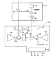
図1乃至図15は、光信号増幅3端子装置に関連する実際例を示すものであって、図1はその一実施例の光信号増幅3端子装置10を示している。
FIGS. 1 to 15 show actual examples related to an optical signal amplification three-terminal device, and FIG. 1 shows an optical signal amplification three-
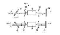
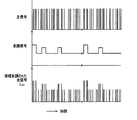
図1において、第1レーザ光源12は、たとえば1555nmの第1波長λ1の第1レーザ光(第1入力光)L1を出力し、第1光変調器14が設けられた光ファイバF1を介して伝播させる。第2レーザ光源16は、たとえば1548nmの第2波長λ2の第2レーザ光(第2入力光)L2を一定の強度で連続的に出し、第2光ファイバF2を介して伝播させる。上記第1レーザ光源12はたとえば可変波長半導体レーザが用いられるが、第2レーザ光源16はたとえば単一波長の半導体レーザが用いられる。上記第1光変調器14は、図示しない信号発生器からの電気信号或いは光信号に従って、たとえば図3の上段の波形に示すように、その電気信号或いは光信号の周波数のパルス信号となるように通過光である第1レーザ光L1を強度変調する。第1光カプラ18は、第1光入力手段として機能するものであり、上記光ファイバF1および光ファイバF2を光ファイバF3へ接続し、それら光ファイバF1および光ファイバF2を伝播してきた第1レーザ光L1および第2レーザ光L2を重畳(合波)し、第3光ファイバF3および第1光サーキュレータ20を介して第1光増幅素子26へ入力させる。
In FIG. 1, the first
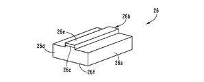
上記第1光増幅素子26は、たとえば図2に示す半導体光増幅素子(SOA:semiconductor optical amplifier)から構成される。
The first optical amplifying
図2において、化合物半導体たとえばインジウム燐(InP)やガリウム砒素(GaAs)から構成される半導体基板26aの上に形成された光導波路26bは、その半導体基板26aの上にエピタキシャル成長させられ且つホトリソグラフィーにより所定の導波路パターンに形成されたたとえばInGaAsP、GaInNAs、AlGaInPなどのIII−V族混晶半導体の多層膜であり、たとえばホトリソグラフィーを用いて所定幅のテープ状突起となるように形成されている。この光導波路26bは、半導体基板26aよりも屈折率が高い物質で構成されているので、光を厚み方向に閉じ込めつつ伝播させる機能を備えている。上記光導波路26b内の多層膜内には、pn接合により構成された活性層26c、キャップ層などが含まれ、その上には上部電極26eが固着されている。この活性層26cは、半導体基板26aの下面に固着された下面電極26fと上記上部電極26eとの間に電圧が印加され且つ上記pn接合に励起電流が流されることによって電子・正孔対が形成され、その活性層26cを通過する光が誘導放射作用によって増幅されるようになっている。上記活性層26cは、多重量子井戸、歪み超格子、或いは量子ドットから構成されている。多重量子井戸である場合は、たとえば、InP半導体基板26aからエピタキシャル成長させられることにより格子整合されたInGaAs(100Åの厚み)とInGaAsP(100Åの厚み)との6対により構成され、その活性層26cの上には、組成(屈折率)が段階的に変化させられたグリン(GRIN)構造のガイド層(2000Å)が順次設けられている。この活性層26cのデバイス長(光路長さ)は600μmであり、たとえば250mAの電流値によるエネルギ注入によって注入された電子が通過する光子による誘導放射によって価電子帯へ移動させられるときに光エネルギを放出して通過光を増幅させると考えられている。この250mAの電流値によるエネルギ注入により、たとえば波長1555nmにおいて20dB程度の利得が得られる。
In FIG. 2, an
前記第1光増幅素子26の1端面には、金属或いは誘電体がスパッタリングされることによって光を反射する処理が施された金属膜或いは誘電体多層膜などの反射手段26dが備えられているため、その1端面とは反対側に位置する他端面を通して光入力或いは光出力が行われるようになっている。したがって、前記第1レーザ光L1および第2レーザ光L2の合波光は、上記他端面を通して第1光増幅素子26内に入力されるとともに、上記反射手段26dに反射された光は再びその他端面を通して出力される。この第1光増幅素子26の活性層26c内では、上記第1レーザ光L1の入射によってその波長λ1を中心とする周囲波長の自然光が発生し、その自然光は第1レーザ光L1の強度変調に反比例して強度が増減する。この状態においてその自然光の波長範囲内にある第2波長λ2の第2レーザ光L2が通過させられると、その第2波長λ2は、その自然光と同様の変化を受けつつ増強させられる。すなわち、第1レーザ光L1の変調と同様ではあるが位相反転させられた変調を受けて増幅させられる。すなわち、第1光増幅素子26は、第2光増幅素子34とともにクロスゲイン変調特性すなわち相互利得変調特性を備えている。
Since one end face of the first optical amplifying
第1光サーキュレータ20は、第1光増幅素子26から出力された光を、第3光ファイバF3ではなく、第1波長選択素子28を備えた第4光ファイバF4へ導く。第1波長選択素子28は、前記第1光増幅素子26に接続され、その第1光増幅素子26から出力された光のうちから第2波長λ2である1548nmの光を抽出する。この第1波長選択素子28は、光フィルタ素子として機能するものであり、たとえば紫外線が局部的に照射されることにより、第4光ファイバF4の一部が長手方向において屈折率が周期的に変化させられたファイバーグレーティングフィルタであって、第2波長λ2を中心波長とし且つ半値幅が1nmの光を選択して透過させるものである。なお、第1波長選択素子28は、屈折率が異なる多数組の層が積層されて成る多層膜フィルタ、フォトニックバンドギャップを有するフォトニッククリスタルのいずれかから構成されてもよい。
The first
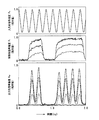
第2光カプラ30は、第2光入力手段として機能するものであり、上記第1波長選択素子28により第1光増幅素子26から出力された光のうちから選択された第2波長λ2の光と、たとえば図3の中段の波形に示す第3波長λ3の制御光である第3レーザ光L3とを重畳(合波)し、第5光ファイバF5および第2光サーキュレータ32を介して第1光増幅素子26と同様に構成された第2光増幅素子34へ入力させる。この第2光増幅素子34では、変調された第2波長λ2は、その第2波長λ2を中心とする自然光の波長範囲内の第3波長λ3の制御光によってさらに変調を受け、第3波長λ3に関しては、図3の下段に示す波形とされる。第2光サーキュレータ32は、第2光増幅素子34から出力された光を、第5光ファイバF5へではなく、第2光フィルタ素子36を備えた第6光ファイバF6へ導く。上記第2光フィルタ素子36は、第2光増幅素子34から出力された光のうちから第3波長λ3の光を選択し、図3の下段に示す出力光L4として出力する。図3において、中段の波形に示す制御光L3の実線、1点鎖線、破線は、下段に示す出力光L4の実線、1点鎖線、破線に対応しており、出力光L4は制御光L3に対して約30倍のゲイン(増幅率)を有している。
The second
図4および図5は、上記のようにして構成された光信号増幅3端子装置10の相互利得変調型波長変換作用の特性を示している。図4は、第1入力光である第1レーザ光L1の信号強度PINを示す横軸と出力光である第4レーザ光L4の信号強度POUTを示す縦軸とからなる二次元座標において、制御光L3の信号強度PCをパラメータとする第4レーザ光L4の入出力特性図である。図から明らかなように、トランジスタなどのような3端子増幅素子と同様に、出力光である第4レーザ光L4の信号強度POUTは、制御光L3の信号強度PCの変化に応答し、且つその変化が増幅されて変調させられるとともに、第1入力光である第1レーザ光L1の信号強度PINの変化に応答し、且つその変化が増幅されて変調させられる。また、図5は、第1入力光である第1レーザ光L1の周波数を示す横軸と出力光である第4レーザ光L4の信号変調度H(%)を示す縦軸とからなる二次元座標において、その第4レーザ光L4の周波数特性を示している。図5によれば、5GHzまでは信号変調度Hの低下が見られなかった。上記信号変調度Hはたとえば次式(1)により表される。但し、Imaxは光信号の最大値、Iminは光信号の最小値である。なお、前記活性層26cに量子ドットが用いられる場合には、100GHz以上の範囲において信号変調度Hの低下が見られない。
4 and 5 show the characteristics of the mutual gain modulation type wavelength conversion action of the optical signal amplification three-
H=100×(Imax−Imin)/(Imax+Imin)・・・(1) H = 100 × (I max −I min ) / (I max + I min ) (1)
なお、本発明者の実験によれば、上記制御光L3を第3波長λ3から第1波長λ1へ変更することにより、第1波長λ1の出力光L4が得られるとともに、上記と同様の光信号増幅効果結果が得られた。また、上記においては、第2レーザ光L2の第2波長λ2は第1レーザ光L1よりも短波長であったが、その第2レーザ光L2の第2波長λ2を第1レーザ光L1よりも長波長としても上記と同様の光信号増幅効果結果が得られただけでなく、たとえば図3の下段の波形の最低値が零に近づくというような、出力光L4の基線が第1レーザ光L1と同様に零に近接するという更なる効果が認められた。また、第1波長λ1の第1入力光L1を第2波長λ2の第2レーザ光L2と同様に連続光(バイアス光)として、第3波長λ3の第3入力光L3に信号変調をかけると、第3波長λ3の出力光L4は、その第3入力光L3の信号が10以上の増幅率で増幅されたものとして出力された。 According to the experiment by the present inventor, by changing the control light L 3 from the third wavelength λ 3 to the first wavelength λ 1 , the output light L 4 of the first wavelength λ 1 is obtained, and the above-mentioned The same optical signal amplification effect result was obtained. In the above description, the second wavelength λ 2 of the second laser light L 2 is shorter than the first laser light L 1 , but the second wavelength λ 2 of the second laser light L 2 is the first wavelength. not only may the same optical signal amplification effect results as long wavelength is obtained than the laser light L 1, for example, a minimum value of the lower waveform of Figure 3 is that that approaches zero, the output light L 4 baseline was observed further effect close to zero similarly to the first laser beam L 1. Further, as the first wavelength lambda 1 of the first input light L 1 of the second wavelength lambda 2 of the second laser beam L 2 in the same manner as in continuous light (bias light), the third input light L 3 of the third wavelength lambda 3 Was subjected to signal modulation, the output light L 4 of the third wavelength λ 3 was output as the signal of the third input light L 3 amplified with an amplification factor of 10 or more.
図6(a)は、上記光信号増幅3端子装置10が適用された2つの光NANDゲート40から構成されたフリップフロップ回路42を示し、図6(b)は2つの光NORゲート44から構成されたフリップフロップ回路46を示している。電子回路におけるNANDゲートおよびNORゲートはよく知られているように複数のトランジスタから構成されており、そのトランジスタに替えて上記光信号増幅3端子装置10が光回路中に設けられることにより光NANDゲート40およびNORゲート44が構成され、それら1対の光NANDゲート40および1対の光NORゲート44からフリップフロップ回路42および46が構成される。このフリップフロップ回路42および46によれば、光により情報が記憶される。
6A shows a flip-
図7は、前記光信号増幅3端子装置10が適用された光演算増幅器(光オペレーショナルアンプ)48を示している。電子回路における演算増幅器はよく知られているように複数のトランジスタから構成されており、そのトランジスタに替えて上記光信号増幅3端子装置10が光回路中に設けられることにより、光演算増幅器48が構成される。
FIG. 7 shows an optical operational amplifier (optical operational amplifier) 48 to which the optical signal amplification three-
以上のように構成された図1の光信号増幅3端子装置10においては、第1波長λ1の第1入力光L1と第2波長λ2の第2入力光L2とが入力された第1光増幅素子26からの光から選択された第2波長λ2の光と、第3波長λ3の第3入力光(制御光)L3とが第2光増幅素子34へ入力させられるとき、その第2光増幅素子34から出された光から選択された第3波長λ3の出力光L4は、前記第1波長λ1の第1入力光L1および/または第3波長λ3の第3入力光L3の強度変化に応答して変調された光であって、その第3波長λ3の第3入力光(制御光)L3に対する信号増幅率が2以上の大きさの増幅信号となるので、光信号の増幅処理を制御入力光を用いて直接行うことができる光信号増幅3端子装置10を得ることができる。
Or more in the optical
また、本実施例の光信号増幅3端子装置10によれば、前記第1波長λ1の第1入力光L1は変調光であり、前記第2波長λ2の第2入力光L2は連続光であり、前記第3波長λ3の第3入力光L3は制御光であり、前記第3波長λ3の出力光L4は、その制御光L3の入力区間においてその第1入力光L1の変調信号が増幅された信号波形を備えたものであることから、第3波長λ3の出力光L4は、制御光L3の入力区間において第1波長λ1の第1入力光L1の強度変化に応答して変調された増幅光となるので、増幅された光信号のスイッチング処理を制御入力光を用いて直接行うことができる光信号増幅3端子装置10を得ることができる。
Further, according to the optical
また、本実施例では、前記第1波長λ1と第3波長λ3とは、同じ波長とすることもできることから、光信号増幅3端子装置10の信号入力光としての第1入力光L1及び第3入力光L3と、出力光L4とが同じ波長となるので、共通の波長で複数の光信号増幅3端子装置10を接続することが可能となり、複数個の光信号増幅3端子装置10を用いて集積度の高い光回路を構成することができる。
In the present embodiment, the first wavelength λ 1 and the third wavelength λ 3 can be the same wavelength. Therefore, the first input light L 1 as the signal input light of the optical signal amplification three-
また、本実施例では、前記第2波長λ2は、前記第1波長λ1よりも長波長とすることができるので、このような場合には、変調された第1入力光L1の増幅光である出力光L3が示す波形が、その第1入力光の波形の基線と同様に零レベルに近い基線となる利点がある。すなわち、変調度を大きくする利点がある。 In the present embodiment, the second wavelength λ 2 can be longer than the first wavelength λ 1. In such a case, amplification of the modulated first input light L 1 is performed. waveform indicated by the output light L 3 is light, there is an advantage that the base line close to the baseline as well as the zero level of the first input light waveform. That is, there is an advantage of increasing the modulation degree.
また、本実施例では、第3波長λ3の出力光L4の第3波長λ3の制御光L3に対する信号増幅率は、10以上の値であるので、光信号増幅3端子装置の増幅機能が一層高められ、その応用範囲が拡大される。 Further, in this embodiment, the third signal gain for the control light L 3 of the wavelength lambda 3 of the third wavelength lambda 3 of the output light L 4 are, because it is 10 or more values, the amplification of the optical signal amplifying triode unit The function is further enhanced and the application range is expanded.
また、本実施例では、第1光増幅素子26および第2光増幅素子34は、pn接合から構成される活性層26cを備えた半導体光増幅素子であることから、信号増幅率および応答速度が一層高められた光信号増幅3端子装置10が得られる。
In the present embodiment, the first optical amplifying
また、本実施例では、第1光増幅素子26および第2光増幅素子34の活性層26cは、量子井戸または量子ドットから構成されたものであることから、一層高い信号増幅率および速い応答速度を備えた光信号増幅3端子装置10が得られる。特に量子ドットを用いた場合には100GHz以上の応答速度が得られる。また、活性層として歪み超格子を用いると偏波依存性が小さくなる。
In this embodiment, the
また、本実施例では、第1光増幅素子26および第2光増幅素子34は、活性層26cを通過した光を反射するために金属蒸着などにより形成されたミラーなどの反射手段26dをその一端面に備え、他端面を通して入力光が入力され且つ出力光が取り出されるものであることから、1端面に備えられたミラーなどの反射手段26dによって活性層26cにおける通過パスが実質的に長くされるので、信号増幅率が一層高められる。また、フィードバック効果によって一層変調度が高められる。
In the present embodiment, the first optical amplifying
また、本実施例では、第1光増幅素子26および第2光増幅素子34の他端面を通してその中に入力光を入力させ、その他端面を通して出力される光をその入力光とは異なる光路へ導く光サーキュレータ20および32が設けられていることから、第1光増幅素子26および第2光増幅素子34の他端面から出た光はその他端面へ入力させる光を導く導波路に入ることがなく、専ら他の出力用導波路に導かれる。
Further, in this embodiment, input light is input into the first optical amplifying
また、本実施例では、第1波長選択素子28および/または第2波長選択素子36は、導波路または光ファイバ内の光伝播方向において屈折率が周期的に変化させられたグレーティングフィルタ、屈折率が異なる多数組の層が積層されて成る多層膜フィルタ、フォトニックバンドギャップを有するフォトニッククリスタルのいずれかから構成されたものであることから、第1光増幅素子26或いは第2光増幅素子34からの光から第2波長λ2或いは第3波長λ3が好適に抽出される。
In the present embodiment, the first
また、前述の光信号増幅3端子装置10は、光NANDゲート40、その一対の光NANDゲート40から成る光フリップフロップ回路42、または光演算増幅器46を構成することができ、光集積回路の機能を高めることができる。
The optical signal amplification three-
また、本実施例の第1光増幅素子26において、第2波長λ2は第1波長λ1の第1入力光L1の周囲光の波長域内の波長であり、第2光増幅素子34において、第3波長λ3は、第2波長λ2の入力光の波長域内の波長であるので、第1光増幅素子26或いは第2増幅素子34からの出力光に含まれる第2波長λ2或いは第3波長λ3の信号が好適に増幅される。
In the first optical amplifying
また、第1光増幅素子26の一端面に設けられた反射手段26が、第1波長λ1の光は透過させるが第2波長λ2の光は反射する波長選択性反射膜から構成されている場合は、第1波長選択素子28が不要となる。第1光増幅素子26と同様に構成されている第2光増幅素子34の反射手段が、第2波長λ2の光は透過させるが第3波長λ3の光は反射する波長選択性反射膜(波長選択性ミラー)から構成されている場合は、第2波長選択素子36が不要となる。上記波長選択性反射膜は、たとえば屈折率が異なる誘電体層が交互に積層された誘電体多層膜から構成される。
The reflecting means 26 provided on one end face of the first optical amplifying
次に、他の実施例を説明する。なお、以下の説明において前述の実施例と共通する部分には同一の符号を付して説明を省略する。 Next, another embodiment will be described. In the following description, parts common to those in the above-described embodiment are denoted by the same reference numerals and description thereof is omitted.
図8は、前述の光信号増幅3端子装置10の他の実施例の光信号増幅3端子装置50の構成例の要部を示している。本実施例の波長変換装置50は、第1光入力手段として機能するハーフミラー51および集光レンズ52を通して光信号LAが第1光増幅素子26の一方の端面に入力され、その第1光増幅素子26の他方の端面から集光レンズ53を通して出力された光のうち第1波長λ1の光は透過させられるが、バイアス光L2の波長λbの光は第1波長選択素子として機能する波長選択型ミラー54により反射されて第1光増幅素子26に戻される。その第1光増幅素子26の一方の端面から出力された光は上記ハーフミラー51により反射されるとともに第2光入力手段として機能するハーフミラー55により制御光LCと合波され、集光レンズ56を通して第2光増幅素子34の一方の端面に入射される。この第2光増幅素子34の他方の端面から集光レンズ57を通して出力された光のうちのバイアス光L2の波長λbの光は透過させられるが、制御光LCと同じ波長成分は第2波長選択素子として機能する波長選択型ミラー58により反射されて第2光増幅素子34に戻される。その第2光増幅素子34の一方の端面から出された出力光L3は、前述の光信号増幅3端子装置10と同様のものとなる。このように構成された波長変換装置50によれば、前述の光信号増幅3端子装置10と同様の相互利得変調型の波長変換作用および光増幅作用が得られる。上記波長選択型ミラー58および波長選択型ミラー54は、集光レンズ57および集光レンズ53を通して第2光増幅素子34の端面および第1光増幅素子26の端面と光学的に結合されている。上記集光レンズ52、53、56、57はたとえばマイクロレンズにより構成され、上記光信号LAや出力光L3などは光ファイバにより伝送される。なお、ハーフミラー51および55は光カプラ又は光サーキュレータにより置き替えられてもよい。
FIG. 8 shows a main part of a configuration example of an optical signal amplification three-
図9は、前記光信号増幅3端子装置10の他の実施例の光信号増幅3端子装置59の構成例の要部を示している。本実施例の光信号増幅3端子装置59は、直列に配設された第1光増幅素子26および第2光増幅素子34と、光信号LAおよびバイアス光Lb(波長λb)を第1光増幅素子26の内側端面に入射させる光カプラ60および61と、第1光増幅素子26の外側端面からの光のうち第1波長λ1の光は透過させるが波長λbの成分を反射して第1光増幅素子26内に戻す波長選択性の反射器62と、その第1光増幅素子26の内側端面から出射した光のうち波長λbの成分を通過させて第2光増幅素子34の内側端面に入射させるフィルタ63と、その第2光増幅素子34の外側端面に制御光LCを入射させる光カプラ64と、その第2光増幅素子34の外側端面から出射した光のうち制御光LCと同じ波長成分の光を透過させ、出力光L3として出力させるフィルタ65とを備えている。上記光カプラ60および61は第1光入力手段として機能し、上記光カプラ64が第2光入力手段として機能し、上記反射器62およびフィルタ65は第1波長選択素子および第2波長選択素子として機能している。このように構成された波長変換装置59によれば、前述の光信号増幅3端子装置10と同様の相互利得変調型の波長変換作用および光増幅作用が得られる。上記制御光LCの波長λCの光信号はフィルタ63で反射され且つフィルタ65を透過して出力される。波長λbの光成分はフィルタ65を透過しない。上記光カプラ60および61は、1個の光カプラから構成されてもよい。
FIG. 9 shows a main part of a configuration example of an optical signal amplification three-
図10は上記光信号増幅3端子装置59を、図2に示すモノリシック構造の第1光増幅素子26と同様のモノリシック構造すなわち1チップ構造で半導体基板26aの上に構成した例を示している。本実施例のモノリシック構造の光信号増幅3端子装置59では、第1光増幅素子26の外側位置、第1光増幅素子26と第2光増幅素子34との間の位置、第2光増幅素子34の外側位置には、屈折率が周期的に変化させられたグレーティングにより構成された反射器62、フィルタ63、フィルタ65が順次設けられている。なお、直線状の光導波路26bから分岐させられている一対の分岐導波路は、前記光カプラ60および61および光カプラ64に対応している。
FIG. 10 shows an example in which the optical signal amplification three-
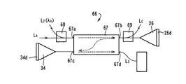
図11は、前述の光信号増幅3端子装置10の他の実施例の光信号増幅3端子装置66の構成例の要部を示している。本実施例の波長変換装置66は、一対の反射型の第1光増幅素子26および第2光増幅素子34と、その一対の反射型の第1光増幅素子26および第2光増幅素子34に接続された第2端子67bおよび第3端子67cを含む4端子を備え、その4端子間において光を伝送するが所定の端子からの出射光とその端子への入射光とが異なる光路とする4端子型光サーキュレータ67と、光信号LAおよびバイアス光Lb(波長λb)を合波して4端子型光サーキュレータ67の第1端子(第1ポート)67aに入射させる光カプラ68と、反射型第1光増幅素子36から4端子型光サーキュレータ67の第2ポート67bに向かう波長λbの光に制御光LCを合波して第2光増幅素子34に入射させる光カプラ69とを備え、4端子型光サーキュレータ67の第4ポート67dから制御光LCと同じ波長成分の光を透過させる。上記第1光増幅素子26の反射面には、第1波長λ1の光は透過させるが第2波長λbの光を選択的に反射する反射膜26dが設けられており、上記第2光増幅素子34の端面には、第2波長λbの光は透過させるが制御光LCと同じ波長λC成分の光を反射する反射膜34dが設けられている。このように構成された光信号増幅3端子装置66によれば、前述の光信号増幅3端子装置10と同様の相互利得変調型の波長変換作用および光増幅作用が得られるとともに、4端子型光サーキュレータ67を通されるために出力光L3の変調度が高められる。本実施例の光信号増幅3端子装置66は図1の光信号増幅3端子装置10に比較して構成が簡単となる利点がある。なお、上記光カプラ69は、4端子型光サーキュレータ67の第3ポート67cから第2光増幅素子34に向かう波長λbの光に制御光LCを合波して第2光増幅素子34に入射させるものであってもよい。本実施例では、光カプラ68および光カプラ69が第1光入力手段および第2光入力手段として機能し、反射膜26dおよび34dが第1波長選択素子および第2波長選択素子として機能している。
FIG. 11 shows a main part of a configuration example of the optical signal amplification three-
図12は、上記光信号増幅3端子装置66がモノリシック構造とされた場合の例が示されている。このモノリシック構造の光信号増幅3端子装置66も、前述の図6、図10に示すものと同様に、半導体基板26aの上に形成された光導波路26bを備えている。この光導波路26bは、4端子型光サーキュレータ67と同様の機能を出すためのZ字状の部分と、光カプラ68および69としての機能を出すためにその一部から分岐させられた分岐導波路とが設けられている。上記光導波路26bのZ字状の部分のうちの屈折点には、一対の反射型第1光増幅素子26および第2光増幅素子34が前述の図2、図10に示すものと同様に構成されている。なお、反射膜26dおよび34dは、それら反射型第1光増幅素子26および第2光増幅素子34の外端面に設けられている。
FIG. 12 shows an example in which the optical signal amplification three-
図13は、前述の光信号増幅3端子装置10の他の実施例の光信号増幅3端子装置70の構成例の要部を示している。本実施例の光信号増幅3端子装置70は、たとえばGaAs等の矩形半導体基板71上に成長させられたたとえばGaInNAsなどのpn接合層(活性層)を有する混晶半導体層がホトリソグラフィーによりV字状に形成された第1光導波路72および第2光導波路73と、それら第1光導波路72および第2光導波路73に図示しない電極が設けられることによって設けられた第1光増幅素子26、第2光増幅素子34と、上記矩形半導体基板71の一端面であって上記第1光導波路72および第2光導波路73の交差部に設けられ、バイアス光Lbの第2波長λbの光および制御光LCは第2光導波路73へ向かって反射するが光信号LA第1波長λ1の光を選択的に透過させる波長選択性反射膜74と、矩形半導体基板71の一端面であって上記第2光導波路73の出力側に設けられ、第2波長λbの光は反射するが制御光LCと同じ波長成分の光を透過させる波長選択性反射膜75とを備えている。光信号LAとバイアス光Lbは光カプラ76によって合波されてから光導波路72の端面に入射され、制御光LCは、上記波長選択性反射膜75の外側に設けられた光カプラ77から第2光導波路156内に入射されるようになっている。このように構成された光信号増幅3端子装置70によれば、前述の光信号増幅3端子装置10と同様の相互利得変調型の波長変換作用および光増幅作用が得られる。また、本実施例の光信号増幅3端子装置70は、たとえばGaAs等の矩形半導体基板上に成長させられたGaInNAsなどのIII−V族混結晶半導体層から成るpn接合層(活性層)を有する混晶半導体層がホトリソグラフィーによって処理され且つ電極が付与されることによって1チップ化されるので、極小のサイズに構成される利点がある。本実施例では、上記光カプラ76および77が第1および第2光入力手段として機能し、上記波長選択性反射膜74および波長選択性反射膜75が第1波長選択素子および第2波長選択素子として機能している。
FIG. 13 shows a main part of a configuration example of an optical signal amplification three-
図14は、前述の光信号増幅3端子装置10の他の実施例の光信号増幅3端子装置78の構成例の要部を示している。本実施例の光信号増幅3端子装置78は、合波素子として用いられる光カプラ79、光分波素子として用いられる光カプラ80、および集光レンズ52を通して光信号LAが第1光増幅素子26の一方の端面に入力され、その第1光増幅素子26の他方の端面から集光レンズ53を通して出力された光のうち上記光信号LAの波長λ1は波長選択性フィルタ81により透過させられない(吸収される)がバイアス光の波長λbの光はそのフィルタ81を透過し且つ全反射型ミラー82により反射されて第1光増幅素子26に戻される。その第1光増幅素子26の一方の端面から出力された光は上記光カプラ80から他の光カプラ83へ伝送され、そこで制御光LCと合波される。次いで、光カプラ84および集光レンズ56を通して第2光増幅素子34の一方の端面に入射される。この第2光増幅素子34の他方の端面から集光レンズ57を通して出力された光のうちバイアス光の波長λbの光は波長選択性フィルタ85により透過させられない(吸収される)が制御光LCと同じ波長λCの成分はその波長選択性フィルタ85を透過し且つ全反射型ミラー86により反射されて第2光増幅素子34に戻される。その第2光増幅素子34の一方の端面から出された出力光L3は、光カプラ84によって外部たとえば後述の光分配装置150へ出力される。このように構成された光信号増幅3端子装置78によれば、前述の光信号増幅3端子装置10と同様の相互利得変調型の波長変換作用および光増幅作用が得られるだけでなく、光信号LAの波長λ1は波長選択性フィルタ81により吸収されて透過させられないことにより第1光増幅素子26側へ戻される割合が極めて少なくなり、特性が一層改善される利点がある。本実施例では、光カプラ79および光カプラ84が第1光入力手段および第2光入力手段として機能し、上記波長選択性フィルタ81および波長選択性フィルタ85が第1波長選択素子および第2波長選択素子として機能している。
FIG. 14 shows a main part of a configuration example of an optical signal amplification three-
図15は、前述の光信号増幅3端子装置10の他の実施例であって、1チップに複数個(本実施例では2個)の光信号増幅3端子装置88が集積化されたモノリシック構造の構成例の要部を示している。本実施例の複数組の光信号増幅3端子装置88は、たとえばGaAs等の矩形半導体基板89上に成長させられたたとえばGaInNAsなどのpn接合層(活性層)を有する混晶半導体層がホトリソグラフィーにより一方の端面から他方の端面にわたって直線状に形成され、互いに隣接する1対でV字状を成す第1光導波路90、第2光導波路91、および第3光導波路92と、それら第1光導波路90、第2光導波路91、および第3光導波路92に図示しない電極が設けられることによって設けられた第1光増幅素子26、第2光増幅素子34、および第3光増幅素子93と、上記矩形半導体基板89の一端面であって上記第1光導波路90および第2光導波路91の交差部と上記第3光導波路92の出力側端面とにわたって設けられ、バイアス光Lbの第2波長λbの光および制御光LCは第2光導波路91へ向かって反射するが光信号LAの第1波長λ1の光および制御光LCを選択的に透過させる波長選択性反射膜(波長選択性ミラー)94と、矩形半導体基板89の一端面であって上記第2光導波路91の出力側端面に設けられ、第2波長λbの光は透過するが制御光LCと同じ波長成分の光を第3光導波路92へ向かって反射する波長選択性反射膜(波長選択性ミラー)95とを、それぞれ備えている。光信号LAとバイアス光Lbは光カプラ96によって合波されてから第1光導波路90の入力側の端面に入射され、制御光LCは、上記波長選択性反射膜94の外側から第2光導波路91内に入射されるようになっている。このように構成された光信号増幅3端子装置88によれば、前述の光信号増幅3端子装置10と同様の相互利得変調型の波長変換作用および光増幅作用が得られる。本実施例の光信号増幅3端子装置88は、たとえばGaAs等の矩形半導体基板上に成長させられたGaInNAsなどのIII−V族混結晶半導体層から成るpn接合層(活性層)を有する混晶半導体層がホトリソグラフィーによって処理され且つ電極が付与されることによって1チップ化されるので、たとえば1.3μm波長帯の光信号の信号処理が可能な光信号増幅3端子装置10が極小のサイズに構成される利点がある。また、本実施例によれば、サーキュレータが不要となるとともに、3つの光増幅素子26、34、93により高出力が得られる。本実施例では、光カプラ96が第1光入力手段として機能し、波長選択性反射膜94が第2光入力手段および第1波長選択素子として機能し、波長選択性反射膜95が第2波長選択素子として機能している。
FIG. 15 shows another embodiment of the above-described optical signal amplification three-
図16乃至図33は、光信号転送方法、その光信号転送方法を好適に実施するための光信号ルータすなわち光信号中継(転送)装置に関連する実施例を示すものであって、これらによれば、所定の伝送路を介して伝送された一連の光信号を、複数の伝送路のうちのその光信号に含まれる行先情報に対応する伝送路へ転送することにより、高度情報処理のための光通信が可能とされる。 FIG. 16 to FIG. 33 show an embodiment related to an optical signal transfer method and an optical signal router, that is, an optical signal relay (transfer) device for favorably implementing the optical signal transfer method. For example, by transferring a series of optical signals transmitted through a predetermined transmission path to a transmission path corresponding to the destination information included in the optical signal among a plurality of transmission paths, Optical communication is possible.
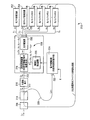
図16は、一方の光ネットワークにおける複数本の伝送路である入力光ファイバFA1乃至FAMと他方の光ネットワークにおける複数本の伝送路である出力光ファイバFB1乃至FBMとの間に配設されて、入力光ファイバFA1乃至FAMのいずれかを介して伝送された波長多重の光信号(レーザ光)LA1乃至LAMを、その光信号に振幅変調により付与されている行先情報に基づいて決定された出力光ファイバFB1乃至FBMのいずれか内の波長バスの1つへ転送するための光信号中継(転送)装置110を概略示す図である。この光信号中継装置110は光信号ルータとも称される。
FIG. 16 shows an arrangement between input optical fibers F A1 to F AM that are a plurality of transmission paths in one optical network and output optical fibers F B1 to F BM that are a plurality of transmission paths in the other optical network. Destination information in which wavelength multiplexed optical signals (laser light) L A1 to L AM transmitted through any of the input optical fibers F A1 to F AM are given to the optical signal by amplitude modulation. 2 is a diagram schematically showing an optical signal relay (transfer)
図16において、上記入力光ファイバFA1乃至FAMのいずれかにより伝送される光信号LA1乃至LAMはそれぞれ波長分割多重(WDM)信号であり、予め設定された複数種類の波長の光信号が重畳されている。したがって、たとえば光信号LA1に含まれる所定波長の一連の波長λ1の光信号LA11は、たとえばそのラベル部或いはタグ部において振幅変調が付与されることにより設けられた行先情報に従って、出力光ファイバFB1乃至FBMのいずれか1つの光ファイバFB内のいずれかの波長バスへ、すなわち予め設定された複数種類すなわちN種類の波長λ1乃至λNのいずれかの波長で転送される。出力光ファイバFB1乃至FBMにより、波長多重の光信号(レーザ光)LB1乃至LBMがそれぞれ伝送される。 In FIG. 16, optical signals L A1 to L AM transmitted by any one of the input optical fibers F A1 to F AM are wavelength division multiplexed (WDM) signals, and optical signals having a plurality of preset wavelengths. Are superimposed. Therefore, for example, a series of optical signals L A11 having a predetermined wavelength λ 1 included in the optical signal L A1 is output in accordance with destination information provided by, for example, applying amplitude modulation in the label portion or tag portion. Transferred to any wavelength bus in any one of the optical fibers F B of the fibers F B1 to F BM , that is, a plurality of preset wavelengths, that is, N types of wavelengths λ 1 to λ N . Wavelength multiplexed optical signals (laser lights) L B1 to L BM are transmitted by the output optical fibers F B1 to F BM , respectively.
上記光信号中継装置110は、所定数すなわちM本の入力光ファイバFA1乃至FAMから伝送された波長多重の光信号LA1乃至LAMをN種類の波長λ1乃至λN毎の一連の光信号(パケット)を波長毎の信号にそれぞれ分離、たとえば光信号LA1についてはそれをLA11乃至LA1Nにそれぞれ分離するM個の光分波器(AWG:Arrayed Waveguide Grating)S1乃至SMと、波長λ1乃至λN毎の一連の光信号(パケット)LA11乃至LA1Nをそれらに振幅変調により付与されている行先情報に従って波長変換するとともに従来の行先情報或いは新たな行先情報を振幅変調により付与する互いに同様に構成されたM個の第1中継器R1乃至第M中継器RMと、それら第1中継部R1乃至第M中継器RMから出力される光信号を合波して出力光ファイバFB1乃至FBMへ導くためのM個の合波器(AWG)T1乃至TMとを備えている。
The
図17は、上記互いに同様に構成された第1中継器R1乃至第M中継器RMの構成を説明するために、たとえば入力光ファイバFA1と出力光ファイバFB1との間に対応する位置に設けられた第1中継器R1を代表させてその構成を説明する図である。図17において、第1中継器R1には、入力光ファイバFA1から伝送された波長多重の光信号LA1から光分波器S1によってN種類の波長λ1乃至λN毎に分離されたの一連の光信号(パケット)LA11乃至LA1Nが光ファイバFA11乃至FA1Nを介して入力されると、その光信号LA11乃至LA1Nのラベル部或いはタグ部において振幅変調が付与されることにより設けられている行先情報に従って波長変換し且つそれまでと同じ行先情報か或いは新たな行先情報を示す振幅変調を施して出力するN個の互いに同様に構成された第1中継器本体部RB11乃至RB1Nが設けられている。第1中継器本体部RB11・・・第M中継器本体部RB1Nからそれぞれ出力されたN種類の波長λ1乃至λNのいずれかの波長の出力信号は、その波長および行先情報に従って分岐された光信号を伝送するためのN×M本のクロスコネクトファイバF111乃至F1NM・・・N×M本のクロスコネクトファイバFN11乃至FNNMをそれぞれ介して合波器T1乃至TMと接続されている。これにより、第1中継器本体部RB11・・・第M中継器本体部RB1Nの出力信号は、合波器T1乃至TMを介して出力光ファイバFB1乃至FBMのうちの所望の出力光ファイバへ所望の波長で伝送されるようになっている。他の中継器RMを構成する中継機本体部RBM1乃至RBMNも、同様に、N×M本のクロスコネクトファイバF111乃至FINM・・・N×M本のクロスコネクトファイバFN11乃至FNNMをそれぞれ介して合波器T1乃至TMと接続されている。なお、図17に示すように、同じ波長たとえば波長λ1の信号を伝送するクロスコネクトファイバF111、F211、・・・FN11の出力端が結合され、ファイバFB11を介して合波器T1に入力されている。波長λNの信号を伝送するクロスコネクトファイバF1N1、F2N1、・・・FNN1の出力端が結合され、ファイバFBN1を介して合波器T1に入力されている。 Figure 17 corresponds to between for explaining the structure of the first relay R 1 to M th relay R M, which is configured above each other Similarly, for example, the input optical fiber F A1 and the output optical fiber F B1 the first relay R 1, which is provided at a position as a representative is a diagram explaining the configuration. In FIG. 17, the first repeater R 1 is separated into N types of wavelengths λ 1 to λ N from the wavelength multiplexed optical signal L A1 transmitted from the input optical fiber F A1 by the optical demultiplexer S1. When a series of optical signals (packets) L A11 to L A1N are input through optical fibers F A11 to F A1N , amplitude modulation is applied to the label portion or tag portion of the optical signals L A11 to L A1N. N pieces of first repeater main bodies RB configured in the same manner as described above, which perform wavelength conversion in accordance with destination information provided and output the same destination information as before or amplitude modulation indicating new destination information. 11 to RB 1N are provided. 1st repeater body RB 11 ... Output signal of any one of N wavelengths λ 1 to λ N output from the Mth repeater body RB 1N is branched according to the wavelength and destination information. N × M cross-connect fibers F 111 to F 1NM for transmitting the transmitted optical signals, and N × M cross-connect fibers F N11 to F NNM , respectively, combiners T 1 to T M Connected with. Accordingly, the output signal of the first repeater body RB 11 ... M-th repeater body RB 1N is output from the output optical fibers F B1 to F BM through the multiplexers T 1 to T M. Is transmitted to the output optical fiber at a desired wavelength. Other repeaters R M to the relay device body portion RB M1 constituting the RB MN likewise, N × M present in the cross-connect fiber F 111 to F INM ··· N × M present cross-connect fiber F N11 to the It is connected to the multiplexers T 1 to T M via F NNM , respectively. As shown in FIG. 17, the output ends of the cross-connect fibers F 111 , F 211 ,... F N11 that transmit signals of the same wavelength, for example, the wavelength λ 1 are coupled, and the multiplexer is connected via the fiber F B11 . It is input to the T 1. Cross-connect fiber F 1N1, F 2N1 to transmit signals of wavelength lambda N, the output end of · · · F NN1 is coupled, is input to the multiplexer T 1 via the fiber F BN1.
上記光分波器S1は、たとえば、回折格子やプリズムなどの角度分散素子、誘電体多層膜の干渉フィルタなどの波長選択性反射/透過膜、或いは光導波路形分波回路などを利用して構成される光分波回路としてよく知られたものである。また、上記合波器T1は、たとえば、マイクロレンズを主要な構成要素とする光方向性結合回路、複数本の並列配置された光ファイバの一部が局部的に結合された分布結合形光多重カプラ、四角管の内壁における多重反射或いは平面板内における混合を利用した集中結合形光多重カプラなどから構成される。 The optical demultiplexer S 1 uses, for example, an angle dispersive element such as a diffraction grating or a prism, a wavelength selective reflection / transmission film such as a dielectric multilayer film interference filter, or an optical waveguide demultiplexing circuit. This is a well-known optical demultiplexing circuit. Further, the multiplexer T 1, for example, optical directional coupling circuit for a main constituent a microlens, a part of the parallel arranged optical fiber a plurality of the locally bound Coupled type optical It is composed of multiple couplers, concentrated coupling type optical multiple couplers utilizing multiple reflection on the inner wall of the square tube or mixing in a flat plate.
また、上記第1中継器本体部RB11は、たとえば図18に示すように構成される。図18において、光分波器S1から光ファイバFA11を介して入力された光信号LA11は、光分波合波器として機能する第1光カプラ114、光遅延素子116、および相互利得変調型の波長変換装置(光スイッチング装置、光信号増幅3端子装置本体)118が順次接続されている。上記第1光カプラ114は、光ファイバを主体とした分岐回路、マイクロレンズを主体とした分岐回路などから構成される。光ファイバを主体とした分岐回路では、たとえば一対の光ファイバの所定区間を相互に密着して並行した状態で或いは螺旋状に相互にひねった状態で相互に密着させたり、透過および反射可能な反射膜を光ファイバの分岐点に設けたりすることにより構成される。マイクロレンズを主体とした分岐回路では、たとえば集束性ロッドレンズで平行ビーム化された光をくさび型屈折面或いは反射面を用いて分岐させるように構成される。この第1光カプラ114は、双方向性すなわち可逆性を備えているので、反対向きに光信号が伝播させられるときには、光信号を合波して第1光ファイバ112内を反対向きに伝送させる合波器として機能する。
Further, the first repeater body RB 11 is configured as shown in FIG. 18, for example. 18, the optical signal L A11, which is input from the optical splitter S 1 via the optical fiber F A11, the first
また、光遅延素子116は、上記光ファイバFA11内を伝送される光信号を所定時間だけ遅延させるためのものであり、たとえば所定の長さの光ファイバを巻回して伝播距離を設けることよりその所定の伝播距離を伝播する伝播時間だけ遅延させるように構成される。この光遅延素子116の遅延時間は、波長変換装置118内において、そこで波長変換される光信号とその光信号の伝送先を示す制御光とが同期するように予め実験的に求められる。
The
上記第1光カプラ114により光ファイバFA11内の光信号から分岐された分岐光信号は、光ファイバ120とこれに接続された光電信号変換器122とを介して電子制御装置124へ供給される。電子制御装置124は、たとえばCPUがRAMの一時記憶機能を利用しつつROMに予め記憶されたプログラムに従って入力信号を処理する所謂マイクロコンピュータにより構成される。この電子制御装置124は、光ファイバ120を介して伝送された光信号に含まれている振幅変調で示されるコード信号すなわち行先情報に基づいて、その光信号をルーティングするためにその行先情報に対応する波長指令信号を制御光発生装置126へ供給する。たとえば、電子制御装置124は、光ファイバ120から入力される光信号LA11に含まれる振幅変調信号のみを抽出し、制御光発生装置126からその振幅変調で示される行先情報に対応する波長に応じた制御光LCを発生させるものであることから、アドレス信号以外の信号に対応する電磁波が信号処理によって発生しない。
The branched optical signal branched from the optical signal in the optical fiber F11 by the first
上記制御光発生装置126は、予め設定された複数種類の波長λCの制御光LCを出力する制御光源を有し、前記電子制御装置124からの指令信号、すなわち光信号L1に含まれる分岐情報に応じて選択された波長指令信号に従って、その分岐情報に対応する波長λCを有する制御光LCを前記波長変換装置118に対して供給する。制御光発生装置126は、転送先の出力光ファイバFB1乃至FBM内の波長バスの本数に対応する複数種類たとえばN種類の波長λC1、λC2、λC3、・・・λCNの制御光LCを択一的或いは選択的に発生させる。図19、図20、図21は、その制御光発生装置126の構成例をそれぞれ示している。
The
図19において、制御光発生装置126は、制御光源に対応する相互に波長が異なる単一波長の光を出力する複数のレーザ光源126L1乃至126Lnと、それらレーザ光源126L1乃至126Lnの出力側にそれぞれ設けられてそれらから出される出力光をそれぞれスイッチングするための複数(N個)の光変調器126M1乃至126Mnと、それら光変調器126M1乃至126Mnを通過した光を合波し、制御光として出力する単一の光合波器126Sとから構成され、電子制御装置124からの分岐指令信号に従ってレーザ光源126L1乃至126Lnおよび光変調器126M1乃至126Mnが作動させられることにより、光信号LA11に含まれる振幅変調信号が示す行先情報(分岐情報)に応じて選択された波長λCの制御光LCを出力する。上記複数のレーザ光源126L1乃至126Lnとしては、たとえば半導体レーザダイオードが用いられる。図20において、制御光発生装置126は、制御光源に対応する相互に波長が異なる単一波長の光を出力する複数のレーザ光源126L1乃至126Lnとそれらレーザ光源126L1乃至126Lnから出力された光を1つの導波路に合波する単一の光合波器126Sと、その光合波器126Sの出力側に設けられてそれから出される出力光をスイッチングしてブランキング区間を遮断する単一の光変調器126Mとから構成され、電子制御装置124からの分岐指令信号に従ってレーザ光源126L1乃至126Lnおよび光変調器126Mが作動させられることにより、光信号LA11に含まれる分岐情報に応じて選択された波長λCの制御光LC出力する。図21において、制御光発生装置126は、出力光の波長を変更することが可能な波長可変レーザ光源126LVと、その波長可変レーザ光源126LVの出力側に設けられてそれから出される出力光をスイッチングしてブランキング区間を遮断する単一の光変調器126Mとから構成され、電子制御装置124からの分岐指令信号に従って波長可変レーザ光源126LVおよび光変調器126Mが作動させられることにより、光信号L1に含まれる分岐情報に応じて選択された波長λCの制御光LCを出力する。上記波長可変レーザ光源126LVは、たとえば分布ブラッグ反射型レーザ、マイクロマシン面発光レーザ、温度同調DFBレーザなどが用いられる。分布ブラッグ反射型レーザでは、その光共振器を構成する一対のミラーのうちの一方を構成するDBR層(ブラッグ反射層)に電流を注入し、プラズマ効果によってその部分の屈折率を変化させることにより光共振波長が可変とされる。マイクロマシン面発光レーザでは、マイクロマシンによって光共振器長が変化されることにより光共振波長が可変とされる。温度同調DFBレーザでは、温度による屈折率変化により光共振波長が可変とされる。なお、上記光変調器126M1乃至126Mn、126Mは、たとえば駆動電流または駆動電圧がpn接合部に加えられることによって透過光をオンオフさせる半導体型光変調器や、ニオブ酸リチウムなど単結晶のような電気光学効果を有する物質に外部から駆動電圧を印加することにより透過光をオンオフさせる外部変調型光変調器などから構成される。
In FIG. 19, the
上記図18の前記光波長変換装置118は、第2波長選択素子としても機能する光分配装置150と共に光信号増幅3端子装置128を構成するものであり、基本的には図1、図8乃至図15に示す光信号増幅3端子装置10、50、59、66、70、78、88のいずれかと同様に構成される。本実施例の光波長変換装置118は、たとえば図22に示されるように、第1光ファイバ112を介して入力された光をクロスゲイン変調特性を利用して増幅および波長変換して出力する複数個の光増幅素子に対応する一対の第1光増幅素子136および第2光増幅素子144を直列に備え、上記第1光ファイバ112を介して入力された光信号を増幅するとともに、その光信号に含まれる分岐情報に対応する制御光LCの入力に同期してその制御光LCと同じの波長の光L3を出力するように構成されている。すなわち、図22において、レーザ光源130は、たとえば単一波長の半導体レーザから構成され、光信号L1(第1入力光)の波長λ1たとえば1555nmよりも長い波長λ2たとえば1565nmのレーザ光(第2入力光)L2を一定の強度で連続的に出力する。第3光カプラ132は、第1光入力手段として機能するものであり、振幅変調されて第1光ファイバ112内を伝送された上記光信号L1と連続光である上記レーザ光L2とを重畳(合波)し、第1光サーキュレータ34を介して第1光増幅素子136へ入力させる。
The optical
上記第1光増幅素子136および第2光増幅素子144も、図2に示す第1光増幅素子26と同様に、半導体光増幅素子(SOA)から構成される。上記第1光増幅素子136は、スパッタリングなどによって光を反射する端面処理が施された鏡などの反射手段136dをその1端面に備えているため、その1端面とは反対側に位置する他端面を通して光入力或いは光出力が行われるようになっている。したがって、光信号L1(第1入力光)およびそれよりも長い波長λ2のレーザ光(第2入力光)L2の合波光は、上記他端面を通して第1光増幅素子136内に入力されるとともに、上記反射手段136dに反射された光は再びその他端面を通して出力される。この第1光増幅素子136の活性層内では、図2に示す第1光増幅素子26と同様に、光信号L1の変調と同様ではあるが位相反転させられた変調を受けて増幅され、第1光増幅素子136から出力される。すなわち、第1光増幅素子136は、第2光増幅素子144とともにクロスゲイン変調特性すなわち相互利得変調特性を備えている。
Similarly to the first optical amplifying
図22において、第1光サーキュレータ134は、上記第1光増幅素子136から出力された光を、第3光カプラ132へではなく、第1波長選択素子138へ導く。第1波長選択素子138は、前記第1光増幅素子136から出力された光のうちから第2波長λ2である1565nmの光を抽出する。この第1波長選択素子138は、光フィルタ素子として機能するものであり、たとえば紫外線が局部的に照射されることにより、光ファイバの一部が長手方向において屈折率が周期的に変化させられたファイバーグレーティングフィルタから構成されるものであって、第2波長λ2を中心波長とし且つ半値幅がたとえば1乃至十数nmの光を選択して透過させるものである。なお、第1波長選択素子138は、屈折率が異なる多数組の層が積層されて成る多層膜フィルタ、フォトニックバンドギャップを有するフォトニッククリスタルのいずれかから構成されてもよい。
In FIG. 22, the first
第4光カプラ140は、第2光入力手段として機能するものであり、上記第1波長選択素子138により第1光増幅素子136から出力された光のうちから選択された第2波長λ2の光と、第3波長λ3のレーザ光である制御光LCとを重畳(合波)し、第2光サーキュレータ142を介して第1光増幅素子136と同様に構成された第2光増幅素子144へ入力させる。第1光増幅素子136において変調された第2波長λ2は、この第2光増幅素子144において、その第2波長λ2を中心とする自然光の波長範囲内の第3波長λ3の制御光LCによってさらに変調を受け且つ増幅され、波長λ2の光と制御光LCの波長とされた変調光(出力光信号)L3との混合光が出力される。第2光サーキュレータ142は、第2光増幅素子144から出力された上記混合光(波長λ2の光および変調光L3)を、第4光カプラ140へではなく、光分配装置150へ出力させる。
The fourth
上記第2光増幅素子144から出力された光に含まれる変調光L3は、制御光LCの波長と同じ第3波長λ3の光であるので、制御光LCの波長がたとえばλC1、λC2、λC3、・・・λCNに変化させられると、第2光増幅素子144からの光L3の波長もたとえばλC1、λC2、λC3、・・・λCNに変化させられる。図23は、実験的に、上記光信号L1(第1入力光)をその上段に示す波形とし、制御光LCをその中段に示す波形としてそれぞれ入力させたときの光分配装置150の出力光L4の波形を示している。制御光LCの強度変化は、下段に示す光分配装置150の出力光L4の振幅変調に対応しており、その光分配装置150の出力光L4は制御光LCに対して約2倍乃至30倍のゲイン(増幅率)を有する。また、出力光L4の位相は上記光信号L1(第1入力光)と同じであり、位相反転されていない。
The modulated light L included in the output light from the second
図24は、上記のようにして構成されることにより光信号増幅3端子装置128として機能する波長変換装置118および光分配装置150において、第1光増幅素子136の活性層が量子ドットから構成された場合の特性を示している。図24において、第1入力光である信号光LA11の周波数を示す横軸と出力光である出力光L4の信号変調度H(%)を示す縦軸とからなる二次元座標において、その出力光L4の周波数特性が示されている。この図24によれば、100GHz程度までは信号変調度Hの低下がそれ程見られなかった。上記信号変調度Hはたとえば前式(1)により表される。
FIG. 24 shows that the active layer of the first optical amplifying
図18に戻って、上記波長変換装置118からの光のうちの変調光L3は、その波長すなわち制御光LCの波長λC(=λC1、λC2、・・・、λCn)毎に光分配装置150によって複数の導波路に対応するように予め定められたクロスコネクトファイバF111乃至F11M、F121乃至F12M、・・・F1N1乃至F1NMへそれぞれ選択的に分配される。また、波長変換装置118からの光のうちのそれらの波長λCと異なる波長λ2の光は分岐光ファイバFB0に分配される。この分岐光ファイバFB0の終端は後段に連結されておらず閉じられているので、波長λ2の光の伝播がここで阻止される。このように、光分配装置150は、第2光増幅素子144からの光から第3波長λCの出力光を選択する第2波長選択素子としても機能しているのである。
Returning to FIG. 18, the modulated light L 3 out of the light from the
上記光分配装置150において、たとえば、変調光L3が制御光LCの波長λCのうちの1つである単色光である場合にはクロスコネクトファイバF111乃至F11M、F121乃至F12M、・・・F1N1乃至F1NMのうちの1つの群へ択一的に分配されるが、2種類の混合色である場合にはクロスコネクトファイバF111乃至F11M、F121乃至F12M、・・・F1N1乃至F1NMのうちのいずれか2つの群へ分配される。上記光分配装置150は、たとえば図25に示すように、入力ポート150aに接続された第1スラブ導波路150bと、複数の出力ポート150cに接続された第2スラブ導波路150dと、それら第1スラブ導波路150bおよび第2スラブ導波路150dの間に設けられた長さの異なる複数のアレー導波路150eと、複数の出力ポート150cにそれぞれ接続されたクロスコネクトファイバF111乃至F11M、F121乃至F12M、・・・F1N1乃至F1NMとを備え、その入力ポート150aに入力された波長変換装置118からの変調L3(入力光)をその波長毎に複数の出力ポート150cのいずれかすなわちクロスコネクトファイバF111乃至F11M、F121乃至F12M、・・・F1N1乃至F1NMのいずれかへ分配するアレー導波路格子型光分波器から構成されている。なお、上記光分配装置150には、クロスコネクトファイバF111乃至F11M、F121乃至F12M、・・・F1N1乃至F1NMの端面に分岐光を集光させるための集光レンズなどの光学系が必要に応じて備えられる。本実施例では、前記制御光発生装置126、波長変換装置118、および光分配装置150が、光信号中継器本体部RB1の主要部を構成している。
In the
図26は、入力光ファイバFA1を介して伝送され且つ分波器S1により分離された波長λ1の光信号LA11の概念的構成を示す図であり、図27は、その信号光LA11の振幅変調が付与された波形、およびそれに振幅変調を付与する工程を説明する図である。図26において、光信号LA11は、たとえばパケットと称される一連の信号であって、その先頭部或いは先端部分には、パケットのタイトル、日付、文書名、頁番号などのヘッダー情報を付与するヘッダー部H、送信元や送信先のIPアドレス、ソースルーティングのようなルート情報、データリンク層のコネクション情報などなどの行先情報を示す信号を付与するラベル部(タグ部)LAが設けられている。光信号LA11は、図27に示すように、振幅変調が施されることによりヘッダー部Hやラベル部LAのうちの少なくとも上記行先情報が付与されている。この振幅変調は、たとえば図22に示す波長変換装置118や後述の図30に示すような振幅変調器を用いて、図27の上段部に示す主信号に第2段部に示す変調信号が重畳されることによって行われたものである。
FIG. 26 is a diagram showing a conceptual configuration of the optical signal L A11 having the wavelength λ 1 transmitted through the input optical fiber F A1 and separated by the branching filter S 1 , and FIG. It is a figure explaining the waveform to which the amplitude modulation | alteration of A11 was provided, and the process of providing an amplitude modulation to it. In FIG. 26, an optical signal L A11 is a series of signals referred to as packets, for example, and header information such as a packet title, date, document name, page number, etc. is added to the head or tip of the signal. header portion H, source or destination IP address, routing information, such as source routing, the label portion that applies a signal indicating the destination information such as such as connection information of the data link layer (tag portion) of L a is provided Yes. Optical signal L A11, as shown in FIG. 27, at least the destination information of the header portion H or label portion L A is given by the amplitude modulation is applied. For this amplitude modulation, for example, the
図28は、以上のように構成された本実施例の光中継器110の作動を、たとえば図18に示す第1中継器本体部RB11を代表させて説明するタイムチャートである。第1中継器本体部RB11において、図28の上段部に示す光信号LA11が光遅延素子116を介して波長変換装置118へ入力される(入力工程)一方で、第1光カプラ114によりその光信号LA11の一部が光電信号変換器122により電気信号に変換されて電子制御装置124へ供給され、その電子制御装置124により抽出された図28の第2段部に示す変調パルス信号(行先情報)が制御光発生装置126へ供給され、その制御光発生装置126からはその変調パルス信号が示す行先情報に従って決定された波長λCの制御光LCが図28の第3段部に示すように発生させられ、その発生に同期して波長変換装置118に入力されている光信号LA11が波長変換装置118において制御光LCの波長λCに変換され出力される(波長変換工程)。上記光遅延素子116により、光電信号変換器122による光電変換後の電子制御装置124の演算動作時間などに対応した時間だけ光信号LA11が遅延させられることにより上記の同期が行われる。たとえば光信号LA11に含まれる振幅変調パルスP1が示す行先情報が波長λ1の波長バスである場合は、波長λ1の制御光LCが発生されて光信号LA11が図28の下から2段目に示すように波長λ1に変換されて波長変換装置118から出力される。また、光信号LA11に含まれる振幅変調パルスP1が示す行先情報が波長λ2の波長バスである場合は、波長λ2の制御光LCが発生されて光信号LA11が図28の下段部に示すように波長λ2に変換されて波長変換装置118から出力され、光分配装置150によりその波長に従って分配される(光分配工程)。ここで、入力光である光信号LA11は第1光増幅素子136の出力が飽和する利得に設定されていることから、第1光増幅素子136から第1波長選択素子138を通して出力されて第2光増幅素子144へ入力される光信号は一定の大きさとされるので、その第2光増幅素子144から出力されて光分配装置150へ入力される波長変換後の光信号は振幅一定となるので、振幅変調が容易となる。本実施例の光中継器110の波長変換装置118では、入力光である光信号LA11の信号と出力光L3或いはL4の信号との間で位相反転がなく、その光信号LA11の波長は、第1光増幅素子136の利得範囲内であればどの波長が選択されてもよく自由度が高い利点がある。
FIG. 28 is a time chart for explaining the operation of the
図29は、前記光中継器110の他の作動すなわち波長変換と同時にラベリングして出力する作動を、たとえば図18に示す第1中継器本体部RB11を代表させて説明するタイムチャートである。第1中継器本体部RB11において、図29の上段部に示す光信号LA11が光遅延素子116を介して波長変換装置118へ入力される一方で、第1光カプラ114によりその光信号LA11の一部が光電信号変換器122により電気信号に変換されて電子制御装置124へ供給され、その電子制御装置124により抽出された図29の第2段部に示す変調パルス信号(行先情報)が制御光発生装置126へ供給される。制御光発生装置126では、その変調パルス信号が示す行先情報に従って決定された波長λCの制御光LCが発生させられて、その発生に同期して波長変換装置118に入力されている光信号LA11が制御光LCの波長λCに変換されて出力される。このときの変調パルス信号には、再付与するための行先情報が含まれているので、電子制御装置124はその行先情報を示すパルス信号を含むように図29の第3段部に示す振幅変調された制御光LCが発生させられる。たとえば光信号LA11に含まれる振幅変調パルスP1が示す行先情報が波長λ1の波長バスである場合は、波長λ1の制御光LCが発生されて光信号LA11が図29の下から2段目に示すように波長λ1に変換されて波長変換装置118から出力される。また、光信号LA11に含まれる振幅変調パルスP1が示す行先情報が波長λ2の波長バスである場合は、波長λ2の制御光LCが発生されて光信号LA11が図29の下段部に示すように波長λ2に変換されて波長変換装置118から出力される。
29, the operation to output the labeled concurrently with other operating i.e. wavelength conversion of the
上述のように、本実施例によれば、行先情報としてその一連の光信号LA11に振幅変調信号が付与され、その光信号LA11は振幅変調信号が示す行先へ転送される。このため、相互利得変調型の波長変換装置118に振幅変調された一連の光信号が入力される場合には、その光信号LA11の振幅変調が示す行先情報に対応した波長の制御光LCがその相互利得変調型の波長変換装置118に供給されると、その制御光LCと同じ波長の出力光が出力されるので、たとえば光分配装置150によりその出力光がその波長に応じた伝送路へ分配されることによってルーティングが行われるので、高速かつ小型のルーティング装置すなわち光信号転送装置或いは光信号中継装置110を構成することが可能となる。
As described above, according to the present embodiment, an amplitude modulation signal is given to the series of optical signals L A11 as the destination information, and the optical signal L A11 is transferred to the destination indicated by the amplitude modulation signal. Therefore, when a series of amplitude-modulated optical signals are input to the mutual gain modulation
また、本実施例によれば、上記一連の光信号LA11に付与された振幅変調は、90%以下の変調度で施されたものであるので、光信号LA11が損なわれず、且つ行先情報が光信号に確実に付与される。また、上記一連の光信号LA11パケット信号であり、前記行先情報はそのパケット信号の先頭部に設けられたラベル情報或いはタグ情報であるので、そのラベル部LA或いはタグ部において、振幅変調によりラベル情報或いはタグ情報が付与される。 In addition, according to the present embodiment, the amplitude modulation applied to the series of optical signals L A11 is performed with a modulation degree of 90% or less, so that the optical signal L A11 is not impaired and the destination information Is reliably added to the optical signal. Also, a series of the above optical signal L A11 packet signal, the so destination information is the label information or tag information provided at the head portion of the packet signal at its label portion L A or tag part, by the amplitude modulation Label information or tag information is given.
また、本実施例によれば、(a)行先情報として振幅変調が施された一連の光信号LA11を相互利得変調型の波長変換装置118へ入力させる入力工程と、(b)その光信号LA11とは異なり且つ振幅変調信号に対応する波長の制御光LCを上記相互利得変調型の波長変換装置118へ供給し、その相互利得変調型の波長変換装置118からその制御光LCの波長の光信号を出力させる波長変換工程と、(c)相互利得変調型の波長変換装置118から出力された光信号を光分配装置150に入力させ、その光信号をその波長に応じて光分配装置150に接続された複数の光伝送路へ分配する光分配工程とが、含まれるので、光信号LA11はその振幅変調信号が示す行先情報に応じた波長で光分配装置150に接続された複数の光伝送路へ分配される。
In addition, according to the present embodiment, (a) an input step for inputting a series of optical signals LA 11 subjected to amplitude modulation as destination information to the mutual gain modulation
また、本実施例によれば、上記波長変換工程は、相互利得変調型の波長変換装置118から出力される光信号LA11に制御光LCを用いて振幅変調を施すことにより、その光信号LA11に新たな行先情報を再付与するものであることから、信号光中継(転送)装置110内において適宜転送先を再付与できるので、たとえばリンクの状態、ノードの状態、ロタフィック状態に応じて転送ルートを決定する動的ルーティングが可能となる。
Further, according to the present embodiment, in the wavelength conversion step, the optical signal L A11 output from the mutual gain modulation
また、本実施例の光信号中継装置110によれば、行先情報として振幅変調信号が付与された一連の光信号LA11が伝送されて来ると、制御光発生装置126により、その一連の光信号LA11の振幅変調信号からその振幅変調信号が示す行先に対応し且つその光信号LA11とは異なる波長の制御光LCが発生させられ、相互利得変調型の波長変換装置118により、その一連の光信号LA11がその制御光LCの波長の光信号に変換され、光分配装置150により、その相互利得変調型波長変換装置118から出力された光信号がその波長に応じて複数の光伝送路へ分配されるので。高速かつ小型のルーティング装置すなわち光信号転送装置或いは光信号中継装置110が提供可能となる。
Also, according to the
また、本実施例では、光信号LA11に含まれる振幅変調信号に応じて、制御光発生装置126からその振幅変調信号が示す行先情報に応じた波長の制御光LCを発生させる電子制御装置124を備えたものであるので、波長変換機能とスイッチング機能を有する相互利得変調型波長変換装置118が行先情報に対応した波長の光信号を出力して光分配装置150による分配を可能とするので、高速かつ小型のルーティング装置すなわち光信号転送装置或いは光信号中継装置110が得られる。
Further, in this embodiment, in response to the amplitude modulation signals contained in the optical signal L A11, the electronic control device for generating control light L C of wavelengths corresponding to the destination information indicated by the amplitude modulation signal from the
また、本実施例では、(a)光ファイバ112内を伝播する光信号LA11を分岐させて電子制御装置124へ供給するための第1光カプラ(光分波器)114と、(b)その第1光カプラ114により分岐された光信号を電気信号に変換して電子制御装置124へ供給する光電信号変換器122と、(c)その光ファイバ112においてその第1光カプラ114よりも下流側に設けられ、その第1光ファイバ112から波長変換装置118に入力させる光信号L1を遅延させる光遅延素子116とが設けられ、上記電子制御装置124は上記光信号LA11に含まれる振幅変調信号を抽出して、その振幅変調信号が示す行先情報に対応する波長の制御光LCを制御光発生装置126から発生させるものであるので、波長変換機能とスイッチング機能を有する相互利得変調型波長変換装置118が行先情報に対応した波長の光信号を出力して光分配装置150による分配を可能とするので、高速かつ小型のルーティング装置すなわち光信号転送装置或いは光信号中継装置が可能となる。また、光信号LA11の一部が第1光カプラ114から分岐されて電子制御装置124へ供給される一方で、その光信号LA11の他の一部が光遅延素子116により遅延させられて波長変換装置118へ供給されるので、電子制御装置124における電子信号処理に用いられる遅れ時間にもかかわらず、制御光発生装置126から波長変換装置118へ供給される制御光LCがその波長変換装置118における光信号L1と好適に同期させられる。
In this embodiment, (a) a first optical coupler (optical demultiplexer) 114 for branching and supplying an optical signal LA 11 propagating in the
また、本実施例では、相互利得変調型の波長変換装置118は、(a)入力された光をクロスゲイン変調特性を利用して増幅および波長変換して出力するための第1光増幅素子136および第2光増幅素子144と、(b)光ファイバ112から入力された第1波長λ1の信号光LA11と、その信号光LA11とは異なる波長λ2の連続光であるレーザ光(第2入力光)L2とを合波して第1光増幅素子136に入力させる第3光カプラ(第1光合波器)132と、(c)第1光増幅素子136からの光から第2波長λ2の光を選択する第1波長選択素子138と、(d)その第1波長選択素子138により選択された第2波長λ2の光と第3波長λ3の制御光LCとを合波して第2光増幅素子144へ入力させる第4光カプラ(第2光合波器)140とを、含み、第3波長λ3の出力光L3は、制御光LCと同じ波長の光であって、第1波長λ1の信号光L1および/または第3波長λ3の制御光LCの強度変化に応答して変調されるものであることから、信号光L1とレーザ光(第2入力光)L2とが入力された第1光増幅素子136からの光から選択された第2波長λ2の光と制御光LCとが第2光増幅素子144へ入力させられるとき、その第2光増幅素子144から出された光から選択された第3波長λ3の変調光L3或いは出力光L4は、信号光L1および/または制御光LCの強度変化に応答して変調された光であって、制御光LCに対する信号増幅率が少なくとも2以上の大きさの増幅信号となるので、光信号L1の増幅処理を制御光LCを用いて直接行うことができる。
In the present embodiment, the mutual gain modulation type wavelength conversion device 118 (a) a first optical amplifying
また、本実施例では、光分配装置150は、入力ポート150aに接続された第1スラブ導波路150bと、複数の出力ポート150cに接続された第2スラブ導波路150dと、それら第1スラブ導波路150bおよび第2スラブ導波路150dの間に設けられた長さの異なる複数のアレー導波路50eと、複数の出力ポート50cに接続された分岐光ファイバFB1、FB2、FB3、・・・FBnとを備え、その入力ポート150aに入力された波長変換装置118からの出力光L3(入力光)をその波長毎に複数の出力ポート150cのいずれかすなわち分岐光ファイバFB1、FB2、FB3、・・・FBnのいずれかへ分配するように構成されているので、波長変換装置18から出力された制御光LCと同じ波長の変調光L3はその波長毎に複数の光ファイバFB1、FB2、FB3、・・・FBnのうちのいずれかへ選択的へ好適に分配される。
In this embodiment, the
また、本実施例の光信号中継装置110によれば、予め設定された複数種類の波長の制御光を出力する複数の単一波長のレーザ光源(制御光源)または波長可変レーザ光源を有し、前記光信号L1に含まれる分岐情報に応じて選択された波長の制御光LCを波長変換装置118に対して供給する制御光発生装置126が備えられているので、複数の分岐光導波路に対応する光ファイバFB1、FB2、FB3、・・・FBnのうちの上記制御光LCの波長に対して予め設定された所定の光ファイバへ光信号L1が選択的に分配される。
Further, according to the
また、本実施例の制御光発生装置126は、複数種類のレーザ光源126L1乃至26Lnまたは波長可変レーザ光源126LVから出力される制御光をスイッチングするための光変調器126Mを備えたものであるので、制御光発生装置126から出力された相互に異なる波長の制御光LCの立上がりおよび立下がりが急峻とされ、その応答性が高められる。
Further, the
また、本実施例では、第1光ファイバ112から入力される光信号L1に含まれる分岐情報に応じて、制御光発生装置126からその分岐情報に応じた波長を有する制御光LCを発生させる電子制御装置124を備えたものであるので、波長変換装置118から出力される変調光L3の波長がその光信号LA11に含まれる行先(分岐)情報に応じて切り換えられて、その波長毎に複数の光ファイバFB1、FB2、FB3、・・・FBnのうちのいずれかへ選択的に分配される。
Further, in the present embodiment, in accordance with the branching information contained in the optical signal L 1 input from the first
また、本実施例では、電子制御装置124は、光ファイバ112から入力される光信号LA11に含まれる行先情報(アドレス信号)のみを抽出し、前記制御光発生装置126からそのアドレス信号に対応する波長の制御光LCを発生させるものであることから、アドレス信号以外の信号に対応する電磁波が信号処理によって発生しないので、光信号L1の秘匿性が確保される利点がある。
In this embodiment, the
次に、他の実施例を説明する。なお、以下の説明において前述の実施例と共通する部分には同一の符号を付して説明を省略する。 Next, another embodiment will be described. In the following description, parts common to those in the above-described embodiment are denoted by the same reference numerals and description thereof is omitted.
図30は、前述の図18および図22に示す第1中継器本体部RB11が全光学的に構成された実施例を示している。図30において、波長変換装置118の第3光カプラ132に入力される入力光信号LA11の一部が光カプラ(光分波/合波素子或いは光合波器/光合波器)164によって分岐され、次いで、光カプラ166によって連続光である所定波長たとえば波長λ1乃至λNのいずれかの波長の連続光であるレーザ光Lと合波されて、図22に示す第1光増幅素子136と同様に構成されることによりクロスゲイン変調特性すなわち相互利得変調特性を備えた半導体光増幅素子(SOA)168に入力される。上記連続光であるレーザ光Lは、たとえば図19或いは図20に示すレーザ光源126L1乃至126Lnおよび光合波器126S、図21に示す可変レーザ光源126LVと同様に構成されたレーザ光源170が用いられる。この半導体光増幅素子168は、前記第1半導体光増幅素子136や第2半導体光増幅素子144に比較して相対的に応答速度が遅くなる特性となるように構成される。たとえば、前述のように、第1半導体光増幅素子136や第2半導体光増幅素子144が量子井戸または量子ドットから構成された活性層を備える場合には、上記半導体光増幅素子168はバルクから構成された活性層を備えるように構成される。この半導体光増幅素子168は、その利得および/または偏波状態が調整設定されることにより、高速のスイッチングに応答しないようにされている。これにより、図31の上段に示される入力光信号LA11が入力されると、その入力光信号LA11の振幅変調信号に対応する波形の制御光信号LC(図31の第2段目または第3段目)が上記半導体光増幅素子168から第4光カプラ(第2光合波器)140へ入力されるので、図31の下から2段目または下段に示すように振幅変調された波長λ1またはλNの出力光信号L3が光分配装置150へ出力される。この出力光信号L3の振幅変調信号は、たとえば分岐情報を示している。本実施例では、上記光カプラ164、光カプラ166、半導体光増幅素子(SOA)168レーザ光源170は、波長変換すべき波長および行先(分岐)情報を付与する上記制御光LCを出力するための全光学式制御装置172を構成している。
FIG. 30 shows an embodiment in which the first repeater main body RB 11 shown in FIGS. 18 and 22 is optically configured. In FIG. 30, a part of the input optical signal LA 11 input to the third
本実施例によれば、上記光カプラ164、光カプラ166、半導体光増幅素子168によって生成される上記光信号LCは、前述の図18の制御光LCと同様に、振幅変調によって一連の出力光の先頭部に入力光信号LA11に含まれるものと同じ行先情報をリアルタイムで付与するものであるので、このようなスイッチング作動については前述の実施例の電子制御装置124が不要となって全光学的に構成される利点がある。
According to the present embodiment, the optical signal L C generated by the
また、本実施例では、光信号LA11に含まれる振幅変調信号に応じて、制御光発生装置126からその振幅変調信号が示す行先情報に応じた波長の制御光LCを発生させる全光学的制御装置を備えたものであるので、入力光信号LA11に含まれる振幅変調信号が示す行先情報に応じた信号の制御光が発生するように制御されることから、波長変換機能とスイッチング機能を有する相互利得変調型波長変換装置118が行先情報に対応した波長の光信号を出力して光分配装置による分配を可能とするので、高速かつ小型のルーティング装置すなわち光信号転送装置或いは光信号中継装置が可能となる。光学的信号処理によって電磁波が発生しないので、光信号の秘匿性が確保される利点がある。
Further, in this embodiment, in response to the amplitude modulation signals contained in the optical signal L A11, all-optical generating the control light L C of wavelengths corresponding to the destination information indicated by the amplitude modulation signal from the
図32は、上記図30の波長変換装置118の技術を利用して構成された、全光学式の光信号中継装置180を説明するための図17に相当する図である。光分波器S1によって分波された複数の光のうち、波長λ1の入力光信号LA11を代表させて説明すると、図30と同様に、波長変換装置118の第3光カプラ(第1光合波器)132に入力される入力光信号LA11の一部が光カプラ164によって分岐され、次いで、光カプラ166によって連続光である所定波長たとえば波長λ2乃至λNのいずれかの波長の連続光であるレーザ光Lと合波されて、第1光増幅素子136と同様に構成されることによりクロスゲイン変調特性すなわち相互利得変調特性を備えた半導体光増幅素子(SOA)168に入力される。上記連続光であるレーザ光Lが光分波器S1によって分波された他の波長λ2乃至λNのいずれかが用いられる点において図30の実施例と相違する。これにより、図31に示すように、その上段に示される入力光信号LA11が入力されると、その入力光信号LA11の振幅変調信号に対応する波形の光信号LC(図31の第2段目または第3段目)が上記半導体光増幅素子168から第4光カプラ(第2光合波器)140へ入力されるので、図31の下から2段目または下段に示す波長λ1またはλNの出力光信号L3が光分配装置150へ出力される。本実施例によれば、一層全光学式に構成される利点がある。
FIG. 32 is a diagram corresponding to FIG. 17 for describing the all-optical optical signal repeater 180 configured using the technology of the
次に、さらに他の実施例を説明する。 Next, still another embodiment will be described.
前述の実施例において、他の中継器本体部RBMNにおいて入力光信号LANMである光パケット信号を所定の波長に変換して所定のファイバFBNMへ出力する中継処理中に、入力光信号LA11である光パケット信号を中継処理する中継器本体部RB11からその所定のファイバFBNMへ同じ波長の光信号を重複的に出力させて光信号の重畳を発生させてしまう可能性がある。このような場合には、たとえば図18の実施例では、電子制御装置124は、先に中継処理をしている中継器本体部RBMNが光パケット信号の終端を確認する前に、入力光信号LA11である光パケット信号の先頭のヘッダー部Hに振幅変調信号により付されているヘッダ情報を検知した場合には、その光パケット信号に迂回を指示する情報を振幅変調により付与するように構成されている。たとえば、最終の行先情報は変更しないが、途中のアドレスを振幅変調により変更する。本実施例によれば、複数の光パケット信号が略同時に同じ伝送路である所定のファイバFBNMへ送信されようとするときの相互の衝突を回避することができる。
In the above-described embodiment, the input optical signal L during the relay process in which the optical packet signal, which is the input optical signal LANM , is converted into a predetermined wavelength and output to the predetermined fiber FB NM in the other repeater body RB MN . There is a possibility that an optical signal having the same wavelength is redundantly output from the repeater body RB 11 that relays the optical packet signal A11 to the predetermined fiber FB NM to cause superposition of the optical signals. In such a case, for example, in the embodiment of FIG. 18, the
図33は、他の中継器本体部RBMNにおいて入力光信号LANMである光パケット信号を所定の波長に変換して所定のファイバFBNMへ出力する中継処理中は、それに時期的に重複して着信した入力光信号LA11である光パケット信号を一時的に記憶し、先に上記所定の波長に変換している光パケット信号の中継処理が完了した後でその中継処理を可能とするようにした中継装置110の要部を示す図である。図33において、前記光分配装置150により分配された光パケット信号を一時的に記憶するために長さの異なる複数本の光ファイバが並列接続して成る複数の光信号記憶素子174と、その光信号記憶素子174から出力された光信号を入力側へ帰還させるための光帰還伝送路すなわち帰還用光ファイバ178と、帰還用光ファイバ178を介して入力側へ伝送された待機用波長λ01乃至λ03のいずれかの光パケット信号を入力光信号LA11として第1カプラ114へ再び入力させるための光カプラ176とが備えられている。他の中継器本体部RBMNにおいて入力光信号LANMである光パケット信号を所定の波長に変換して所定のファイバFBNMへ出力する中継処理中に、光パケット信号の先頭のヘッダー部Hに振幅変調信号により付されているヘッダ情報にしたがって、本中継器本体部RB11が上記所定のファイバFBNMへ出力する行先情報を有する光パケット信号LA11を受けたと判定された場合は、電子制御装置124はその光パケット信号LA11は一時記憶させるべきものであると判定する。電子制御装置124は、上記他の中継器本体部RBMNの電子制御装置からの信号に応答して、上記光パケット信号LA11を予め設定された待機用波長λ01乃至λ03のいずれかに変換するための制御信号LC01乃至LC03を制御光発生装置126から出力させる。光分配措置150から出力された待機(一時記憶)用波長λ01乃至λ03のいずれかの光信号は、その光分配装置150に接続された光信号記憶素子174のいずれかへ送られてそこで所定時間記憶された後、帰還用光ファイバ178を介して光カプラ176へ伝送され、そこから入力光信号LA11として第1カプラ114へ再び入力され、前述の中継処理が再び行われる。上記複数の光信号記憶素子174は、たとえば前述の光遅延素子116と同様に、それに記憶させる光パケット信号が必要とする記憶時間に対応する長さを備えるために、その記憶時間だけ伝播のために必要とする光学的長さの相互に異なる複数本の光ファイバをそれぞれ巻回してそれぞれ構成される。本実施例によれば、複数の光パケット信号が略同時に同じ伝送路である所定のファイバFBNMへ送信されようとするときの相互の衝突を回避することが可能となる。
FIG. 33 shows that the other repeater main unit RB MN has an optical packet signal, which is the input optical signal LANM , converted to a predetermined wavelength and output to a predetermined fiber F BNM , which overlaps with it at a time. The optical packet signal, which is the incoming optical signal LA11 , is temporarily stored, and the relay processing of the optical packet signal converted into the predetermined wavelength is completed after the optical packet signal is converted. It is a figure which shows the principal part of the
また、前述の図18の実施例において、電子制御装置124は、入力光信号LA11乃至LA1、LA21乃至LA2N、・・・LAM1乃至LAMNについて、たとえば所望の波長を所望の伝送路へ転送するように、その処理時間帯を波長群や伝送路群毎などで相互に相違させるように波長変換装置118に選択的に波長変換処理を実行させる制御光LCを発生するように構成されてもよい。
In the embodiment of FIG. 18 described above, the
また、前述の波長変換装置118において、第3光カプラ132および第4光カプラ140、第1光増幅素子136および第2光増幅素子144、および第1波長選択素子138などの構成部品は、光ファイバにより連結されてもよいが、半導体基板またはガラス基板のような透光性物質製基板の上に形成された光導波路などにより結合されてもよい。
In the
また、前述の光分配装置150は、入力ポート150aに接続された第1スラブ導波路150bと、複数の出力ポート150cに接続された第2スラブ導波路150dと、それら第1スラブ導波路150bおよび第2スラブ導波路150dの間に設けられた長さの異なる複数のアレー導波路150eと、複数の出力ポート150cに接続された分岐光ファイバFB1、FB2、FB3、・・・FBnとを備え、その入力ポート150aに入力された波長変換装置118からの出力光L3(入力光)をその波長毎に複数の出力ポート150cのいずれかすなわち分岐光ファイバFB1、FB2、FB3、・・・FBnのいずれかへ分配するように構成されていたが、波長毎に異なる回折格子の回折角度を利用してその入力光である出力光L3をアレイ状に配列された複数の分岐光ファイバFB1、FB2、FB3、・・・FBnへ選択的に分配する回折格子型光合成分波器から構成されたり、或いはその回折格子に替えてプリズムが利用されたプリズム光合成分波器から構成されてもよい。この場合には、光分配装置150は、波長毎に異なるプリズムの屈折角度を利用して入力光をアレイ状に配列された複数のアレー導波路へ選択的に分配するプリズム型光分配器から構成される。光分波器S1乃至SMや合波器T1乃至TMも同様である。
The
また、前述の実施例の電子制御装置124に替えて、複数の光トライオードから成る演算装置およびレーザ光源などから構成される光演算制御装置が用いられてもよい。電子制御装置124に替わる全光学的装置が用いられることにより、光信号中継装置110の全体が光学素子によって構成される。
Further, instead of the
また、前述の実施例では、光導波路として、第1光ファイバ112、第2光ファイバ120などが用いられていたが、光回路の一部に設けられた、二次元方向において光を導く二次元光導波路や三次元方向において光を導く三次元光導波路が用いられてもよい。
In the above-described embodiment, the first
また、前述の実施例では、図19、図20、図21に示される制御光発生装置126において、光変調器126M1乃至126Mn、126Mが除去されても差し支えない。この場合、たとえば図19、図20の光変調器126では、レーザ光源126L1乃至126Lnが選択的にオンオフ駆動されることにより、波長の異なる制御光LCが選択的に出力される。また、図21の光変調器126では、可変波長レーザ光源126LVのDBR層に対する注入電流を段階的に変化させることにより、波長の異なる制御光LCが選択的に出力される。
In the above-described embodiment, the
図34乃至図38は、所望のタイミングで光信号を取り出すことが可能な光信号記憶装置が、高度情報処理のための光通信のための光合波/分波装置に適用された例を示すものである。 34 to 38 show an example in which an optical signal storage device capable of extracting an optical signal at a desired timing is applied to an optical multiplexing / demultiplexing device for optical communication for advanced information processing. It is.
図34は、光信号記憶装置210の要部構成を説明するための図である。図34において、光ネットワークなどからの光パケット信号、光データ通信信号などの光信号LAを伝送する光ファイバ212には、光分波合波器として機能する第1光カプラ214、光遅延素子216、および相互利得変調型の波長変換装置(光スイッチング装置、光信号増幅3端子装置本体)218が順次接続されている。
FIG. 34 is a diagram for explaining a main configuration of the optical
また、光遅延素子216は、上記光ファイバ12内を伝送される光信号を所定時間だけ遅延させるためのものであり、たとえば所定の長さの光ファイバを巻回して伝播距離を設けることよりその所定の伝播距離を伝播する伝播時間だけ遅延させるように構成される。この光遅延素子216の遅延時間は、波長変換装置218内において、そこで増幅される光信号とその光信号の伝送先を波長で示す制御光とが同期するように予め実験的に求められる。
The
上記第1光カプラ214により光ファイバ212内の光信号から分岐された分岐光信号は、光ファイバ220とこれに接続された光電信号変換器222とを介して電子制御装置224へ供給される。電子制御装置224は、たとえばCPUがRAMの一時記憶機能を利用しつつROMに予め記憶されたプログラムに従って入力信号を処理する所謂マイクロコンピュータにより構成される。この電子制御装置224は、光ファイバ220を介して伝送された光信号に含まれている振幅変調で示されるコード信号すなわち行先情報に基づいて、その光信号をルーティングするためにその行先情報に対応する波長指令信号を制御光発生装置226へ供給する。たとえば、電子制御装置224は、光ファイバ220から入力される光信号LAに含まれる行先情報を抽出し、制御光発生装置226からその行先情報に対応する波長に応じた制御光LCを発生させるものである。
The branched optical signal branched from the optical signal in the
上記制御光発生装置226は、予め設定された複数種類の波長λCの制御光LCを出力する制御光源を有し、前記電子制御装置224からの指令信号、すなわち光信号L1に含まれる分岐情報に応じて選択された波長指令信号に従って、その分岐情報に対応する波長λCを有する制御光LCを前記波長変換装置218に対して供給する。制御光発生装置226は、転送先の出力光ファイバF1乃至FNに対応する複数種類たとえばN種類の波長λ1、λ2、λ3、・・・λNの制御光LCを択一的或いは選択的に発生させる。前述の実施例の図19、図20、図21は、その制御光発生装置226の構成例をそれぞれ示している。なお、本実施例の光ファイバ212、第1光カプラ214、光遅延素子216、波長変換装置218、光ファイバ220、光電信号変換器222、電子制御装置224、制御光発生装置226、光信号分配装置250は、前述の実施例の光ファイバ112、第1光カプラ114、光遅延素子116、波長変換装置118、光ファイバ120、光電信号変換器122、電子制御装置124、制御光発生装置126、光信号分配装置150と同様に構成されたものであり、波長変換装置218および光信号分配装置250は前述の光信号増幅3端子装置128と同様の光信号増幅3端子装置228を構成している。
The
図34に戻って、上記波長変換装置218からの出力光L3は、その波長すなわち制御光LCの波長λ1、λ2、λ3、・・・λN毎に光分配装置250によって複数の導波路に対応するように予め定められたクロスコネクトファイバF1、F2、F3、・・・FNへそれぞれ選択的に分配される。また、それらと異なるバイアス光L2と同じ波長λbの光は分岐光ファイバFbに分配される。たとえば、出力光L3が単色である場合にはクロスコネクトファイバF1、F2、F3、・・・FNのうちの1つに分配されるが、2種類の混合色である場合にはクロスコネクトファイバF1F2、F3、・・・FNのうちのいずれか2つの群へ分配される。上記クロスコネクトファイバF1およびF2は、光信号LAを合波処理するための光アド処理回路252および光信号LAを分波処理するための光ドロップ処理回路254に接続されており、クロスコネクトファイバF3乃至FNは光バッファメモリ素子M3乃至MNに接続されている。上記光バッファメモリ素子M3乃至MNは、たとえば所定長の光ファイバが巻回されたものであり、その所定長の光ファイバ内の伝播時間に対応する遅延時間だけ遅延させて光信号LAを出力する遅延素子である。
Returning to FIG. 34, the output light L3 from the
上記光バッファメモリ素子M3乃至MNから出力された光信号LAは、光帰還伝送路を構成する帰還用光ファイバ256と第1光カプラ214と同様に構成された第5光カプラ(光合波器)258とを介して光信号LAが第1光カプラ214よりも上流側の光ファイバ212に帰還させられることにより、第1光カプラ214、光遅延素子216、波長変換装置218、光分配装置250、光バッファメモリM3乃至MNのいずれか、帰還用光ファイバ256、第5光カプラ258から成る周回路で周回させられる。
The optical buffer memory element M 3 to M N optical signal L A that is output from the fifth optical coupler (optical multiplexer to the feedback
以上のように構成された光信号記憶装置210において、光ファイバ212により伝送された光信号LAは、それに含まれる行先信号(ラベリング)が電子制御装置224により抽出され、その行先信号が示す伝送先へ分配されるように、その行先信号に対応する波長の制御光LCが出力されるように制御光発生装置226が電子制御装置224により制御される。波長変換装置218は、上記制御光LCの波長がλ1である場合には、それから出力される出力光L3は、波長がλ1の光信号LAとされるので、光分配装置250において光アド処理回路252へ向かって分配すなわち合波或いは分岐される。また、上記制御光LCの波長がλ2である場合には、波長変換装置218から出力される出力光L3は、波長がλ2の光信号LAとされるので、光分配装置250において光ドロップ処理回路254へ向かって分配すなわち合波或いは分岐される。
In the optical
しかし、上記光信号LAを直ちに光アド処理回路252或いは光ドロップ処理回路254へ伝送させることが不適当である場合は、電子制御装置224の電子処理により、その光信号LAは外部からの読出タイミング信号Rの受信或いはその光信号LAに含まれる記憶時間の経過までの間記憶された後に取り出される。すなわち、制御光発生装置226から波長変換装置218へ出力される制御光LCの波長がλ3乃至λNのいずれかたとえばλ3とされると、波長変換装置218から出力される出力光L3(光信号LA)の波長がλ3とされるので、光分配装置250において光バッファメモリM3へ向かって分配される。この光信号LAは、光バッファメモリM3において一定時間記憶された後、帰還用光ファイバ256、第5光カプラ258、第1光カプラ214、光遅延素子216、波長変換装置218、光分配装置250、光バッファメモリM3から成る周回路で繰り返し周回させられて記憶される。この周回中の光信号LAが波長変換装置218を通過する際には、制御光発生装置226から波長変換装置218へ出力される制御光LCの波長はλ3とされる。このような光信号LAの記憶中においてさらに他の光信号が入力され且つそれを記憶する場合には、上記波長λ3とは異なる波長たとえばλ4に上記と同様に変換され且つ上記と同様に帰還用光ファイバ256、第5光カプラ258、第1光カプラ214、光遅延素子216、波長変換装置218、光分配装置250、光バッファメモリM4から成る周回路で繰り返し周回させられることにより記憶される。
However, if it is transmitting the optical signal L A immediately to the optical
そして、たとえば光アド処理回路252へ取り出すための取出タイミング信号Rが外部から電子制御装置224へ供給されると、電子制御装置224は、帰還用光ファイバ256、第5光カプラ258、第1光カプラ214、光遅延素子216、波長変換装置218、光分配装置250、光バッファメモリM3から成る周回路で繰り返し周回させられる光信号LAを相互利得変調型波長変換装置218において出力用波長λ1に変換するための波長λ1の制御光LCを、制御光発生装置226から発生させる。この結果、光信号LAは光分配装置250によって光アド処理回路252へ向かって分配されることによりその光アド処理回路252へ出力される。電子制御装置224は、そのような光信号記憶制御手段としても機能している。
For example, when an extraction timing signal R for extraction to the optical
上述のように、本実施例の光信号記憶装置210においては、光信号記憶制御手段として機能する電子制御装置224は、帰還用光ファイバ256、第5光カプラ258、第1光カプラ214、光遅延素子216、波長変換装置218、光分配装置250、光バッファメモリM3から成る周回路で繰り返し周回させられる光信号LAを相互利得変調型波長変換装置218において出力用波長λ1に変換するための波長λ1の制御光LCを制御光発生装置226から発生させるので、その光信号LAは、任意の時間だけ記憶されるとともに、外部から供給されるか或いは光信号LAに含まれる記億信号出力情報(読出タイミング信号R)が示す出力時期に応答して、任意のタイミング(取出し時刻)において光信号LAが取り出される。
As described above, in the optical
また、本実施例において、光信号記憶制御手段として機能する電子制御装置224は、相互利得変調型波長変換装置218へ入力される光信号LAの波長を記憶用波長λ3乃至λNのいずれかへ変換するための制御光LCを制御光発生装置226から発生させるので、入力された光信号LAはその記憶用波長λ3乃至λNのいずれかに変換されることにより、相互利得変調型の波長変換装置218、光分配器250、光バッファメモリ素子M3乃至MNのいずれか、光帰還伝送路256、第5光カプラ258、第1光カプラ214、および光遅延素子216、を繰り返し経由する周回伝送路において周回させられることにより、その光信号LAの記憶が開始される。
Further, in the present embodiment, the
また、本実施例では、(a)光ファイバ212内を伝播する光信号LAを分岐させて電子制御装置224へ供給するための第1光カプラ(光分波器)214と、(b)その第1光カプラ214により分岐された光信号を電気信号に変換して電子制御装置224へ供給する光電信号変換器222と、(c)その光ファイバ212においてその第1光カプラ214よりも下流側に設けられ、その第1光ファイバ212から相互利得変調型の波長変換装置218に入力させる光信号LAを遅延させる光遅延素子216とが設けられ、上記電子制御装置224は上記光信号LAに含まれる行先情報に対応する波長の制御光LCを制御光発生装置226から発生させるものであるので、波長変換機能とスイッチング機能を有する相互利得変調型波長変換装置218が行先情報に対応した波長の光信号を出力して光分配装置250による分配を可能とするので、高速かつ小型のルーティング装置すなわち光信号転送装置或いは光信号中継装置が可能となる。また、光信号LAの一部が第1光カプラ214から分岐されて電子制御装置224へ供給される一方で、その光信号LAの他の一部が光遅延素子216により遅延させられて波長変換装置218へ供給されるので、電子制御装置224における電子信号処理に用いられる遅れ時間にもかかわらず、制御光発生装置226から波長変換装置218へ供給される制御光LCがその波長変換装置218における光信号LAと好適に同期させられる。
Further, in this embodiment, a first optical coupler (optical demultiplexer) 214 to be supplied to the
また、本実施例では、相互利得変調型の波長変換装置218は、(a)入力された光をクロスゲイン変調特性を利用して増幅および波長変換して出力するための第1光増幅素子236および第2光増幅素子244と、(b)光ファイバ212から入力された第1波長λ1の信号光LAと、その信号光LAとは異なる波長λbの連続光であるレーザ光(第2入力光、バイアス光)L2とを合波して第1光増幅素子236に入力させる第3光カプラ(第1光合波器)232と、(c)第1光増幅素子236からの光から第2波長λ2の光を選択する第1波長選択素子238と、(d)その第1波長選択素子238により選択された第2波長λ2の光と第3波長λ3の制御光LCとを合波して第2光増幅素子244へ入力させる第4光カプラ(第2光合波器)240とを、含み、第3波長λ3の出力光L3は、制御光LCと同じ波長の光であって、第1波長λ1の信号光L1および/または第3波長λ3の制御光LCの強度変化に応答して変調されるものであることから、信号光LAとレーザ光(第2入力光)L2とが入力された第1光増幅素子236からの光から選択された第2波長λ2の光と制御光LCとが第2光増幅素子244へ入力させられるとき、その第2光増幅素子244から出された光から選択された第3波長λ3の変調光L3或いは出力光L4は、信号光L1および/または制御光LCの強度変化に応答して変調された光であって、制御光LCに対する信号増幅率が少なくとも2以上の大きさの増幅信号となるので、光信号L1の増幅処理を制御光LCを用いて直接行うことができる。
Further, in this embodiment, the mutual gain modulation type wavelength converter 218 (a) a first optical amplifying element 236 for amplifying and wavelength-converting input light using cross-gain modulation characteristics and outputting the amplified light. and a second optical amplifier 244, (b) a first wavelength lambda 1 of the signal light L a that is input from the
次に、光信号記憶装置210の他の実施例を説明する。
Next, another embodiment of the optical
前述の電子制御装置224は、相互利得変調型波長変換装置218、光分配器250、光バッファメモリ素子M3乃至MNのいずれか、光帰還伝送路256、第5光カプラ258、第1光カプラ214、および光遅延素子216を繰り返し経由する周回伝送路において周回させられることにより記憶される光信号LCのゲインの増減を抑制するように、その周回させられる信号光LA、あるいは相互利得変調型波長変換装置218に供給される制御光LCを制御する光信号ゲイン制御手段を、さらに含むものであってもよい。すなわち、電子制御装置224は、あらかじめ記憶されたプログラムにしたがって第1光カプラ214および光電信号変換器222を介して入力される周回させられる信号光LAのゲインが一定となるように制御光LCを制御する。たとえば信号光LAのゲインが低下すると、相互利得変調型波長変換装置218においてその信号光LAが増幅されるように制御光LCのゲインを大きくし、信号光LAのゲインが増加すると、相互利得変調型波長変換装置218においてその信号光LAが減少されるように制御光LCのゲインを小さくする。
図35は、さらに他の実施例の光信号記憶装置270を示している。本実施例の光信号記憶装置270は、前述の実施例の光信号記憶装置210に対して、周回させられる光信号LAの記憶時間(周回数)に伴う強度変動たとえば発振的な増加あるいは減衰を抑制するための帰還光増幅装置272が帰還用光ファイバ256に介そうされた点、電子制御装置224は上記の機能のうち、周回させられることにより記憶される光信号LCのゲインが一定となるように相互利得変調型波長変換装置218に供給される制御光LCを制御する光信号ゲイン制御機能が設けられていない点が相違し、他は同様に構成されている。また、本実施例では、第1ゲイン制御用光増幅素子276および第2ゲイン制御用光増幅素子280の応答時間(応答特性)が第1光増幅素子236および第2光増幅素子244よりも長く(遅く)設定されている。たとえば、第1ゲイン制御用光増幅素子276および/または第2ゲイン制御用光増幅素子280は、たとえばエルビウム元素などの希土類元素が光ファイバや光導波路内にドープされることにより、3準位系または4準位系のエネルギ準位がその光透過媒体内に構成された光増幅素子など、相互利得変調の応答時間が遅い光増幅素子から構成される。応答時間が遅い光増幅素子から構成されることにより、周回させられる光信号LAの信号成分が平滑化されてその信号ゲインの変化が容易に検出される。
FIG. 35 shows an optical
上記帰還光増幅装置272は、光信号ゲイン制御手段に対応するものであり、波長変換装置218の第2光増幅素子244からの出力光に含まれるバイアス光L2と同じ波長λbの光のゲインの減少に基づいて帰還用光ファイバ256により帰還させられる光信号LAを増幅するものである。すなわち、帰還光増幅装置272は、波長λpの一定のレーザ光を出力するレーザ光源274と、前記光分配装置250からファイバFbを介して出力されるバイアス光L2と同じ波長λbの光と上記波長λpのレーザ光とを受けてそのバイアス光L2と同じ波長λbの光のゲインの増加に伴ってゲインが減少する波長λpのゲイン制御光L5を出力する第1ゲイン制御用光増幅素子276と、その第1ゲイン制御用光増幅素子276の出力光から波長λpの光を通過させるフィルタ278と、そのフィルタ278を通過した波長λpの光と帰還させられる光信号LAとを受けてそのゲイン制御光L5の減少に伴ってゲインが増加する光信号LAを出力する第2ゲイン制御用光増幅素子280と、その第2ゲイン制御用光増幅素子280からの出力光から波長λ3乃至λNのいずれかの波長である光信号LAを通過させ又は波長L5の光だけ通過させないフィルタ282とを備えている。上記第2ゲイン制御用光増幅素子280により、周回させられる光信号LAのゲインの増減とは反対のバイアス光L2と同じ波長λbの光のゲインの減増に応じて、帰還させられる光信号LAのゲインが増減させられることにより、その光信号LAの周回毎のゲインの増加や低下が抑制され、略一定のゲインに維持される。本実施例によれば、前述の実施例と同様の効果が得られるのに加えて、速い応答信号はそのままであるが、遅い減衰の変化が抑制されるので、記憶のために周回させられる光信号LAのゲインの増加や低下が抑制されて略一定のゲインに維持される利点がある。
The feedback
図36は、上記光信号記憶装置270の作動を説明するタイムチャートである。光信号LAが記憶すべき信号である場合には、入力されたその光信号LAは、波長変換装置218において制御光LC(λ3)に従って記憶用波長たとえばλ3に変換されるとともに光分配装置250によって光バッファメモリM3に分配され、以後はその光バッファメモリM3、帰還用光ファイバ256、帰還光増幅装置272、帰還用光ファイバ256、第5光カプラ258、波長変換装置218、光分配装置250からなる周回路に沿って光信号LAが周回させられる。このとき、帰還光増幅装置272によって周回させられる光信号LAのゲインの減衰が抑制されて一定に保持されるので、図36の最上段が入力された光信号LAであるとすると、周回させられる光信号LAはその下段に示す状態となる。このような周回によって記憶されている光信号LAが取り出される場合には、任意のタイミングで任意の区間だけ波長変換装置218において制御光LC(λ1)に従って出力用波長たとえばλ1に変換されると、光分配装置250によって光アド処理回路252へ出力される。図36の下から3段目に示す波形はその光信号LAの出力波形を示している。また、図36の下から2段目は上記の出力によって残された他の出力波形を示している。
FIG. 36 is a time chart for explaining the operation of the optical
ちなみに、図37は、上記帰還光増幅装置272が設けられず、周回させられる光信号LAのゲインの減衰が抑制されない場合の信号波形を示している。たとえば、上記光信号記憶装置270において帰還光増幅装置272が備えられない場合や電子制御装置224に光信号ゲイン制御手段が備えられない場合の図34の光信号記憶装置210の場合の信号波形である。この図37の上段および下段は、図36の最上段およびその下の段に対応している。
Incidentally, FIG. 37 shows the signal waveform when the feedback
図38は、本発明の他の実施例の光信号記憶装置290を示している。本実施例の光信号記憶装置290は、前述の実施例の光信号記憶装置210に対して、光遅延素子216及び第1光カプラ214が省略された点、電子制御装置224に替えて全光学的演算制御装置292が設けられている点、帰還用光ファイバ256により帰還させられる光信号LAの一部を分岐して全光学的演算制御装置292に入力させるための第1光カプラ214と同様の光カプラ294が設けられている点、その全光学的演算制御装置292が周回させられる光信号LAの記憶時間(周回数)に伴う減衰に基づいてその減衰を抑制する光信号ゲイン制御手段として機能する点が相違し、他は同様に構成されている。
FIG. 38 shows an optical
上記全光学的演算制御装置292は、たとえば、波長λ3の連続光を出力するレーザ光源と、その波長λ3のレーザ光と外部からの読出タイミング信号Rとを合波する光カプラと、その光カプラにより合波された光を受け入れて、読出タイミング信号Rの読み出し区間だけ波長λ3の制御光LCを出力させる前記相互利得変調型波長変換装置18と同様の波長変換装置とから成る1組の光制御回路をN組備えることにより、任意のタイミングで供給される読出タイミング信号Rに応答して、周回により記憶されている光信号LAが取り出されるようにする。また、上記全光学的演算制御装置292は、上記光カプラ294から供給される周回中の光信号LAを受けてそのゲインの減衰を示す包絡線を形成する低応答性の光遅延素子を備え、その光遅延素子から出力される波長λ3の減衰曲線を示す光を制御光LCとして前記相互利得変調型の波長変換装置218に供給するように構成される。これにより、相互利得変調型の波長変換装置218から出力される波長λ3の光信号LAの周回による減衰が抑制される。本実施例によれば、前述の図35の実施例と同様の効果が得られる。
The all-optical
また、前述の光分配装置250は、干渉膜型光分配装置であってもよい。干渉膜に分類される多層フィルタはSiO2の薄膜とTiO2の薄膜とが交互に数十層積層されることにより特定の波長を反射させるように構成される。
Further, the above-described
また、前述の実施例の電子制御装置224に替えて、複数の光トライオードから成る演算装置およびレーザ光源などから構成される光演算制御装置が用いられてもよい。電子制御装置224に替わる全光学的装置が用いられることにより、光信号記憶装置210の全体が光学素子によって構成される。
Further, instead of the
また、前述の実施例の光信号記憶装置210において、光アド処理回路252、光ドロップ処理回路254、光バッファメモリM3乃至MNの数は種々変更され得るものであり、それらの一部が除去或いは追加されても差し支えない。
In the optical
また、たとえば相互利得変調型波長変換装置218において、制御光LCの波長λCは信号光LAの波長λ1と同じとされてもよい。この場合には、相互利得変調型波長変換装置18からの出力光L3の波長は、信号光LAの波長λ1と同じとされる。
Further, for example, in cross gain modulation
なお、上述したのはあくまでも本発明の一実施例であり、本発明はその主旨を逸脱しない範囲において種々変更が加えられ得るものである。 The above description is merely an example of the present invention, and the present invention can be variously modified without departing from the spirit of the present invention.
Claims (19)
前記行先情報が施された一連の光信号を光信号増幅3端子装置本体へ入力させる入力工程と、
前記行先情報を示す信号に対応する波長の制御光を前記光信号増幅3端子装置本体へ供給し、該光信号増幅3端子装置本体から該制御光の波長の光信号を出力させる波長変換工程と、
前記光信号増幅3端子装置本体から出力された光信号を光分配装置に入力させ、該光信号をその波長に応じて該光分配装置に接続された複数の光伝送路へ分配する光分配工程と
を、含むことを特徴とする光信号転送方法。 An optical signal transfer method for transferring a series of optical signals transmitted through a predetermined transmission path to a transmission path corresponding to destination information included in the optical signal among a plurality of transmission paths,
An input step of inputting a series of optical signals subjected to the destination information to the optical signal amplification three-terminal device body;
A wavelength conversion step of supplying control light having a wavelength corresponding to a signal indicating the destination information to the optical signal amplification three-terminal device body, and outputting an optical signal having the wavelength of the control light from the optical signal amplification three-terminal device body; ,
An optical distribution step of inputting an optical signal output from the optical signal amplification three-terminal device main body to an optical distribution device and distributing the optical signal to a plurality of optical transmission lines connected to the optical distribution device according to the wavelength And an optical signal transfer method comprising:
前記一連の光信号の振幅変調信号から、該振幅変調信号が示す行先に対応した波長の制御光を発生させる制御光発生装置と、
前記一連の光信号を前記制御光の波長の光信号に変換する光信号増幅3端子装置本体と、
該光信号増幅3端子装置本体から出力された光信号をその波長に応じて複数の光伝送路へ分配する光分配装置と
を、含むことを特徴とする光信号中継装置。 A series of optical signals subjected to amplitude modulation as destination information are transferred between optical signal transmission networks from one network to a transmission path corresponding to the destination information included in the optical signal in the transmission path of the other network. An optical signal relay device for
A control light generator for generating control light having a wavelength corresponding to a destination indicated by the amplitude modulation signal from the amplitude modulation signal of the series of optical signals;
An optical signal amplification three-terminal device body for converting the series of optical signals into an optical signal having a wavelength of the control light;
An optical signal repeater comprising: an optical distribution device that distributes an optical signal output from the optical signal amplification three-terminal device main body to a plurality of optical transmission lines according to the wavelength thereof.
該光分波器により分岐された光信号を電気信号に変換して前記電子制御装置へ供給する光電信号変換器と、
前記光分波器よりも下流側に設けられ、該光分波器を通過して光信号増幅3端子装置本体に入力させる光信号を遅延させる光遅延素子とを備え、
前記電子制御装置は、前記光信号に含まれる振幅変調信号を抽出して、該振幅変調信号が示す行先情報に対応する波長の制御光を前記制御光発生装置から発生させるものである請求項5の光信号中継装置。 An optical demultiplexer for branching a part of the optical signal;
A photoelectric signal converter that converts an optical signal branched by the optical demultiplexer into an electric signal and supplies the electric signal to the electronic control unit;
An optical delay element that is provided on the downstream side of the optical demultiplexer, delays an optical signal that passes through the optical demultiplexer and is input to the optical signal amplification three-terminal device body,
6. The electronic control device extracts an amplitude modulation signal included in the optical signal, and generates control light having a wavelength corresponding to destination information indicated by the amplitude modulation signal from the control light generation device. Optical signal repeater.
前記電子制御装置は、前記光信号が一時記憶すべき光パケット信号である場合には、該光パケット信号を予め設定した記憶用波長に変換させるための制御光信号を出力させ、
前記光分配装置は、該記憶用波長に変換された後の光パケット信号を前記光信号記憶素子へ分配してそこで一時的に記憶させるものである請求項5または6の光信号中継装置。 An optical signal storage element for temporarily storing the optical signal distributed by the optical distribution device; and an optical feedback transmission path for returning the optical signal output from the optical signal storage element to the input side. ,
The electronic control device, when the optical signal is an optical packet signal to be temporarily stored, outputs a control optical signal for converting the optical packet signal to a preset storage wavelength,
7. The optical signal relay device according to claim 5, wherein the optical distribution device distributes the optical packet signal after being converted into the storage wavelength to the optical signal storage element and temporarily stores the optical packet signal.
前記電子制御装置は、前記一時記憶すべき光パケット信号に必要とされる記憶時間に応じて、該光パケット信号を予め設定した記憶用波長に変換させるための制御光信号を出力させ、
前記光分配装置は、該記憶用波長に変換された後の光パケット信号を前記光信号記憶素子の複数本の光ファイバのいずれかへ分配してそこで一時的に記憶させるものである請求項7の光信号中継装置。 The optical signal storage element includes a plurality of optical fibers having different optical propagation lengths in parallel to receive an optical signal distributed by an optical distribution device,
The electronic control unit outputs a control optical signal for converting the optical packet signal to a preset storage wavelength according to a storage time required for the optical packet signal to be temporarily stored,
8. The optical distribution device distributes the optical packet signal after being converted into the storage wavelength to any one of a plurality of optical fibers of the optical signal storage element, and temporarily stores the optical packet signal there. Optical signal repeater.
前記入力光伝送路から入力された光信号を該入力信号に含まれる伝送先に対応し且つ前記光信号と同じ又は異なる波長に変換するための制御光を発生する制御光発生装置と、
前記入力された光信号と制御光とを受け、該入力された光信号を該制御光の波長の光信号に変換して出力する光信号増幅3端子装置本体と、
該光信号増幅3端子装置本体から出力された光信号を該光信号の波長に応じて分配する光分配器と、
該光分配器により分配された記憶用波長の光信号を一時的に記憶する光バッファメモリ素子と、
該光バッファメモリ素子から出力された光信号を光信号増幅3端子装置本体へ再び入力させるために、該光信号を前記入力光伝送路へ帰還させる光帰還伝送路と、
前記光信号増幅3端子装置本体、光分配器、光バッファメモリ素子、および該光帰還伝送路を繰り返し周回させられる光信号を該光信号増幅3端子装置本体において出力用波長に変換するための制御光を前記制御光発生装置から発生させる光信号記憶制御手段と
を、含むことを特徴とする光信号記憶装置。 An optical signal storage device capable of storing an optical signal input from an input optical transmission line and taking it out at an arbitrary time,
A control light generator for generating a control light for converting an optical signal input from the input optical transmission path into a wavelength corresponding to a transmission destination included in the input signal and the same or different from the optical signal;
An optical signal amplification three-terminal device body that receives the input optical signal and control light, converts the input optical signal into an optical signal having a wavelength of the control light, and outputs the optical signal;
An optical distributor that distributes the optical signal output from the optical signal amplification three-terminal device body according to the wavelength of the optical signal;
An optical buffer memory element for temporarily storing an optical signal having a storage wavelength distributed by the optical distributor;
An optical feedback transmission path for feeding back the optical signal to the input optical transmission path in order to input the optical signal output from the optical buffer memory element again to the optical signal amplification three-terminal device body;
Control for converting an optical signal repeatedly circulated through the optical signal amplification three-terminal device body, an optical distributor, an optical buffer memory element, and the optical feedback transmission path into an output wavelength in the optical signal amplification three-terminal device body And an optical signal storage control means for generating light from the control light generator.
前記光信号ゲイン制御手段は、前記第2半導体光増幅素子からの出力光に含まれるバイアス光のゲインの増減に基づいて光帰還伝送路により帰還させられる光信号を制御するものである請求項13の光信号記憶装置。 The optical signal amplifying three-terminal device body includes a first semiconductor optical amplifying element that converts the optical signal into a wavelength of bias light and inverts the optical signal inverted by the first semiconductor optical amplifying element as the control light. A second semiconductor optical amplifying element that converts and inverts the wavelength to
14. The optical signal gain control means controls an optical signal fed back by an optical feedback transmission path based on increase / decrease in gain of bias light included in output light from the second semiconductor optical amplification element. Optical signal storage device.
前記光分波器により分岐された光信号を電気信号に変換して前記電子制御装置へ供給する光電信号変換器と、
該光分波器よりも下流側に設けられ、該光分波器を通過して前記光信号増幅3端子装置本体に入力させる光信号を遅延させる光遅延素子とを備え、
前記電子制御装置は、外部から供給されるか或いは前記光信号に含まれる記憶信号出力情報が示す出力時期に応答して、前記光信号を出力用波長に変換するための制御光を前記制御光発生装置から発生させるものである請求項12乃至15のいずれかの光信号記憶装置。 An electronic control unit for controlling the control light generator;
A photoelectric signal converter that converts an optical signal branched by the optical demultiplexer into an electric signal and supplies the electric signal to the electronic control unit;
An optical delay element that is provided downstream of the optical demultiplexer, delays an optical signal that passes through the optical demultiplexer and is input to the optical signal amplification three-terminal device body,
The electronic control device supplies control light for converting the optical signal to an output wavelength in response to an output timing indicated by stored signal output information supplied from the outside or included in the optical signal. 16. The optical signal storage device according to claim 12, wherein the optical signal storage device is generated from a generation device.
Priority Applications (1)
| Application Number | Priority Date | Filing Date | Title |
|---|---|---|---|
| JP2009256584A JP5314815B2 (en) | 2002-10-23 | 2009-11-09 | Optical signal transfer method, optical signal relay device, and optical signal storage device |
Applications Claiming Priority (7)
| Application Number | Priority Date | Filing Date | Title |
|---|---|---|---|
| JP2002308946 | 2002-10-23 | ||
| JP2002308946 | 2002-10-23 | ||
| JP2003059382 | 2003-03-06 | ||
| JP2003059382 | 2003-03-06 | ||
| JP2003287576 | 2003-08-06 | ||
| JP2003287576 | 2003-08-06 | ||
| JP2009256584A JP5314815B2 (en) | 2002-10-23 | 2009-11-09 | Optical signal transfer method, optical signal relay device, and optical signal storage device |
Related Parent Applications (1)
| Application Number | Title | Priority Date | Filing Date |
|---|---|---|---|
| JP2005501565A Division JP4436451B2 (en) | 2002-10-23 | 2003-09-19 | Optical signal amplification 3-terminal device |
Publications (2)
| Publication Number | Publication Date |
|---|---|
| JP2010044413A true JP2010044413A (en) | 2010-02-25 |
| JP5314815B2 JP5314815B2 (en) | 2013-10-16 |
Family
ID=32180294
Family Applications (2)
| Application Number | Title | Priority Date | Filing Date |
|---|---|---|---|
| JP2005501565A Expired - Fee Related JP4436451B2 (en) | 2002-10-23 | 2003-09-19 | Optical signal amplification 3-terminal device |
| JP2009256584A Expired - Fee Related JP5314815B2 (en) | 2002-10-23 | 2009-11-09 | Optical signal transfer method, optical signal relay device, and optical signal storage device |
Family Applications Before (1)
| Application Number | Title | Priority Date | Filing Date |
|---|---|---|---|
| JP2005501565A Expired - Fee Related JP4436451B2 (en) | 2002-10-23 | 2003-09-19 | Optical signal amplification 3-terminal device |
Country Status (8)
| Country | Link |
|---|---|
| US (3) | US7274841B2 (en) |
| EP (1) | EP1560062B1 (en) |
| JP (2) | JP4436451B2 (en) |
| KR (1) | KR100956054B1 (en) |
| AU (1) | AU2003264506B2 (en) |
| CA (1) | CA2503501C (en) |
| TW (1) | TW200415384A (en) |
| WO (1) | WO2004038492A1 (en) |
Cited By (1)
| Publication number | Priority date | Publication date | Assignee | Title |
|---|---|---|---|---|
| JP2012054753A (en) * | 2010-09-01 | 2012-03-15 | Nec Corp | Optical communication system and node device |
Families Citing this family (19)
| Publication number | Priority date | Publication date | Assignee | Title |
|---|---|---|---|---|
| WO2003096501A1 (en) * | 2002-05-09 | 2003-11-20 | Fujitsu Limited | Optical amplifier |
| US7315668B1 (en) * | 2002-06-25 | 2008-01-01 | At&T Delaware Intellectual Property, Inc. | Optical coupling with a test port |
| US7274841B2 (en) * | 2002-10-23 | 2007-09-25 | Japan Science And Technology Agency | Optical signal amplifying triode and optical signal transfer method, optical signal relay device, and optical signal storage device using the same |
| US7167620B2 (en) * | 2003-07-16 | 2007-01-23 | Doron Handelman | Devices and methods for all-optical processing and storage |
| US7130109B2 (en) * | 2004-07-12 | 2006-10-31 | Optotriode Co., Ltd. | Optical signal amplification device |
| DE102004050424B4 (en) * | 2004-10-15 | 2010-04-15 | Bosch Rexroth Ag | Method for transmitting data in a communication system |
| JP4789460B2 (en) * | 2004-12-22 | 2011-10-12 | 株式会社アドバンテスト | Optical switch and optical test equipment |
| JP2008046316A (en) * | 2006-08-14 | 2008-02-28 | Fujitsu Ltd | Multi-channel optical switch controller |
| JP2009177641A (en) | 2008-01-25 | 2009-08-06 | Fujitsu Ltd | Optical signal processing apparatus, optical receiving apparatus, and optical relay apparatus |
| JP5614569B2 (en) * | 2009-01-15 | 2014-10-29 | 学校法人近畿大学 | Optical signal amplifier |
| JP5640988B2 (en) * | 2009-10-30 | 2014-12-17 | 富士通株式会社 | Optical signal processing apparatus and optical network system |
| JP5598168B2 (en) * | 2010-08-30 | 2014-10-01 | 富士通株式会社 | Optical network system and optical multiplexer |
| US8526827B2 (en) * | 2011-07-22 | 2013-09-03 | Institut National D'optique | Optical time-delayed wavelength converter |
| US9887782B2 (en) * | 2013-10-18 | 2018-02-06 | Finisar Corporation | Rapid out-of-band signal communication in optical components |
| CN107069785B (en) * | 2017-05-25 | 2023-04-11 | 沈阳清能院清洁能源有限公司 | Scheduling system |
| US10247969B1 (en) | 2018-06-21 | 2019-04-02 | PsiQuantum Corp. | Photon sources with multiple cavities for generation of individual photons |
| US10680715B1 (en) * | 2019-07-22 | 2020-06-09 | Semtech Corporation | Digital implementation of closed loop optical modulation amplitude controller for laser diode |
| DE102020006750A1 (en) | 2020-01-30 | 2021-08-05 | Horst Wochnowski | Targeted and controlled free space optical manipulation of light radiation by means of other, different light radiation in a fluid and / or solid medium without the use of discrete, free space optical components |
| CN113362616B (en) * | 2021-06-02 | 2023-02-03 | 上海宝航市政交通设施有限公司 | Intelligent traffic signal control method and control circuit |
Citations (4)
| Publication number | Priority date | Publication date | Assignee | Title |
|---|---|---|---|---|
| JP2001264825A (en) * | 2000-03-16 | 2001-09-26 | Nippon Telegr & Teleph Corp <Ntt> | Optical packet buffer |
| WO2002061502A1 (en) * | 2001-01-30 | 2002-08-08 | Yoshinobu Maeda | Optical control method and device |
| US20020145776A1 (en) * | 2001-04-05 | 2002-10-10 | Chow Alan Y. | Wave length associative addressing system for WDM type light packet steering |
| JP2003005240A (en) * | 2001-06-20 | 2003-01-08 | Nippon Telegr & Teleph Corp <Ntt> | Optical bit string discrimination device |
Family Cites Families (15)
| Publication number | Priority date | Publication date | Assignee | Title |
|---|---|---|---|---|
| US5264960A (en) * | 1992-05-08 | 1993-11-23 | At&T Bell Laboratories | Optical wavelength shifter |
| JPH0974245A (en) | 1995-09-06 | 1997-03-18 | Mitsubishi Electric Corp | Semiconductor optical amplifier |
| US6409226B1 (en) * | 1999-05-05 | 2002-06-25 | Noetic Engineering Inc. | “Corrugated thick-walled pipe for use in wellbores” |
| FR2794498B1 (en) * | 1999-06-07 | 2001-06-29 | Inst Francais Du Petrole | PROGRESSIVE CAVITY PUMP WITH COMPOSITE STATOR AND MANUFACTURING METHOD THEREOF |
| DE29911031U1 (en) * | 1999-06-24 | 2000-11-23 | Artemis Kautschuk Kunststoff | Drilling motor for deep drilling that works according to the Moineau principle |
| JP2001262319A (en) * | 2000-03-23 | 2001-09-26 | Toyobo Co Ltd | Vacuum deposition system |
| US6810407B1 (en) | 2000-07-14 | 2004-10-26 | Lucent Technologies Inc. | Optical boolean logic devices for data encryption |
| JP2002262319A (en) | 2001-03-01 | 2002-09-13 | Nippon Telegr & Teleph Corp <Ntt> | Optical communication network and optical path cross connector |
| US20020181831A1 (en) * | 2001-06-01 | 2002-12-05 | Myers Michael H. | Tamed spectrum multiplexing |
| US6731427B1 (en) * | 2001-09-06 | 2004-05-04 | Onetta, Inc. | Semiconductor optical amplifier systems |
| US7274841B2 (en) * | 2002-10-23 | 2007-09-25 | Japan Science And Technology Agency | Optical signal amplifying triode and optical signal transfer method, optical signal relay device, and optical signal storage device using the same |
| US7167620B2 (en) * | 2003-07-16 | 2007-01-23 | Doron Handelman | Devices and methods for all-optical processing and storage |
| JP4443912B2 (en) * | 2003-12-16 | 2010-03-31 | 三菱電機株式会社 | Optical functional element |
| US7130109B2 (en) * | 2004-07-12 | 2006-10-31 | Optotriode Co., Ltd. | Optical signal amplification device |
| JPWO2006011262A1 (en) * | 2004-07-30 | 2008-05-01 | 日本山村硝子株式会社 | Optical signal amplification 3-terminal device |
-
2003
- 2003-09-19 US US10/532,422 patent/US7274841B2/en not_active Expired - Lifetime
- 2003-09-19 JP JP2005501565A patent/JP4436451B2/en not_active Expired - Fee Related
- 2003-09-19 CA CA2503501A patent/CA2503501C/en not_active Expired - Fee Related
- 2003-09-19 AU AU2003264506A patent/AU2003264506B2/en not_active Ceased
- 2003-09-19 EP EP03809436.3A patent/EP1560062B1/en not_active Expired - Lifetime
- 2003-09-19 WO PCT/JP2003/011961 patent/WO2004038492A1/en active Application Filing
- 2003-09-19 KR KR1020057007066A patent/KR100956054B1/en active IP Right Grant
- 2003-10-07 TW TW092127847A patent/TW200415384A/en not_active IP Right Cessation
-
2007
- 2007-04-06 US US11/783,243 patent/US7343065B2/en not_active Expired - Fee Related
- 2007-04-06 US US11/783,244 patent/US7336871B2/en not_active Expired - Fee Related
-
2009
- 2009-11-09 JP JP2009256584A patent/JP5314815B2/en not_active Expired - Fee Related
Patent Citations (4)
| Publication number | Priority date | Publication date | Assignee | Title |
|---|---|---|---|---|
| JP2001264825A (en) * | 2000-03-16 | 2001-09-26 | Nippon Telegr & Teleph Corp <Ntt> | Optical packet buffer |
| WO2002061502A1 (en) * | 2001-01-30 | 2002-08-08 | Yoshinobu Maeda | Optical control method and device |
| US20020145776A1 (en) * | 2001-04-05 | 2002-10-10 | Chow Alan Y. | Wave length associative addressing system for WDM type light packet steering |
| JP2003005240A (en) * | 2001-06-20 | 2003-01-08 | Nippon Telegr & Teleph Corp <Ntt> | Optical bit string discrimination device |
Non-Patent Citations (3)
| Title |
|---|
| JPN6012034052; IECE TRANS.COMMUN. VOL.E84-B, 200105, 1127-1134 * |
| JPN6012034054; IEEE PHOTON.TECH.LETT. VOL.9,NO.9, 199709, 1268-1270 * |
| JPN6012034055; IEEE PHOTON.TECH.LETT. VOL.15,NO.2, 200302, 257-259 * |
Cited By (1)
| Publication number | Priority date | Publication date | Assignee | Title |
|---|---|---|---|---|
| JP2012054753A (en) * | 2010-09-01 | 2012-03-15 | Nec Corp | Optical communication system and node device |
Also Published As
| Publication number | Publication date |
|---|---|
| EP1560062A1 (en) | 2005-08-03 |
| US7343065B2 (en) | 2008-03-11 |
| KR20050083811A (en) | 2005-08-26 |
| TWI293129B (en) | 2008-02-01 |
| WO2004038492A1 (en) | 2004-05-06 |
| TW200415384A (en) | 2004-08-16 |
| CA2503501C (en) | 2010-09-14 |
| EP1560062B1 (en) | 2013-08-21 |
| US7336871B2 (en) | 2008-02-26 |
| CA2503501A1 (en) | 2004-05-06 |
| KR100956054B1 (en) | 2010-05-06 |
| JP4436451B2 (en) | 2010-03-24 |
| JP5314815B2 (en) | 2013-10-16 |
| US20070183712A1 (en) | 2007-08-09 |
| US7274841B2 (en) | 2007-09-25 |
| US20060008203A1 (en) | 2006-01-12 |
| JPWO2004038492A1 (en) | 2006-02-23 |
| EP1560062A4 (en) | 2007-05-09 |
| AU2003264506A1 (en) | 2004-05-13 |
| US20070183713A1 (en) | 2007-08-09 |
| AU2003264506B2 (en) | 2009-05-28 |
Similar Documents
| Publication | Publication Date | Title |
|---|---|---|
| JP5314815B2 (en) | Optical signal transfer method, optical signal relay device, and optical signal storage device | |
| Borella et al. | Optical components for WDM lightwave networks | |
| JP5132668B2 (en) | Apparatus and method for optical transmission | |
| EP3408902B1 (en) | Multi-frequency hybrid tunable laser | |
| US7999988B2 (en) | Optical modulator using a dual output laser embedded in a mach zehnder interferometer | |
| US20160315451A1 (en) | Tunable Optical Apparatus | |
| US6925220B2 (en) | Optical switch using multimode interferometer, and optical demultiplexer | |
| US20220320832A1 (en) | Systems and Methods for Distributing Optical Signals Using a Photonic Integrated Circuit | |
| JPWO2006011262A1 (en) | Optical signal amplification 3-terminal device | |
| CN100368868C (en) | Optical signal amplifying three-terminal device and its use | |
| JP4084994B2 (en) | Optical switching hub device | |
| US20230231359A1 (en) | Multi-wavelength laser and router with fast switchable output ports and wavelengths | |
| JP2003140206A (en) | Optical switch and optical demultiplexer | |
| JP2653015B2 (en) | Wavelength / time division optical switch | |
| JPH11264958A (en) | Nonlinear optical semiconductor device | |
| JP2016099595A (en) | Three-terminal optical signal control element | |
| JP2006235657A (en) | Optical demultiplexer |
Legal Events
| Date | Code | Title | Description |
|---|---|---|---|
| A521 | Request for written amendment filed |
Free format text: JAPANESE INTERMEDIATE CODE: A523 Effective date: 20091215 |
|
| A131 | Notification of reasons for refusal |
Free format text: JAPANESE INTERMEDIATE CODE: A131 Effective date: 20120703 |
|
| A521 | Request for written amendment filed |
Free format text: JAPANESE INTERMEDIATE CODE: A523 Effective date: 20120829 |
|
| TRDD | Decision of grant or rejection written | ||
| A01 | Written decision to grant a patent or to grant a registration (utility model) |
Free format text: JAPANESE INTERMEDIATE CODE: A01 Effective date: 20130611 |
|
| A61 | First payment of annual fees (during grant procedure) |
Free format text: JAPANESE INTERMEDIATE CODE: A61 Effective date: 20130706 |
|
| R150 | Certificate of patent or registration of utility model |
Free format text: JAPANESE INTERMEDIATE CODE: R150 Ref document number: 5314815 Country of ref document: JP Free format text: JAPANESE INTERMEDIATE CODE: R150 |
|
| S533 | Written request for registration of change of name |
Free format text: JAPANESE INTERMEDIATE CODE: R313533 |
|
| R350 | Written notification of registration of transfer |
Free format text: JAPANESE INTERMEDIATE CODE: R350 |
|
| R250 | Receipt of annual fees |
Free format text: JAPANESE INTERMEDIATE CODE: R250 |
|
| R250 | Receipt of annual fees |
Free format text: JAPANESE INTERMEDIATE CODE: R250 |
|
| R250 | Receipt of annual fees |
Free format text: JAPANESE INTERMEDIATE CODE: R250 |
|
| R250 | Receipt of annual fees |
Free format text: JAPANESE INTERMEDIATE CODE: R250 |
|
| R250 | Receipt of annual fees |
Free format text: JAPANESE INTERMEDIATE CODE: R250 |
|
| R250 | Receipt of annual fees |
Free format text: JAPANESE INTERMEDIATE CODE: R250 |
|
| LAPS | Cancellation because of no payment of annual fees |