JP2009520251A - Methods and materials for making conductive patterns including radio frequency identification (RFID) antennas - Google Patents
Methods and materials for making conductive patterns including radio frequency identification (RFID) antennas Download PDFInfo
- Publication number
- JP2009520251A JP2009520251A JP2008544542A JP2008544542A JP2009520251A JP 2009520251 A JP2009520251 A JP 2009520251A JP 2008544542 A JP2008544542 A JP 2008544542A JP 2008544542 A JP2008544542 A JP 2008544542A JP 2009520251 A JP2009520251 A JP 2009520251A
- Authority
- JP
- Japan
- Prior art keywords
- layer
- conductive metal
- adhesive layer
- release coating
- conductive
- Prior art date
- Legal status (The legal status is an assumption and is not a legal conclusion. Google has not performed a legal analysis and makes no representation as to the accuracy of the status listed.)
- Pending
Links
Images


Classifications
-
- G—PHYSICS
- G06—COMPUTING; CALCULATING OR COUNTING
- G06K—GRAPHICAL DATA READING; PRESENTATION OF DATA; RECORD CARRIERS; HANDLING RECORD CARRIERS
- G06K19/00—Record carriers for use with machines and with at least a part designed to carry digital markings
- G06K19/06—Record carriers for use with machines and with at least a part designed to carry digital markings characterised by the kind of the digital marking, e.g. shape, nature, code
- G06K19/067—Record carriers with conductive marks, printed circuits or semiconductor circuit elements, e.g. credit or identity cards also with resonating or responding marks without active components
- G06K19/07—Record carriers with conductive marks, printed circuits or semiconductor circuit elements, e.g. credit or identity cards also with resonating or responding marks without active components with integrated circuit chips
- G06K19/077—Constructional details, e.g. mounting of circuits in the carrier
- G06K19/07749—Constructional details, e.g. mounting of circuits in the carrier the record carrier being capable of non-contact communication, e.g. constructional details of the antenna of a non-contact smart card
-
- H—ELECTRICITY
- H01—ELECTRIC ELEMENTS
- H01Q—ANTENNAS, i.e. RADIO AERIALS
- H01Q1/00—Details of, or arrangements associated with, antennas
- H01Q1/12—Supports; Mounting means
- H01Q1/22—Supports; Mounting means by structural association with other equipment or articles
- H01Q1/2208—Supports; Mounting means by structural association with other equipment or articles associated with components used in interrogation type services, i.e. in systems for information exchange between an interrogator/reader and a tag/transponder, e.g. in Radio Frequency Identification [RFID] systems
- H01Q1/2225—Supports; Mounting means by structural association with other equipment or articles associated with components used in interrogation type services, i.e. in systems for information exchange between an interrogator/reader and a tag/transponder, e.g. in Radio Frequency Identification [RFID] systems used in active tags, i.e. provided with its own power source or in passive tags, i.e. deriving power from RF signal
-
- H—ELECTRICITY
- H01—ELECTRIC ELEMENTS
- H01Q—ANTENNAS, i.e. RADIO AERIALS
- H01Q1/00—Details of, or arrangements associated with, antennas
- H01Q1/12—Supports; Mounting means
- H01Q1/22—Supports; Mounting means by structural association with other equipment or articles
- H01Q1/24—Supports; Mounting means by structural association with other equipment or articles with receiving set
-
- H—ELECTRICITY
- H05—ELECTRIC TECHNIQUES NOT OTHERWISE PROVIDED FOR
- H05K—PRINTED CIRCUITS; CASINGS OR CONSTRUCTIONAL DETAILS OF ELECTRIC APPARATUS; MANUFACTURE OF ASSEMBLAGES OF ELECTRICAL COMPONENTS
- H05K3/00—Apparatus or processes for manufacturing printed circuits
- H05K3/02—Apparatus or processes for manufacturing printed circuits in which the conductive material is applied to the surface of the insulating support and is thereafter removed from such areas of the surface which are not intended for current conducting or shielding
- H05K3/04—Apparatus or processes for manufacturing printed circuits in which the conductive material is applied to the surface of the insulating support and is thereafter removed from such areas of the surface which are not intended for current conducting or shielding the conductive material being removed mechanically, e.g. by punching
- H05K3/046—Apparatus or processes for manufacturing printed circuits in which the conductive material is applied to the surface of the insulating support and is thereafter removed from such areas of the surface which are not intended for current conducting or shielding the conductive material being removed mechanically, e.g. by punching by selective transfer or selective detachment of a conductive layer
-
- H—ELECTRICITY
- H05—ELECTRIC TECHNIQUES NOT OTHERWISE PROVIDED FOR
- H05K—PRINTED CIRCUITS; CASINGS OR CONSTRUCTIONAL DETAILS OF ELECTRIC APPARATUS; MANUFACTURE OF ASSEMBLAGES OF ELECTRICAL COMPONENTS
- H05K2203/00—Indexing scheme relating to apparatus or processes for manufacturing printed circuits covered by H05K3/00
- H05K2203/05—Patterning and lithography; Masks; Details of resist
- H05K2203/0502—Patterning and lithography
- H05K2203/0522—Using an adhesive pattern
-
- H—ELECTRICITY
- H05—ELECTRIC TECHNIQUES NOT OTHERWISE PROVIDED FOR
- H05K—PRINTED CIRCUITS; CASINGS OR CONSTRUCTIONAL DETAILS OF ELECTRIC APPARATUS; MANUFACTURE OF ASSEMBLAGES OF ELECTRICAL COMPONENTS
- H05K2203/00—Indexing scheme relating to apparatus or processes for manufacturing printed circuits covered by H05K3/00
- H05K2203/05—Patterning and lithography; Masks; Details of resist
- H05K2203/0502—Patterning and lithography
- H05K2203/0528—Patterning during transfer, i.e. without preformed pattern, e.g. by using a die, a programmed tool or a laser
Landscapes
- Engineering & Computer Science (AREA)
- Microelectronics & Electronic Packaging (AREA)
- Computer Hardware Design (AREA)
- Physics & Mathematics (AREA)
- General Physics & Mathematics (AREA)
- Theoretical Computer Science (AREA)
- Manufacturing & Machinery (AREA)
- Credit Cards Or The Like (AREA)
- Details Of Aerials (AREA)
- Laminated Bodies (AREA)
- Manufacturing Of Printed Circuit Boards (AREA)
Abstract
RFIDアンテナ等の導電パターン化されたフィルム(74)の製造方法が開示される。この方法は、導電性金属(24)層を剥離被覆剤(20)層の隣に供給する工程と、パターン化された接着剤層(40)をターゲット基材(42)の隣に供給する工程と、導電性金属(24)の対応部分(70)がパターン化された接着剤層(40)に接触するように、ターゲット基材(42)の近傍にパターン化された接着剤層(40)を接触させる工程と、剥離被覆剤(20)から導電性金属(24)層の対応部分(70)を剥ぎ取るようにパターン化された接着剤層(40)を利用する工程と備えてなる。電気部品若しくはコンピューターチップ(80)は導電性金属(24)層に直接付けられ得る。また、RFIDタグ若しくはラベル等のRFID装置は開示される。
【選択図】 図5A method of manufacturing a conductive patterned film (74) such as an RFID antenna is disclosed. The method includes supplying a conductive metal (24) layer next to the release coating (20) layer and supplying a patterned adhesive layer (40) next to the target substrate (42). And a patterned adhesive layer (40) in the vicinity of the target substrate (42) such that the corresponding portion (70) of the conductive metal (24) contacts the patterned adhesive layer (40). And a step of using an adhesive layer (40) patterned so as to peel off the corresponding portion (70) of the conductive metal (24) layer from the release coating (20). The electrical component or computer chip (80) can be attached directly to the conductive metal (24) layer. Also, RFID devices such as RFID tags or labels are disclosed.
[Selection] Figure 5
Description
本発明は、導電パターンに関し、より詳しくは、高周波識別(RFID)アンテナに関する。 The present invention relates to a conductive pattern, and more particularly to a radio frequency identification (RFID) antenna.
上部にRFIDアンテナを有するタグやラベルなどのRFID装置は、現在、様々な製品及びファイルを追跡するのに用いられている。RFID装置は、サプライチェーン全体の至るところまで特有の識別コードを用いてアイテムを追跡するのに多くの産業で用いられ始めている。例えば、RFID装置は、アクセスをコントロールしサプライチェーン内の品揃えを追跡するのに、セキュリティーシステムと併せて次第に多くの会社や行政機関で用いられている。 RFID devices such as tags and labels with RFID antennas on top are currently used to track various products and files. RFID devices are beginning to be used in many industries to track items using unique identification codes throughout the supply chain. For example, RFID devices are increasingly being used by many companies and government agencies in conjunction with security systems to control access and track the assortment in the supply chain.
上述したように、RFID装置は、通常、ラベル若しくはタグとして認識されている。RFIDラベルは、製品に直接接着剤で、又は感圧ラベルとともに取り付けられ得る。また、RFIDタグは、ファスナー、ひも、若しくはステープル等の他の取り付け手段によって製品に固定され得る。RFID装置は、通常、アンテナ、導電パターン、若しくは像と、コミュニケーション、エレクトロニクス、データ記録及び制御ロジックを有するアナログ若しくはデジタルのエレクトロニクスとの組み合わせを備えてなる。 As described above, RFID devices are usually recognized as labels or tags. The RFID label can be attached to the product directly with an adhesive or with a pressure sensitive label. The RFID tag can also be secured to the product by other attachment means such as fasteners, strings, or staples. RFID devices typically comprise a combination of antennas, conductive patterns or images and analog or digital electronics with communication, electronics, data recording and control logic.
導電パターンは、以前、非導電性物質に溶着されていた。例えば、導電パターン若しくは像を作製する方法のひとつは、導電パターン若しくは像を機械的に若しくは化学的に金属フィルムの中へエッチングする方法である。このタイプのエッチングは、面倒であり、また高価である。別の知られた方法は、誘電体に導電性物質若しくはインクを溶着若しくはプリントすることを含む。これらの物質若しくはインクは通常高価であり、製造時の小さな不具合は導電性の崩壊をもたらし得る。さらに、導電パターンを形成するもう1つの方法は、パターンに対応する基材の上部を選択的に電気めっきする工程と、該基材から該導電パターンを分離する工程とを含んでなる。この方法では、炭素粒子を含んでなるインク等の導電性インクが、所望のパターンにめっきするのを促進すべく、導電性基材上に選択的に設置される。しかしながら、導電パターンを電気めっきする工程は、比較的遅く、そして高価な工程である。 The conductive pattern was previously welded to a non-conductive material. For example, one method for producing a conductive pattern or image is a method of mechanically or chemically etching a conductive pattern or image into a metal film. This type of etching is cumbersome and expensive. Another known method involves welding or printing a conductive material or ink on the dielectric. These materials or inks are usually expensive and minor defects in manufacturing can lead to a collapse of the conductivity. Furthermore, another method of forming a conductive pattern comprises the steps of selectively electroplating the upper part of the substrate corresponding to the pattern and separating the conductive pattern from the substrate. In this method, a conductive ink, such as an ink comprising carbon particles, is selectively placed on the conductive substrate to facilitate plating into a desired pattern. However, the process of electroplating the conductive pattern is a relatively slow and expensive process.
従って、安価であり且つ信頼性のあるRFIDラベル若しくはタグに導電パターンを溶着する、費用対効果があるプロセスが必要である。 Therefore, there is a need for a cost effective process for depositing a conductive pattern on an inexpensive and reliable RFID label or tag.
従って、本発明者らは、導電性金属層を剥離被覆剤の隣に供給する工程と、ターゲット基材の隣にパターン化された接着剤層を供給する工程と、導電性金属層の対応部分がパターン化された接着剤層に接触するように、導電性金属層とパターン化された接着剤層とを接触させる工程と、剥離被覆剤から導電性金属層の対応部分を剥ぎ取るようにパターン化された接着剤層を利用する工程と備えてなる、導電パターン化されたフィルムの製造方法を見出した。 Accordingly, the inventors have provided a step of supplying a conductive metal layer next to the release coating, a step of supplying a patterned adhesive layer next to the target substrate, and a corresponding portion of the conductive metal layer. Contacting the conductive metal layer with the patterned adhesive layer so that the is in contact with the patterned adhesive layer, and patterning the corresponding portion of the conductive metal layer from the release coating. The present invention has found a method for producing a conductive patterned film, which comprises a step of using a formed adhesive layer.
また、本発明者らは、導電性金属層を剥離被覆剤の隣に供給する工程と、導電性金属層にコンピューターチップを直接付ける工程と、RFIDアンテナの形にエネルギー硬化性接着剤層をターゲット基材に塗布する工程と、導電性金属層の対応部分がエネルギー硬化性接着剤層に接触するように、エネルギー硬化性接着剤層及び導電性金属層を積層する工程とを備えてなり、エネルギー硬化性接着剤層が、導電性金属層の対応部分を剥離被覆剤から剥離するRFIDアンテナの製造方法を見出した。 In addition, the inventors have provided a step of supplying a conductive metal layer next to the release coating, a step of directly attaching a computer chip to the conductive metal layer, and an energy curable adhesive layer in the form of an RFID antenna. A step of applying to the substrate, and a step of laminating the energy curable adhesive layer and the conductive metal layer so that the corresponding part of the conductive metal layer is in contact with the energy curable adhesive layer, We have found a method for manufacturing an RFID antenna in which a curable adhesive layer peels a corresponding portion of a conductive metal layer from a release coating.
さらに、本発明者らは、ターゲット基材と、ターゲット基材に隣接するパターン化された接着剤層と、パターン化された接着剤層に隣接する導電性金属層の対応部分とを備えてなり、対応部分が剥離被覆剤の層から剥離するために構築され配置されてなるRFID装置を見出した。 The inventors further comprise a target substrate, a patterned adhesive layer adjacent to the target substrate, and a corresponding portion of the conductive metal layer adjacent to the patterned adhesive layer. And found an RFID device constructed and arranged for the corresponding portion to peel from the layer of release coating.
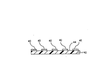
図1に示すように、RFIDアンテナなどの導電のパターン化された金属フィルムを製造する方法は、剥離被覆剤20層をベースポリマー物質22の可塑性層に塗布する工程と、剥離被覆剤20層上に導電性金属24層を溶着する工程とによって、中間体構造30を形成することを含んでなる。一実施形態に於いて、ベースポリマー物質22は、ポリエチレン若しくはポリエチレンテレフタレート(PET)等のポリオレフィン、ポリカーボネート等のポリエステル若しくは熱可塑性ポリエステル、ポリプロピレン、2軸配向されたポリプロピレン(BOPP)、ポリスルホンを1種単独又は2種以上混合したものであり得る。ベースポリマー物質22層は、ある適した厚さ、例えば約0.6ミル等の約0.1〜約10.0ミル、若しくは約10〜約100ゲージで形成され得る。
As shown in FIG. 1, a method of manufacturing a conductive patterned metal film, such as an RFID antenna, includes applying a release coating 20 layer to a plastic layer of a
図1を再び参照すると、剥離被覆剤20層は、その上に溶着した導電性金属24よりもベースポリマー物質22により一層密着するように形成されてなる。剥離被覆剤20は、熱若しくはエネルギーの硬化性物質を備え得る。剥離被覆剤20は、UV硬化性シリコン樹脂等のUV硬化性被覆剤を備え得る。一実施形態に於いて、剥離被覆剤20は、ニトロセルロース、アクリル、エポキシ、ポリエステル、ポリエーテル、ケトン、ポリアミド、シリコン、エポキシアクリレート、シリコンアクリレート、ポリエステルアクリレート、ポリエーテルアクリレート、アクリル酸のエステル類、単機能性アクリレート樹脂類、及び/又は多機能性アクリレート樹脂類であり得る。他の実施形態に於いて、剥離被覆剤20は、ポリエステルアクリレートをベースとするオリゴマーアクリレートポリマー類、及び/又はポリエーテルアクリレート樹脂類の組み合わせであり得る。剥離被覆剤20は、フレキソ印刷工程等の印刷プレスアプリケーションを用いることにより、ポリエチレンテレフタレート(PET)フィルム等のベースポリマー物質22に塗布される。剥離被覆剤20は、塗膜3000平方フィート当たり0.025〜5.0lbs、具体的には、塗膜3000平方フィート当たり1.0〜2.5lbsの厚さで塗布され得る。一実施形態に於いて、剥離被覆剤20は、液状で塗布される。それは、限定されるものではないが例えば、フレキソ印刷、グラビア印刷、ロール塗布、スクリーン印刷、石版印刷プレスでのインクトレインアプリケーション等を含む標準的な方法を用いて塗布される。
Referring again to FIG. 1, the
図1を再度参照すると、導電性金属24層は、剥離被覆剤20の硬化された層上に溶着される。いくつかの工程は、剥離被覆剤20層上に該金属を溶着するのに使用され得る。一実施形態に於いて、導電性金属24は、市販の真空めっき技術によって剥離被覆剤20の表面に溶着され得る。他の実施形態に於いて、導電性金属24は、市販の金属スパッタリング技術によって剥離被覆剤20の表面に溶着され得る。導電性金属24層は、銅、銀、及び/又はアルミニウムで形成され得る。導電性金属24層の厚さは、それぞれ特有の金属若しくは金属の組み合わせが必要な導電特性をもたらすのに異なる溶着の厚さを要求するため、用いられる金属若しくは金属の組み合わせに依存する。導電性金属24の厚さが導電パターンに対する最後のアプリケーションに依存するので、適切な厚さは様々あり得る。RFIDアンテナに対して推奨されているように、その厚さは、13.56MHzシステムで用いられるアンテナに対して約13〜約18ミクロンのオーダーであり、900MHzシステムで用いられるアンテナに対して約3ミクロンのオーダーであり、2.45GHzシステムで用いられるアンテナに対して約3ミクロン未満のオーダーであり得る。一実施形態に於いて、導電性金属24層は、約5から約30,000オングストローム又はそれ以上までの厚さで溶着され得る。他の実施形態に於いて、導電性金属24層は、約5〜約1,000オングストロームの厚さで溶着され得る。導電性金属24層は、毎分約5’〜約1,000’の速度で溶着され得る。しかしながら、これらの厚さは単なる例示であり、他の様々な厚さを有する導電パターンが採用されてもよいことは理解され得る。
Referring again to FIG. 1, the
図1を再び参照すると、一実施形態に於いて、導電性金属24層の光学密度は、約1〜100光学密度であり得る。他の実施形態に於いて、導電性金属24の表面抵抗率は、約0.01〜約1,000Ω/Sqであり得る。導電性金属24層が有する抵抗が低いほど、もたらされる導電パターンがより効率的になり得るということは理解される。この金属層の溶着は、50から30,000オングストローム若しくはそれ以上までであり得る。より具体的には、この金属は、200〜1,000オングストロームで溶着される。例えば、導電性金属24層は、250オングストロームの厚さ、3光学密度、1.18Ω/Sqの表面抵抗率を備え得るが、それは、可視光の0.1000透過率をもたらす。
Referring back to FIG. 1, in one embodiment, the optical density of the
図1に示すような中間体構造30から所望の基材上に導電性金属24を転写するために、図2に示すように、接着剤層40は、選択パターンにおけるターゲット基材42に塗布される。一実施形態に於いて、この選択パターンは、RFIDアンテナの形であり得る。他の実施形態に於いて、この選択パターンは、RFIDアンテナの逆パターンの形であり得る。接着剤層40は導電性ではないが、それは導電性経路のパターンにおけるターゲット基材42上に印刷される。一実施形態に於いて、接着剤層40は、エネルギー硬化性アクリレート樹脂類、アクリル酸のエステル類、単機能性アクリレート樹脂類、及び/又は多機能性アクリレート樹脂類を含み得る。他の実施形態に於いて、接着剤層40は、ポリエステルアクリレートをベースとするオリゴマーアクリレートポリマー類、及び/又はポリエーテルアクリレート樹脂類の組み合わせを含み得る。接着剤層40は、ターゲット基材42の表面44上に、厚さ約0.05〜約5ミルで溶着され得る。接着剤層40は、水ベース、溶媒ベース、若しくは固体層であり得る。
To transfer the
図2を再び参照すると、ターゲット基材42は、RFIDタグ若しくはラベルを形成するのに適したある物質を備え得る。一実施形態に於いて、ターゲット基材42は、ポリエステル、PET、ポリプロピレン、ポリオレフィン、ポリカーボネート、及び/又はポリスルホン等の透明なポリマー物質を備え得る。他の実施形態に於いて、ターゲット基材42は、紙、フィルム、板、ラベル、及び/又はタグストックを備え得る。ターゲット基材42は、後述するようにそれが印刷プレスのロールを通過され得るように、物質的に変形可能である。
Referring again to FIG. 2, the
図3に示すように、接着剤層40は、フレキソ印刷工程56によってターゲット基材42に塗布され得る。この実施形態に於いて、供給ロール48は、接着剤リザーバー46で回転して、アニロックスロール50に転写するために接着剤を取り上げる。アニロックスロール50は、プレートシリンダー52に接着剤を供給すべく複数の彫られたセルを備えてなる。ターゲット基材42は、プレートシリンダー52とインプレッションシリンダー54との間を通過される。プレートシリンダー52の表面は、アニロックスロール50から接着剤を取り上げ、それをターゲット基材42に転写する。インプレッションシリンダー54は、それがターゲット基材42の表面が接着剤を正確な導電性経路パターンで受けるのを認めるべくプレートシリンダー52と接触するように、ターゲット基材42を支える。他の実施形態に於いて、接着剤は、スクリーン印刷、グラビア印刷、オフセット印刷、活版印刷、デジタル、インクジェット、平版、ロータリースクリーン、フラットスクリーン、若しくはパッド印刷等の他の従来の手段によってターゲット基材に塗布され、そして、ロール・トゥー・ロールアプリケーション、若しくはシートフィードアプリケーションで塗布される。
As shown in FIG. 3, the
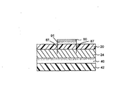
図4に示すように、いったん接着剤リザーバー46は、ターゲット基材42に塗布されると、ターゲット基材42は、図1に示すような中間体構造30に結合若しくは積層される。中間体構造30及びターゲット基材42は、ニップローラー58を通過し、ターゲット基材42の接着剤リザーバー46は、中間体構造30の導電性金属(符号24として図1に示されている)層に接触する。結果もたらされる結合構造60は、図5に示されているが、ここでは、ベースポリマー物質22、剥離被覆剤20層、導電性金属24層を含有する中間体構造30が、ターゲット基材42及び接着剤層40と結合されてなる。
As shown in FIG. 4, once the
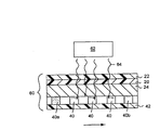
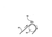
図6、7に示すように、その後、結合構造60は、結合構造の中にエネルギー波64を透過することによって接着剤層40を乾燥若しくは硬化するように、従来の硬化ユニット62を通過され得る。一実施形態に於いて、硬化ユニット62は、対流式オーブン、紫外線(UV)、硬化ランプ、電子ビーム(EB)硬化ユニット、若しくはエネルギー硬化性接着剤を硬化するために設計されたその他の従来のユニットであり得る。一実施形態に於いて、結合構造60は、結合構造60が硬化ユニット62を通されるように示された方向でローラー66上を通される。結合構造60が硬化ユニット62を通るように方向づけられるので、エネルギー波64は、ベースポリマー物質22、剥離被覆剤20、及び導電性金属24を通過し、ターゲット基材42に担持された接着剤層40の中を通る。結合構造60は、硬化ユニット62を通過するので、接着剤層40の未硬化部分40aが硬化された部分40bになる。また、ターゲット基材42が硬化ユニット62に近づく方向に向かわされるように、結合構造60が逆さの位置で硬化ユニット62を透過し得るとここでは予想される。
As shown in FIGS. 6 and 7, the
図8、9に示すように、結合構造60がいったん硬化されて、結合構造60は、ローラー66を通過し次ぎに剥離ローラー72を通過される。結合構造が剥離ローラー72を通過する時に、ベースポリマー物質22、剥離被覆剤20層、及び導電性金属24層の非対応部分68、集合的には廃棄部分76が、ターゲット基材42及び硬化された接着剤層40bから除去される。硬化された接着剤層40bに接する導電性金属24層の対応部分70のみが、ターゲット基材42と層状に関連し、集合的には導電パターン化されたフィルム74となる。導電パターン化されたフィルム74は、接着剤層40の事前に選択された形に対応する導電性金属の経路を含んでなる。一実施形態に於いて、導電パターン化されたフィルム74は、RFIDタグやラベル等のRFID装置のためのアンテナ等の電気部品である。他の実施形態に於いて、導電パターン化されたフィルム74は、コンピューターチップ若しくはコンピューターチップの部分である。さらに他の実施形態に於いて、導電パターン化されたフィルム74は、ケーブル回線若しくはプリント基板である。このようなケーブル及び回路基板は、良い解像度と、プラスチック若しくは可塑性基材に載置された導電性が可塑性を有するような配列であることとをしばしば要求する。
As shown in FIGS. 8 and 9, the
図10に示すように、中間体構造30の剥離被覆剤20のパフォーマンス特性の1つは、それが、剥離工程の間ベースポリマー物質22とともに無傷でいなければならず、また、導電性金属24の層の対応部分70に転写してはならないことである。
As shown in FIG. 10, one of the performance characteristics of the
図11に示すように、従来の剥離裏地120は、以前から箔装飾工程及び箔転写工程で用いられている。しかしながら、剥離工程では、従来の剥離裏地120が金属層124とベース層122との間で引き裂かれる。この剥離裏地120の引き裂きの影響は、非導電性剥離剤を生じ、例えば、それゆえに、金属層124とともに転写する剥離裏地120の部分が、表面134を非導電性にする。このプロセスは、箔転写技術を利用する他のアプリケーションには有効である一方で、導電性金属フィルム若しくは導電パターンを作製するには適していない。
As shown in FIG. 11, the conventional peeling lining 120 has been used in the foil decoration process and the foil transfer process for a long time. However, in the peeling process, the
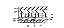
従って、図12に示すように、接着剤40は、ベースポリマー物質22に隣接する剥離被覆材20から導電性金属24層の対応部分70を完全に引っ張るほどの密着性を有する必要がないであろうことは理解される。一実施形態に於いて、下塗剤78の層は、接着剤40に対する未加工の金属表面の密着性を高めるべく伝導性金属24層の表面に塗布される。この下塗剤は、アクリル、ポリエステル、ポリアミド、エポキシ、又は金属表面の被覆剤の密着性を高めるのに適しているその他の樹脂を含み得る。一実施形態に於いて、この下塗剤は、約0.05〜約5ミルの厚さで導電性金属24の表面に溶着され得る。
Accordingly, as shown in FIG. 12, the adhesive 40 need not have sufficient adhesion to pull the corresponding
一実施形態に於いて、図13に示すように、本発明の導電パターン化されたフィルム74は、コンピューターチップ80に電気的に結合され得る。導電パターン化されたフィルム74は、導電性接着剤、若しくは導電性ストラップをはんだづけする工程等の従来の工程によって、コンピューターチップ80、若しくは他の電気部品に結びつけられる。一実施形態に於いて、導電パターン化されたフィルム74は、形成され、次ぎにコンピューターチップ80若しくは他の電気部品と結合される。しかしながら、他の実施形態に於いて、図14に示すように、エネルギー硬化性接着剤層40を塗布する前に、コンピューターチップ80若しくは電気部品を導電性金属24に転写することが望ましいであろう。
In one embodiment, the conductive patterned
図14に示すように、コンピューターチップ80若しくは電気部品は、挿入のストラップ方法を用いて、登録されたパターンにおける導電性金属層に直接付けられ得る。その後、感圧接着剤層40は、コンピューターチップ80若しくは電気部品上に塗布され、所望の導電パターンの形で、導電性金属24層、剥離被覆剤20層、及びベースポリマー物質22上に配置され得る。この複合材料構造82は、第二剥離裏地84上で巻かれ、その後、塗布での圧力を用いてターゲット基材86に分配され、その結果、完全なRFIDタグは、図13に示すようにプリントされた接着剤の形に分配される。
As shown in FIG. 14, a
導電パターン化されたフィルム74と、コンピューターチップ80若しくは電気部品との間における、導電性接着剤若しくは導電性ストラップの半田付け、溶着、若しくは接合は、剥離被覆剤20、84から導電パターン化されたフィルム74を除去する前、若しくはその除去後に起こる。導電パターン化されたフィルム74が、電気部品に接続することを要求されない分離された品物であることは理解され得る。例えば、導電パターン化されたフィルム74は、装飾的な若しくは視覚的に独特なアイテムとして用いられ得る。
The conductive adhesive or conductive strap soldering, welding, or bonding between the conductive patterned
他の実施形態に於いて、転写されたパターンを傷及び酸化から保護すべく、剥離被覆剤が導電性金属層の対応部分で完全に剥離するのを可能にすることは有効である。この実施形態に於いて、剥離被覆剤は、導電性金属層の対応部分で完全に剥離し、コンピューターチップは、直接的なチップ設置方法で剥離被覆剤上に設置される。 In other embodiments, it is useful to allow the release coating to completely peel at corresponding portions of the conductive metal layer to protect the transferred pattern from scratches and oxidation. In this embodiment, the release coating is completely released at the corresponding portion of the conductive metal layer, and the computer chip is placed on the release coating by a direct chip placement method.
図15、16に示すように、直接的なチップ設置方法は、通常、コンピューターチップ80の導電性リードに取り付けられ、導電性アンテナのリードの間にコンピューターチップ80から下方に向けて延びた導電性突起物若しくはピン87を備えてなるコンピューターチップ80を設置する工程を備えてなる。一実施形態に於いて、図16に示すように、導電性突起物若しくはピン87は、剥離被覆剤20と、接着剤層40及びターゲット基材42の近くに位置された導電性金属24とを貫通するように設置される。一実施形態に於いて、チップ80は、第二接着剤91とともに設置され得る、又は、コンピューターチップ上のターゲット基材の部分を溶解する熱によってターゲット基材に取付られ得る。コンピューターチップのリードは、剥離被覆剤を貫通するように設置され、導電性金属24層と接触する。
As shown in FIGS. 15 and 16, the direct chip placement method is usually performed by attaching a conductive lead of the
本発明は、好ましい実施形態を参照して記述されている。変更、組み合わせること、及び修正は、先行文献の詳細な記述を読むことで他者に浮かび得る。本発明が、変更、組み合わせること、修正等全てを含んでいると解釈されることは意図されている。 The invention has been described with reference to the preferred embodiments. Changes, combinations and modifications may emerge to others upon reading the detailed description of the prior art. It is intended that the present invention be construed to include all changes, combinations, modifications and the like.
Claims (24)
パターン化された接着剤層(40)をターゲット基材(42)の隣に供給する工程と、
前記導電性金属(24)層の対応部分(70)が前記パターン化された接着剤層(40)に接触するように、前記導電性金属(24)層と前記パターン化された接着剤層(40)とを接触させる工程と、
前記剥離被覆剤(20)から前記導電性金属(24)層の対応部分(70)を剥ぎ取るように前記パターン化された接着剤層(40)を利用する工程と備えてなる、導電パターン化されたフィルム(74)の製造方法。 Supplying a conductive metal (24) layer next to the release coating (20) layer;
Supplying a patterned adhesive layer (40) next to the target substrate (42);
The conductive metal (24) layer and the patterned adhesive layer (wherein the corresponding portion (70) of the conductive metal (24) layer is in contact with the patterned adhesive layer (40)). 40), and
Conductive patterning comprising the step of utilizing the patterned adhesive layer (40) to strip the corresponding portion (70) of the conductive metal (24) layer from the release coating (20). To produce a finished film (74).
前記導電性金属(24)層に電気部品(80)を直接付ける工程と、
RFIDアンテナの形にエネルギー硬化性接着剤層(40)をターゲット基材(42)に塗布する工程と、
前記導電性金属(24)層の対応部分(70)が前記エネルギー硬化性接着剤層(40)に接触するように、前記エネルギー硬化性接着剤層(40)及び前記導電性金属(24)を積層する工程とを備えてなり、
前記エネルギー硬化性接着剤層(40)が、前記導電性金属(24)層の対応部分(70)を前記剥離被覆剤(20)から剥離するRFIDアンテナの製造方法。 Supplying a conductive metal (24) layer next to the release coating (20) layer;
Directly attaching an electrical component (80) to the conductive metal (24) layer;
Applying an energy curable adhesive layer (40) to the target substrate (42) in the form of an RFID antenna;
The energy curable adhesive layer (40) and the conductive metal (24) are arranged such that the corresponding portion (70) of the conductive metal (24) layer contacts the energy curable adhesive layer (40). A process of laminating,
A method of manufacturing an RFID antenna, wherein the energy curable adhesive layer (40) peels the corresponding portion (70) of the conductive metal (24) layer from the release coating (20).
該ターゲット基材(42)に隣接するパターン化された接着剤層(40)と、
該パターン化された接着剤層(40)に隣接する導電性金属(24)層の対応部分(70)とを備えてなり、
該対応部分(70)が剥離被覆剤(20)層からの剥離によって構築され配置されてなるRFID装置。 A target substrate (42);
A patterned adhesive layer (40) adjacent to the target substrate (42);
A corresponding portion (70) of the conductive metal (24) layer adjacent to the patterned adhesive layer (40);
RFID device wherein the corresponding portion (70) is constructed and arranged by release from the release coating (20) layer.
Applications Claiming Priority (2)
| Application Number | Priority Date | Filing Date | Title |
|---|---|---|---|
| US74934905P | 2005-12-09 | 2005-12-09 | |
| PCT/US2006/046933 WO2007070391A1 (en) | 2005-12-09 | 2006-12-11 | Method and material for manufacturing electrically conductive patterns, including radio frequency identification (rfid) antennas |
Publications (2)
| Publication Number | Publication Date |
|---|---|
| JP2009520251A true JP2009520251A (en) | 2009-05-21 |
| JP2009520251A5 JP2009520251A5 (en) | 2010-03-11 |
Family
ID=37904891
Family Applications (1)
| Application Number | Title | Priority Date | Filing Date |
|---|---|---|---|
| JP2008544542A Pending JP2009520251A (en) | 2005-12-09 | 2006-12-11 | Methods and materials for making conductive patterns including radio frequency identification (RFID) antennas |
Country Status (8)
| Country | Link |
|---|---|
| US (1) | US20090250522A1 (en) |
| EP (1) | EP1964031A1 (en) |
| JP (1) | JP2009520251A (en) |
| KR (1) | KR20080095842A (en) |
| CN (1) | CN101341500B (en) |
| AU (1) | AU2006326694A1 (en) |
| CA (1) | CA2630834A1 (en) |
| WO (1) | WO2007070391A1 (en) |
Cited By (4)
| Publication number | Priority date | Publication date | Assignee | Title |
|---|---|---|---|---|
| JP2013015953A (en) * | 2011-07-01 | 2013-01-24 | Konica Minolta Business Technologies Inc | Method for manufacturing non-contact information recording medium |
| JP2015511182A (en) * | 2012-01-13 | 2015-04-16 | アルジョ ウイグギンス フイネ パペルス リミテッド | Method for manufacturing a sheet |
| JP2016179581A (en) * | 2015-03-24 | 2016-10-13 | トッパン・フォームズ株式会社 | Copying document |
| JP2016201068A (en) * | 2015-04-14 | 2016-12-01 | トッパン・フォームズ株式会社 | Manufacturing method of rfid medium |
Families Citing this family (36)
| Publication number | Priority date | Publication date | Assignee | Title |
|---|---|---|---|---|
| US6615189B1 (en) | 1998-06-22 | 2003-09-02 | Bank One, Delaware, National Association | Debit purchasing of stored value card for use by and/or delivery to others |
| US7809642B1 (en) | 1998-06-22 | 2010-10-05 | Jpmorgan Chase Bank, N.A. | Debit purchasing of stored value card for use by and/or delivery to others |
| US8793160B2 (en) | 1999-12-07 | 2014-07-29 | Steve Sorem | System and method for processing transactions |
| US7860789B2 (en) | 2001-07-24 | 2010-12-28 | Jpmorgan Chase Bank, N.A. | Multiple account advanced payment card and method of routing card transactions |
| US8020754B2 (en) | 2001-08-13 | 2011-09-20 | Jpmorgan Chase Bank, N.A. | System and method for funding a collective account by use of an electronic tag |
| US7899753B1 (en) | 2002-03-25 | 2011-03-01 | Jpmorgan Chase Bank, N.A | Systems and methods for time variable financial authentication |
| WO2003083619A2 (en) | 2002-03-29 | 2003-10-09 | Bank One, Delaware, N.A. | System and process for performing purchase transaction using tokens |
| US7809595B2 (en) | 2002-09-17 | 2010-10-05 | Jpmorgan Chase Bank, Na | System and method for managing risks associated with outside service providers |
| US20040122736A1 (en) | 2002-10-11 | 2004-06-24 | Bank One, Delaware, N.A. | System and method for granting promotional rewards to credit account holders |
| US8306907B2 (en) | 2003-05-30 | 2012-11-06 | Jpmorgan Chase Bank N.A. | System and method for offering risk-based interest rates in a credit instrument |
| US7401731B1 (en) | 2005-05-27 | 2008-07-22 | Jpmorgan Chase Bank, Na | Method and system for implementing a card product with multiple customized relationships |
| CA2642511C (en) * | 2007-11-02 | 2016-07-19 | Citicorp Credit Services, Inc. | Methods and systems for managing financial institution customer accounts |
| EP2335184A1 (en) * | 2008-10-15 | 2011-06-22 | Printechnologics GmbH | Planar data carrier |
| WO2010127509A1 (en) * | 2009-05-08 | 2010-11-11 | Confidex Ltd. | Rfid transponder |
| US8725589B1 (en) | 2009-07-30 | 2014-05-13 | Jpmorgan Chase Bank, N.A. | Methods for personalizing multi-layer transaction cards |
| FR2954361B1 (en) | 2009-12-23 | 2012-06-15 | Arjo Wiggins Fine Papers Ltd | ULTRA SMOOTH AND RECYCLABLE PRINTING SHEET AND METHOD OF MANUFACTURING THE SAME |
| US8480942B2 (en) * | 2010-01-27 | 2013-07-09 | The Board Of Trustees Of The University Of Illinois | Method of forming a patterned layer of a material on a substrate |
| USD623690S1 (en) | 2010-03-05 | 2010-09-14 | Jpmorgan Chase Bank, N.A. | Metal transaction device with gem-like surface |
| USD643064S1 (en) | 2010-07-29 | 2011-08-09 | Jpmorgan Chase Bank, N.A. | Metal transaction device with gem-like surface |
| CN103119663B (en) * | 2010-09-28 | 2015-06-24 | 三菱制纸株式会社 | Conductive material precursor and conductive material |
| CN103548037A (en) * | 2011-03-24 | 2014-01-29 | 泰格西斯赛斯公司 | RFID tag assembly and label process |
| CN103717387B (en) | 2011-08-03 | 2017-11-07 | 印刷包装国际公司 | System and method for forming the laminates with patterning microwave energy interactive material |
| FR2992663B1 (en) * | 2012-07-02 | 2015-04-03 | Arjo Wiggins Fine Papers Ltd | METHOD FOR MANUFACTURING A SHEET WITH A FACE HAVING AN AREA LARGER THAN THE REST OF THE FACE |
| FR2985744B1 (en) * | 2012-01-13 | 2014-11-28 | Arjo Wiggins Fine Papers Ltd | PROCESS FOR PRODUCING AN ELECTRO-CONDUCTIVE SHEET |
| US9038918B2 (en) * | 2012-12-13 | 2015-05-26 | Avery Dennison Corporation | Antenna for RFID device and method for making the same |
| USD854083S1 (en) | 2013-03-27 | 2019-07-16 | Jpmorgan Chase Bank, N.A. | Hybrid transaction device |
| US9977373B2 (en) | 2013-08-13 | 2018-05-22 | Hewlett-Packard Development Company, L.P. | Pattern foil printing |
| ES2702380T3 (en) * | 2013-09-26 | 2019-02-28 | Graphic Packaging Int Llc | Stratified, and systems and procedures for stratification |
| BR112017009698B1 (en) | 2014-12-22 | 2022-01-18 | Graphic Packaging International, Llc | METHOD FOR FORMING A LAMINATED, AND SYSTEM FOR FORMING A LAMINATED |
| CA3099249C (en) | 2018-05-03 | 2023-01-31 | Eric L. Bartholomew | Adhesive laminates and method for making adhesive laminates |
| CN108963422A (en) * | 2018-06-26 | 2018-12-07 | 中山国安火炬科技发展有限公司 | A kind of RFID antenna manufacturing process |
| US10813225B2 (en) | 2019-02-15 | 2020-10-20 | Xerox Corporation | Radio-frequency identification (RFID) label or conductive trace thermal transfer printing method |
| CN112312669B (en) * | 2019-07-26 | 2022-03-01 | 北京梦之墨科技有限公司 | Metal pattern, and preparation method and preparation device of metal pattern |
| CN114514534A (en) * | 2019-07-30 | 2022-05-17 | 艾利丹尼森零售信息服务有限公司 | Repositionable radio frequency identification device |
| CN110957556A (en) * | 2019-12-20 | 2020-04-03 | 江苏科睿坦电子科技有限公司 | Novel laser anti-counterfeiting ultrahigh frequency RFID (radio frequency identification) tag antenna and production process thereof |
| US11939478B2 (en) | 2020-03-10 | 2024-03-26 | Xerox Corporation | Metallic inks composition for digital offset lithographic printing |
Citations (6)
| Publication number | Priority date | Publication date | Assignee | Title |
|---|---|---|---|---|
| JPS60160692A (en) * | 1984-01-09 | 1985-08-22 | ストウフア− ケミカル カンパニ− | Transfer laminate of conductive metal layer and like |
| JPH0387089A (en) * | 1989-08-30 | 1991-04-11 | Nitto Denko Corp | Film for forming circuit pattern and manufacture of circuit board |
| JP2000048155A (en) * | 1998-07-31 | 2000-02-18 | Toppan Forms Co Ltd | Manufacture of non-contact ic module antenna |
| JP2001034732A (en) * | 1999-07-16 | 2001-02-09 | Toppan Forms Co Ltd | Formation of antenna for non-contact ic module |
| JP2003209421A (en) * | 2002-01-17 | 2003-07-25 | Dainippon Printing Co Ltd | Rfid tag having transparent antenna and production method therefor |
| JP2004342755A (en) * | 2003-05-14 | 2004-12-02 | Shinko Electric Ind Co Ltd | Method of manufacturing plane coil |
Family Cites Families (9)
| Publication number | Priority date | Publication date | Assignee | Title |
|---|---|---|---|---|
| US4012552A (en) * | 1975-03-10 | 1977-03-15 | Dennison Manufacturing Company | Decorative metal film heat transfer decalcomania |
| US5751256A (en) * | 1994-03-04 | 1998-05-12 | Flexcon Company Inc. | Resonant tag labels and method of making same |
| GB9709263D0 (en) * | 1997-05-07 | 1997-06-25 | Astor Universal Limited | Laminate structure |
| US6107920A (en) * | 1998-06-09 | 2000-08-22 | Motorola, Inc. | Radio frequency identification tag having an article integrated antenna |
| EP1035503B2 (en) * | 1999-01-23 | 2010-03-03 | X-ident technology GmbH | RFID-Transponder with printable surface |
| US20040200061A1 (en) * | 2003-04-11 | 2004-10-14 | Coleman James P. | Conductive pattern and method of making |
| EP1631857B1 (en) * | 2003-06-06 | 2007-03-07 | Sipix Imaging, Inc. | In mold manufacture of an object with embedded display panel |
| US7384496B2 (en) * | 2004-02-23 | 2008-06-10 | Checkpoint Systems, Inc. | Security tag system for fabricating a tag including an integrated surface processing system |
| US20070102103A1 (en) * | 2005-11-07 | 2007-05-10 | Klaser Technology Inc. | Manufacturing method for printing circuit |
-
2006
- 2006-12-11 WO PCT/US2006/046933 patent/WO2007070391A1/en active Application Filing
- 2006-12-11 AU AU2006326694A patent/AU2006326694A1/en not_active Abandoned
- 2006-12-11 CA CA002630834A patent/CA2630834A1/en not_active Abandoned
- 2006-12-11 KR KR1020087015850A patent/KR20080095842A/en not_active Application Discontinuation
- 2006-12-11 EP EP06839234A patent/EP1964031A1/en not_active Withdrawn
- 2006-12-11 JP JP2008544542A patent/JP2009520251A/en active Pending
- 2006-12-11 CN CN2006800462911A patent/CN101341500B/en not_active Expired - Fee Related
- 2006-12-11 US US12/095,056 patent/US20090250522A1/en not_active Abandoned
Patent Citations (6)
| Publication number | Priority date | Publication date | Assignee | Title |
|---|---|---|---|---|
| JPS60160692A (en) * | 1984-01-09 | 1985-08-22 | ストウフア− ケミカル カンパニ− | Transfer laminate of conductive metal layer and like |
| JPH0387089A (en) * | 1989-08-30 | 1991-04-11 | Nitto Denko Corp | Film for forming circuit pattern and manufacture of circuit board |
| JP2000048155A (en) * | 1998-07-31 | 2000-02-18 | Toppan Forms Co Ltd | Manufacture of non-contact ic module antenna |
| JP2001034732A (en) * | 1999-07-16 | 2001-02-09 | Toppan Forms Co Ltd | Formation of antenna for non-contact ic module |
| JP2003209421A (en) * | 2002-01-17 | 2003-07-25 | Dainippon Printing Co Ltd | Rfid tag having transparent antenna and production method therefor |
| JP2004342755A (en) * | 2003-05-14 | 2004-12-02 | Shinko Electric Ind Co Ltd | Method of manufacturing plane coil |
Cited By (5)
| Publication number | Priority date | Publication date | Assignee | Title |
|---|---|---|---|---|
| JP2013015953A (en) * | 2011-07-01 | 2013-01-24 | Konica Minolta Business Technologies Inc | Method for manufacturing non-contact information recording medium |
| JP2015511182A (en) * | 2012-01-13 | 2015-04-16 | アルジョ ウイグギンス フイネ パペルス リミテッド | Method for manufacturing a sheet |
| US9648751B2 (en) | 2012-01-13 | 2017-05-09 | Arjo Wiggins Fine Papers Limited | Method for producing a sheet |
| JP2016179581A (en) * | 2015-03-24 | 2016-10-13 | トッパン・フォームズ株式会社 | Copying document |
| JP2016201068A (en) * | 2015-04-14 | 2016-12-01 | トッパン・フォームズ株式会社 | Manufacturing method of rfid medium |
Also Published As
| Publication number | Publication date |
|---|---|
| EP1964031A1 (en) | 2008-09-03 |
| US20090250522A1 (en) | 2009-10-08 |
| CN101341500B (en) | 2011-03-02 |
| AU2006326694A1 (en) | 2007-06-21 |
| CA2630834A1 (en) | 2007-06-21 |
| KR20080095842A (en) | 2008-10-29 |
| WO2007070391A1 (en) | 2007-06-21 |
| CN101341500A (en) | 2009-01-07 |
Similar Documents
| Publication | Publication Date | Title |
|---|---|---|
| JP2009520251A (en) | Methods and materials for making conductive patterns including radio frequency identification (RFID) antennas | |
| US8191230B2 (en) | Method for making radio frequency (RF) antenna containing element | |
| US7477194B2 (en) | Conductive pattern and method of making | |
| US20050046573A1 (en) | Selective metal removal process for metallized retro-reflective and holographic films and radio frequency devices made therewith | |
| JP2015511352A (en) | Fragile high-frequency RFID electronic tag having a transfer prevention function and manufacturing method thereof | |
| JP2009520251A5 (en) | ||
| CN102958281A (en) | Method for preparing circuits on flexible base materials and application thereof | |
| CN1296728A (en) | Thin film transferable electric components | |
| US20030228748A1 (en) | Circuit elements having an ink receptive coating and a conductive trace and methods of manufacture | |
| JP2003298285A (en) | Reinforcing shield film and shield flexible printed wiring board | |
| US20020018880A1 (en) | Stamping foils for use in making printed circuits and radio frequency antennas | |
| US20050034995A1 (en) | Process for producing a structured metal layer on a substrate body, and substrate body having a structured metal layer | |
| JP2004054337A (en) | Ic chip mount body | |
| CN101296561B (en) | Flexible printing patchboard and sliding lid type mobile phone terminal using the same | |
| JPS63261892A (en) | Manufacture of printed circuit | |
| US20200406573A1 (en) | Method and arrangement for producing a label with integrated electrically conductive pattern | |
| CN1100999C (en) | Circuit-like metallic foil sheet for resonance frequency characteristic tag and the like and process for fabricating it | |
| CN202939631U (en) | Heat transfer RFID electronic label | |
| US9184491B2 (en) | Manipulation-proof RFID antenna having safety feature | |
| CN111201841A (en) | Method for depositing functional traces | |
| JP2019091777A (en) | Method for manufacturing circuit sheet | |
| JP3962119B2 (en) | Multilayer printed wiring board manufacturing sheet | |
| CN112020239B (en) | Electronic circuit and electronic circuit manufacturing method | |
| WO2005125290A1 (en) | A method for processing an electrically conductive pattern | |
| JP2015060504A (en) | Non-contact ic label |
Legal Events
| Date | Code | Title | Description |
|---|---|---|---|
| A521 | Request for written amendment filed |
Free format text: JAPANESE INTERMEDIATE CODE: A523 Effective date: 20091210 |
|
| A621 | Written request for application examination |
Free format text: JAPANESE INTERMEDIATE CODE: A621 Effective date: 20091210 |
|
| A521 | Request for written amendment filed |
Free format text: JAPANESE INTERMEDIATE CODE: A523 Effective date: 20100119 |
|
| A977 | Report on retrieval |
Free format text: JAPANESE INTERMEDIATE CODE: A971007 Effective date: 20120222 |
|
| A131 | Notification of reasons for refusal |
Free format text: JAPANESE INTERMEDIATE CODE: A131 Effective date: 20120224 |
|
| A02 | Decision of refusal |
Free format text: JAPANESE INTERMEDIATE CODE: A02 Effective date: 20120831 |