JP2009094149A - Multilayered inductor - Google Patents
Multilayered inductor Download PDFInfo
- Publication number
- JP2009094149A JP2009094149A JP2007261070A JP2007261070A JP2009094149A JP 2009094149 A JP2009094149 A JP 2009094149A JP 2007261070 A JP2007261070 A JP 2007261070A JP 2007261070 A JP2007261070 A JP 2007261070A JP 2009094149 A JP2009094149 A JP 2009094149A
- Authority
- JP
- Japan
- Prior art keywords
- coil
- magnetic
- gap
- inductor
- multilayer inductor
- Prior art date
- Legal status (The legal status is an assumption and is not a legal conclusion. Google has not performed a legal analysis and makes no representation as to the accuracy of the status listed.)
- Pending
Links
Images


Landscapes
- Coils Or Transformers For Communication (AREA)
Abstract
Description
本発明は、積層した磁性体によって磁気回路を構成する積層インダクタに関し、特に、磁気回路の一部に非磁性体による磁気ギャップ層を設けた積層インダクタに関する. The present invention relates to a multilayer inductor in which a magnetic circuit is constituted by laminated magnetic materials, and more particularly to a multilayer inductor in which a magnetic gap layer made of a nonmagnetic material is provided in a part of a magnetic circuit.
最近の携帯電話を代表とする携帯電子機器には、さまざまな機能モジュールが組み込まれている。しかしモジュールごとに必要とする電源電圧が異なるため、元となるバッテリー(たとえばリチウムイオン電池)の電源電圧から、モジュールが必要とする電圧へ変換する電圧変換回路、すなわちDC−DCコンバーターがモジュールごとに必要となる。 Various functional modules are incorporated in portable electronic devices such as recent cellular phones. However, since the power supply voltage required for each module differs, a voltage conversion circuit for converting the power supply voltage of the original battery (for example, a lithium ion battery) to the voltage required for the module, that is, a DC-DC converter is provided for each module. Necessary.
DC−DCコンバーターの中で電圧を変換する素子がインダクタである。従来フェライトのドラムコアに絶縁皮膜されたマグネットワイヤを巻線し、更にドラムコアを筒状のフェライトコアで囲んで構成される巻線タイプのインダクタが広く用いられていた。 An element that converts voltage in the DC-DC converter is an inductor. Conventionally, a winding type inductor in which a magnet wire coated with an insulating film is wound around a ferrite drum core and the drum core is surrounded by a cylindrical ferrite core has been widely used.
しかし、その構造上の問題から、小型化・低背化・低コスト化には限界があり、これに置き換わる物として、モノリシックで閉磁路構造の積層インダクタが注目されている。 However, due to structural problems, there are limits to miniaturization, low profile, and low cost, and monolithic, closed magnetic circuit multilayer inductors are attracting attention as an alternative.
積層インダクタは、磁性体(フェライト)と内部コイルパターン(Ag)とをシート積層法や印刷法などにより一体成型後、同時焼成して作成される。また、モノリシック(一体)構造となっているため、信頼性に優れ、小型化・低背化が容易であり、大量生産によるコストダウンと小型化によるコストダウンが容易であるという優れた特徴をもっている。 The multilayer inductor is formed by integrally firing a magnetic material (ferrite) and an internal coil pattern (Ag) by a sheet lamination method, a printing method, or the like, and simultaneously firing them. In addition, the monolithic (integral) structure has excellent characteristics such as high reliability, easy miniaturization and low profile, and easy cost reduction by mass production and cost reduction by miniaturization. .
しかし従来の積層インダクタは、磁性体であるフェライトをベースとした積層構造であるため、コイルパターンの層間に磁路が存在し、巻線インダクタのように磁束の流れが均一にならず、その結果高いインダクタンスや直流重畳特性を出しにくいという問題点があった。 However, since conventional multilayer inductors have a multilayer structure based on ferrite, which is a magnetic material, magnetic paths exist between the layers of the coil pattern, and the flow of magnetic flux is not uniform as in the case of wire wound inductors. There is a problem that high inductance and direct current superimposition characteristics are difficult to obtain.
これに対し、特許文献1の図2には各層のコイルパターン形成領域を非磁性体で埋めることにより、コイルパターン間に磁束を通さないようにした積層インダクタが開示されている。
しかし、シート積層法での成型は困難であり、印刷法であってもプロセスがに非常に複雑になり、低コスト化には適さない。
On the other hand, FIG. 2 of
However, it is difficult to form by the sheet lamination method, and even the printing method is very complicated, and is not suitable for cost reduction.
一方特許文献2の図2には、全コイル層もしくはそれに近いコイル層に磁気ギャップを分散して、各層のコイルが発生する磁束が、それぞれ各層の磁気ギャップを鎖交するようにして、直流重畳を向上し高周波磁束によるコイルパターン上の渦電流損失を低減したインダクタも開示されている。
On the other hand, in FIG. 2 of
図11は、特許文献2の積層インダクタ40の一例の断面図であり、磁性体2(フェライト)にコイルパターン5、6、7が形成された複数のコイル層を積層しており、外部引出しリード部15を除くコイル層に非磁性体による磁気ギャップ4が設けられている。
特許文献1に開示されている積層インダクタの構成では、コイルパターンを形成した磁性体層を積層して製造するシート積層法による製造が困難である。また印刷法であっても印刷プロセスが複雑になるという問題がある。
With the configuration of the multilayer inductor disclosed in
また、特許文献2の構成では、今後DC−DCコンバーターの高周波数化に伴う低インダクタンス化に対しコイルのターン数を低減していく場合、コイル層数が減り前記磁気ギャップの分散数が減って十分な分散効果が得られず前記渦電流損失が増大するという問題がある。図11の例では3ターンのインダクタであるがこの場合ギャップ分散数は最大3(引き出しリード部15含めれば4)となる。そのため、磁気ギャップの厚みを、コイルパターンの厚みに比べ十分薄くすることができなくなる。その結果、磁気ギャップの端面近傍で発生する磁束のフリンジング(広がり)がコイルパターンを鎖交し渦電流損失の原因となる。
Further, in the configuration of
本発明は斯かる事情に鑑みてなされたものであり、高周波数化に伴いコイルのターン数が減っても、十分な磁気ギャップの分散が可能であり、渦電流損失や直流抵抗による損失を低減でき、その結果Qが高くDC−DCコンバーターの高効率化に寄与する積層インダクタを提供することを目的とする。 The present invention has been made in view of such circumstances, and even if the number of turns of the coil is reduced as the frequency is increased, a sufficient magnetic gap can be dispersed, and eddy current loss and loss due to DC resistance are reduced. Therefore, an object of the present invention is to provide a multilayer inductor that has a high Q and contributes to high efficiency of a DC-DC converter.
本発明に係る積層インダクタは、磁性体層および第1のコイルパターンを交互に積層し、前記第1のコイルパターンを積層方向に直列接続してコイルを構成し、前記第1のコイルパターンに接する領域に第1の磁気ギャップパターンが形成され、積層方向に複数の磁気ギャップをもつ積層インダクタにおいて、一部または全ての前記第1のコイルパターンに対し並列接続された第2のコイルパターンを備え、該第2のコイルパターンに接する領域に第2の磁気ギャップパターンが形成されたことを特徴とする積層インダクタである。 In the multilayer inductor according to the present invention, magnetic layers and first coil patterns are alternately stacked, and the first coil patterns are connected in series in the stacking direction to form a coil, which is in contact with the first coil pattern. A laminated inductor having a plurality of magnetic gaps in the laminating direction, wherein a first magnetic gap pattern is formed in the region, and a second coil pattern connected in parallel to a part or all of the first coil patterns; The multilayer inductor is characterized in that a second magnetic gap pattern is formed in a region in contact with the second coil pattern.
したがって本発明の積層インダクタは、コイルのターン数が少ない場合であっても、十分な磁気ギャップの分散が可能であり、一ギャップあたりのギャップ長をコイルパターンの厚みより十分小さく設定することができる。その結果、ギャップ部における磁束のフリンジングは低減し、コイルパターンへ鎖交する磁束による渦電流損失を低減することができる。 Therefore, the multilayer inductor of the present invention can sufficiently disperse the magnetic gap even when the number of turns of the coil is small, and the gap length per gap can be set sufficiently smaller than the thickness of the coil pattern. . As a result, the fringing of the magnetic flux in the gap portion is reduced, and eddy current loss due to the magnetic flux interlinking with the coil pattern can be reduced.
本発明の積層インダクタは、磁気ギャップがコイルに囲まれた内側部分に形成されておりインダクタ端面に露出していないので、インダクタからの磁束の漏れが少なく、またこの漏れ磁束が外部電極と鎖交して生じる渦電流損失を低減することができる。 In the multilayer inductor of the present invention, the magnetic gap is formed in the inner part surrounded by the coil and is not exposed at the end face of the inductor, so there is little leakage of the magnetic flux from the inductor, and this leakage magnetic flux is linked to the external electrode. Thus, the eddy current loss that occurs can be reduced.
本発明の積層インダクタは、前記磁性体がNiZn系またはNiCuZnフェライトで、前記磁気ギャップがジルコニア(ZrO2)で形成されていることを特徴とする。 The multilayer inductor according to the present invention is characterized in that the magnetic body is NiZn-based or NiCuZn ferrite, and the magnetic gap is formed of zirconia (ZrO 2 ).
したがって本発明の積層インダクタは、前記磁性体がNiZn系またはNiCuZn系フェライトで、前記磁気ギャップがジルコニア(ZrO2)で形成されているので、磁性体と磁気ギャップを形成する異材質が反応することなく、設計値どおりの安定したインダクタ特性が得られる。 Therefore, in the multilayer inductor according to the present invention, the magnetic material is NiZn-based or NiCuZn-based ferrite, and the magnetic gap is formed of zirconia (ZrO 2 ), so that the magnetic material and a different material forming the magnetic gap react. And stable inductor characteristics as designed.
本発明の積層インダクタは、前記磁性体がNiZn系またはNiCuZn系フェライトで、前記磁気ギャップがZnフェライトで形成されていることを特徴とする。 The multilayer inductor of the present invention is characterized in that the magnetic material is NiZn-based or NiCuZn-based ferrite, and the magnetic gap is formed of Zn ferrite.
したがって本発明の積層インダクタは、前記磁性体であるNiZn系フェライトと前記磁気ギャップであるZnフェライトとの異材質間の同時焼成が容易で、デラミやクラック等が発生しにくい。 Therefore, in the multilayer inductor of the present invention, simultaneous firing between different materials of the NiZn-based ferrite that is the magnetic material and the Zn ferrite that is the magnetic gap is easy, and delamination and cracks are less likely to occur.
以下、本発明をその実施の形態を示す図面に基づいて詳述する。
(第1実施の形態)
図1は、第1実施の形態に係る積層インダクタ10の断面図、図2は第1の実施の形態に係る積層インダクタ10の分解斜視図である。
Hereinafter, the present invention will be described in detail with reference to the drawings illustrating embodiments thereof.
(First embodiment)
FIG. 1 is a cross-sectional view of the
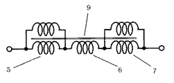
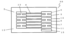
コイル層は例えばNiCuZnフェライトからなる磁性体2に、導電性材料例えばAgからなる略1ターンのコイルパターン5、6、7と、非磁性体材料例えばジルコニア(ZrO2)からなる磁気ギャップパターン4とを形成して構成される。第1のコイルパターン5、6、7が形成されたコイル層を積層しビアホール8を介して直列に接続する。また、その積層体の上下のコイル層5、7と略同構成の第2のコイルパターン9、11が形成されたコイル層を、それぞれ積層しビアホール12を介して並列に接続する。このように構成されたコイルは外部引出しリード部15と外部引き出し部1により外部へ引き出される。更にその積層体の上下にそれぞれ例えばNiCuZnフェライトからなる磁性体2のみの無地の磁性体層13を複数層ずつ重ねた態様で、3ターンの積層インダクタ10が構成されている。積層インダクタ10は、LTCC(Low Temperature Co−fired Ceramics)法による形成が好ましい。
The coil layer is made of, for example, a
この第1実施の形態の積層インダクタでは、上下のコイルパターン5、7は略同一形状のコイル9、11とスルーホール12を介して並列接続されており、上中下の3コイルパターンは、スルーホール8を介して直列接続され、全体として3.5ターンのコイルとして機能する。電気的な接続回路図を図3に示す。
In the multilayer inductor according to the first embodiment, the upper and
各コイル層の磁性体2は例えば、ソフトフェライトのペーストを用いて、ドクターブレード法、カレンダーロール法などによりグリーンシート(乾燥後15〜60μm)を形成する。その上にAgなどを含む合金の導電ペーストを所定のコイルパターン3に乾燥後20〜50μm厚で100〜400μm幅に印刷または塗布する。さらに磁気ギャップとなるジルコニアやZnフェライト等の非磁性体ペーストを所定の磁気ギャップパターン4に印刷または塗布する。
For example, the
磁気ギャップパターンの乾燥後厚みは3μm以上でかつコイルパターンよりも薄くなることが好ましい。コイルパターンを構成するAgの乾燥後厚みが厚く、グリーンシート2とコイルパターン3の段差が大きい場合には、層間のデラミネーションや密着不足あるいはボイドの原因となる可能性があるため、磁気ギャップパターン4を覆うと共にコイルパターンの上面とほぼ同じ高さとなるよう、コイルパターンを除く領域に磁性体ペーストを印刷または塗布するのが好ましい。また、前記並列接続のためのビアホール12は第2のコイルパターンの巻き始めと巻き終わり近傍近くだけでなく、第2のコイルパターンの任意の位置に追加配置しても良い。
The dried thickness of the magnetic gap pattern is preferably 3 μm or more and thinner than the coil pattern. When the thickness of the Ag constituting the coil pattern is thick after drying and the step between the
以上のプロセスにより作られた各コイル層を複数層積層しビアホール8を介して直列に、ビアホール12を介して並列に接続する。更にその積層体の上下にそれぞれ例えばNiZnフェライトからなる磁性体2のみの無地の磁性体層13を複数層積層する。
A plurality of coil layers formed by the above process are stacked and connected in series via the
このようにして得られたグリーン状の積層体は800〜950℃で磁性体であるフェライトと導電体であるAgおよび非磁性体であるジルコニアあるいはZnフェライトを同時に焼成し20%程度収縮して焼結体となる。 The green laminate thus obtained was fired at 800 to 950 ° C. by simultaneously firing ferrite as a magnetic material, Ag as a conductor and zirconia or Zn ferrite as a non-magnetic material, and shrinking by about 20%. Become a unity.
本実施例ではコイルのターン数は3ターンであるにもかかわらずギャップ分散は5となり、一ギャップあたりのギャップ長を3/5に低減でき、コイルパターンの厚みより十分小さく設定することができる。従ってギャップ部における磁束のフリンジングは低減し、コイルパターンへ鎖交する磁束による渦電流損失を低減することができる。また3ターンのうちの2ターンが並列接続されているのでインダクタの直流抵抗を2/3に低減することができる。 In this embodiment, although the number of turns of the coil is 3, the gap dispersion is 5, the gap length per gap can be reduced to 3/5, and can be set sufficiently smaller than the thickness of the coil pattern. Therefore, the fringing of the magnetic flux in the gap portion is reduced, and the eddy current loss due to the magnetic flux interlinking with the coil pattern can be reduced. Further, since two of the three turns are connected in parallel, the DC resistance of the inductor can be reduced to 2/3.
(第2実施の形態)
図4は第2の実施の形態に係る積層インダクタの断面図である。本実施例は第1の実施の形態と同じく3ターンのコイルとして機能しているが上中下のコイル層5、6、7のうち中のコイル層6が略同一形状のコイル層14とビアホール12を介して並列接続されている。
(Second Embodiment)
FIG. 4 is a cross-sectional view of the multilayer inductor according to the second embodiment. Although this example functions as a three-turn coil as in the first embodiment, the
本実施例ではコイルパターンは3ターンであるにもかかわらずギャプ分散数は4となり、一ギャップあたりのギャプ長を3/4に低減できコイルパターンの厚みより十分小さく設定することができる。従ってギャップ部における磁束のフリンジングは低減し、コイルパターンへ鎖交する磁束による渦電流損失を低減することができる。また3ターンのうちの1ターンが並列接続されているのでインダクタの直流抵抗を5/6に低減することができる。 In this embodiment, although the coil pattern has 3 turns, the gap dispersion number is 4, and the gap length per gap can be reduced to 3/4, which can be set sufficiently smaller than the thickness of the coil pattern. Therefore, the fringing of the magnetic flux in the gap portion is reduced, and the eddy current loss due to the magnetic flux interlinking with the coil pattern can be reduced. Further, since one of the three turns is connected in parallel, the DC resistance of the inductor can be reduced to 5/6.
(第3実施の形態)
図5は第3の実施の形態に係る積層インダクタの断面図である。本実施例は第1の実施の形態と同じく3ターンのコイルとして機能しているが全てのコイル層5、6、7が略同一形状のコイル層9、14、11とビアホール12を介して並列接続されている。
(Third embodiment)
FIG. 5 is a cross-sectional view of the multilayer inductor according to the third embodiment. This example functions as a three-turn coil as in the first embodiment, but all the coil layers 5, 6, 7 are arranged in parallel with the coil layers 9, 14, 11 having substantially the same shape and via
本実施例ではコイルパターンは3ターンであるにもかかわらずギャプ分散数は6となり、一ギャップあたりのギャプ長を1/2に低減でき、コイルパターンの厚みより十分小さく設定することができる。従ってギャップ部における磁束のフリンジングは低減し、コイルパターンへ鎖交する磁束による渦電流損失を低減することができる。また全てのコイルパターンが並列接続されているのでインダクタの直流抵抗を1/2に低減することができる。 In this embodiment, although the coil pattern has 3 turns, the gap distribution number is 6, the gap length per gap can be reduced to ½, and can be set sufficiently smaller than the thickness of the coil pattern. Therefore, the fringing of the magnetic flux in the gap portion is reduced, and the eddy current loss due to the magnetic flux interlinking with the coil pattern can be reduced. Further, since all the coil patterns are connected in parallel, the DC resistance of the inductor can be reduced to ½.
以上のように並列接続されるコイルの位置や数は任意であり、並列されるコイル数が多ければ磁気ギャップの分散数が増え一ギャップあたりのギャップ長を短くすることにより、渦電流損失を低減できかつ直流抵抗も減らすことが可能である。 As described above, the position and number of coils connected in parallel are arbitrary, and if the number of coils connected in parallel is large, the number of magnetic gap dispersion increases and the gap length per gap is shortened to reduce eddy current loss. And the direct current resistance can be reduced.
次に、第1、2及び3実施の形態に係る積層インダクタの製造工程について説明する。 Next, the manufacturing process of the multilayer inductor according to the first, second and third embodiments will be described.
NiCuZnフェライトは、例えばFe2O3、ZnO、NiOおよびCuOを主成分とするフェライト組成物が用いられる。この仮焼粉末100重量%に対して、バインダーを10重量%加え、可塑剤および溶剤と共にボールミルにて混練して、磁性体合用スラリーを得る。このスラリーを、ドクターブレード法によるシート成型機を用いて厚み20μmのフェライトシートを成型する。 As the NiCuZn ferrite, for example, a ferrite composition containing Fe 2 O 3 , ZnO, NiO and CuO as main components is used. 10% by weight of a binder is added to 100% by weight of the calcined powder, and kneaded with a plasticizer and a solvent by a ball mill to obtain a slurry for magnetic material combination. Using this slurry, a ferrite sheet having a thickness of 20 μm is molded using a sheet molding machine using a doctor blade method.
成型した所定のフェライトシートにスルーホールを形成し、磁気ギャップとなる非磁性体のペースト状に加工されたジルコニアを所定の形状に印刷し、その後コイルパターンとなるペースト状に加工されたAgを略1ターンのコイルパターンとなるように所定のパターンに印刷してコイル層を得る。なお、このジルコニアおよびAgの印刷順序は逆であっても良い。また、ジルコニアおよびAgの印刷による段差を無くし積層性を向上させるため、フェライトシートと同材質のペーストを印刷することもできる。 Through holes are formed in a predetermined molded ferrite sheet, zirconia processed into a non-magnetic paste to be a magnetic gap is printed in a predetermined shape, and then the Ag processed into a paste to be a coil pattern is substantially omitted. A coil layer is obtained by printing a predetermined pattern so as to form a one-turn coil pattern. Note that the printing order of zirconia and Ag may be reversed. Moreover, in order to eliminate the level | step difference by the printing of a zirconia and Ag and to improve a laminating property, the paste of the same material as a ferrite sheet can also be printed.
このようにして形成されたコイル層を、前記ビアホール8を介して電気的に直列に、また前記ビアホール12を介して並列に、前記第1のコイルパターンと前記第2のコイルパターンとを所定のターン数とギャップ分散数が得られるよう、複数の無地のフェライトシート13の上に積層し、さらに積層された該コイル層の上に複数層の無地のフェライトシート13を積層する。得られた積層体を、一定圧力で圧着させた後に所望の形状に加工し、900℃で4時間大気中で焼成させ直方体(例えば2.5x2.0x1.0mm)の焼結体を得る。更にこの焼結体の向かい合う端面(例えば2.0x1.0mmの面)に外部電極用の導電ペースト(例えばAg)を塗布した後、更に630℃で15分の焼き付け処理をして、積層インダクタを得る。
The coil layer thus formed is electrically connected in series via the via
以上のようにして、本発明では、ターン数が少ないインダクタであっても、一部もしくは全てのコイルパターンに対し並列に接続されたコイルパターンを印刷された層が設けられており、並列接続されたコイルパターンの数だけ多くの磁気ギャップの分散が可能となる。そのため、ターン数が少なくても、十分な磁気ギャップ分散が得られ渦電流損失が抑えることができる。更に、並列接続されたコイルによりインダクタの直流抵抗も低減することができる。 As described above, in the present invention, even for an inductor having a small number of turns, a layer printed with a coil pattern connected in parallel to a part or all of the coil patterns is provided and connected in parallel. As many magnetic gaps as the number of coil patterns can be dispersed. Therefore, even if the number of turns is small, sufficient magnetic gap dispersion can be obtained and eddy current loss can be suppressed. Further, the DC resistance of the inductor can be reduced by the coils connected in parallel.
従来の図11の積層インダクタと図1の本発明の積層インダクタについて、コイルパターンを鎖交する磁束密度を計算した。従来の積層インダクタの構成は、巻数は3ターンで最上コイル層以外の3コイル層に合計30μmのギャップを分散している。一方、本発明の積層インダクタの構成は、巻数は同じ3ターンであるがその内の2ターンに並列接続されたコイル層が追加されており、追加された2コイル層含め5コイル層に合計30μmのギャップを分散している。シミュレーションは日本総研ソリューションズの電磁界解析ソフトJ−MAG Ver8.4を用い、周波数2MHz、励磁電流0.1Appの条件で実施した。 For the conventional multilayer inductor of FIG. 11 and the multilayer inductor of the present invention of FIG. 1, the magnetic flux density interlinking the coil patterns was calculated. In the conventional multilayer inductor, the number of turns is 3 turns, and a total gap of 30 μm is dispersed in the three coil layers other than the uppermost coil layer. On the other hand, the configuration of the multilayer inductor of the present invention has the same number of turns of 3 turns, but a coil layer connected in parallel to 2 turns is added, and a total of 30 μm is added to 5 coil layers including the added 2 coil layers. The gap is dispersed. The simulation was performed using the electromagnetic field analysis software J-MAG Ver8.4 of Japan Research Institute Solutions under the conditions of a frequency of 2 MHz and an excitation current of 0.1 App.
コイルパターンを鎖交する磁束密度は、従来の積層インダクタの場合最大5。0mTであるが、本発明の積層インダクタの場合3.5mT程度となり30%程度低減していることがわかった。さらに渦電流損失を計算すると、従来の構造であれば2.98mWであるのに対し、本発明の構造は1.83mWとなり、40%程度渦電流損失が低減できることがわかった。 The magnetic flux density interlinking the coil pattern is 5.0 mT at the maximum in the case of the conventional multilayer inductor, but it is found that it is about 3.5 mT in the case of the multilayer inductor of the present invention, which is reduced by about 30%. Further, when the eddy current loss is calculated, it is 2.98 mW in the conventional structure, whereas the structure of the present invention is 1.83 mW, and it is found that the eddy current loss can be reduced by about 40%.
さらに従来の積層インダクタと本発明の積層インダクタとについて実際に素子を試作してその素子特性(Qの周波数特性、直流抵抗)および3MHzで動作するDC−DCコンバーターに適用した際の効率特性を測定した。 Furthermore, actual device prototypes of the conventional multilayer inductor and the multilayer inductor of the present invention were manufactured, and the device characteristics (Q frequency characteristics, DC resistance) and efficiency characteristics when applied to a DC-DC converter operating at 3 MHz were measured. did.
インダクタは、30μm厚のNiCuZn系の低温焼成フェライトを磁性材料としたシートに、Agペーストでコイルパターンを乾燥後40μm厚で360μm幅に印刷し、またジルコニアペーストでコイルパターンに囲まれた内側に乾燥後6μm厚で印刷した。このようにして作られたコイル層を複数所定のターン数およびギャップ分散数となるよう積層し、その後焼成しさらに外部電極を形成して積層インダクタを作成した。得られたインダクタの外形は、2.5x2.0x1.0mm、コイルの巻数は共に4.5ターンで巻き始めと終わりのコイル層以外の3コイル層に磁気ギャップを分散している。更に本発明の素子においてはその3コイル層のうち1コイル層に並列接続されたコイル層が追加挿入されており、計4コイル層にギャップが分散されている。図6に、その断面図を示している。図より従来の積層インダクタはギャップ分散数が3、本発明の積層インダクタはギャップ分散数が4となる。 The inductor is a 30 μm-thick NiCuZn-based low-temperature-fired ferrite magnetic sheet, and the coil pattern is dried with Ag paste, then printed to a width of 360 μm with a thickness of 40 μm, and dried inside the coil pattern with zirconia paste. After printing with a thickness of 6 μm. A plurality of coil layers thus produced were laminated so as to have a predetermined number of turns and gap dispersion numbers, and then fired to form external electrodes, thereby producing a laminated inductor. The outer shape of the obtained inductor is 2.5 × 2.0 × 1.0 mm, the number of turns of the coil is 4.5 turns, and the magnetic gap is distributed in three coil layers other than the coil layer at the start and end of winding. Further, in the element of the present invention, a coil layer connected in parallel to one coil layer among the three coil layers is additionally inserted, and the gap is dispersed in a total of four coil layers. FIG. 6 shows a cross-sectional view thereof. From the figure, the conventional multilayer inductor has a gap dispersion number of 3, and the multilayer inductor of the present invention has a gap dispersion number of 4.
以下その測定結果について詳述する。まずQの周波数特性はアジレントテクノロジーの4285Aを用いて70kHzから30MHzの周波数範囲内で励磁振幅1Vで測定した。結果を図7に示す.本発明の積層インダクタは従来の積層インダクタに比べ、最大値で比較すると29%向上した。
次に、直流抵抗の測定はアジレントテクノロジーの3458Aを用いて4端子法にて測定した。従来の積層インダクタは75mΩであったが、本発明の積層インダクタは67mΩ、となり12%低減した。
The measurement results will be described in detail below. First, the frequency characteristics of Q were measured with an excitation amplitude of 1 V within a frequency range of 70 kHz to 30 MHz using Agilent Technologies 4285A. The results are shown in Fig. 7. The multilayer inductor of the present invention improved by 29% compared to the conventional multilayer inductor at the maximum value.
Next, the DC resistance was measured by a four-terminal method using Agilent Technology 3458A. The conventional multilayer inductor was 75 mΩ, but the multilayer inductor of the present invention was 67 mΩ, a 12% reduction.
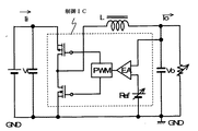
次に3MHzで動作するDC−DCコンバーターの回路構成を図8に示す。出力電圧Voは基準電圧Refと誤差増幅器EAにより比較増幅され、パルス幅変調回路PWMによりパルス幅に変調され2個のMOSFETのゲートに与えられ3MHzの周波数で2個のMOSFETを相補的にオンオフさせる。2個のMOSFETのスイッチング動作により、入力電圧ViはインダクタLを介して降圧され必要な出力電圧Voを得る。本回路のインダクタ素子Lを従来の積層インダクタを用いた場合と、本発明の積層インダクタを用いた場合とでDC−DCコンバーターの変換効率ηを出力電流を変化させて測定した。ここで入力電流をIi、出力電流をIoとすれば、η=VoxIo/(VixIi)x100(%)で求めることができる。Vi=3.6V、Vo=1.8Vの降圧形DC−DCコンバーターとして動作させた場合の結果を図9に示す。共に効率が出力電流が100mA近傍で急激に変化しているが、これはこの出力電流を境界に、制御ICの出力電圧の制御モードが変化しているためである。 Next, FIG. 8 shows a circuit configuration of a DC-DC converter operating at 3 MHz. The output voltage Vo is compared and amplified by the reference voltage Ref and the error amplifier EA, modulated to a pulse width by the pulse width modulation circuit PWM, applied to the gates of the two MOSFETs, and the two MOSFETs are complementarily turned on and off at a frequency of 3 MHz. . By the switching operation of the two MOSFETs, the input voltage Vi is stepped down through the inductor L to obtain a necessary output voltage Vo. The conversion efficiency η of the DC-DC converter was measured by changing the output current when the conventional multilayer inductor was used as the inductor element L of this circuit and when the multilayer inductor of the present invention was used. If the input current is Ii and the output current is Io, η = VoxIo / (VixIi) × 100 (%). FIG. 9 shows the results when operating as a step-down DC-DC converter with Vi = 3.6V and Vo = 1.8V. In both cases, the efficiency changes abruptly when the output current is in the vicinity of 100 mA. This is because the control mode of the output voltage of the control IC changes with this output current as a boundary.
本発明の積層インダクタは従来の積層インダクタに比べ、最大効率で0.8%、最大出力電流時で0.17%効率を向上できることがわかった。ここで最大効率時の効率向上は前述したQ特性の向上が、また最大出力電流時の効率向上は、前述した直流抵抗の低減が主に寄与している。 It was found that the multilayer inductor of the present invention can improve the efficiency by 0.8% at the maximum efficiency and 0.17% at the maximum output current as compared with the conventional multilayer inductor. Here, the improvement in efficiency at the maximum efficiency mainly contributes to the improvement of the Q characteristic described above, and the improvement in efficiency at the maximum output current mainly contributes to the reduction of the DC resistance described above.
以上のようにQの周波数特性、直流抵抗およびDC−DCコンバーターの効率において本発明は効果があることを確認したが、図10に示すように直流重畳特性が本発明により劣化することは無かった。 As described above, it was confirmed that the present invention is effective in the frequency characteristics of Q, the direct current resistance, and the efficiency of the DC-DC converter. However, the direct current superposition characteristics were not deteriorated by the present invention as shown in FIG. .
また磁気ギャップとしてジルコニアの代わりに、Fe2O3、ZnO、およびCuOを主成分とするZnフェライトを用いても同様な結果が得られた。 Similar results were obtained when Zn ferrite containing Fe 2 O 3 , ZnO, and CuO as main components was used as the magnetic gap instead of zirconia.
本発明によれば、磁気ギャップを分散して有する積層インダクタにおいて、そのターン数が少ない場合であっても、十分なギャップ分散数が得られるのでギャップ近傍のコイルパターンでの渦電流損失を低減できる。またコイル層の一部または全てが並列に接続されているので、インダクタの直流抵抗も低減できる。 According to the present invention, in a multilayer inductor having dispersed magnetic gaps, even if the number of turns is small, a sufficient number of gap dispersions can be obtained, so that eddy current loss in a coil pattern near the gap can be reduced. . In addition, since some or all of the coil layers are connected in parallel, the DC resistance of the inductor can also be reduced.
1 外部引き出し部
2 磁性体
4 磁気ギャップ
5 上コイル層
6 中コイル層
7 下コイル層
8 上中下のコイルパターンを直列に電気的に接続するビアホール
9 上コイル層と並列接続されるコイル層
10 第1の実施形態に係る積層インダクタの断面図
11 下コイル層と並列接続されるコイル層
12 上中下のコイルパターンと並列に電気的に接続するビアホール
13 無地の磁性体層
14 中コイルと並列接続されるコイル層
15 外部引出しリード部
20 第2の実施形態に係る積層インダクタの断面図
30 第3の実施形態に係る積層インダクタ断面図
40 従来の積層インダクタの断面図
DESCRIPTION OF
Claims (4)
一部または全ての前記第1のコイルパターンに対し並列接続された第2のコイルパターンを備え、該第2のコイルパターンに接する領域に第2の磁気ギャップパターンが形成されたことを特徴とする積層インダクタ。 A magnetic layer and a first coil pattern are alternately stacked, the first coil pattern is connected in series in the stacking direction to form a coil, and a first magnetic gap pattern is formed in a region in contact with the first coil pattern. In a multilayer inductor having a plurality of magnetic gaps in the stacking direction,
A second coil pattern connected in parallel to some or all of the first coil patterns is provided, and a second magnetic gap pattern is formed in a region in contact with the second coil pattern. Multilayer inductor.
Priority Applications (1)
| Application Number | Priority Date | Filing Date | Title |
|---|---|---|---|
| JP2007261070A JP2009094149A (en) | 2007-10-04 | 2007-10-04 | Multilayered inductor |
Applications Claiming Priority (1)
| Application Number | Priority Date | Filing Date | Title |
|---|---|---|---|
| JP2007261070A JP2009094149A (en) | 2007-10-04 | 2007-10-04 | Multilayered inductor |
Publications (1)
| Publication Number | Publication Date |
|---|---|
| JP2009094149A true JP2009094149A (en) | 2009-04-30 |
Family
ID=40665876
Family Applications (1)
| Application Number | Title | Priority Date | Filing Date |
|---|---|---|---|
| JP2007261070A Pending JP2009094149A (en) | 2007-10-04 | 2007-10-04 | Multilayered inductor |
Country Status (1)
| Country | Link |
|---|---|
| JP (1) | JP2009094149A (en) |
Cited By (12)
| Publication number | Priority date | Publication date | Assignee | Title |
|---|---|---|---|---|
| WO2011145517A1 (en) * | 2010-05-19 | 2011-11-24 | 株式会社村田製作所 | Electronic component |
| JP2013012741A (en) * | 2011-06-28 | 2013-01-17 | Samsung Electro-Mechanics Co Ltd | Gap layer composition of multilayered power inductor and multilayered power inductor including gap layer |
| JP2014116589A (en) * | 2012-12-11 | 2014-06-26 | Samsung Electro-Mechanics Co Ltd | Electronic component and method of manufacturing the same |
| US20140186526A1 (en) * | 2011-07-07 | 2014-07-03 | Inpaq Technology Co., Ltd. | Common mode filter and method of manufacturing the same |
| JP2015018852A (en) * | 2013-07-09 | 2015-01-29 | 東光株式会社 | Laminated electronic component |
| WO2015068613A1 (en) * | 2013-11-05 | 2015-05-14 | 株式会社村田製作所 | Laminated coil, impedance conversion circuit, and communication-terminal device |
| CN105408972A (en) * | 2013-08-13 | 2016-03-16 | 株式会社村田制作所 | Electronic component |
| JP2017199766A (en) * | 2016-04-26 | 2017-11-02 | 株式会社村田製作所 | Lamination coil array and module |
| JP2019192897A (en) * | 2018-04-26 | 2019-10-31 | サムソン エレクトロ−メカニックス カンパニーリミテッド. | Inductor |
| WO2021131478A1 (en) * | 2019-12-25 | 2021-07-01 | 株式会社村田製作所 | Multi-terminal chip inductor |
| CN113257510A (en) * | 2020-02-07 | 2021-08-13 | Tdk株式会社 | Coil component |
| JP2021144977A (en) * | 2020-03-10 | 2021-09-24 | 株式会社村田製作所 | Laminated coil component |
Citations (3)
| Publication number | Priority date | Publication date | Assignee | Title |
|---|---|---|---|---|
| JPH038311A (en) * | 1989-06-06 | 1991-01-16 | Nec Corp | Laminated transformer |
| JPH0557817U (en) * | 1991-12-28 | 1993-07-30 | 太陽誘電株式会社 | Multilayer chip inductor |
| WO2007088914A1 (en) * | 2006-01-31 | 2007-08-09 | Hitachi Metals, Ltd. | Laminated component and module using same |
-
2007
- 2007-10-04 JP JP2007261070A patent/JP2009094149A/en active Pending
Patent Citations (3)
| Publication number | Priority date | Publication date | Assignee | Title |
|---|---|---|---|---|
| JPH038311A (en) * | 1989-06-06 | 1991-01-16 | Nec Corp | Laminated transformer |
| JPH0557817U (en) * | 1991-12-28 | 1993-07-30 | 太陽誘電株式会社 | Multilayer chip inductor |
| WO2007088914A1 (en) * | 2006-01-31 | 2007-08-09 | Hitachi Metals, Ltd. | Laminated component and module using same |
Cited By (20)
| Publication number | Priority date | Publication date | Assignee | Title |
|---|---|---|---|---|
| WO2011145517A1 (en) * | 2010-05-19 | 2011-11-24 | 株式会社村田製作所 | Electronic component |
| US9460837B2 (en) | 2011-06-28 | 2016-10-04 | Samsung Electro-Mechanics Co., Ltd. | Gap composition of multi layered power inductor and multi layered power inductor including gap layer using the same |
| JP2013012741A (en) * | 2011-06-28 | 2013-01-17 | Samsung Electro-Mechanics Co Ltd | Gap layer composition of multilayered power inductor and multilayered power inductor including gap layer |
| US20140186526A1 (en) * | 2011-07-07 | 2014-07-03 | Inpaq Technology Co., Ltd. | Common mode filter and method of manufacturing the same |
| US9251953B2 (en) * | 2011-07-07 | 2016-02-02 | Inpaq Technology Co., Ltd. | Method of manufacturing a common mode filter |
| JP2014116589A (en) * | 2012-12-11 | 2014-06-26 | Samsung Electro-Mechanics Co Ltd | Electronic component and method of manufacturing the same |
| JP2015018852A (en) * | 2013-07-09 | 2015-01-29 | 東光株式会社 | Laminated electronic component |
| CN105408972A (en) * | 2013-08-13 | 2016-03-16 | 株式会社村田制作所 | Electronic component |
| US9698831B2 (en) | 2013-11-05 | 2017-07-04 | Murata Manufacturing Co., Ltd. | Transformer and communication terminal device |
| GB2537265A (en) * | 2013-11-05 | 2016-10-12 | Murata Manufacturing Co | Laminated coil, impedance conversion circuit, and communication-terminal device |
| WO2015068613A1 (en) * | 2013-11-05 | 2015-05-14 | 株式会社村田製作所 | Laminated coil, impedance conversion circuit, and communication-terminal device |
| GB2537265B (en) * | 2013-11-05 | 2018-07-18 | Murata Manufacturing Co | Impedance converting circuit, and communication terminal device |
| JP2017199766A (en) * | 2016-04-26 | 2017-11-02 | 株式会社村田製作所 | Lamination coil array and module |
| JP2019192897A (en) * | 2018-04-26 | 2019-10-31 | サムソン エレクトロ−メカニックス カンパニーリミテッド. | Inductor |
| US11270836B2 (en) | 2018-04-26 | 2022-03-08 | Samsung Electro-Mechanics Co., Ltd. | Inductor |
| WO2021131478A1 (en) * | 2019-12-25 | 2021-07-01 | 株式会社村田製作所 | Multi-terminal chip inductor |
| JP6908214B1 (en) * | 2019-12-25 | 2021-07-21 | 株式会社村田製作所 | Multi-terminal chip inductor |
| CN113257510A (en) * | 2020-02-07 | 2021-08-13 | Tdk株式会社 | Coil component |
| JP2021144977A (en) * | 2020-03-10 | 2021-09-24 | 株式会社村田製作所 | Laminated coil component |
| JP7151738B2 (en) | 2020-03-10 | 2022-10-12 | 株式会社村田製作所 | Laminated coil parts |
Similar Documents
| Publication | Publication Date | Title |
|---|---|---|
| JP2009094149A (en) | Multilayered inductor | |
| KR101372963B1 (en) | Laminated component and module using same | |
| JP5347973B2 (en) | Multilayer inductor and power converter using the same | |
| JP3621300B2 (en) | Multilayer inductor for power circuit | |
| JP4973996B2 (en) | Laminated electronic components | |
| JP5642036B2 (en) | Chip coil components | |
| EP1739695A1 (en) | Multilayer coil | |
| KR20100127878A (en) | Multilayer inductor and method for manufacturing the same | |
| JP5761610B2 (en) | Ceramic electronic component and method for manufacturing ceramic electronic component | |
| JP5181694B2 (en) | Electronic components | |
| KR101214731B1 (en) | Multilayer inductor and method of manifacturing the same | |
| JP5429649B2 (en) | Inductor built-in component and DC-DC converter using the same | |
| JPH1197256A (en) | Laminated chip inductor | |
| KR102030086B1 (en) | Stacked inductor | |
| JP2011091269A (en) | Laminated inductor | |
| JP2005259774A (en) | Open magnetic circuit type laminated coil component | |
| JP4400430B2 (en) | Multilayer inductor | |
| KR20130030573A (en) | Multilayer inductor and method of manifacturing the same | |
| JP6365805B2 (en) | DCDC converter module and DCDC converter circuit | |
| JP4893403B2 (en) | Inductor device and inductance adjusting method for the inductor device | |
| KR20150042169A (en) | Multilayer type inductor and method of manufacturing the same | |
| WO2009147899A1 (en) | Electronic part and method for manufacturing the same | |
| KR20130031083A (en) | Multilayer inductor | |
| KR101214701B1 (en) | Multilayer Power Inductor and Method of Manifacturing the same | |
| JP2015198159A (en) | multilayer inductor |
Legal Events
| Date | Code | Title | Description |
|---|---|---|---|
| A621 | Written request for application examination |
Free format text: JAPANESE INTERMEDIATE CODE: A621 Effective date: 20100611 |
|
| A521 | Written amendment |
Free format text: JAPANESE INTERMEDIATE CODE: A523 Effective date: 20110801 |
|
| A977 | Report on retrieval |
Effective date: 20120213 Free format text: JAPANESE INTERMEDIATE CODE: A971007 |
|
| A131 | Notification of reasons for refusal |
Effective date: 20120217 Free format text: JAPANESE INTERMEDIATE CODE: A131 |
|
| A521 | Written amendment |
Effective date: 20120405 Free format text: JAPANESE INTERMEDIATE CODE: A523 |
|
| A02 | Decision of refusal |
Effective date: 20121130 Free format text: JAPANESE INTERMEDIATE CODE: A02 |