JP2009075459A - Method for manufacturing biaxial birefringent material, biaxial birefringent material and liquid crystal projector - Google Patents
Method for manufacturing biaxial birefringent material, biaxial birefringent material and liquid crystal projector Download PDFInfo
- Publication number
- JP2009075459A JP2009075459A JP2007245921A JP2007245921A JP2009075459A JP 2009075459 A JP2009075459 A JP 2009075459A JP 2007245921 A JP2007245921 A JP 2007245921A JP 2007245921 A JP2007245921 A JP 2007245921A JP 2009075459 A JP2009075459 A JP 2009075459A
- Authority
- JP
- Japan
- Prior art keywords
- liquid crystal
- substrate
- vapor deposition
- phase difference
- refractive index
- Prior art date
- Legal status (The legal status is an assumption and is not a legal conclusion. Google has not performed a legal analysis and makes no representation as to the accuracy of the status listed.)
- Abandoned
Links
Images


Classifications
-
- G—PHYSICS
- G03—PHOTOGRAPHY; CINEMATOGRAPHY; ANALOGOUS TECHNIQUES USING WAVES OTHER THAN OPTICAL WAVES; ELECTROGRAPHY; HOLOGRAPHY
- G03B—APPARATUS OR ARRANGEMENTS FOR TAKING PHOTOGRAPHS OR FOR PROJECTING OR VIEWING THEM; APPARATUS OR ARRANGEMENTS EMPLOYING ANALOGOUS TECHNIQUES USING WAVES OTHER THAN OPTICAL WAVES; ACCESSORIES THEREFOR
- G03B21/00—Projectors or projection-type viewers; Accessories therefor
- G03B21/14—Details
-
- C—CHEMISTRY; METALLURGY
- C23—COATING METALLIC MATERIAL; COATING MATERIAL WITH METALLIC MATERIAL; CHEMICAL SURFACE TREATMENT; DIFFUSION TREATMENT OF METALLIC MATERIAL; COATING BY VACUUM EVAPORATION, BY SPUTTERING, BY ION IMPLANTATION OR BY CHEMICAL VAPOUR DEPOSITION, IN GENERAL; INHIBITING CORROSION OF METALLIC MATERIAL OR INCRUSTATION IN GENERAL
- C23C—COATING METALLIC MATERIAL; COATING MATERIAL WITH METALLIC MATERIAL; SURFACE TREATMENT OF METALLIC MATERIAL BY DIFFUSION INTO THE SURFACE, BY CHEMICAL CONVERSION OR SUBSTITUTION; COATING BY VACUUM EVAPORATION, BY SPUTTERING, BY ION IMPLANTATION OR BY CHEMICAL VAPOUR DEPOSITION, IN GENERAL
- C23C14/00—Coating by vacuum evaporation, by sputtering or by ion implantation of the coating forming material
- C23C14/06—Coating by vacuum evaporation, by sputtering or by ion implantation of the coating forming material characterised by the coating material
- C23C14/08—Oxides
- C23C14/083—Oxides of refractory metals or yttrium
-
- C—CHEMISTRY; METALLURGY
- C23—COATING METALLIC MATERIAL; COATING MATERIAL WITH METALLIC MATERIAL; CHEMICAL SURFACE TREATMENT; DIFFUSION TREATMENT OF METALLIC MATERIAL; COATING BY VACUUM EVAPORATION, BY SPUTTERING, BY ION IMPLANTATION OR BY CHEMICAL VAPOUR DEPOSITION, IN GENERAL; INHIBITING CORROSION OF METALLIC MATERIAL OR INCRUSTATION IN GENERAL
- C23C—COATING METALLIC MATERIAL; COATING MATERIAL WITH METALLIC MATERIAL; SURFACE TREATMENT OF METALLIC MATERIAL BY DIFFUSION INTO THE SURFACE, BY CHEMICAL CONVERSION OR SUBSTITUTION; COATING BY VACUUM EVAPORATION, BY SPUTTERING, BY ION IMPLANTATION OR BY CHEMICAL VAPOUR DEPOSITION, IN GENERAL
- C23C14/00—Coating by vacuum evaporation, by sputtering or by ion implantation of the coating forming material
- C23C14/22—Coating by vacuum evaporation, by sputtering or by ion implantation of the coating forming material characterised by the process of coating
- C23C14/225—Oblique incidence of vaporised material on substrate
-
- C—CHEMISTRY; METALLURGY
- C23—COATING METALLIC MATERIAL; COATING MATERIAL WITH METALLIC MATERIAL; CHEMICAL SURFACE TREATMENT; DIFFUSION TREATMENT OF METALLIC MATERIAL; COATING BY VACUUM EVAPORATION, BY SPUTTERING, BY ION IMPLANTATION OR BY CHEMICAL VAPOUR DEPOSITION, IN GENERAL; INHIBITING CORROSION OF METALLIC MATERIAL OR INCRUSTATION IN GENERAL
- C23C—COATING METALLIC MATERIAL; COATING MATERIAL WITH METALLIC MATERIAL; SURFACE TREATMENT OF METALLIC MATERIAL BY DIFFUSION INTO THE SURFACE, BY CHEMICAL CONVERSION OR SUBSTITUTION; COATING BY VACUUM EVAPORATION, BY SPUTTERING, BY ION IMPLANTATION OR BY CHEMICAL VAPOUR DEPOSITION, IN GENERAL
- C23C14/00—Coating by vacuum evaporation, by sputtering or by ion implantation of the coating forming material
- C23C14/22—Coating by vacuum evaporation, by sputtering or by ion implantation of the coating forming material characterised by the process of coating
- C23C14/24—Vacuum evaporation
- C23C14/28—Vacuum evaporation by wave energy or particle radiation
- C23C14/30—Vacuum evaporation by wave energy or particle radiation by electron bombardment
-
- C—CHEMISTRY; METALLURGY
- C23—COATING METALLIC MATERIAL; COATING MATERIAL WITH METALLIC MATERIAL; CHEMICAL SURFACE TREATMENT; DIFFUSION TREATMENT OF METALLIC MATERIAL; COATING BY VACUUM EVAPORATION, BY SPUTTERING, BY ION IMPLANTATION OR BY CHEMICAL VAPOUR DEPOSITION, IN GENERAL; INHIBITING CORROSION OF METALLIC MATERIAL OR INCRUSTATION IN GENERAL
- C23C—COATING METALLIC MATERIAL; COATING MATERIAL WITH METALLIC MATERIAL; SURFACE TREATMENT OF METALLIC MATERIAL BY DIFFUSION INTO THE SURFACE, BY CHEMICAL CONVERSION OR SUBSTITUTION; COATING BY VACUUM EVAPORATION, BY SPUTTERING, BY ION IMPLANTATION OR BY CHEMICAL VAPOUR DEPOSITION, IN GENERAL
- C23C14/00—Coating by vacuum evaporation, by sputtering or by ion implantation of the coating forming material
- C23C14/22—Coating by vacuum evaporation, by sputtering or by ion implantation of the coating forming material characterised by the process of coating
- C23C14/50—Substrate holders
- C23C14/505—Substrate holders for rotation of the substrates
-
- G—PHYSICS
- G03—PHOTOGRAPHY; CINEMATOGRAPHY; ANALOGOUS TECHNIQUES USING WAVES OTHER THAN OPTICAL WAVES; ELECTROGRAPHY; HOLOGRAPHY
- G03B—APPARATUS OR ARRANGEMENTS FOR TAKING PHOTOGRAPHS OR FOR PROJECTING OR VIEWING THEM; APPARATUS OR ARRANGEMENTS EMPLOYING ANALOGOUS TECHNIQUES USING WAVES OTHER THAN OPTICAL WAVES; ACCESSORIES THEREFOR
- G03B21/00—Projectors or projection-type viewers; Accessories therefor
- G03B21/005—Projectors using an electronic spatial light modulator but not peculiar thereto
- G03B21/006—Projectors using an electronic spatial light modulator but not peculiar thereto using LCD's
-
- G—PHYSICS
- G03—PHOTOGRAPHY; CINEMATOGRAPHY; ANALOGOUS TECHNIQUES USING WAVES OTHER THAN OPTICAL WAVES; ELECTROGRAPHY; HOLOGRAPHY
- G03B—APPARATUS OR ARRANGEMENTS FOR TAKING PHOTOGRAPHS OR FOR PROJECTING OR VIEWING THEM; APPARATUS OR ARRANGEMENTS EMPLOYING ANALOGOUS TECHNIQUES USING WAVES OTHER THAN OPTICAL WAVES; ACCESSORIES THEREFOR
- G03B21/00—Projectors or projection-type viewers; Accessories therefor
- G03B21/14—Details
- G03B21/20—Lamp housings
- G03B21/2073—Polarisers in the lamp house
-
- H—ELECTRICITY
- H04—ELECTRIC COMMUNICATION TECHNIQUE
- H04N—PICTORIAL COMMUNICATION, e.g. TELEVISION
- H04N9/00—Details of colour television systems
- H04N9/12—Picture reproducers
- H04N9/31—Projection devices for colour picture display, e.g. using electronic spatial light modulators [ESLM]
- H04N9/3102—Projection devices for colour picture display, e.g. using electronic spatial light modulators [ESLM] using two-dimensional electronic spatial light modulators
- H04N9/3105—Projection devices for colour picture display, e.g. using electronic spatial light modulators [ESLM] using two-dimensional electronic spatial light modulators for displaying all colours simultaneously, e.g. by using two or more electronic spatial light modulators
-
- H—ELECTRICITY
- H04—ELECTRIC COMMUNICATION TECHNIQUE
- H04N—PICTORIAL COMMUNICATION, e.g. TELEVISION
- H04N9/00—Details of colour television systems
- H04N9/12—Picture reproducers
- H04N9/31—Projection devices for colour picture display, e.g. using electronic spatial light modulators [ESLM]
- H04N9/3141—Constructional details thereof
- H04N9/315—Modulator illumination systems
- H04N9/3167—Modulator illumination systems for polarizing the light beam
-
- G—PHYSICS
- G02—OPTICS
- G02B—OPTICAL ELEMENTS, SYSTEMS OR APPARATUS
- G02B5/00—Optical elements other than lenses
- G02B5/30—Polarising elements
- G02B5/3083—Birefringent or phase retarding elements
-
- G—PHYSICS
- G02—OPTICS
- G02F—OPTICAL DEVICES OR ARRANGEMENTS FOR THE CONTROL OF LIGHT BY MODIFICATION OF THE OPTICAL PROPERTIES OF THE MEDIA OF THE ELEMENTS INVOLVED THEREIN; NON-LINEAR OPTICS; FREQUENCY-CHANGING OF LIGHT; OPTICAL LOGIC ELEMENTS; OPTICAL ANALOGUE/DIGITAL CONVERTERS
- G02F2413/00—Indexing scheme related to G02F1/13363, i.e. to birefringent elements, e.g. for optical compensation, characterised by the number, position, orientation or value of the compensation plates
- G02F2413/10—Indexing scheme related to G02F1/13363, i.e. to birefringent elements, e.g. for optical compensation, characterised by the number, position, orientation or value of the compensation plates with refractive index ellipsoid inclined, or tilted, relative to the LC-layer surface O plate
-
- G—PHYSICS
- G02—OPTICS
- G02F—OPTICAL DEVICES OR ARRANGEMENTS FOR THE CONTROL OF LIGHT BY MODIFICATION OF THE OPTICAL PROPERTIES OF THE MEDIA OF THE ELEMENTS INVOLVED THEREIN; NON-LINEAR OPTICS; FREQUENCY-CHANGING OF LIGHT; OPTICAL LOGIC ELEMENTS; OPTICAL ANALOGUE/DIGITAL CONVERTERS
- G02F2413/00—Indexing scheme related to G02F1/13363, i.e. to birefringent elements, e.g. for optical compensation, characterised by the number, position, orientation or value of the compensation plates
- G02F2413/12—Biaxial compensators
Abstract
Description
本発明は、液晶表示素子に表示された画像をスクリーンに投影する液晶プロジェクタに関する。 The present invention relates to a liquid crystal projector that projects an image displayed on a liquid crystal display element onto a screen.
液晶プロジェクタは、画像をスクリーンに投影表示する装置として広く用いられている。この液晶プロジェクタとしては、スクリーンの前面側から画像を投影するフロント方式とスクリーンの背面側から画像を投影するリア方式とが知られている。 A liquid crystal projector is widely used as a device for projecting and displaying an image on a screen. As this liquid crystal projector, there are known a front system that projects an image from the front side of the screen and a rear system that projects an image from the back side of the screen.
また、液晶プロジェクタは、内蔵する液晶素子の型が透過型か反射型かに応じて液晶素子への照明の与え方は異なるが、何れにしても投影する画像を液晶素子に表示し、これに照明を与えて変調した光を投影レンズでスクリーン上に結像させる構成となっている。さらに、液晶プロジェクタに搭載される液晶素子には種々の動作モードのものが用いられるが、何れの動作モードであっても液晶素子には視野角が狭いという欠点がある。 In addition, liquid crystal projectors display the projected image on the liquid crystal element in any case, depending on whether the type of liquid crystal element incorporated is a transmission type or a reflection type. The light modulated by illumination is imaged on a screen by a projection lens. Furthermore, liquid crystal elements mounted on the liquid crystal projector are used in various operation modes. However, the liquid crystal elements have a drawback that the viewing angle is narrow in any of the operation modes.
例えば、液晶層に電圧を印加されていない場合、ノーマリーホワイトのTN(Twisted Nematic)液晶素子は、クロスニコル配置された一方の偏光板を垂直に通過してきた直線偏光を、液晶分子のねじれ配列によって偏波面を90度回転させる。この偏波面が90度回転された直線偏光は、他方の出射側に設けられた偏光板を透過し、TN液晶素子はホワイト状態を表示する。また、液晶層に電圧が印加されると、液晶分子のねじれが消失し、液晶層に垂直に入射する直線偏光は入射時と同じ偏波面で液晶層から出射する。このとき、液晶層を透過した直線偏光は、出射側に設けられた偏光板によって遮られ、TN液晶素子はブラック状態を表示する。 For example, when no voltage is applied to the liquid crystal layer, a normally white TN (Twisted Nematic) liquid crystal element converts linearly polarized light that has passed vertically through one polarizing plate arranged in crossed Nicols into a twisted arrangement of liquid crystal molecules. To rotate the plane of polarization by 90 degrees. The linearly polarized light whose polarization plane is rotated by 90 degrees is transmitted through the polarizing plate provided on the other emission side, and the TN liquid crystal element displays a white state. In addition, when a voltage is applied to the liquid crystal layer, the twist of the liquid crystal molecules disappears, and linearly polarized light incident perpendicularly to the liquid crystal layer is emitted from the liquid crystal layer with the same polarization plane as that at the time of incidence. At this time, the linearly polarized light transmitted through the liquid crystal layer is blocked by the polarizing plate provided on the emission side, and the TN liquid crystal element displays a black state.
しかし、ブラック状態を表示するTN液晶素子であっても、斜めに入射する光に対しては液晶層が複屈折性を示す。すなわち、ブラック状態を表示するTN液晶素子に斜めに入射する光には、液晶層を通過することで位相差が生じ、楕円偏光に変調される。したがって、ブラック状態を表示するTN液晶素子に斜めに入射する光は、一部の成分が出射側の偏光板を透過し、ブラック状態の濃度を薄めてしまい、TN液晶素子の視野角を狭める要因となっている。 However, even in a TN liquid crystal element that displays a black state, the liquid crystal layer exhibits birefringence for obliquely incident light. That is, the light incident obliquely on the TN liquid crystal element displaying the black state has a phase difference by passing through the liquid crystal layer, and is modulated into elliptically polarized light. Therefore, light that is incident obliquely on the TN liquid crystal element that displays the black state has a component that is transmitted through the polarizing plate on the output side, diminishing the density of the black state, and reducing the viewing angle of the TN liquid crystal element. It has become.
このような現象が生じる根本的な原因は、液晶層に電圧が印加されたブラック状態であっても、液晶層内で基板表面付近に位置する液晶分子が基板表面に対して完全には垂直に配向されないことにある。すなわち、基板表面付近に位置する液晶分子は、基板表面に近い分子から順に徐々に傾斜角度が変化する傾斜配向成分となっており、液晶層を略垂直に透過する光に対しては殆ど複屈折性を示さないものの、液晶層を斜めに透過する光に対しては複屈折性を示し、入射光の変調度はTN液晶素子への光の入射角度に依存する。 The root cause of this phenomenon is that the liquid crystal molecules located near the substrate surface in the liquid crystal layer are completely perpendicular to the substrate surface even in the black state where a voltage is applied to the liquid crystal layer. It is because it is not oriented. That is, the liquid crystal molecules located near the substrate surface are tilted alignment components whose tilt angle gradually changes from the molecules close to the substrate surface, and are almost birefringent for light that passes through the liquid crystal layer substantially vertically. Although it does not show the property, it exhibits birefringence with respect to light that is obliquely transmitted through the liquid crystal layer, and the modulation degree of incident light depends on the incident angle of light to the TN liquid crystal element.
このような光の変調度の角度依存性は、TN液晶素子に限られたものではなく、VAN,OCB,ECBなど他のモードの液晶素子であっても、ブラック状態で傾斜配向成分を含む液晶素子に共通して生じる。 Such angle dependency of the degree of modulation of light is not limited to the TN liquid crystal element, and liquid crystal elements including a tilt alignment component in a black state even in liquid crystal elements of other modes such as VAN, OCB, and ECB. It occurs in common to the elements.
液晶素子に表示された画像を直接観察する直視型液晶表示装置では、位相差補償素子を併用することで、こうした傾斜配向成分による視野角の狭さが改善されることが知られている。直視型液晶表示素子の視野角を改善する位相差補償素子としては、例えば、富士フイルム(株)製「FujiWV Film ワイドビューA」(商品名/以下、WVフイルム)が既に実用化されている。 It is known that in a direct-view type liquid crystal display device that directly observes an image displayed on a liquid crystal element, the narrowness of the viewing angle due to such a tilt alignment component is improved by using a phase difference compensation element in combination. As a phase difference compensation element for improving the viewing angle of a direct-view type liquid crystal display element, for example, “Fuji WV Film Wide View A” (trade name / hereinafter referred to as WV film) manufactured by Fuji Film Co., Ltd. has already been put into practical use.
また、基板に対して斜め方向から蒸着した薄膜(以下、斜方蒸着膜)が示す複屈折特性を利用した位相差補償素子もまた、傾斜配向成分による位相差を補償し、液晶表示素子の視野角を広げることが知られている(特許文献1)。 In addition, the phase difference compensation element using the birefringence characteristic exhibited by a thin film (hereinafter referred to as oblique deposition film) deposited from an oblique direction with respect to the substrate also compensates for the phase difference due to the tilted alignment component, and the field of view of the liquid crystal display element. It is known to widen the corner (Patent Document 1).
ところで、液晶プロジェクタでは、プロジェクタ内部の液晶素子に入射して変調される光は、液晶素子の法線方向から概ね極角15度の円錐内の方向から各画素に入射する。スクリーン上の対応する画素の位置に投影される光は、この円錐状に入射した光線が全て重畳された光となっている。したがって、黒色を表示するときに、液晶層に斜めに入射した光が液晶素子を僅かでも透過すると、スクリーン上のコントラストは著しく低下してしまう。 By the way, in a liquid crystal projector, light that is incident and modulated on a liquid crystal element inside the projector enters each pixel from a direction within a cone having a polar angle of approximately 15 degrees from the normal direction of the liquid crystal element. The light projected onto the position of the corresponding pixel on the screen is light in which all the light rays incident in this conical shape are superimposed. Therefore, when displaying black, if the light incident obliquely on the liquid crystal layer passes through the liquid crystal element even slightly, the contrast on the screen is significantly lowered.
こうしたことから、液晶プロジェクタに搭載された液晶素子に対しても、前述の視野角拡大に用いられる位相差補償素子を適用することによって、結果的に投映画像のコントラストが向上することが知られている。例えば、前述のWVフイルムのように有機材料で構成された位相差補償素子を液晶プロジェクタに適用することや(特許文献2)、ディスコティック液晶をハイブリット配向させた状態で固化させた位相差補償素子を液晶プロジェクタに適用することが知られている(特許文献4)。 For this reason, it is known that the contrast of the projected image is improved as a result of applying the above-described phase difference compensation element used for expanding the viewing angle to the liquid crystal element mounted on the liquid crystal projector. Yes. For example, a phase difference compensation element formed of an organic material such as the aforementioned WV film is applied to a liquid crystal projector (Patent Document 2), or a phase difference compensation element obtained by solidifying a discotic liquid crystal in a hybrid alignment state. Is known to be applied to a liquid crystal projector (Patent Document 4).
また、例えば、無機材料からなる位相差補償素子を液晶プロジェクタに適用する例としては、単結晶サファイアや水晶などの一軸性複屈折結晶を用いる例(特許文献3)、無機材料の薄膜を積層した構造性複屈折体を位相差補償素子として用いる例(特許文献5)、無機材料からなる様々な位相差補償素子を組み合わせて液晶プロジェクタに適用する例(特許文献6)などが知られている。また、基板を蒸着装置内で公転運動させながら斜方蒸着を行うことによってAプレートを作製する方法が知られている(特許文献7)。 For example, as an example of applying a phase difference compensation element made of an inorganic material to a liquid crystal projector, an example using a uniaxial birefringent crystal such as single crystal sapphire or crystal (Patent Document 3), a thin film of an inorganic material is laminated. An example in which a structural birefringent body is used as a phase difference compensation element (Patent Document 5) and an example in which various phase difference compensation elements made of inorganic materials are combined and applied to a liquid crystal projector are known (Patent Document 6). In addition, there is known a method for producing an A plate by performing oblique vapor deposition while revolving a substrate in a vapor deposition apparatus (Patent Document 7).
なお、一般に複屈折体の性質は、3つの主屈折率を軸とする屈折率楕円体で表される。液晶プロジェクタに用いられる上述の位相差補償素子は、何れも素子表面に対して傾斜した屈折率楕円体を持つ、いわゆるOプレートとして作用することで、投影画像のコントラストの低下を防いでいる。また、無機材料からなる斜方蒸着膜のOプレートは、一般に2軸性の複屈折体であり、3つの異なる大きさの主屈折率を持つことが知られている(非特許文献1)。これらの3つの主屈折率の中で最大の主屈折率の方向と最小の主屈折率の方向は、蒸着基板の表面に対して傾斜したものとなっている。
一般に、有機材料からなる位相差補償素子は、紫外線を含む強い光に長時間曝されると褪色が生じ易い。こうした有機材料からなる位相差補償素子を液晶プロジェクタに適用する場合、液晶プロジェクタは直視型液晶モニタと比較して光源輝度も高く、過熱度合いも大きくなることから、有機材料からなる位相差補償素子は実用的には僅か2000〜3000時間程度で徐々に褪色してしまい、耐久性に問題がある。 Generally, a phase difference compensation element made of an organic material is likely to be fading when exposed to strong light including ultraviolet rays for a long time. When such a phase difference compensation element made of an organic material is applied to a liquid crystal projector, the liquid crystal projector has a higher light source luminance and a higher degree of overheating than a direct-view type liquid crystal monitor. Practically, it fades gradually in about 2000 to 3000 hours, and there is a problem in durability.
一方、単結晶サファイアや水晶などの複屈折結晶を用いる位相差補償素子は、耐久性は問題にならないものの、結晶の切り出し面や厚みを高精度に管理しなければならず、一般普及型液晶プロジェクタに適用するにはコスト面に問題がある。 On the other hand, a phase difference compensation element using a birefringent crystal such as single crystal sapphire or crystal, although durability does not matter, has to manage the cut-out surface and thickness of the crystal with high accuracy. There is a problem in terms of cost when applied to.
また、従来の無機材料からなる斜方蒸着膜は、傾斜配向成分による位相差を適正に補正することができないという問題がある。すなわち、従来の斜方蒸着膜は、基板の法線方向から観測した位相差(以下、正面位相差)の遅相軸は、通常、蒸着材料が飛来する方向と基板法線を含む平面と平行な方向になる。蒸着角度を選ぶことによって、これと直行する方向に遅相軸がある斜方蒸着膜を作製することもできるが、正面位相差は小さな値にしかならない。このような従来の無機斜方蒸着膜によって傾斜配向成分によって生じる斜め入射光の位相差を補償しようとすると、素子表面と平行な光学軸を持ついわゆるAプレートと組み合わせて用いなければならないという問題がある。 Further, the oblique deposition film made of the conventional inorganic material has a problem that the phase difference due to the tilted orientation component cannot be corrected appropriately. That is, in the conventional oblique deposition film, the slow axis of the phase difference (hereinafter referred to as front phase difference) observed from the normal direction of the substrate is usually parallel to the plane including the normal direction of the deposition material and the substrate normal line. It becomes a direction. By selecting the deposition angle, an oblique deposition film having a slow axis in a direction perpendicular to the deposition angle can be produced, but the front phase difference is only a small value. In order to compensate for the phase difference of the oblique incident light caused by the tilted orientation component by such a conventional inorganic oblique vapor deposition film, there is a problem that it must be used in combination with a so-called A plate having an optical axis parallel to the element surface. is there.
本発明は上述の問題点を鑑みてなされたものであり、耐久性に富むとともに、他の素子と組み合わせなくても適切に液晶素子の位相差を補償する容易かつ安価な二軸性複屈折体を提供することを目的とする。 The present invention has been made in view of the above-described problems, and is an easy and inexpensive biaxial birefringent body that is rich in durability and can appropriately compensate for the phase difference of a liquid crystal element without being combined with other elements. The purpose is to provide.
本発明の二軸性複屈折体は、斜方蒸着によって基板上に堆積された無機材料からなり、蒸着方向と基板表面の法線を含む面内に主屈折率n1が定まり、基板表面に平行な方向に主屈折率n2が定まり、主屈折率n1及びn2に垂直な方向に主屈折率n3が定まる二軸性複屈折体であり、前記主屈折率n1の方向が前記基板表面の法線から10度以上50度以下の角度をなして傾斜し、各主屈折率の値が n1>n3 かつ (n2−n3)/(n1−n3)>0.3 なる関係を満たし、前記基板表面の法線方向から測定した位相差の遅相軸が、前記主屈折率n2の方向と略平行であることを特徴とする。 The biaxial birefringent body of the present invention is made of an inorganic material deposited on a substrate by oblique vapor deposition. The main refractive index n1 is determined in a plane including the vapor deposition direction and the normal of the substrate surface, and is parallel to the substrate surface. A biaxial birefringent body in which a main refractive index n2 is determined in a certain direction and a main refractive index n3 is determined in a direction perpendicular to the main refractive indexes n1 and n2, and the direction of the main refractive index n1 is a normal line of the substrate surface And tilted at an angle of 10 degrees to 50 degrees and satisfying the relationship that each main refractive index value is n1> n3 and (n2-n3) / (n1-n3)> 0.3, The slow axis of the phase difference measured from the normal direction is substantially parallel to the direction of the main refractive index n2.
また、本発明の二軸性複屈折体の製造方法は、無機材料を斜方蒸着によって基板上に堆積させる二軸性複屈折体の製造方法であり、前記基板に対して蒸着材料が基板に飛来する方向の方位角を、所定の角度振幅の範囲内で振動的に変化させながら蒸着することを特徴とする。 The method for producing a biaxial birefringent body of the present invention is a method for producing a biaxial birefringent body in which an inorganic material is deposited on a substrate by oblique vapor deposition, and the vapor deposition material is applied to the substrate with respect to the substrate. Vapor deposition is carried out while changing the azimuth angle in the direction of flight within a predetermined angular amplitude range.
また、前記基板の表面の法線に平行な回転軸を中心とする円軌道の一部分を往復するように、前記基板を揺動させることを特徴とする。 Further, the substrate is swung so as to reciprocate along a part of a circular orbit centering on a rotation axis parallel to the normal line of the surface of the substrate.
また、所定の回転軸を中心に前記基板を所定方向に移動させながら、前記回転軸から所定距離隔てて配置された蒸着源から蒸着材料を飛散させることを特徴とする。 In addition, the evaporation material is scattered from an evaporation source disposed at a predetermined distance from the rotation axis while moving the substrate in a predetermined direction around a predetermined rotation axis.
また、回転移動する前記基板の軌道の一部を前記蒸着源から遮蔽することを特徴とする。 In addition, a part of the trajectory of the rotating substrate is shielded from the deposition source.
また、本発明の液晶プロジェクタは、前述の二軸性複屈折体を位相差補償素子として用いることを特徴とする。 The liquid crystal projector of the present invention is characterized in that the above-described biaxial birefringent body is used as a phase difference compensation element.
本発明によれば、耐久性に富み、他の素子と組み合わせることなく適切に液晶素子の位相差を補償するに軸性複屈折体を容易かつ安価に提供することができる。 According to the present invention, an axial birefringent body can be provided easily and inexpensively in order to compensate for the phase difference of the liquid crystal element appropriately without being combined with other elements.
[位相差補償素子]
液晶プロジェクタが投影表示する画像のコントラストを向上するためには、液晶プロジェクタが内蔵する液晶表示素子が黒色を表示する配向状態のときに、画像の投影に使用する視野角範囲内での位相差を可能な限り補償することが必要となる。
[Phase difference compensation element]
In order to improve the contrast of the image projected and displayed by the liquid crystal projector, the phase difference within the viewing angle range used for projecting the image when the liquid crystal display element built in the liquid crystal projector is in an orientation state in which black is displayed. It is necessary to compensate as much as possible.
前述のように、TN,VAN,OCB,ECBなどの各種モードの液晶素子は、黒色を表示するときに、基板表面に対して傾斜した配向状態の液晶分子(傾斜配向成分)が含まれており、この傾斜配向成分が液晶素子に斜めに入射する光を不要に変調し、偏光板を透過させ、液晶プロジェクタのコントラストを低下させている。 As described above, liquid crystal elements in various modes such as TN, VAN, OCB, and ECB contain liquid crystal molecules (tilted alignment components) that are aligned with respect to the substrate surface when displaying black. This tilt alignment component unnecessarily modulates light incident obliquely on the liquid crystal element, transmits the polarizing plate, and reduces the contrast of the liquid crystal projector.
したがって、液晶プロジェクタのコントラストを改善するためには、位相差補償素子の屈折率楕円体が、黒色を表示する際に残留する液晶素子の傾斜配向成分に対応して傾斜していることが必要となる。さらに、投影画像の1画素に重畳される所定視野角範囲内の全てにおいて、液晶素子と位相差補償素子との補償関係をより完全に成立させるためには、単に屈折率楕円体が素子表面に対して傾斜したOプレートを位相差補償素子として用いるだけでは液晶層内の垂直配向成分による位相差の視野角補償ができないために不十分である。 Therefore, in order to improve the contrast of the liquid crystal projector, it is necessary that the refractive index ellipsoid of the phase difference compensation element is tilted corresponding to the tilt alignment component of the liquid crystal element remaining when displaying black. Become. Further, in order to establish the compensation relationship between the liquid crystal element and the phase difference compensation element more completely within the predetermined viewing angle range superimposed on one pixel of the projected image, the refractive index ellipsoid is simply formed on the element surface. On the other hand, it is not sufficient to use a tilted O plate as a phase difference compensation element because the viewing angle of the phase difference cannot be compensated by the vertical alignment component in the liquid crystal layer.
そこで、例えば図1(A)に示すように、TN液晶素子20が黒色を表示する際の液晶分子21の配向状態を、垂直配向成分22と傾斜配向成分23に分ける。垂直配向成分22は、TN液晶素子20の略中央付近に位置する液晶分子を含む部分であり、TN液晶素子20が黒色を表示する際には、ねじれた配向が解かれ、基板表面に対して垂直に略一律に配向する。
Therefore, for example, as shown in FIG. 1A, the alignment state of the liquid crystal molecules 21 when the TN
一方、傾斜配向成分23は、TN液晶素子20の基板表面付近に位置する液晶分子を含む部分であり、液晶層の一方の界面付近の傾斜配向成分23aと他方の界面付近の傾斜配向成分23bの2箇所にある。この傾斜配向成分23の液晶分子は、TN液晶素子20が黒色を表示する場合であっても、基板表面に近い液晶分子から順に、基板表面からの傾斜角度が徐々に大きくなる配向状態となっている。
On the other hand, the tilt alignment component 23 is a portion including liquid crystal molecules located in the vicinity of the substrate surface of the TN
そして、図1(B)に示すように、傾斜配向成分23aを、液晶分子21が一様に傾斜する傾斜配向成分24aに近似する。同様に、傾斜配向成分23dを液晶分子21が一様に傾斜する傾斜配向成分24bに近似する。このとき、傾斜配向成分24a,24bは、それぞれ一軸性の正のOプレートとみなすことができる。また、垂直配向成分22は、上述のとおり、近似するまでもなく表面に垂直に一様に配向しており、正のCプレートとみなすことができる。
Then, as shown in FIG. 1B, the tilt alignment component 23a is approximated to the
したがって、所定視野角範囲内の全てにおいて位相差を適切に補償するためには、位相差補償素子は傾斜配向成分24a(24b)に応じて作製される必要がある。具体的には、傾斜配向成分24a(24b)の配向方向を含み、かつ、液晶素子の基板に垂直な平面を傾斜配向成分24a(24b)の対称面とし、主屈折率n1及びn3の方向をともに含む平面を位相差補償素子の屈折率楕円体の対称面とするときに、
(1) 傾斜配向成分24a(24b)の対称面と位相差補償素子の屈折率楕円体の対称面とが略一致すること、
(2) 傾斜配向成分24a(24b)が素子表面に対する傾斜方向と、位相差補償素子の屈折率楕円体の素子表面に対する傾斜方向とが逆向きであること、
(3) 傾斜配向成分24a(24b)によって生じる正面位相差の遅相軸と位相差補償素子の正面位相差の遅相軸とが直交していること、
の3つの条件を満たすことが必要となる。
Therefore, in order to appropriately compensate for the phase difference in all of the predetermined viewing angle range, the phase difference compensation element needs to be manufactured according to the
(1) The symmetry plane of the
(2) The
(3) The slow axis of the front phase difference caused by the tilted
It is necessary to satisfy the following three conditions.
なお、位相差補償素子の屈折率楕円体が対称面を有することが前提となっている条件(1)は、必ずしも厳密でなくても良く、概ね満たされるようにすれば良い。例えば、TN液晶素子に適用する場合には、傾斜配向成分として残留する微小なねじれ配向成分を補償するために、膜厚方向に沿って徐々に屈折率楕円体の傾斜方向がねじれるように僅かに変化をもたせた位相差補償素子も、この条件(1)を満たしているものとする。 Note that the condition (1) on the assumption that the refractive index ellipsoid of the phase difference compensation element has a plane of symmetry does not necessarily have to be strict, and it is sufficient that the condition is satisfied. For example, when applied to a TN liquid crystal element, in order to compensate for the minute twist alignment component remaining as the tilt alignment component, the tilt direction of the refractive index ellipsoid gradually twists along the film thickness direction. It is assumed that the changed phase difference compensation element also satisfies this condition (1).
[斜方蒸着膜からなる位相差補償素子]
無機材料の斜方蒸着によって位相差補償素子(二軸性複屈折体)を作製すると、図2に示すように、基板に対する蒸着材料の飛来方向(以下、蒸着方向)と基板表面の法線とを含む平面内に主屈折率n1の方向が定まり、主屈折率n1の方向に垂直かつ基板表面に平行な方向に主屈折率n2の方向が定まり、そして、主屈折率n1及びn2に垂直な方向に主屈折率n3の方向が定まる。一方、蒸着方向と、この位相差補償素子40の屈折率楕円体41が表面に対して傾斜する方向とは一般に一致しない。すなわち、位相差補償素子40の表面の法線方向をz軸の正方向とすれば、z軸と蒸着方向のなす角(極角)αと、屈折率楕円体41の主屈折率n1がz軸からなす角θとは一致しない。この極角αと屈折率楕円体41の傾斜角度θとの関係は、斜方蒸着に用いる装置の特性や、蒸着材料の特性等の種々の実際的な要因によって定まる。
[Phase difference compensation element composed of obliquely deposited film]
When a retardation compensator (biaxial birefringent body) is manufactured by oblique vapor deposition of an inorganic material, as shown in FIG. 2, the flying direction of the vapor deposition material with respect to the substrate (hereinafter referred to as vapor deposition direction) and the normal of the substrate surface The direction of the main refractive index n1 is determined in a plane including the main refractive index n2 in the direction perpendicular to the main refractive index n1 and parallel to the substrate surface, and is perpendicular to the main refractive indexes n1 and n2. The direction of the main refractive index n3 is determined in the direction. On the other hand, the vapor deposition direction generally does not coincide with the direction in which the refractive index ellipsoid 41 of the phase
また、上述の各条件を満たす位相差補償素子を、無機材料からなる斜方蒸着膜で実現するときには、斜方蒸着膜の膜厚や屈折率楕円体の傾斜角度θは、この位相差補償素子を適用する液晶素子のレタデーション(dΔn)の値と黒色表示時の印加電圧とに応じて定められる。 Further, when the retardation compensation element that satisfies the above-described conditions is realized by an oblique vapor deposition film made of an inorganic material, the thickness of the oblique vapor deposition film and the inclination angle θ of the refractive index ellipsoid are determined by the retardation compensation element. Is determined according to the value of the retardation (dΔn) of the liquid crystal element to which is applied and the applied voltage during black display.
さらに、斜方蒸着による複屈折体の光学特性は、主屈折率n3,n2,n1の値、n1の法線からの傾斜角度θ、及び膜厚によって決定される。これらの具体的な値は、蒸着材料、装置の方式,形状、蒸着条件などの詳細な条件によって決定されるものであるから、実際に実験的に得られる製造条件にしたがって制御される。例えば、主屈折率の方向の傾斜角度は蒸着源と基板とのなす角θによって制御され、膜厚は蒸着量によって制御される。 Further, the optical characteristics of the birefringent body by oblique deposition are determined by the values of the main refractive indexes n3, n2, and n1, the inclination angle θ from the normal line of n1, and the film thickness. These specific values are determined according to detailed conditions such as the vapor deposition material, the system of the apparatus, the shape, and the vapor deposition conditions, and are thus controlled according to the manufacturing conditions actually obtained experimentally. For example, the inclination angle in the direction of the main refractive index is controlled by the angle θ formed by the vapor deposition source and the substrate, and the film thickness is controlled by the vapor deposition amount.
また、上述の条件(3)を満たすために必要な3つの主屈折率n1,n2,n3の具体的な大小関係を表すために、T=(n2−n3)/(n1−n3)で定義するT値を導入する。慣用的には、二軸性複屈折体の3つの主屈折率の大小関係を表すために、二軸性複屈折体の2つの光学軸がなす角度を90度と比較して、「光学的に正」又は「光学的に負」という2種に分類して表される。しかし、この分類が光学軸の測定が困難な実例には容易に適用できないことや、数値的な大小関係を表せないことなどの問題があるので、本明細書では上述のT値を用いて説明する。 Further, in order to express a specific magnitude relationship between the three main refractive indexes n1, n2, and n3 necessary for satisfying the above condition (3), it is defined by T = (n2-n3) / (n1-n3). T value to be introduced. Conventionally, in order to express the magnitude relationship between the three principal refractive indexes of a biaxial birefringent body, the angle formed by the two optical axes of the biaxial birefringent body is compared with 90 degrees, Are classified into two types, “positive” or “optically negative”. However, since this classification cannot be easily applied to an example in which measurement of the optical axis is difficult, and there are problems such as the inability to express a numerical magnitude relationship, this specification will be described using the T value described above. To do.
このT値は複屈折体の屈折率楕円体の形状に対応する値であり、例えば、T値が略0の場合には屈折率楕円体は主屈折率n1の方向に対称軸がある正の一軸性複屈折体となり、T値が略1.0の場合には、主屈折率n3の方向に対称軸がある負の一軸性複屈折体となる。また、このようにT値が特別な場合を除けば、複屈折体は二軸性複屈折体となる。さらに、このT値が1以上の値となる複屈折体もあり、こうした場合にも上述と同様にT値は複屈折体の屈折率楕円体の形状に対応する。 This T value is a value corresponding to the shape of the refractive index ellipsoid of the birefringent body. For example, when the T value is approximately 0, the refractive index ellipsoid has a positive axis having a symmetry axis in the direction of the main refractive index n1. When it is a uniaxial birefringent body and the T value is approximately 1.0, it becomes a negative uniaxial birefringent body having an axis of symmetry in the direction of the main refractive index n3. Except for the case where the T value is special, the birefringent body is a biaxial birefringent body. Further, there is a birefringent body in which the T value is 1 or more. In such a case, the T value corresponds to the shape of the refractive index ellipsoid of the birefringent body as described above.
斜方蒸着膜では、通常、上述のT値は1.0より小さく0よりも大きな値となる。特に、蒸着源に対して基板表面の傾斜角度を固定して蒸着する従来の斜方蒸着で作製される斜方蒸着膜のT値は、概ね0.05以上0.3以下となる。つまり、n2の値がn3の値に近く、屈折率楕円体はn1の方向に長い形状を示すことが知られている。例えば、非特許文献1に記載された斜方蒸着膜の主屈折率を用いてT値を算出すると、表1に示すように、T=0.13〜0.26となっている。なお、蒸着方向の極角α(度)を変えて作製したZrO2の斜方蒸着膜が略等しいT値を示していることから、従来の斜方蒸着ではT値を制御することが困難であることがわかる。 In the obliquely deposited film, the above-described T value is usually smaller than 1.0 and larger than 0. In particular, the T value of the oblique deposition film produced by conventional oblique deposition in which deposition is performed while fixing the tilt angle of the substrate surface with respect to the deposition source is generally 0.05 or more and 0.3 or less. That is, it is known that the value of n2 is close to the value of n3, and the refractive index ellipsoid shows a long shape in the direction of n1. For example, when the T value is calculated using the main refractive index of the obliquely deposited film described in Non-Patent Document 1, as shown in Table 1, T = 0.13 to 0.26. In addition, since the oblique deposition film of ZrO2 produced by changing the polar angle α (degree) in the deposition direction shows substantially the same T value, it is difficult to control the T value in the conventional oblique deposition. I understand that.

また、T値は、屈折率楕円体の傾斜角度θとともに、複屈折体の視野角拡大特性と密接に関係している。すなわち、屈折率楕円体の傾斜角度θとT値との組み合わせが適切な場合に良好な視野角拡大特性を得られる。なお、液晶プロジェクタに適用する場合には、補償が必要とされる視野角範囲が高々20度程度の極角範囲であるために、良好な視野角特性が得られる屈折率楕円体の傾斜角度θとT値との組み合わせは、一組ではなく、いくつかの組み合わせで最適な視野角補償効果が得られる。 Further, the T value is closely related to the viewing angle expansion characteristic of the birefringent body as well as the inclination angle θ of the refractive index ellipsoid. That is, when the combination of the inclination angle θ of the refractive index ellipsoid and the T value is appropriate, a good viewing angle expansion characteristic can be obtained. In addition, when applied to a liquid crystal projector, since the viewing angle range that needs to be compensated is a polar angle range of about 20 degrees at most, the tilt angle θ of the refractive index ellipsoid that can provide good viewing angle characteristics is obtained. The combination of T and T value is not one set, but an optimal viewing angle compensation effect can be obtained by several combinations.
実際に液晶素子の傾斜配向成分による位相差の補償を液晶プロジェクタに必要な視野角範囲の全範囲で適切に行うためには、位相差補償素子のT値は、0.3より大きいことが好ましく、0.5より大きいことがより好ましく、0.6以上の値であることが特に好ましい。また、屈折率楕円体の傾斜角度θ(すなわち主屈折率n1が基板法線からなす角度)は10度以上50度以下となっていることが好ましく、10度以上40度以下であればより好ましく、10度以上30度以下であることが特に好ましい。 Actually, in order to appropriately compensate for the phase difference due to the tilt alignment component of the liquid crystal element in the entire range of the viewing angle range necessary for the liquid crystal projector, the T value of the phase difference compensating element is preferably larger than 0.3. , More preferably 0.5, and particularly preferably 0.6 or more. Further, the inclination angle θ of the refractive index ellipsoid (that is, the angle formed by the main refractive index n1 from the substrate normal) is preferably 10 degrees or more and 50 degrees or less, more preferably 10 degrees or more and 40 degrees or less. It is particularly preferable that the angle is 10 degrees or more and 30 degrees or less.
なお、T値が大きな値であれば、最適な傾斜角度も大きくなる傾向がある。また、主屈折率n2が主屈折率n1よりも大きな値の複屈折体を作製することも可能であるから、n2の値は現実的に作製できる大きさであれば良い。 If the T value is large, the optimum inclination angle tends to be large. In addition, since a birefringent body having a main refractive index n2 larger than the main refractive index n1 can be manufactured, the value of n2 only needs to be a size that can be actually manufactured.
3つの主屈折率と屈折率楕円体の傾斜角度によって、位相差補償素子を透過するときに生じる位相差の角度依存性の比が定まり、これと膜厚とを考慮して斜方蒸着膜は作製される。すなわち、膜厚が大きくなると、位相差補償素子を透過することによって生じる位相差は大きくなる。また、視野角に応じて生じる位相差は異なるが、この視野角間での位相差の比は、膜厚にはよらず、3つの主屈折率の大きさと屈折率楕円体の傾斜角度によって略定まる。 The tilt angle of the three main refractive indexes and the refractive index ellipsoid determines the ratio of the angle dependency of the phase difference generated when passing through the phase difference compensation element. Produced. That is, as the film thickness increases, the phase difference caused by passing through the phase difference compensation element increases. Further, although the phase difference generated according to the viewing angle is different, the ratio of the phase difference between the viewing angles is substantially determined by the size of the three main refractive indexes and the tilt angle of the refractive index ellipsoid regardless of the film thickness. .
このことから、液晶素子の光学特性に応じて必要な視野角範囲内の各光線の位相差が適切に補償されるようにするためには、上述の条件を満たすように、液晶素子で生じる位相差と位相差補償素子で生じる位相差の大きさが等しく、かつ、符号が逆であるように、膜厚や各主屈折率等を定めることになる。こうした位相差補償素子の詳細な条件は、液晶素子の位相差の視野角特性と、位相差補償素子の3つの主屈折率,屈折率楕円体の傾斜角度,膜厚との関係によって異なり、一律に定めることができるものではなく、各々実際の値に応じて決定する必要がある。 For this reason, in order to appropriately compensate for the phase difference of each light ray within the required viewing angle range according to the optical characteristics of the liquid crystal element, the level generated in the liquid crystal element so as to satisfy the above-described conditions. The film thickness, each main refractive index, and the like are determined so that the phase difference and the phase difference generated in the phase difference compensation element are equal and opposite in sign. The detailed conditions of such a phase difference compensation element differ depending on the relationship between the viewing angle characteristics of the phase difference of the liquid crystal element and the three main refractive indexes of the phase difference compensation element, the tilt angle of the refractive index ellipsoid, and the film thickness. However, it is necessary to determine each according to the actual value.
[位相差補償素子の製造方法]
上述のような条件を満たす位相差補償素子は、無機材料からなる斜方蒸着膜によって実現される。すなわち、基板に対して蒸着材料の飛来する方位角を移動させながら斜方蒸着を行うことで、上述の条件を満たす位相差補償素子が作製される。
[Method of Manufacturing Phase Compensation Element]
A retardation compensation element that satisfies the above-described conditions is realized by an oblique vapor deposition film made of an inorganic material. That is, by performing oblique deposition while moving the azimuth angle of the deposition material with respect to the substrate, a phase difference compensation element that satisfies the above-described condition is produced.
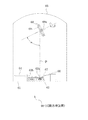
具体的には、例えば図3に示す揺動蒸着装置60によって、上述の条件を満たす位相差補償素子が作製される。揺動蒸着装置60は、ベースプレート61にターレット式に回転する材料ホルダ62が設けられており、その中に蒸着材料63a,63bが収容される。真空槽65を真空引きした後、電子銃66から電子ビーム67を蒸着材料63aに照射し、蒸着材料63aを溶融し、蒸発させ真空蒸着を行う。このとき、シャッタ64の開閉によって真空蒸着の開始及び中止を制御することができる。また、材料ホルダ62を回転させることによって、蒸着材料63a,63bを蒸着源として選択することができるようになっている。
Specifically, for example, a phase difference compensation element that satisfies the above-described conditions is manufactured by the swing vapor deposition apparatus 60 shown in FIG. In the oscillating vapor deposition apparatus 60, a
材料ホルダ62の上方に、斜めに配置された基板ホルダ68が設けられており、この基板ホルダ68にガラスなどからなる基板69が保持される。基板ホルダ68の支持面の法線は、蒸着材料63aから垂直にのばした線分Pに対して角度αだけ傾いて設けられている。したがって、基板69の蒸着面も線分Pに対して角度αだけ傾いて配置され、蒸着方向の極角は角度αに等しい。また、基板ホルダ68は、紙面と垂直な軸を中心に回転自在に設けられており、この基板ホルダ68の回転によって極角αが自在に調節される。
A
また、基板ホルダ68は、軸68aを中心に回転自在に設けられている。蒸着中に基板ホルダ68を、軸68aを中心に回転させることによって、一定の極角αに保ちながら、透明基板69の所定基準位置から見た相対的な蒸着材料63aの飛来方向の角度(以下、方位角)βを自在に変化させることができるようになっている。
The
このように構成される揺動蒸着装置60で、基板69の表面の法線を軸とした曲線軌道上で基板69を移動させ、方位角βを蒸着している最中に変化させることで、前述の各条件を満たす位相差補償素子が作製される。蒸着中の方位角βの変化様態は、所定の角度範囲内での振動的な往復回転(以下、揺動)であることが好ましい。また、この揺動の角度範囲は、0度より大きく90度以下の範囲であることが好ましく、10度以上であることがより好ましい。さらに、10度以上60度以下であることが特に好ましい。
With the oscillating vapor deposition apparatus 60 configured in this way, the
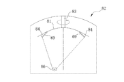
上述の揺動蒸着装置60によって斜方蒸着を行うと、図4に示すように、基板69から見た蒸着源71は、基板69の表面の法線に平行な回転軸72を中心として円弧軌道73上を遥動する。このとき、蒸着源71は、基板69に対して一定の極角αを保ったまま、所定の方位角βの範囲で揺動する。すなわち、基板69に対する蒸着材料の極角αを略一定に保ちながら、方位角βの範囲内で連続的に蒸着材料が飛来し、堆積する。この過程によって、主屈折率n2の方向にも広がりを持って堆積が進行し、その結果、主屈折率n2の値が大きくなる。また、揺動の速さが堆積の速さと比べて十分に速くなるようにすれば、作製される斜方蒸着膜の物理的な微細構造はS型に歪むことなく、主屈折率n1の方向が蒸着源の位置を時間平均した方向(平均の蒸着方位)L1に傾斜した構造となる。
When oblique vapor deposition is performed by the oscillating vapor deposition apparatus 60 described above, the vapor deposition source 71 viewed from the
なお、蒸着装置の形態は上述の揺動蒸着装置60のように蒸着中に基板を揺動させるものに限らない。例えば、図5に示すように、一方向に回転する台座81に複数の基板69を配置する回転蒸着装置82は、前述の条件を満たす位相差補償素子(二軸性複屈折体)の作製に適している。この回転蒸着装置82は、台座81、回転軸83、基板ホルダ84、蒸着源86などからなる。台座81は、蒸着源86の方向から見て凹状に湾曲した形状となっており、その凹面に複数の基板ホルダ84が設けられている。また、蒸着源86は、台座81の回転軸83から所定距離を隔てて配置されている。すなわち、蒸着源86は、台座81の回転中心から偏心した位置に設けられている。
In addition, the form of the vapor deposition apparatus is not limited to that which swings the substrate during vapor deposition like the above-described rocking vapor deposition apparatus 60. For example, as shown in FIG. 5, a
このように構成される回転蒸着装置82によって、基板69を回転軸83のまわりに回転させながら蒸着を行うと、図6に示すように、基板69からみた蒸着源86は円軌道87上を所定方向に周回する。したがって、極角αが所定角度範囲内で振動的に変化するとともに、方位角βも所定角度範囲内で振動的に変化する。このように、所定範囲内の異なる方位角βから連続的に蒸着材料を堆積させることによって、主屈折率n2の方向にも広がりを持って堆積が進行し、その結果、主屈折率n2の値が大きくなる。また、台座81の回転の速さが蒸着材料の堆積する速さと比べて十分に速くなるようにすれば、作製される斜方蒸着膜の物理的な微細構造はらせん型に歪むことなく、主屈折率n3の方向が蒸着源86の位置を時間平均した方向(平均の蒸着方位)L2に傾斜した構造となる。
When vapor deposition is performed by rotating the
なお、上述の回転蒸着装置82によって斜方蒸着を行う場合には、台座81と蒸着源86との間に、基板69が台座81によって回転される軌道の一部分を蒸着源86から遮蔽することが好ましい。例えば、所定サイズの単スリットが設けられた遮蔽板を台座81と蒸着源86との間に配置すれば良い。このように、基板69の回転軌道の一部を蒸着源86から遮蔽すると、蒸着材料が基板69に飛来する極角αと方位角βの分布が変わる。したがって、遮蔽する部分を調節することで、主屈折率n1と主屈折率n3の基板表面に対する傾斜角度及びT値を制御することができる。
When oblique vapor deposition is performed by the above-described rotary
[液晶素子に対する位相差補償素子の配置]
上述のように作製される位相差補償素子の液晶素子に対する配置は、必要な視野角範囲内の光線に対して液晶素子の傾斜配向成分の方向と位相差補償素子の正面位相差の遅相軸とが略直交するように配置する。さらに、基板平面の法線から傾斜した光線に対する液晶素子の傾斜配向成分による位相差と位相差補償素子による位相差の増減が逆になる方向に配置する。
[Arrangement of retardation compensation element for liquid crystal element]
The arrangement of the phase difference compensation element manufactured as described above with respect to the liquid crystal element is such that the direction of the tilt alignment component of the liquid crystal element and the slow axis of the front phase difference of the phase difference compensation element with respect to the light beam within the required viewing angle range And are arranged so as to be substantially orthogonal. Further, the phase difference due to the tilt alignment component of the liquid crystal element and the phase difference increase / decrease by the phase difference compensation element with respect to the light ray inclined from the normal line of the substrate plane are arranged in opposite directions.
こうした配置によって所定視野角範囲内の光線に生じる位相差の視野角依存性を補償され、液晶素子の視野角が拡大され、液晶プロジェクタのコントラストが改善される。 With such an arrangement, the viewing angle dependency of the phase difference generated in the light beam within the predetermined viewing angle range is compensated, the viewing angle of the liquid crystal element is expanded, and the contrast of the liquid crystal projector is improved.
すなわち、例えば、図5に示すように、液晶素子96内で傾斜配向成分の液晶分子が傾斜する方向と、位相差補償素子40の屈折率楕円体41の傾斜方向とは、z軸の正方向を挟んでy軸方向の正方向と負の方向を向くように配置する。このとき、傾斜配向成分による液晶素子の正面位相差の遅相軸方向L3はy軸に平行な方向となり、かつ、位相差補償素子の正面位相差の遅相軸方向L4はx軸に平行な方向となる。したがって、傾斜配向成分の正面位相差の遅相軸方向と位相差補償素子の正面位相差の遅相軸方向は垂直となる。
That is, for example, as shown in FIG. 5, the direction in which the liquid crystal molecules of the tilt alignment component are tilted in the liquid crystal element 96 and the tilt direction of the refractive index ellipsoid 41 of the phase
具体的に、例えばTN液晶素子に前述のように作製される位相差補償素子を適用する場合、TN液晶素子の上下面の2箇所にある傾斜配向成分の各々に応じて、2層の位相差補償素子を配置する。すなわち、前述のように作製される位相差補償素子の正面位相差の遅相軸方向が互いに直交するように2層の位相差補償素子を配置する。このとき、2層の位相差補償素子を別個に作成する必要はなく、同一の透明基板上の両面又は片面に斜方蒸着膜を作製しても良い。なお、TN液晶素子に対して1層の位相差補償素子だけを用いる場合にも、一方の傾斜配向成分による位相差が補償されるので、ある程度のコントラスト改善効果が得られる。 Specifically, for example, when the phase difference compensation element manufactured as described above is applied to a TN liquid crystal element, two layers of phase differences are provided in accordance with each of the tilt alignment components at two locations on the upper and lower surfaces of the TN liquid crystal element. A compensation element is arranged. That is, the two-layer phase difference compensation elements are arranged so that the slow axis directions of the front phase differences of the phase difference compensation elements manufactured as described above are orthogonal to each other. At this time, it is not necessary to separately prepare two layers of phase difference compensation elements, and oblique vapor deposition films may be formed on both sides or one side of the same transparent substrate. Even when only one phase difference compensation element is used for the TN liquid crystal element, the phase difference due to one tilt alignment component is compensated, so that a certain degree of contrast improvement effect can be obtained.
また、VAN液晶素子は、液晶分子が基板の法線方向から5度程度プレチルトしていることによって所定視野角範囲内の光線に位相差が生じる。したがって、上述のように作製した1層の位相差補償素子を、液晶分子がプレチルトしている方向と位相差補償素子の正面位相差の遅相軸方向とが垂直になるように配置する。 Further, in the VAN liquid crystal element, a phase difference occurs in light rays within a predetermined viewing angle range because liquid crystal molecules are pretilted by about 5 degrees from the normal direction of the substrate. Therefore, the single layer retardation compensation element manufactured as described above is arranged so that the direction in which the liquid crystal molecules are pretilted and the slow axis direction of the front retardation of the retardation compensation element are perpendicular to each other.
同様に、OCB液晶素子に対しては、2層の位相差補償素子を、各々の屈折率楕円体の傾斜方向が逆向きで、かつ、正面位相差の遅相軸が互いに平衡となるように重ねて配置すればよい。また、ECB液晶に対しては、電圧が印加されている状態の液晶層内に傾斜配向成分が2箇所あるが、配向方向が平行なので、位相差補償素子は1層設けるだけでよい。 Similarly, for the OCB liquid crystal element, a two-layer retardation compensation element is used so that the inclination directions of the refractive index ellipsoids are opposite to each other and the slow axes of the front phase differences are balanced with each other. What is necessary is just to arrange | position. In addition, for ECB liquid crystal, there are two inclined alignment components in the liquid crystal layer to which a voltage is applied. However, since the alignment directions are parallel, only one phase difference compensation element needs to be provided.
なお、何れの液晶素子に位相差補償素子を配置する場合にも、負のCプレートを併せて配置しても良い。この負のCプレートは、有機ポリマーでも薄膜で構成した構造性複屈折体でも良い。 In addition, in the case where the phase difference compensation element is arranged in any liquid crystal element, a negative C plate may be arranged together. The negative C plate may be an organic polymer or a structural birefringent body formed of a thin film.
何れにしても、上述のように作製した位相差補償素子を、偏光板と液晶素子の間に少なくとも1枚配置することによって、液晶プロジェクタがスクリーンに投影する画像のコントラストは飛躍的に向上する。このことを以下に実施例を挙げて説明する。 In any case, by disposing at least one retardation compensation element manufactured as described above between the polarizing plate and the liquid crystal element, the contrast of the image projected on the screen by the liquid crystal projector is dramatically improved. This will be described below with reference to examples.
[実施例1]
蒸着源と基板との距離が600mmとなる揺動蒸着装置60で、極角αが70度となるようにホウ珪酸ガラスからなる基板を配置し、この基板上に毎秒0.2nmの成膜速度で物理膜厚が1.5μmとなるまでZrO2とTiO2とからなる組成物を斜方蒸着した。このとき、基板は±30度の範囲で1分間に10回の速さで揺動させた。このように作製した斜方蒸着膜の断面をSEMで観察したところ、基板法線から35度の傾斜角度の節理状微細構造が観察されたが、基板を揺動させたことに対応する周期の微細構造は認められなかった。
[Example 1]
A substrate made of borosilicate glass is arranged so that the polar angle α is 70 degrees in an oscillating vapor deposition apparatus 60 in which the distance between the vapor deposition source and the substrate is 600 mm, and a film formation rate of 0.2 nm per second is formed on this substrate. Then, a composition composed of ZrO 2 and TiO 2 was obliquely evaporated until the physical film thickness became 1.5 μm. At this time, the substrate was swung at a speed of 10 times per minute within a range of ± 30 degrees. When the cross section of the obliquely deposited film thus prepared was observed with an SEM, a joint-like microstructure with an inclination angle of 35 degrees from the substrate normal was observed, but the period corresponding to the oscillation of the substrate was observed. No microstructure was observed.
こうして作製された位相差補償素子は、波長550nmの光に対して正面位相差が65nmであり、主屈折率n1=1.760、主屈折率n2=1.730、主屈折率n3=1.640、T=0.75であり、基板表面の法線に対する屈折率楕円体の傾斜角度θは24であった。また、この位相差補償素子の正面位相差の遅相軸は、基板から見た蒸着源の回転の中心方向を基板に正射影した方向と直角を成す方位であった。 The phase difference compensator thus fabricated has a front phase difference of 65 nm with respect to light having a wavelength of 550 nm, a main refractive index n1 = 1.760, a main refractive index n2 = 1.730, and a main refractive index n3 = 1. 640, T = 0.75, and the inclination angle θ of the refractive index ellipsoid with respect to the normal of the substrate surface was 24. Further, the slow axis of the front phase difference of this phase difference compensation element was an orientation perpendicular to the direction in which the central direction of rotation of the vapor deposition source viewed from the substrate was orthogonally projected onto the substrate.
[実施例2]
膜厚を2.0μmとしたほかは、実施例1と同じ条件で位相差補償素子を作製した。この位相差補償素子は、波長550nmの光に対して正面位相差10nmであり、主屈折率n1=1.800、主屈折率n2=1.782、主屈折率n3=1.743、T=0.68であり、基板表面の法線に対する屈折率楕円体の傾斜角度θは24度であった。また、正面位相差の遅相軸もまた、実施例1と同様に、基板から見た蒸着源の回転中心方向を基板に正射影した方向と直角を成す方位であった。さらに、この位相差補償素子を、VAN液晶素子を搭載する液晶プロジェクタに1層適用すると、位相差補償素子を用いない場合に800:1であった投影画像のコントラストが1500:1に向上した。
[Example 2]
A retardation compensation element was produced under the same conditions as in Example 1 except that the film thickness was 2.0 μm. This phase difference compensation element has a front phase difference of 10 nm with respect to light having a wavelength of 550 nm, a main refractive index n1 = 1.800, a main refractive index n2 = 1.782, a main refractive index n3 = 1.743, and T = It was 0.68, and the inclination angle θ of the refractive index ellipsoid with respect to the normal of the substrate surface was 24 degrees. Further, the slow axis of the front phase difference was also an orientation perpendicular to the direction in which the rotation center direction of the vapor deposition source viewed from the substrate was orthogonally projected onto the substrate, as in Example 1. Further, when one layer of this phase difference compensation element is applied to a liquid crystal projector equipped with a VAN liquid crystal element, the contrast of the projected image, which was 800: 1 when the phase difference compensation element was not used, was improved to 1500: 1.
[実施例3]
五酸化タンタルをガラスからなる基板上に、毎秒0.2nmの成膜速度で物理膜厚が1.0μmとなるように斜方蒸着膜を作製した。この位相差補償素子の作製には、回転蒸着装置82を用いた。使用した回転蒸着装置82の蒸着源と台座の回転軸との距離は400mmであり、基板は回転軸から450mmで高さ1000mmの位置に設置した。また、台座は1分間に10回の速さで回転させ、この回転の間に、蒸着方向の極角αは72度から35度まで変化し、方位角βは±23度の範囲で変化した。
[Example 3]
An oblique vapor deposition film was formed on a glass substrate of tantalum pentoxide so that the physical film thickness was 1.0 μm at a film formation rate of 0.2 nm per second. A
こうして作製された位相差補償素子は、波長550nmの光に対して正面位相差は50nmであり、主屈折率n1=1.800、主屈折率n2=1.782、主屈折率n3=1.744、T=0.68であり、基板表面の法線に対する屈折率楕円体の傾斜角度θは24度であった。また、この位相差補償素子の正面位相差の遅相軸は、基板から見た蒸着源の回転の中心方向を基板に正射影した方向と直角を成す方位であった。こうして作製した位相差補償素子を、TN液晶素子を搭載する液晶プロジェクタに2層適用すると、位相差補償素子を用いない場合に450:1であった投影画像のコントラストが1000:1に向上した。 The phase difference compensation element thus fabricated has a front phase difference of 50 nm with respect to light having a wavelength of 550 nm, a main refractive index n1 = 1.800, a main refractive index n2 = 1.782, a main refractive index n3 = 1. 744, T = 0.68, and the inclination angle θ of the refractive index ellipsoid with respect to the normal line of the substrate surface was 24 degrees. Further, the slow axis of the front phase difference of this phase difference compensation element was an orientation perpendicular to the direction in which the central direction of rotation of the vapor deposition source viewed from the substrate was orthogonally projected onto the substrate. When two layers of the phase difference compensation element thus manufactured are applied to a liquid crystal projector equipped with a TN liquid crystal element, the contrast of the projected image, which was 450: 1 when the phase difference compensation element is not used, is improved to 1000: 1.
上述の実施例から明らかなように、本発明の位相差補償素子によれば、液晶素子の傾斜配向成分による位相差を適切に補償し、液晶プロジェクタのコントラストを改善することができる。また、本発明の位相差補償素子は、無機材料の斜表蒸着膜からなるから、耐久性に富み、低コストに作製することができる。 As is apparent from the above-described embodiments, according to the phase difference compensating element of the present invention, the phase difference due to the tilt alignment component of the liquid crystal element can be appropriately compensated, and the contrast of the liquid crystal projector can be improved. In addition, since the retardation compensation element of the present invention is composed of an obliquely deposited film of an inorganic material, it has excellent durability and can be manufactured at low cost.
20 TN液晶素子
21 液晶分子
22 垂直配向成分
23,24 傾斜配向成分
40 位相差補償素子(二軸性複屈折体)
41 屈折率楕円体
60 蒸着装置
α 極角
β 方位角
θ 屈折率楕円体の傾斜角度
L1,L2 平均の蒸着方位
L3,L4 遅相軸
20 TN liquid crystal element 21 Liquid crystal molecule 22 Vertical alignment component 23, 24
41 Index ellipsoid 60 Vapor deposition device α Polar angle β Azimuth angle θ Refractive index ellipsoid tilt angle L1, L2 Average deposition orientation L3, L4 Slow axis
Claims (6)
前記主屈折率n1の方向が前記基板表面の法線から10度以上50度以下の角度をなして傾斜し、
各主屈折率の値が n1>n3 かつ (n2−n3)/(n1−n3)>0.3 なる関係を満たし、
前記基板表面の法線方向から測定した位相差の遅相軸が、前記主屈折率n2の方向と略平行であることを特徴とする二軸性複屈折体。 It consists of an inorganic material deposited on the substrate by oblique vapor deposition. The main refractive index n1 is determined in a plane including the vapor deposition direction and the normal of the substrate surface, and the main refractive index n2 is determined in a direction parallel to the substrate surface. In a biaxial birefringent body having a main refractive index n3 determined in a direction perpendicular to the refractive indexes n1 and n2,
The direction of the main refractive index n1 is inclined at an angle of 10 degrees to 50 degrees from the normal line of the substrate surface,
Each main refractive index value satisfies the relationship of n1> n3 and (n2-n3) / (n1-n3)> 0.3,
A biaxial birefringent body, wherein a slow axis of a phase difference measured from a normal direction of the substrate surface is substantially parallel to a direction of the main refractive index n2.
前記基板に対して蒸着材料が基板に飛来する方向の方位角を、所定の角度振幅の範囲内で振動的に変化させながら蒸着することを特徴とする二軸性複屈折体の製造方法。 In a method for producing a biaxial birefringent body in which an inorganic material is deposited on a substrate by oblique vapor deposition,
A method for producing a biaxial birefringent body, wherein vapor deposition is performed while oscillatingly changing an azimuth angle in a direction in which a vapor deposition material comes to the substrate with respect to the substrate within a range of a predetermined angular amplitude.
Priority Applications (7)
| Application Number | Priority Date | Filing Date | Title |
|---|---|---|---|
| JP2007245921A JP2009075459A (en) | 2007-09-21 | 2007-09-21 | Method for manufacturing biaxial birefringent material, biaxial birefringent material and liquid crystal projector |
| US12/679,240 US8605241B2 (en) | 2007-09-21 | 2008-09-18 | Biaxial birefringent component, liquid crystal projector, and method for manufacturing biaxial birefringent component |
| CN200880107754XA CN101802663B (en) | 2007-09-21 | 2008-09-18 | Biaxial birefringent component, liquid crystal projector, and method for manufacturing biaxial birefringent component |
| PCT/JP2008/067360 WO2009038218A1 (en) | 2007-09-21 | 2008-09-18 | Biaxial birefringent component, liquid crystal projector, and method for manufacturing biaxial birefringent component |
| EP08832696.2A EP2191307B1 (en) | 2007-09-21 | 2008-09-18 | Biaxial birefringent component, liquid crystal projector, and method for manufacturing biaxial birefringent component |
| KR1020107005966A KR20100071995A (en) | 2007-09-21 | 2008-09-18 | Biaxial birefringent component, liquid crystal projector, and method for manufacturing biaxial birefringent component |
| TW097135924A TWI443427B (en) | 2007-09-21 | 2008-09-19 | Method for manufacturing biaxial birefringent component |
Applications Claiming Priority (1)
| Application Number | Priority Date | Filing Date | Title |
|---|---|---|---|
| JP2007245921A JP2009075459A (en) | 2007-09-21 | 2007-09-21 | Method for manufacturing biaxial birefringent material, biaxial birefringent material and liquid crystal projector |
Related Child Applications (1)
| Application Number | Title | Priority Date | Filing Date |
|---|---|---|---|
| JP2010273726A Division JP5318079B2 (en) | 2010-12-08 | 2010-12-08 | Method for producing biaxial birefringent body |
Publications (2)
| Publication Number | Publication Date |
|---|---|
| JP2009075459A true JP2009075459A (en) | 2009-04-09 |
| JP2009075459A5 JP2009075459A5 (en) | 2010-04-08 |
Family
ID=40468025
Family Applications (1)
| Application Number | Title | Priority Date | Filing Date |
|---|---|---|---|
| JP2007245921A Abandoned JP2009075459A (en) | 2007-09-21 | 2007-09-21 | Method for manufacturing biaxial birefringent material, biaxial birefringent material and liquid crystal projector |
Country Status (7)
| Country | Link |
|---|---|
| US (1) | US8605241B2 (en) |
| EP (1) | EP2191307B1 (en) |
| JP (1) | JP2009075459A (en) |
| KR (1) | KR20100071995A (en) |
| CN (1) | CN101802663B (en) |
| TW (1) | TWI443427B (en) |
| WO (1) | WO2009038218A1 (en) |
Cited By (7)
| Publication number | Priority date | Publication date | Assignee | Title |
|---|---|---|---|---|
| JP2009161843A (en) * | 2008-01-10 | 2009-07-23 | Fujinon Corp | Work supporting member, optical element, phase difference element, and polarization beam splitter |
| JP2011076030A (en) * | 2009-10-02 | 2011-04-14 | Seiko Epson Corp | Liquid crystal device, electronic device, and projection type display device |
| JP2014170247A (en) * | 2014-06-23 | 2014-09-18 | Seiko Epson Corp | Liquid crystal device and electronic apparatus |
| JP2017049594A (en) * | 2016-10-17 | 2017-03-09 | デクセリアルズ株式会社 | Phase difference element and manufacturing method of the same, liquid crystal display, and projection type image display unit |
| WO2019230559A1 (en) * | 2018-05-31 | 2019-12-05 | デクセリアルズ株式会社 | Phase difference compensating element, liquid crystal display device, and projection-type image display device |
| WO2022004712A1 (en) * | 2020-06-30 | 2022-01-06 | 富士フイルム株式会社 | Retarder, liquid-crystal projector, and contrast adjustment method |
| US11947221B2 (en) | 2021-12-28 | 2024-04-02 | Fujifilm Corporation | Phase difference compensation element, liquid crystal display element, and liquid crystal projector |
Families Citing this family (2)
| Publication number | Priority date | Publication date | Assignee | Title |
|---|---|---|---|---|
| TWI826607B (en) * | 2018-12-07 | 2023-12-21 | 美商思娜公司 | Display system, spatial light modulator system and method of forming display system |
| JP2022021962A (en) * | 2020-07-23 | 2022-02-03 | セイコーエプソン株式会社 | Liquid crystal device and electronic apparatus |
Citations (1)
| Publication number | Priority date | Publication date | Assignee | Title |
|---|---|---|---|---|
| JP2006505014A (en) * | 2002-10-30 | 2006-02-09 | カラーリンク・インコーポレイテッド | Multiple obliquely oriented plate compensators for multiple projection display systems |
Family Cites Families (25)
| Publication number | Priority date | Publication date | Assignee | Title |
|---|---|---|---|---|
| US4529741A (en) | 1984-10-26 | 1985-07-16 | Dow Corning Corporation | Nonslumping foamable polyorganosiloxane compositions containing silica and fibers |
| US5196953A (en) * | 1991-11-01 | 1993-03-23 | Rockwell International Corporation | Compensator for liquid crystal display, having two types of layers with different refractive indices alternating |
| JPH05132768A (en) | 1991-11-13 | 1993-05-28 | Ricoh Co Ltd | Double refraction sheet and its manufacture |
| US5638197A (en) * | 1994-04-04 | 1997-06-10 | Rockwell International Corp. | Inorganic thin film compensator for improved gray scale performance in twisted nematic liquid crystal displays and method of making |
| US5504603A (en) * | 1994-04-04 | 1996-04-02 | Rockwell International Corporation | Optical compensator for improved gray scale performance in liquid crystal display |
| US5619352A (en) * | 1994-04-04 | 1997-04-08 | Rockwell International Corporation | LCD splay/twist compensator having varying tilt and /or azimuthal angles for improved gray scale performance |
| US5557434A (en) * | 1994-09-30 | 1996-09-17 | Rockwell International | Optical compensator including an o-plate for super-twist nematic liquid crystal display |
| JPH09296265A (en) | 1996-05-08 | 1997-11-18 | Matsushita Electric Ind Co Ltd | Production of oblique vapor-deposited coating film |
| JPH10330940A (en) | 1997-06-04 | 1998-12-15 | Oki Electric Ind Co Ltd | Vapor deposition apparatus for multilayered metallic wiring |
| JPH11263861A (en) | 1997-11-28 | 1999-09-28 | Sumitomo Chem Co Ltd | Preparation of phase difference film |
| JP4009044B2 (en) | 1999-10-08 | 2007-11-14 | リコー光学株式会社 | Thin-film birefringent element and method and apparatus for manufacturing the same |
| JP2002014345A (en) | 2000-06-28 | 2002-01-18 | Sony Corp | Projection liquid crystal display device |
| JP2002031782A (en) | 2000-07-18 | 2002-01-31 | Seiko Epson Corp | Projector |
| JP2002131750A (en) | 2000-10-27 | 2002-05-09 | Matsushita Electric Ind Co Ltd | Projection type display device |
| KR100852224B1 (en) * | 2000-12-28 | 2008-08-13 | 하야시 텔렘프 가부시끼가이샤 | Retardation film and process for producing the same |
| US6824838B2 (en) * | 2002-03-11 | 2004-11-30 | Fuji Photo Film Co., Ltd. | Retarders and circular polarizers |
| WO2004010712A1 (en) * | 2002-07-19 | 2004-01-29 | Fuji Photo Film Co., Ltd. | Liquid crystal projector, liquid crystal device and substrate for liquid crystal device |
| JP2004102200A (en) | 2002-07-19 | 2004-04-02 | Fuji Photo Film Co Ltd | Liquid crystal projector |
| EP1825305A4 (en) * | 2004-12-15 | 2010-07-07 | Fujifilm Corp | Phase difference compensator, light modurating system, liquid crystal display and liquid crystal projector |
| JP2006171328A (en) * | 2004-12-15 | 2006-06-29 | Fuji Photo Film Co Ltd | Phase difference compensation element, optical modulation system, liquid crystal display device, and liquid crystal projector |
| JP2006292784A (en) | 2005-04-05 | 2006-10-26 | Matsushita Electric Ind Co Ltd | Oblique vapor deposition film element |
| JP2007017485A (en) * | 2005-07-05 | 2007-01-25 | Fujifilm Holdings Corp | Liquid crystal display device and liquid crystal projector |
| JP2007086406A (en) | 2005-09-22 | 2007-04-05 | Fujifilm Corp | Liquid crystal display device, optically anisotropic object and its manufacturing method |
| JP2008242411A (en) * | 2006-09-27 | 2008-10-09 | Seiko Epson Corp | Deposition apparatus and deposition method, and method of manufacturing liquid crystal device |
| JP5098375B2 (en) * | 2007-03-12 | 2012-12-12 | セイコーエプソン株式会社 | Manufacturing method of liquid crystal device |
-
2007
- 2007-09-21 JP JP2007245921A patent/JP2009075459A/en not_active Abandoned
-
2008
- 2008-09-18 US US12/679,240 patent/US8605241B2/en active Active
- 2008-09-18 EP EP08832696.2A patent/EP2191307B1/en active Active
- 2008-09-18 KR KR1020107005966A patent/KR20100071995A/en not_active Application Discontinuation
- 2008-09-18 CN CN200880107754XA patent/CN101802663B/en active Active
- 2008-09-18 WO PCT/JP2008/067360 patent/WO2009038218A1/en active Application Filing
- 2008-09-19 TW TW097135924A patent/TWI443427B/en not_active IP Right Cessation
Patent Citations (1)
| Publication number | Priority date | Publication date | Assignee | Title |
|---|---|---|---|---|
| JP2006505014A (en) * | 2002-10-30 | 2006-02-09 | カラーリンク・インコーポレイテッド | Multiple obliquely oriented plate compensators for multiple projection display systems |
Cited By (11)
| Publication number | Priority date | Publication date | Assignee | Title |
|---|---|---|---|---|
| JP2009161843A (en) * | 2008-01-10 | 2009-07-23 | Fujinon Corp | Work supporting member, optical element, phase difference element, and polarization beam splitter |
| JP2011076030A (en) * | 2009-10-02 | 2011-04-14 | Seiko Epson Corp | Liquid crystal device, electronic device, and projection type display device |
| JP2014170247A (en) * | 2014-06-23 | 2014-09-18 | Seiko Epson Corp | Liquid crystal device and electronic apparatus |
| JP2017049594A (en) * | 2016-10-17 | 2017-03-09 | デクセリアルズ株式会社 | Phase difference element and manufacturing method of the same, liquid crystal display, and projection type image display unit |
| WO2019230559A1 (en) * | 2018-05-31 | 2019-12-05 | デクセリアルズ株式会社 | Phase difference compensating element, liquid crystal display device, and projection-type image display device |
| JP2019211494A (en) * | 2018-05-31 | 2019-12-12 | デクセリアルズ株式会社 | Phase difference compensation element, liquid crystal display device, and projection image display device |
| US11281049B2 (en) | 2018-05-31 | 2022-03-22 | Dexerials Corporation | Phase difference compensating element, liquid crystal display device, and projection-type image display device |
| JP7236225B2 (en) | 2018-05-31 | 2023-03-09 | デクセリアルズ株式会社 | Phase difference compensation element, liquid crystal display device and projection type image display device |
| WO2022004712A1 (en) * | 2020-06-30 | 2022-01-06 | 富士フイルム株式会社 | Retarder, liquid-crystal projector, and contrast adjustment method |
| US11899315B2 (en) | 2020-06-30 | 2024-02-13 | Fujifilm Corporation | Phase difference plate, liquid crystal projector, and contrast adjustment method |
| US11947221B2 (en) | 2021-12-28 | 2024-04-02 | Fujifilm Corporation | Phase difference compensation element, liquid crystal display element, and liquid crystal projector |
Also Published As
| Publication number | Publication date |
|---|---|
| TW200921215A (en) | 2009-05-16 |
| EP2191307A1 (en) | 2010-06-02 |
| WO2009038218A1 (en) | 2009-03-26 |
| CN101802663A (en) | 2010-08-11 |
| KR20100071995A (en) | 2010-06-29 |
| US20100231835A1 (en) | 2010-09-16 |
| TWI443427B (en) | 2014-07-01 |
| EP2191307A4 (en) | 2012-11-21 |
| US8605241B2 (en) | 2013-12-10 |
| EP2191307B1 (en) | 2019-09-11 |
| CN101802663B (en) | 2013-01-23 |
Similar Documents
| Publication | Publication Date | Title |
|---|---|---|
| JP2009075459A (en) | Method for manufacturing biaxial birefringent material, biaxial birefringent material and liquid crystal projector | |
| TWI427374B (en) | Retardation compensation element, van liquid crystal display device, and liquid crystal projector | |
| TWI393963B (en) | Retardation compensation element, liquid crystal display device, and liquid crystal projector | |
| TWI639860B (en) | Transmittance-variable film and eyewear using the same | |
| EP2096487B1 (en) | Reflective type liquid crystal display element and reflective type liquid crystal projector | |
| KR101824952B1 (en) | Liquid crystal display and optical compensation method therefor | |
| JP5318079B2 (en) | Method for producing biaxial birefringent body | |
| JP2006119444A (en) | Retardation compensation element and liquid crystal device using the same | |
| JP2009505141A (en) | Contrast enhancement for liquid crystal projection systems | |
| JP2007264065A (en) | Phase difference compensating element | |
| JP2006171328A (en) | Phase difference compensation element, optical modulation system, liquid crystal display device, and liquid crystal projector | |
| JP5552728B2 (en) | Liquid crystal device, projector, optical compensation method for liquid crystal device, and retardation plate | |
| JP2007086406A (en) | Liquid crystal display device, optically anisotropic object and its manufacturing method | |
| JP2009145862A5 (en) | ||
| JP2007011208A (en) | Fresnel substrate sheet, fresnel lens sheet, transmission-type screen, rear projection type display device | |
| JP2005172984A (en) | Reflective liquid crystal projector | |
| US11947221B2 (en) | Phase difference compensation element, liquid crystal display element, and liquid crystal projector | |
| JP2009075460A (en) | Phase-shift compensation device, liquid crystal display device, and projector | |
| JP2006350323A (en) | Liquid crystal display device and manufacturing method of liquid crystal display device | |
| TW200944890A (en) | Liquid crystal device, projector, and optical compensation method of liquid crystal device | |
| JP2004046069A (en) | Reflection type liquid crystal projector | |
| JP2018060089A (en) | Optical system and image projection device |
Legal Events
| Date | Code | Title | Description |
|---|---|---|---|
| A521 | Written amendment |
Free format text: JAPANESE INTERMEDIATE CODE: A523 Effective date: 20100217 |
|
| A871 | Explanation of circumstances concerning accelerated examination |
Free format text: JAPANESE INTERMEDIATE CODE: A871 Effective date: 20100217 |
|
| A621 | Written request for application examination |
Free format text: JAPANESE INTERMEDIATE CODE: A621 Effective date: 20100218 |
|
| A975 | Report on accelerated examination |
Free format text: JAPANESE INTERMEDIATE CODE: A971005 Effective date: 20100405 |
|
| A131 | Notification of reasons for refusal |
Free format text: JAPANESE INTERMEDIATE CODE: A131 Effective date: 20100407 |
|
| A521 | Written amendment |
Free format text: JAPANESE INTERMEDIATE CODE: A523 Effective date: 20100607 |
|
| A02 | Decision of refusal |
Free format text: JAPANESE INTERMEDIATE CODE: A02 Effective date: 20100908 |
|
| A762 | Written abandonment of application |
Free format text: JAPANESE INTERMEDIATE CODE: A762 Effective date: 20101208 |