JP2008519969A - Microfluidic device with minimization of ohmic resistance - Google Patents
Microfluidic device with minimization of ohmic resistance Download PDFInfo
- Publication number
- JP2008519969A JP2008519969A JP2007540593A JP2007540593A JP2008519969A JP 2008519969 A JP2008519969 A JP 2008519969A JP 2007540593 A JP2007540593 A JP 2007540593A JP 2007540593 A JP2007540593 A JP 2007540593A JP 2008519969 A JP2008519969 A JP 2008519969A
- Authority
- JP
- Japan
- Prior art keywords
- microfluidic device
- microstructure
- electrochemical
- electrochemical microfluidic
- electrode
- Prior art date
- Legal status (The legal status is an assumption and is not a legal conclusion. Google has not performed a legal analysis and makes no representation as to the accuracy of the status listed.)
- Pending
Links
Images


Classifications
-
- G—PHYSICS
- G01—MEASURING; TESTING
- G01N—INVESTIGATING OR ANALYSING MATERIALS BY DETERMINING THEIR CHEMICAL OR PHYSICAL PROPERTIES
- G01N33/00—Investigating or analysing materials by specific methods not covered by groups G01N1/00 - G01N31/00
- G01N33/48—Biological material, e.g. blood, urine; Haemocytometers
- G01N33/50—Chemical analysis of biological material, e.g. blood, urine; Testing involving biospecific ligand binding methods; Immunological testing
- G01N33/53—Immunoassay; Biospecific binding assay; Materials therefor
- G01N33/543—Immunoassay; Biospecific binding assay; Materials therefor with an insoluble carrier for immobilising immunochemicals
- G01N33/54366—Apparatus specially adapted for solid-phase testing
- G01N33/54373—Apparatus specially adapted for solid-phase testing involving physiochemical end-point determination, e.g. wave-guides, FETS, gratings
- G01N33/5438—Electrodes
-
- B—PERFORMING OPERATIONS; TRANSPORTING
- B01—PHYSICAL OR CHEMICAL PROCESSES OR APPARATUS IN GENERAL
- B01L—CHEMICAL OR PHYSICAL LABORATORY APPARATUS FOR GENERAL USE
- B01L3/00—Containers or dishes for laboratory use, e.g. laboratory glassware; Droppers
- B01L3/50—Containers for the purpose of retaining a material to be analysed, e.g. test tubes
- B01L3/502—Containers for the purpose of retaining a material to be analysed, e.g. test tubes with fluid transport, e.g. in multi-compartment structures
- B01L3/5027—Containers for the purpose of retaining a material to be analysed, e.g. test tubes with fluid transport, e.g. in multi-compartment structures by integrated microfluidic structures, i.e. dimensions of channels and chambers are such that surface tension forces are important, e.g. lab-on-a-chip
- B01L3/502707—Containers for the purpose of retaining a material to be analysed, e.g. test tubes with fluid transport, e.g. in multi-compartment structures by integrated microfluidic structures, i.e. dimensions of channels and chambers are such that surface tension forces are important, e.g. lab-on-a-chip characterised by the manufacture of the container or its components
-
- C—CHEMISTRY; METALLURGY
- C12—BIOCHEMISTRY; BEER; SPIRITS; WINE; VINEGAR; MICROBIOLOGY; ENZYMOLOGY; MUTATION OR GENETIC ENGINEERING
- C12Q—MEASURING OR TESTING PROCESSES INVOLVING ENZYMES, NUCLEIC ACIDS OR MICROORGANISMS; COMPOSITIONS OR TEST PAPERS THEREFOR; PROCESSES OF PREPARING SUCH COMPOSITIONS; CONDITION-RESPONSIVE CONTROL IN MICROBIOLOGICAL OR ENZYMOLOGICAL PROCESSES
- C12Q1/00—Measuring or testing processes involving enzymes, nucleic acids or microorganisms; Compositions therefor; Processes of preparing such compositions
- C12Q1/001—Enzyme electrodes
-
- B—PERFORMING OPERATIONS; TRANSPORTING
- B01—PHYSICAL OR CHEMICAL PROCESSES OR APPARATUS IN GENERAL
- B01L—CHEMICAL OR PHYSICAL LABORATORY APPARATUS FOR GENERAL USE
- B01L2300/00—Additional constructional details
- B01L2300/06—Auxiliary integrated devices, integrated components
- B01L2300/0627—Sensor or part of a sensor is integrated
- B01L2300/0645—Electrodes
-
- B—PERFORMING OPERATIONS; TRANSPORTING
- B01—PHYSICAL OR CHEMICAL PROCESSES OR APPARATUS IN GENERAL
- B01L—CHEMICAL OR PHYSICAL LABORATORY APPARATUS FOR GENERAL USE
- B01L2300/00—Additional constructional details
- B01L2300/08—Geometry, shape and general structure
- B01L2300/0809—Geometry, shape and general structure rectangular shaped
- B01L2300/0825—Test strips
-
- B—PERFORMING OPERATIONS; TRANSPORTING
- B01—PHYSICAL OR CHEMICAL PROCESSES OR APPARATUS IN GENERAL
- B01L—CHEMICAL OR PHYSICAL LABORATORY APPARATUS FOR GENERAL USE
- B01L2400/00—Moving or stopping fluids
- B01L2400/04—Moving fluids with specific forces or mechanical means
- B01L2400/0403—Moving fluids with specific forces or mechanical means specific forces
- B01L2400/0406—Moving fluids with specific forces or mechanical means specific forces capillary forces
-
- Y—GENERAL TAGGING OF NEW TECHNOLOGICAL DEVELOPMENTS; GENERAL TAGGING OF CROSS-SECTIONAL TECHNOLOGIES SPANNING OVER SEVERAL SECTIONS OF THE IPC; TECHNICAL SUBJECTS COVERED BY FORMER USPC CROSS-REFERENCE ART COLLECTIONS [XRACs] AND DIGESTS
- Y10—TECHNICAL SUBJECTS COVERED BY FORMER USPC
- Y10T—TECHNICAL SUBJECTS COVERED BY FORMER US CLASSIFICATION
- Y10T29/00—Metal working
- Y10T29/53—Means to assemble or disassemble
- Y10T29/5313—Means to assemble electrical device
- Y10T29/532—Conductor
- Y10T29/53204—Electrode
Landscapes
- Chemical & Material Sciences (AREA)
- Health & Medical Sciences (AREA)
- Life Sciences & Earth Sciences (AREA)
- Immunology (AREA)
- Engineering & Computer Science (AREA)
- General Health & Medical Sciences (AREA)
- Hematology (AREA)
- Analytical Chemistry (AREA)
- Organic Chemistry (AREA)
- Molecular Biology (AREA)
- Biochemistry (AREA)
- Wood Science & Technology (AREA)
- Zoology (AREA)
- Urology & Nephrology (AREA)
- Physics & Mathematics (AREA)
- Microbiology (AREA)
- Biomedical Technology (AREA)
- Biotechnology (AREA)
- Proteomics, Peptides & Aminoacids (AREA)
- Chemical Kinetics & Catalysis (AREA)
- Dispersion Chemistry (AREA)
- Clinical Laboratory Science (AREA)
- Pathology (AREA)
- Biophysics (AREA)
- General Physics & Mathematics (AREA)
- Cell Biology (AREA)
- Medicinal Chemistry (AREA)
- Food Science & Technology (AREA)
- Bioinformatics & Cheminformatics (AREA)
- General Engineering & Computer Science (AREA)
- Genetics & Genomics (AREA)
- Physical Or Chemical Processes And Apparatus (AREA)
- Apparatus Associated With Microorganisms And Enzymes (AREA)
Abstract
電気化学マイクロ流体装置であって、導電手段(7)が一体化されマイクロ構造内のオーム抵抗を低減するマイクロチャンネル(1)のような一又は複数のマイクロ構造、そしてそれによって、特に大電流密度が含まれる場合に、電気化学的測定を改善する。導電手段は対抗電極として接続可能でありかつ作用電極(4)で生じる反応生成物を再生するために使用されることも可能である。導電手段のような電気化学マイクロ流体装置を加工する方法も開示される。本発明は小容積で検知が行われるあらゆる電気化学センサーを適用するところで特に使用可能である。
【選択図】図1Electrochemical microfluidic device, one or more micro-structures such as micro-channel (1) in which the conductive means (7) are integrated and reduce the ohmic resistance in the micro-structure, and thereby a particularly high current density To improve electrochemical measurements. The conducting means can be connected as a counter electrode and can also be used to regenerate the reaction product produced at the working electrode (4). A method of processing an electrochemical microfluidic device, such as a conductive means, is also disclosed. The present invention is particularly applicable where any electrochemical sensor that senses in small volumes is applied.
[Selection] Figure 1
Description
分析装置の小型化は二つの理由により分析化学におけるトレンドとなっており、その理由とは:単一の分析に要する時間を低減すること及び試料/廃棄物の寸法を小さくすることである。マイクロ流体装置の製造及び発展しつつある検定のためにこの装置が使用されることにおいて、多くの成果がここ数年にわたって見られる。 Analyzer miniaturization has become a trend in analytical chemistry for two reasons: reducing the time required for a single analysis and reducing the size of the sample / waste. Many achievements have been seen over the last few years in the use of this device for the manufacture and development of microfluidic devices.
分析システムの小型化のひとつのボトルネックは、マイクロ流体装置の小容積に存する少量の分子の検知下限を確保することである。光学、質量スペクトル又は電気化学検知を含む、種々の検知手段は、かなり高濃度の検体を検知するためには首尾良く実施されてきた。例えば、多くのマイクロシステムは、マイクロ流体装置におけるグルコースの検知のために存在する。例えばTherasenseが開発したシステムがあり、これはわずか0.3μLの毛細管血における電量検知の遂行を可能にする。大きなダイナミックレンジを確保する一方で低濃度を検知することは、検知方法の最適化だけでなくマイクロ流体装置の配置の最適化も必要とする。本発明は、酸化還元活性分子の低濃度の検知を可能にする特定の方法及び関連する装置(特に酵素及び免疫検定(免疫学的検定)に適用される)を目的とする。 One bottleneck in the downsizing of analytical systems is to ensure a lower detection limit for small quantities of molecules in the small volume of microfluidic devices. Various detection means, including optical, mass spectrum or electrochemical detection, have been successfully implemented to detect very high concentrations of analytes. For example, many microsystems exist for the detection of glucose in microfluidic devices. For example, there is a system developed by Therasense, which makes it possible to perform coulometric detection in as little as 0.3 μL of capillary blood. Detecting low concentrations while ensuring a large dynamic range requires not only optimization of the detection method, but also optimization of the arrangement of the microfluidic device. The present invention is directed to specific methods and associated devices (particularly applied to enzymes and immunoassays) that allow detection of low concentrations of redox active molecules.
本発明は電気化学マイクロ流体装置及びマイクロ構造における電気化学的検知を最適化する方法に関係する。(そして好ましくは、マイクロチャンネル又はマイクロチャンネルのネットワークに関係する。)この装置の本質的な特徴はマイクロ構造のオーム抵抗を最小化することである。マイクロ構造のオーム抵抗(またはさらにはインピーダンス)の最小化は、電気化学的検知及び特に電気的測定の改善を可能にする、というのはオーム抵抗を補償するために適用する過電位も最小化され得るからであり、これは電気信号の品質の改善を可能にする。 The present invention relates to electrochemical microfluidic devices and methods for optimizing electrochemical sensing in microstructures. (And preferably relates to a microchannel or a network of microchannels.) An essential feature of this device is to minimize the ohmic resistance of the microstructure. Minimizing the ohmic resistance (or even impedance) of the microstructure allows for improved electrochemical sensing and in particular electrical measurements, since the overpotential applied to compensate the ohmic resistance is also minimized. This makes it possible to improve the quality of the electrical signal.
本発明の目的の一つは従ってマイクロ流体装置における電気化学的な検知を最適化することである。マイクロ流体装置における電気化学検知は、小容積の酸化還元活性分子の検知のための魅力的な解決策として既に示されてきた。この技術は、例えば、分離後の検知手段として又は酵素若しくは免疫学的検定分析のために使用可能である。マイクロ流体システムの制約の一つは、マイクロ構造の典型的な寸法が電流の伝導に対して極めて好ましくないことである。実際に、例えばマイクロ構造が、長さ(L)が一又は数cmの典型的な寸法を有しそして直径(d)が数十μmである管状毛細管からなる場合、たとえ溶液の抵抗率(ρ)がかなり低くとも、そのオーム抵抗(R)は高く、式1のオームの法則によって表現される: One object of the present invention is therefore to optimize electrochemical sensing in microfluidic devices. Electrochemical sensing in microfluidic devices has already been shown as an attractive solution for the detection of small volumes of redox active molecules. This technique can be used, for example, as a detection means after separation or for enzyme or immunoassay analysis. One limitation of microfluidic systems is that the typical dimensions of the microstructure are highly undesirable for current conduction. In fact, for example, if the microstructure consists of a tubular capillary with a typical dimension of length (L) of one or several centimeters and a diameter (d) of several tens of micrometers, even if the resistivity of the solution (ρ ) Is quite low, its ohmic resistance (R) is high and is expressed by the Ohm's law of Equation 1:
R=ρL/A 式1
ここで、Aは管状毛細管の断面積であって、A=πd2/4である
R = ρL / A Equation 1
Here, A is a sectional area of the tubular capillaries is A = πd 2/4
例として、毛細管の半径が20μmであり且つ溶液を運ぶ毛細管の長さが1cmであるとき、係数L/Aは8x106cm−1に等しい。100mMのリン酸塩溶液の場合、このチャンネルに沿って小電流密度のみ流れることができるように、そのようなマイクロチャンネルに沿った抵抗はかねてから106Ωである。 As an example, when the radius of the capillary is 20 μm and the length of the capillary carrying the solution is 1 cm, the coefficient L / A is equal to 8 × 10 6 cm −1 . In the case of a 100 mM phosphate solution, the resistance along such a microchannel has always been 10 6 Ω so that only a small current density can flow along this channel.
マイクロ流体装置に存在する大きな抵抗は電気的な用途に対して重大な欠点である。実際に、この抵抗は応答を誤って伝えることがあり、このオーム抵抗による電圧降下を補償するためのフィードバック電圧を必要とするか又は大きな信号が正確に測定されるのを妨げる。このような電気化学的用途の場合、及び特に、電気化学的バイオセンサーの場合、低減した抵抗を持つマイクロ流体装置を有することは従って大きな利点となる。 The large resistance present in microfluidic devices is a serious drawback for electrical applications. In practice, this resistance can mislead the response, requiring a feedback voltage to compensate for the voltage drop due to this ohmic resistance, or preventing large signals from being accurately measured. For such electrochemical applications, and particularly for electrochemical biosensors, having a microfluidic device with reduced resistance is therefore a major advantage.
我々の発明では、このマイクロ構造の寸法は上記の例(このcm範囲のチャンネルの長さ及び数十μmのチャンネル直径)の寸法と同程度の大きさである。しかしながら、導電手段は、チャンネルの一点から別の点まで電気が流れるようにマイクロチャンネルの全体に沿って配置されるか又はマイクロ構造の一部に配置される。この場合、電流はチャンネルを通じたイオン電流によってのみ流れるわけではなく、この導電手段を通じても流れる。 In our invention, the dimensions of this microstructure are as large as the dimensions of the above example (channel length in this cm range and channel diameter of tens of micrometers). However, the conducting means is arranged along the entire microchannel or part of the microstructure so that electricity flows from one point of the channel to another. In this case, the current flows not only by the ion current through the channel, but also through this conducting means.
上述したのと同等の寸法のマイクロチャンネルを有するマイクロ構造において導電手段を有する場合と有さない場合に行った実験は、オーム抵抗(又は「iR降下」)がない場合に流れ得る電流強度がマイクロ構造が導電手段を含まない場合でより大きくなることを示した。ある場合には、導電手段は逆反応がチャンネル内部で起こるように対抗電極として接続されることが可能であり、そしてそれゆえにこの反応生成物の再生が作用電極で生じる。 Experiments conducted with and without conductive means in a microstructure with a microchannel of the same dimensions as described above show that the current intensity that can flow in the absence of ohmic resistance (or “iR drop”) is micro It has been shown that the structure is larger when it does not include conductive means. In some cases, the conducting means can be connected as a counter electrode so that the reverse reaction occurs inside the channel, and therefore regeneration of this reaction product occurs at the working electrode.
以下でさらに詳細に示されるように、導電手段が接続されておらず、従って検知の役に立つ電極を組合せたもの(以降「電極システム」としても言及される)の一部ではない場合でさえ、優れた電気化学的応答が得られることが可能であるということも証拠にあげられる。明瞭にするために、二電極システムは作用電極及び擬似参照電極だけ含みそして、三電極システムは作用電極、対抗電極及び参照電極を含む。本発明では、マイクロ流体装置は導電手段を含み、この導電手段は二電極システム又は三電極システムに加えられて存在してもよく、そしてこの導電手段はその後これらの電極のいずれかとも接続されない。このような場合で、マイクロ流体装置は溶液で満たされるとき、接点が電極の組合せと導電手段との間で生じ、このようにして広範囲の電気回路の一部となる。本発明において、導電手段はそれ自体で対抗電極又はみせかけの参照電極を構成し、そしてその後電極の組合せの一部となる。両方の配置において、この導電手段は適用され非常に低抵抗の電流経路を提供し、非常に小さい断面積のマイクロ構造の場合ですら、マイクロ構造の広範囲の抵抗は最小限にされる。以下でさらに詳細に記載されるように、このマイクロ構造の抵抗は、導電手段が直接に接続されていないときでさえ、このように低減されるようである。 As will be shown in more detail below, even if the conductive means are not connected and are therefore not part of a combination of electrodes useful for sensing (hereinafter also referred to as "electrode system") The evidence also shows that it is possible to obtain an electrochemical response. For clarity, the two-electrode system includes only a working electrode and a pseudo reference electrode, and the three-electrode system includes a working electrode, a counter electrode, and a reference electrode. In the present invention, the microfluidic device includes conductive means, which may be present in addition to the two-electrode system or the three-electrode system, and the conductive means is not subsequently connected to any of these electrodes. In such cases, when the microfluidic device is filled with a solution, a contact occurs between the electrode combination and the conductive means, thus becoming part of a wide range of electrical circuits. In the present invention, the conducting means itself constitutes a counter electrode or a fake reference electrode and then becomes part of the electrode combination. In both arrangements, this conductive means is applied to provide a very low resistance current path, and even in the case of very small cross-sectional microstructures, the extensive resistance of the microstructure is minimized. As described in further detail below, the resistance of this microstructure appears to be reduced in this way even when the conductive means are not directly connected.
この現象は、マイクロシステムにおける電気化学検知信号の動揺を防ぐために、非常に興味深いものであり、そしてマイクロ構造に沿った導電手段の存在がシステムを作り、このシステムは概略的に二つの平行な電極(一つはマイクロ構造の小さな寸法の結果である大きな抵抗、Rm、及び導電手段として役に立つ導電材料の非常に低い抵抗性のせいで非常に低い抵抗、Rc)によって表される。そして導電手段が電気化学検知回路に接続されない場合でさえ、これらの抵抗は同時に稼働する。従って、この結果としての広範囲の抵抗、Rg、はおおよそRcに等しく、導電手段が一種の抵抗のバイパスとして作用することになり、これは電流にとってより有利なルートを提供する。システムの非常に低い広範囲の抵抗のために、(大電流が存在するときでさえ)適用される電位はしたがってマイクロ構造全体に沿ってほぼ一定に維持される。導電手段の集積は従ってiR降下によるみせかけの電気化学信号を妨げ、そして本発明は、マイクロセンサーシステムにおける電気化学検知のために得ることが可能である、信号の品質を改善する強力な手段をこのようにして提供する。 This phenomenon is very interesting to prevent perturbation of the electrochemical sensing signal in the microsystem, and the presence of conductive means along the microstructure makes the system, which is roughly two parallel electrodes (One is the very low resistance, Rc, due to the large resistance, Rm, and the very low resistance of the conductive material that serves as the conductive means, which is the result of the small dimensions of the microstructure). And even when the conductive means is not connected to the electrochemical sensing circuit, these resistors work simultaneously. The resulting wide range of resistance, Rg, is therefore approximately equal to Rc, and the conductive means acts as a kind of resistance bypass, which provides a more advantageous route for the current. Because of the very low wide range resistance of the system, the applied potential is therefore maintained nearly constant along the entire microstructure (even when large currents are present). The integration of the conductive means thus prevents spurious electrochemical signals due to iR drops, and the present invention provides a powerful means to improve the signal quality that can be obtained for electrochemical sensing in microsensor systems. To provide.
本発明の装置では電気泳動は不可能であることに着目すべきである、というのは導電手段がマイクロ構造に沿ってほぼ一定の電位を維持するからであり、この結果ほとんど電界勾配は発生せず、したがって電気浸透さらに電気泳動分離を妨げることもない。 It should be noted that electrophoresis is not possible with the device of the present invention because the conducting means maintains a substantially constant potential along the microstructure, resulting in almost no electric field gradient. Therefore, it does not interfere with electroosmosis or electrophoretic separation.
本発明はマイクロ流体装置を提供し、マイクロ流体装置は少なくとも一つのマイクロ構造を含み、マイクロ構造は一または一連の作用電極を含み、さらにマイクロ構造内部で一体化した導電手段をマイクロ構造内部のオーム抵抗を低減するようなやり方で含む。オーム抵抗の低減は特に小さな寸法の(例えばマイクロチャンネル)のセンサーで又は大電流密度が使用されるときに必要とされる、なぜならばこのオーム抵抗が電気化学的に測定可能な信号を妨害するからである。本発明のマイクロ流体装置は低減したオーム抵抗を有する電気化学センサーを対象としており、それによって電気化学応答の改善を可能にしている。 The present invention provides a microfluidic device, wherein the microfluidic device includes at least one microstructure, the microstructure includes one or a series of working electrodes, and a conductive means integrated within the microstructure is an ohm within the microstructure. Including in a manner that reduces resistance. Reduction of ohmic resistance is required especially with small size (eg microchannel) sensors or when high current densities are used, since this ohmic resistance interferes with electrochemically measurable signals. It is. The microfluidic device of the present invention is directed to an electrochemical sensor having reduced ohmic resistance, thereby enabling improved electrochemical response.
本発明の一実施態様において、導電手段は対抗電極として接続され、これは検知すべき検体を再生するための還元又は酸化(又は「酸化還元」)の間に都合良く使用されることができる。別の実施態様では、この伝導手段は外部の電気計器(例えばポテンシオスタット、電源、等)に接続されていない。従って、このような構成では、この導電手段は電極ではなく(というのは、これが接続されていないから)、高い電気抵抗でできた経路(例えばマイクロチャンネルの溶液)のまわりに電流を導くためのマイクロ流体装置に加えた道具にすぎず、それによってこのシステムの全体の抵抗を低減することが可能になる。このような導電手段はマイクロ構造のオーム抵抗を低減させることが可能であり、したがって酸化還元反応の際に得ることができる信号を最適化する。例えば、全体の長さに沿った導電手段を含むマイクロチャンネル及びマイクロチャンネルの入口又は出口に置かれた対抗電極又は擬似参照電極を伴い、一方で作用電極はマイクロチャンネルの壁部分の中で一体化されているとき、この導電手段は(接続されていないときであっても)マイクロチャンネルに沿って、従って入口又は出口に置かれた対抗電極又は擬似参照電極から離れた作用電極までの距離にわたって、電流を運ぶことが可能であり、このことが抵抗を最小にし、従ってこのような装置で得ることができる電気化学信号を最適化することを可能にする。ここで本発明の装置は必ずしも参照電極又は擬似参照電極を含まないということが強調されるべきである。実際に、この参照電極又は擬似参照電極は他の機器の一部によってもたらされてもよく、従ってマイクロ流体装置の一体化部分ではない。例えば、参照電極又は擬似参照電極は銀/塩化銀ワイヤーであってもよく、これはマイクロ構造の入口又は出口の貯留槽に置かれているか又は溶液をマイクロ流体装置に分注するのに役立つ手段(例えば注射器)に置かれており、そのやり方はこの参照電極又は擬似参照電極が電気化学検知の間に検体溶液と接触するようなやり方である。これは、本発明のマイクロ流体装置が使い捨てであって従って各分析後又は境界の明確な一連の試験の後に廃棄されることが予定されており、一方でマイクロ流体装置が新しいものに取り替えられても参照電極又は擬似参照電極が残っていることが予定される場合に、達成可能である。 In one embodiment of the invention, the conducting means is connected as a counter electrode, which can be conveniently used during reduction or oxidation (or “redox”) to regenerate the analyte to be detected. In another embodiment, the conducting means is not connected to an external electrical meter (eg, potentiostat, power source, etc.). Thus, in such a configuration, the conducting means is not an electrode (since it is not connected), but is used to direct current around a path of high electrical resistance (eg a solution in a microchannel). It is just a tool added to the microfluidic device, which makes it possible to reduce the overall resistance of the system. Such conducting means can reduce the ohmic resistance of the microstructure and thus optimize the signal that can be obtained during the redox reaction. For example, with a microchannel containing conductive means along the entire length and a counter or pseudo reference electrode placed at the inlet or outlet of the microchannel, while the working electrode is integrated within the wall portion of the microchannel When done, this conducting means (even when not connected) is along the microchannel and thus over a distance from the counter electrode or pseudo reference electrode placed at the inlet or outlet to the working electrode. It is possible to carry an electric current, which minimizes the resistance and thus makes it possible to optimize the electrochemical signal that can be obtained with such a device. It should be emphasized here that the device according to the invention does not necessarily comprise a reference electrode or a pseudo-reference electrode. Indeed, this reference electrode or pseudo reference electrode may be provided by a part of other equipment and is therefore not an integral part of the microfluidic device. For example, the reference electrode or pseudo reference electrode may be a silver / silver chloride wire, which is placed in a reservoir at the microstructure inlet or outlet or a means to help dispense the solution into the microfluidic device (For example, a syringe), which is such that the reference electrode or pseudo reference electrode contacts the analyte solution during electrochemical sensing. This is due to the fact that the microfluidic device of the present invention is disposable and therefore will be discarded after each analysis or after a series of well-defined tests, while the microfluidic device is replaced with a new one. Can also be achieved if it is expected that a reference or pseudo reference electrode will remain.
本発明のさらなる態様はマイクロ流体装置を加工する方法を提供し、この方法は、マイクロ構造内のオーム抵抗を最小にするためにマイクロ構造に存在する溶液と接触するように導電手段を一体化することを含む。一実施態様において、導電手段は少なくとも一つのスルーホールを伴って形成され、スルーホールはマイクロ構造を支持(サポート)する基材にマイクロ構造を造るためのマスクとしての役目を果たし、そしてそこではマスクの周りでアンダーエッチングが実施されて導電手段がマイクロ流体装置に存在する溶液と接触可能となる。 A further aspect of the invention provides a method of processing a microfluidic device, which integrates a conductive means to contact a solution present in the microstructure to minimize ohmic resistance in the microstructure. Including that. In one embodiment, the conductive means is formed with at least one through hole, the through hole serving as a mask for creating the microstructure on a substrate that supports the microstructure, wherein the mask is Under-etching is performed around the conductive means so that the conductive means can come into contact with the solution present in the microfluidic device.
本発明の第三の態様は請求項49に記載された電気化学マイクロ流体装置の使用を提供することである。 A third aspect of the present invention is to provide the use of an electrochemical microfluidic device according to claim 49.
本発明の装置及び方法は電気化学センサー用途で都合良く使用されることができ、そして特に化学的及び/又は生物学的分析、例えば化合物の物理化学特性試験又は分析試験、例えば免疫学的分析法、酵素、イオン、DNA、ペプチド、オリゴヌクレオチド又は細胞分析法で都合良く使用されることができる。本発明は医学的診断、獣医試験、環境又は水の分析、品質管理、産業管理、薬剤調査、戦争用薬剤の検知、製造プロセスの監視、等において多くの用途を見つけることができる。 The apparatus and method of the present invention can be advantageously used in electrochemical sensor applications, and in particular chemical and / or biological analysis, such as physicochemical property testing or analytical testing of compounds, such as immunological analysis. Can be conveniently used in enzymes, ions, DNA, peptides, oligonucleotides or cell analysis. The present invention can find many applications in medical diagnostics, veterinary testing, environmental or water analysis, quality control, industrial management, drug research, war drug detection, manufacturing process monitoring, and the like.
本発明はこのようにしてマイクロ構造(概してマイクロチャンネル又はマイクロチャンネルのネットワーク)内のオーム抵抗を最小化することを可能にする一又は複数の導電手段を含むマイクロ流体装置を提供する。本発明のマイクロ流体装置はまた、前記導電手段に加えて、一又は複数の作用電極(好ましくはマイクロ電極)を含む。作用電極及び導電手段の両方が、それぞれ個々の作用電極と導電手段との間の距離を最短化するために、お互いに向き合うようなやり方でマイクロ構造の壁部分に一体化されてもよい。概して、参照電極又は擬似参照電極もまたマイクロ流体装置の部分であり(それがマイクロチャンネルである場合、マイクロ構造の入口及び/又は出口に置かれるのが好ましい)、そして一つ又は一連の対抗電極も、三電極モードにおいて電気化学検知を可能とするために、マイクロ流体装置の部分になり得る。 The present invention thus provides a microfluidic device comprising one or more conductive means that makes it possible to minimize the ohmic resistance in the microstructure (generally a microchannel or a network of microchannels). The microfluidic device of the present invention also includes one or more working electrodes (preferably microelectrodes) in addition to the conductive means. Both the working electrode and the conductive means may be integrated into the wall portion of the microstructure in such a way as to face each other in order to minimize the distance between each individual working electrode and the conductive means. In general, the reference electrode or pseudo-reference electrode is also part of the microfluidic device (preferably placed at the inlet and / or outlet of the microstructure if it is a microchannel) and one or a series of counter electrodes Can also be part of a microfluidic device to allow electrochemical sensing in the three-electrode mode.
マイクロ流体装置又はマイクロ構造の寸法及び形状に制約はなく、これらは任意の手段(例えば、限定はされないが、射出成形、エンボス、ポリマーキャスティング、ケイ素エッチング、UV Liga(リソグラフィ電気メッキ成型)、湿潤エッチング、乾燥エッチング)によって且つ任意の電気絶縁材料(例えば、ガラス、水晶、セラミック、ポリマー又はこれらの組合せ)において加工されることができる。一実施態様において、マイクロ流体装置は材料を組立てたもの及びしっかりした構造から構成される:例えばポリマーホイルでできたマイクロ流体センサーではマイクロ構造サポートとしての役目を果たしそこでは(プリント回路ボードシステムのように)種々の電極、導電手段並びに接続パッド及び接続トラックが存在することがあり、さらに例えばポリマー又はガラスでできた被覆層であって、これがマイクロ流体操作を可能にするためにマイクロ構造をシール又は被覆するのに役立つ。追加部分は別のポリマー材料から造ることができ、そして例えば入口及び/又は出口へのアクセスホール並びに追加的な貯留槽を含んでもよく、これは試料及び試薬の注入又は引き抜き及び/又は流体制御ユニットへの接続を可能にし、センサーの取り扱いを促進するために、これはまた完全なセンサー装置に剛性をもたらすこともでき又はマイクロ構造それ自体に比べれば比較的大きなサイズのマイクロ流体センサーカートリッジにすることができる。このような多構造及び多材料装置はピックアンドプレースアプローチによって都合良く加工することができ、ここではその被覆層を伴うマイクロ構造サポートがパネル又はボードから切り出され、このパネル又はボードは追加的部分(例えば射出成形構造)に正確に組み立てられる(例えば糊付けによって)前の一連のマイクロ構造を含み、追加部分は流体の及び/又は電気の接続のためのアクセスホールを有し且つ随意的に試料又は試薬貯留槽を有する(例えば以下の図15の例を参照)。さらに電気接続を確実にしまたは促進するために、又は(銀又は銀/塩化銀インクドットのような)参照電極を一体化するために、導電トラック及びパッドが造られてもよい。このようなマイクロ流体センサー装置を加工するために他のプロセスが使用されてもよく、例えばマイクロ構造サポート及び例えばアクセスホール及び/又は試薬貯留槽を提供するのに適したポリマー部分を伴う被覆層をオーバーモールドすることによって加工されてもよい。 There are no restrictions on the size and shape of the microfluidic device or microstructure, which can be by any means (for example, but not limited to, injection molding, embossing, polymer casting, silicon etching, UV Liga (lithographic electroplating), wet etching. , Dry etching) and in any electrically insulating material (eg, glass, quartz, ceramic, polymer, or combinations thereof). In one embodiment, the microfluidic device is composed of an assembled material and a rigid structure: for example, a microfluidic sensor made of polymer foil serves as a microstructural support (such as a printed circuit board system). There may be various electrodes, conductive means and connection pads and connection tracks, and also a coating layer, for example made of polymer or glass, which seals or seals the microstructure to allow microfluidic manipulation. Useful for coating. The additional part can be made from another polymer material and may include, for example, access holes to the inlet and / or outlet and additional reservoirs, which can be used to inject or withdraw samples and reagents and / or fluid control units This can also provide rigidity to the complete sensor device or make it a relatively large microfluidic sensor cartridge compared to the microstructure itself to allow connection to and facilitate sensor handling Can do. Such multi-structure and multi-material devices can be conveniently processed by a pick-and-place approach, in which the microstructure support with its covering layer is cut out of the panel or board, which is then added to an additional part ( Including a series of microstructures prior to being accurately assembled (e.g., by gluing), e.g., injection molded structures, with additional portions having access holes for fluid and / or electrical connections and optionally samples or reagents It has a storage tank (see, for example, the example of FIG. 15 below). In addition, conductive tracks and pads may be made to ensure or facilitate electrical connections or to integrate reference electrodes (such as silver or silver / silver chloride ink dots). Other processes may be used to fabricate such a microfluidic sensor device, such as a coating layer with a polymer portion suitable to provide, for example, a microstructure support and, for example, access holes and / or reagent reservoirs. It may be processed by overmolding.
作用電極は前記マイクロ流体装置に存在する流体の電気化学的特性の一つ又は複数を制御、監視及び/又は測定することに適合している。特に、これらの電極はアンペロメトリック、サイクリックボルタメトリック、クロノアンペロメトリック及び/又はインピーダンス測定に適合しており、そして本発明の装置は化学的及び/又は生物学的用途、例えば限定はされないが免疫学的、酵素、親和性、イオン、ペプチド、DNA、オリゴヌクレオチド又は細胞分析法、さらに物理化学試験、例えば溶解性、脂質親和性又は浸透性分析法又は酸化還元特性の測定において、都合良く使用されることが可能である。用途に応じて、このマイクロ構造はまた化学的及び/又は生物学的化合物で都合良く官能化されてもよい。最後まで、官能化基はマイクロ構造の内部表面で造られることが可能である(例えば化学的又は物理的手段によって)。例えばカルボキシル、アミノ、チオール又はフェノール基は、マイクロ構造表面を構成する材料を伴う化学反応によって又は電極又は導電手段としての役目を果たすものを伴う化学反応によって一体化されることができる。化学的及び/又は生物学的化合物はまたマイクロ構造の少なくとも一部で可逆的に又は不可逆的に、例えば限定はされないが吸着、イオン結合又は共有結合で固定化される。化学的及び/又は生物学的化合物はマイクロ構造壁の少なくとも一部に及び/又は一体化した作用電極及び導電手段に固定化されることができる。一実施態様において、本発明の装置は固定化した化合物を含まずに一体化した作用電極のみを維持することに適合させてもよく、すなわちこの装置は化学的及び/又は生物学的化合物を作用電極に接触することはなくマイクロ構造の壁に固定できることに適合し得る。最後まで、このマイクロ流体装置は、作用電極がマイクロ構造に埋め込まれるようなやり方で、都合良く加工可能である。このような凹みは疎水性に造られてもよく、及び/又は親水性溶液がこのマイクロ構造を通過し作用電極に接触することなくこの凹みを通過する適当な形状を有してもよく、これによって化学的又は生物学的材料を伴う官能化を防ぐ。このようなマイクロ流体装置では例えば、作用電極を濡らすことができる溶液(例えば試料、緩衝液、洗浄媒体、捕捉した分子の曝露)がマイクロ構造に導入されないかぎり、溶液が作用電極に接触しないやり方で、多工程分析が実施されることが可能である。マイクロ構造はそのような湿潤溶液で満たされているとき、例えばそれは埋め込まれた金の作用電極を有するポリイミドマイクロチャンネル中のTween緩衝剤のような界面活性剤を伴って達成され、その埋め込み部の疎水性は低減し、結果としてマイクロ構造が他のもの、親水性溶液でもよい、で満たされることでさらに作用電極を濡らすことになる。この湿潤溶液の導入は分析のあらゆる工程で行うことができ、作用電極がマイクロ構造に存在する溶液と接触していることが望まれるときであるかどうかによって決まる。例えば免疫学的試験のような多工程分析では、これらの多様な溶液と作用電極との間に全く接触させずそして検知の直前に湿潤溶液(これは例えば捕捉した検体を明らかにするのに役立つ酵素基材を含むことができる)を追加しないで、この分析法の全ての工程(望ましい検体の捕捉、洗浄、第二の抗体の培養及び追加の洗浄)を実施することが実際に有利である可能性がある。 The working electrode is adapted to control, monitor and / or measure one or more of the electrochemical properties of the fluid present in the microfluidic device. In particular, these electrodes are adapted for amperometric, cyclic voltammetric, chronoamperometric and / or impedance measurements, and the device of the present invention is not limited to chemical and / or biological applications such as Is useful in immunological, enzymatic, affinity, ion, peptide, DNA, oligonucleotide or cell analysis methods, as well as in physicochemical tests such as solubility, lipophilicity or permeability analysis methods or measurement of redox properties Can be used. Depending on the application, the microstructure may also be conveniently functionalized with chemical and / or biological compounds. To the end, functionalized groups can be created on the internal surface of the microstructure (eg, by chemical or physical means). For example, carboxyl, amino, thiol or phenol groups can be integrated by chemical reactions with the materials that make up the microstructured surface or by chemical reactions with those that serve as electrodes or conducting means. Chemical and / or biological compounds are also immobilized reversibly or irreversibly in at least part of the microstructure, such as, but not limited to, adsorption, ionic bonding or covalent bonding. Chemical and / or biological compounds can be immobilized on at least a part of the microstructure wall and / or on an integrated working electrode and conductive means. In one embodiment, the device of the present invention may be adapted to maintain only an integrated working electrode without the immobilized compound, i.e., the device may act on chemical and / or biological compounds. It can be adapted to be fixed to the wall of the microstructure without contacting the electrode. To the end, the microfluidic device can be conveniently processed in such a way that the working electrode is embedded in the microstructure. Such indentations may be made hydrophobic and / or have a suitable shape that allows the hydrophilic solution to pass through the indentations without passing through the microstructure and contacting the working electrode. Prevents functionalization with chemical or biological materials. In such microfluidic devices, for example, the solution does not contact the working electrode unless a solution that can wet the working electrode (eg, sample, buffer, wash medium, exposure of captured molecules) is introduced into the microstructure. A multi-step analysis can be performed. When the microstructure is filled with such a wetting solution, for example, it is achieved with a surfactant such as a Tween buffer in a polyimide microchannel with an embedded gold working electrode, Hydrophobicity is reduced and as a result, the working electrode is further wetted by filling the microstructure with another, which may be a hydrophilic solution. This introduction of the wetting solution can take place at any stage of the analysis and depends on whether it is desired that the working electrode is in contact with the solution present in the microstructure. In a multi-step analysis such as an immunological test, there is no contact between these various solutions and the working electrode and a wet solution just before detection (this serves for example to reveal captured analytes) It is practically advantageous to carry out all steps of this method (capturing the desired analyte, washing, culturing the second antibody and additional washing) without adding an enzyme substrate) there is a possibility.
別の実施態様において、本発明の装置は作用電極のみが化学的又は生物学的物質と官能化するやり方で製造されてもよい。これは例えば直接的に作用電極だけに付着することによって達成され得る。このようなプロセスは作用電極を例えばオリゴヌクレオチド、DNAストレイン又は細胞と官能化させるために仕様され得る。 In another embodiment, the device of the present invention may be manufactured in such a way that only the working electrode is functionalized with a chemical or biological substance. This can be accomplished, for example, by attaching directly to the working electrode only. Such a process can be specified to functionalize the working electrode with, for example, oligonucleotides, DNA strains or cells.
いくつかの実施態様において、乾燥した試薬もマイクロ流体装置を官能化させるために使用されてよく、そして官能化はまた望ましい化学的及び/又は生物学的実在物を含むビーズ、メンブレン又はフィルターを使用することによって達成され得る。 In some embodiments, dried reagents may also be used to functionalize the microfluidic device, and functionalization also uses beads, membranes or filters that contain the desired chemical and / or biological entities. Can be achieved.
一実施態様において、本発明のマイクロ流体装置はマイクロ構造の少なくとも一つの壁部に一体化されている少なくとも一つの作用電極(又は作用電極配列)及び一つの擬似参照電極(すなわち、一つの電極が参照電極と対抗電極の両方の役割を果たしている)を含む二電極システムであって;このような二電極構成において、作用電極及び擬似参照電極に加えて導電手段が存在しているが、電気化学検知のために役立つ二電極システムの部分にはならないように導電性手段は接続はされていない;この場合に、この擬似参照電極はマイクロ構造の外側で、入口及び/又は出口の近くで、且つプローブに溶液が接するようなやり方で都合良く置かれてもよい。導電手段のおかげで、抵抗はマイクロ構造に沿って劇的に減少し、それによって最適な電気化学操作及び検知が可能になり;導電手段が対抗電極として接続されることを必要としない事実は予想されていなかった、しかしこの事実は本発明の補助的な利点を構成する。 In one embodiment, the microfluidic device of the present invention comprises at least one working electrode (or working electrode array) and one pseudo reference electrode (ie, one electrode integrated into at least one wall of the microstructure). A two-electrode system comprising both a reference electrode and a counter electrode); in such a two-electrode configuration, there is a conducting means in addition to the working electrode and the pseudo-reference electrode, but the electrochemical The conductive means are not connected so that they are not part of a two-electrode system that serves for sensing; in this case, the pseudo-reference electrode is outside the microstructure, near the inlet and / or outlet, and It may be conveniently placed in such a way that the solution contacts the probe. Thanks to the conductive means, the resistance decreases dramatically along the microstructure, thereby allowing for optimal electrochemical manipulation and sensing; the fact that the conductive means does not need to be connected as a counter electrode is expected This fact has not been done, but constitutes an auxiliary advantage of the present invention.
別の実施態様において、本発明の装置は少なくとも一つの作用電極(又は作用電極配列)、少なくとも一つの参照電極及び少なくとも一つの導電手段を含む三電極システムを構成する。一実施態様において、この導電手段は直接に対抗電極としての役目を果たすことに適合することが可能である。別の実施態様において、導電手段は三電極システムの部分ではなく、それは電極に接続されず、そして装置は対抗電極としての役目を果たす少なくとも一つの追加的な電極をさらに含む。 In another embodiment, the apparatus of the invention constitutes a three-electrode system comprising at least one working electrode (or working electrode array), at least one reference electrode and at least one conducting means. In one embodiment, the conductive means can be adapted to serve directly as a counter electrode. In another embodiment, the conductive means is not part of a three-electrode system, it is not connected to an electrode, and the device further comprises at least one additional electrode that serves as a counter electrode.
或る実施態様において、本発明のマイクロ流体装置は導電手段をマイクロ構造の長さ全体に沿って含み、そして導電手段はマイクロ構造を都合良く取り囲むことができ且つマイクロ構造に存在する溶液と接触する伝導性材料でできたフリーズ(frieze:帯状の浮き彫りにしたようなもの)を形成する。 In certain embodiments, the microfluidic device of the present invention includes conducting means along the entire length of the microstructure, and the conducting means can conveniently surround the microstructure and contact the solution present in the microstructure. Forms a frieze made of conductive material (like a banded relief).
さらなる実施態様において、導電手段及び擬似参照電極も短絡されることが可能である。これは例えばマイクロ流体装置を提供することによって達成されることが可能であり、このマイクロ流体装置では導電手段が入口及び/又は出口を包み込むマイクロ構造の周りのフリーズを形成する伝導パッドであり且つ溶液と接触するやり方で参照電極又は擬似参照電極が入口及び/又は出口の外側の伝導パッドに単純に付着される。 In a further embodiment, the conductive means and the pseudo reference electrode can also be shorted. This can be achieved, for example, by providing a microfluidic device, in which the conductive means is a conductive pad that forms a freeze around the microstructure surrounding the inlet and / or outlet and the solution A reference electrode or pseudo reference electrode is simply attached to the conductive pad outside the inlet and / or outlet in a manner that contacts it.
本発明の用途のいくつかにおいて、作用電極で生じる反応の生成物を再生するために対抗電極が使用可能であり、これにより測定信号が増加しそれによってこの装置の分析感度を改善する。導電手段はこの目的のために都合良く使用されることが可能であり;このような場合、導電手段は対抗電極の役割及び、検知すべき化合物を再生する役割、及びマイクロ構造に沿った抵抗を最小にする役割の全てを果たす。 In some of the applications of the present invention, a counter electrode can be used to regenerate the product of the reaction occurring at the working electrode, thereby increasing the measurement signal and thereby improving the analytical sensitivity of the device. Conductive means can be conveniently used for this purpose; in such cases, the conductive means can act as a counter electrode, regenerate the compound to be sensed, and provide resistance along the microstructure. Play all the roles to minimize.
本発明のさらなる実施態様において、マイクロ流体装置は少なくとも一つの生物学的及び/又は化学的実在物を含んでもよい。このような生物学的及び/又は化学的部分はマイクロ構造の少なくとも一つの壁の少なくとも一部で物理吸着、共有結合、イオン結合又は単純に乾燥させることのいずれかによって固定されることが可能である。別の実施態様において、一又は複数の目標の試料分子を捕捉するため又は試料を洗浄若しくは脱塩するためにマイクロ流体装置もビーズ及び/又はメンブレン(これは例えばマイクロ構造の入口及び/又は出口に置かれることができる)を含むことがある。このようなビーズ又はメンブレンはまた一又は複数の生物学的及び/又は化学的実在物を含んでもよく、それらはこれらのタイプのサポートに固定され得る。 In a further embodiment of the invention, the microfluidic device may comprise at least one biological and / or chemical entity. Such biological and / or chemical moieties can be immobilized either by physisorption, covalent bonding, ionic bonding or simply drying on at least a portion of at least one wall of the microstructure. is there. In another embodiment, the microfluidic device may also bead and / or membrane (eg, at the inlet and / or outlet of the microstructure) to capture one or more target sample molecules or to wash or desalt the sample. Can be placed). Such beads or membranes may also contain one or more biological and / or chemical entities, which can be secured to these types of supports.
マイクロ構造の壁及び/又は一体化した電極若しくは導電手段はまた部分的に有機相(固化されているか又はされていない)で被覆されることが可能であり、この有機相は例えば電極の保護層として又は試料溶液と混合しない相として使用されることもでき且つ二つの不混和性溶液の間の界面でのイオン移動反応の測定のためにセットアップされることもできそして例えばイオンの投与のために使用されることもできる。 The microstructure wall and / or the integrated electrode or conducting means can also be partly coated with an organic phase (solidified or not), for example the protective layer of the electrode Or as a phase that does not mix with the sample solution and can be set up for the measurement of ion transfer reactions at the interface between two immiscible solutions and for example for the administration of ions It can also be used.
マイクロ流体装置は補助的な層によって取り囲まれることができ、この補助的な層は固化剤として使用されることができ及び/又は貯留槽(例えば試薬を蓄えること及び/又は溶液の洗浄のための貯留槽)、さらに流体の及び/又は電気的な接続のためのアクセスホール、又は他の機器と相互作用するためのガイドを含む。 The microfluidic device can be surrounded by an auxiliary layer, which can be used as a solidifying agent and / or a reservoir (eg for storing reagents and / or for washing solutions) Reservoirs), access holes for fluid and / or electrical connections, or guides for interacting with other equipment.
本発明のマイクロ流体装置では、マイクロ構造基材の又はこの被覆層の化学的及び/又は物理的性質における制約はない。この基材及び被覆層の各々は例えばポリマー(例えばポリイミド、ポリスチレン、ポリカーボネート、ポリエチレン、ポリエチレンテレフタレートラミネート、液晶ポリマーがあるが、これらに限定はされない)、ガラス、水晶、セラミック等から造られてもよい。本発明において、「基材」という用語は実際にはそこでマイクロ構造が加工され得る任意の材料を言及する。ある基材はポリマーホイルであって、1mm未満の厚みを有する。一実施態様において、被覆層はマイクロ流体操作(例えばマイクロチャンネルを用いる)が可能となるようにマイクロ構造をシールするのに役立ち、そしてこの被覆層はそこで一又は複数の電極が加工され得るマイクロ構造及び/又は伝導パッドを含んでもよい。同様に、「マイクロ構造」が概して少なくとも寸法を有し、それが1mm未満であれば、本発明のマイクロ流体装置の材料及び/又は性質における制約はなく、マイクロ構造の形状及び寸法においても制約はない。好ましい実施態様において、マイクロ流体装置は多重層体でもあり、少なくとも一つの組立物から構成されていて、その組立物はマイクロ構造基材、この装置のオーム抵抗を減らすのに役立つ電極及び/又は導電手段を形成する導電トラック、さらにマイクロ構造をシールするのに概して役立つ(これによってマイクロ流体操作が可能になる)被覆層からできている。さらに好ましい実施態様では、被覆層はポリマー層であり、これはマイクロ構造基材にラミネート加工又は糊付けされている。 In the microfluidic device of the present invention, there are no restrictions on the chemical and / or physical properties of the microstructure substrate or of this coating layer. Each of the substrate and the coating layer may be made of, for example, a polymer (for example, but not limited to polyimide, polystyrene, polycarbonate, polyethylene, polyethylene terephthalate laminate, liquid crystal polymer), glass, crystal, ceramic, and the like. . In the present invention, the term “substrate” actually refers to any material in which the microstructure can be processed. One substrate is a polymer foil and has a thickness of less than 1 mm. In one embodiment, the coating layer serves to seal the microstructure so that microfluidic manipulation (eg, using microchannels) is possible, and the coating layer can be used to process one or more electrodes. And / or a conductive pad. Similarly, if the “microstructure” generally has at least dimensions and is less than 1 mm, there are no restrictions on the materials and / or properties of the microfluidic device of the present invention, and no restrictions on the shape and dimensions of the microstructure. Absent. In a preferred embodiment, the microfluidic device is also multi-layered and consists of at least one assembly, which assembly is a microstructured substrate, electrodes and / or conductive that help reduce the ohmic resistance of the device. It consists of a conductive track that forms the means, and a covering layer that generally serves to seal the microstructure (which allows microfluidic manipulation). In a further preferred embodiment, the coating layer is a polymer layer, which is laminated or glued to the microstructure substrate.
導電手段のみならず電極は任意の導電材料で造られることができ、導電材料は例えば金属(例えば金、銀、プラチナ又は任意の不活性金属)又は金属組立物(例えば金、銀、プラチナまたはそれに類するもので被覆した銅(例えば電気メッキによる))、導電インク(例えばAg/AgClインク)又はゲル(例えば透過性ゲル)であるがこれらに限定はされない。 The electrodes as well as the conductive means can be made of any conductive material, for example a metal (eg gold, silver, platinum or any inert metal) or a metal assembly (eg gold, silver, platinum or it) Copper (e.g., by electroplating), conductive ink (e.g., Ag / AgCl ink) or gel (e.g., permeable gel) coated with similar materials, but not limited thereto.
マイクロ流体システムを加工するための本方法において、オーム抵抗は一又は複数の導電手段の存在のおかげで減少する。一実施態様において、本発明は一又は複数のマイクロ構造(好ましくはマイクロチャンネル)、マイクロ構造の少なくとも一つの壁の部分を画定する一又は複数の導電手段、及び前記マイクロ構造を被覆し及び/又はシールするための被覆層を有する基材を含む多重層体に特定の配列をもたらす。本発明の或るマイクロ流体装置では、単数又は複数のその導電手段が一又は複数の溝又は穴を含み、前記マイクロ構造が導電手段のその辺に被覆又はシールされる場合、この溝又は穴はマイクロ構造の部分である(図1参照)。 In the present method for processing microfluidic systems, the ohmic resistance is reduced thanks to the presence of one or more conductive means. In one embodiment, the present invention covers one or more microstructures (preferably microchannels), one or more conductive means defining at least one wall portion of the microstructures, and / or covers said microstructures A particular arrangement is provided in a multilayer body comprising a substrate having a covering layer for sealing. In one microfluidic device of the present invention, when the one or more conducting means includes one or more grooves or holes and the microstructure is coated or sealed on its sides of the conducting means, the grooves or holes are It is a part of the microstructure (see FIG. 1).
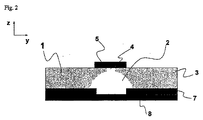
別の実施態様では、本発明はマイクロ構造の少なくとも一部に沿って単数又は複数のスルーホールを有する導電手段を含む電気化学マイクロ流体装置を製造する方法を提供し;被覆層を適用することによりマイクロ構造を被覆し又はシールすることによって、これらのホールがマイクロ構造に対して反対のホールのある側でシールされることが可能であり、この結果それらのホールはマイクロ構造の部分となり、このマイクロ構造はその後異なる材料(すなわち以下の図2の断面図で示されるような、マイクロ基材の部分、導電手段の材料の部分、及び被覆層の部分)を組み立てたものでできた少なくとも一つの壁の部分を有する。マイクロ構造が溶液で満たされるとき、このマイクロ構造内の溶液はその後自動的に導電手段と接触し、これはその形状及び種々の要素(以下の図1及び2の例で示されるマイクロ構造を構成しているもの)から容易に推測可能である。好ましい実施態様において、導電手段はこのようにしてスルーホールをもたらすことができ、そしてこの組立品はまた基材でのマイクロ構造の加工のためのパターン付けマスクとしての役目も都合良く果たすことができ;実際に、さらなるマイクロ加工のための望ましいパターンのスルーホールを形成するために(例えば従来のフォトレジスト付着及びそれに続いて光にあてること(例えば高解像コンピューター駆動プリンターで)によって)導電手段は例えばマイクロ構造基材に直接的に付着されてもよい。この導電手段はこのようにしてマスクを形成しそして、第二の加工工程で、エッチング又は研磨媒体に曝される基材の部分のおかげで、マイクロ構造は前記基材において(例えば、湿潤エッチング、化学エッチング、フォトアブレーション又はこれらの組合せにより)加工される。好ましい実施態様において、マイクロ加工工程は等位性エッチングプロセス(例えばプラズマ若しくはガスエッチング、又は任意の湿潤エッチングプロセス)から選択される、なぜならばこのような等位性プロセスは結果として三次元空間におけるエッチングをもたらし、したがってマスク側で材料の除去をもたらすからである。「アンダーエッチング」として知られるこの現象は、マイクロ構造が被覆又はシールされている(例えばラミネート加工層によって)ときであっても、導電手段がマイクロ構造に存在する溶液と接触することを確実にすることが可能である。 In another embodiment, the present invention provides a method of manufacturing an electrochemical microfluidic device that includes conductive means having one or more through holes along at least a portion of a microstructure; by applying a coating layer By covering or sealing the microstructure, these holes can be sealed on the side with the opposite hole to the microstructure, so that they become part of the microstructure and this micro The structure is then at least one wall made of different materials (i.e. part of the micro-base, part of the material of the conductive means and part of the covering layer as shown in the cross-sectional view of FIG. 2 below) It has a part. When the microstructure is filled with solution, the solution in this microstructure then automatically contacts the conductive means, which constitutes its shape and various elements (the microstructure shown in the examples of FIGS. 1 and 2 below). It can be easily guessed from what is). In a preferred embodiment, the conductive means can thus provide a through hole, and the assembly can also conveniently serve as a patterning mask for the fabrication of microstructures on the substrate. In fact, the conductive means is to form through holes in the desired pattern for further microfabrication (eg, by conventional photoresist deposition and subsequent exposure to light (eg, in a high resolution computer driven printer)) For example, it may be attached directly to the microstructure substrate. This conducting means thus forms a mask and, in the second processing step, thanks to the part of the substrate that is exposed to the etching or polishing medium, the microstructure is in said substrate (for example wet etching, Processed by chemical etching, photoablation or a combination thereof. In a preferred embodiment, the microfabrication step is selected from an isotropic etching process (eg plasma or gas etching, or any wet etching process), because such an isotropic process results in etching in a three-dimensional space. And thus the removal of material on the mask side. This phenomenon, known as “under-etching”, ensures that the conductive means is in contact with the solution present in the microstructure, even when the microstructure is coated or sealed (eg by a laminated layer). It is possible.
導電手段に及び他の電極と接続するパッドとトラックに望ましいデザインを与えるために、前記マイクロ構造の加工の後で、望ましくない導電部分(概してマイクロ加工プロセスのエッチング工程の間に曝されてはならない基材部分を保護するために使用される)が除去され得る(例えば化学エッチングによって)。電極は実際には、プロセス中に、マイクロ構造を閉じるため又はシールするために役立つ被覆層を加える前に、一体化されることも可能である。単数又は複数の作用電極が、例えばマイクロ構造の壁部で一体化されることが可能であり、そして好ましくは導電手段の反対にあるマイクロ構造基材の側から一体化されることが可能である。このような配置は実際にはマイクロ流体装置の全体の加工を促進するように、また一体化した作用電極と導電手段との間の距離を最小にするように選択されることが可能であり、これによりオーム抵抗を最小まで減らし、導電手段が対抗電極として使用され且つ検知すべき検体を再生するのに役立つ場合に拡散距離をほとんどもたらさない。 To provide the desired design for the conductive means and pads and tracks that connect to other electrodes, after the processing of the microstructure, it should not be exposed to unwanted conductive parts (generally during the etching step of the microfabrication process). Used to protect the substrate portion) can be removed (eg by chemical etching). In practice, the electrodes can also be integrated during the process before adding a coating layer that serves to close or seal the microstructure. The working electrode or electrodes can be integrated, for example at the wall of the microstructure, and can preferably be integrated from the side of the microstructure substrate that is opposite the conducting means. . Such an arrangement can actually be chosen to facilitate the overall processing of the microfluidic device and to minimize the distance between the integrated working electrode and the conducting means, This reduces the ohmic resistance to a minimum and provides little diffusion distance when the conductive means is used as a counter electrode and serves to regenerate the analyte to be detected.
マイクロ構造が官能化されなければならないとき(例えば、生物学的及び/又は化学的物質によって)、物理的(例えばプラズマ照射)及び/又は化学的手段(酸または塩基処理)によってマイクロ構造の壁の少なくとも一部を洗浄し又は修飾することが有利な場合がある。同様に、マイクロ構造の官能化は被覆層を加える前に都合よく実施されてもよい。 When the microstructure has to be functionalized (eg by biological and / or chemical substances), the walls of the microstructure can be physically (eg plasma irradiated) and / or by chemical means (acid or base treatment) It may be advantageous to wash or modify at least a portion. Similarly, the functionalization of the microstructure may be conveniently performed before applying the coating layer.
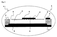
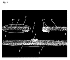
図1は本発明のマイクロ流体装置の一例の縦断面図であり、この装置は基材(3)(この基材は非伝導性ポリマー材料から優先的に選択されるが、限定はされない)に加工されたマイクロ構造(2)を含み、前記マイクロ構造は作用電極として単数又は複数のマイクロ電極又はマイクロ電極配列(4)を含み、概して外部ポテンシオスタットへ接続するための一つ又はいくつかの伝導性接続パッド(5)を提示し、さらにこの装置は導電手段(7)を含み、これ(7)はマイクロ構造基材の反対辺にあって、マイクロ構造と直接接触しており且つ本ケースでは作用マイクロ電極の前に置かれている。図1のマイクロ構造は被覆層(8)でシールされており、このカバー層はこの加工プロセスの最後に例えば糊付けされ又はラミネート加工される。図1の場合、マイクロ構造はアクセスホール(9)を含んだマイクロチャンネルであり、アクセスホールは入口及び出口としての役目を果たし、そして流体が導入(introduction)、送出し(uptake)、引戻し(withdrawal)又は分注(dispensing)されることを可能にする。 FIG. 1 is a longitudinal cross-sectional view of an example of a microfluidic device of the present invention, which is a substrate (3) (this substrate is preferentially selected from, but not limited to, a non-conductive polymer material). Comprising a fabricated microstructure (2), said microstructure comprising one or more microelectrodes or a microelectrode array (4) as working electrodes, generally one or several for connection to an external potentiostat A conductive connection pad (5) is presented and the device further comprises conductive means (7), which is on the opposite side of the microstructure substrate and is in direct contact with the microstructure and in this case Then it is placed in front of the working microelectrode. The microstructure of FIG. 1 is sealed with a covering layer (8), which is for example glued or laminated at the end of the processing process. In the case of FIG. 1, the microstructure is a microchannel containing an access hole (9), the access hole serves as inlet and outlet, and the fluid is introduced, uptake, and withdrawal. ) Or dispensed.
図1及び2での好ましい実施態様において、このマイクロ流体装置は少なくとも一つの電極(任意の適当な材料、例えば金属、から作られている)を伴うポリマーボディから作られている。このマイクロ流体装置(1)は基材(3)に組み込まれた少なくとも一つのマイクロ構造(2)から構成され、ここで前記構造は好ましくは500μm未満の断面積を画定し、前記マイクロ構造は一体化したマイクロ電極又はマイクロ電極配列(4)を有し、前記マイクロ電極又はマイクロ電極配列は伝導性パッド(5)によって支持(サポート)されている;このマイクロ流体装置は参照電極又は擬似参照電極も含み、この電極は例えば別の伝導性パッド(6)に付着された伝導性インク(例えばAg/AgClインク)から構成され、これは都合良くマイクロ構造の入口及び/又は出口で溶液と接触するように置かれる;マイクロ構造はさらに導電手段(7)を含み、前記導電手段(7)は重要な部分に存在するか又はマイクロ構造の長さ全体に沿って存在する;この電極、導電手段及び接続パッド又はトラックは、以下で記載されるデモンストレーション例のように、例えば金のような不活性金属で被覆した銅から作られる。マイクロ構造は好ましくはラミネート層(8)で被覆され;示される実施態様において、マイクロ構造(2)は溶液がマイクロ構造へ入りそして出ることを可能にする二つの流体アクセスホール(9)を伴うマイクロチャンネルである。 In the preferred embodiment in FIGS. 1 and 2, the microfluidic device is made from a polymer body with at least one electrode (made from any suitable material, eg, metal). The microfluidic device (1) is composed of at least one microstructure (2) incorporated in a substrate (3), wherein the structure preferably defines a cross-sectional area of less than 500 μm, the microstructure being integrated Microelectrodes or microelectrode arrays (4), said microelectrodes or microelectrode arrays being supported by a conductive pad (5); this microfluidic device also has a reference electrode or pseudo reference electrode This electrode comprises, for example, a conductive ink (eg Ag / AgCl ink) attached to another conductive pad (6), which is conveniently in contact with the solution at the inlet and / or outlet of the microstructure. The microstructure further comprises conductive means (7), said conductive means (7) being present in a critical part or the length of the microstructure Present along the entire; this electrode, the conductive means and the connection pads or tracks, as in the demonstration examples described below, are made of copper coated with an inert metal such as gold. The microstructure is preferably coated with a laminate layer (8); in the embodiment shown, the microstructure (2) is a micro with two fluid access holes (9) that allow the solution to enter and exit the microstructure. Is a channel.
本発明のマイクロ流体電気化学センサーの実施態様において、製造プロセスを単純にするために、擬似電極(二電極モードで作動する場合)はマイクロ構造の外側に置かれ、入口及び/又は出口に近接するがプローブに溶液が接触するのに適合している。この場合、マイクロ構造内で一体化した作用電極と擬似参照電極との間の距離はかなり長く、これは、マイクロ構造の小さい区分に加えて、比較的大きい抵抗そしてそれによる電気化学応答の摂動をもたらす傾向にある。導電手段の一体化は作用電極と擬似参照電極との間の抵抗を最小化することを可能にする。図1の概略的な説明から推察することができるように、マイクロ構造が長さ1cm且つ直径50μmのマイクロチャンネルであって、チャンネルの中間(すなわち入口から5mmのところ)に位置した一体化した作用電極を有し、擬似作用電極がマイクロチャンネルの入口に置かれ、導電手段が作用電極の前で且つマイクロチャンネルの長さ全体に沿って置かれる場合、iR降下は主に作用電極と導電手段との間の抵抗によるものであり、これは非常に小さい。実際に、式1の比率L/Aは非常に好ましい、というのは、本例の形状において、Lはマイクロチャンネルの深さ(即ち50μm)であり、一方考慮すべき断面積Aは導電手段がマイクロチャンネル全体に沿って存在しているのでマイクロチャンネルの幅(すなわちここでは約50μm)にマイクロチャンネルの長さ(すなわち1cm)を掛けたものとされる。このやり方で、比率L/Aは102m−1となり、100mMリン酸塩緩衝溶液の抵抗は約100Ωとなる。擬似参照電極と導電手段との間に、同じ抵抗を連続して適用することを考慮すると、装置全体の抵抗は約200Ωとなり、100nAの電流はわずか20μVのiR降下を生じる。
In an embodiment of the microfluidic electrochemical sensor of the present invention, a pseudo electrode (when operating in a two-electrode mode) is placed outside the microstructure and in proximity to the inlet and / or outlet to simplify the manufacturing process. Is adapted to contact the solution with the probe. In this case, the distance between the working electrode integrated in the microstructure and the pseudo-reference electrode is quite long, which in addition to the small section of the microstructure, causes a relatively large resistance and thus perturbation of the electrochemical response. Tend to bring. The integration of the conducting means makes it possible to minimize the resistance between the working electrode and the pseudo reference electrode. As can be inferred from the schematic description of FIG. 1, the microstructure is a microchannel with a length of 1 cm and a diameter of 50 μm, which is integrated in the middle of the channel (
マイクロチャンネルに沿った導電手段がない場合、iR降下は0.5cmに渡って擬似参照電極と作用電極とに分岐して流れる電流の抵抗によってもたらされ(作用電極がマイクロチャンネルの長さの中間に位置する場合)、比率L/Aは0.5cm/(50μm)2m=2x106m−1となる。この場合、装置全体の抵抗は〜106Ωであり(これは同じマイクロ流体装置に導電手段を組み込んだときの約5000倍より大きい)、そして100nAの電流は従って〜100mVのiR降下を生じ、これは電気化学測定を邪魔する可能性の重大な転換を意味する。 In the absence of conducting means along the microchannel, the iR drop is caused by the resistance of the current that branches off to the pseudo reference electrode and the working electrode over 0.5 cm (the working electrode is intermediate the length of the microchannel). The ratio L / A is 0.5 cm / (50 μm) 2 m = 2 × 10 6 m −1 . In this case, the overall resistance of the device is -10 6 Ω (which is more than about 5000 times that when conducting means are incorporated into the same microfluidic device) and a current of 100 nA thus results in an iR drop of ˜100 mV, This represents a significant shift in the possibility of interfering with electrochemical measurements.
導電手段が対抗電極として繋がれたとき、抵抗の経路は上述の場合(そこでは導電手段は存在しているが、接続はされていない)と同じであり、オーム抵抗もiR降下と同様に最小化されることが着目される。 When the conductive means is connected as a counter electrode, the resistance path is the same as described above (where the conductive means are present but not connected), and the ohmic resistance is minimal as well as the iR drop. It is noted that
図3は本発明の電気化学マイクロ流体装置の三次元的な部分を示し、ここでは導電手段(7)がマイクロ構造を取り囲むようなやり方で加工され、ここでマイクロ構造は伝導性パッドで支持され埋め込まれた作用電極(4’)を有するマイクロチャンネルであり、これ(パッド)は電気化学的に不活性の金属でできた露出表面を有し且つこれ(パッド)はマイクロ構造基材(3)のこちら側に置かれ、導電手段を有する側との反対側にある。このマイクロ構造は図3で開放している(open)マイクロチャンネルとして表現されているが、特にマイクロ流体操作を可能にするために、ラミネーションホイルのような被覆層を使用して基材の導電手段を含む側でシールされることもできる。この例では、導電手段はマイクロチャンネルの周りにフリーズを形成し、マイクロ構造の壁部分をその全体の長さに沿って構成し且つマイクロ構造に存在する溶液との接触を確実にする。 FIG. 3 shows a three-dimensional part of the electrochemical microfluidic device according to the invention, in which the conductive means (7) are processed in such a way as to surround the microstructure, where the microstructure is supported by a conductive pad. A microchannel with an embedded working electrode (4 ′), which (pad) has an exposed surface made of electrochemically inert metal and this (pad) is a microstructured substrate (3) This side is located on the opposite side of the side having the conductive means. This microstructure is represented in FIG. 3 as an open microchannel, but in particular to enable microfluidic operation, a coating layer such as a lamination foil is used to conduct the substrate. It can also be sealed on the side containing. In this example, the conductive means forms a freeze around the microchannel, constructing the wall portion of the microstructure along its entire length and ensuring contact with the solution present in the microstructure.
光子にマイクロ構造へのそして従ってこのマイクロ構造に存在する溶液へのアクセスを提供するように、図3の構成が都合良く選択されることも出来る。実際に、マイクロ構造が透明な材料(例えばガラス又はポリエチレン、ポリエチレンテレフタレート、ポリカーボネート若しくはポリエステルのようなポリマーがあるがこれらに限定はされない)で被覆される場合、導電手段で画定したフリーズの中心はマイクロ構造の上方にあるホールであり、これが光子の通過を可能にする窓を画定する。この特徴は、マイクロ構造内部で何が起きているかを調査するために光学的手段が必要となる用途において、又はマイクロ構造内で溶液が光を照らされる用途において、又は光学的検知(例えば蛍光、UV−Vis又は化学−若しくは電気化学−発行があるがこれらに限定はされない)のために検知窓が必要とされる用途において、非常に有益なものとなり得る。 The configuration of FIG. 3 can also be conveniently selected to provide photons with access to the microstructure and thus to the solution present in this microstructure. In fact, if the microstructure is coated with a transparent material (eg, glass, or a polymer such as polyethylene, polyethylene terephthalate, polycarbonate or polyester, but not limited thereto), the center of the freeze defined by the conductive means is microscopic. A hole above the structure that defines a window that allows the passage of photons. This feature is useful in applications where optical means are required to investigate what is happening inside the microstructure, or in applications where the solution is illuminated within the microstructure, or optical sensing (e.g. fluorescence, In applications where a sensing window is required for UV-Vis or chemical- or electrochemical-issues, including but not limited to, this can be very beneficial.
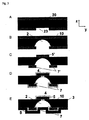
図4は本発明のマイクロ流体装置の一例を加工するために使用され得る加工工程の一例を、x−z平面で示している、すなわち:A)両辺を保護層(20)(例えば銅のような金属)で被覆した基材(3)(例えばポリイミド、ポリカーボネート又は液晶ポリマー)を用意すること;B)保護層(20)の両辺にフォトレジスト(21)を被覆すること;C)多重層の両辺に接するフォトレジスト層に二つの第一マスク(22及び22’)を構築(例えばフォトリソグラフによる)すること、これは基材にパターンをつけるマイクロ構造に対応する(本発明のいくつかの実施態様において、マスクは基材と直接は接触せずに、基材をエッチし望ましいマイクロ構造へ加工するためにレーザーフォトアブレーションが使用される場合のように離れている);D)基材の部分を露出するように多重層体層両辺に接する保護層に最終的なマスク(23、23’)を加工すること(例えば化学エッチングによる);E)単数又は複数のシールしていないマイクロ構造(2’)(ここではアクセスホール(9)を有する)を造るために、マスク(23及び23’)を介して基材に傷をつけること(好ましくはアンダーエッチングによりマスク(10)の下方の基材材料の部分を除去するために等方性のエッチングプロセスを使用する);F)マイクロシステムのオーム抵抗を減らすために役立つ最終導電手段(7)及び最終導電パッド(5)をそれぞれ造るのに役立つ導電パッド(5’及び7’)を造るために、基材を被覆している保護層の不必要な部分を除去すること(例えば化学エッチングによる);G)単数又は複数の電極(4)(これは相互接続されてもされていなくてもよく、そして参照電極、作用電極及び/又は対抗電極を造ってもよい)を造るために、導電パッド(5’)の上方に基材をさらに構築すること、そして、必要に応じて、被覆した電極(5)及び導電パッド(7)を造るために、導電パッド(例えば限定はしないが金のような不活性金属の電気メッキによって)を被覆すること;図4に示すように、この電極加工工程のために使用されるプロセス(たとえば、レーザーフォトアブレーション、エッチング、機械的除去、等)に応じて、この電極は異なる形状を有してもよく及び/又はマイクロ構造において異なる形状に曝されててもよく(突き出ている、平坦な又は埋め込まれた電極(基材に真っ直ぐ又は傾いた壁を伴う))さらに異なる幾何学形状(丸、多角形又はさらには画定していない形状)に曝されてもよい;G)最後に、多くの用途のために、被覆層(8)が最後にこの装置に加えられ(例えばポリマー層の糊付け又はラミネート加工による)、これによってマイクロ流体操作が可能となる。 FIG. 4 shows an example of processing steps that can be used to process an example of the microfluidic device of the present invention in the xz plane, ie: A) both sides of the protective layer (20) (eg, copper A base material (3) (for example, polyimide, polycarbonate, or liquid crystal polymer) coated with a metal); B) coating a photoresist (21) on both sides of the protective layer (20); Building two first masks (22 and 22 ') on the photoresist layer on both sides (eg by photolithography), which corresponds to a microstructure that patterns the substrate (some implementations of the invention). In embodiments, the mask is not in direct contact with the substrate, but is separated as when laser photoablation is used to etch and process the substrate into the desired microstructure. D) processing the final mask (23, 23 ') on the protective layer in contact with both sides of the multilayer body layer so as to expose portions of the substrate (eg by chemical etching); E) singular or Scratching (preferably under-etching) the substrate through masks (23 and 23 ') to create a plurality of unsealed microstructures (2'), here with access holes (9) Using an isotropic etching process to remove portions of the substrate material under the mask (10)); F) Final conductive means (7) and final conductive to help reduce the ohmic resistance of the microsystem Removing unnecessary portions of the protective layer covering the substrate (e.g. chemical etching) to make conductive pads (5 'and 7'), which are useful for making the pads (5) respectively. G) to make one or more electrodes (4) (which may or may not be interconnected and may make a reference electrode, a working electrode and / or a counter electrode) In order to further build a substrate above the conductive pad (5 ′) and, if necessary, to create a coated electrode (5) and conductive pad (7), a conductive pad (eg, but not limited to gold To the process used for this electrode processing step (eg, laser photoablation, etching, mechanical removal, etc.), as shown in FIG. Depending on the case, the electrodes may have different shapes and / or be exposed to different shapes in the microstructure (protruding, flat or embedded electrodes (straight or straight to the substrate or With inclined walls))) may be exposed to further different geometric shapes (round, polygonal or even undefined shapes); G) Finally, for many applications, the coating layer (8) Is finally added to the device (eg, by gluing or laminating polymer layers), which allows microfluidic manipulation.
図5は図4と同様の一組の加工工程を示すが、y−z平面のものでありそして図4D〜4Hの工程にのみ対応する。4D〜4Hは、すなわち、図5Aは図4Dをy−z平面から表したものであり、図5Bは図4Eに対応し、図5Eに対応する図4Hまで同様である。 FIG. 5 shows a set of processing steps similar to FIG. 4, but in the yz plane and corresponds only to the steps of FIGS. 4D to 4H, that is, FIG. 5A represents FIG. 4D from the yz plane, FIG. 5B corresponds to FIG. 4E, and so on up to FIG. 4H corresponding to FIG.
本発明の方法の有利で随意的な特徴の一つは金属マスクを使用してマイクロ構造を基材に造り、その後それ自体が導電手段としての役目を果たすようなやり方で構築されることに存する。等方性エッチングプロセスは基材をマイクロ構造化するために使用されてもよく、そしてこのような方法の一つの利点は導電手段がまずマイクロ構造の製造のためのマスクとしての役目を果たすという事実を当てにしており、これは、等方性エッチング工程の間に、結果として基材材料の除去をマスクの空いている部分だけでなくアンダーエッチ(10)のおかげでマスクの下方にももたらし、それによって被覆層でマイクロ構造をカバーした後でも大きな接触表面を提供し、これはマイクロ構造に存在する溶液が導電手段と物理的に接触することを可能にし、それによりマイクロ構造に沿ってオーム抵抗を減少させることが可能になる。 One advantageous and optional feature of the method of the present invention resides in the use of a metal mask to build the microstructure on the substrate, which is then constructed in such a way as to serve itself as a conductive means. . Isotropic etching processes may be used to microstructure the substrate, and one advantage of such a method is the fact that the conductive means first serves as a mask for the fabrication of the microstructure. Which, during the isotropic etching process, results in the removal of the substrate material not only in the empty part of the mask but also under the mask thanks to the underetch (10), Thereby providing a large contact surface even after covering the microstructure with a covering layer, which allows the solution present in the microstructure to be in physical contact with the conductive means, thereby providing an ohmic resistance along the microstructure. Can be reduced.
本実施態様は本発明の装置を加工するために使用される可能性のある手段を限定しない。例えばエンボス、射出成形、ポリマーキャスティング、ケイ素エッチング又はUV Liga(リソグラフィ電気メッキ成型)のような技術があるがこれらに限定はされず、これらの技術がマイクロ構造を加工するために使用され得る。 This embodiment does not limit the means that may be used to fabricate the apparatus of the present invention. Examples include, but are not limited to, techniques such as embossing, injection molding, polymer casting, silicon etching or UV Liga (lithographic electroplating), and these techniques can be used to process microstructures.
図6は本発明によるマイクロ流体装置の上面図を示し、マイクロ流体装置は作用電極(4)との接触を可能にする導電トラック(11及び11’)、外部世界(例えばポテンシオスタット、インピーダンス測定システム、マルチメーター及び/又はポテンシオスタット)へ接続するために役に立つパッド(12および12’)へそれぞれつながる擬似参照電極及び最終的には導電手段を伴う。図6の構成において、一体化した作用電極さらには参照電極(6)を支持し且つ画定するのに役立つ電気パッド(5)がマイクロ流体装置の上側辺に置かれ、一方で導電手段(7)及びそれに対応する伝導トラック(11’)及び(12’)はマイクロ構造基材の反対辺に置かれる。 FIG. 6 shows a top view of a microfluidic device according to the present invention, which is a conductive track (11 and 11 ′) allowing contact with the working electrode (4), the external world (eg potentiostat, impedance measurement). With pseudo reference electrodes and ultimately conductive means leading to pads (12 and 12 '), respectively, useful for connection to a system, multimeter and / or potentiostat. In the configuration of FIG. 6, an electrical pad (5) that serves to support and define the integrated working electrode as well as the reference electrode (6) is placed on the upper side of the microfluidic device, while conducting means (7). And corresponding conductive tracks (11 ′) and (12 ′) are placed on opposite sides of the microstructure substrate.
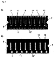
図7は75μm厚ポリイミドホイル(3)の写真(上側(A)及び下側(B)図)を表し、そこには図6に示されたものと同じ特徴を有する八つの独立したマイクロ流体装置がプラズマエッチングプロセスを使用して加工されている。 FIG. 7 represents a photograph (upper (A) and lower (B) views) of a 75 μm thick polyimide foil (3), in which eight independent microfluidic devices having the same characteristics as shown in FIG. Has been processed using a plasma etching process.
これらのマイクロ流体装置の各々は、1cm長さのマイクロチャンネル(2)、金で被覆した銅のサポート(5)(これは直径50μmでマイクロチャンネル壁に対して約15μm奥まったとことにある24つの作用電極を含む)、参照電極及び/又は対抗電極(Ag/AgClドットが使用されるがここでは示されない)のための金で被覆した銅パッド(6)、入口及び出口としての役目を果たすアクセスホール(9)、及びポテンシオスタットのような外部電気メーターに接続するために役立つ電気トラック(11)とパッド(12)を含む。ポリイミドサポート(3)の反対辺に、各装置はまた金で被覆した銅からできた導電手段(7)を含み、さらに例えば導電手段を対抗電極として接続するために使用されることができる接続をするために役立つパッド(12’)及び電気トラック(11’)を含む。本例において、導電手段はまずマイクロ構造をエッチするためのマスクとしての役目を果たすので、導電手段はマイクロチャンネル(2)を取り囲んでいる。導電手段を含む辺で、ポリイミドサポートは〜32μmまでの厚みのポリエチレン/ポリエチレンテレフタレート層で被覆されているが、図7ではその透明性のせいで見えない、そしてこれはシールしたマイクロチャンネル(2)を造ることを可能にする。 Each of these microfluidic devices has a 1 cm long microchannel (2), a gold-coated copper support (5) (which is 24 μm in diameter and about 15 μm deep with respect to the microchannel wall) A gold-coated copper pad (6) for the reference electrode and / or counter electrode (Ag / AgCl dots used but not shown here), access serving as inlet and outlet Includes holes (9) and electrical tracks (11) and pads (12) that serve to connect to an external electrical meter such as a potentiostat. On the opposite side of the polyimide support (3), each device also includes a conductive means (7) made of copper coated with gold, and a connection that can be used, for example, to connect the conductive means as a counter electrode. Includes a pad (12 ') and an electrical track (11') that are useful for In this example, the conductive means first serves as a mask for etching the microstructure, so that the conductive means surrounds the microchannel (2). On the side containing the conductive means, the polyimide support is coated with a polyethylene / polyethylene terephthalate layer up to ~ 32 μm thick but is not visible in FIG. 7 due to its transparency, and this is a sealed microchannel (2) Allows you to build.
図7に関連して短く上述したように、導電手段(7)は例えば基材にマイクロ構造を造るため使用される金属マスクの残留部分であってもよい。これらの場合において、このマスクは溝彫りパターンを示し、これはエッチング又はアブレーション媒体(例えば湿潤エッチングの場合は化学溶液、物理又は乾燥エッチングの場合はプラズマ、又はフォトアブレーションの場合はレーザービーム)に基材を曝すことを可能にする。マイクロ構造はこのようにして、望ましいマイクロ構造(形状及び寸法)を形成するために必要な期間に基材をエッチング又はアブレーション媒体に曝すことによって、加工される。アクセスホール(概して入口及び/又は出口)が同様に(且つエッチングプロセスにおいてマイクロ構造に対して同時であってもよい)基材の反対辺に追加的なマスクを提供することによって加工可能であり、これは望ましい基材部分、例えば加工すべきマイクロ構造の脚に相当する部分、を曝露することが可能である。このやり方で、基材は両辺からエッチされ、そしてスルーホールが追加したマスクによって画定した場所に造られることを確実になるように曝露時間が選択される。この基材の両辺からエッチされる部分が正確に重なり合うように、このプロセスでは二つのマスクの間の正確な位置合わせが要求される。金属マスクの望ましくない部分が除去可能であり(一方電極のためのサポート、導電手段又はトラック若しくはパッドの接続としての役目を果たすことを要求される部分は維持する)、及びこの残留部分は電極(例えば金、銀、プラチナ、チタン又はそれらに類するもの)としての役目を果たすのに適している金属で被覆されてもよい。最終的に、マイクロ構造は基材の導電手段を有する側で閉じることが可能であり(例えば被覆層の糊付け又はラミネート加工によって)、この場合スルーホールも基材のこちら側で閉じられ、それにより基材の反対側からアクセスできる入口及び出口を伴うシールしたマイクロ構造が提供されるようなやり方で行われる。 As briefly described above in connection with FIG. 7, the conductive means (7) may be, for example, the remaining part of a metal mask used to create a microstructure on the substrate. In these cases, the mask exhibits a grooved pattern that is based on an etching or ablation medium (eg, a chemical solution for wet etching, a plasma for physical or dry etching, or a laser beam for photoablation). Allows to expose the material. The microstructure is thus processed by exposing the substrate to an etching or ablation medium for the period necessary to form the desired microstructure (shape and dimensions). Access holes (generally inlets and / or outlets) can be processed as well (and may be simultaneous to the microstructure in the etching process) by providing an additional mask on the opposite side of the substrate, This can expose the desired substrate portion, for example the portion corresponding to the legs of the microstructure to be processed. In this manner, the substrate is etched from both sides and the exposure time is selected to ensure that the through hole is built at the location defined by the added mask. This process requires precise alignment between the two masks so that the etched portions from both sides of the substrate overlap exactly. Undesirable portions of the metal mask can be removed (while maintaining the support for the electrodes, conductive means or portions required to serve as track or pad connections), and this remaining portion can be removed from the electrodes ( For example, it may be coated with a metal suitable to serve as gold, silver, platinum, titanium or the like. Eventually, the microstructure can be closed on the side of the substrate with the conductive means (eg by gluing or laminating the coating layer), in which case the through-hole is also closed on this side of the substrate, thereby This is done in such a way as to provide a sealed microstructure with an inlet and outlet accessible from the opposite side of the substrate.
マイクロ構造を閉じるために使用されるチップ基材の辺にある導電手段の存在はシーリングの役に立つ被覆層の適用を促進し得ることが着目される。図7で示されるマイクロ流体装置の加工の際に、比較的大規模の導電手段(7)はポリエチレン/ポリエチレンテレフタレートラミネート加工層を安定化させ、このラミネート加工層はマイクロ構造を遮断することがあるあらゆる結合又は変形を示すことは実際にはないことが経験的に実際に示される。 It is noted that the presence of conductive means on the side of the chip substrate used to close the microstructure can facilitate the application of a coating layer useful for sealing. During processing of the microfluidic device shown in FIG. 7, the relatively large conductive means (7) stabilizes the polyethylene / polyethylene terephthalate laminate layer, which may interrupt the microstructure. It has actually been shown empirically that it does not actually show any coupling or deformation.
図8は実際に材料を組み立て及び一体化した作用電極及び導電手段を説明し、一例としてラミネート加工層のようなものでマイクロ構造をシールする前の本発明の電気化学マイクロ流体センサーのものを説明する。この図8の写真は、図6で示されたものと同等の特性を有し且つ図4及び5と関連して述べられるものと同様のエッチングプロセスを使用する50μm厚のポリイミドホイルで製造されている、本発明の装置の断面を示す。この例において、構造物(2)(ここではマイクロチャンネル)の上部の周りにフリーズを形成している導電手段(7)は金(7”)で被覆した銅(7’)で出来ており、そして導電手段(7)の銅の部分(7’)は基材にマイクロ構造を造るために使用されたマスクの残留部分であり、一方銅の部分(7’)を被覆する金の層(7”)は露出した銅表面を電気メッキすることによって製造されている。この図はまた一体化した作用電極(4)のひとつも表し、マイクロ構造の入口及び出口(ここでは示されない)の加工のためのマスクとしての役目を果たす銅のサポート(5’)の境界の明瞭な部分を曝露できるように、この一体化した作用電極はマイクロ構造の底部にあるポリイミド基材の部分を除去することによって加工される。凹み部がその後マイクロ構造の底部に形成され、そして作用電極(4)はその後銅のサポート(5’)の露出部分に金を電気メッキすることによって形成される。 FIG. 8 illustrates the working electrode and the conductive means in which the materials are actually assembled and integrated, as an example of the electrochemical microfluidic sensor of the present invention prior to sealing the microstructure with a laminated layer or the like. To do. The photograph of FIG. 8 is fabricated with a 50 μm thick polyimide foil that has characteristics similar to those shown in FIG. 6 and uses an etching process similar to that described in connection with FIGS. 4 and 5. Figure 2 shows a cross section of the device of the invention. In this example, the conductive means (7) forming a freeze around the top of the structure (2) (here microchannel) is made of copper (7 ') coated with gold (7 "), And the copper part (7 ') of the conductive means (7) is the remaining part of the mask used to make the microstructure on the substrate, while the gold layer (7 covering the copper part (7') ") Is manufactured by electroplating the exposed copper surface. This figure also represents one of the integrated working electrodes (4), the boundary of the copper support (5 ') acting as a mask for the processing of the microstructure inlet and outlet (not shown here) This integrated working electrode is processed by removing the portion of the polyimide substrate at the bottom of the microstructure so that a clear portion can be exposed. A recess is then formed in the bottom of the microstructure and the working electrode (4) is then formed by electroplating gold on the exposed portion of the copper support (5 ').
本発明の対象はポリマーマイクロ流体装置(1)の加工によって説明され、ここで導電手段(7)はマイクロ構造(2)を取り囲む金被覆した銅の層であり、この特定の場合において、このマイクロ構造は両辺を銅で被覆したポリイミドホイルを等位性エッチングによって製造した1cmの長さ及び約100μmの直径のマイクロチャンネルである。作用電極(4)及び擬似参照電極(6)は金で被覆した銅の電極であり、これはそれぞれのパッド(12)によってポテンシオスタットへ接続される。作用電極配列(4)は直径50μmのマイクロ電極24つで構成される。本マイクロ構造はポリエチレン及びポリエチレンテレフタレートでできた32μm厚さの層のラミネート加工によってシールされる。導電手段(7)がない場合の0.5mMフェロセンカルボン酸の検知を図9に表した、ここではサイクリックボルタメトリーを使用してより大きな電流が発生したときの抵抗の影響を明らかにする。実際に、電流の強度はボルタメトリーのスキャン速度とともに上昇する。低スキャン速度では、ボルタモグラムはピークからピークまで約100mV離れている前進波と後退波を良好に示し、ここでより高いスキャン速度では、このピークは前進スキャンではより大きなポテンシャル値へ移動し、後退スキャンではより小さなポテンシャル値へ移動する。この過剰なポテンシャルはマイクロチャンネルに沿った約1MΩの抵抗によるものであり、これは0.4μAを超える場合、iR降下は約0.4Vであることを意味する。これは実際には変形信号として測定されるものである。導電手段(7)がチップに加えられそしてパッド(12)によって対抗電極としてポテンシオスタットには接続されていないときに、図10(ここではボルタモグラム変形することなく1μAまでの電流がマイクロ構造(2)を通過する)で示されるように、このiR降下はほとんど零である。 The subject of the present invention is illustrated by the processing of the polymer microfluidic device (1), where the conductive means (7) is a gold-coated copper layer surrounding the microstructure (2), in this particular case this micro The structure is a microchannel with a length of 1 cm and a diameter of about 100 μm, produced by isotropic etching of a polyimide foil coated on both sides with copper. The working electrode (4) and the pseudo reference electrode (6) are copper electrodes coated with gold, which are connected to the potentiostat by respective pads (12). The working electrode array (4) is composed of 24 microelectrodes having a diameter of 50 μm. The microstructure is sealed by laminating a 32 μm thick layer of polyethylene and polyethylene terephthalate. Detection of 0.5 mM ferrocenecarboxylic acid in the absence of conducting means (7) is represented in FIG. 9, where the effect of resistance when larger currents are generated using cyclic voltammetry. In fact, the current intensity increases with the voltammetric scan rate. At low scan speeds, the voltammogram shows good forward and backward waves that are about 100 mV away from peak to peak, where at higher scan speeds, this peak moves to a larger potential value in forward scans, and backward scans Then move to a smaller potential value. This excess potential is due to a resistance of about 1 MΩ along the microchannel, which means that if it exceeds 0.4 μA, the iR drop is about 0.4V. This is actually measured as a deformation signal. When conducting means (7) is applied to the chip and not connected to the potentiostat as a counter electrode by the pad (12), current up to 1 μA without deformation of the voltammogram in FIG. This iR drop is almost zero, as shown by
本発明の一つの実施態様において、生じる逆反応に応じて、導電手段(7)は対抗電極として接続されてもよいし、されなくてもよい。例えば、対抗電極が作用電極(4)を汚染することがある場合、マイクロ構造(2)の外側、マイクロ構造の入口及び/又は出口にある溶液と接触して置かれている擬似参照電極で、二電極モードで作動しているポテンシオスタットを伴って、この反応を生じさせることがより良いだろう。このシステムはまだ十分に稼働しており、そして導電手段(7)は、接続されていなくても、なお大きなiR降下を回避している。可逆の又は擬似可逆の反応が存在するところでは、対抗電極としての導電手段(7)の接続が図11で示されるような作用電極(4)で検知された少なくともいくつかの分子を再生させることを可能にする。導電手段(7)が接続されていないとき(これは二電極モードにおける検知システムに相当する)、作用電極配列(4)に適用される電圧はフェロセンカルボン酸の酸化を可能にし、結果として測定されるアンペロメトリック電流は継続的に降下する、なぜなら低減したフェロセン分子は直ぐにマイクロ構造(2)において減少し、且つそれゆえに作用電極周りの体積が減少し、これがアンペロメトリック測定の時間スケールで探査されるからである。別の例では、同じマイクロ流体装置(1)が三電極モードで接続され、対抗電極としての導電手段(7)及びマイクロ構造入口又は出口に置かれた参照電極を伴う場合(すなわち金で被覆した銅パッドに付着したAg/AgClインクドット)、作用電極で酸化された分子はその後対抗電極で還元され、結果としてリサイクルプロセスが確立され、これは酸化した分子をフェロセンカルボン酸へ戻す再生を可能にする。この再生プロセスは直ぐに平衡状態に達し、結果として定常状態の電流が測定される。 In one embodiment of the invention, the conducting means (7) may or may not be connected as a counter electrode, depending on the reverse reaction that occurs. For example, if the counter electrode may contaminate the working electrode (4), a pseudo reference electrode placed in contact with the solution outside the microstructure (2), at the microstructure inlet and / or outlet, It would be better to produce this reaction with a potentiostat operating in two-electrode mode. The system is still fully operational, and the conductive means (7) still avoids large iR drops even if not connected. Where there is a reversible or quasi-reversible reaction, the connection of the conductive means (7) as the counter electrode regenerates at least some molecules detected at the working electrode (4) as shown in FIG. Enable. When the conductive means (7) is not connected (this corresponds to a sensing system in two-electrode mode), the voltage applied to the working electrode array (4) allows the oxidation of ferrocenecarboxylic acid and is measured as a result. The amperometric current continuously drops because the reduced ferrocene molecule immediately decreases in the microstructure (2) and hence the volume around the working electrode decreases, which is explored on the time scale of the amperometric measurement Because it is done. In another example, the same microfluidic device (1) is connected in a three-electrode mode, with conductive means (7) as a counter electrode and a reference electrode placed at the microstructure entrance or exit (ie coated with gold) Ag / AgCl ink dots attached to the copper pad), molecules oxidized at the working electrode are then reduced at the counter electrode, resulting in the establishment of a recycling process, which allows regeneration of the oxidized molecules back to ferrocenecarboxylic acid To do. This regeneration process immediately reaches equilibrium, and as a result, steady state current is measured.
いくつかの場合において、例えばマイクロ構造で酵素反応が生じるとき、検出すべき検体の濃度は時間と共に増加し、結果としてその濃度はiR降下することなくチップを通過することが困難な電流強度を生じる濃度に到る。結果として、電位−電流応答が移動しそして所与の電位での電流はオーム(iR)降下のために横ばい状態に達する。この事例は、加水分解したp−アミノフェノールリン酸塩アルカリリン酸塩(ALP)を用いて200mVで検知をする際の図12に示される。マイクロ流体装置(1)が導電手段(7)を有しないとき、検知から数秒後に横ばい状態に達する。対照的に、本発明による導電手段(7)を有するマイクロ流体装置(1)を伴う場合、同じ反応がより線形的な形状を示す。この特徴は従って例えば電気化学検知を伴うバイオセンサー装置の最適化のために最も重要な関心事項である。 In some cases, for example when an enzymatic reaction occurs in the microstructure, the concentration of the analyte to be detected increases with time, resulting in a current intensity that is difficult to pass through the chip without iR dropping. The concentration is reached. As a result, the potential-current response shifts and the current at a given potential reaches a flat state due to an ohm (iR) drop. This case is shown in FIG. 12 when sensing at 200 mV using hydrolyzed p-aminophenol phosphate alkaline phosphate (ALP). When the microfluidic device (1) has no conducting means (7), it will level off after a few seconds after detection. In contrast, the same reaction shows a more linear shape with a microfluidic device (1) with conducting means (7) according to the invention. This feature is therefore the most important concern, for example for the optimization of biosensor devices with electrochemical sensing.
さらなる実施態様において、この酵素反応は導電手段(7)を有するマイクロ流体装置で検知可能であり、この場合対抗電極が接続されていてもされていなくてもよい。この場合、酵素加水分解の生成物(ここではアミノフェノール)はキノンイミドに酸化され得る。この酸化反応は可逆的であり、結果としてキノンイミドは対抗電極で又は検知すべき検体分子を再生するために作用電極の印加電位を反転することによってp−アミノフェノールに還元され得る。導電手段が対抗電極として接続されるこの場合には、キノンイミドの還元は対抗電極で行われ、そしてp−アミノフェノールの濃度はより大きくなり、従って反応中により大きな電流応答をもたらす。この事例は図12で示される。 In a further embodiment, this enzymatic reaction is detectable with a microfluidic device having a conducting means (7), in which case the counter electrode may or may not be connected. In this case, the product of enzymatic hydrolysis (here aminophenol) can be oxidized to quinoneimide. This oxidation reaction is reversible so that quinoneimide can be reduced to p-aminophenol at the counter electrode or by reversing the applied potential of the working electrode to regenerate the analyte molecule to be detected. In this case, where the conducting means is connected as a counter electrode, the reduction of the quinoneimide takes place at the counter electrode and the concentration of p-aminophenol is greater, thus leading to a greater current response during the reaction. This case is shown in FIG.
本発明の装置を適用する別の例として、図13は甲状腺ホルモン(TSH)のアンペロメトリック検知の際に得た電流の時間変化を示し、甲状腺ホルモン(TSH)の検知は血漿中の免疫吸着法(Elisa)と関連する酵素によって行われ、装置は(A)一体化した導電手段を伴わない(B)一体化した導電手段を伴うマイクロ流体センサー装置であり、両マイクロ流体装置は同等の幾何学的特性(すなわち〜1cmの長さ及び〜50μmの深さ)及びマイクロチャンネルの入口に置いたAg/AgCl電極を分別よく有するマイクロチャンネルを含み、図7で示されたものと同様であるが金を被覆した銅サポートで造られた一連の48つの金の作用電極を伴っている。今は、一体化した導電手段が対抗電極として接続され、そしてAg/AgCl電極は擬似参照電極として使用される。 As another example to which the apparatus of the present invention is applied, FIG. 13 shows a temporal change of current obtained during amperometric detection of thyroid hormone (TSH), and detection of thyroid hormone (TSH) is immunoadsorption in plasma. The device is performed by an enzyme associated with the method (Elisa) and the device is (A) a microfluidic sensor device with no integrated conducting means (B) with an integrated conducting means, both microfluidic devices having an equivalent geometry Similar to that shown in FIG. 7, including microchannels with differential characteristics (ie ˜1 cm length and ˜50 μm depth) and an Ag / AgCl electrode placed at the entrance of the microchannel. With a series of 48 gold working electrodes made of gold-coated copper support. Now an integrated conducting means is connected as a counter electrode and an Ag / AgCl electrode is used as a pseudo reference electrode.
血漿中のTSH濃度測定のために、マイクロ流体装置はまず坑TSHで被覆しそして仔牛の血清溶液を使用する非特異性の吸着に対して遮断(block)される。既知の濃度である56.1μUI/mLを有するTSH試料の培養の後、アルカリリン酸塩(ALP)で共役させ標識化した坑−TSHの溶液でマイクロチャンネルを満たした。それからアンペロメトリック測定により検知を、酵素基材としてp−アミノフェニルリン酸塩(PAPP)を伴いつつ、Ag/AgClに対して200mVの適用している種々の時間に、行った。この分析は両タイプのマイクロチップを伴って二度繰り返され、そして測定した電流の時間変化が図13に示す。チップが導電手段を全く有さないとき(曲線B)、電流は横ばい状態に達し、これは酵素反応の生成物の減少とマイクロチャンネルに沿った抵抗(iR降下)の組合せが信号の増加を制限することを意味する。チップが対抗電極として働く一体化した導電手段を伴う場合(曲線A)、測定した電荷は制限されずそして時間と共に継続的に上昇し、これはほとんどiR降下がないこと及び酸化した生成物の部分(即ちこの場合はキノンイミド)はp−アミノフェノールに還元されていることを示す。 For measuring TSH concentrations in plasma, the microfluidic device is first coated with anti-TSH and blocked against non-specific adsorption using calf serum solution. After incubation of a TSH sample with a known concentration of 56.1 μUI / mL, the microchannels were filled with a solution of anti-TSH conjugated and labeled with alkaline phosphate (ALP). Detection was then performed by amperometric measurements at various times with 200 mV applied to Ag / AgCl with p-aminophenyl phosphate (PAPP) as the enzyme substrate. This analysis was repeated twice with both types of microchips, and the measured current over time is shown in FIG. When the chip has no conducting means (curve B), the current reaches a level, which is a combination of reduced enzyme reaction product and resistance along the microchannel (iR drop) limiting the signal increase. It means to do. When the chip is accompanied by an integrated conducting means that acts as a counter electrode (curve A), the measured charge is not limited and rises continuously with time, which means that there is little iR drop and part of the oxidized product (That is, quinonimide in this case) is reduced to p-aminophenol.
ここで電極のサイズが図13Aと13Bで示されたデータを出すために使用した装置で正確には同じではないことを強調しておく。マイクロチャンネルの長手方向部に沿った導電手段を含む装置は導電性手段を有さない装置より小さい作用電極を有する(直径が約50μmではなく約30μm)。これがなぜ測定の最初の部分で測定した電流が図13Bより図13Aで若干低いのかを説明する。両システムが完全に同一の幾何学的特性及び寸法(電極サイズも含む)を有する場合、測定の最初の部分において電流応答はほぼ同等になるはずである。検体の濃度がこれらの試験時間と共に増加するにつれて、図13Bでは導電手段がないために測定電流は数分後に飽和し、これはiR降下の増大を生じさせそして高濃度で測定可能な電流を制限する電位の移動を生じさせる。このようなアンペロメトリック測定において、印加される電位は実際にはポテンシオスタットにおける所与の値に固定され、結果として作用電極と擬似参照電極との間に効果的に印加される電圧が実際にiR降下の値により減少される。従来の電気化学システムにおいては、電位の減少は過剰電位の印加により補償されるべきであった、これはセンサーでは実施が困難である(あきらかに、印加すべき電位の追加は溶液の性質、装置の幾何学的形状、及び本例のように時間と共に変化し得る検体の濃度によって決まるからである)。導電手段の一体化はiR降下を最小にすることを可能にし、そしてそれゆえ大電流を伴って印加される可能性のある電位の移動を補償するための器具を必要としない。これは実際に図13Aで確認され、これは明らかに測定した電流が常に増加していることを示し、これはマイクロシステムの全体の抵抗が最小にされているからであり、結果としてiR降下は常に小さく、大電流を伴う場合でも小さい。 It is emphasized here that the size of the electrodes is not exactly the same in the apparatus used to produce the data shown in FIGS. 13A and 13B. Devices that include conductive means along the length of the microchannel have a working electrode that is smaller than devices that do not have conductive means (diameter is about 30 μm instead of about 50 μm). This explains why the current measured in the first part of the measurement is slightly lower in FIG. 13A than in FIG. 13B. If both systems have exactly the same geometric properties and dimensions (including electrode size), the current response should be approximately equivalent in the first part of the measurement. As the analyte concentration increases with these test times, the measured current saturates after a few minutes due to the lack of conducting means in FIG. 13B, which causes an increase in iR drop and limits the measurable current at high concentrations. Cause a potential shift. In such amperometric measurements, the applied potential is actually fixed at a given value in the potentiostat, and as a result, the voltage effectively applied between the working electrode and the pseudo reference electrode is actually Is reduced by the value of the iR drop. In conventional electrochemical systems, the potential decrease should be compensated by the application of excess potential, which is difficult to implement with a sensor (apparently, the addition of potential to be applied depends on the nature of the solution, the device And the concentration of the analyte that can change with time as in this example). The integration of the conductive means makes it possible to minimize the iR drop and therefore does not require an instrument to compensate for potential movement that may be applied with high currents. This is actually confirmed in FIG. 13A, which clearly shows that the measured current is constantly increasing, because the overall resistance of the microsystem is minimized, and as a result, the iR drop is Always small and small even with large currents.
さらなる実施態様において、完全な組立品を固めて且つ安定化するために、本発明のマイクロ流体装置は上部層(10)を含み、好ましくはポリマーから構成される。この上部層(30)は図14及び15で説明され、これは対応するカートリッジの図面を示し、そしてこの上部層は異なる構成要素を含んでもよく、異なる機能を果たしてもよい、例えば:
a)本事例においてホール(31)でできた入射口(又は入口)貯留槽であって、効果的に貯留槽を空にできるように、マイクロチャンネルの入射口が貯留槽の壁の底部にあるようなやり方で、ホールが置かれる、
b)他の貯留槽(32)は乾燥した又は湿潤の試薬又は溶液の貯蔵を可能にする、
c)マイクロ流体装置を操作し、そしてそれを簡単に器具のインターフェース(例えば流体及び/又は電気接続用)に接触させて置くためのポジションガイド(33);これらのポジションガイドはなおマイクロ流体装置(12’)の上部(トップ)及び下部(バック)サイドに伝導トラック(12)接続のための空間をのこしている。
In a further embodiment, to solidify and stabilize the complete assembly, the microfluidic device of the present invention comprises a top layer (10), preferably composed of a polymer. This top layer (30) is illustrated in FIGS. 14 and 15, which show the corresponding cartridge drawings, and this top layer may contain different components and may serve different functions, for example:
a) In this case, the entrance (or entrance) reservoir formed by the hole (31), and the entrance of the microchannel is at the bottom of the reservoir wall so that the reservoir can be effectively emptied The hall is placed in such a way,
b) Another reservoir (32) allows storage of dry or wet reagents or solutions,
c) Position guides (33) for manipulating the microfluidic device and placing it in contact with the instrument interface (eg for fluid and / or electrical connection) simply; these position guides are still microfluidic devices ( 12 ′) has a space for connecting the conductive track (12) on the upper (top) and lower (back) sides.
本発明のマイクロ流体装置は分析用途において都合よく利用可能であり、例えば限定はしないが電気化学センサ、イオンスプレーのイオン化によるサンプリング又は毛管電気泳動での検知器がある。 The microfluidic device of the present invention can be conveniently used in analytical applications such as, but not limited to, electrochemical sensors, sampling by ion spray ionization, or detectors in capillary electrophoresis.
本発明の特定の実施態様が添付図面を参照しながら説明される(しかしここで示される特徴に限定されることはない)。 Particular embodiments of the present invention will be described with reference to the accompanying drawings (but not limited to the features shown here).
Claims (49)
Applications Claiming Priority (2)
| Application Number | Priority Date | Filing Date | Title |
|---|---|---|---|
| US62705504P | 2004-11-12 | 2004-11-12 | |
| PCT/EP2005/012112 WO2006050972A1 (en) | 2004-11-12 | 2005-11-11 | Microfluidic device with minimised ohmic resistance |
Publications (2)
| Publication Number | Publication Date |
|---|---|
| JP2008519969A true JP2008519969A (en) | 2008-06-12 |
| JP2008519969A5 JP2008519969A5 (en) | 2008-12-25 |
Family
ID=35503966
Family Applications (1)
| Application Number | Title | Priority Date | Filing Date |
|---|---|---|---|
| JP2007540593A Pending JP2008519969A (en) | 2004-11-12 | 2005-11-11 | Microfluidic device with minimization of ohmic resistance |
Country Status (5)
| Country | Link |
|---|---|
| US (1) | US20070240986A1 (en) |
| EP (1) | EP1817576A1 (en) |
| JP (1) | JP2008519969A (en) |
| CN (1) | CN101057136A (en) |
| WO (1) | WO2006050972A1 (en) |
Families Citing this family (74)
| Publication number | Priority date | Publication date | Assignee | Title |
|---|---|---|---|---|
| US6391005B1 (en) | 1998-03-30 | 2002-05-21 | Agilent Technologies, Inc. | Apparatus and method for penetration with shaft having a sensor for sensing penetration depth |
| US8641644B2 (en) | 2000-11-21 | 2014-02-04 | Sanofi-Aventis Deutschland Gmbh | Blood testing apparatus having a rotatable cartridge with multiple lancing elements and testing means |
| US7344507B2 (en) | 2002-04-19 | 2008-03-18 | Pelikan Technologies, Inc. | Method and apparatus for lancet actuation |
| US9226699B2 (en) | 2002-04-19 | 2016-01-05 | Sanofi-Aventis Deutschland Gmbh | Body fluid sampling module with a continuous compression tissue interface surface |
| US7981056B2 (en) | 2002-04-19 | 2011-07-19 | Pelikan Technologies, Inc. | Methods and apparatus for lancet actuation |
| US9427532B2 (en) | 2001-06-12 | 2016-08-30 | Sanofi-Aventis Deutschland Gmbh | Tissue penetration device |
| WO2002100254A2 (en) | 2001-06-12 | 2002-12-19 | Pelikan Technologies, Inc. | Method and apparatus for lancet launching device integrated onto a blood-sampling cartridge |
| US8337419B2 (en) | 2002-04-19 | 2012-12-25 | Sanofi-Aventis Deutschland Gmbh | Tissue penetration device |
| US9795747B2 (en) | 2010-06-02 | 2017-10-24 | Sanofi-Aventis Deutschland Gmbh | Methods and apparatus for lancet actuation |
| US7041068B2 (en) | 2001-06-12 | 2006-05-09 | Pelikan Technologies, Inc. | Sampling module device and method |
| ES2336081T3 (en) | 2001-06-12 | 2010-04-08 | Pelikan Technologies Inc. | SELF-OPTIMIZATION PUNCTURE DEVICE WITH MEANS OF ADAPTATION TO TEMPORARY VARIATIONS IN CUTANEOUS PROPERTIES. |
| ATE485766T1 (en) | 2001-06-12 | 2010-11-15 | Pelikan Technologies Inc | ELECTRICAL ACTUATING ELEMENT FOR A LANCET |
| US9795334B2 (en) | 2002-04-19 | 2017-10-24 | Sanofi-Aventis Deutschland Gmbh | Method and apparatus for penetrating tissue |
| US8360992B2 (en) | 2002-04-19 | 2013-01-29 | Sanofi-Aventis Deutschland Gmbh | Method and apparatus for penetrating tissue |
| US8784335B2 (en) | 2002-04-19 | 2014-07-22 | Sanofi-Aventis Deutschland Gmbh | Body fluid sampling device with a capacitive sensor |
| US7909778B2 (en) | 2002-04-19 | 2011-03-22 | Pelikan Technologies, Inc. | Method and apparatus for penetrating tissue |
| US8221334B2 (en) | 2002-04-19 | 2012-07-17 | Sanofi-Aventis Deutschland Gmbh | Method and apparatus for penetrating tissue |
| US7491178B2 (en) | 2002-04-19 | 2009-02-17 | Pelikan Technologies, Inc. | Method and apparatus for penetrating tissue |
| US7674232B2 (en) | 2002-04-19 | 2010-03-09 | Pelikan Technologies, Inc. | Method and apparatus for penetrating tissue |
| US8372016B2 (en) | 2002-04-19 | 2013-02-12 | Sanofi-Aventis Deutschland Gmbh | Method and apparatus for body fluid sampling and analyte sensing |
| US7901362B2 (en) | 2002-04-19 | 2011-03-08 | Pelikan Technologies, Inc. | Method and apparatus for penetrating tissue |
| US7229458B2 (en) | 2002-04-19 | 2007-06-12 | Pelikan Technologies, Inc. | Method and apparatus for penetrating tissue |
| US7892183B2 (en) | 2002-04-19 | 2011-02-22 | Pelikan Technologies, Inc. | Method and apparatus for body fluid sampling and analyte sensing |
| US7547287B2 (en) | 2002-04-19 | 2009-06-16 | Pelikan Technologies, Inc. | Method and apparatus for penetrating tissue |
| US7297122B2 (en) | 2002-04-19 | 2007-11-20 | Pelikan Technologies, Inc. | Method and apparatus for penetrating tissue |
| US8702624B2 (en) | 2006-09-29 | 2014-04-22 | Sanofi-Aventis Deutschland Gmbh | Analyte measurement device with a single shot actuator |
| US9248267B2 (en) | 2002-04-19 | 2016-02-02 | Sanofi-Aventis Deustchland Gmbh | Tissue penetration device |
| US7198606B2 (en) | 2002-04-19 | 2007-04-03 | Pelikan Technologies, Inc. | Method and apparatus for a multi-use body fluid sampling device with analyte sensing |
| US8579831B2 (en) | 2002-04-19 | 2013-11-12 | Sanofi-Aventis Deutschland Gmbh | Method and apparatus for penetrating tissue |
| US7976476B2 (en) | 2002-04-19 | 2011-07-12 | Pelikan Technologies, Inc. | Device and method for variable speed lancet |
| US8267870B2 (en) | 2002-04-19 | 2012-09-18 | Sanofi-Aventis Deutschland Gmbh | Method and apparatus for body fluid sampling with hybrid actuation |
| US7232451B2 (en) | 2002-04-19 | 2007-06-19 | Pelikan Technologies, Inc. | Method and apparatus for penetrating tissue |
| US7331931B2 (en) | 2002-04-19 | 2008-02-19 | Pelikan Technologies, Inc. | Method and apparatus for penetrating tissue |
| US9314194B2 (en) | 2002-04-19 | 2016-04-19 | Sanofi-Aventis Deutschland Gmbh | Tissue penetration device |
| US8574895B2 (en) | 2002-12-30 | 2013-11-05 | Sanofi-Aventis Deutschland Gmbh | Method and apparatus using optical techniques to measure analyte levels |
| EP1628567B1 (en) | 2003-05-30 | 2010-08-04 | Pelikan Technologies Inc. | Method and apparatus for fluid injection |
| EP1633235B1 (en) | 2003-06-06 | 2014-05-21 | Sanofi-Aventis Deutschland GmbH | Apparatus for body fluid sampling and analyte sensing |
| WO2006001797A1 (en) | 2004-06-14 | 2006-01-05 | Pelikan Technologies, Inc. | Low pain penetrating |
| US8282576B2 (en) | 2003-09-29 | 2012-10-09 | Sanofi-Aventis Deutschland Gmbh | Method and apparatus for an improved sample capture device |
| WO2005037095A1 (en) | 2003-10-14 | 2005-04-28 | Pelikan Technologies, Inc. | Method and apparatus for a variable user interface |
| WO2005065414A2 (en) | 2003-12-31 | 2005-07-21 | Pelikan Technologies, Inc. | Method and apparatus for improving fluidic flow and sample capture |
| US7822454B1 (en) | 2005-01-03 | 2010-10-26 | Pelikan Technologies, Inc. | Fluid sampling device with improved analyte detecting member configuration |
| EP1751546A2 (en) | 2004-05-20 | 2007-02-14 | Albatros Technologies GmbH & Co. KG | Printable hydrogel for biosensors |
| WO2005120365A1 (en) | 2004-06-03 | 2005-12-22 | Pelikan Technologies, Inc. | Method and apparatus for a fluid sampling device |
| US9775553B2 (en) | 2004-06-03 | 2017-10-03 | Sanofi-Aventis Deutschland Gmbh | Method and apparatus for a fluid sampling device |
| US8652831B2 (en) | 2004-12-30 | 2014-02-18 | Sanofi-Aventis Deutschland Gmbh | Method and apparatus for analyte measurement test time |
| GB0607205D0 (en) * | 2006-04-10 | 2006-05-17 | Diagnoswiss Sa | Miniaturised biosensor with optimized anperimetric detection |
| EP2092321A1 (en) * | 2006-12-12 | 2009-08-26 | Koninklijke Philips Electronics N.V. | Electrochemical sensor device, method of manufacturing the same |
| FR2922023A1 (en) * | 2007-10-05 | 2009-04-10 | Univ Paris 7 Denis Diderot | Electrochemical detection installation for detecting presence of biological compound e.g. HIV antibody in sample e.g. blood, comprises detection cell having internal wall and two electrodes, and active part extending in confined space |
| US20090242429A1 (en) * | 2008-01-07 | 2009-10-01 | Ravil Sitdikov | Electrochemical Biosensor |
| US20090288960A1 (en) * | 2008-02-12 | 2009-11-26 | Robert Rubin | Rapid Detection of Anti-Chromatin Autoantibodies in Human Serum using a Portable Electrochemical Biosensor |
| US7956571B2 (en) | 2008-04-08 | 2011-06-07 | The Gillette Company | Method and apparatus for measuring electrochemical properties |
| EP2265324B1 (en) | 2008-04-11 | 2015-01-28 | Sanofi-Aventis Deutschland GmbH | Integrated analyte measurement system |
| WO2009140509A1 (en) * | 2008-05-14 | 2009-11-19 | The Board Of Trustees Of The University Of Illinois | Microcavity and microchannel plasma device arrays in a single, unitary sheet |
| US9375169B2 (en) | 2009-01-30 | 2016-06-28 | Sanofi-Aventis Deutschland Gmbh | Cam drive for managing disposable penetrating member actions with a single motor and motor and control system |
| US9222819B2 (en) * | 2009-02-20 | 2015-12-29 | University Of Southern California | Tracking and controlling fluid delivery from chamber |
| US8965476B2 (en) | 2010-04-16 | 2015-02-24 | Sanofi-Aventis Deutschland Gmbh | Tissue penetration device |
| US8940141B2 (en) | 2010-05-19 | 2015-01-27 | Lifescan Scotland Limited | Analytical test strip with an electrode having electrochemically active and inert areas of a predetermined size and distribution |
| WO2012011810A1 (en) | 2010-07-22 | 2012-01-26 | Stichting Voor De Technische Wetenschappen | Lab-on-a-chip device, for instance for use of the analysis of semen |
| CN101949946B (en) * | 2010-09-03 | 2012-11-07 | 东华大学 | Method for producing photoelectrochemical microfluidic detection chip of three-electrode system |
| CN102095770A (en) * | 2010-11-22 | 2011-06-15 | 复旦大学 | Electrochemical sensor chip based on digital microfluidic technology |
| WO2014001382A1 (en) * | 2012-06-29 | 2014-01-03 | Roche Diagnostics Gmbh | Sensor element for detecting an analyte in a body fluid |
| CN103226127B (en) * | 2013-03-27 | 2015-02-18 | 清华大学 | Multi-channel micro-fluidic chip and mass spectrum combined device |
| CN104132988A (en) * | 2014-07-28 | 2014-11-05 | 南京邮电大学 | Preparation method of flexible organic ion-sensitive field effect transistor |
| DE102014113482B4 (en) * | 2014-09-18 | 2019-01-03 | Bruker Daltonik Gmbh | Ionization chamber with tempered gas supply |
| CA2966007C (en) | 2014-10-28 | 2019-10-22 | The Governing Council Of The University Of Toronto | Electrochemical metabolic activity detecting device |
| CN104605837B (en) * | 2014-12-23 | 2016-08-24 | 电子科技大学 | A kind of monitoring of pulse system based on microfluid sensor |
| US9925319B2 (en) * | 2015-04-02 | 2018-03-27 | Purdue Research Foundation | Methods and apparatuses for impedance-based gas detection for microfluidic systems |
| KR102540664B1 (en) * | 2015-11-03 | 2023-06-08 | 삼성전자주식회사 | Bio sensor and sensing method thereof |
| EP3485266A1 (en) * | 2016-07-15 | 2019-05-22 | Unisense A/S | Electrochemical sensor with thin film guard electrode |
| CN106861781B (en) * | 2017-04-10 | 2023-04-11 | 黑龙江科技大学 | Micro-channel preparation method for reducing fluid resistance based on surface nano-bubbles |
| EP3700422B1 (en) * | 2017-10-24 | 2023-02-22 | Roche Diabetes Care GmbH | Electrochemical sensor and method for producing thereof |
| DE102018112258B4 (en) * | 2018-05-22 | 2023-01-05 | Leibniz-Institut Für Festkörper- Und Werkstoffforschung Dresden E.V. | ACOUSTOFLUIDIC COMPONENTS AND PROCESSES FOR THEIR MANUFACTURE |
| CN113740400B (en) * | 2021-08-18 | 2023-10-24 | 淮阴工学院 | Analysis and detection device of closed bipolar electrode array with symmetrical reference electrode |
Citations (3)
| Publication number | Priority date | Publication date | Assignee | Title |
|---|---|---|---|---|
| JPH11352093A (en) * | 1998-06-11 | 1999-12-24 | Matsushita Electric Ind Co Ltd | Biosensor |
| JP2000097899A (en) * | 1998-09-24 | 2000-04-07 | エヌ・ティ・ティ・アドバンステクノロジ株式会社 | Minute-quantity on-life biosensor and its manufacture |
| JP2004219325A (en) * | 2003-01-16 | 2004-08-05 | Ntt Advanced Technology Corp | Electrochemical online type biosensor and its manufacturing method |
Family Cites Families (11)
| Publication number | Priority date | Publication date | Assignee | Title |
|---|---|---|---|---|
| EP0752099A1 (en) * | 1994-02-09 | 1997-01-08 | Abbott Laboratories | Diagnostic flow cell device |
| US6338790B1 (en) * | 1998-10-08 | 2002-01-15 | Therasense, Inc. | Small volume in vitro analyte sensor with diffusible or non-leachable redox mediator |
| GB0010957D0 (en) * | 2000-05-05 | 2000-06-28 | Novartis Ag | Compound & method |
| GB0103516D0 (en) * | 2001-02-13 | 2001-03-28 | Cole Polytechnique Federale De | Apparatus for dispensing a sample |
| US7037417B2 (en) * | 2001-03-19 | 2006-05-02 | Ecole Polytechnique Federale De Lausanne | Mechanical control of fluids in micro-analytical devices |
| GB0111438D0 (en) * | 2001-05-10 | 2001-07-04 | Cole Polytechnique Federale De | Polymer bonding by means of plasma activation |
| GB0116384D0 (en) * | 2001-07-04 | 2001-08-29 | Diagnoswiss Sa | Microfluidic chemical assay apparatus and method |
| GB0121189D0 (en) * | 2001-08-31 | 2001-10-24 | Diagnoswiss Sa | Apparatus and method for separating an analyte |
| DE10234564B4 (en) * | 2002-07-25 | 2005-06-02 | Senslab-Gesellschaft Zur Entwicklung Und Herstellung Bioelektrochemischer Sensoren Mbh | biosensor |
| GB0226160D0 (en) * | 2002-11-08 | 2002-12-18 | Diagnoswiss Sa | Apparatus for dispensing a sample in electrospray mass spectrometers |
| GB0300820D0 (en) * | 2003-01-14 | 2003-02-12 | Diagnoswiss Sa | Membrane-microchannel strip |
-
2005
- 2005-11-11 US US11/718,774 patent/US20070240986A1/en not_active Abandoned
- 2005-11-11 WO PCT/EP2005/012112 patent/WO2006050972A1/en active Application Filing
- 2005-11-11 CN CN200580038765.3A patent/CN101057136A/en active Pending
- 2005-11-11 JP JP2007540593A patent/JP2008519969A/en active Pending
- 2005-11-11 EP EP05806366A patent/EP1817576A1/en not_active Withdrawn
Patent Citations (3)
| Publication number | Priority date | Publication date | Assignee | Title |
|---|---|---|---|---|
| JPH11352093A (en) * | 1998-06-11 | 1999-12-24 | Matsushita Electric Ind Co Ltd | Biosensor |
| JP2000097899A (en) * | 1998-09-24 | 2000-04-07 | エヌ・ティ・ティ・アドバンステクノロジ株式会社 | Minute-quantity on-life biosensor and its manufacture |
| JP2004219325A (en) * | 2003-01-16 | 2004-08-05 | Ntt Advanced Technology Corp | Electrochemical online type biosensor and its manufacturing method |
Also Published As
| Publication number | Publication date |
|---|---|
| US20070240986A1 (en) | 2007-10-18 |
| CN101057136A (en) | 2007-10-17 |
| WO2006050972A1 (en) | 2006-05-18 |
| EP1817576A1 (en) | 2007-08-15 |
Similar Documents
| Publication | Publication Date | Title |
|---|---|---|
| JP2008519969A (en) | Microfluidic device with minimization of ohmic resistance | |
| US20090178935A1 (en) | Miniaturised Biosensor with Optimized Amperometric Detection | |
| US8354012B2 (en) | Electrochemical cell | |
| US6548311B1 (en) | Device and method for detecting analytes | |
| Pumera et al. | New materials for electrochemical sensing VII. Microfluidic chip platforms | |
| US20060141469A1 (en) | Multi-layered electrochemical microfluidic sensor comprising reagent on porous layer | |
| Suzuki | Advances in the microfabrication of electrochemical sensors and systems | |
| Bratten et al. | Micromachining sensors for electrochemical measurement in subnanoliter volumes | |
| Gencoglu et al. | Electrochemical detection techniques in micro-and nanofluidic devices | |
| JP4216712B2 (en) | Microfluidic chemical assay device and method | |
| JP4777659B2 (en) | Integrated solid phase hydrophilic matrix circuit and microarray | |
| Suzuki et al. | An integrated three-electrode system with a micromachined liquid-junction Ag/AgCl reference electrode | |
| US20060207877A1 (en) | Microfluidic device with various surface properties fabricated in multilayer body by plasma etching | |
| US7988839B2 (en) | Capillary electrophoresis systems and methods | |
| KR20160097639A (en) | Biomolecular preconcentrator integrative electrical sensor and fabrication method thereof | |
| KR100563834B1 (en) | Micor/nano fluidic 3 dimensional electrode system | |
| CN111051885A (en) | Detection system and production method | |
| KR101924415B1 (en) | Multiple impedance measurement apparatus and method | |
| JP7362197B2 (en) | Biosensor with programmable sensing cavity | |
| Song et al. | Microfluidics for Chemical Analysis | |
| EP3812042A1 (en) | Ewod device with sensing apparatus | |
| CN117741117A (en) | Biosensing chip, biosensing chip manufacturing method and micro-channel system | |
| Li | Thomas J. Roussel 2, 4 Contact Information, Douglas J. Jackson 3 Contact Information, Richard P. Baldwin 4 Contact Information and Robert S. Keynton 2 Contact Information |
Legal Events
| Date | Code | Title | Description |
|---|---|---|---|
| A521 | Request for written amendment filed |
Free format text: JAPANESE INTERMEDIATE CODE: A523 Effective date: 20081110 |
|
| A621 | Written request for application examination |
Free format text: JAPANESE INTERMEDIATE CODE: A621 Effective date: 20081110 |
|
| A131 | Notification of reasons for refusal |
Free format text: JAPANESE INTERMEDIATE CODE: A131 Effective date: 20111206 |
|
| A02 | Decision of refusal |
Free format text: JAPANESE INTERMEDIATE CODE: A02 Effective date: 20120508 |