JP2007538331A - Integrated circuit and buffering method - Google Patents
Integrated circuit and buffering method Download PDFInfo
- Publication number
- JP2007538331A JP2007538331A JP2007517554A JP2007517554A JP2007538331A JP 2007538331 A JP2007538331 A JP 2007538331A JP 2007517554 A JP2007517554 A JP 2007517554A JP 2007517554 A JP2007517554 A JP 2007517554A JP 2007538331 A JP2007538331 A JP 2007538331A
- Authority
- JP
- Japan
- Prior art keywords
- data
- buffered
- processing module
- integrated circuit
- amount
- Prior art date
- Legal status (The legal status is an assumption and is not a legal conclusion. Google has not performed a legal analysis and makes no representation as to the accuracy of the status listed.)
- Pending
Links
Images

Classifications
-
- G—PHYSICS
- G06—COMPUTING; CALCULATING OR COUNTING
- G06F—ELECTRIC DIGITAL DATA PROCESSING
- G06F13/00—Interconnection of, or transfer of information or other signals between, memories, input/output devices or central processing units
- G06F13/38—Information transfer, e.g. on bus
- G06F13/42—Bus transfer protocol, e.g. handshake; Synchronisation
- G06F13/4204—Bus transfer protocol, e.g. handshake; Synchronisation on a parallel bus
- G06F13/4208—Bus transfer protocol, e.g. handshake; Synchronisation on a parallel bus being a system bus, e.g. VME bus, Futurebus, Multibus
Landscapes
- Engineering & Computer Science (AREA)
- Theoretical Computer Science (AREA)
- Physics & Mathematics (AREA)
- General Engineering & Computer Science (AREA)
- General Physics & Mathematics (AREA)
- Data Exchanges In Wide-Area Networks (AREA)
- Information Transfer Systems (AREA)
- Communication Control (AREA)
- Multi Processors (AREA)
Abstract
Description
本発明は、多数の処理モジュール及びこれら多数の処理モジュールを結合するインターコネクト(相互接続)手段を有している集積回路、バッファリング方法及びデータ処理システムに関する。 The present invention relates to an integrated circuit, a buffering method, and a data processing system having multiple processing modules and interconnect means for coupling the multiple processing modules.
システムオンシリコンは、新たな機構の実現と既存の機能を改善するための需要が増加の一途をたどっているために、複雑さが増し続けている。このことは、1つの集積回路上に集積化し得るコンポーネントの密度を高めることにより可能となる。同時に、回路を作動させるクロック速度も増加する傾向にある。コンポーネントの高密度化とあいまってクロック速度を高めるにつれて、同じクロックドメイン内で同期して作動させることのできる領域が縮小されている。これが、モジュラー手法の需要を創出した。このような手法によれば、処理システムは多数の、相対的に独立した複雑なモジュールを具える。従来の処理システムでは通常、システムのモジュールはバスを介して互いに通信する。しかしながら、このような通信方法は、モジュールの数が増加すると、もはや下記の理由により実用に供しなくなる。一方ではモジュールの数が多数になるとバスへの負荷が高くなり過ぎ、他方ではバスへデータを送信できるデバイスは1つだけであるため、バスが通信のボトルネックとなる。 System-on-silicon continues to increase in complexity as demand for new mechanisms and improvements to existing functions continues to increase. This is possible by increasing the density of components that can be integrated on a single integrated circuit. At the same time, the clock speed for operating the circuit also tends to increase. As the clock speed increases in conjunction with higher component density, the area that can be operated synchronously within the same clock domain is reduced. This created a demand for a modular approach. According to such an approach, the processing system comprises a number of relatively independent complex modules. In conventional processing systems, system modules typically communicate with each other via a bus. However, such a communication method is no longer practical for the following reasons when the number of modules increases. On the one hand, when the number of modules is large, the load on the bus becomes too high, and on the other hand, only one device can transmit data to the bus, so the bus becomes a communication bottleneck.
通信ネットワークは、これらの不都合を解消するのに有効な策を成している。ネットワークオンチップ(Networks on chip(NoC))は近年、非常に複雑なチップにおけるインターコネクトの問題に対する解決手法として、高い注目を集めている。この理由は2つから成る。第1に、NoCはグローバル配線を構築し管理するため、新しいディープサブミクロン技術における電気的課題を解決する助けとなる。NoCは配線を共有すると同時に、それらの個数を削減し利用性を高める。NoCは、電力効率及び信頼性をよくすることもでき、かつバスに比べて拡張性がある。第2にNoCは、莫大な数のトランジスタチップの設計を管理するのに必須である演算処理を通信から切り離す。NoCがこのような分離を実現できる理由は、これらのNoCはもともとは、プロトコルスタックを用いて設計されるからであり、プロトコルスタックは、通信サービスの利用をサービスの実装から分離するインターフェースを明確に規定する。 Communication networks are an effective way to eliminate these disadvantages. In recent years, Networks on chip (NoC) has attracted a great deal of attention as a solution to the interconnect problem in very complex chips. There are two reasons for this. First, NoC helps solve the electrical challenges in new deep submicron technology because it builds and manages global wiring. NoC shares wiring, and at the same time reduces their number and increases usability. NoC can improve power efficiency and reliability, and is more scalable than a bus. Secondly, the NoC decouples the computation processing that is essential to manage the design of a vast number of transistor chips. The reason why NoC can achieve such separation is because these NoCs are originally designed using protocol stacks, which clearly define the interface that separates the use of communication services from the implementation of services. Stipulate.
しかしながら、システムオンチップ(SoC)の設計時にオンチップ通信用のネットワークを用いると、考慮しなくてはならない多くの新しい問題を引き起こすことになる。これは、通信モジュールを直接接続する、既存のオンチップインターコネクト(例えば、バス、スイッチ、または二地点間配線など)とは対照的に、NoCでは、モジュールがネットワークノードを介して間接的に通信を行うからである。結果として、インターコネクトのアービトレーションが集中型から分散型に変わり、不調なトランザクション、高い待ち時間、及びエンド・ツー・エンドフロー制御といった問題を、インテレクチャル・プロパティ・ブロック(IP)か、またはネットワークによって処理しなければならなくなる。 However, using a network for on-chip communication when designing a system-on-chip (SoC) creates many new problems that must be considered. In contrast to existing on-chip interconnects that directly connect communication modules (for example, buses, switches, or point-to-point wiring), in NoC, modules communicate indirectly through network nodes. Because it does. As a result, interconnect arbitration has changed from centralized to decentralized, and problems such as bad transactions, high latency, and end-to-end flow control can be handled by intelligent property blocks (IP) or by the network. Will have to be processed.
これらの問題の大部分はすでに、ローカル及び広域ネットワーク(コンピュータ・ネットワーク)の分野における研究課題及び並列計算機のインターコネクトネットワーク用のインターコネクトとして存在していた。これらは共にネットワークオンチップに極めて関連しており、これらの分野での多くの実績は、チップにも適用することができる。しかしながら、NoCの前提はオフチップネットワークとは異なっているため、ネットワーク設計上の選択の大部分を再評価しなければならない。ネットワークオンチップは、設計上の選択を異にし、最終的にネットワークサービスに影響を及ぼす、種々の特性(例えば、強いリンク同期)や、制約(例えば、高いメモリコスト)を有する。 Most of these problems already existed as research issues in the field of local and wide area networks (computer networks) and as interconnects for parallel computer interconnect networks. Both of these are highly related to network-on-chip, and many achievements in these fields can also be applied to chips. However, since NoC's premise is different from off-chip networks, most of the network design choices must be re-evaluated. Network-on-chip has different characteristics (eg, strong link synchronization) and constraints (eg, high memory cost) that vary in design choice and ultimately affect network services.
オンチップインターコネクトとしてネットワークを導入することは、バスまたはスイッチのような直接的なインターコネクトと比較すると、通信を根本的に変化させることになる。これは、通信モジュールを直接接続せずに、1つまたは1つ以上のネットワークノードによって分離させるネットワークのマルチホップ性によるものである。このことは、モジュールを直接接続する、一般的な既存のインターコネクト(例えば、バス)とは対照的である。 Introducing a network as an on-chip interconnect will fundamentally change communication compared to a direct interconnect such as a bus or switch. This is due to the multi-hop nature of the network where communication modules are not directly connected but separated by one or more network nodes. This is in contrast to typical existing interconnects (eg, buses) that connect modules directly.
現代のオンチップ通信プロトコル(例えば、デバイス・トランザクション・レベルのDTL及びAXI-プロトコル)は、要求と応答から成るトランザクションで、スプリット及びパイプラインに基づいて動作し、バスは、マスタによって出された要求が対応するスレーブによって受け入れられた後に釈放されて、他に使用される。スプリット・パイプライン型の通信プロトコルは、特に、インターコネクトを効率的に利用できるようにするマルチホップ式のインターコネクト(例えば、ネットワークオンチップまたはブリッジを有するバス)において用いられる。スレーブにおける応答の生成に時間がかかる場合に、スプリットバスの効率を上げることができる。パイプラインプロトコルでは、マスタは複数の未処理の要求(すなわち、応答が保留中または期待されている要求)を有することができる。 Modern on-chip communication protocols (eg, device transaction level DTL and AXI-protocols) are request and response transactions that operate on a split and pipeline basis, where the bus is a request issued by the master. Released after being accepted by the corresponding slave and used elsewhere. Split-pipeline communication protocols are used in particular in multi-hop interconnects (eg, buses with network-on-chip or bridges) that allow the interconnect to be used efficiently. If it takes time to generate a response in the slave, the efficiency of the split bus can be increased. In a pipeline protocol, a master can have multiple outstanding requests (ie, requests for which a response is pending or expected).
上述したプロトコルは、システムまたはインターコネクトのレベルではなく、デバイスのレベルにて動作するように設計される。言い換えれば、前述のプロトコルは、インテレクチャル・プロパティ・ブロックIP及びそれらの初期のインテグレーションを再利用可能にする実際のインターコネクトの実現(例えば、アービトレーション信号は不可視である)とは無関係に設計される。 The protocols described above are designed to operate at the device level, not the system or interconnect level. In other words, the protocol described above is designed independently of the actual interconnect implementation that makes the intellectual property block IP and their initial integration reusable (eg, the arbitration signal is invisible). .
特に、前述のオンチップ通信プロトコルは、4つの主要な信号グループ、即ちコマンド(またはアドレス)、書込みデータ、読取りデータ、及び書込み応答を包含する。コマンドグループは、コマンド、アドレス、及びバースト長やマスクのようなコマンドフラグから成る。コマンド及び書込みデータグループは、ターゲットへのイニシエータによって駆動される。読取りデータと書込み応答は、イニシエータからのコマンドに追従して、このイニシエータへとターゲットによって駆動される。4つのグループは全て、何らかの順序をそれらの間に成して互いに独立しており、例えば、コマンドの前に応答が発せられることはない。 In particular, the aforementioned on-chip communication protocol includes four main signal groups: command (or address), write data, read data, and write response. The command group includes a command, an address, and a command flag such as a burst length and a mask. Command and write data groups are driven by the initiator to the target. Read data and write responses are driven by the target to this initiator following commands from the initiator. All four groups are independent of each other in some order, for example, no response is issued before the command.
これらのオンチップ通信プロトコルは、従来のチップ設計において周知の、データのバッファリングの概念も実現する。一般的にバッファリングは、1つのモジュールがデータを生成し、他のモジュールがデータを消費するように、異なるモジュールを分離するために用いられる。バッファリングを行わないと、消費モジュールが生成モジュールのデータを受け入れる準備が整うまで、生成モジュールは消費モジュールによって阻止されることになる。生成モジュールが阻止されないようにするためには、生成モジュールによって生成されたデータを格納するバッファを導入して、消費モジュールの準備が整っていなくても、生成モジュールがその実行を継続し得るようにする。消費モジュールが幾つか、または全てのバッファされたデータを受け入れる準備が整ったとき直ちに、バッファ内に格納されているデータが消費モジュールへと供給される。 These on-chip communication protocols also implement the concept of data buffering, well known in conventional chip design. In general, buffering is used to separate different modules so that one module generates data and the other module consumes data. Without buffering, the producing module will be blocked by the consuming module until the consuming module is ready to accept the producing module's data. In order to prevent the generation module from being blocked, a buffer for storing the data generated by the generation module is introduced so that the generation module can continue its execution even if the consumption module is not ready. To do. As soon as the consuming module is ready to accept some or all buffered data, the data stored in the buffer is supplied to the consuming module.
他方では、現代のオンチップ通信プロトコルは、インターコネクトの利用性を改善するために、書込みコマンドまたは書込みデータのバッファリングも用いている。したがって、小さい書込みバーストは、これらがインターコネクトを介して送信される前に、バッファ内に格納または蓄積される。蓄積されたデータは短いバーストで転送する代りに、インターコネクトを介して長いバーストで転送されることになり、これは通常インターコネクトの利用性の改善につながる。このことは、第1の書込みデータW1をバッファリングし、このデータを、例えば第2の書込みデータW2がバッファに到達するまでは転送しない(すなわち、第1の書込みデータはインターコネクトを介して転送されない)ようにし、書込みデータがインターコネクトの利用性に関して最適な長さを有する1つのバーストとして転送されるようにして実施することができる。 On the other hand, modern on-chip communication protocols also use write command or write data buffering to improve interconnect usability. Thus, small write bursts are stored or accumulated in a buffer before they are transmitted over the interconnect. Instead of transferring the accumulated data in short bursts, it will be transferred in long bursts over the interconnect, which usually leads to improved interconnect usability. This buffers the first write data W1 and does not transfer this data until, for example, the second write data W2 reaches the buffer (ie, the first write data is not transferred over the interconnect). And the write data is transferred as a single burst having the optimum length for interconnect availability.
したがって、多数の書込みからのデータをバッファして、1つのバーストに集約することができる。さらに、書込みコマンドにおけるデータの一部分は、別のバーストで送信することができる。 Thus, data from multiple writes can be buffered and aggregated into one burst. In addition, a portion of the data in the write command can be transmitted in another burst.
前述の、オンチップ通信プロトコルにて上述したようなバッファリング技法を実施する理由は、インターコネクトによって接続される、システムオンチップにおけるインテレクチャル・プロパティ・ブロックIPが、「固有に」通信できなくてはならない、すなわち、ワードの幅及びバーストサイズを、インターコネクトよりはむしろデバイスに適合するように構成しなくてはならないためである。例えば、インテレクチャル・プロパティ・ブロックIPがピクセルを処理する場合、これらのインテレクチャル・プロパティ・ブロックはピクセルを消費しかつ生成する一方で、それらがビデオフレームを処理している場合には、ビデオフレームを消費しかつ生成する。データをバッファリングすることによって、十分な量のデータを1つのバーストで一度に転送できるように集められるまで、インターコネクトを介して転送すべきデータを待機させる。 The reason for implementing the buffering technique as described above in the above-described on-chip communication protocol is that the intelligent property block IP in the system-on-chip connected by the interconnect cannot communicate “inherently”. This is because the word width and burst size must be configured to fit the device rather than the interconnect. For example, if the intelligent property block IP processes pixels, these intelligent property blocks consume and generate pixels while they are processing video frames, Consume and generate video frames. By buffering the data, it waits for data to be transferred over the interconnect until a sufficient amount of data has been collected so that it can be transferred in one burst.
上述したオンチッププロトコルは、主に、待ち時間の短いバス用に設計されている。さらに、これらのプロトコルは、読取り操作は常に緊急を要するために、不必要なバッファリングを行うことなくできるだけ早く完了させなければならない、という前提に基づいて設計されている。しかしながら、システムの大型化と、ネットワークまたはブリッジを有するバスのようなマルチホップ式のインターコネクトによって、待ち時間も同様に長くなっている。こういった場合には、通信精度が粗くなり、待ち時間の要求の正確さが低下する。 The on-chip protocol described above is designed primarily for buses with low latency. Furthermore, these protocols are designed on the assumption that read operations are always urgent and must be completed as soon as possible without unnecessary buffering. However, latency is similarly increased due to the increased size of the system and multi-hop interconnects such as buses with networks or bridges. In such a case, the communication accuracy becomes rough, and the accuracy of the waiting time request decreases.
さらにこれらのプロトコルは、無制限なデータのバッファリングが起因するデッドロックを回避するために最適なバースト長に到達していなくても、現在バッファされているデータの幾つかを転送させる手法を含んでいる。DTL通信プロトコルは、現在のワードまでの全てのデータを、インターコネクトで転送させるフラッシュ信号を提供している。AXIプロトコルは、バッファされたデータを転送させる書込みコマンド用のアンバッファフラグを提供している。 In addition, these protocols include techniques to transfer some of the currently buffered data even if the optimal burst length has not been reached to avoid deadlocks due to unlimited data buffering. Yes. The DTL communication protocol provides a flash signal that causes all data up to the current word to be transferred over the interconnect. The AXI protocol provides an unbuffer flag for a write command that causes buffered data to be transferred.
したがって、本発明の目的は、インターコネクトの利用性を改善した集積回路、バッファリング方法、並びにデータ処理システムを提供することにある。 Accordingly, it is an object of the present invention to provide an integrated circuit, a buffering method, and a data processing system with improved interconnect usability.
この目的は、請求項1に記載の集積回路、請求項13に記載のバッファリング方法、及び、請求項14に記載のデータ処理システムによって達成される。 This object is achieved by an integrated circuit according to claim 1, a buffering method according to claim 13, and a data processing system according to claim 14.
したがって、本発明によれば、インターコネクト手段によって結合される多数の処理モジュールを具える集積回路が提供される。第1の処理モジュールは、トランザクションに基づいて第2の処理モジュールと通信する。前記第2の処理モジュールに関連する第1のラッパー手段は、第1の量のデータがバッファされるまで、前記インターコネクト手段によって転送すべき前記第2の処理モジュールからのデータをバッファリングし、その後、前記第1の量のバッファされたデータを、前記第1の処理モジュールへと転送する。 Thus, according to the present invention, an integrated circuit is provided comprising a number of processing modules coupled by interconnect means. The first processing module communicates with the second processing module based on the transaction. The first wrapper means associated with the second processing module buffers data from the second processing module to be transferred by the interconnect means until a first amount of data is buffered, and thereafter , Transferring the first amount of buffered data to the first processing module.
したがってデータは、単一のパッケージでインターコネクトを介して転送すべきデータの量が十分に多量になるまで、スレーブ側にてバッファされる。インターコネクトを介して送信するパケットの数を低減すれば、必要なパケットヘッダが減るため、通信のオーバーヘッドが軽減される。送信すべきデータは、十分な量のデータが集められるまでバッファする。 Data is therefore buffered on the slave side until the amount of data to be transferred over the interconnect in a single package is large enough. If the number of packets to be transmitted through the interconnect is reduced, the required packet header is reduced, thereby reducing communication overhead. Data to be transmitted is buffered until a sufficient amount of data has been collected.
本発明の態様によれば、第2の量のデータがバッファされるまで、インターコネクト手段を介して前記第2の処理モジュールへ転送すべき前記第1の処理モジュールからのデータをバッファリングするために第2のラッパー手段を第1の処理モジュールに関連付けて、その後、前記第2のラッパー手段が、前記バッファされたデータを前記第2の処理モジュールへ転送し得るようにする。したがってデータは、インターコネクトを介して単一のパッケージで転送すべきデータの量が十分に多量になるまで、マスタ並びにスレーブ側にてバッファされる。 According to an aspect of the present invention, for buffering data from the first processing module to be transferred to the second processing module via the interconnect means until a second amount of data is buffered. Associating a second wrapper means with the first processing module so that the second wrapper means can then transfer the buffered data to the second processing module. Thus, data is buffered on the master and slave sides until the amount of data to be transferred in a single package over the interconnect is large enough.
本発明のさらなる態様によれば、前記第1及び第2のラッパー手段を、それぞれ、第1及び第2のアンバッファ信号または信号のグループの特定の組合せに応じて、(前記第1及び第2のラッパー手段にバッファされたデータが、前記第1及び第2の量より少なくても)バッファされたデータを転送するように適合させる。アンバッファ信号を発することにより、データがバッファされるのを待機する処理によるデッドロックの発生を阻止することができる。 According to a further aspect of the invention, the first and second wrapper means are respectively responsive to a particular combination of first and second unbuffered signals or groups of signals (the first and second Adapted to transfer the buffered data (even if the buffered data is less than the first and second quantities). By issuing the unbuffer signal, it is possible to prevent the occurrence of deadlock due to the process of waiting for the data to be buffered.
本発明のさらなる態様によれば、前記第1及び第2のラッパー手段を、それぞれ、第1及び第2のアンバッファフラグに従って、(前記第1及び第2のラッパー手段にバッファされたデータが、前記第1及び第2の量より少なくても)バッファされたデータを転送するように適合させる。したがって、バッファされたデータをフラッシュ(一括消去)するための代替方法が提供される。各トランザクションに対して与えられる信号とは対照的に、フラグは長めの時間に設定することができる。このようにして、バッファリングを実行させたり、停止させたりすることができる。フラグは、任意の方法、例えば、IPからの信号とともにトランザクションの一部として、または別のコンフィグレーションのトランザクション(特殊なフラッシュトランザクション、またはメモリーマップ式の読取りまたは書込み)を介して設定/解除することができる。これらのトランザクションは、同一のIPからか、または別のコンフィグレーションモジュールから出すことができる。 According to a further aspect of the invention, the first and second wrapper means are respectively in accordance with the first and second unbuffer flags (the data buffered in the first and second wrapper means is Adapt to transfer buffered data (even if less than said first and second amounts). Thus, an alternative method for flushing the buffered data is provided. In contrast to the signal provided for each transaction, the flag can be set to a longer time. In this way, buffering can be executed or stopped. Flags can be set / unset in any way, eg as part of a transaction with a signal from IP, or through another configuration transaction (special flash transaction, or memory-mapped read or write) Can do. These transactions can originate from the same IP or from different configuration modules.
本発明の好適な態様によれば、前記第1及び第2のラッパー手段の少なくとも1つが、前記第1と第2の処理モジュール間の前記通信の通信特性に従ってデータを転送する前に、前記第1または第2のラッパー手段にバッファすべきデータの最適な第1または第2の量を決定する決定ユニットBLDUを具えるようにする。したがって、インターコネクトを介して転送されるデータのパケットのサイズを、実際の通信の特性に応じて適合させることができるため、インターコネクトの利用性を改善することができる。 According to a preferred aspect of the present invention, at least one of the first and second wrapper means transfers the data before transferring data according to the communication characteristics of the communication between the first and second processing modules. A decision unit BLDU is provided for determining an optimum first or second amount of data to be buffered in the first or second wrapper means. Accordingly, the size of the packet of data transferred through the interconnect can be adapted according to the actual communication characteristics, so that the usability of the interconnect can be improved.
本発明は、インターコネクト手段に接続される多数の処理モジュールを有する集積回路内でデータをバッファリングする方法にも関し、第1の処理モジュールがトランザクションに基づいて第2の処理モジュールと通信する前記バッファリング方法が、第1の量のデータがバッファされるまで、インターコネクト手段を介して転送すべき前記第2の処理モジュールからのデータをバッファリングし、バッファされたデータは、前記第1の量のデータがバッファされたときに転送するステップを含むようにする。 The invention also relates to a method of buffering data in an integrated circuit having a number of processing modules connected to interconnect means, wherein the first processing module communicates with a second processing module based on a transaction. The ring method buffers data from the second processing module to be transferred via the interconnect means until the first amount of data is buffered, and the buffered data is stored in the first amount of data. It includes a step of transferring when data is buffered.
本発明はさらに、インターコネクト手段によって結合される多数の処理モジュールを具える集積回路を含む、データ処理システムにも関する。第1の処理モジュールは、トランザクションに基づいて、第2の処理モジュールと通信を行う。前記第1の処理モジュールに関連する第2のラッパー手段は、第1の量のデータがバッファされるまで、インターコネクト手段を介して転送すべき前記第1の処理モジュールからのデータをバッファリングし、その後、前記第1の量のバッファされたデータを、前記第1の処理モジュールへと転送する。 The invention further relates to a data processing system comprising an integrated circuit comprising a number of processing modules coupled by interconnect means. The first processing module communicates with the second processing module based on the transaction. Second wrapper means associated with the first processing module buffers data from the first processing module to be transferred through the interconnect means until a first amount of data is buffered; Thereafter, the first amount of buffered data is transferred to the first processing module.
したがって、上述のようなデータのバッファリングは、多数の集積回路を具えるシステムにも適用することができる。 Therefore, the buffering of data as described above can be applied to a system including a large number of integrated circuits.
本発明は、バッファされたデータがインターコネクトの手段を介してパケットで最適に転送されるように十分に大きくなるまでデータをバッファする、という考えに基づいて成したものである。パケットが大きくなるほど、パケットヘッダの量は少なくなり、オーバーヘッドが軽減され、インターコネクトがより効率よく利用される。データは、早く送信できても、最適なパケットサイズとなるのに十分なデータがバッファされたときにのみ転送される。データは、最適な転送の条件が満足されたときにのみ、バッファから転送される。 The present invention is based on the idea of buffering data until the buffered data is large enough to be optimally transferred in packets via the interconnect means. The larger the packet, the less packet header, the less overhead, and the more efficient use of the interconnect. Even if data can be transmitted quickly, it is transferred only when enough data is buffered to achieve the optimal packet size. Data is transferred from the buffer only when optimal transfer conditions are met.
本発明のさらなる態様は、従属項に記載した通りのものである。 Further aspects of the invention are as described in the dependent claims.
本発明のこれら及び他の態様は、これ以降に述べる実施例を参照して明らかにする。 These and other aspects of the invention will be apparent with reference to the examples described hereinafter.
以下の実施例は、システムオンチップに関し、すなわち、同一チップ上(例えば、パッケージ内のシステム、マルチダイ・モジュールなどを含む)または異なるチップ上の多数のモジュールが、ある種のインターコネクトを介して互いに通信するシステムオンチップに関する。インターコネクトは、ネットワークオンチップNoCとして具体化される。ネットワークオンチップは、配線、バス、時分割多重化、スイッチ、及び/またはルータをネットワーク内に具えることができる。前記ネットワークのトランスポート層では、モジュール間の通信はコネクションによって行うことができる。コネクションとは、各々が第1のモジュールと、少なくとも1つの第2のモジュールとの間に一組のコネクション特性を有している一組のチャネルとみなすことができる。第1のモジュールと単一の第2のモジュールとの間のコネクションに対して、そのコネクションは2つのチャネル、すなわち、第1のモジュールから第2のモジュールへの第1チャネル、すなわち要求チャネルと、第2のモジュールから第1のモジュールへの第2チャネル、すなわち応答チャネルとを具えることができる。要求チャネルは、第1モジュールから第2モジュールへのデータ及びメッセージ用に確保され、応答チャネルは第2モジュールから第1モジュールへのデータ及びメッセージ用に確保される。しかしながら、コネクションが1個の第1のモジュールとN個の第2のモジュールに関連する場合には、2×N個のチャネルを用意する。コネクションの特性には、順序付け(データ転送の順序)、フロー制御(遠隔バッファをコネクション用に確保して、データ生成モジュールは、生成したデータ用に利用できるスペースが保証された場合にのみデータを送信することができるようにする)、スループット(スループットの下限値を保証する)、待ち時間(待ち時間の上限値を保証する)、損失(データの脱落)、送信の終了、トランザクションの完了、データの正確さ、優先度、またはデータの配信を含めることができる。 The following examples relate to system-on-chip, i.e., multiple modules on the same chip (e.g., including systems in a package, including multi-die modules, etc.) or on different chips communicate with each other over some type of interconnect. It relates to system on chip. The interconnect is embodied as a network on chip NoC. The network on chip can include wiring, buses, time division multiplexing, switches, and / or routers in the network. In the transport layer of the network, communication between modules can be performed by connection. A connection can be viewed as a set of channels, each having a set of connection characteristics between a first module and at least one second module. For a connection between a first module and a single second module, the connection has two channels: a first channel from the first module to the second module, ie a request channel; There may be a second channel from the second module to the first module, ie a response channel. The request channel is reserved for data and messages from the first module to the second module, and the response channel is reserved for data and messages from the second module to the first module. However, if the connection is related to one first module and N second modules, 2 × N channels are prepared. Connection characteristics include ordering (data transfer order), flow control (remote buffer reserved for connection, data generation module sends data only when space available for generated data is guaranteed ), Throughput (guarante the lower limit of throughput), latency (guarante the upper limit of latency), loss (lost data), end of transmission, transaction completion, data Accuracy, priority, or data delivery can be included.
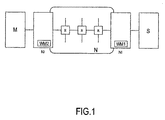
図1に、本発明によるネットワークオンチップの基本的な配置を示す。特に、各々がネットワークインターフェースNIに関連しているマスタモジュールMとスレーブモジュールSを示している。各モジュールMとSはそれぞれ、関連しているネットワークインターフェースNIを介してネットワークNに接続されている。ネットワークインターフェースNIは、マスタモジュールM及びスレーブモジュールSとネットワークNとの間のインターフェースとして用いられる。ネットワークインターフェースNIは、各モジュールM、SとネットワークNとの間の通信を管理するために設けられるため、各モジュールはネットワークまたは他のモジュールとの通信に対処する必要なく、それぞれの専用のオペレーションを実行することができる。ネットワークNは、一方のネットワークインターフェースNIから他方のネットワークインターフェースへ、ネットワークを通してデータをルーティングするための多数のネットワークルータRを具えることができる。 FIG. 1 shows a basic arrangement of a network on chip according to the present invention. In particular, a master module M and a slave module S, each associated with a network interface NI, are shown. Each module M and S is connected to a network N via an associated network interface NI. The network interface NI is used as an interface between the master module M and the slave module S and the network N. Since the network interface NI is provided to manage communication between the modules M and S and the network N, each module does not need to deal with communication with the network or other modules, and performs its dedicated operation. Can be executed. The network N can comprise a number of network routers R for routing data through the network from one network interface NI to the other network interface.
以下に説明するようなモジュールは、前記ネットワークインターフェースNIにてネットワークと情報をやり取りする、いわゆるインテレクチャル・プロパティ・ブロックIP(計算素子、メモリ、または、内部にインターコネクトモジュールを包含することができるサブシステム)とすることができる。ネットワークインターフェースNIは、1個またはそれ以上のIPブロックに接続することができる。同様に、IPブロックは1個以上のネットワークインターフェースNIに接続することができる。 The module described below exchanges information with the network through the network interface NI, and is a so-called intelligent property block IP (computing element, memory, or sub-module that can include an interconnect module therein). System). The network interface NI can be connected to one or more IP blocks. Similarly, an IP block can be connected to one or more network interfaces NI.
マスタモジュールM及びスレーブモジュールSに関連している各ネットワークインターフェースは、ラッパー(wrapper)手段WM2、WM1をそれぞれ具えている。ラッパー手段WM2、WM1は、ネットワークNを介してマスタM及びスレーブNから送信される任意のデータのバッファリングに関与する。特に、2個のラッパー手段WM1、WM2は、それぞれマスタMまたはスレーブSから到来するデータを、所定のデータ量がバッファされるまでバッファする。その後、バッファされたデータはネットワークN、すなわち、インターコネクトを介して、所定のバースト長内でパケットとして転送される。ラッパー手段WM2、WM1が、マスタM並びにスレーブSに関連して、要求並びに応答データをそれぞれのバースト長にてバッファ及び送信可能にすることに留意すべきである。応答が要求と異なることがあるように、それらのバースト長が異なることもある。選択バースト長は、ネットワークの利用性を改善するために、ネットワークNに適合するように選ばれなければならない。 Each network interface associated with the master module M and the slave module S comprises wrapper means WM2, WM1, respectively. The wrapper means WM2, WM1 are involved in buffering any data transmitted from the master M and slave N via the network N. In particular, the two wrapper means WM1, WM2 buffer data coming from the master M or slave S, respectively, until a predetermined amount of data is buffered. Thereafter, the buffered data is transferred as a packet within a predetermined burst length via the network N, that is, the interconnect. It should be noted that the wrapper means WM2, WM1 can buffer and transmit request and response data in the respective burst length in relation to the master M and the slave S. Their burst lengths can be different, as the response can be different from the request. The selected burst length must be chosen to match network N in order to improve network availability.
図2は、第2実施例によるネットワークオンチップの概略図を示す。特にこの第2実施例は、第1実施例によるネットワークオンチップにほぼ相当するものである。したがって、第1のラッパー手段WM1は、スレーブSに関連するネットワークインターフェースNI内に配置され、第2のラッパー手段WM2は、マスタMに関連するネットワークインターフェースNIの内部に配置されている。第1の実施例のように、ラッパー手段WM1、WM2は、最適な転送条件が満足されるまで、ネットワークNを介して送信すべきデータをバッファする働きをする。第1のアンバッファフラグユニットUBF1及び第2のバッファフラグユニットUBF2が、スレーブS及びマスタMにそれぞれ関連するネットワークインターフェースの内部に配置されている。第1及び第2のアンバッファフラグユニットUBF1、UBF2は、第1及び第2のアンバッファフラグを格納する働きをする。第1及び第2ラッパー手段は、第1または第2のアンバッファフラグが、第1または第2のアンバッファフラグユニットUBF1、UBF2内にそれぞれ設定されると、バッファされたデータを直ちに転送するように適合させる。こうしてバッファデータをフラッシュさせることにより、バッファされているデータがデッドロックされるのを防ぐことができる。このような場合、バッファされている全てのデータは、ネットワークNに対する最適なバースト長に適するパケットサイズになることを待たずに、できるだけ早く転送される。 FIG. 2 shows a schematic diagram of a network on chip according to a second embodiment. In particular, the second embodiment substantially corresponds to the network on chip according to the first embodiment. Accordingly, the first wrapper means WM1 is arranged in the network interface NI related to the slave S, and the second wrapper means WM2 is arranged inside the network interface NI related to the master M. As in the first embodiment, the wrapper means WM1, WM2 serve to buffer data to be transmitted via the network N until the optimum transfer conditions are satisfied. The first unbuffer flag unit UBF1 and the second buffer flag unit UBF2 are arranged inside the network interfaces associated with the slave S and the master M, respectively. The first and second unbuffer flag units UBF1, UBF2 serve to store the first and second unbuffer flags. The first and second wrapper means immediately transfer the buffered data when the first or second unbuffer flag is set in the first or second unbuffer flag unit UBF1, UBF2, respectively. To fit. By flushing the buffer data in this way, it is possible to prevent the buffered data from being deadlocked. In such a case, all buffered data is transferred as soon as possible without waiting for a packet size suitable for the optimum burst length for network N.
バッファされたデータのフラッシングは、第1または第2のラッパー手段WM1、WM2が受信する、第1または第2のアンバッファ信号によって達成することもできる。したがって、第1または第2のラッパー手段WM1、WM2がアンバッファ信号を受信した場合、現在バッファされているデータはできるだけ早く、すなわち、取得すべき最適なバースト長を待たずに転送される。その結果、マスタMは要求のフラッシングを開始することができ、スレーブSは応答のフラッシングを開始することができる。 The flushing of the buffered data can also be achieved by a first or second unbuffered signal received by the first or second wrapper means WM1, WM2. Thus, when the first or second wrapper means WM1, WM2 receives an unbuffered signal, the currently buffered data is transferred as soon as possible, ie without waiting for the optimum burst length to be acquired. As a result, the master M can start flushing requests, and the slave S can start flushing responses.
各トランザクションに対して与えられるアンバッファ信号とは対照的に、アンバッファフラグはやや長めの時間用に設定することができる。このようにして、バファリングの実行または停止を切り替えることができる。フラグは任意の方法、例えば、トランザクションの一部としてIPからの信号で、または、別のコンフィグレーションのトランザクション(特殊なフラッシュトランザクションか、または、メモリーマップ式の読取り及び書込み)を介して、設定/解除することができる。これらのトランザクションは、同一のIPからか、または別のコンフィグレーションのモジュールから送出することができる。 In contrast to the unbuffer signal provided for each transaction, the unbuffer flag can be set for a slightly longer time. In this way, execution or stop of buffering can be switched. The flag can be set / set in any way, eg as a signal from the IP as part of the transaction, or via another configuration transaction (special flash transaction or memory-mapped read and write). It can be canceled. These transactions can be sent from the same IP or from modules of different configurations.
さらに、第1及び第2の決定手段BLDU1、BLDU2が、スレーブS及びマスタMに関連するネットワークインターフェースNIの内部にそれぞれ配置されている。第1及び第2の決定ユニットBLDU1、BLDU2は、現在の通信またはコネクションのプロパティに従ってネットワークNを介してデータを転送するための、最適なバースト長を決定する働きをする。最適なバースト長は、要求された処理の初期段階の期間中、または所定の時間間隔の期間中に、静的または動的に決定することができる。あるいは、最適なバースト長は、(1)ネットワークを介してデータを転送するためのコネクションを設定する度に、(2)トランザクション毎に、(3)IPが他のコネクションに切り替わる度に、(4)パケット毎に、(5)ネットワークオンチップの状態が変化したとき(例えば、リコンフィギュレーション、NoC負荷、バッファの充填など)に動的に決定することもできる。最適なバースト長の決定は、決定ユニットBDLU1、2内に格納されている情報或いはネットワークNまたはIPブロックから受信される情報に基づいて行うことができる。したがって、ネットワークNは、要求された通信またはコネクションに対する通信若しくはコネクションのプロパティを決定すると共に、場合によっては格納するための、通信プロパティ手段CPMを具えることができる。CPMは、集中型または分散型(例えば、全てのNIの内部に)にすることができる。 Furthermore, first and second determination means BLDU1 and BLDU2 are arranged inside the network interface NI related to the slave S and the master M, respectively. The first and second decision units BLDU1, BLDU2 serve to determine the optimum burst length for transferring data via the network N according to the current communication or connection properties. The optimal burst length can be determined statically or dynamically during the initial stage of the requested processing or during a predetermined time interval. Alternatively, the optimum burst length is (1) every time a connection for transferring data via the network is set up, (2) every transaction, (3) every time the IP is switched to another connection, (4 It can also be determined dynamically for each packet (5) when the network on-chip state changes (eg, reconfiguration, NoC load, buffer filling, etc.). The optimum burst length can be determined based on information stored in the decision units BDLU1, 2 or information received from the network N or IP block. Thus, the network N may comprise a communication property means CPM for determining and possibly storing a communication or connection property for the requested communication or connection. CPM can be centralized or distributed (eg, within all NIs).
最適なバースト長の決定に加えて、伝送瞬時も、第1及び第2の決定手段BLDU1、BLDU2によって同様の方法で決定することができる。保証されたスループットのGTコネクションの場合、データは、そのコネクション用に確保されたスロットの1つを待たなければならない。「フラッシュ」のような信号/フラグを用いることによって、前もってデータを送信させることができる。さらに、ベストエフォートBE型のコネクションには、ネットワークインターフェースNIにおけるコネクション間のラウンドロビンアービトレーションを用いることができる。「フラッシュ」のような信号は、コネクションの優先度を一時的に高めにすることができる。 In addition to the determination of the optimum burst length, the transmission instant can also be determined in a similar manner by the first and second determination means BLDU1, BLDU2. In the case of a guaranteed throughput GT connection, the data must wait for one of the slots reserved for that connection. By using a signal / flag such as “flash”, data can be transmitted in advance. Furthermore, round-robin arbitration between connections in the network interface NI can be used for the best effort BE type connection. Signals such as “flash” can temporarily increase the priority of the connection.
第1及び第2実施例では、データ、すなわちバッファされるデータを、パケット形式でネットワークを介して送信する。パケットは、各ネットワークインターフェースNIにおいて形成するのが好適であり、ネットワークNに関しては最適な方法で転送するのに十分な大きさとしなければならない。全てのパケットはパケットヘッダを含むので、パケットが大きくなれば、必要とされるパケットヘッダの数が少なくなり、必然的にオーバーヘッドが低減され、ネットワークの利用性が改善される。データは、バッファされるデータがネットワークを介して転送できるような最適なパケットサイズに達するまでバッファされる。バッファされたデータ量が未だ最適なパケットサイズに達しない場合には、やや小さいサイズのパケットの転送が可能であったとしても、データはネットワークNを介して転送されることはない。バーストサイズは、バスまたは通信観点でのIPに関連付けられる一方で、パケット長は、パケット化が行われる(バスには不要)ときにのみ適用される。これ以前の段落にて記載した、バーストサイズを決定するスキームの全ては、最適なパケットサイズの決定に適用することもできる。 In the first and second embodiments, data, that is, buffered data, is transmitted through the network in a packet format. Packets are preferably formed at each network interface NI and should be large enough to be transferred in an optimal manner with respect to network N. Since all packets include a packet header, the larger the packet, the fewer the number of packet headers required, which inevitably reduces overhead and improves network usability. Data is buffered until the optimal packet size is reached so that the buffered data can be transferred over the network. If the buffered data amount still does not reach the optimum packet size, the data will not be transferred via the network N even if a slightly smaller packet can be transferred. While the burst size is associated with the bus or IP from a communication perspective, the packet length is only applied when packetization occurs (not required for the bus). All of the burst size determination schemes described in the previous paragraphs can also be applied to determine the optimal packet size.
第1及び第2実施例によれば、データはネットワークインターフェースNI、すなわち、インターコネクトインターフェース内にバッファされて、インテレクチャル・プロパティ・ブロックを構成し得るマスタMまたはスレーブSがインターコネクトまたはネットワークを介して通信するための実際の通信または通信プロトコルには関与しないようにするのが好適である。 According to the first and second embodiments, data is buffered in the network interface NI, i.e., the interconnect interface, and a master M or slave S, which can constitute an intelligent property block, is connected via the interconnect or network. It is preferred not to be involved in the actual communication or communication protocol for communication.
言い換えれば、バッファリングは、要求並びに応答に対して行うようにし、すなわち、要求並びに応答は、インターコネクトを介して転送する前に、マスタ及びスレーブ側のバッファにそれぞれ蓄積されるようにする。要求及び応答は、特定のインターコネクトにとって最適な長さのバーストで集められる。書込みのような要求があった場合には、トランザクションの応答部へのアンバッファフラグによってバッファリングを阻止することができる。したがって、保留中のもの及び現在のものを含む、全ての応答または要求は、インターコネクト用に最適なバースト長を形成するべくバッファされることなく、できるだけ早く転送される。 In other words, buffering is performed on requests and responses, that is, requests and responses are stored in buffers on the master and slave sides, respectively, before being transferred over the interconnect. Requests and responses are collected in bursts of an optimal length for a particular interconnect. When there is a request such as writing, buffering can be prevented by an unbuffer flag to the response part of the transaction. Thus, all responses or requests, including pending and current, are forwarded as soon as possible without being buffered to form an optimal burst length for the interconnect.
他の実施例によれば、マスタが、要求並びに応答のフラッシングを単独で、及び/または同時に開始し得るようにする。このような場合には、(AXIまたはDTL)コマンドグループは、異なる種類のフラッシュ(例えば、DTLにおける2ビットのフラッシュ信号)を指示できるように拡張させなければならない。応答フラッシングのこの指示は、この場合にそれ相応に動作するスレーブNIへと転送しなければならない。フラグを用いる場合にも同様なことが言える。 According to another embodiment, the master can initiate request and response flushing alone and / or simultaneously. In such cases, the (AXI or DTL) command group must be expanded to indicate different types of flash (eg, a 2-bit flash signal in DTL). This indication of response flushing must in this case be transferred to the slave NI operating accordingly. The same is true when using a flag.
さらに他の実施例によれば、ネットワークオンチップの通信スキームが、メッセージ通過通信スキームに基づくようにする。ここで、メッセージのメッセージヘッダは、フラッシュ情報を含むことができ、これにより、同一のコネクションから前もって送信された全てのメッセージをフラッシュさせる。 According to yet another embodiment, the network-on-chip communication scheme is based on a message passing communication scheme. Here, the message header of the message can include flush information, thereby flushing all messages previously transmitted from the same connection.
さらに他の実施例によれば、ネットワークオンチップの通信スキームを、パケットに基づく通信スキームとし、すなわち、1つのメッセージは1つまたはそれ以上のパケットにて送信され、フラッシュ情報はパケットヘッダ内に含まれるようにする。 According to yet another embodiment, the network-on-chip communication scheme is a packet-based communication scheme, i.e. one message is transmitted in one or more packets, and flush information is included in the packet header. To be.
上述したスキームは、DTLやAXIのような、トランザクションに基づくプロトコルにも適用することができる。特に、このスキームでは、ラッパーにインターコネクト用のバースト長を、要求だけでなく応答に対しても、トランザクション内で最適化することができるようにする。要求の例には(認知/非認知の)書込みコマンドとデータや、読取りコマンド、または、テスト兼設定、セマフォコマンド(P、V)のようなもっと複雑なコマンドがある。応答の例には、読取りデータ、書込み確認応答、及び、より複雑なコマンドからの応答がある。ラッパーまたはインターコネクトのインターフェースを介してインターコネクトに接続されるインテレクチュアル・プロパティ・モジュールは、インターコネクトに無関係に構築することができる。すなわち、インターコネクトの諸特性の知識はラッパー内にしかないので、これらIPモジュールの再利用性を増すことができる。しかしながら、要求に関しては、追加の待ち時間が導入されることになるが、システム全体の効率は向上する。 The scheme described above can also be applied to transaction-based protocols such as DTL and AXI. In particular, this scheme allows the wrapper burst length for the interconnect to be optimized within a transaction, not only for requests but also for responses. Examples of requests include write commands and data (acknowledged / unrecognized), read commands, or more complex commands such as test and set, semaphore commands (P, V). Examples of responses include read data, write confirmation responses, and responses from more complex commands. An intellectual property module connected to an interconnect via a wrapper or interconnect interface can be constructed independently of the interconnect. That is, since the knowledge of the characteristics of the interconnect is only in the wrapper, the reusability of these IP modules can be increased. However, with respect to requirements, additional latency will be introduced, but the overall system efficiency will be improved.
さらに、マスタ並びにスレーブに関連するネットワークインターフェースにラッパー手段を設けることによって、ネットワークインターフェースを対称的に設計することができるため、これらの再利用性も高まる。 Furthermore, by providing wrapper means for the network interfaces related to the master and the slave, the network interface can be designed symmetrically, so that their reusability is enhanced.
上述したそれぞれの実施例は本発明を制限するものではなく、当業者には、添付の請求項の範囲を逸脱することなく、多くの代替の実施例を設計し得ることに留意されたい。幾つかの手段を列挙している装置についての請求項において、それらの手段の幾つかは同一アイテムのハードウェアによっても実現することができる。所定の手段を互いに異なる従属項にて単に列挙していることは、それらの手段の組合せを有利に用いることができないということを示すものではない。 It should be noted that each of the above-described embodiments does not limit the present invention, and those skilled in the art can design many alternative embodiments without departing from the scope of the appended claims. In the device claim enumerating several means, several of these means can be embodied by one and the same item of hardware. The mere fact that certain measures are recited in mutually different dependent claims does not indicate that a combination of these measured cannot be used to advantage.
Claims (14)
第1の量のデータがバッファされるまで、インターコネクト手段を介して転送すべき前記第2の処理モジュールからのデータをバッファリングするように前記第2の処理モジュールに関連付けた第1のラッパー手段を具え、バッファされたデータは、前記第1の量のデータがバッファされたときに転送されるようにした、
ことを特徴とする集積回路。 An integrated circuit having a number of processing modules connected to interconnect means, wherein the first processing module communicates with a second processing module using transactions,
First wrapper means associated with the second processing module to buffer data from the second processing module to be transferred through the interconnect means until a first amount of data is buffered. The buffered data is transferred when the first amount of data is buffered,
An integrated circuit characterized by that.
ことを特徴とする請求項1に記載の集積回路。 Second wrapper means associated with the first processing module to buffer data from the first processing module to be transferred through the interconnect means until a second amount of data is buffered. Further, the buffered data is transferred when the second amount of data is buffered.
The integrated circuit according to claim 1.
ことを特徴とする請求項1または2に記載の集積回路。 First and second unbuffered signals or groups of signals, respectively, even if the amount of data buffered in the first and second wrapper means is less than the first and second amounts, respectively. Adapting the first and second wrapper means to transfer buffered data in response to a combination;
The integrated circuit according to claim 1 or 2, wherein
ことを特徴とする請求項1または2に記載の集積回路。 Even if the amount of data buffered in the first and second wrapper means is smaller than the first and second data amounts, the buffered data is transferred according to the first and second unbuffer flags, respectively. Adapting said first and second wrapper means to
The integrated circuit according to claim 1 or 2, wherein
ことを特徴とする請求項1または2に記載の集積回路。 A determination unit in which at least one of the first and second wrapper means determines an optimal first or second amount of data to be buffered according to the communication characteristics of the communication between the first and second processing modules. With
The integrated circuit according to claim 1 or 2, wherein
ことを特徴とする請求項1または2に記載の集積回路。 At least one of the first and second wrapper means determines an optimal instant to transmit the data of the first and second wrapper means according to the communication characteristics of the communication between the first and second processing modules. With a decision unit to
The integrated circuit according to claim 1 or 2, wherein
ことを特徴とする請求項3に記載の集積回路。 The first unbuffer signal is activated by the second processing module, and the second unbuffer signal is activated by the first processing module;
The integrated circuit according to claim 3.
ことを特徴とする請求項4に記載の集積回路。 The setting of the first unbuffer flag is started by the second processing module, and the setting of the second non-buffer flag is started by the first processing module.
The integrated circuit according to claim 4.
ことを特徴とする請求項3または4に記載の集積回路。 Adapting the first processing module to activate the first and / or the second unbuffered signal;
The integrated circuit according to claim 3 or 4, wherein
ことを特徴とする請求項4に記載の集積回路。 Adapting the first processing module to begin setting the first and / or the second unbuffer flag;
The integrated circuit according to claim 4.
前記第1及び第2のラッパー手段にバッファされたデータの量が、前記第1及び第2の量より少なくても、前記メッセージヘッダにおける情報に応答して、バッファされたデータを転送するように前記第1及び第2のラッパー手段をそれぞれ適合させた、
ことを特徴とする請求項1または2に記載の集積回路。 The first and second processing modules communicate with each other using a message transfer communication scheme, and the message includes a message header;
The buffered data is transferred in response to the information in the message header even if the amount of data buffered in the first and second wrapper means is less than the first and second amounts. Each of the first and second wrapper means adapted;
The integrated circuit according to claim 1 or 2, wherein
前記第1及び第2のラッパー手段にバッファされたデータの量が、前記第1及び第2の量より少なくても、前記パケットヘッダにおける情報に応答して、バッファされたデータを転送するように前記第1及び第2のラッパー手段をそれぞれ適合させた、
ことを特徴とする請求項1または2に記載の集積回路。 The first and second processing modules communicate with each other using a packet-based communication scheme, the packet including a packet header;
In order to transfer the buffered data in response to the information in the packet header, even if the amount of data buffered in the first and second wrapper means is less than the first and second amounts. Each of the first and second wrapper means adapted;
The integrated circuit according to claim 1 or 2, wherein
第1の量のデータがバッファされるまで、インターコネクト手段を介して転送すべき前記第2の処理モジュールからのデータをバッファリングし、バッファされたデータは、前記第1の量のデータがバッファされたときに転送するステップを含む、
ことを特徴とするバッファリング方法。 A method of buffering data in an integrated circuit having a number of processing modules connected to interconnect means, wherein the first processing module communicates with a second processing module using transactions.
Buffer the data from the second processing module to be transferred through the interconnect means until the first amount of data is buffered, and the buffered data is buffered with the first amount of data. Including the step of forwarding when
And a buffering method.
第1の量のデータがバッファされるまで、インターコネクト手段を介して転送すべき前記第2の処理モジュールからのデータをバッファリングするように前記第2の処理モジュールに関連付けた第1のラッパー手段を具え、バッファされたデータは、前記第1の量のデータがバッファされたときに転送されるようにした、
ことを特徴とするデータ処理システム。 A data processing system comprising a number of processing modules connected to interconnect means, wherein the first processing module communicates with a second processing module using transactions,
First wrapper means associated with the second processing module to buffer data from the second processing module to be transferred through the interconnect means until a first amount of data is buffered. The buffered data is transferred when the first amount of data is buffered,
A data processing system characterized by that.
Applications Claiming Priority (2)
| Application Number | Priority Date | Filing Date | Title |
|---|---|---|---|
| EP04102189 | 2004-05-18 | ||
| PCT/IB2005/051580 WO2005111823A1 (en) | 2004-05-18 | 2005-05-13 | Integrated circuit and method for buffering to optimize burst length in networks on chips |
Publications (1)
| Publication Number | Publication Date |
|---|---|
| JP2007538331A true JP2007538331A (en) | 2007-12-27 |
Family
ID=34967297
Family Applications (1)
| Application Number | Title | Priority Date | Filing Date |
|---|---|---|---|
| JP2007517554A Pending JP2007538331A (en) | 2004-05-18 | 2005-05-13 | Integrated circuit and buffering method |
Country Status (7)
| Country | Link |
|---|---|
| US (1) | US8086800B2 (en) |
| EP (1) | EP1751667B1 (en) |
| JP (1) | JP2007538331A (en) |
| CN (1) | CN100445977C (en) |
| AT (1) | ATE396454T1 (en) |
| DE (1) | DE602005007014D1 (en) |
| WO (1) | WO2005111823A1 (en) |
Families Citing this family (15)
| Publication number | Priority date | Publication date | Assignee | Title |
|---|---|---|---|---|
| US8254913B2 (en) | 2005-08-18 | 2012-08-28 | Smartsky Networks LLC | Terrestrial based high speed data communications mesh network |
| KR100653087B1 (en) * | 2005-10-17 | 2006-12-01 | 삼성전자주식회사 | System for axi compatible network on chip and interleaving method thereof |
| EP1791366A1 (en) * | 2005-11-28 | 2007-05-30 | Alcatel Lucent | Avoiding interruptions in the reproduction of audio/video by storing enough data in advance at a mobile terminal |
| US8261025B2 (en) | 2007-11-12 | 2012-09-04 | International Business Machines Corporation | Software pipelining on a network on chip |
| EP2063581A1 (en) * | 2007-11-20 | 2009-05-27 | STMicroelectronics (Grenoble) SAS | Transferring a stream of data between first and second electronic devices via a network on-chip |
| US8526422B2 (en) | 2007-11-27 | 2013-09-03 | International Business Machines Corporation | Network on chip with partitions |
| US8490110B2 (en) * | 2008-02-15 | 2013-07-16 | International Business Machines Corporation | Network on chip with a low latency, high bandwidth application messaging interconnect |
| US8423715B2 (en) | 2008-05-01 | 2013-04-16 | International Business Machines Corporation | Memory management among levels of cache in a memory hierarchy |
| US8494833B2 (en) | 2008-05-09 | 2013-07-23 | International Business Machines Corporation | Emulating a computer run time environment |
| US8392664B2 (en) | 2008-05-09 | 2013-03-05 | International Business Machines Corporation | Network on chip |
| US8438578B2 (en) | 2008-06-09 | 2013-05-07 | International Business Machines Corporation | Network on chip with an I/O accelerator |
| US8195884B2 (en) | 2008-09-18 | 2012-06-05 | International Business Machines Corporation | Network on chip with caching restrictions for pages of computer memory |
| US9110668B2 (en) * | 2012-01-31 | 2015-08-18 | Broadcom Corporation | Enhanced buffer-batch management for energy efficient networking based on a power mode of a network interface |
| US10983910B2 (en) * | 2018-02-22 | 2021-04-20 | Netspeed Systems, Inc. | Bandwidth weighting mechanism based network-on-chip (NoC) configuration |
| US11782865B1 (en) * | 2021-06-02 | 2023-10-10 | Amazon Technologies, Inc. | Flexible data handling |
Citations (4)
| Publication number | Priority date | Publication date | Assignee | Title |
|---|---|---|---|---|
| JPH07123118A (en) * | 1993-10-21 | 1995-05-12 | Fuji Xerox Co Ltd | Frame transmission circuit |
| JP2000209652A (en) * | 1999-01-18 | 2000-07-28 | Kobe Steel Ltd | Radiotelephony system |
| JP2002084289A (en) * | 2000-09-07 | 2002-03-22 | Kddi Corp | Tcp communication method |
| WO2004034173A2 (en) * | 2002-10-08 | 2004-04-22 | Koninklijke Philips Electronics N.V. | Integrated circuit and method for exchanging data |
Family Cites Families (14)
| Publication number | Priority date | Publication date | Assignee | Title |
|---|---|---|---|---|
| US4228496A (en) * | 1976-09-07 | 1980-10-14 | Tandem Computers Incorporated | Multiprocessor system |
| US4253144A (en) * | 1978-12-21 | 1981-02-24 | Burroughs Corporation | Multi-processor communication network |
| US5522050A (en) * | 1993-05-28 | 1996-05-28 | International Business Machines Corporation | Bus-to-bus bridge for a multiple bus information handling system that optimizes data transfers between a system bus and a peripheral bus |
| US5987552A (en) * | 1998-01-26 | 1999-11-16 | Intel Corporation | Bus protocol for atomic transactions |
| US6397287B1 (en) * | 1999-01-27 | 2002-05-28 | 3Com Corporation | Method and apparatus for dynamic bus request and burst-length control |
| US6493776B1 (en) * | 1999-08-12 | 2002-12-10 | Mips Technologies, Inc. | Scalable on-chip system bus |
| US6393500B1 (en) * | 1999-08-12 | 2002-05-21 | Mips Technologies, Inc. | Burst-configurable data bus |
| US6629253B1 (en) * | 1999-12-30 | 2003-09-30 | Intel Corporation | System for efficient management of memory access requests from a planar video overlay data stream using a time delay |
| US6668308B2 (en) * | 2000-06-10 | 2003-12-23 | Hewlett-Packard Development Company, L.P. | Scalable architecture based on single-chip multiprocessing |
| GB2373595B (en) * | 2001-03-15 | 2005-09-07 | Italtel Spa | A system of distributed microprocessor interfaces toward macro-cell based designs implemented as ASIC or FPGA bread boarding and relative common bus protocol |
| US7012893B2 (en) * | 2001-06-12 | 2006-03-14 | Smartpackets, Inc. | Adaptive control of data packet size in networks |
| GB0315504D0 (en) * | 2003-07-02 | 2003-08-06 | Advanced Risc Mach Ltd | Coherent multi-processing system |
| JP4729490B2 (en) | 2003-09-04 | 2011-07-20 | コーニンクレッカ フィリップス エレクトロニクス エヌ ヴィ | Data processing system |
| US7257665B2 (en) * | 2003-09-29 | 2007-08-14 | Intel Corporation | Branch-aware FIFO for interprocessor data sharing |
-
2005
- 2005-05-13 WO PCT/IB2005/051580 patent/WO2005111823A1/en active IP Right Grant
- 2005-05-13 JP JP2007517554A patent/JP2007538331A/en active Pending
- 2005-05-13 AT AT05739743T patent/ATE396454T1/en not_active IP Right Cessation
- 2005-05-13 CN CNB2005800158550A patent/CN100445977C/en not_active Expired - Fee Related
- 2005-05-13 DE DE602005007014T patent/DE602005007014D1/en active Active
- 2005-05-13 EP EP05739743A patent/EP1751667B1/en not_active Not-in-force
- 2005-05-13 US US11/569,083 patent/US8086800B2/en active Active
Patent Citations (4)
| Publication number | Priority date | Publication date | Assignee | Title |
|---|---|---|---|---|
| JPH07123118A (en) * | 1993-10-21 | 1995-05-12 | Fuji Xerox Co Ltd | Frame transmission circuit |
| JP2000209652A (en) * | 1999-01-18 | 2000-07-28 | Kobe Steel Ltd | Radiotelephony system |
| JP2002084289A (en) * | 2000-09-07 | 2002-03-22 | Kddi Corp | Tcp communication method |
| WO2004034173A2 (en) * | 2002-10-08 | 2004-04-22 | Koninklijke Philips Electronics N.V. | Integrated circuit and method for exchanging data |
Also Published As
| Publication number | Publication date |
|---|---|
| ATE396454T1 (en) | 2008-06-15 |
| US20070226407A1 (en) | 2007-09-27 |
| CN100445977C (en) | 2008-12-24 |
| WO2005111823A1 (en) | 2005-11-24 |
| EP1751667B1 (en) | 2008-05-21 |
| CN1954306A (en) | 2007-04-25 |
| US8086800B2 (en) | 2011-12-27 |
| DE602005007014D1 (en) | 2008-07-03 |
| EP1751667A1 (en) | 2007-02-14 |
Similar Documents
| Publication | Publication Date | Title |
|---|---|---|
| JP2007538331A (en) | Integrated circuit and buffering method | |
| US7594052B2 (en) | Integrated circuit and method of communication service mapping | |
| US8285912B2 (en) | Communication infrastructure for a data processing apparatus and a method of operation of such a communication infrastructure | |
| KR100687659B1 (en) | Network interface of controlling lock operation in accordance with axi protocol, packet data communication on-chip interconnect system of including the network interface, and method of operating the network interface | |
| EP1552669B1 (en) | Integrated circuit and method for establishing transactions | |
| US7613849B2 (en) | Integrated circuit and method for transaction abortion | |
| US8014401B2 (en) | Electronic device and method of communication resource allocation | |
| KR101699784B1 (en) | Bus system and operating method thereof | |
| JP2004525449A (en) | Interconnect system | |
| US20080043757A1 (en) | Integrated Circuit And Method For Packet Switching Control | |
| US7978693B2 (en) | Integrated circuit and method for packet switching control | |
| US7917728B2 (en) | Integrated circuit and method for transaction retraction | |
| JP2008520119A (en) | Electronic device and communication resource allocation method | |
| JP5007337B2 (en) | Control of power consumption in data processing equipment. | |
| US20070245044A1 (en) | System of interconnections for external functional blocks on a chip provided with a single configurable communication protocol | |
| JP5146454B2 (en) | Information processing apparatus and information processing method | |
| CN101594291B (en) | Unblock network system and subgroup arbitration method thereof |
Legal Events
| Date | Code | Title | Description |
|---|---|---|---|
| A621 | Written request for application examination |
Free format text: JAPANESE INTERMEDIATE CODE: A621 Effective date: 20080512 |
|
| RD02 | Notification of acceptance of power of attorney |
Free format text: JAPANESE INTERMEDIATE CODE: A7422 Effective date: 20080904 |
|
| A977 | Report on retrieval |
Free format text: JAPANESE INTERMEDIATE CODE: A971007 Effective date: 20110114 |
|
| A131 | Notification of reasons for refusal |
Free format text: JAPANESE INTERMEDIATE CODE: A131 Effective date: 20110125 |
|
| A521 | Request for written amendment filed |
Free format text: JAPANESE INTERMEDIATE CODE: A523 Effective date: 20110425 |
|
| A02 | Decision of refusal |
Free format text: JAPANESE INTERMEDIATE CODE: A02 Effective date: 20110802 |