JP2007257543A - Composite portable electronic equipment and composite ic card - Google Patents
Composite portable electronic equipment and composite ic card Download PDFInfo
- Publication number
- JP2007257543A JP2007257543A JP2006084058A JP2006084058A JP2007257543A JP 2007257543 A JP2007257543 A JP 2007257543A JP 2006084058 A JP2006084058 A JP 2006084058A JP 2006084058 A JP2006084058 A JP 2006084058A JP 2007257543 A JP2007257543 A JP 2007257543A
- Authority
- JP
- Japan
- Prior art keywords
- contact
- interface
- contact interface
- external device
- composite
- Prior art date
- Legal status (The legal status is an assumption and is not a legal conclusion. Google has not performed a legal analysis and makes no representation as to the accuracy of the status listed.)
- Pending
Links
Images

Abstract
Description
本発明は、たとえば、接触式インタフェイスおよび非接触式インタフェイスをそれぞれ有し、これら接触式インタフェイスあるいは非接触式インタフェイスにより、接触式インタフェイスおよび非接触式インタフェイスをそれぞれ備えた外部装置(カードリーダ・ライタ)と通信を行なう複合ICカード(いわゆる、コンビカード)と称される複合携帯可能電子装置および複合ICカードに関する。 The present invention includes, for example, an external device having a contact interface and a non-contact interface, respectively, and each of the contact interface and the non-contact interface includes the contact interface and the non-contact interface. The present invention relates to a composite portable electronic device called a composite IC card (so-called combination card) and a composite IC card that communicate with a (card reader / writer).
この種の複合ICカードとして、メモリおよびCPU(セントラル・プロセッシング・ユニット)を有するとともに、外部装置からの入力に応答して新たな信号を発生するICチップを備え、外部装置と接触して応答するための電気的接点機構(接触式インタフェイス)と、外部装置と非接触で無線通信により応答するためのアンテナ機構(非接触式インタフェイス)とを併設したものが公知である(たとえば、特許文献1参照)。 This type of composite IC card includes a memory and a CPU (Central Processing Unit), and an IC chip that generates a new signal in response to an input from an external device, and responds by contacting the external device. And an antenna mechanism (non-contact type interface) for responding by wireless communication in a non-contact manner with an external device are well known (for example, patent documents) 1).
この複合ICカードは、電気的接点機構に接続した外部装置によりメモリの内容の書込みや書換えが可能であり、外部装置と非接触で無線通信により応答する場合には、メモリ内の特定情報を変調してアンテナ機構から外部装置へ出力するように構成されている。 This IC card can be written and rewritten to the memory by an external device connected to the electrical contact mechanism. When responding by wireless communication without contact with the external device, specific information in the memory is modulated. Thus, the antenna mechanism is configured to output to an external device.
このような複合ICカードにおける外部装置(リーダ・ライタ)との通信制御に関する公知技術として、最初に確立した通信方式(インタフェイス)で通信を開始し、その後は他の通信方式(他方のインタフェイス)の動作を許可しないようにしたものがある(たとえば、特許文献2参照)。
しかしながら、接触式インタフェイスを用いた通信でのデータ通信速度は、非接触式インタフェイスを用いた通信に比べて遅く、大容量のデータ通信には適さない。
また、セキュリティ性の高いデータ通信においては、外乱ノイズの影響等を受けやすい非接触式インタフェイスによる通信では適さない。
However, the data communication speed in the communication using the contact type interface is slower than the communication using the non-contact type interface, and is not suitable for large-capacity data communication.
In addition, data communication with high security is not suitable for communication using a non-contact interface that is easily affected by disturbance noise.
そこで、本発明は、外部装置からのコマンドを非接触式インタフェイスで受信し、当該コマンドに対するレスポンスを接触式インタフェイスで外部装置へ送信し、あるいは、外部装置からのコマンドを接触式インタフェイスで受信し、当該コマンドに対するレスポンスは非接触式インタフェイスで外部装置へ送信することで、たとえば、セキュリティ性の高いデータを付加して送信されるコマンドは接触式インタフェイスにて確実に送信することができ、また、大容量のデータを含むコマンドは非接触式インタフェイスにて高速伝送により送信することができる複合携帯可能電子装置および複合ICカードを提供することを目的とする。 Therefore, the present invention receives a command from an external device via a non-contact interface and transmits a response to the command to the external device via a contact interface, or sends a command from the external device via a contact interface. By receiving and sending a response to the command to the external device through a non-contact interface, for example, a command transmitted with high security data added can be reliably transmitted through the contact interface. Further, it is an object to provide a composite portable electronic device and a composite IC card that can transmit a command including a large amount of data by high-speed transmission through a non-contact interface.
本発明の複合携帯可能電子装置は、接触式インタフェイスおよび非接触式インタフェイスをそれぞれ有し、これら接触式インタフェイスあるいは非接触式インタフェイスにより、接触式インタフェイスおよび非接触式インタフェイスをそれぞれ有する外部装置と通信を行なう複合携帯可能電子装置において、前記外部装置から非接触式インタフェイスにより送信されるコマンドを前記非接触式インタフェイスにより受信し、この受信したコマンドに対するレスポンスを前記接触式インタフェイスにより前記外部装置へ送信する第1の通信手段と、前記外部装置から接触式インタフェイスにより送信されるコマンドを前記接触式インタフェイスにより受信し、この受信したコマンドに対するレスポンスを前記非接触式インタフェイスにより前記外部装置へ送信する第2の通信手段と、これら第1、第2の通信手段のいずれか一方を選択する選択手段とを具備している。 The composite portable electronic device of the present invention has a contact type interface and a non-contact type interface, respectively, and a contact type interface and a non-contact type interface are respectively provided by the contact type interface or the non-contact type interface. In a composite portable electronic device that communicates with an external device, the command transmitted from the external device via a non-contact interface is received by the non-contact interface, and a response to the received command is received by the contact interface. A first communication means for transmitting to the external device by a face; a command transmitted from the external device by a contact interface; and a response to the received command as a response to the received command. Said by face A second communication means for transmitting to the part unit, these first, and a selection means for selecting one of the second communication means.
また、本発明の複合ICカードは、接触式インタフェイスおよび非接触式インタフェイスをそれぞれ有し、これら接触式インタフェイスあるいは非接触式インタフェイスにより、接触式インタフェイスおよび非接触式インタフェイスをそれぞれ有する外部装置と通信を行なう複合ICカードにおいて、前記外部装置から非接触式インタフェイスにより送信されるコマンドを前記非接触式インタフェイスにより受信し、この受信したコマンドに対するレスポンスを前記接触式インタフェイスにより前記外部装置へ送信する第1の通信手段と、前記外部装置から接触式インタフェイスにより送信されるコマンドを前記接触式インタフェイスにより受信し、この受信したコマンドに対するレスポンスを前記非接触式インタフェイスにより前記外部装置へ送信する第2の通信手段と、これら第1、第2の通信手段のいずれか一方を選択する選択手段とを有したICモジュールと、このICモジュールを収納したICカード本体とを具備している。 Further, the composite IC card of the present invention has a contact interface and a non-contact interface, respectively, and a contact interface and a non-contact interface are respectively provided by the contact interface or the non-contact interface. In a composite IC card that communicates with an external device having, a command transmitted from the external device by a non-contact interface is received by the non-contact interface, and a response to the received command is received by the contact interface. A first communication means for transmitting to the external device and a command transmitted from the external device through a contact interface are received by the contact interface, and a response to the received command is received by the non-contact interface. External packaging An IC module having a second communication means for transmitting to the terminal, a selection means for selecting one of the first and second communication means, and an IC card main body containing the IC module. Yes.
本発明によれば、外部装置からのコマンドを非接触式インタフェイスで受信し、当該コマンドに対するレスポンスを接触式インタフェイスで外部装置へ送信し、あるいは、外部装置からのコマンドを接触式インタフェイスで受信し、当該コマンドに対するレスポンスは非接触式インタフェイスで外部装置へ送信することで、たとえば、セキュリティ性の高いデータを付加して送信されるコマンドは接触式インタフェイスにて確実に送信することができ、また、大容量のデータを含むコマンドは非接触式インタフェイスにて高速伝送により送信することができる複合携帯可能電子装置および複合ICカードを提供できる。 According to the present invention, a command from an external device is received by a non-contact interface, and a response to the command is transmitted to the external device by a contact interface, or a command from the external device is transmitted by a contact interface. By receiving and sending a response to the command to the external device through a non-contact interface, for example, a command transmitted with high security data added can be reliably transmitted through the contact interface. In addition, it is possible to provide a composite portable electronic device and a composite IC card in which a command including a large amount of data can be transmitted by high-speed transmission through a contactless interface.
以下、本発明の実施の形態について図面を参照して説明する。
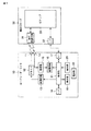
図1は、本発明の実施の形態に係る複合携帯可能電子装置としての複合ICカード(いわゆる、コンビカード)を取扱う複合ICカードシステムの構成を示すものである。この複合ICカードシステムは、接触式インタフェイスおよび非接触式インタフェイスをそれぞれ備えた兼用のカードリーダ・ライタ(外部装置)10と、接触式インタフェイスおよび非接触式インタフェイスをそれぞれ有する複合ICカード30とに大別される。
Embodiments of the present invention will be described below with reference to the drawings.
FIG. 1 shows a configuration of a composite IC card system that handles a composite IC card (so-called combination card) as a composite portable electronic device according to an embodiment of the present invention. This composite IC card system includes a combined card reader / writer (external device) 10 having a contact interface and a non-contact interface, and a composite IC card having a contact interface and a non-contact interface, respectively. 30.
カードリーダ・ライタ10は、複合ICカード30に対するデータの読出し、書込み(記憶)コマンドの送信、読出しデータの処理、書込みデータの送信などを行なうもので、送信アンテナ11、送信用のドライバ12、変調回路13、受信アンテナ14、受信用の増幅器15、復調回路16、複合ICカード30と接続される接触式インタフェイスとしてのコンタクト部17、図示しない上位装置と接続されるインタフェイス部18、表示部19、キーボードなどの操作部20、これら全体の制御を司るCPUなどからなる制御部21、および、これら各部に動作電源を供給する電源部22などによって構成されている。
The card reader /
複合ICカード30は、カードリーダ・ライタ10からのコマンドの解読、データの書込み(記憶)、レスポンス(データ)の送信などを行なうもので、送受信アンテナとしてのループ状のアンテナコイルと同調コンデンサ(いずれも図示しない)とからなる並列同調回路31、カードリーダ・ライタ10のコンタクト部17と接続される接触式インタフェイスとしてのコンタクト部32、および、これら並列同調回路31およびコンタクト部32が接続されたICチップ33などによって構成されている。
The
並列同調回路31は、非接触式インタフェイスとして機能し、非接触式インタフェイスによる通信を実行する場合に用いられるもので、たとえば、図2および図3に示すように、ICカード本体30a内に埋設されたループ状のアンテナコイル31aおよび同調コンデンサ31bにより構成されている。
The
コンタクト部32は、接触式インタフェイスによる通信を実行する場合に用いられるもので、たとえば、図2および図3に示すように、カードリーダ・ライタ10のコンタクト部17と接触して応答するための電気的接点機構となる6個の接触端子C1〜C6を備えていて、これら接触端子C1〜C6はICカード本体30aの表面に露出した状態で形成されている。
The
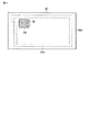
すなわち、図2および図3に示すように、ICカード本体30aの表面にコンタクト部32としての接触端子C1(電源端子(VDD))、C2(リセット端子(RST))、C3(クロック端子(CLK))、C4(接地端子(GND))、C5(入出力端子(I/O))、C6(予備端子)が接触式インタフェイスとして配置されている。 That is, as shown in FIG. 2 and FIG. 3, contact terminals C1 (power supply terminal (VDD)), C2 (reset terminal (RST)), C3 (clock terminal (CLK) )), C4 (ground terminal (GND)), C5 (input / output terminal (I / O)), and C6 (spare terminal) are arranged as contact-type interfaces.
ICチップ33は、たとえば、図3に示すように、並列同調回路31に接続された整流回路(ダイオードブリッジ回路)41、整流回路41の出力に接続されたレギュレータ42、レギュレータ42の出力電圧を検知する電圧検知回路43、電源選択用のNPNトランジスタ44、リセット信号を発生するリセット回路45、各種処理や制御を行なう制御ロジック回路46、送信信号変調用のFETトランジスタ47、リセット信号切換回路48、クロック信号切換回路49、受信信号切換回路50、送信信号切換回路51、送受信切換回路52、および、排他的論理和回路53などを有して構成される。
For example, as shown in FIG. 3, the
制御ロジック回路46は、電源生成部、復調回路、制御用のCPU、CPUの制御プログラム等を記憶するROM、データ一時記憶用のRAM、および、各種データなどが記憶されるEEPROM等の不揮発性メモリなどを有して構成される。
The
ICチップ33は1つの基板上に設けられていて、各接触端子C1〜C6とは配線により接続されているとともに、各接触端子C1〜C6とICチップ33を搭載した基板とは一体化され、ICモジュール34としてハンドリングされることにより、図2に示すように、ICカード本体30aの表面に各接触端子C1〜C6が露出するようにICカード本体30a内に埋設されている。
The
以下、このような構成において複合ICカード30の基本動作について説明する。なお、通信インタフェイスの初期設定は接触式インタフェイスが選択されるものとする。
並列同調回路31は所定の周波数fに共振していて、カードリーダ・ライタ10からの電波(送信キャリア)をアンテナコイル31aが受信すると、その受信信号が整流回路41にて全波整流され、整流回路41の出力端41aには直流電圧が生成される。レギュレータ42は、整流回路41の出力電圧が所定値以上にならないように安定化制御を行なう。
Hereinafter, the basic operation of the
The
電圧検知回路43は、レギュレータ42の出力電圧と、あらかじめ設定されている基準電圧Vrefとの比較を行ない、基準電圧Vrefの方が高い場合はローレベル信号(“L”)を出力し、レギュレータ42の出力電圧の方が高い場合はハイレベル信号(“H”)を出力する。
The
電圧検知回路43の出力にハイレベル信号が出力されると、電圧検知回路43の出力により制御されるトランジスタ44がオン状態となり、非接触式インタフェイスにて生成された電源電圧、すなわちレギュレータ42の出力電圧が電源電圧VDDとして選択され、制御ロジック回路46に送られる。
When a high level signal is output to the output of the
電圧検知回路43の出力信号は、接触式インタフェイスからの信号と、非接触式インタフェイスからの信号とを切換える制御信号であり、ローレベル信号の場合は接触式インタフェイスが選択され、ハイレベル信号の場合は非接触式インタフェイスが選択される。
The output signal of the
リセット回路45は、レギュレータ42の出力電圧を入力とし、レギュレータ42の出力電圧があらかじめ定められた所定値以上になったことを検知したタイミングから一定時間後にローレベル(“L”)からハイレベル(“H”)に変化するロジックレベル信号を出力する。この信号は、制御ロジック回路46内のロジック回路のリセット信号RSTとして入力される。
The
いま、非接触式インタフェイスが選択されている場合、電圧検知回路43の出力信号はハイレベルである。
これにより、電圧検知回路43の出力により制御されるリセット信号切換回路48は、電圧検知回路43の出力信号がハイレベルであるため、リセット回路45の出力を選択し、リセット信号RSTとして制御ロジック回路46に供給される。
Now, when the non-contact interface is selected, the output signal of the
Thereby, the reset
また、電圧検知回路43の出力により制御されるクロック信号切換回路49は、電圧検知回路43の出力信号がハイレベルであるため、並列同調回路31からの受信信号を選択し、2値化された信号がクロック信号CLKとして制御ロジック回路46に供給される。
Further, the clock signal switching circuit 49 controlled by the output of the
また、電圧検知回路43の出力により制御される受信信号切換回路50は、電圧検知回路43の出力信号がハイレベルであるため、整流回路41の出力端41aからの信号を選択し、検波された変調信号が受信信号RXとして制御ロジック回路46に供給される。
The reception
排他的論理和回路53の出力により制御される送信信号切換回路51は、排他的論理和回路53の出力信号がハイレベルであるため、制御ロジック回路46からの送信信号TXを選択する。これにより、送信信号TXを入力とするトランジスタ47のスイッチング動作により、電流ドライブでの変調波信号として並列同調回路31のアンテナコイル31aから出力される。
The transmission
次に、接触式インタフェイスが選択されている場合、電圧検知回路43の出力信号はローレベルである。
これにより、電圧検知回路43の出力により制御されるリセット信号切換回路48は、電圧検知回路43の出力信号がローレベルであるため、コンタクト部32のリセット端子C2からの信号を選択し、リセット信号RSTとして制御ロジック回路46に供給される。
Next, when the contact type interface is selected, the output signal of the
Thereby, the reset
また、電圧検知回路43の出力により制御されるクロック信号切換回路49は、電圧検知回路43の出力信号がローレベルであるため、コンタクト部32のクロック端子C3からの信号を選択し、クロック信号CLKとして制御ロジック回路46に供給される。
The clock signal switching circuit 49 controlled by the output of the
接触式インタフェイスが選択される場合、コンタクト部32の入出力端子C5が送信、受信の機能を果たすため、受信モードの場合、制御ロジック回路46は入出力制御信号I/O−CNTをハイレベルにすることで、送受信切換回路52は、入出力端子C5からの受信信号を選択し、受信信号RXとして制御ロジック回路46に供給される。
When the contact type interface is selected, the input / output terminal C5 of the
また、送信モードの場合、制御ロジック回路46は入出力制御信号I/O−CNTをローレベルにすることで、送受信切換回路52は、制御ロジック回路46からの送信信号TXを選択し、コンタクト部32の入出力端子C5に供給する。
In the transmission mode, the
次に、カードリーダ・ライタ10から非接触式インタフェイスでコマンドを受信したとき、当該コマンドに対するレスポンスを接触式インタフェイスでカードリーダ・ライタ10へ送信する場合について説明する。
Next, when a command is received from the card reader /
通常、非接触式インタフェイスが選択されている場合、電圧検知回路43の出力はハイレベルである。また、制御ロジック回路46からのモード信号MODOは通常、ローレベルを出力している。これにより、電圧検知回路43の出力およびモード信号MODOを入力とする排他的論理和回路53は、出力信号がハイレベルである。したがって、排他的論理和回路53の出力により制御される送信信号切換回路51は、非接触式インタフェイスを選択し、非接触式インタフェイスでレスポンスが送信される。
Normally, when the non-contact type interface is selected, the output of the
これに対し、モード信号MODOをハイレベルにした場合、排他的論理和回路53の出力はローレベルとなり、送信信号切換回路51は接触式インタフェイスを選択し、接触式インタフェイス(コンタクト部32)でレスポンスが送信される。
On the other hand, when the mode signal MODEO is set to the high level, the output of the exclusive OR circuit 53 becomes the low level, the transmission
次に、カードリーダ・ライタ10から接触式インタフェイスでコマンドを受信したとき、当該コマンドに対するレスポンスを非接触式インタフェイスでカードリーダ・ライタ10へ送信する場合について説明する。
Next, when a command is received from the card reader /
通常、接触式インタフェイスが選択されている場合、電圧検知回路43の出力はローレベルである。また、制御ロジック回路46からのモード信号MODOは通常、ローレベルを出力している。これにより、電圧検知回路43の出力およびモード信号MODOを入力とする排他的論理和回路53は、出力信号がハイレベルである。したがって、排他的論理和回路53の出力により制御される送信信号切換回路51は、接触式インタフェイスを選択し、接触式インタフェイスでレスポンスが送信される。
Normally, when the contact type interface is selected, the output of the
これに対し、モード信号MODOをハイレベルにした場合、排他的論理和回路53の出力はハイレベルとなり、送信信号切換回路51は非接触式インタフェイスを選択し、非接触式インタフェイスでレスポンスが送信される。
On the other hand, when the mode signal MODEO is set to the high level, the output of the exclusive OR circuit 53 is set to the high level, the transmission
このように、接触式インタフェイスおよび非接触式インタフェイスをそれぞれ有する複合ICカードにおいて、カードリーダ・ライタからのコマンドを非接触式インタフェイスで受信し、当該コマンドに対するレスポンスを接触式インタフェイスでカードリーダ・ライタへ送信し、あるいは、カードリーダ・ライタからのコマンドを接触式インタフェイスで受信し、当該コマンドに対するレスポンスは非接触式インタフェイスでカードリーダ・ライタへ送信することで、たとえば、セキュリティ性の高いデータを付加して送信されるコマンドは接触式インタフェイスにて確実に送信することができ、また、大容量のデータを含むコマンドは非接触式インタフェイスにて高速伝送により送信することができ、通信性能の向上も図れる。
また、接触式インタフェイスと非接触式インタフェイスを自在に切換え可能とすることにより、多種のカードリーダ・ライタとの互換性が向上する。
As described above, in a composite IC card having a contact interface and a contactless interface, a command from the card reader / writer is received by the contactless interface, and a response to the command is received by the contact interface card. Sending to a reader / writer or receiving a command from a card reader / writer via a contact interface, and sending a response to the command to the card reader / writer via a non-contact interface. Commands that are transmitted with high data can be transmitted reliably with a contact interface, and commands containing large amounts of data can be transmitted at high speed with a non-contact interface. Communication performance can be improved.
In addition, compatibility with various card readers / writers is improved by enabling switching between a contact interface and a non-contact interface.
なお、カードリーダ・ライタ10と複合ICカード30との間で通信を行なっている際に通信エラーが発生した場合には、エラーが発生した際のインタフェイスとは異なるインタフェイスでカードリーダ・ライタ10に対しエラー発生を告知してもよい。
When a communication error occurs during communication between the card reader /
また、前記実施の形態では、複合ICカードに適用した場合について説明したが、本発明はこれに限定されるものでなく、たとえば、PDAと称される携帯情報端末装置や携帯電話機等、接触式インタフェイスによる通信および非接触式インタフェイスによる通信の双方の機能を備えた複合携帯可能電子装置であれば適用できる。 In the above embodiment, the case where the present invention is applied to a composite IC card has been described. However, the present invention is not limited to this, and for example, a portable information terminal device called PDA, a mobile phone, etc. The present invention can be applied to any composite portable electronic device having functions of both communication by an interface and communication by a non-contact interface.
10…カードリーダ・ライタ(外部装置)、30…複合ICカード(複合携帯可能電子装置)、30a…ICカード本体、11…送信アンテナ、12…送信用のドライバ、13…変調回路、14…受信アンテナ、16…復調回路、17…コンタクト部(接触式インタフェイス)、21…制御部、31…並列同調回路、31a…アンテナコイル、31b…同調コンデンサ、32…コンタクト部(接触式インタフェイス)、33…ICチップ、34…ICモジュール、41…整流回路、42…レギュレータ、43…電圧検知回路、44…NPNトランジスタ、45…リセット回路、46…制御ロジック回路、47…トランジスタ、48…リセット信号切換回路、49…クロック信号切換回路、50…受信信号切換回路、51…送信信号切換回路、52…送受信切換回路、53…排他的論理和回路。
DESCRIPTION OF
Claims (8)
前記外部装置から非接触式インタフェイスにより送信されるコマンドを前記非接触式インタフェイスにより受信し、この受信したコマンドに対するレスポンスを前記接触式インタフェイスにより前記外部装置へ送信する第1の通信手段と、
前記外部装置から接触式インタフェイスにより送信されるコマンドを前記接触式インタフェイスにより受信し、この受信したコマンドに対するレスポンスを前記非接触式インタフェイスにより前記外部装置へ送信する第2の通信手段と、
これら第1、第2の通信手段のいずれか一方を選択する選択手段と、
を具備したことを特徴とする複合携帯可能電子装置。 It has a contact interface and a non-contact type interface, and these contact type interface or non-contact type interface enables to communicate with external devices having contact type and non-contact type interfaces respectively. In electronic devices,
A first communication means for receiving a command transmitted from the external device through a non-contact interface through the non-contact interface and transmitting a response to the received command to the external device through the contact interface; ,
A second communication means for receiving a command transmitted from the external device through a contact interface through the contact interface, and transmitting a response to the received command to the external device through the non-contact interface;
Selection means for selecting one of the first and second communication means;
A composite portable electronic device comprising:
前記外部装置から非接触式インタフェイスを介して送信されるコマンドに対するレスポンスを前記接触式インタフェイスを介して前記外部装置へ送信する通信手段を具備したことを特徴とする複合携帯可能電子装置。 It has a contact interface and a non-contact type interface, and these contact type interface or non-contact type interface enables to communicate with external devices having contact type and non-contact type interfaces respectively. In electronic devices,
A composite portable electronic device comprising a communication unit that transmits a response to a command transmitted from the external device via a non-contact interface to the external device via the contact interface.
前記外部装置から接触式インタフェイスを介して送信されるコマンドに対するレスポンスを前記非接触式インタフェイスを介して前記外部装置へ送信する通信手段を具備したことを特徴とする複合携帯可能電子装置。 It has a contact interface and a non-contact type interface, and these contact type interface or non-contact type interface enables to communicate with external devices having contact type and non-contact type interfaces respectively. In electronic devices,
A composite portable electronic device comprising: a communication unit that transmits a response to a command transmitted from the external device via a contact interface to the external device via the non-contact interface.
前記外部装置から非接触式インタフェイスにより送信されるコマンドを前記非接触式インタフェイスにより受信し、この受信したコマンドに対するレスポンスを前記接触式インタフェイスにより前記外部装置へ送信する第1の通信手段と、前記外部装置から接触式インタフェイスにより送信されるコマンドを前記接触式インタフェイスにより受信し、この受信したコマンドに対するレスポンスを前記非接触式インタフェイスにより前記外部装置へ送信する第2の通信手段と、これら第1、第2の通信手段のいずれか一方を選択する選択手段とを有したICモジュールと、
このICモジュールを収納したICカード本体と、
を具備したことを特徴とする複合ICカード。 A composite IC card having a contact interface and a non-contact interface, and communicating with an external device having the contact interface and the non-contact interface through the contact interface or the non-contact interface, respectively. In
A first communication means for receiving a command transmitted from the external device through a non-contact interface through the non-contact interface and transmitting a response to the received command to the external device through the contact interface; A second communication means for receiving a command transmitted from the external device via the contact interface via the contact interface and transmitting a response to the received command to the external device via the non-contact interface; An IC module having selection means for selecting any one of the first and second communication means;
An IC card body containing the IC module;
A composite IC card characterized by comprising:
前記外部装置から非接触式インタフェイスを介して送信されるコマンドに対するレスポンスを前記接触式インタフェイスを介して前記外部装置へ送信する通信手段を有したICモジュールと、
このICモジュールを収納したICカード本体と、
を具備したことを特徴とする複合ICカード。 A composite IC card having a contact interface and a non-contact interface, and communicating with an external device having the contact interface and the non-contact interface through the contact interface or the non-contact interface, respectively. In
An IC module having communication means for transmitting a response to a command transmitted from the external device via a non-contact interface to the external device via the contact interface;
An IC card body containing the IC module;
A composite IC card characterized by comprising:
前記外部装置から接触式インタフェイスを介して送信されるコマンドに対するレスポンスを前記非接触式インタフェイスを介して前記外部装置へ送信する通信手段を有したICモジュールと、
このICモジュールを収納したICカード本体と、
を具備したことを特徴とする複合ICカード。 A composite IC card having a contact interface and a non-contact interface, and communicating with an external device having the contact interface and the non-contact interface through the contact interface or the non-contact interface, respectively. In
An IC module having communication means for transmitting a response to a command transmitted from the external device via the contact interface to the external device via the non-contact interface;
An IC card body containing the IC module;
A composite IC card characterized by comprising:
Priority Applications (1)
| Application Number | Priority Date | Filing Date | Title |
|---|---|---|---|
| JP2006084058A JP2007257543A (en) | 2006-03-24 | 2006-03-24 | Composite portable electronic equipment and composite ic card |
Applications Claiming Priority (1)
| Application Number | Priority Date | Filing Date | Title |
|---|---|---|---|
| JP2006084058A JP2007257543A (en) | 2006-03-24 | 2006-03-24 | Composite portable electronic equipment and composite ic card |
Publications (1)
| Publication Number | Publication Date |
|---|---|
| JP2007257543A true JP2007257543A (en) | 2007-10-04 |
Family
ID=38631688
Family Applications (1)
| Application Number | Title | Priority Date | Filing Date |
|---|---|---|---|
| JP2006084058A Pending JP2007257543A (en) | 2006-03-24 | 2006-03-24 | Composite portable electronic equipment and composite ic card |
Country Status (1)
| Country | Link |
|---|---|
| JP (1) | JP2007257543A (en) |
Cited By (3)
| Publication number | Priority date | Publication date | Assignee | Title |
|---|---|---|---|---|
| JP2016057824A (en) * | 2014-09-09 | 2016-04-21 | 株式会社東芝 | Ic card, ic module and portable terminal |
| US9679236B2 (en) | 2014-09-09 | 2017-06-13 | Kabushiki Kaisha Toshiba | IC card, portable terminal, and portable electronic apparatus |
| CN113519006A (en) * | 2019-07-03 | 2021-10-19 | 第一资本服务有限责任公司 | Techniques for performing applet programming |
Citations (2)
| Publication number | Priority date | Publication date | Assignee | Title |
|---|---|---|---|---|
| JPH07282212A (en) * | 1994-04-07 | 1995-10-27 | Kobe Steel Ltd | Noncontact ic card |
| JP2003132313A (en) * | 2001-10-24 | 2003-05-09 | Toshiba Corp | Lsi for combination card, combination card, and using method for combination card |
-
2006
- 2006-03-24 JP JP2006084058A patent/JP2007257543A/en active Pending
Patent Citations (2)
| Publication number | Priority date | Publication date | Assignee | Title |
|---|---|---|---|---|
| JPH07282212A (en) * | 1994-04-07 | 1995-10-27 | Kobe Steel Ltd | Noncontact ic card |
| JP2003132313A (en) * | 2001-10-24 | 2003-05-09 | Toshiba Corp | Lsi for combination card, combination card, and using method for combination card |
Cited By (8)
| Publication number | Priority date | Publication date | Assignee | Title |
|---|---|---|---|---|
| JP2016057824A (en) * | 2014-09-09 | 2016-04-21 | 株式会社東芝 | Ic card, ic module and portable terminal |
| US9679236B2 (en) | 2014-09-09 | 2017-06-13 | Kabushiki Kaisha Toshiba | IC card, portable terminal, and portable electronic apparatus |
| KR101814253B1 (en) * | 2014-09-09 | 2018-01-30 | 가부시끼가이샤 도시바 | Ic card and portable terminal |
| KR101825326B1 (en) | 2014-09-09 | 2018-02-02 | 가부시끼가이샤 도시바 | Portable electronic device |
| US10032105B2 (en) | 2014-09-09 | 2018-07-24 | Kabushiki Kaisha Toshiba | IC card, portable terminal, and portable electronic apparatus |
| US10360490B2 (en) | 2014-09-09 | 2019-07-23 | Kabushiki Kaisha Toshiba | IC card, portable terminal, and portable electronic apparatus |
| CN113519006A (en) * | 2019-07-03 | 2021-10-19 | 第一资本服务有限责任公司 | Techniques for performing applet programming |
| JP2022538423A (en) * | 2019-07-03 | 2022-09-02 | キャピタル・ワン・サービシーズ・リミテッド・ライアビリティ・カンパニー | Techniques for performing applet programming |
Similar Documents
| Publication | Publication Date | Title |
|---|---|---|
| TWI534712B (en) | Smartcard performance enhancement circuits and systems | |
| US8643470B2 (en) | Semiconductor integrated circuit, IC card mounted with the semiconductor integrated circuit, and operation method for the same | |
| US7403122B1 (en) | RFID tag circuits operable at different speeds | |
| US20070237087A1 (en) | Communication medium, communication medium processing apparatus, and communication medium processing system | |
| US9536118B2 (en) | Card reader and method of operating the same | |
| JP2008536431A (en) | Improved transponder | |
| US10032105B2 (en) | IC card, portable terminal, and portable electronic apparatus | |
| JP2007094597A (en) | Ic tag, ic tag system, and command execution method | |
| US20070069865A1 (en) | IC tag, IC tag system, and data communicating method for the IC tag | |
| JP3929761B2 (en) | Semiconductor device operation control method, semiconductor device operation control program, recording medium recording semiconductor device operation control program, semiconductor device, and IC card | |
| US20100064152A1 (en) | Ic chip, information processing device, information processing system, and programs | |
| JP2007257543A (en) | Composite portable electronic equipment and composite ic card | |
| US20120234926A1 (en) | Portable electronic apparatus | |
| JP2008028852A (en) | Information processing terminal, data selection processing method, and program | |
| JP2011239180A (en) | Non-contact communication medium reading data converter | |
| JP2000322544A (en) | Portable electronic device | |
| JP7366765B2 (en) | Control program for IC cards, IC card processing systems, and IC card processing devices | |
| JP7433886B2 (en) | IC cards and IC card control programs | |
| JP2008276572A (en) | Non-contact ic card | |
| JP5481464B2 (en) | Communication medium and communication medium processing apparatus | |
| JP2001283164A (en) | Transmitting and receiving system and transmitting and receiving device and reader/writer system and responding device and non-contact ic card and label tag | |
| JP2012027667A (en) | Portable electronic device, ic card, and control method for portable electronic device | |
| JP2010198208A (en) | Contactless portable electronic device and contactless ic card | |
| JP2009296061A (en) | Information processor, communication method and program | |
| JP2007122451A (en) | Communication medium and communication medium processor |
Legal Events
| Date | Code | Title | Description |
|---|---|---|---|
| A621 | Written request for application examination |
Free format text: JAPANESE INTERMEDIATE CODE: A621 Effective date: 20080918 |
|
| A977 | Report on retrieval |
Free format text: JAPANESE INTERMEDIATE CODE: A971007 Effective date: 20111026 |
|
| A131 | Notification of reasons for refusal |
Free format text: JAPANESE INTERMEDIATE CODE: A131 Effective date: 20111115 |
|
| A02 | Decision of refusal |
Free format text: JAPANESE INTERMEDIATE CODE: A02 Effective date: 20120313 |