JP2007166350A - Gate array program unit, measurement unit, and program - Google Patents
Gate array program unit, measurement unit, and program Download PDFInfo
- Publication number
- JP2007166350A JP2007166350A JP2005361205A JP2005361205A JP2007166350A JP 2007166350 A JP2007166350 A JP 2007166350A JP 2005361205 A JP2005361205 A JP 2005361205A JP 2005361205 A JP2005361205 A JP 2005361205A JP 2007166350 A JP2007166350 A JP 2007166350A
- Authority
- JP
- Japan
- Prior art keywords
- pseudo
- noise code
- noise
- gate array
- code
- Prior art date
- Legal status (The legal status is an assumption and is not a legal conclusion. Google has not performed a legal analysis and makes no representation as to the accuracy of the status listed.)
- Pending
Links
Images
Classifications
-
- H—ELECTRICITY
- H04—ELECTRIC COMMUNICATION TECHNIQUE
- H04J—MULTIPLEX COMMUNICATION
- H04J13/00—Code division multiplex systems
-
- H—ELECTRICITY
- H04—ELECTRIC COMMUNICATION TECHNIQUE
- H04B—TRANSMISSION
- H04B1/00—Details of transmission systems, not covered by a single one of groups H04B3/00 - H04B13/00; Details of transmission systems not characterised by the medium used for transmission
- H04B1/69—Spread spectrum techniques
- H04B1/707—Spread spectrum techniques using direct sequence modulation
- H04B1/7073—Synchronisation aspects
- H04B1/7075—Synchronisation aspects with code phase acquisition
-
- H—ELECTRICITY
- H04—ELECTRIC COMMUNICATION TECHNIQUE
- H04J—MULTIPLEX COMMUNICATION
- H04J13/00—Code division multiplex systems
- H04J13/0007—Code type
- H04J13/0022—PN, e.g. Kronecker
-
- H—ELECTRICITY
- H04—ELECTRIC COMMUNICATION TECHNIQUE
- H04J—MULTIPLEX COMMUNICATION
- H04J13/00—Code division multiplex systems
- H04J13/10—Code generation
Abstract
Description
本発明は、CDMA装置に係り、特に同期捕捉機能を有するCDMA装置に関する。 The present invention relates to a CDMA device, and more particularly to a CDMA device having a synchronization acquisition function.
W−CDMA方式の携帯電話機や基地局など、直接拡散方式のCDMA受信機は、受信信号を復調するために、受信信号の拡散符号と同期する必要がある。同期方法の代表的なものとしては、直列的に演算処理するスライディング相関器(Sliding Correlator)を用いる方法や並列的に演算処理するマッチトフィルタ(Matched Filter)を用いる方法がある(例えば、特許文献1〜5および非特許文献1〜5を参照。)。これらの方法による同期は、受信ベースバンド信号の拡散符号の位相(タイミング)と受信機内で生成された拡散符号の位相とが一致する時に、受信機内で生成した拡散符号と受信ベースバンド信号との相関値が最大になることを利用している。 A direct-spreading CDMA receiver, such as a W-CDMA mobile phone or base station, needs to synchronize with the spreading code of the received signal in order to demodulate the received signal. Typical examples of the synchronization method include a method using a sliding correlator that performs serial arithmetic processing and a method that uses a matched filter that performs arithmetic processing in parallel (for example, Patent Documents). 1-5 and non-patent documents 1-5.) Synchronization by these methods is performed when the phase (timing) of the spread code of the received baseband signal matches the phase of the spread code generated in the receiver, and the spread code generated in the receiver and the received baseband signal are synchronized. It takes advantage of the maximum correlation value.
CDMA方式の信号を測定するディジタル受信機や測定装置は、ASICやFPGAなどのゲートアレイで同期捕捉装置や復調装置を構成して、当該ゲートアレイに被測定信号を処理させる。特に、測定装置は、基地局や携帯電話機に比べて市場に出回る数が少なく、また、基地局や携帯電話機と異なり汎用性が求められるので、FPGAで構成されることが多い。ところで、ゲートアレイの設計の途中段階において、同期捕捉に許される処理時間や同期捕捉における相関長に変更が生じる場合がある。あるいは、既存の製品またはプラットフォームを流用して、新しいCDMA方式に対応した装置を開発する場合がある。これらの場合、ゲートアレイは、使用できるリソース数や動作クロック周波数が概ねあるいは完全に決まっている。一般に、スライディング相関器は、相関処理に必要な乗算器および加算器がそれぞれ1つずつあれば足りる一方、同期捕捉に要する時間が長い。また、マッチトフィルタは、高速に同期捕捉を行える一方、膨大な数の乗算器および加算器を必要とする。従って、上記のような変更に対応しようとすると、所望の仕様の同期捕捉装置が使用予定のゲートアレイにうまく適合せず、ゲートアレイそのものの変更やゲートアレイの動作クロック周波数の変更を余儀なくされる場合があって、設計効率が悪い。そこで、所望の仕様の同期捕捉装置をゲートアレイ内に実現するにあたり、ゲートアレイ・リソースの所要数やゲートアレイの動作クロック周波数を従来に比べて柔軟に選択できる同期捕捉装置の提供が望まれている。また、測定装置は、同期捕捉装置や復調装置だけでなく、測定に必要な装置も同一ゲートアレイで構成される場合が多い。近年、測定装置において、同時にできるだけ多くの項目の測定を実施することが期待されており、ゲートアレイ内に実現される各装置のリソース消費の低減が望まれている。 A digital receiver or a measurement device that measures a CDMA signal includes a gate array such as an ASIC or FPGA that forms a synchronization acquisition device or a demodulation device, and causes the gate array to process a signal under measurement. In particular, the number of measurement devices that are on the market is smaller than that of base stations and mobile phones, and, unlike base stations and mobile phones, versatility is required. By the way, in the middle stage of the gate array design, there are cases where the processing time allowed for synchronization acquisition and the correlation length in synchronization acquisition are changed. Alternatively, an existing product or platform may be used to develop a device that supports a new CDMA system. In these cases, the number of usable resources and the operating clock frequency of the gate array are almost or completely determined. In general, a sliding correlator is only required to have one multiplier and one adder each required for correlation processing, but takes a long time to acquire synchronization. In addition, the matched filter can perform synchronous acquisition at high speed, but requires a large number of multipliers and adders. Therefore, when trying to cope with such a change as described above, the synchronous acquisition device having a desired specification is not well adapted to the gate array to be used, and the gate array itself or the operation clock frequency of the gate array must be changed. In some cases, design efficiency is poor. Therefore, it is desired to provide a synchronization acquisition device that can flexibly select the required number of gate array resources and the operation clock frequency of the gate array when realizing a synchronization acquisition device of a desired specification in the gate array. Yes. In many cases, not only the synchronization acquisition device and the demodulation device but also the devices necessary for the measurement are configured by the same gate array. In recent years, it has been expected that measurement devices can simultaneously measure as many items as possible, and it is desired to reduce the resource consumption of each device implemented in the gate array.
本発明は、上記の課題を解決するために為されたものである。すなわち、本第一の発明は、測定装置に具備される再構成可能なゲートアレイをプログラムする装置であって、前記ゲートアレイを、被測定信号に含まれる第一の疑似雑音符号と同じ符号系列であって、それぞれ位相が異なるK個の第二の疑似雑音符号を発生する疑似雑音符号発生器と、前記K個のうち2以上のM個の前記第二の疑似雑音符号を選択対象とし、選択対象の前記第二の疑似雑音符号から1つを選択して出力する2以上のN個のセレクタであって、あるセレクタが選択対象とする前記第二の疑似雑音符号がその他のセレクタの選択対象外であるセレクタと、各前記セレクタに個々に接続されるN個の乗算器であって、対応する前記セレクタが出力する前記第二の疑似雑音符号と前記第一の疑似雑音符号とを乗ずる乗算器と、各前記乗算器に個々に接続されるN個の加算器であって、対応する前記乗算器が出力する乗算結果を前記乗算結果に対応する前記第二の疑似雑音符号の位相ごとに累積加算する加算器と、前記加算器の加算結果のうち絶対値が最大である加算結果または所定閾値を超える加算結果に対応する前記第二の疑似雑音符号の位相を、前記第一の疑似雑音符号の位相として検出する検出器、として機能するようにプログラムし、各前記セレクタが、対応する前記乗算器に前記第一の疑似雑音符号の同一チップデータが供給されている間に、選択対象の前記第二の疑似雑音符号の全てが前記対応する乗算器に供給されるように、前記第二の疑似雑音符号を選択し、前記測定装置が前記第一の疑似雑音符号に同期できるようにすることを特徴とするものである。 The present invention has been made to solve the above-described problems. That is, the first invention is an apparatus for programming a reconfigurable gate array provided in a measuring apparatus, and the gate array is the same code sequence as the first pseudo-noise code included in the signal under measurement. A pseudo-noise code generator that generates K second pseudo-noise codes each having a different phase, and two or more M second pseudo-noise codes out of the K are selected. Two or more N selectors that select and output one of the second pseudo-noise codes to be selected, and the second pseudo-noise code to be selected by a selector is selected by another selector A selector that is not a target, and N multipliers individually connected to each of the selectors, which are multiplied by the second pseudo-noise code output by the corresponding selector. Multiplier and each front N adders individually connected to the multiplier, the adders for cumulatively adding the multiplication results output from the corresponding multipliers for each phase of the second pseudo-noise code corresponding to the multiplication results And detecting the phase of the second pseudo noise code corresponding to the addition result having the maximum absolute value or the addition result exceeding a predetermined threshold among the addition results of the adder as the phase of the first pseudo noise code Each of the selectors while the same chip data of the first pseudo-noise code is being supplied to the corresponding multiplier. Selecting the second pseudo-noise code so that all of the noise code is supplied to the corresponding multiplier, so that the measuring device can be synchronized with the first pseudo-noise code. Is a thing
また、本第二の発明は、被測定信号を格納する記憶装置を備える測定装置に具備され、前記被測定信号のチップレートよりも速いクロックで動作する再構成可能なゲートアレイをプログラムする装置であって、前記ゲートアレイを、前記被測定信号に含まれる第一の疑似雑音符号と同じ符号系列であって、それぞれ位相が異なるK個の第二の疑似雑音符号を発生する疑似雑音符号発生器と、前記K個のうち2以上のM個の前記第二の疑似雑音符号を選択対象とし、選択対象の前記第二の疑似雑音符号から1つを選択して出力する2以上のN個のセレクタであって、あるセレクタが選択対象とする前記第二の疑似雑音符号がその他のセレクタの選択対象外であるセレクタと、各前記セレクタに個々に接続されるN個の乗算器であって、対応する前記セレクタが出力する前記第二の疑似雑音符号と前記記憶装置から読み出される前記被測定信号に含まれる前記第一の疑似雑音符号とを乗ずる乗算器と、各前記乗算器に個々に接続されるN個の加算器であって、対応する前記乗算器が出力する乗算結果を前記乗算結果に対応する前記第二の疑似雑音符号の位相ごとに累積加算する加算器と、前記加算器の加算結果のうち絶対値が最大である加算結果または所定閾値を超える加算結果に対応する前記第二の疑似雑音符号の位相を、前記第一の疑似雑音符号の位相として検出する検出器、として機能するようにプログラムし、各前記セレクタが、対応する前記乗算器に前記第一の疑似雑音符号の同一チップデータが供給されている間に、選択対象の前記第二の疑似雑音符号の全てが前記対応する乗算器に供給されるように、前記第二の疑似雑音符号を選択し、前記測定装置が前記第一の疑似雑音符号に同期できるようにすることを特徴とするものである。 The second invention is an apparatus for programming a reconfigurable gate array that is provided in a measuring apparatus having a storage device for storing a signal under measurement and that operates at a clock faster than the chip rate of the signal under measurement. A pseudo-noise code generator for generating K second pseudo-noise codes having the same code sequence as the first pseudo-noise code included in the signal under measurement and having different phases, And two or more M of the K second pseudo-noise codes are selected, and one or more of the second pseudo-noise codes to be selected are selected and output. A selector in which the second pseudo-noise code to be selected by a selector is not selected by other selectors, and N multipliers individually connected to each of the selectors, Corresponding A multiplier that multiplies the second pseudo-noise code output from the selector and the first pseudo-noise code included in the signal under measurement read from the storage device, and is individually connected to each of the multipliers. N adders that cumulatively add the multiplication results output from the corresponding multipliers for each phase of the second pseudo-noise code corresponding to the multiplication results; and the addition results of the adders The phase of the second pseudo noise code corresponding to the addition result having the maximum absolute value or the addition result exceeding the predetermined threshold value as a detector that detects the phase of the first pseudo noise code. Each of the selectors is supplied with the same chip data of the first pseudo-noise code to the corresponding multiplier. As will be supplied to the multiplier, and selects the second pseudo-noise code, and is characterized in that the measuring device is to be synchronized with the first pseudo-noise code.
さらに、本第三の発明は、本第一の発明または本第二の発明の装置において、各前記セレクタが、固定された順序およびタイミングで周期的に繰り返し前記第二の疑似雑音符号を選択し、各前記加算器が、対応する前記セレクタにおける前記第二の疑似雑音符号の選択周期と等しい時間遅延を有する第一の遅延器を用いて累積加算を行うことを特徴とするものである。 Further, according to the third invention, in the device of the first invention or the second invention, each selector repeatedly selects the second pseudo-noise code periodically in a fixed order and timing. Each of the adders performs cumulative addition using a first delay unit having a time delay equal to the selection period of the second pseudo-noise code in the corresponding selector.
またさらに、本第四の発明は、本第一の発明乃至本第三の発明のいずれかの装置において、前記疑似雑音符号発生器が、前記第一の疑似雑音符号と同じ符号系列を有する単一の第三の疑似雑音符号を基に、複数の第二の遅延器を介して、前記第二の疑似雑音符号の全てを並列的に発生することを特徴とするものである。 Still further, according to a fourth aspect of the present invention, in the apparatus according to any one of the first to third aspects of the present invention, the pseudo noise code generator has a code sequence that is the same as the first pseudo noise code. All of the second pseudo noise codes are generated in parallel through a plurality of second delay devices based on one third pseudo noise code.
また、本第五の発明は、本第四の発明の装置において、前記第三の疑似雑音符号が、前記ゲートアレイ内の記憶領域に予め格納された疑似雑音符号であることを特徴とするものである。 According to a fifth aspect of the invention, in the apparatus of the fourth aspect of the invention, the third pseudo noise code is a pseudo noise code stored in advance in a storage area in the gate array. It is.
さらに、本第六の発明は、本第一の発明乃至本第五の発明のいずれかの装置において、前記Mおよび前記Nのそれぞれが、前記ゲートアレイのプログラム毎に異なる値を有しうることを特徴とするものである。 Furthermore, according to the sixth aspect of the present invention, in the apparatus according to any one of the first to fifth aspects of the present invention, each of the M and the N may have a different value for each program of the gate array. It is characterized by.
またさらに、本第七の発明は、再構成可能なゲートアレイを具備する測定装置であって、前記ゲートアレイが、被測定信号に含まれる第一の疑似雑音符号と同じ符号系列であって、それぞれ位相が異なるK個の第二の疑似雑音符号を発生する疑似雑音符号発生器と、前記K個のうち2以上のM個の前記第二の疑似雑音符号を選択対象とし、選択対象の前記第二の疑似雑音符号から1つを選択して出力する2以上のN個のセレクタであって、あるセレクタが選択対象とする前記第二の疑似雑音符号がその他のセレクタの選択対象外であるセレクタと、各前記セレクタに個々に接続されるN個の乗算器であって、対応する前記セレクタが出力する前記第二の疑似雑音符号と前記第一の疑似雑音符号とを乗ずる乗算器と、各前記乗算器に個々に接続されるN個の加算器であって、対応する前記乗算器が出力する乗算結果を前記乗算結果に対応する前記第二の疑似雑音符号の位相ごとに累積加算する加算器と、前記加算器の加算結果のうち絶対値が最大である加算結果または所定閾値を超える加算結果に対応する前記第二の疑似雑音符号の位相を、前記第一の疑似雑音符号の位相として検出する検出器、として機能するようにプログラムされ、各前記セレクタが、対応する前記乗算器に前記第一の疑似雑音符号の同一チップデータが供給されている間に、選択対象の前記第二の疑似雑音符号の全てが前記対応する乗算器に供給されるように、前記第二の疑似雑音符号を選択し、前記測定装置が前記第一の疑似雑音符号に同期できるようにしたことを特徴とするものである。 Still further, the seventh invention is a measurement apparatus comprising a reconfigurable gate array, wherein the gate array is the same code sequence as the first pseudo-noise code included in the signal under measurement, A pseudo-noise code generator that generates K second pseudo-noise codes each having a different phase, and two or more M second pseudo-noise codes out of the K are selected, and the selection target Two or more N selectors that select and output one of the second pseudo-noise codes, and the second pseudo-noise code that is selected by a certain selector is not selected by other selectors A selector, and N multipliers individually connected to each of the selectors, the multiplier multiplying the second pseudo noise code output from the corresponding selector, and the first pseudo noise code; Individually connected to each said multiplier An adder for cumulatively adding the multiplication results output from the corresponding multipliers for each phase of the second pseudo-noise code corresponding to the multiplication results, and adding the adders It functions as a detector that detects the phase of the second pseudo noise code corresponding to the addition result having the maximum absolute value or the addition result exceeding a predetermined threshold as the phase of the first pseudo noise code. Each of the selectors is supplied with the same chip data of the first pseudo-noise code to the corresponding multiplier. The second pseudo-noise code is selected so as to be supplied to the multiplier, and the measurement device can synchronize with the first pseudo-noise code.
また、本第八の発明は、被測定信号を格納する記憶装置と、前記被測定信号のチップレートよりも速いクロックで動作する再構成可能なゲートアレイとを備える測定装置であって、前記ゲートアレイが、前記被測定信号に含まれる第一の疑似雑音符号と同じ符号系列であって、それぞれ位相が異なるK個の第二の疑似雑音符号を発生する疑似雑音符号発生器と、前記K個のうち2以上のM個の前記第二の疑似雑音符号を選択対象とし、選択対象の前記第二の疑似雑音符号から1つを選択して出力する2以上のN個のセレクタであって、あるセレクタが選択対象とする前記第二の疑似雑音符号がその他のセレクタの選択対象外であるセレクタと、各前記セレクタに個々に接続されるN個の乗算器であって、対応する前記セレクタが出力する前記第二の疑似雑音符号と前記記憶装置から読み出される前記被測定信号に含まれる前記第一の疑似雑音符号とを乗ずる乗算器と、各前記乗算器に個々に接続されるN個の加算器であって、対応する前記乗算器が出力する乗算結果を前記乗算結果に対応する前記第二の疑似雑音符号の位相ごとに累積加算する加算器と、前記加算器の加算結果のうち絶対値が最大である加算結果または所定閾値を超える加算結果に対応する前記第二の疑似雑音符号の位相を、前記第一の疑似雑音符号の位相として検出する検出器、として機能するようにプログラムされ、各前記セレクタが、対応する前記乗算器に前記第一の疑似雑音符号の同一チップデータが供給されている間に、選択対象の前記第二の疑似雑音符号の全てが前記対応する乗算器に供給されるように、前記第二の疑似雑音符号を選択し、前記測定装置が前記第一の疑似雑音符号に同期できるようにしたことを特徴とするものである。 The eighth invention is a measuring apparatus comprising a storage device for storing a signal under measurement and a reconfigurable gate array that operates at a clock faster than a chip rate of the signal under measurement. A pseudo-noise code generator for generating K second pseudo-noise codes, the array of which is the same code sequence as the first pseudo-noise code included in the signal under measurement, each having a different phase; Two or more N selectors that select and output one or more of the second pseudo-noise codes that are two or more of the second pseudo-noise codes, A selector in which the second pseudo-noise code to be selected by a selector is not selected by other selectors, and N multipliers individually connected to each of the selectors, wherein the corresponding selector To output A multiplier that multiplies the second pseudo-noise code and the first pseudo-noise code included in the signal under measurement read from the storage device, and N adders individually connected to the multipliers. An adder that cumulatively adds the multiplication results output from the corresponding multipliers for each phase of the second pseudo-noise code corresponding to the multiplication results, and the absolute value of the addition results of the adders is the maximum. Each of the selectors is programmed to function as a detector that detects a phase of the second pseudo-noise code corresponding to a certain addition result or an addition result exceeding a predetermined threshold as the phase of the first pseudo-noise code. However, while the same chip data of the first pseudo-noise code is supplied to the corresponding multiplier, all the second pseudo-noise codes to be selected are supplied to the corresponding multiplier. , It selects the second pseudo-noise code, and is characterized in that the measuring device has to be synchronized with the first pseudo-noise code.
さらに、本第九の発明は、本第七の発明または本第八の発明の装置において、各前記セレクタが、固定された順序およびタイミングで周期的に繰り返し前記第二の疑似雑音符号を選択し、各前記加算器が、対応する前記セレクタにおける前記第二の疑似雑音符号の選択周期と等しい時間遅延を有する第一の遅延器を用いて累積加算を行うことを特徴とするものである。 Furthermore, the ninth invention is the apparatus of the seventh invention or the eighth invention, wherein each of the selectors selects the second pseudo noise code periodically and repeatedly in a fixed order and timing. Each of the adders performs cumulative addition using a first delay unit having a time delay equal to the selection period of the second pseudo-noise code in the corresponding selector.
またさらに、本第十の発明は、本第七の発明乃至本第九の発明のいずれかの装置において、前記疑似雑音符号発生器が、前記第一の疑似雑音符号と同じ符号系列を有する単一の第三の疑似雑音符号を基に、複数の第二の遅延器を介して、前記第二の疑似雑音符号の全てを並列的に発生することを特徴とするものである。 Furthermore, the tenth aspect of the present invention is the device according to any one of the seventh to ninth aspects, wherein the pseudo-noise code generator has a code sequence that is the same as that of the first pseudo-noise code. All of the second pseudo noise codes are generated in parallel through a plurality of second delay devices based on one third pseudo noise code.
また、本第十一の発明は、本第十の発明の装置において、前記第三の疑似雑音符号が、前記ゲートアレイ内の記憶領域に予め格納された疑似雑音符号であることを特徴とするものである。 The eleventh invention is characterized in that, in the device of the tenth invention, the third pseudo-noise code is a pseudo-noise code stored in advance in a storage area in the gate array. Is.
さらに、本第十二の発明は、本第七の発明乃至本第十一の発明のいずれかの装置において、前記Mおよび前記Nのそれぞれが、前記ゲートアレイのプログラム毎に異なる値を有しうることを特徴とするものである。 Furthermore, in the twelfth aspect of the present invention, in the apparatus according to any one of the seventh to eleventh aspects, each of the M and the N has a different value for each program of the gate array. It is characterized by that.
またさらに、本第十三の発明は、再構成可能なゲートアレイを備える測定装置に具備されるか接続されるコンピュータに、被測定信号に含まれる第一の疑似雑音符号に前記測定装置が同期するように前記ゲートアレイをプログラムさせるプログラムであって、前記プログラムされたゲートアレイが、前記第一の疑似雑音符号と同じ符号系列であって、それぞれ位相が異なるK個の第二の疑似雑音符号を発生する疑似雑音符号発生器と、前記K個のうち2以上のM個の前記第二の疑似雑音符号を選択対象とし、選択対象の前記第二の疑似雑音符号から1つを選択して出力する2以上のN個のセレクタであって、あるセレクタが選択対象とする前記第二の疑似雑音符号がその他のセレクタの選択対象外であるセレクタと、各前記セレクタに個々に接続されるN個の乗算器であって、対応する前記セレクタが出力する前記第二の疑似雑音符号と前記第一の疑似雑音符号とを乗ずる乗算器と、各前記乗算器に個々に接続されるN個の加算器であって、対応する前記乗算器が出力する乗算結果を前記乗算結果に対応する前記第二の疑似雑音符号の位相ごとに累積加算する加算器と、前記加算器の加算結果のうち絶対値が最大である加算結果または所定閾値を超える加算結果に対応する前記第二の疑似雑音符号の位相を、前記第一の疑似雑音符号の位相として検出する検出器、として機能し、各前記セレクタが、対応する前記乗算器に前記第一の疑似雑音符号の同一チップデータが供給されている間に、選択対象の前記第二の疑似雑音符号の全てが前記対応する乗算器に供給されるように、前記第二の疑似雑音符号を選択することを特徴とするものである。 Furthermore, in the thirteenth aspect of the invention, the measuring device is synchronized with the first pseudo-noise code included in the signal under measurement in a computer provided in or connected to the measuring device having a reconfigurable gate array. A program for causing the gate array to program, wherein the programmed gate array is the same code sequence as the first pseudo-noise code and has K second pseudo-noise codes each having a different phase. A pseudo-noise code generator for generating a signal, and two or more of the K second pseudo-noise codes out of the K, and selecting one of the second pseudo-noise codes to be selected Two or more N selectors to be output, wherein the second pseudo-noise code to be selected by a certain selector is not selected by other selectors, and each of the selectors is individually N multipliers connected to each other, each of which multiplies the second pseudo-noise code output from the corresponding selector and the first pseudo-noise code, and is individually connected to each of the multipliers. An adder for accumulatively adding the multiplication results output from the corresponding multipliers for each phase of the second pseudo-noise code corresponding to the multiplication results, and adding the adders It functions as a detector that detects the phase of the second pseudo noise code corresponding to the addition result having the maximum absolute value or the addition result exceeding a predetermined threshold as the phase of the first pseudo noise code. While the same chip data of the first pseudo noise code is supplied to the corresponding multiplier, each of the second pseudo noise codes to be selected is sent to the corresponding multiplier. As supplied It is characterized in that selecting a second pseudo-noise code.
また、本第十四の発明は、被測定信号を格納する記憶装置と、前記被測定信号のチップレートよりも速いクロックで動作する再構成可能なゲートアレイとを備える測定装置に具備されるか接続されるコンピュータに、前記被測定信号に含まれる第一の疑似雑音符号に前記測定装置が同期するように前記ゲートアレイをプログラムさせるプログラムであって、前記プログラムされたゲートアレイが、前記第一の疑似雑音符号と同じ符号系列であって、それぞれ位相が異なるK個の第二の疑似雑音符号を発生する疑似雑音符号発生器と、前記K個のうち2以上のM個の前記第二の疑似雑音符号を選択対象とし、選択対象の前記第二の疑似雑音符号から1つを選択して出力する2以上のN個のセレクタであって、あるセレクタが選択対象とする前記第二の疑似雑音符号がその他のセレクタの選択対象外であるセレクタと、各前記セレクタに個々に接続されるN個の乗算器であって、対応する前記セレクタが出力する前記第二の疑似雑音符号と前記記憶装置から読み出される前記被測定信号に含まれる前記第一の疑似雑音符号とを乗ずる乗算器と、各前記乗算器に個々に接続されるN個の加算器であって、対応する前記乗算器が出力する乗算結果を前記乗算結果に対応する前記第二の疑似雑音符号の位相ごとに累積加算する加算器と、前記加算器の加算結果のうち絶対値が最大である加算結果または所定閾値を超える加算結果に対応する前記第二の疑似雑音符号の位相を、前記第一の疑似雑音符号の位相として検出する検出器、として機能し、各前記セレクタが、対応する前記乗算器に前記第一の疑似雑音符号の同一チップデータが供給されている間に、選択対象の前記第二の疑似雑音符号の全てが前記対応する乗算器に供給されるように、前記第二の疑似雑音符号を選択することを特徴とするものである。 Whether the 14th invention is provided in a measuring apparatus comprising a storage device for storing a signal under measurement and a reconfigurable gate array operating at a clock faster than a chip rate of the signal under measurement. A program for causing a connected computer to program the gate array so that the measurement apparatus is synchronized with a first pseudo-noise code included in the signal under measurement, wherein the programmed gate array is the first A pseudo-noise code generator that generates K second pseudo-noise codes having the same code sequence as the pseudo-noise codes of the first and second phases, and two or more of the K second pseudo-noise codes. Two or more N selectors that select a pseudo-noise code as a selection target, select one of the second pseudo-noise codes to be selected, and output the selected one. A second pseudo-noise code that is output from the corresponding selector, and a selector in which two pseudo-noise codes are not selected by other selectors, and N multipliers individually connected to each of the selectors And a multiplier that multiplies the first pseudo-noise code included in the signal under measurement read from the storage device, and N adders individually connected to the multipliers, An adder that cumulatively adds the multiplication results output from the multiplier for each phase of the second pseudo-noise code corresponding to the multiplication results, and an addition result having a maximum absolute value among the addition results of the adder or a predetermined value A detector that detects the phase of the second pseudo-noise code corresponding to the addition result exceeding a threshold value as the phase of the first pseudo-noise code, and each of the selectors is connected to the corresponding multiplier. While the same chip data of one pseudo-noise code is supplied, the second pseudo-noise code is set so that all of the second pseudo-noise codes to be selected are supplied to the corresponding multiplier. It is characterized by selecting.
さらに、本第十五の発明は、本第十三の発明または本第十四の発明のプログラムにおいて、各前記セレクタが、固定された順序およびタイミングで周期的に繰り返し前記第二の疑似雑音符号を選択し、各前記加算器が、対応する前記セレクタにおける前記第二の疑似雑音符号の選択周期と等しい時間遅延を有する第一の遅延器を用いて累積加算を行うことを特徴とするものである。 Further, the fifteenth invention is the program according to the thirteenth invention or the fourteenth invention, wherein each of the selectors repeats periodically in a fixed order and timing. Each adder performs cumulative addition using a first delay device having a time delay equal to the selection period of the second pseudo-noise code in the corresponding selector. is there.
またさらに、本第十六の発明は、本第十三の発明乃至本第十五の発明のいずれかのプログラムにおいて、前記疑似雑音符号発生器が、前記第一の疑似雑音符号と同じ符号系列を有する単一の第三の疑似雑音符号を基に、複数の第二の遅延器を介して、前記第二の疑似雑音符号の全てを並列的に発生することを特徴とするものである。 Still further, the sixteenth invention is the program according to any one of the thirteenth invention to the fifteenth invention, wherein the pseudo-noise code generator is the same code sequence as the first pseudo-noise code. All the second pseudo noise codes are generated in parallel through a plurality of second delay units based on a single third pseudo noise code having
また、本第十七の発明は、本第十六の発明のプログラムにおいて、前記第三の疑似雑音符号が、前記ゲートアレイ内の記憶領域に予め格納された疑似雑音符号であることを特徴とするものである。 The seventeenth invention is characterized in that, in the program of the sixteenth invention, the third pseudo noise code is a pseudo noise code stored in advance in a storage area in the gate array. To do.
さらに、本第十八の発明は、本第十三の発明乃至本第十七の発明のいずれかのプログラムにおいて、前記Mおよび前記Nのそれぞれが、前記ゲートアレイのプログラム毎に異なる値を有しうることを特徴とするものである。 Furthermore, in the eighteenth aspect of the invention, in the program according to any one of the thirteenth aspect to the seventeenth aspect, each of the M and the N has a different value for each program of the gate array. It is characterized by being able to.
本発明によれば、同期捕捉に必要な相関処理を時分割多重化し並列化するので、所望の仕様の同期捕捉装置をゲートアレイ内に実現するにあたり、ゲートアレイ・リソースの所要数やゲートアレイの動作クロック周波数を従来に比べて柔軟に選択できる。例えば、使用予定のゲートアレイにおいてリソース消費を抑えるために、多重度を大きくし並列度を小さくすることができる。または、使用予定のゲートアレイにおいて、相関処理の高速化を図るために、並列度を大きくし多重度を小さくすることができる。あるいは、あらかじめ決められているゲートアレイの動作クロック周波数で最も効率的な速度で相関処理を行うように調整することができる。このような選択の柔軟性は、使用予定のゲートアレイを従来に比べて有効に利用することを可能にする。 According to the present invention, since the correlation processing necessary for synchronization acquisition is time-division multiplexed and parallelized, the required number of gate array resources and gate array The operating clock frequency can be selected more flexibly than in the past. For example, in order to suppress resource consumption in the gate array to be used, the multiplicity can be increased and the parallelism can be reduced. Alternatively, in the gate array to be used, the parallelism can be increased and the multiplicity can be reduced in order to increase the correlation processing speed. Alternatively, it can be adjusted so that the correlation processing is performed at the most efficient speed at a predetermined operation clock frequency of the gate array. Such flexibility of selection enables the gate array to be used to be used more effectively than in the past.
また、本発明によれば、固定された順序およびタイミングでの疑似雑音符号の周期的切換と遅延器を用いた累積加算との組み合わせを採用しているので、時分割多重された相関処理において、各相関結果を得るための累積加算処理を簡易な回路構成で実施することができる。 In addition, according to the present invention, since a combination of periodic switching of pseudo-noise codes in a fixed order and timing and cumulative addition using a delay unit is employed, in time-division multiplexed correlation processing, The cumulative addition process for obtaining each correlation result can be performed with a simple circuit configuration.
さらに、本発明によれば、基礎となる疑似雑音符号を記憶手段に格納し、その疑似雑音符号と複数の遅延器のみとにより様々な位相の疑似雑音符号を生成するようにしているので、それぞれ位相が異なる複数の疑似雑音符号を簡易な構成で生成することができる。また、ゲートアレイのロジック・リソースの消費を抑えることにも効果を奏する。ロジック・リソースとは、例えば、FPGAのロジックセルなどである。 Furthermore, according to the present invention, the basic pseudo-noise code is stored in the storage means, and the pseudo-noise code of various phases is generated only by the pseudo-noise code and a plurality of delay units. A plurality of pseudo noise codes having different phases can be generated with a simple configuration. In addition, it is effective in suppressing the consumption of logic resources of the gate array. The logic resource is, for example, an FPGA logic cell.
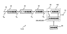
本発明の実施形態を添付の図面を参照しながら説明する。本発明の第一の実施形態は、被測定信号であるCDMA方式の信号を測定する測定装置1である。以下、図1を参照する。図1は、測定装置1の内部構成を示すブロック図である。まず、測定装置1の構成について説明する。測定装置1は、入力端子10と、前処理装置20と、アナログ・ディジタル変換装置30と、記憶装置40と、ゲートアレイ50と、制御装置60と、出力端子70とを備える。本書では、アナログ・ディジタル変換装置をA/D変換装置と略称する。
Embodiments of the present invention will be described with reference to the accompanying drawings. The first embodiment of the present invention is a measuring
入力端子10は、被測定信号SINを受信するための端子である。被測定信号SINは、CDMA方式の信号であって、疑似雑音符号(PN符号)を含む信号である。被測定信号SINの例としては、IS−95方式の信号、W−CDMA方式の信号、またはCDMA2000方式の信号などがある。前処理装置20は、入力端子10で受信する信号SINに所定の信号処理を施す装置である。前処理装置20は、例えば、被測定信号SINに含まれる測定対象外の信号を除去したり、後続する装置が被測定信号SINを処理しやすくするために被測定信号SINに周波数変換やレベル変換を施す。前処理装置20により処理された被測定信号SINは、前処理装置20から被測定信号SIFとして出力される。A/D変換装置30は、前処理装置20から出力される信号SIFを所定の時間間隔で標本化し、標本化した信号をディジタル変換し、変換結果を出力する装置である。標本化速度は、被測定信号SINのチップレートに等しい。もちろん、チップレートの2倍以上の速度でオーバーサンプリングしても良い。なお、チップは、被測定信号SINに含まれる疑似雑音符号のビットである。また、チップレートとは、被測定信号SINに含まれる疑似雑音符号が変化する速度、すなわち、ビットレートである。A/D変換装置30によりディジタル変換された信号SIFは、A/D変換装置30からデータDSとして出力される。記憶装置40は、A/D変換装置30の変換結果DSを格納するための装置である。記憶装置40は、データDSを遅滞なく格納できるアクセス能力を有する。記憶装置40には、例えば、DRAMやSRAMなどの半導体メモリが用いられる。ゲートアレイ50は、制御装置60からのデータの書き込みにより所定の処理回路が構成されるゲートアレイであって、FPGAなどのように再構成が可能なゲートアレイである。処理回路の例としては、同期捕捉装置や復調装置やBER測定装置などがある。ゲートアレイ50は、記憶装置40に格納されたデータDSを処理する。記憶装置40に格納されたデータDSは、ゲートアレイ50自身が記憶装置40から読み出しても良いし、ゲートアレイ50のために制御装置60が記憶装置40から読み出しても良い。ここで、記憶装置50は、ある一定量のデータをためてからゲートアレイ50に蓄積したデータを送るようにしてもいいし、または、A/D変換装置30の出力レートとゲートアレイ50との処理速度の差を吸収するようなバッファとして用いてもよい。一定量のデータとは、例えば、nフレーム分のデータである。一定量のデータは、拡散符号の周期が38400チップであるW−CDMAの場合、n×38400チップ分である。なお、nは、自然数である。A/D変換装置30の出力データ速度とゲートアレイ50の動作周波数が異なる場合が多いので、記憶装置40を用いることは、測定装置の設計の柔軟性向上に貢献する。制御装置60は、いわゆるコンピュータであって、プログラムを実行することにより所定の演算または処理を行う装置である。制御装置60は、上記のデータアクセスの他に、例えば、同一測定装置内の他の装置の制御を行う。なお、制御装置60は、コンピュータに相当する機能を有するデバイスであれば良いので、周辺機器やディスプレイなどを含んだコンピュータシステムに限らず、CPUやDSPなどのプロセッサ、または、コンピュータボードなどであっても良い。出力端子70は、ゲートアレイ50の処理結果が出力される端子である。
The input terminal 10 is a terminal for receiving the signal under test S IN . The signal under test S IN is a CDMA signal and includes a pseudo noise code (PN code). Examples of the signal under test S IN include an IS-95 system signal, a W-CDMA system signal, or a CDMA2000 system signal. The
ゲートアレイ50は、復調装置100と、同期捕捉装置200とを含む。復調装置100および同期捕捉装置200は、制御装置60がゲートアレイ50をプログラムすることにより、ゲートアレイ50内に構成されたものである。制御装置60によるゲートアレイ50へのプログラミングは、制御装置60によるゲートアレイ50への直接的なデータの書き込み、または、ゲートアレイ50に外部接続された図示しないメモリへの制御装置60によるデータの書き込みにより、行われる。また、制御装置60によるゲートアレイ50へのプログラミングは、制御装置60自身の動作を指示するプログラムを制御装置60が実行することにより、実施される。制御装置60自身の動作を指示するプログラムは、制御装置60内に固定的に備えられた記憶媒体、または、制御装置60に着脱可能な記憶媒体、または、制御装置60に有線接続あるいは無線接続された外部記憶媒体などに格納されている。これらの記憶媒体の例としては、制御装置60内のハードディスクドライブや半導体メモリ、または、制御装置60に着脱可能な半導体メモリデバイスやCDROMやフレキシブルディスク、または、制御装置60にUSBやネットワークなどの伝送媒体を介して接続されたハードディスクドライブやダウンロード用サーバーなどがある。さて、同期捕捉装置200は、被測定信号SINに含まれる疑似雑音符号の位相を検出する装置である。復調装置100は、同期捕捉装置200が検出した位相に基づき、被測定信号SIN(実際にはデータDS)を復調する装置である。
The
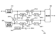
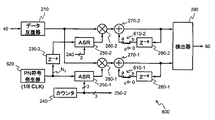
ここで、図2を参照する。図2は、同期捕捉装置200の内部構成を示すブロック図である。同期捕捉装置200は、データ反復器210と、PN符号発生器220と、遅延器230−2と、カウンタ240と、ASR250−1と、ASR250−2と、乗算器260−1と、乗算器260−2と、加算器270−1と、加算器270−2と、遅延器280−1と、遅延器280−2と、検出器290とを備える。
Reference is now made to FIG. FIG. 2 is a block diagram showing the internal configuration of the
データ反復器210は、ゲートアレイ50内に供給されているクロック信号CLKまたはクロック信号CLKを分周した信号に応じて動作し、記憶装置40から読み出されたデータDSを、クロック信号CLKの1周期TCの8倍の時間、出力し続ける装置である。なお、クロック信号CLKの速度は、被測定信号SINのチップレートよりも高く、例えば、数100MHzなどである。一般に、クロック信号CLKの最高速度は、ゲートアレイ50等のハードウェア部品の最大動作クロック周波数によって決まる。PN符号発生器220は、8TC毎に1ビットずつ疑似雑音符号N1を発生する装置である。疑似雑音符号N1は、M系列やゴールド符号など、各通信方式に必要とされる疑似雑音符号である。PN符号発生器220が発生する疑似雑音符号N1は、被測定信号SINに含まれる疑似雑音符号の1周期分の全部もしくは一部を繰り返し発生する。全相関の場合に当該1周期分の全部が発生され、部分相関の場合に当該1周期分の一部が発生される。本実施形態では、説明を簡便にするために、相関長16ビットの全相関を行うものとし、被測定信号SINに含まれる疑似雑音符号の符号長が16ビットであり、PN符号発生器220が16ビット長の疑似雑音符号を繰り返し発生するものとする。遅延器230−2、遅延器280−1、および、遅延器280−2は、入力信号または入力データに8TCの時間遅延を付加して出力する素子である。遅延器230−2、遅延器280−1、および、遅延器280−2は、例えば、シフトレジスタまたはFIFO形のメモリまたは所定長の伝送線路などである。カウンタ240は、3ビット幅の2進アップカウンタであり、0から7までの数を順に出力する。カウンタ240は、クロック信号CLKに応答してクロック信号CLKの1周期間隔で計数する。カウンタ240の計数結果は、アドレス情報として、ASR250−1およびASR250−2のそれぞれに与えられる。ASR250−1およびASR250−2のそれぞれは、アドレス可能なシフトレジスタである。なお、ASRは、Addressable Shift Registerの略称である。
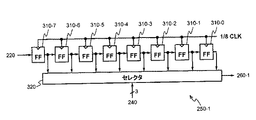
ここで、図3を参照する。図3は、ASR250−1の内部構成を示すブロック図である。ASR250−1は、8個のフリップフロップ310−0〜7と、セレクタ320とを備える。8個のフリップフロップ310−0〜7は、シフトレジスタを構成する。フリップフロップ310−7は、クロック信号CLKを8分周した信号に応答して、PN符号発生器220の出力データを取り込み、取り込んだデータを出力する。フリップフロップ310−0〜6のそれぞれは、クロック信号CLKを8分周した信号に応答して、前段のフリップフロップの出力データを取り込み、取り込んだデータを出力する。セレクタ320は、カウンタ240から3ビット幅のアドレス情報を受信する。セレクタ320は、カウンタ240からのアドレス情報に基づいて、フリップフロップ310−0〜7の出力データのいずれか1つを選択し、選択したデータを出力する。カウンタ240からのアドレス情報(アドレス値)は、選択されるフリップフロップに付された参照番号の枝番号に対応する。例えば、カウンタ240からのアドレス情報が1である時は、フリップフロップ310−1が選択される。以上のように、固定された順序およびタイミングで周期的に繰り返し疑似雑音符号が選択される。選択されたデータは、ASR250−1の出力として、乗算器260−1へ供給される。
Reference is now made to FIG. FIG. 3 is a block diagram showing the internal configuration of ASR 250-1. The ASR 250-1 includes eight flip-flops 310-0 to 7 and a
ここで、図2を参照する。ASR250−2は、ASR250−1と同一構成および同一機能を有するので、詳細な説明は省略する。乗算器260−1は、ASR250−1の出力データとデータ反復器210の出力データとを乗じ、乗算結果を出力する装置である。乗算器260−2は、ASR250−2の出力データとデータ反復器210の出力データとを乗じ、乗算結果を出力する装置である。加算器270−1は、乗算器260−1の出力データと遅延器280−1の出力データとを加算し、加算結果を出力する装置である。加算器270−2は、乗算器260−2の出力データと遅延器280−2の出力データとを加算し、加算結果を出力する装置である。加算器270−1と遅延器280−1は、累積加算器を構成している。また、加算器270−2と遅延器280−2は、累積加算器を構成している。検出器290は、加算器270−1および加算器270−2の出力データを参照して、被測定信号SINに含まれる疑似雑音符号の位相を検出する装置である。
Reference is now made to FIG. Since ASR 250-2 has the same configuration and the same function as ASR 250-1, detailed description thereof is omitted. Multiplier 260-1 is a device that multiplies the output data of ASR 250-1 and the output data of
次に、測定装置1の全体動作について説明する。ここで、図1を参照する。被測定信号SINは、前処理装置20により処理された後、A/D変換装置30によりディジタル変換され、記憶装置40に格納される。同期捕捉装置200は、記憶装置40に格納されたデータDSに基づき、被測定信号SINに含まれる疑似雑音符号の位相を検出する。最後に、復調装置100は、同期捕捉装置200が検出した位相に基づき、被測定信号SIN(実際にはデータDS)を復調する。
Next, the overall operation of the measuring
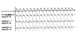
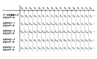
次に、同期捕捉装置200の動作について説明する。ここで、図2と図4を参照する。図4は、データ反復器210の出力データおよびASR250−1の出力データおよびASR250−2の出力データを示すタイミングチャートである。図4において、横軸は時間である。また、図4における縦破線は、クロック信号CLKの周期間隔で並んでいる。下付数字を有するアルファベット記号「S」は、タイムスロットを表している。タイムスロットの時間間隔は、TCである。下付数字を有するアルファベット記号「X」は、データ反復器210の出力データを表している。データ反復器210の出力データは、8TC毎に新たなビットデータが出力される。下付数字を有するアルファベット記号「C」は、疑似雑音符号N1の各ビットデータを示している。アルファベット記号「C」の下付数字は、PN符号発生器220から出力されるビットデータの順番を表している。すなわち、C0、C1,C2・・・の順に出力される。なお、疑似雑音符号N1は繰り返し発生されるので、C15の次はC0が出力される。さて、ASR260−1およびASR260−2は、位相が異なる8種類の疑似雑音符号を時分割多重して出力する。ASR260−1から出力される8種の疑似雑音符号は、ASR260−2から出力される8種の疑似雑音符号と位相が異なる。言うまでもないが、この場合の位相とは、疑似雑音符号N1の位相である。乗算器260−1および乗算器260−2では、順次、乗算処理が行われる。そして、加算器270−1は、乗算器260−1の乗算結果に、8TC前の加算器270−1の出力データを加算して、加算結果を出力する。すなわち、加算器270−1は、タイムスロットごとに、乗算器260−1の乗算結果を累積加算する。一方、加算器270−2は、乗算器260−2の乗算結果に、8TC前の加算器270−2の出力データを加算して、加算結果を出力する。すなわち、加算器270−2は、タイムスロットごとに、乗算器260−2の乗算結果を累積加算する。
Next, the operation of the
上記の演算を開始してから一定時間経過後、疑似雑音符号N1の全16ビットについての乗算結果の累積加算結果が、疑似雑音符号N1の位相ごとに、加算器270−1および加算器270−2のそれぞれから出力される。例えば、加算器270−1から、X0・C0+X1・C1+X2・C2+X3・C3+X4・C4+X5・C5+X6・C6+X7・C7+X8・C8+X9・C9+X10・C10+X11・C11+X12・C12+X13・C13+X14・C14+X15・C15の結果Y0が出力される。なお、Y0は、疑似雑音符号N1の先頭チップの位相を最初の入力データX0と一致させた時の演算結果である。また、疑似雑音符号N1の先頭チップの位相を最初の入力データX0に対してnチップ分シフトした時の乗算結果の累積加算結果をYnとする。さて、演算結果Y0の出力開始から9TC後、X1・C0+X2・C1+X3・C2+X4・C3+X5・C4+X6・C5+X7・C6+X8・C7+X9・C8+X10・C9+X11・C10+X12・C11+X13・C12+X14・C13+X15・C14+X16・C15の結果、すなわち、演算結果Y1が出力される。このように演算結果Y1〜Y7が、9TC毎に順次、加算器270−1から出力される。演算結果Y7が出力された後に続けて、加算器270−2からは、X8・C0+X9・C1+X10・C2+X11・C3+X12・C4+X13・C5+X14・C6+X15・C7+X16・C8+X17・C9+X18・C10+X19・C11+X20・C12+X21・C13+X22・C14+X23・C15の結果Y8が出力される。上記と同様に、演算結果Y8〜Y15が、9TC毎に順次、加算器270−2から出力される。ちなみに、Y15=X15・C0+X16・C1+X17・C2+X18・C3+X19・C4+X20・C5+X21・C6+X22・C7+X23・C8+X24・C9+X25・C10+X26・C11+X27・C12+X28・C13+X29・C14+X30・C15、である。 After a predetermined time has elapsed from the start of the calculation of the multiplication result of the cumulative addition results for all 16 bits of the pseudo-noise code N 1 is, for each phase of the pseudo-noise code N 1, adders 270-1 and an adder 270-2. For example, from the adder 270-1, X 0 · C 0 + X 1 · C 1 + X 2 · C 2 + X 3 · C 3 + X 4 · C 4 + X 5 · C 5 + X 6 · C 6 + X 7 · C 7 + X The result Y 0 of 8 · C 8 + X 9 · C 9 + X 10 · C 10 + X 11 · C 11 + X 12 · C 12 + X 13 · C 13 + X 14 · C 14 + X 15 · C 15 is output. Y 0 is a calculation result when the phase of the head chip of the pseudo noise code N 1 is matched with the first input data X 0 . Further, the cumulative addition result of the multiplication results when the phase of the first chip of the pseudo noise code N 1 is shifted by n chips with respect to the first input data X 0 is Y n . Now, 9 T C after the start of the output of the operation result Y 0 , X 1 · C 0 + X 2 · C 1 + X 3 · C 2 + X 4 · C 3 + X 5 · C 4 + X 6 · C 5 + X 7 · C 6 + X 8・ C 7 + X 9・ C 8 + X 10・ C 9 + X 11・ C 10 + X 12・ C 11 + X 13・ C 12 + X 14・ C 13 + X 15・ C 14 + X 16・ C 15 The result Y 1 is output. As described above, the calculation results Y 1 to Y 7 are sequentially output from the adder 270-1 every 9 T C. After the calculation result Y 7 is output, the adder 270-2 outputs X 8 · C 0 + X 9 · C 1 + X 10 · C 2 + X 11 · C 3 + X 12 · C 4 + X 13 · C 5 + X 14 · C 6 + X 15 · C 7 + X 16 · C 8 + X 17 · C 9 + X 18 · C 10 + X 19 · C 11 + X 20 · C 12 + X 21 · C 13 + X 22 · C 14 + X 23 · C 15 As a result, Y 8 is output. Similarly to the above, the calculation results Y 8 to Y 15 are sequentially output from the adder 270-2 every 9T C. By the way, Y 15 = X 15 · C 0 + X 16 · C 1 + X 17 · C 2 + X 18 · C 3 + X 19 · C 4 + X 20 · C 5 + X 21 · C 6 + X 22 · C 7 + X 23 · C 8 + X 24 · C 9 + X 25 · C 10 + X 26 · C 11 + X 27 · C 12 + X 28 · C 13 + X 29 · C 14 + X 30 · C 15
疑似雑音符号N1の全16ビットについての乗算結果を累積加算した結果は、被測定信号SIN(実際にはデータDS)と疑似雑音符号N1との相関値として利用することができる。そして最終的には、疑似雑音符号N1の位相ごとの相関値として、全部で16個の累積加算結果Y0〜Y15が得られる。本実施形態では、関連する疑似雑音符号N1の位相がそれぞれ異なる16種類の相関演算を、並列化しかつ時間的に多重化して処理している(並列度2、時分割多重度8)。ここで、本方式を従来のスライディング相関器と比較してみると、回路規模は並列化により2倍になるが、処理速度はクロック信号CLKが入力データレートと同じであると仮定した場合1/2に短縮されている。また、本方式を従来のマッチトフィルタと比較してみると、回路規模は多重化により1/8になり、処理速度はクロック信号CLKが入力データレートと同じであると仮定した場合8倍になる。なお、本実施形態のように、クロック信号CLKを入力データレートよりも高速にすれば、従来の方法より同等あるいはそれ以上に高速に上記処理を行うことができる。
As a result of cumulative addition of the multiplication results for all 16 bits of the pseudo-noise code N 1 it can be used as a correlation value between the measured signal S IN (actually data D S) and the pseudo-noise code N 1. Finally, as a correlation value for each phase of the pseudo noise code N 1 , a total of 16 cumulative addition results Y 0 to Y 15 are obtained. In the present embodiment, 16 types of correlation operations having different phases of the related pseudo-noise code N 1 are processed in parallel and temporally multiplexed (
検出器290は、加算器270−1および加算器270−2から出力される上記16個の累積加算結果のうち絶対値が最大のものを検出する。検出された累積加算結果に関連する疑似雑音符号N1の位相が、復調装置100へ出力される。そして、復調装置100は、同期捕捉装置200が出力した位相情報に基づき、被測定信号SIN(実際にはデータDS)を復調する。
次に、本発明の第二の実施形態について説明する。本発明の第二の実施形態は、被測定信号であるCDMA方式の信号を測定する測定装置2である。ここで、図1を参照する。測定装置2は、測定装置1において同期捕捉装置200が同期捕捉装置400に置き換わったものである。すなわち、構成要素の点から見れば、測定装置1と測定装置2とに相違はない。制御装置60によりゲートアレイ50内で実現される装置が異なるのみである。従って、測定装置2の構成要素のうち、測定装置1と共通する要素については、説明を省略する。
Next, a second embodiment of the present invention will be described. The second embodiment of the present invention is a measuring
同期捕捉装置400は、制御装置60がゲートアレイ50をプログラムすることにより、ゲートアレイ50内に構成されたものである。同期捕捉装置400は、被測定信号SINに含まれる疑似雑音符号の位相を検出する装置である。復調装置100は、同期捕捉装置400が検出した位相に基づき、被測定信号SIN(実際にはデータDS)を復調する装置である。
The
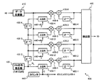
ここで、図5を参照する。図5は、同期捕捉装置400の内部構成を示すブロック図である。同期捕捉装置400は、データ反復器410と、PN符号発生器420と、遅延器430−2と、遅延器430−3と、遅延器430−4と、カウンタ440と、ASR450−1と、ASR450−2と、ASR450−3と、ASR450−4と、乗算器460−1と、乗算器460−2と、乗算器460−3と、乗算器460−4と、加算器470−1と、加算器470−2と、加算器470−3と、加算器470−4と、遅延器480−1と、遅延器480−2と、遅延器480−3と、遅延器480−4と、検出器490とを備える。
Reference is now made to FIG. FIG. 5 is a block diagram showing an internal configuration of the
データ反復器410は、ゲートアレイ50内に供給されているクロック信号CLKまたはクロック信号CLKを分周した信号に応じて動作し、記憶装置40から読み出されたデータDSを、クロック信号CLKの1周期TCの4倍の時間、出力し続ける装置である。なお、クロック信号CLKの速度は、被測定信号SINのチップレートよりも高く、例えば、数100MHzなどである。一般に、クロック信号CLKの最高速度は、ゲートアレイ50などのハードウェア部品の最大動作クロック周波数によって決まる。PN符号発生器420は、4TC毎に1ビットずつ疑似雑音符号N2を発生する装置である。疑似雑音符号N2は、M系列やゴールド符号など、各通信方式に必要とされる疑似雑音符号である。PN符号発生器420が発生する疑似雑音符号N2は、被測定信号SINに含まれる疑似雑音符号の1周期分の全部もしくは一部を繰り返し発生する。全相関の場合に当該1周期分の全部が発生され、部分相関の場合に当該1周期分の一部が発生される。本実施形態では、説明を簡便にするために、相関長16ビットの全相関を行うものとし、被測定信号SINに含まれる疑似雑音符号の符号長が16ビットであり、PN符号発生器420が16ビット長の疑似雑音符号を繰り返し発生するものとする。遅延器430−2〜4および遅延器480−1〜4は、入力信号または入力データに4TCの時間遅延を付加して出力する素子である。遅延器430−2〜4および遅延器480−1〜4は、例えば、シフトレジスタまたはFIFO形のメモリまたは所定長の伝送線路などである。カウンタ440は、2ビット幅の2進アップカウンタであり、0から3までの数を順に出力する。カウンタ440は、クロック信号CLKに応答してクロック信号CLKの1周期間隔で計数する。カウンタ440の計数結果は、アドレス情報として、ASR450−1〜4のそれぞれに与えられる。ASR450−1〜4は、アドレス可能なシフトレジスタである。
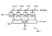
ここで、図6を参照する。図6は、ASR450−1の内部構成を示すブロック図である。ASR450−1は、4個のフリップフロップ510−0〜3と、セレクタ520とを備える。4個のフリップフロップ510−0〜3は、シフトレジスタを構成する。フリップフロップ510−3は、クロック信号CLKを4分周した信号に応答して、PN符号発生器420の出力データを取り込み、取り込んだデータを出力する。フリップフロップ510−0〜2のそれぞれは、クロック信号CLKを4分周した信号に応答して、前段のフリップフロップの出力データを取り込み、取り込んだデータを出力する。セレクタ520は、カウンタ440から2ビット幅のアドレス情報を受信する。セレクタ520は、カウンタ440からのアドレス情報に基づいて、フリップフロップ510−0〜3の出力データのいずれか1つを選択し、選択したデータを出力する。選択されたデータは、ASR450−1の出力として、乗算器460−1へ供給される。なお、カウンタ440からのアドレス情報(アドレス値)は、選択されるフリップフロップに付された参照番号の枝番号に対応する。例えば、カウンタ440からのアドレス情報が1である時は、フリップフロップ510−1が選択される。
Reference is now made to FIG. FIG. 6 is a block diagram showing an internal configuration of ASR 450-1. The ASR 450-1 includes four flip-flops 510-0 to 510-3 and a
ここで、図5を参照する。ASR450−2〜4のそれぞれは、ASR450−1と同一構成および同一機能を有するので、詳細な説明は省略する。乗算器460−1は、ASR450−1の出力データとデータ反復器410の出力データとを乗じ、乗算結果を出力する装置である。乗算器460−2は、ASR450−2の出力データとデータ反復器410の出力データとを乗じ、乗算結果を出力する装置である。乗算器460−3は、ASR450−3の出力データとデータ反復器410の出力データとを乗じ、乗算結果を出力する装置である。乗算器460−4は、ASR450−4の出力データとデータ反復器410の出力データとを乗じ、乗算結果を出力する装置である。加算器470−1は、乗算器460−1の出力データと遅延器480−1の出力データとを加算し、加算結果を出力する装置である。加算器470−2は、乗算器460−2の出力データと遅延器480−2の出力データとを加算し、加算結果を出力する装置である。加算器470−3は、乗算器460−3の出力データと遅延器480−3の出力データとを加算し、加算結果を出力する装置である。加算器470−4は、乗算器460−4の出力データと遅延器480−4の出力データとを加算し、加算結果を出力する装置である。加算器470−1と遅延器480−1は、累積加算器を構成している。また、加算器470−2と遅延器480−2は、累積加算器を構成している。加算器470−3と遅延器480−3は、累積加算器を構成している。加算器470−4と遅延器480−4は、累積加算器を構成している。検出器490は、加算器470−1〜4のそれぞれの出力データを参照して、被測定信号SINに含まれる疑似雑音符号の位相を検出する装置である。
Reference is now made to FIG. Since each of ASR 450-2 to 4 has the same configuration and the same function as ASR 450-1, detailed description thereof is omitted. Multiplier 460-1 is a device that multiplies the output data of ASR 450-1 and the output data of
次に、測定装置2の全体動作について説明する。ここで、図1を参照する。被測定信号SINは、前処理装置20により処理された後、A/D変換装置30によりディジタル変換され、記憶装置40に格納される。同期捕捉装置400は、記憶装置40に格納されたデータDSに基づき、被測定信号SINの疑似雑音符号の位相を検出する。最後に、復調装置100は、同期捕捉装置400が検出した位相に基づき、被測定信号SIN(実際にはデータDS)を復調する。
Next, the overall operation of the measuring
次に、同期捕捉装置400の動作について説明する。ここで、図5と図7を参照する。図7は、データ反復器410の出力データおよびASR450−1〜4のそれぞれの出力データを示すタイミングチャートである。図7において、横軸は時間である。また、図7における縦破線は、クロック信号CLKの周期間隔で並んでいる。下付数字を有するアルファベット記号「S」は、タイムスロットを表している。タイムスロットの時間間隔は、TCである。下付数字を有するアルファベット記号「X」は、データ反復器410の出力データを表している。データ反復器410の出力データは、4TC毎に新たなビットデータが出力される。下付数字を有するアルファベット記号「C」は、疑似雑音符号N2の各ビットデータを示している。アルファベット記号「C」の下付数字は、PN符号発生器420から出力されるビットデータの順番を表している。すなわち、C0、C1,C2・・・の順に出力される。なお、疑似雑音符号N2は繰り返し発生されるので、C15の次はC0が出力される。さて、ASR460−1〜4のそれぞれは、位相が異なる4種類の疑似雑音符号を時分割多重して出力する。あるASRから出力される4種の疑似雑音符号は、他の3つのASRから出力される4種の疑似雑音符号と位相が異なる。この場合の位相とは、疑似雑音符号N2の位相である。乗算器460−1〜4のそれぞれにおいて、順次、乗算処理が行われる。そして、加算器470−1は、乗算器460−1の乗算結果に、4TC前の加算器470−1の出力データを加算して、加算結果を出力する。すなわち、加算器470−1は、タイムスロットごとに、乗算器460−1の乗算結果を累積加算する。加算器470−2は、乗算器460−2の乗算結果に、4TC前の加算器470−2の出力データを加算して、加算結果を出力する。すなわち、加算器470−2は、タイムスロットごとに、乗算器460−2の乗算結果を累積加算する。加算器470−3は、乗算器460−3の乗算結果に、4TC前の加算器470−3の出力データを加算して、加算結果を出力する。すなわち、加算器470−3は、タイムスロットごとに、乗算器460−3の乗算結果を累積加算する。加算器470−4は、乗算器460−4の乗算結果に、4TC前の加算器470−4の出力データを加算して、加算結果を出力する。すなわち、加算器470−4は、タイムスロットごとに、乗算器460−4の乗算結果を累積加算する。
Next, the operation of the
上記の演算を開始してから一定時間経過後、疑似雑音符号N2の全16ビットについての乗算結果の累積加算結果が、疑似雑音符号N2の位相ごとに、加算器470−1〜4のそれぞれから順次出力される。例えば、加算器470−1から、X0・C0+X1・C1+X2・C2+X3・C3+X4・C4+X5・C5+X6・C6+X7・C7+X8・C8+X9・C9+X10・C10+X11・C11+X12・C12+X13・C13+X14・C14+X15・C15の結果Y0が出力される。なお、Y0は、疑似雑音符号N1の先頭チップの位相を最初の入力データX0と一致させた時の演算結果である。また、疑似雑音符号N1の先頭チップの位相を最初の入力データX0に対してnチップ分シフトした時の乗算結果の累積加算結果をYnとする。さて、演算結果Y0の出力開始から5TC後に、X1・C0+X2・C1+X3・C2+X4・C3+X5・C4+X6・C5+X7・C6+X8・C7+X9・C8+X10・C9+X11・C10+X12・C11+X13・C12+X14・C13+X15・C14+X16・C15の結果、すなわち、演算結果Y1が出力される。演算結果Y0〜Y3は、5TC毎に順次、加算器470−1から出力される。Y3が出力された後に続けて、加算器470−2からは、X4・C0+X5・C1+X6・C2+X7・C3+X8・C4+X9・C5+X10・C6+X11・C7+X12・C8+X13・C9+X14・C10+X15・C11+X16・C12+X17・C13+X18・C14+X19・C15の結果Y4が出力される。上記同様に、演算結果Y4〜Y7は、5TC毎に順次、加算器470−2から出力される。Y7が出力された後に続けて、加算器470−3からは、5TC毎に、演算結果Y8〜Y11が順次出力される。Y11が出力された後に続けて、加算器470−4からは、5TC毎に演算結果Y12〜Y15が順次出力される。 After a predetermined time has elapsed from the start of the calculation of the cumulative addition result of the multiplication results for all 16 bits of the pseudo-noise code N 2 is the pseudo-noise code N 2 for each phase, the adder 470-1~4 Output sequentially from each. For example, from the adder 470-1, X 0 · C 0 + X 1 · C 1 + X 2 · C 2 + X 3 · C 3 + X 4 · C 4 + X 5 · C 5 + X 6 · C 6 + X 7 · C 7 + X The result Y 0 of 8 · C 8 + X 9 · C 9 + X 10 · C 10 + X 11 · C 11 + X 12 · C 12 + X 13 · C 13 + X 14 · C 14 + X 15 · C 15 is output. Y 0 is a calculation result when the phase of the head chip of the pseudo noise code N 1 is matched with the first input data X 0 . Further, the cumulative addition result of the multiplication results when the phase of the first chip of the pseudo noise code N 1 is shifted by n chips with respect to the first input data X 0 is Y n . Now, 5 T C after the start of the output of the operation result Y 0 , X 1 · C 0 + X 2 · C 1 + X 3 · C 2 + X 4 · C 3 + X 5 · C 4 + X 6 · C 5 + X 7 · C 6 + X 8・ C 7 + X 9・ C 8 + X 10・ C 9 + X 11・ C 10 + X 12・ C 11 + X 13・ C 12 + X 14・ C 13 + X 15・ C 14 + X 16・ C 15 The result Y 1 is output. Operation results Y 0 to Y 3 sequentially every 5T C, output from the adder 470-1. After the output of Y 3 , the adder 470-2 outputs X 4 · C 0 + X 5 · C 1 + X 6 · C 2 + X 7 · C 3 + X 8 · C 4 + X 9 · C 5 + X 10・ C 6 + X 11・ C 7 + X 12・ C 8 + X 13・ C 9 + X 14・ C 10 + X 15・ C 11 + X 16・ C 12 + X 17・ C 13 + X 18・ C 14 + X 19・ C 15 Y 4 is output. In the same manner as described above, the operation result Y 4 to Y 7 sequentially for each 5T C, output from the adder 470-2. After the output of Y 7 , the calculation results Y 8 to Y 11 are sequentially output from the adder 470-3 every 5T C. After the output of Y 11 , operation results Y 12 to Y 15 are sequentially output from the adder 470-4 every 5 T C.
疑似雑音符号N2の全16ビットについての乗算結果を累積加算した結果は、被測定信号SIN(実際にはデータDS)と疑似雑音符号N2との相関値として利用することができる。そして最終的には、疑似雑音符号N1の位相ごとの相関値として、全部で16個の累積加算結果Y0〜Y15が得られる。本実施形態では、関連する疑似雑音符号N1の位相がそれぞれ異なる16種類の相関演算を、並列化しかつ時間的に多重化して処理している(並列度4、時分割多重度4)。ここで、本方式を従来のスライディング相関器と比較してみると、回路規模は並列化により4倍になるが、処理速度はクロック信号CLKが入力データレートと同じであると仮定した場合1/4に短縮されている。また、本方式を従来のマッチトフィルタと比較してみると、回路規模は多重化により1/4になり、処理速度はクロック信号CLKが入力データレートと同じであると仮定した場合4倍になる。なお、本実施形態のように、クロック信号CLKを入力データレートよりも高速にすれば、従来の方法より同等あるいはそれ以上に高速に上記処理を行うことができる。
As a result of cumulative addition of the multiplication results for all 16 bits of the pseudo-noise code N 2 can be used as a correlation value between the measured signal S IN (actually data D S) and the pseudo-noise code N 2. Finally, as a correlation value for each phase of the pseudo noise code N 1 , a total of 16 cumulative addition results Y 0 to Y 15 are obtained. In the present embodiment, 16 types of correlation operations having different phases of the related pseudo-noise code N 1 are processed in parallel and temporally multiplexed (
検出器490は、加算器470−1〜4のそれぞれから出力される上記16個の累積加算結果のうち絶対値が最大のものを検出する。検出された累積加算結果に関連する疑似雑音符号N2の位相が、復調装置100へ出力される。そして、復調装置100は、同期捕捉装置400が出力した位相情報に基づき、被測定信号SINを復調する。
The
ところで、上記の各実施形態は、いずれも全相関が採用されている。本発明は、同期捕捉のために、全相関のみならず部分相関も採用しうる。そこで、部分相関による同期捕捉を行う、本発明の第三の実施形態について以下に説明する。 By the way, in each of the above embodiments, all correlations are adopted. The present invention can employ not only full correlation but also partial correlation for synchronization acquisition. Therefore, a third embodiment of the present invention that performs synchronization acquisition by partial correlation will be described below.
本発明の第三の実施形態は、被測定信号であるCDMA方式の信号を測定する測定装置3である。ここで、図1を参照する。測定装置3は、測定装置1において同期捕捉装置200が同期捕捉装置600に置き換わったものである。すなわち、構成要素の点から見れば、測定装置1と測定装置2とに相違はない。制御装置60によりゲートアレイ50内で実現される装置が異なるのみである。従って、測定装置3の構成要素のうち、測定装置1と共通する要素については、説明を省略する。
The third embodiment of the present invention is a measuring
同期捕捉装置600は、制御装置60がゲートアレイ50をプログラムすることにより、ゲートアレイ50内に構成されたものである。同期捕捉装置600は、被測定信号SINに含まれる疑似雑音符号の位相を検出する装置である。復調装置100は、同期捕捉装置600が検出した位相に基づき、被測定信号SIN(実際にはデータDS)を復調する装置である。
The
ここで、図8を参照する。図8は、同期捕捉装置600の内部構成を示すブロック図である。同期捕捉装置600は、同期捕捉装置200の構成要素に加えて、加算器270−1と遅延器280−1との間にスイッチ610−1を、加算器270−2と遅延器280−2との間にスイッチ610−2を備える。スイッチ610−1およびスイッチ610−2は、単極双投形(SPDT形)のスイッチである。また、同期捕捉装置600は、PN符号発生器220の代わりにPN符号発生器620を備える。さらに、図8において、図2と同じ構成要素については、同一の参照符号を付して詳細な説明を省略する。
Reference is now made to FIG. FIG. 8 is a block diagram showing the internal configuration of the
スイッチ610−1およびスイッチ610−2において、端子aが共通端子である。スイッチ610−1の端子aは、加算器270−1に接続されている。スイッチ610−1の端子bは、遅延器280−1に接続され、遅延器280−1の出力データが供給される。スイッチ610−1の端子cは、ゼロが供給されている。スイッチ610−2の端子aは、加算器270−2に接続されている。スイッチ610−2の端子bは、遅延器280−2に接続され、遅延器280−2の出力データが供給される。スイッチ610−1の端子cは、ゼロが供給されている。加算器270−1は、乗算器260−1の出力データとスイッチ610−1の端子aに現れるデータとを加算し、加算結果を出力する。加算器270−2は、乗算器260−2の出力データとスイッチ610−2の端子aに現れるデータとを加算し、加算結果を出力する。 In the switches 610-1 and 610-2, the terminal a is a common terminal. The terminal a of the switch 610-1 is connected to the adder 270-1. The terminal b of the switch 610-1 is connected to the delay device 280-1, and the output data of the delay device 280-1 is supplied. Zero is supplied to the terminal c of the switch 610-1. The terminal a of the switch 610-2 is connected to the adder 270-2. The terminal b of the switch 610-2 is connected to the delay device 280-2, and the output data of the delay device 280-2 is supplied. Zero is supplied to the terminal c of the switch 610-1. Adder 270-1 adds the output data of multiplier 260-1 and the data appearing at terminal a of switch 610-1, and outputs the addition result. Adder 270-2 adds the output data of multiplier 260-2 and the data appearing at terminal a of switch 610-2, and outputs the addition result.
PN符号発生器620は、8TC毎に1ビットずつ疑似雑音符号N3を発生する装置である。疑似雑音符号N3は、M系列やゴールド符号など、各通信方式に必要とされる疑似雑音符号である。ただし、この疑似雑音符号N3は、ある疑似雑音符号の一部分である。本実施形態において、PN符号発生器620が発生する疑似雑音符号N3は、拡散符号の周期が38400チップであるW−CDMAを例にとり、符号長38400ビットの疑似雑音符号の先頭から16ビット分の符号とする。疑似雑音符号N3は、PN符号発生器620により繰り返し発生される。疑似雑音符号N3は、ASR250−1に、および、遅延器230−2を介してASR250−2に供給される。
The
次に、測定装置3の全体動作について説明する。ここで、図1を参照する。被測定信号SINは、前処理装置20により処理された後、A/D変換装置30によりディジタル変換され、記憶装置40に格納される。同期捕捉装置600は、記憶装置40に格納されたデータDSに基づき、被測定信号SINに含まれる疑似雑音符号の位相を検出する。最後に、復調装置100は、同期捕捉装置600が検出した位相に基づき、被測定信号SIN(実際にはデータDS)を復調する。
Next, the overall operation of the measuring
次に、同期捕捉装置600の動作について説明する。ここで、図8と図9を参照する。図9は、データ反復器210の出力データおよびASR250−1〜4のそれぞれの出力データを示すタイミングチャートである。図9において、横軸は時間である。また、図9における縦破線は、クロック信号CLKの周期間隔で並んでいる。図9の下図は、図9の上図に時間的に後続するチャートである。下付数字を有するアルファベット記号「S」は、タイムスロットを表している。タイムスロットの時間間隔は、TCである。下付数字を有するアルファベット記号「X」は、データ反復器210の出力データを表している。データ反復器210の出力データは、8TC毎に新たなビットデータが出力される。下付数字を有するアルファベット記号「C」は、疑似雑音符号N3の各ビットデータを示している。アルファベット記号「C」の下付数字は、PN符号発生器220から出力されるビットデータの順番を表している。すなわち、C0、C1,C2・・・の順に出力される。なお、疑似雑音符号N3は繰り返し発生されるので、C15の次はC0が出力される。また、疑似雑音符号N3が疑似雑音符号の一部であるので、C0との乗算結果から順に累積加算することを要し、C0が現れるまでのビットデータおよび当該ビットデータに関連する演算は全て無効となる。そのような無効なビットデータは、タイミングチャート(図9)において記号「−」として表示されている。
Next, the operation of the
さて、乗算器260−1〜2のそれぞれ、および、加算器270−1〜2のそれぞれは、継続的に演算を繰り返している。スイッチ610−1およびスイッチ610−2は、無効なビットデータに係る乗算結果が累積加算処理に反映されないように選択動作を行う。すなわち、スイッチ610−1は、加算器270−1に入力されるデータ(乗算結果)に関連するASR250−1の出力データがC0である時、端子cを選択する。これにより、加算器270−1に係る累積加算値が初期化される。一方、スイッチ610−1は、加算器270−1に入力されるデータ(乗算結果)に関連するASR250−1の出力データがC0以外である時、端子bを選択する。また、スイッチ610−2は、加算器270−2に入力されるデータ(乗算結果)に関連するASR250−2の出力データがC0である時、端子cを選択する。これにより、加算器270−2に係る累積加算値が初期化される。一方、スイッチ610−2は、加算器270−2に入力されるデータ(乗算結果)に関連するASR250−2の出力データがC0以外である時、端子bを選択する。より具体的な例を挙げると、データ反復器210の出力データがX0である時のタイムスロットS0、および、データ反復器210の出力データがX1である時のタイムスロットS1においてスイッチ610−1の端子cが選択され、加算器270−1にゼロが供給される。そして、データ反復器210の出力データがX1である時のタイムスロットS0、および、データ反復器210の出力データがX2である時のタイムスロットS1において、スイッチ610−1の端子bが選択され、加算器270−1に遅延器280−1の出力データが供給される。また、例えば、データ反復器210の出力データがX8である時のタイムスロットS0、および、データ反復器210の出力データがX9である時のタイムスロットS1において、スイッチ610−2の端子cが選択され、加算器270−2にゼロが供給される。そして、データ反復器210の出力データがX9である時のタイムスロットS0、および、データ反復器210の出力データがX10である時のタイムスロットS1において、スイッチ610−2の端子bが選択され、加算器270−2に遅延器280−2の出力データが供給される。 Now, each of the multipliers 260-1 and 260-2 and the adders 270-1 and 270-2 are continuously repeated. The switches 610-1 and 610-2 perform a selection operation so that the multiplication result related to invalid bit data is not reflected in the cumulative addition process. That is, the switch 610-1, when the output data of ASR250-1 associated with data input to the adder 270-1 (multiplication results) are C 0, selects the terminal c. As a result, the cumulative addition value related to the adder 270-1 is initialized. On the other hand, the switch 610-1, when the output data of ASR250-1 associated with data input to the adder 270-1 (multiplication results) is other than C 0, selects the terminal b. The switch 610-2, when the output data of ASR250-2 associated with data input to the adder 270-2 (multiplication results) are C 0, selects the terminal c. As a result, the cumulative addition value related to the adder 270-2 is initialized. On the other hand, the switch 610-2, when the output data of ASR250-2 associated with data input to the adder 270-2 (multiplication results) is other than C 0, selects the terminal b. As a more specific example, the switch is performed in the time slot S 0 when the output data of the data repeater 210 is X 0 and in the time slot S 1 when the output data of the data repeater 210 is X 1. The terminal c of 610-1 is selected, and zero is supplied to the adder 270-1. In the time slot S 0 when the output data of the data repeater 210 is X 1 and the time slot S 1 when the output data of the data repeater 210 is X 2 , the terminal b of the switch 610-1 And the output data of the delay unit 280-1 is supplied to the adder 270-1. Further, for example, in the time slot S 0 when the output data of the data repeater 210 is X 8 and in the time slot S 1 when the output data of the data repeater 210 is X 9 , the switch 610-2 The terminal c is selected and zero is supplied to the adder 270-2. Then, in the time slot S 0 when the output data of the data repeater 210 is X 9 and the time slot S 1 when the output data of the data repeater 210 is X 10 , the terminal b of the switch 610-2 And the output data of the delay unit 280-2 is supplied to the adder 270-2.
第一の実施形態と同様に、リセットから一定時間経過すると、疑似雑音符号N3の全16ビットについての乗算結果の累積加算結果が、疑似雑音符号N3の位相ごとに、加算器270−1および加算器270−2のそれぞれから順次出力される。ここで、疑似雑音符号N3の先頭チップの位相を最初の入力データX0に対してnチップ分シフトした時の乗算結果の累積加算結果をYnとする。各累積加算結果が出力されるタイミングは、第一の実施形態と同様に、加算器270−1から9TC毎に順次、演算結果Y0〜Y7が出力される。Y7が出力された後に続いて、加算器270−2から9TC毎に順次、Y8〜Y15が出力される。 Like the first embodiment, when a predetermined time has elapsed from the reset, the cumulative addition result of the multiplication results for all 16 bits of the pseudo-noise code N 3 is, for each phase of the pseudo-noise code N 3, adders 270-1 And the adder 270-2 sequentially output. Here, the cumulative addition result of the multiplication results when the phase of the head chip of the pseudo noise code N 3 is shifted by n chips with respect to the first input data X 0 is Y n . As for the timing at which each cumulative addition result is output, the calculation results Y 0 to Y 7 are sequentially output from the adders 270-1 to 9 T C as in the first embodiment. Following after Y 7 is outputted sequentially from the adder 270-2 per 9T C, Y 8 ~Y 15 is output.
前述の通り、スイッチ610−1は、加算器280−1に入力されるデータ(乗算結果)に関連するASR250−1の出力データがC0である時、端子cを選択する。また、スイッチ610−2は、加算器280−1に入力されるデータ(乗算結果)に関連するASR250−1の出力データがC0である時、端子cを選択する。これらの動作により、随時、累積加算値が初期化されていく。従って、演算結果Y0〜Y15のそれぞれが出力された後、演算結果Y0〜Y15のそれぞれに関連する累積加算値が初期化され、新たに累積加算が開始される。そして、加算器270−1から9TC毎に順次、演算結果Y16〜Y23が出力される。Y23が出力された後に続いて、加算器270−2から9TC毎に順次、Y24〜Y31が出力される。新たな累積加算を1つ開始すると、1チップ分だけサーチ区間が広がる。このようにしてサーチ区間を広げることにより、例えば、W−CDMAで信号拡散に用いられる疑似雑音符号の全長38400チップの区間における部分相関処理を実施することができる。 As described above, the switch 610-1, when the output data of ASR250-1 associated with data input to the adder 280-1 (multiplication results) are C 0, selects the terminal c. The switch 610-2, when the output data of ASR250-1 associated with data input to the adder 280-1 (multiplication results) are C 0, selects the terminal c. With these operations, the accumulated addition value is initialized at any time. Thus, after the respective operation results Y 0 to Y 15 is output, the accumulated value associated with each of the calculation results Y 0 to Y 15 are initialized, a new cumulative addition is started. Then, the calculation results Y 16 to Y 23 are sequentially output from the adder 270-1 every 9 T C. Following after Y 23 is outputted sequentially from the adder 270-2 per 9T C, Y 24 ~Y 31 is output. When one new cumulative addition is started, the search interval is expanded by one chip. By expanding the search interval in this way, for example, partial correlation processing can be performed in the interval of the total length of 38400 chips of the pseudo-noise code used for signal spreading in W-CDMA.
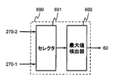
さて、各累積加算結果は異なる時間に出力されるので、検出器290を図10に示される検出器690に置き換えることができる。ここで、図10を参照する。図10は、検出器690の内部構成の一例を示す図である。検出器690は、加算器270−1の出力データと加算器270−2の出力データのいずれかを選択して出力するセレクタ691と、セレクタ691の出力データから絶対値が最大のものを検出し、当該最大値に対応する疑似雑音符号N3の位相を出力する最大値検出器692を備える。このような検出器690は、加算器に対応して2つの最大値検出器を備える必要がない分だけ構成が簡易であり、ゲートアレイ・リソースの消費が少ない。
Now, since each cumulative addition result is output at a different time, the
また、本第三の実施形態において、累積加算値を初期化する手段はスイッチに限定されない。加算器に供給される乗算結果に対応する疑似雑音符号のデータが当該疑似雑音符号の先頭データである時に、当該乗算結果とともに加算器に入力されるデータをゼロにする手段であれば何でも良い。例えば、加算器に接続される遅延器が、対応するASRに内蔵されるものと同じ段数のシフトレジスタで構成される場合、乗算器に供給される疑似雑音符号に基づいてシフトレジスタの所定のフリップフロップを適当な時期にリセットするような制御装置をスイッチの代わりに利用できる。 In the third embodiment, the means for initializing the cumulative added value is not limited to the switch. Any means may be used as long as the data input to the adder together with the multiplication result is zero when the pseudo noise code data corresponding to the multiplication result supplied to the adder is the head data of the pseudo noise code. For example, when the delay device connected to the adder is configured with a shift register having the same number of stages as that incorporated in the corresponding ASR, the predetermined flip-flop of the shift register is based on the pseudo-noise code supplied to the multiplier. A control device can be used in place of the switch to reset the device at an appropriate time.
なお、第二の実施形態の同期捕捉装置400についても、第三の実施形態と同じく、部分的な疑似雑音符号を用いた相関処理を行うように変形させる事ができる。加えて、第三の実施形態に関する他の変形も施すことができる。
Note that the
また、上記の各実施形態において、相関処理の時分割多重度および並列度のそれぞれは、任意に選択することができる。すなわち、第一の実施形態のように、時分割多重度が8かつ並列度が2であることに限定されない。また、第二の実施形態のように、時分割多重度が4かつ並列度が4であることに限定されない。また、相関長も16ビットに限定されない。例えば、相関長を256ビットとした場合、並列度16かつ時分割多重度16の構成、並列度8かつ時分割多重度32の構成、あるいは、並列度4かつ時分割多重度64の構成などが採用できる。加えて、相関処理の時分割多重度および並列度のそれぞれは、ゲートアレイ50のプログラム毎に任意の値を選択することができる。このような時分割多重度と並列度の変更は、被測定信号SINによる制限を受けない。例えば、被測定信号SINに対する同期処理中に、分割多重度または並列度を変更して、同期処理をやり直すことができる。ところで、ゲートアレイ50のクロック速度(もしくは処理速度)が、チップレートまたは被測定信号SIF(もしくはSIN)の標本化速度より高速であれば時分割多重度を増やすことができ、ゲートアレイ50のリソース消費量を減らすことができる。逆に、ゲートアレイ50のクロック速度(もしくは処理速度)が比較的遅い場合は、ゲートアレイ50のリソースを多く使うことにより並列度を高めて、必要な処理を必要な時間内に行うような選択をすることができる。従って、相関処理時間に制約がある状況下で、被測定信号の信号対雑音比が悪化し相関長を長くする必要がある場合に、同一ゲートアレイ内に構成される他の装置の規模を勘案しながら、同期捕捉装置の時分割多重および並列度のいずれか、または、それらの両方を変化させてさせる目的を達成することができる。相関処理の時分割多重度および並列度は、第一の実施形態および第二の実施形態ならびに上記の説明を参照して明らかなように、同一のハードウェア構成において、変更可能であって、時分割多重度および並列度の複数の組み合わせから任意あるいは所定のルールに従って手動であるいは自動的に選択される。なお、時分割多重度は、ある乗算器に被測定信号の同一データが供給されている間に、同乗算器に供給される疑似雑音符号の位相の種類に等しい。また、並列度は、乗算器の個数に等しい。
Further, in each of the above embodiments, each of the time division multiplicity and the parallelism of the correlation process can be arbitrarily selected. In other words, the time division multiplicity is 8 and the parallelism is 2 as in the first embodiment. Further, the time division multiplicity is 4 and the parallelism is 4 as in the second embodiment. Further, the correlation length is not limited to 16 bits. For example, when the correlation length is 256 bits, a configuration with a parallelism of 16 and a time division multiplicity of 16, a configuration of a parallelism of 8 and a time division multiplicity of 32, or a configuration with a parallelism of 4 and a time division multiplicity of 64, etc. Can be adopted. In addition, an arbitrary value can be selected for each program of the
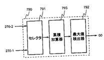
さらに、上記の実施形態において、被測定信号SINの信号対雑音比(SNR)が小さいような場合、雑音成分の方の影響が大きく、被測定信号SINに含まれる疑似雑音符号の正しい位相を検出できない場合がある。また、第三の実施形態では、部分相関の相関長を増やすことができるが、それでもなお正しい位相を検出できない場合がある。そのような問題を緩和するには、各実施形態において、PN符号発生器が発生する疑似雑音符号の位相ごと得られる相関値(累積加算結果)を、被測定信号SINに含まれる疑似雑音符号の1周期ごとに、さらに累積加算する回路を追加することが有効である。これにより、相関値のSNRが高まり、正しい位相を検出するようにすることができるようになる。例えば、第三の実施形態を変形する場合、図8における検出器690を、図11に示す検出器790に置き換えればよい。図11は、検出器790の内部構成の一例を示す図である。検出器790は、加算器270−1の出力データと加算器270−2の出力データのいずれかを選択して出力するセレクタ791と、セレクタ791の出力データを被測定信号SINに含まれる疑似雑音符号N3の1周期ごとに累積加算する累積加算器793と、累積加算器793から出力されるデータ(累積相関値)のうち絶対値が最大のものを検出し、当該最大値に対応する疑似雑音符号N3の位相を出力する最大値検出器792を備える。第一の実施形態および第二の実施形態においても同様である。
Further, in the above embodiment, when the signal to noise ratio (SNR) of the signal under test S IN is small, the influence of the noise component is large, and the correct phase of the pseudo noise code included in the signal under test S IN is large. May not be detected. In the third embodiment, the correlation length of the partial correlation can be increased, but there is still a case where a correct phase cannot be detected. To alleviate such a problem, in each embodiment, the correlation value (cumulative addition result) obtained for each phase of the pseudo noise code generated by the PN code generator is used as the pseudo noise code included in the signal under test S IN. It is effective to add a circuit for further cumulative addition every one cycle. As a result, the SNR of the correlation value is increased and the correct phase can be detected. For example, when the third embodiment is modified, the
またさらに、上記の各実施形態において、検出器は、加算器の出力データを参照するように構成されているが、累積のために加算器に接続されている遅延器の出力データを参照するようにしても良い。 Furthermore, in each of the above embodiments, the detector is configured to refer to the output data of the adder, but refers to the output data of the delay unit connected to the adder for accumulation. Anyway.
また、上記の各実施形態において、検出器は、被測定信号に含まれる疑似雑音符号の位相を検出するために累積加算結果の絶対値の最大値を検出しているが、最大値の検出に代えて所定の閾値レベルを超える累積加算結果を検出するようにしても良い。 In each of the above embodiments, the detector detects the maximum absolute value of the cumulative addition result in order to detect the phase of the pseudo noise code included in the signal under measurement. Instead, a cumulative addition result exceeding a predetermined threshold level may be detected.
さらに、上記の各実施形態において、相関長、または、被測定信号SINに含まれる疑似雑音符号の長さ、または、各符号発生装置が発生する疑似雑音符号の長さは、16ビットに限定されない。例えば、それらは、16ビットより短くても良いし、16ビットより長くても良い。例えば、38400チップの疑似雑音符号で拡散された被測定信号に対する128ビット長の部分相関であっても良い。 Furthermore, in each of the above embodiments, the correlation length, the length of the pseudo noise code included in the signal under test S IN , or the length of the pseudo noise code generated by each code generator is limited to 16 bits. Not. For example, they may be shorter than 16 bits or longer than 16 bits. For example, it may be a 128-bit partial correlation with a signal under measurement spread with a pseudo noise code of 38400 chips.
またさらに、上記の各実施形態において、PN符号発生器をゲートアレイ50内の記憶領域(不図示)やゲートアレイ50に接続されゲートアレイ50内と同等以上の速度でデータの読み出しが可能な記憶装置に置き換えることができる。すなわち、所望の疑似雑音符号データを当該記憶領域に予め格納しておき、その格納された疑似雑音符号を当該記憶領域から1ビットずつ順に繰り返し取り出すようにすれば良い。
Furthermore, in each of the above embodiments, the PN code generator is connected to a storage area (not shown) in the
また、上記の各実施形態において、各構成要素は、1つの筐体に備えられても良いし、2以上の筐体に分かれて備えられても良い。例えば、制御装置60が市販のコンピュータであって、その他の構成要素が、当該コンピュータに接続された1つの測定装置に備えられても良い。また、当該他の構成要素が当該市販のコンピュータに内蔵可能なボードあるいはカードに備えられても良い。
In each of the above embodiments, each component may be provided in one housing or may be provided in two or more housings. For example, the
本発明は、FPGAのような再構成可能なゲートアレイに限らず、ASICのようなカスタムLSIタイプのゲートアレイに対しても有益である。 The present invention is useful not only for a reconfigurable gate array such as an FPGA but also for a custom LSI type gate array such as an ASIC.
1,2,3 測定装置
10 入力端子
20 前処理装置
30 変換装置
40 記憶装置
50 ゲートアレイ
60 制御装置
70 出力端子
100 復調装置
200,400,600 同期捕捉装置
210,410 データ反復器
220,420 PN符号発生器
230−2 遅延器
240,440 カウンタ
250−1,250−2 ASR
260,460 乗算器
270,470 加算器
280,480 遅延器
290,490,690,790 検出器
310−0,310−1,310−2,310−3 フリップフロップ
310−4,310−5,310−6,310−7 フリップフロップ
320,520 セレクタ
430−2,430−3,430−4 遅延器
450−1,450−2,450−3,450−4 ASR
510−0,510−1,510−2,510−3 フリップフロップ
610−1,610−2 スイッチ
620 符号発生器
691,791 セレクタ
692,792 最大値検出器
793 累積加算器
1, 2, 3 Measuring device 10
260, 460 Multiplier 270, 470 Adder 280, 480
510-0, 510-1, 510-2, 510-3 Flip-flops 610-1, 610-2
Claims (18)
前記ゲートアレイを、
被測定信号に含まれる第一の疑似雑音符号と同じ符号系列であって、それぞれ位相が異なるK個の第二の疑似雑音符号を発生する疑似雑音符号発生器と、
前記K個のうち2以上のM個の前記第二の疑似雑音符号を選択対象とし、選択対象の前記第二の疑似雑音符号から1つを選択して出力する2以上のN個のセレクタであって、あるセレクタが選択対象とする前記第二の疑似雑音符号がその他のセレクタの選択対象外であるセレクタと、
各前記セレクタに個々に接続されるN個の乗算器であって、対応する前記セレクタが出力する前記第二の疑似雑音符号と前記第一の疑似雑音符号とを乗ずる乗算器と、
各前記乗算器に個々に接続されるN個の加算器であって、対応する前記乗算器が出力する乗算結果を前記乗算結果に対応する前記第二の疑似雑音符号の位相ごとに累積加算する加算器と、
前記加算器の加算結果のうち絶対値が最大である加算結果または所定閾値を超える加算結果に対応する前記第二の疑似雑音符号の位相を、前記第一の疑似雑音符号の位相として検出する検出器、
として機能するようにプログラムし、
各前記セレクタが、対応する前記乗算器に前記第一の疑似雑音符号の同一チップデータが供給されている間に、選択対象の前記第二の疑似雑音符号の全てが前記対応する乗算器に供給されるように、前記第二の疑似雑音符号を選択し、
前記測定装置が前記第一の疑似雑音符号に同期できるようにすることを特徴とするゲートアレイプログラム装置。 An apparatus for programming a reconfigurable gate array provided in a measurement apparatus,
The gate array;
A pseudo-noise code generator for generating K second pseudo-noise codes having the same code sequence as the first pseudo-noise code included in the signal under measurement, each having a different phase;
Two or more N selectors that select and output one or more of the second pseudo-noise codes of the two or more M of the K-numbers of the second pseudo-noise codes. A selector in which the second pseudo-noise code to be selected by a certain selector is not selected by other selectors;
N multipliers individually connected to each of the selectors, the multiplier for multiplying the second pseudo noise code output from the corresponding selector, and the first pseudo noise code;
N adders individually connected to each of the multipliers, wherein the multiplication results output from the corresponding multipliers are cumulatively added for each phase of the second pseudo noise code corresponding to the multiplication results. An adder;
Detection that detects the phase of the second pseudo noise code corresponding to the addition result having the maximum absolute value or the addition result exceeding a predetermined threshold among the addition results of the adder as the phase of the first pseudo noise code vessel,
Program to function as
While each of the selectors is supplied with the same chip data of the first pseudo noise code to the corresponding multiplier, all of the second pseudo noise codes to be selected are supplied to the corresponding multiplier. Selecting the second pseudo-noise code,
A gate array program device, characterized in that the measuring device can be synchronized with the first pseudo-noise code.
前記ゲートアレイを、
前記被測定信号に含まれる第一の疑似雑音符号と同じ符号系列であって、それぞれ位相が異なるK個の第二の疑似雑音符号を発生する疑似雑音符号発生器と、
前記K個のうち2以上のM個の前記第二の疑似雑音符号を選択対象とし、選択対象の前記第二の疑似雑音符号から1つを選択して出力する2以上のN個のセレクタであって、あるセレクタが選択対象とする前記第二の疑似雑音符号がその他のセレクタの選択対象外であるセレクタと、
各前記セレクタに個々に接続されるN個の乗算器であって、対応する前記セレクタが出力する前記第二の疑似雑音符号と前記記憶装置から読み出される前記被測定信号に含まれる前記第一の疑似雑音符号とを乗ずる乗算器と、
各前記乗算器に個々に接続されるN個の加算器であって、対応する前記乗算器が出力する乗算結果を前記乗算結果に対応する前記第二の疑似雑音符号の位相ごとに累積加算する加算器と、
前記加算器の加算結果のうち絶対値が最大である加算結果または所定閾値を超える加算結果に対応する前記第二の疑似雑音符号の位相を、前記第一の疑似雑音符号の位相として検出する検出器、
として機能するようにプログラムし、
各前記セレクタが、対応する前記乗算器に前記第一の疑似雑音符号の同一チップデータが供給されている間に、選択対象の前記第二の疑似雑音符号の全てが前記対応する乗算器に供給されるように、前記第二の疑似雑音符号を選択し、
前記測定装置が前記第一の疑似雑音符号に同期できるようにすることを特徴とするゲートアレイプログラム装置。 A device for programming a reconfigurable gate array, which is provided in a measuring device having a storage device for storing a signal under measurement and operates at a clock faster than a chip rate of the signal under measurement,
The gate array;
A pseudo-noise code generator for generating K second pseudo-noise codes having the same code sequence as the first pseudo-noise code included in the signal under measurement, each having a different phase;
Two or more N selectors that select and output one or more of the second pseudo-noise codes of the two or more M of the K-numbers of the second pseudo-noise codes. A selector in which the second pseudo-noise code to be selected by a certain selector is not selected by other selectors;
N multipliers individually connected to each of the selectors, wherein the first pseudo-noise code output from the corresponding selector and the first signal included in the signal under measurement read from the storage device A multiplier that multiplies the pseudo-noise code;
N adders individually connected to each of the multipliers, wherein the multiplication results output from the corresponding multipliers are cumulatively added for each phase of the second pseudo noise code corresponding to the multiplication results. An adder;
Detection that detects the phase of the second pseudo noise code corresponding to the addition result having the maximum absolute value or the addition result exceeding a predetermined threshold among the addition results of the adder as the phase of the first pseudo noise code vessel,
Program to function as
While each of the selectors is supplied with the same chip data of the first pseudo noise code to the corresponding multiplier, all of the second pseudo noise codes to be selected are supplied to the corresponding multiplier. Selecting the second pseudo-noise code,
A gate array program device, characterized in that the measuring device can be synchronized with the first pseudo-noise code.
各前記加算器が、対応する前記セレクタにおける前記第二の疑似雑音符号の選択周期と等しい時間遅延を有する第一の遅延器を用いて累積加算を行う、
ことを特徴とする請求項1または請求項2に記載のゲートアレイプログラム装置。 Each of the selectors periodically and repeatedly selects the second pseudo-noise code in a fixed order and timing;
Each of the adders performs cumulative addition using a first delay device having a time delay equal to a selection period of the second pseudo-noise code in the corresponding selector;
3. The gate array program device according to claim 1, wherein the gate array program device is a gate array program device.
前記ゲートアレイが、
被測定信号に含まれる第一の疑似雑音符号と同じ符号系列であって、それぞれ位相が異なるK個の第二の疑似雑音符号を発生する疑似雑音符号発生器と、
前記K個のうち2以上のM個の前記第二の疑似雑音符号を選択対象とし、選択対象の前記第二の疑似雑音符号から1つを選択して出力する2以上のN個のセレクタであって、あるセレクタが選択対象とする前記第二の疑似雑音符号がその他のセレクタの選択対象外であるセレクタと、
各前記セレクタに個々に接続されるN個の乗算器であって、対応する前記セレクタが出力する前記第二の疑似雑音符号と前記第一の疑似雑音符号とを乗ずる乗算器と、
各前記乗算器に個々に接続されるN個の加算器であって、対応する前記乗算器が出力する乗算結果を前記乗算結果に対応する前記第二の疑似雑音符号の位相ごとに累積加算する加算器と、
前記加算器の加算結果のうち絶対値が最大である加算結果または所定閾値を超える加算結果に対応する前記第二の疑似雑音符号の位相を、前記第一の疑似雑音符号の位相として検出する検出器、
として機能するようにプログラムされ、
各前記セレクタが、対応する前記乗算器に前記第一の疑似雑音符号の同一チップデータが供給されている間に、選択対象の前記第二の疑似雑音符号の全てが前記対応する乗算器に供給されるように、前記第二の疑似雑音符号を選択し、
前記測定装置が前記第一の疑似雑音符号に同期できるようにしたことを特徴とする測定装置。 A measuring device comprising a reconfigurable gate array,
The gate array is
A pseudo-noise code generator for generating K second pseudo-noise codes having the same code sequence as the first pseudo-noise code included in the signal under measurement, each having a different phase;
Two or more N selectors that select and output one or more of the second pseudo-noise codes of the two or more M of the K-numbers of the second pseudo-noise codes. A selector in which the second pseudo-noise code to be selected by a certain selector is not selected by other selectors;
N multipliers individually connected to each of the selectors, the multiplier for multiplying the second pseudo noise code output from the corresponding selector, and the first pseudo noise code;
N adders individually connected to each of the multipliers, wherein the multiplication results output from the corresponding multipliers are cumulatively added for each phase of the second pseudo noise code corresponding to the multiplication results. An adder;
Detection that detects the phase of the second pseudo noise code corresponding to the addition result having the maximum absolute value or the addition result exceeding a predetermined threshold among the addition results of the adder as the phase of the first pseudo noise code vessel,
Programmed to act as
While each of the selectors is supplied with the same chip data of the first pseudo noise code to the corresponding multiplier, all of the second pseudo noise codes to be selected are supplied to the corresponding multiplier. Selecting the second pseudo-noise code,
A measuring apparatus characterized in that the measuring apparatus can synchronize with the first pseudo-noise code.
前記ゲートアレイが、
前記被測定信号に含まれる第一の疑似雑音符号と同じ符号系列であって、それぞれ位相が異なるK個の第二の疑似雑音符号を発生する疑似雑音符号発生器と、
前記K個のうち2以上のM個の前記第二の疑似雑音符号を選択対象とし、選択対象の前記第二の疑似雑音符号から1つを選択して出力する2以上のN個のセレクタであって、あるセレクタが選択対象とする前記第二の疑似雑音符号がその他のセレクタの選択対象外であるセレクタと、
各前記セレクタに個々に接続されるN個の乗算器であって、対応する前記セレクタが出力する前記第二の疑似雑音符号と前記記憶装置から読み出される前記被測定信号に含まれる前記第一の疑似雑音符号とを乗ずる乗算器と、
各前記乗算器に個々に接続されるN個の加算器であって、対応する前記乗算器が出力する乗算結果を前記乗算結果に対応する前記第二の疑似雑音符号の位相ごとに累積加算する加算器と、
前記加算器の加算結果のうち絶対値が最大である加算結果または所定閾値を超える加算結果に対応する前記第二の疑似雑音符号の位相を、前記第一の疑似雑音符号の位相として検出する検出器、
として機能するようにプログラムされ、
各前記セレクタが、対応する前記乗算器に前記第一の疑似雑音符号の同一チップデータが供給されている間に、選択対象の前記第二の疑似雑音符号の全てが前記対応する乗算器に供給されるように、前記第二の疑似雑音符号を選択し、
前記測定装置が前記第一の疑似雑音符号に同期できるようにしたことを特徴とする測定装置。 A measuring device comprising a storage device for storing a signal under measurement, and a reconfigurable gate array operating at a clock faster than a chip rate of the signal under measurement,
The gate array is
A pseudo-noise code generator for generating K second pseudo-noise codes having the same code sequence as the first pseudo-noise code included in the signal under measurement, each having a different phase;
Two or more N selectors that select and output one or more of the second pseudo-noise codes of the two or more M of the K-numbers of the second pseudo-noise codes. A selector in which the second pseudo-noise code to be selected by a certain selector is not selected by other selectors;
N multipliers individually connected to each of the selectors, wherein the first pseudo-noise code output from the corresponding selector and the first signal included in the signal under measurement read from the storage device A multiplier that multiplies the pseudo-noise code;
N adders individually connected to each of the multipliers, wherein the multiplication results output from the corresponding multipliers are cumulatively added for each phase of the second pseudo noise code corresponding to the multiplication results. An adder;
Detection that detects the phase of the second pseudo noise code corresponding to the addition result having the maximum absolute value or the addition result exceeding a predetermined threshold among the addition results of the adder as the phase of the first pseudo noise code vessel,
Programmed to act as
While each of the selectors is supplied with the same chip data of the first pseudo noise code to the corresponding multiplier, all of the second pseudo noise codes to be selected are supplied to the corresponding multiplier. Selecting the second pseudo-noise code,
A measuring apparatus characterized in that the measuring apparatus can synchronize with the first pseudo-noise code.
各前記加算器が、対応する前記セレクタにおける前記第二の疑似雑音符号の選択周期と等しい時間遅延を有する第一の遅延器を用いて累積加算を行う、
ことを特徴とする請求項7または請求項8に記載の測定装置。 Each of the selectors periodically and repeatedly selects the second pseudo-noise code in a fixed order and timing;
Each of the adders performs cumulative addition using a first delay device having a time delay equal to a selection period of the second pseudo-noise code in the corresponding selector;
The measuring apparatus according to claim 7 or 8, wherein
前記プログラムされたゲートアレイが、
前記第一の疑似雑音符号と同じ符号系列であって、それぞれ位相が異なるK個の第二の疑似雑音符号を発生する疑似雑音符号発生器と、
前記K個のうち2以上のM個の前記第二の疑似雑音符号を選択対象とし、選択対象の前記第二の疑似雑音符号から1つを選択して出力する2以上のN個のセレクタであって、あるセレクタが選択対象とする前記第二の疑似雑音符号がその他のセレクタの選択対象外であるセレクタと、
各前記セレクタに個々に接続されるN個の乗算器であって、対応する前記セレクタが出力する前記第二の疑似雑音符号と前記第一の疑似雑音符号とを乗ずる乗算器と、
各前記乗算器に個々に接続されるN個の加算器であって、対応する前記乗算器が出力する乗算結果を前記乗算結果に対応する前記第二の疑似雑音符号の位相ごとに累積加算する加算器と、
前記加算器の加算結果のうち絶対値が最大である加算結果または所定閾値を超える加算結果に対応する前記第二の疑似雑音符号の位相を、前記第一の疑似雑音符号の位相として検出する検出器、
として機能し、
各前記セレクタが、対応する前記乗算器に前記第一の疑似雑音符号の同一チップデータが供給されている間に、選択対象の前記第二の疑似雑音符号の全てが前記対応する乗算器に供給されるように、前記第二の疑似雑音符号を選択する、
ことを特徴とするプログラム。 A program that causes a computer included in or connected to a measurement device having a reconfigurable gate array to program the gate array so that the measurement device is synchronized with a first pseudo-noise code included in the signal under measurement. There,
The programmed gate array is
A pseudo-noise code generator that generates K second pseudo-noise codes that are the same code sequence as the first pseudo-noise code, each having a different phase;
Two or more N selectors that select and output one or more of the second pseudo-noise codes of the two or more M of the K-numbers of the second pseudo-noise codes. A selector in which the second pseudo-noise code to be selected by a certain selector is not selected by other selectors;
N multipliers individually connected to each of the selectors, the multiplier for multiplying the second pseudo noise code output from the corresponding selector, and the first pseudo noise code;
N adders individually connected to each of the multipliers, wherein the multiplication results output from the corresponding multipliers are cumulatively added for each phase of the second pseudo noise code corresponding to the multiplication results. An adder;
Detection that detects the phase of the second pseudo noise code corresponding to the addition result having the maximum absolute value or the addition result exceeding a predetermined threshold among the addition results of the adder as the phase of the first pseudo noise code vessel,
Function as
While each of the selectors is supplied with the same chip data of the first pseudo noise code to the corresponding multiplier, all of the second pseudo noise codes to be selected are supplied to the corresponding multiplier. Selecting the second pseudo-noise code,
A program characterized by that.
前記プログラムされたゲートアレイが、
前記第一の疑似雑音符号と同じ符号系列であって、それぞれ位相が異なるK個の第二の疑似雑音符号を発生する疑似雑音符号発生器と、
前記K個のうち2以上のM個の前記第二の疑似雑音符号を選択対象とし、選択対象の前記第二の疑似雑音符号から1つを選択して出力する2以上のN個のセレクタであって、あるセレクタが選択対象とする前記第二の疑似雑音符号がその他のセレクタの選択対象外であるセレクタと、
各前記セレクタに個々に接続されるN個の乗算器であって、対応する前記セレクタが出力する前記第二の疑似雑音符号と前記記憶装置から読み出される前記被測定信号に含まれる前記第一の疑似雑音符号とを乗ずる乗算器と、
各前記乗算器に個々に接続されるN個の加算器であって、対応する前記乗算器が出力する乗算結果を前記乗算結果に対応する前記第二の疑似雑音符号の位相ごとに累積加算する加算器と、
前記加算器の加算結果のうち絶対値が最大である加算結果または所定閾値を超える加算結果に対応する前記第二の疑似雑音符号の位相を、前記第一の疑似雑音符号の位相として検出する検出器、
として機能し、
各前記セレクタが、対応する前記乗算器に前記第一の疑似雑音符号の同一チップデータが供給されている間に、選択対象の前記第二の疑似雑音符号の全てが前記対応する乗算器に供給されるように、前記第二の疑似雑音符号を選択する、
ことを特徴とするプログラム。 The signal to be measured is connected to a computer provided in or connected to a measuring device comprising a storage device for storing the signal to be measured and a reconfigurable gate array that operates at a clock faster than the chip rate of the signal to be measured. A program for programming the gate array so that the measurement device is synchronized with a first pseudo-noise code included in
The programmed gate array is
A pseudo-noise code generator that generates K second pseudo-noise codes that are the same code sequence as the first pseudo-noise code, each having a different phase;
Two or more N selectors that select and output one or more of the second pseudo-noise codes of the two or more M of the K-numbers of the second pseudo-noise codes. A selector in which the second pseudo-noise code to be selected by a certain selector is not selected by other selectors;
N multipliers individually connected to each of the selectors, wherein the first pseudo-noise code output from the corresponding selector and the first signal included in the signal under measurement read from the storage device A multiplier that multiplies the pseudo-noise code;
N adders individually connected to each of the multipliers, wherein the multiplication results output from the corresponding multipliers are cumulatively added for each phase of the second pseudo noise code corresponding to the multiplication results. An adder;
Detection that detects the phase of the second pseudo noise code corresponding to the addition result having the maximum absolute value or the addition result exceeding a predetermined threshold among the addition results of the adder as the phase of the first pseudo noise code vessel,
Function as
While each of the selectors is supplied with the same chip data of the first pseudo noise code to the corresponding multiplier, all of the second pseudo noise codes to be selected are supplied to the corresponding multiplier. Selecting the second pseudo-noise code,
A program characterized by that.
各前記加算器が、対応する前記セレクタにおける前記第二の疑似雑音符号の選択周期と等しい時間遅延を有する第一の遅延器を用いて累積加算を行う、
ことを特徴とする請求項13または請求項14に記載のプログラム。 Each of the selectors periodically and repeatedly selects the second pseudo-noise code in a fixed order and timing;
Each of the adders performs cumulative addition using a first delay device having a time delay equal to a selection period of the second pseudo-noise code in the corresponding selector;
15. The program according to claim 13 or claim 14, characterized in that:
Priority Applications (3)
| Application Number | Priority Date | Filing Date | Title |
|---|---|---|---|
| JP2005361205A JP2007166350A (en) | 2005-12-15 | 2005-12-15 | Gate array program unit, measurement unit, and program |
| US11/541,883 US20070140324A1 (en) | 2005-12-15 | 2006-10-02 | Apparatus for FPGA Programming to synchronize with CDMA signals |
| DE200610054466 DE102006054466A1 (en) | 2005-12-15 | 2006-11-18 | FPGA programming device for synchronizing with CDMA signals |
Applications Claiming Priority (1)
| Application Number | Priority Date | Filing Date | Title |
|---|---|---|---|
| JP2005361205A JP2007166350A (en) | 2005-12-15 | 2005-12-15 | Gate array program unit, measurement unit, and program |
Publications (2)
| Publication Number | Publication Date |
|---|---|
| JP2007166350A true JP2007166350A (en) | 2007-06-28 |
| JP2007166350A5 JP2007166350A5 (en) | 2009-02-05 |
Family
ID=38108996
Family Applications (1)
| Application Number | Title | Priority Date | Filing Date |
|---|---|---|---|
| JP2005361205A Pending JP2007166350A (en) | 2005-12-15 | 2005-12-15 | Gate array program unit, measurement unit, and program |
Country Status (3)
| Country | Link |
|---|---|
| US (1) | US20070140324A1 (en) |
| JP (1) | JP2007166350A (en) |
| DE (1) | DE102006054466A1 (en) |
Families Citing this family (3)
| Publication number | Priority date | Publication date | Assignee | Title |
|---|---|---|---|---|
| US7547847B2 (en) * | 2006-09-19 | 2009-06-16 | Siemens Energy, Inc. | High thermal conductivity dielectric tape |
| CN103023529B (en) * | 2012-12-05 | 2014-08-20 | 天津光电通信技术有限公司 | Field programmable gate array (FPGA) based method for achieving synchronous detection of oversampling Golay sequence |
| CN109586760B (en) * | 2018-12-10 | 2021-04-27 | 湖北航天技术研究院总体设计所 | Wireless communication method and system suitable for narrow pulse signals |
Citations (2)
| Publication number | Priority date | Publication date | Assignee | Title |
|---|---|---|---|---|
| JPH11112384A (en) * | 1997-09-30 | 1999-04-23 | Sony Corp | Synchronism acquisition device and reception device for pseudo-noise code |
| JP2002009672A (en) * | 2000-05-05 | 2002-01-11 | Lucent Technol Inc | Increase of cell size for time-effective real-time correlation unit for cdma system |
Family Cites Families (6)
| Publication number | Priority date | Publication date | Assignee | Title |
|---|---|---|---|---|
| JP3825179B2 (en) * | 1998-07-17 | 2006-09-20 | 富士通株式会社 | Correlator |
| KR100513710B1 (en) * | 1999-05-25 | 2005-09-07 | 삼성전자주식회사 | Method and apparatus for performing code acquisition in CDMA communications system |
| US6801564B2 (en) * | 2000-02-23 | 2004-10-05 | Ipr Licensing, Inc. | Reverse link correlation filter in wireless communication systems |
| US6724810B1 (en) * | 2000-11-17 | 2004-04-20 | Xilinx, Inc. | Method and apparatus for de-spreading spread spectrum signals |
| US7224721B2 (en) * | 2002-10-11 | 2007-05-29 | The Mitre Corporation | System for direct acquisition of received signals |
| US7167504B1 (en) * | 2003-01-27 | 2007-01-23 | L-3 Communications Corporation | System and method for fast data rate discovery from PN codes |
-
2005
- 2005-12-15 JP JP2005361205A patent/JP2007166350A/en active Pending
-
2006
- 2006-10-02 US US11/541,883 patent/US20070140324A1/en not_active Abandoned
- 2006-11-18 DE DE200610054466 patent/DE102006054466A1/en not_active Withdrawn
Patent Citations (2)
| Publication number | Priority date | Publication date | Assignee | Title |
|---|---|---|---|---|
| JPH11112384A (en) * | 1997-09-30 | 1999-04-23 | Sony Corp | Synchronism acquisition device and reception device for pseudo-noise code |
| JP2002009672A (en) * | 2000-05-05 | 2002-01-11 | Lucent Technol Inc | Increase of cell size for time-effective real-time correlation unit for cdma system |
Also Published As
| Publication number | Publication date |
|---|---|
| US20070140324A1 (en) | 2007-06-21 |
| DE102006054466A1 (en) | 2007-06-28 |
Similar Documents
| Publication | Publication Date | Title |
|---|---|---|
| EP2294518B1 (en) | Adaptive correlation | |
| US5715276A (en) | Symbol-matched filter having a low silicon and power requirement | |
| RU2007108199A (en) | METHOD AND DEVICE FOR PROCESSING A RECEIVED SIGNAL IN A COMMUNICATION SYSTEM | |
| KR20000029073A (en) | Method and apparatus for generating multiple matched-filter vectors in a CDMA demodulator | |
| KR20050053720A (en) | System and method for detecting direct sequence spread spectrum signals using pipelined vector processing | |
| KR100268445B1 (en) | Receiver for spread spectrum coomunication system capable of shortening an acquisition time | |
| JP2006270510A (en) | Receiver and method for demodulating signal | |
| JP2007166350A (en) | Gate array program unit, measurement unit, and program | |
| JP2004254326A (en) | Dual mode modem and its method for performing integration cell search | |
| US20070002933A1 (en) | Parallel correlator implementation using block integration for spread-spectrum communication | |
| JP2001094468A (en) | Correlator | |
| KR101157108B1 (en) | Correlator for primary cell search using memory architecture | |
| JP2000036774A (en) | Correlation detector and cdma receiver | |
| JP3333454B2 (en) | Correlation detecting device and despreading code switching method of correlation detecting device | |
| JP3869674B2 (en) | Sliding correlator for spread spectrum communication | |
| JP4358161B2 (en) | Spreading code and timing detection apparatus and method | |
| JP2002305466A (en) | Rake receiving apparatus | |
| JP2000209124A (en) | Correlation circuit for spread spectrum communication | |
| JP4034571B2 (en) | Synchronization detection circuit | |
| JP2914312B2 (en) | Synchronous acquisition circuit | |
| JP2596988B2 (en) | Spread spectrum communication system and apparatus | |
| US20080130546A1 (en) | Hardware-Efficient Searcher Architecture For Cdma Cellular Receivers | |
| JP2007110691A (en) | Correlative demodulator and correlative demodulation method | |
| US7061975B2 (en) | Noncyclic digital filter and radio reception apparatus comprising the filter | |
| Bahl | Designing hardware efficient acquisition units for initial cell search in WCDMA |
Legal Events
| Date | Code | Title | Description |
|---|---|---|---|
| A521 | Written amendment |
Free format text: JAPANESE INTERMEDIATE CODE: A523 Effective date: 20081211 |
|
| A621 | Written request for application examination |
Free format text: JAPANESE INTERMEDIATE CODE: A621 Effective date: 20081211 |
|
| A131 | Notification of reasons for refusal |
Free format text: JAPANESE INTERMEDIATE CODE: A131 Effective date: 20111004 |
|
| A02 | Decision of refusal |
Free format text: JAPANESE INTERMEDIATE CODE: A02 Effective date: 20120229 |