JP2007140733A - Semiconductor processor and semiconductor integrated circuit - Google Patents
Semiconductor processor and semiconductor integrated circuit Download PDFInfo
- Publication number
- JP2007140733A JP2007140733A JP2005331334A JP2005331334A JP2007140733A JP 2007140733 A JP2007140733 A JP 2007140733A JP 2005331334 A JP2005331334 A JP 2005331334A JP 2005331334 A JP2005331334 A JP 2005331334A JP 2007140733 A JP2007140733 A JP 2007140733A
- Authority
- JP
- Japan
- Prior art keywords
- page
- data
- memory
- byte
- mat
- Prior art date
- Legal status (The legal status is an assumption and is not a legal conclusion. Google has not performed a legal analysis and makes no representation as to the accuracy of the status listed.)
- Withdrawn
Links
Images


Classifications
-
- G—PHYSICS
- G11—INFORMATION STORAGE
- G11C—STATIC STORES
- G11C7/00—Arrangements for writing information into, or reading information out from, a digital store
- G11C7/10—Input/output [I/O] data interface arrangements, e.g. I/O data control circuits, I/O data buffers
- G11C7/1006—Data managing, e.g. manipulating data before writing or reading out, data bus switches or control circuits therefor
-
- G—PHYSICS
- G06—COMPUTING; CALCULATING OR COUNTING
- G06F—ELECTRIC DIGITAL DATA PROCESSING
- G06F12/00—Accessing, addressing or allocating within memory systems or architectures
- G06F12/02—Addressing or allocation; Relocation
- G06F12/0223—User address space allocation, e.g. contiguous or non contiguous base addressing
- G06F12/023—Free address space management
- G06F12/0238—Memory management in non-volatile memory, e.g. resistive RAM or ferroelectric memory
- G06F12/0246—Memory management in non-volatile memory, e.g. resistive RAM or ferroelectric memory in block erasable memory, e.g. flash memory
-
- G—PHYSICS
- G11—INFORMATION STORAGE
- G11C—STATIC STORES
- G11C16/00—Erasable programmable read-only memories
- G11C16/02—Erasable programmable read-only memories electrically programmable
- G11C16/06—Auxiliary circuits, e.g. for writing into memory
- G11C16/10—Programming or data input circuits
- G11C16/102—External programming circuits, e.g. EPROM programmers; In-circuit programming or reprogramming; EPROM emulators
-
- Y—GENERAL TAGGING OF NEW TECHNOLOGICAL DEVELOPMENTS; GENERAL TAGGING OF CROSS-SECTIONAL TECHNOLOGIES SPANNING OVER SEVERAL SECTIONS OF THE IPC; TECHNICAL SUBJECTS COVERED BY FORMER USPC CROSS-REFERENCE ART COLLECTIONS [XRACs] AND DIGESTS
- Y02—TECHNOLOGIES OR APPLICATIONS FOR MITIGATION OR ADAPTATION AGAINST CLIMATE CHANGE
- Y02D—CLIMATE CHANGE MITIGATION TECHNOLOGIES IN INFORMATION AND COMMUNICATION TECHNOLOGIES [ICT], I.E. INFORMATION AND COMMUNICATION TECHNOLOGIES AIMING AT THE REDUCTION OF THEIR OWN ENERGY USE
- Y02D10/00—Energy efficient computing, e.g. low power processors, power management or thermal management
Landscapes
- Engineering & Computer Science (AREA)
- Theoretical Computer Science (AREA)
- Physics & Mathematics (AREA)
- General Engineering & Computer Science (AREA)
- General Physics & Mathematics (AREA)
- Read Only Memory (AREA)
- Memory System (AREA)
- Techniques For Improving Reliability Of Storages (AREA)
Abstract
Description
本発明は、書換え可能な不揮発性メモリを備えた半導体集積回路、そして、書換え可能な不揮発性メモリと前記不揮発性メモリをアクセス可能なデータ処理ユニットとを有する半導体処理装置に係り、例えばICカード用マイクロコンピュータ等に適用して有効な技術に関する。 The present invention relates to a semiconductor integrated circuit including a rewritable nonvolatile memory, and a semiconductor processing apparatus having a rewritable nonvolatile memory and a data processing unit capable of accessing the nonvolatile memory, for example, for an IC card. The present invention relates to a technology effective when applied to a microcomputer or the like.
特許文献1には、CPUと共に電気的に書換え可能なEEPROMを備え、EEPROMをデータ領域及びプログラム領域の双方に利用するようにしたICカード用マイクロコンピュータについて記載がある。特許文献2には電気的に書換え可能なフラッシュメモリをCPUと共にオンチップしたマイクロコンピュータについて記載がある。特許文献3には、同一メモリセル構成のFlashメモリとEEPROMとを有するICカード用マイクロコンピュータについて記載がある。マイクロコンピュータにおいてデータ記憶領域として利用されるEEPROMやフラッシュメモリに対しては、データ処理上、所要の時間内にデータの書き換えが可能であることが要求される。EEPROMもフラッシュメモリも共に電気的に消去及び書込み可能な不揮発性メモリセルを用いて構成される点は同じである。EEPROMは消去及び書込み単位であるバイト単位で不揮発性メモリセルのウェル領域を電気的に分離して構成される。これにより、ウェル領域とコントロールゲートの間に高電圧を印加してバイト単位消去を行い、また、ドレインとコントロールゲートの間に高電圧を印加してバイト単位の書き込みを行うことができるようになっている。消去及び書込み対象外のバイトデータには消去・書込み動作は一切行われない。一方、フラッシュメモリは、バイト単位のウェル分離を行わず、ページ単位即ちワード線単位でウェル領域とコントロールゲートの間に高電圧を印加してワード線単位の一括消去を行う。書き込みはワード線単位でコントロールゲートに高電圧を印加して行うようになっている。したがって、フラッシュメモリでバイトデータを書換える場合は、書換え動作の対象とされるワード線1本分の記憶情報をデータラッチに退避し、退避した後に当該ワード線を単位として一括消去を行う。この後、退避したデータラッチ上における書換えられるべきバイトデータを外部からの書き込みバイトデータに置き換え、置き換えが行われた1ワード線分のデータを用いてワード線単位の書き込みを行う。
Patent Document 1 describes an IC card microcomputer that includes an electrically rewritable EEPROM together with a CPU and uses the EEPROM for both a data area and a program area.
本発明者はEEPROMをフラッシュメモリに置き換えることを検討した。即ち、EEPROMはバイト単位で不揮発性メモリセルのウェル領域分離が行われているためバイト単位の書き換えを直接行うことができるが、チップ面積が大きくなってしまう。そこで、バイト単位のウェル領域分離が行われていないフラッシュメモリを採用することにより、チップ面積の40%程度の小型化、或いは記憶容量の増大を企図した。しかしながら、消去書込み単位がページ単位例えばワード線単位とされるフラッシュメモリにおいてバイト単位の書き換えを行うには、消去前にワード線単位でデータラッチに退避したデータが動作電源等の遮断によって不所望に破壊されるのを抑制することが必要になる。そのためには、退避したデータを不揮発性メモリ領域に一次的にバックアップしたりする動作を行わなければならない。この動作をデータの書換えの度にCPUのソフトウェアで行っていたのでは書換え動作時間が長くかかり過ぎてしまう。例えば非接触インタフェースを行うカードデバイスに用いるICカード用マイクロコンピュータのような用途では、限られた非接触インタフェース時間内にフラッシュメモリの書き換え等を行わなければならないから、動作の高速化が要求される。 The inventor has considered replacing the EEPROM with a flash memory. That is, since the EEPROM performs well region isolation of the nonvolatile memory cells in byte units, rewriting in byte units can be performed directly, but the chip area increases. Therefore, by adopting a flash memory in which the well region separation is not performed in byte units, an attempt was made to reduce the chip area by about 40% or increase the storage capacity. However, in the flash memory in which the erasing / writing unit is a page unit, for example, a word line unit, in order to perform byte unit rewriting, the data saved in the data latch in word line units before erasing is undesirably caused by shutting off the operation power It is necessary to suppress destruction. For this purpose, an operation for temporarily backing up the saved data in the nonvolatile memory area must be performed. If this operation is performed by software of the CPU every time data is rewritten, the rewriting operation time takes too long. For example, in applications such as a microcomputer for an IC card used for a card device that performs a non-contact interface, the flash memory must be rewritten within a limited non-contact interface time. .
本発明の目的は、不揮発性メモリの消去対象とされる記憶情報をバックアップするのに要する時間を短縮することができる半導体処理装置並びに半導体集積回路を提供することにある。 An object of the present invention is to provide a semiconductor processing apparatus and a semiconductor integrated circuit that can reduce the time required to back up stored information to be erased from a nonvolatile memory.
本発明の前記並びにその他の目的と新規な特徴は本明細書の記述及び添付図面から明らかになるであろう。 The above and other objects and novel features of the present invention will be apparent from the description of this specification and the accompanying drawings.
本願において開示される発明のうち代表的なものの概要を簡単に説明すれば下記の通りである。 The following is a brief description of an outline of typical inventions disclosed in the present application.
〔1〕本発明に係る半導体処理装置(1)は、書換え可能な不揮発性メモリ(6)と、前記不揮発性メモリをアクセス可能なデータ処理ユニット(2)とを有する。前記不揮発性メモリは、ページ単位で書換え動作が可能にされる複数のメモリマット(21,22)と、前記データ処理ユニットからのアクセス指示に応答して前記メモリマットに対するメモリ動作を制御するメモリ制御回路(26,37,38)とを有する。前記メモリ制御回路はメモリマットの所定のアドレス領域に対するアクセスに応答してバイトアクセス制御を行い、その他のアドレス領域に対するアクセスに応答してページアクセス制御を行う。前記メモリ制御回路はバイトアクセス制御において複数のメモリマットの各々のページから当該ページの管理情報を読み出し、読み出した管理情報から有効ページの中で最も最近書換えられたページを判定し、データ書き換えでは前記判定したページから読出したデータをバイト単位の書込みデータでマージし、マージしたデータを他のメモリマットの中で選択した対応ページに書き込み、読出しでは前記判定されたページから読出しを行う。 [1] A semiconductor processing apparatus (1) according to the present invention includes a rewritable nonvolatile memory (6) and a data processing unit (2) capable of accessing the nonvolatile memory. The nonvolatile memory includes a plurality of memory mats (21, 22) that can be rewritten on a page-by-page basis, and a memory control that controls a memory operation on the memory mat in response to an access instruction from the data processing unit. Circuit (26, 37, 38). The memory control circuit performs byte access control in response to access to a predetermined address area of the memory mat, and performs page access control in response to access to other address areas. The memory control circuit reads the management information of the page from each page of a plurality of memory mats in byte access control, determines the most recently rewritten page among the valid pages from the read management information. Data read from the determined page is merged with write data in units of bytes, the merged data is written to the corresponding page selected in another memory mat, and reading is performed from the determined page.
上記した手段によれば、バイトアクセス制御によるデータの書換え動作では、一のメモリマットの中で選択された最も最近書換えられた有効ページには書換え対象バイト以外のデータがそのまま保存され、他のメモリマットの中で選択されたページには書換え対象バイトが更新されたページデータが新たに書き込まれることになる。したがって、一のメモリマットの中で選択されたページは他のメモリマットの中で選択されたページに対して書換え前の実質的なバックアップデータを保有することになる。バックアップのために別の領域にデータを転送するための別のアクセス動作を追加することを要しない。読出しにおいてバックアップページなのか正規ページなのかは、各々のページの管理情報より、最も最近書換えられたページであるか否かを判定することによって区別される。 According to the above-described means, in the data rewrite operation by byte access control, data other than the rewrite target byte is stored as it is in the most recently rewritten valid page selected in one memory mat, and other memory is stored. The page data in which the rewrite target byte is updated is newly written in the page selected in the mat. Therefore, the page selected in one memory mat holds substantial backup data before rewriting with respect to the page selected in the other memory mat. It is not necessary to add another access operation for transferring data to another area for backup. Whether the page is a backup page or a regular page is determined by determining whether the page is the most recently rewritten page from the management information of each page.
本発明の具体的な一つの形態として、前記管理情報として、当該ページが保有するデータが破壊されているか否かを示すための複数ビットのエラー判定ビット(PDS2,PDS3)を含む。前記メモリ制御回路は前記選択されたページの有効性を当該ページが保有する前記エラー判定ビットによって判定する。 As a specific form of the present invention, the management information includes a plurality of error determination bits (PDS2, PDS3) for indicating whether or not the data held by the page is destroyed. The memory control circuit determines the validity of the selected page by the error determination bit held by the page.
本発明の更に具体的な形態として、前記エラー判定ビットは全ビット同一論理値以外の複数の論理値の組み合わせを有する。消去又は書込み途中の電源遮断等によるデータ破壊があれば、複数ビットのエラー判定ビットは共に論理値0又は1の同じ論理値になると考えられるからである。 As a more specific form of the invention, the error determination bit has a combination of a plurality of logical values other than the same logical value of all bits. This is because if there is data destruction due to power interruption or the like during erasing or writing, the error determination bits of a plurality of bits are considered to have the same logical value of logical value 0 or 1.
本発明の更に具体的な形態として、前記メモリ制御回路は、前記マージしたデータを書込む前記対応ページの有効無効を問わない。 As a more specific form of the present invention, the memory control circuit does not matter whether the corresponding page into which the merged data is written is valid or invalid.
本発明の更に具体的な形態として、前記管理情報として当該ページが保有するデータの優先度を示すための複数ビットの優先度データ(PDS0,PDS1)を有する。前記制御回路は、優先度の高い優先度データに対応するページほど最近書換えられたページであると判定する。 As a more specific form of the present invention, the management information includes multi-bit priority data (PDS0, PDS1) for indicating the priority of data held by the page. The control circuit determines that a page corresponding to priority data having a higher priority is a page that has been recently rewritten.
本発明の更に具体的な形態として、前記メモリ制御回路は、前記バイトデータをマージしたデータの書き込みにおいて、書込み対象ページの優先度データを、前記バイトデータによるマージ対象とされた元のデータを保有するページの優先度よりも高い優先度に更新する。これにより、最も最近書換えられたページか否かを判定可能なように優先度データを更新する操作が容易になる。 As a more specific form of the present invention, the memory control circuit retains the priority data of the write target page and the original data to be merged by the byte data in writing the data obtained by merging the byte data. To a higher priority than the priority of the page to be updated. This facilitates the operation of updating the priority data so that it can be determined whether the page has been most recently rewritten.
本発明の別の具体的な一つの形態として、前記バイトアクセス制御の対象とされる前記所定のアドレス領域はデータ格納領域とされ、前記ページアクセス制御の対象とされる前記その他のアドレス領域はプログラム格納領域とされる。データアクセスに対しては書込みであっても高速アクセスの要求を満足することが必要になるが、プログラムに関してはデータ処理途上で高速に書換えなければならない事情は殆どないことを考慮し、アドレスマッピング可能なプログラムメモリ容量の増大を最優先させたものである。 As another specific mode of the present invention, the predetermined address area subject to the byte access control is a data storage area, and the other address area subject to the page access control is a program. It is a storage area. For data access, it is necessary to satisfy the requirement for high-speed access even for writing, but address mapping is possible in consideration of the fact that there is almost no need to rewrite the program at high speed during data processing. The increase in program memory capacity is given top priority.
本発明の更に別の具体的な一つの形態として、前記バイトアクセス制御の対象とされる前記所定のアドレス領域は第1のデータ格納領域とされ、前記ページアクセス制御の対象とされる前記その他のアドレス領域は第2のデータ格納領域とされる。メモリセル数に対するアドレスマッピング容量は第2のデータ領域に比べて第1のデータ領域は半減する。しかしながら、最大書換え保証回数は第2のデータ領域に比べて第1のデータ領域は倍増する。 As yet another specific mode of the present invention, the predetermined address area that is subject to byte access control is a first data storage area, and the other address areas that are subject to page access control. The address area is a second data storage area. The address mapping capacity with respect to the number of memory cells is halved in the first data area compared to the second data area. However, the maximum number of rewrite guarantees is doubled in the first data area compared to the second data area.
本発明の更に別の具体的な一つの形態として、前記メモリ制御回路はアドレス制御部(37)を有する。前記アドレス制御部は、前記データ処理ユニットから供給されるアクセスアドレス信号(ADRS)を入力し、入力したアクセスアドレス信号に対してページを選択するページ選択アドレス(XADRS)とページ内のバイトを選択するバイト選択アドレス(YADRS)と、2ビットのマット選択制御信号(MC1,MC2)とを生成する。前記アドレス制御部は、前記ページアクセス制御を指定する前記アクセスアドレス信号に対しては2個のメモリマットに共通のページアドレスを生成すると共に前記アクセスアドレス信号の所定の1ビットの値に応じて前記マット選択制御信号を第1の値又は第2の値とし、前記バイトアクセス制御を指定する前記アクセスアドレス信号対しては2個のメモリマットに共通のページアドレスを生成すると共にその他の制御情報に基づいて前記選択制御信号を第3の値又は第4の値とする。前記メモリ制御回路は、前記マット選択制御信号が第3の値のときは前記最も最近書換えられたと判定されたページから読出しを行う。 As yet another specific mode of the present invention, the memory control circuit includes an address control unit (37). The address control unit inputs an access address signal (ADRS) supplied from the data processing unit, and selects a page selection address (XADRS) for selecting a page and a byte in the page with respect to the input access address signal. A byte selection address (YADRS) and a 2-bit mat selection control signal (MC1, MC2) are generated. The address control unit generates a page address common to two memory mats for the access address signal designating the page access control and according to a predetermined 1-bit value of the access address signal A mat selection control signal is set to a first value or a second value, and for the access address signal designating the byte access control, a page address common to two memory mats is generated and based on other control information The selection control signal is set to the third value or the fourth value. The memory control circuit reads from the page determined to be the most recently rewritten when the mat selection control signal has a third value.
前記その他の制御情報は、例えば、選択的にテストモードを設定するための制御情報である。更に具体的形態として、前記メモリ制御回路は、前記選択制御信号が第4の値のときは前記判定されたページとは異なるページから読出しを行う。外部に読み出されないバックアップ側のページデータに検証等のようなテスト動作に用いることができる。 The other control information is, for example, control information for selectively setting a test mode. As a more specific form, the memory control circuit reads from a page different from the determined page when the selection control signal is a fourth value. It can be used for test operations such as verification of backup page data that is not read externally.
本発明の更に別の具体的な一つの形態として、前記バイトアクセス制御を行うメモリマットの所定のアドレス領域は、アクセス不可能な領域とアクセス可能な領域とに2分割された領域である。これに対応するには、ページ選択を行うアドレス信号(XADRS)をデコードするデコード論理は、ページアクセスだけのデコード論理に対して1ビット少ないアドレス情報に対するデコード論理を持つことが必要になり、これに応じてアドレス制御回路(37)はCPU等からのアクセスアドレス信号(ADRS)から必要なアドレス信号(XADRS)を切り出すときその上位側アドレスビットの1ビットを削除することが必要になる。 As yet another specific mode of the present invention, the predetermined address area of the memory mat for performing the byte access control is an area divided into an inaccessible area and an accessible area. In order to cope with this, the decoding logic for decoding the address signal (XADRS) for page selection needs to have a decoding logic for address information that is one bit less than the decoding logic for page access only. Accordingly, when the address control circuit (37) cuts out the necessary address signal (XADRS) from the access address signal (ADRS) from the CPU or the like, it is necessary to delete one bit of the higher-order address bits.
別の形態として、前記バイトアクセス制御を行うメモリマットの所定のアドレス領域は、アクセス不可とアクセス可能な領域がページ毎に交互に配置された領域としてもよい。この場合は、ページ選択を行うアドレス信号(XADRS)をデコードするデコード論理は、ページアクセスだけのデコード論理と同じであってよく、アドレス制御回路もCPU等からのアクセスアドレス信号の上位側から必要なアドレス信号を単に切り出して出力すればよい。従って、アドレス制御回路にデータ格納領域を設定するレジスタを設け、ソフトにてレジスタの値を書換えデータ格納領域を設定できる。 As another form, the predetermined address area of the memory mat that performs the byte access control may be an area in which inaccessible and accessible areas are alternately arranged for each page. In this case, the decoding logic for decoding the address signal (XADRS) for page selection may be the same as the decoding logic for page access only, and the address control circuit is also required from the upper side of the access address signal from the CPU or the like. What is necessary is just to cut out and output an address signal. Therefore, a register for setting the data storage area is provided in the address control circuit, and the data storage area can be set by rewriting the value of the register by software.
〔2〕本発明の別の観点による半導体処理装置は、書換え可能な不揮発性メモリと、前記不揮発性メモリをアクセス可能なデータ処理ユニットとを有する。前記不揮発性メモリは、ページ単位で書換え動作が可能にされる複数のメモリマットと、前記データ処理ユニットからのアクセス指示に応答して前記メモリマットに対するバイトアクセス制御が可能なメモリ制御回路とを有する。前記メモリ制御回路はバイトアクセス制御において複数のメモリマットの各々のページから当該ページの管理情報を読み出し、読み出した管理情報から有効ページの中で最も最近書換えられたページを判定し、データ書き換えでは前記判定したページから読出したデータをバイト単位の書込みデータでマージし、マージしたデータを他のメモリマットの中で選択した対応ページに書き込み、読出しでは前記判定されたページから読出しを行う。 [2] A semiconductor processing apparatus according to another aspect of the present invention includes a rewritable nonvolatile memory and a data processing unit capable of accessing the nonvolatile memory. The nonvolatile memory includes a plurality of memory mats that can be rewritten in units of pages, and a memory control circuit that can perform byte access control on the memory mat in response to an access instruction from the data processing unit. . The memory control circuit reads the management information of the page from each page of a plurality of memory mats in byte access control, determines the most recently rewritten page among the valid pages from the read management information. Data read from the determined page is merged with write data in units of bytes, the merged data is written to the corresponding page selected in another memory mat, and reading is performed from the determined page.
上記した手段によれば、バイトアクセス制御によるデータの書換え動作では、一のメモリマットの中で選択された最も最近書換えられた有効ページには書換え対象バイト以外のデータがそのまま保存され、他のメモリマットの中で選択されたページには書換え対象バイトが更新されたページデータが新たに書き込まれることになる。したがって、一のメモリマットの中で選択されたページは他のメモリマットの中で選択されたページに対して書換え前の実質的なバックアップデータを保有することになる。バックアップのために別の領域にデータを転送するための別のアクセス動作を追加することを要しない。読出しにおいてバックアップページなのか正規ページなのかは、各々のページの管理情報より、最も最近書換えられたページであるか否かを判定することによって区別される。 According to the above-described means, in the data rewrite operation by byte access control, data other than the rewrite target byte is stored as it is in the most recently rewritten valid page selected in one memory mat, and other memory is stored. The page data in which the rewrite target byte is updated is newly written in the page selected in the mat. Therefore, the page selected in one memory mat holds substantial backup data before rewriting with respect to the page selected in the other memory mat. It is not necessary to add another access operation for transferring data to another area for backup. Whether the page is a backup page or a regular page is determined by determining whether the page is the most recently rewritten page from the management information of each page.
〔3〕本発明の別の観点による半導体集積回路は、書換え可能な不揮発性メモリを有する。前記不揮発性メモリは、ページ単位で書換え動作が可能にされる複数のメモリマットと、外部からのアクセス指示に応答して前記メモリマットに対するバイトアクセス制御を行うメモリ制御回路とを有する。前記メモリ制御回路はバイトアクセス制御において複数のメモリマットの各々のページから当該ページの管理情報を読み出し、読み出した管理情報から有効ページの中で最も最近書換えられたページを判定し、データ書き換えでは前記判定したページから読出したデータをバイト単位の書込みデータでマージし、マージしたデータを他のメモリマットの中で選択した対応ページに書き込み、読出しでは前記判定されたページから読出しを行う。 [3] A semiconductor integrated circuit according to another aspect of the present invention has a rewritable nonvolatile memory. The nonvolatile memory includes a plurality of memory mats that can be rewritten in units of pages, and a memory control circuit that performs byte access control on the memory mats in response to an access instruction from the outside. The memory control circuit reads the management information of the page from each page of a plurality of memory mats in byte access control, determines the most recently rewritten page among the valid pages from the read management information. Data read from the determined page is merged with write data in units of bytes, the merged data is written to the corresponding page selected in another memory mat, and reading is performed from the determined page.
上記同様に、バイトアクセス制御によるデータの書換え動作では、一のメモリマットの中で選択された最も最近書換えられた有効ページには書換え対象バイト以外のデータがそのまま保存され、他のメモリマットの中で選択されたページには書換え対象バイトが更新されたページデータが新たに書き込まれることになる。したがって、一のメモリマットの中で選択されたページは他のメモリマットの中で選択されたページに対して書換え前の実質的なバックアップデータを保有することになる。 Similarly to the above, in the data rewrite operation by byte access control, the data other than the byte to be rewritten is stored as it is in the most recently rewritten valid page selected in one memory mat, and is stored in another memory mat. The page data in which the rewrite target byte is updated is newly written in the page selected in step (b). Therefore, the page selected in one memory mat holds substantial backup data before rewriting with respect to the page selected in the other memory mat.
〔4〕本発明の別の観点による半導体集積回路は、書換え可能な不揮発性メモリを有する。前記不揮発性メモリは、ページ単位で書換え動作が可能にされる複数のメモリマットと、外部からのアクセス指示に応答して前記メモリマットに対するバイトアクセス制御を行うメモリ制御回路とを有する。前記メモリ制御回路はバイトアクセス制御において複数のメモリマットを動作させ、データ書き換えでは一のメモリマットの中で選択されたページから読出したデータを書込みバイトデータでマージし、マージしたデータを他のメモリマットの中で選択された対応ページに書き込み、読出しでは複数のメモリマットの各々で選択されたページのうち有効なページであって最も最近書換えられたページから読出しを行う。 [4] A semiconductor integrated circuit according to another aspect of the present invention has a rewritable nonvolatile memory. The nonvolatile memory includes a plurality of memory mats that can be rewritten in units of pages, and a memory control circuit that performs byte access control on the memory mats in response to an access instruction from the outside. The memory control circuit operates a plurality of memory mats in byte access control, and in data rewriting, data read from a page selected in one memory mat is merged with write byte data, and the merged data is transferred to another memory. In writing to and reading from the corresponding page selected in the mat, reading is performed from the page that is the valid page among the pages selected in each of the plurality of memory mats and has been most recently rewritten.
上記同様に、バイトアクセス制御によるデータの書換え動作では、一のメモリマットの中で選択されたページには書換え対象バイト以外のデータがそのまま保存され、他のメモリマットの中で選択されたページには書換え対象バイトが更新されたページデータが新たに書き込まれることになる。したがって、一のメモリマットの中で選択されたページは他のメモリマットの中で選択されたページに対して書換え前の実質的なバックアップデータを保有することになる。 Similarly to the above, in the data rewrite operation by byte access control, the data other than the byte to be rewritten is stored as it is in the page selected in one memory mat, and is stored in the page selected in the other memory mat. In this case, page data in which the rewrite target byte is updated is newly written. Therefore, the page selected in one memory mat holds substantial backup data before rewriting with respect to the page selected in the other memory mat.
本願において開示される発明のうち代表的なものによって得られる効果を簡単に説明すれば下記の通りである。 The effects obtained by the representative ones of the inventions disclosed in the present application will be briefly described as follows.
すなわち、不揮発性メモリの消去対象とされる記憶情報をバックアップするのに要する時間を短縮することができる。 That is, it is possible to shorten the time required to back up the storage information to be erased from the nonvolatile memory.
また不揮発性メモリの消去及び書き込みをするとき、複数のメモリマットのいずれか一つを選択し消去及び書込み動作を行うことで高電圧チャージポンプの負荷を低減でき、低消費電力及び電圧発生回路(VPPG)の面積を低減できる。 Further, when erasing and writing the nonvolatile memory, the load of the high voltage charge pump can be reduced by selecting one of a plurality of memory mats and performing the erasing and writing operations, and the low power consumption and voltage generation circuit ( VPPG) area can be reduced.
《ICカード用マイクロコンピュータ》
図2には本発明の半導体処理装置の一例に係るマイクロコンピュータのブロック図が示される。同図に示されるマイクロコンピュータ(MCU)1は、特に制限されないが、所謂ICカードマイコンと称されるICカード用マイクロコンピュータである。同図に示されるマイクロコンピュータ1は、単結晶シリコンなどの1個の半導体基板若しくは半導体チップにCMOSなどの半導体集積回路製造技術によって形成される。
<Microcomputer for IC card>
FIG. 2 shows a block diagram of a microcomputer according to an example of the semiconductor processing apparatus of the present invention. A microcomputer (MCU) 1 shown in the figure is an IC card microcomputer called a so-called IC card microcomputer, although it is not particularly limited. The microcomputer 1 shown in the figure is formed on a single semiconductor substrate or semiconductor chip such as single crystal silicon by a semiconductor integrated circuit manufacturing technique such as CMOS.
マイクロコンピュータ1は、中央処理装置(CPU)2、ランダム・アクセス・メモリ(RAM)4、タイマ(TIMR)5、フラッシュメモリ(FLASH)6、コプロセッサ(COPRO)7、クロック生成回路(CPG)9、マスクROM(MSKROM)10、システムコントロールロジック(SYSCNT)11、入出力ポート(IOP)12、データバス13、及びアドレスバス及びコントロールバス14を有する。
The microcomputer 1 includes a central processing unit (CPU) 2, a random access memory (RAM) 4, a timer (TIMR) 5, a flash memory (FLASH) 6, a coprocessor (COPRO) 7, and a clock generation circuit (CPG) 9. , A mask ROM (MSKROM) 10, a system control logic (SYSCNT) 11, an input / output port (IOP) 12, a
前記マスクROM10は前記CPU2が実行するプログラム(動作プログラム)の格納に利用される。前記フラッシュメモリ6はCPU2の動作プログラムの格納と共にCPU2による演算処理で利用されるデータの格納に用いられる。前記RAM4はCPU2のワーク領域又はデータの一時記憶領域とされる。前記CPU2は、マスクROM10又はフラッシュメモリ6から命令をフェッチし、フェッチした命令をデコードし、デコード結果に基づいてオペランドフェッチやデータ演算を行う。コプロセッサ7はRSAや楕円曲線暗号演算における剰余乗算処理などをCPU2に代わって行うプロセッサユニットとされる。I/Oポート12は2ビットの入出力端子I/O1,I/O2を有し、データの入出力と外部割り込み信号の入力に兼用される。I/Oポート12はデータバス13に結合され、データバス13には前記CPU2、RAM4、タイマ5、フラッシュメモリ6、マスクROM10、及びコプロセッサ7が接続される。システムコントロールロジック11はマイクロコンピュータ1の動作モードの制御及び割り込み制御を行い、更に暗号鍵の生成に利用する乱数発生ロジックを有する。/RESはマイクロコンピュータ1に対するリセット信号である。マイクロコンピュータ1はリセット信号/RESによってリセット動作が指示されると、内部が初期化され、CPU2は動作プログラムの先頭番地から命令実行を開始する。クロック生成回路9は外部クロック信号CLKを受けて内部クロック信号CKを生成する。マイクロコンピュータ1は内部クロック信号CKに同期動作される。
The
前記フラッシュメモリ6はデータ格納領域とプログラム格納領域に割り当てられる。フラッシュメモリ6のデータ格納領域は暗号鍵やID情報等の格納に用いられる。フラッシュメモリ6はデータバス13との間では例えばバイト単位でデータの入出力を行う。フラッシュメモリ6の内部における消去及び書込み単位はデータ格納領域に対してもプログラム格納領域に対してもページ単位とされる。ページ単位による消去及び書込みは、例えば256バイトのページデータの他に、後述する4ビットのページデータステータスの分を含むワード線単位の複数のメモリセルを単位とする。従って、8ビットのデータを書換える場合にもページ単位で消去及び書込み動作を行わなければならない。システム上で頻繁に書換えられことが予想されるフラッシュメモリ6のデータ格納領域に対しては、消去及び書込み動作対象とされるページのデータの内、書換え対象とされる8ビット以外のデータがその動作途中で電源が遮断されても失われないようにするためのバックアップの考慮がなされている。専らマイクロコンピュータの製造メーカが書き換えを行うプログラム格納領域とは事情が異なる。必要なデータ処理速度を得るには、フラッシュメモリ6のデータ格納領域に対する消去及び書込み動作は高速であることが必要になる。前記バックアップの考慮が、逆に、データ領域における消去及び書込み動作時間を長くする要因になってはならない。フラッシュメモリ6は、後述するように、頻繁に書き換えが行われると予想されるデータ格納領域対しては時間をかけずにバックアップと同等の効果を得ることができるように構成されている。
The
図3にはマイクロコンピュータ1の別の例が示される。同図に示されるマイクロコンピュータ1は、第1図のマイクロコンピュータと外部インタフェース手段が相違される。すなわち図3のマイクロコンピュータは図示を省略するアンテナに接続可能なアンテナ端子TML1,TML2を有する高周波部(RF)15を備える。高周波部15は前記アンテナが所定の電波(例えばマイクロ波)を横切ることによって生ずる誘導電流を動作電源として電源電圧Vccを出力し、リセット信号RES及びクロック信号CKを生成し、アンテナから非接触で情報の入出力を行なう。I/Oポート12は外部と入出力すべき情報をRF部15とやり取りする。特に非接触インタフェースを介してセキュリティー処理を行なう場合には、限られた非接触インタフェース時間内にフラッシュメモリ6の書き換え等を行わなければならないから、データの書込み動作に対して一層の高速化が要求される。
FIG. 3 shows another example of the microcomputer 1. The microcomputer 1 shown in the figure is different from the microcomputer in FIG. 1 in the external interface means. That is, the microcomputer of FIG. 3 includes a high frequency unit (RF) 15 having antenna terminals TML1 and TML2 that can be connected to an antenna (not shown). The high-
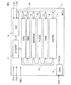
《フラッシュメモリ》
図1には前記フラッシュメモリ6の一例が示される。フラッシュメモリ6は例えば2個のメモリマット21,22を有する。各々のメモリマット21,22はウェル領域にマトリクス配置された複数の不揮発性メモリセルを有する。不揮発性メモリセルは例えばソースとドレインの間のチャネル形成領域の上に夫々絶縁膜を介してシリコンナイトライドのような電荷蓄積層とメモリゲートを積層した所謂MONOS構造を有する。同一行に配置された不揮発性メモリセルのメモリゲートは対応するワード線に、同一列に配置された不揮発性メモリセルのドレインは対応するビット線に接続され、不揮発性メモリセルのソースはソース線に接続される。ここでは消去及び書込みは前記ページ単位とされるから、少なくともワード線方向の1ページの範囲ではウェル領域の分離は行われていない。前記ビット線は例えば1ページ分の不揮発性メモリセルの数分存在する。各ページの記憶領域はページデータ領域(PDAT)とページデータステータス領域(PDATS)とから成る。特に制限されないが、ページデータ領域(PDAT)は256バイト、ページデータステータス領域(PDATS)はiビットとされる。
<Flash memory>
FIG. 1 shows an example of the
消去動作では、例えば、2個のメモリマット21,22はマット制御回路(MATCNT)26で生成されるマット選択信号MS1,MS2によって決定される何れか一方のマットのウェル領域には消去電圧として1.5Vのウェル電圧、消去対象ワード線には消去電圧として−8.5Vのメモリゲート電圧、消去非対象ワード線には消去阻止電圧として1.5Vのメモリゲート電圧が供給され、全てのビット線及びソース線は1.5Vにされる。これにより、ウェル領域から消去対象メモリセルのメモリゲート電極へ向かう電界が形成され、消去対象メモリセルは一括して、電荷蓄積領域に捕獲されている電子が酸化膜を通してFNトンネルにてウェル領域に放出され、これによってそれらメモリセルの閾値電圧は低くされる。書き込み動作では、例えば、2個のメモリマット21,22はマット制御回路(MATCNT)26で生成されるマット選択信号MS1,MS2によって決定される何れか一方のマットのウェル領域には書き込み電圧として−10.7Vのウェル電圧、書き込み対象ワード線には書き込み電圧として1.5Vのメモリゲート電圧、書き込み非対象ワード線には書き込み阻止電圧として−10.7Vのメモリゲート電圧が供給される。書込み選択の不揮発性メモリセルに接続するソース線及びビット線には書き込み電圧として−10.7V、書込み非選択の不揮発性メモリセルに接続するソース線及びビット線には書き込み阻止電圧として1.5Vが印加される。書き込み選択の不揮発性メモリセルにはメモリゲート電極からウェル領域へ向かう電界が形成され、当該メモリセルのウェル領域からFNトンネルにて電荷蓄積領域に電子が捕獲され、その閾値電圧が高くされる。消去及び書込み動作などに用いる高電圧はチャージポンプ回路等を備えた電圧発生回路(VPPG)23で生成される。
In the erase operation, for example, the two
前記ワード線はワードドライバ回路24によって選択的に駆動される。何れのワード線を駆動するかはXアドレスデコーダ(XADEC)25によるデコード出力とマット制御回路(MATCNT)26で生成されるマット選択信号MS1,MS2によって決定される。
The word lines are selectively driven by a
メモリマット21,22の内の何れか一方のメモリマットのビット線がセレクタ回路(BLSEL)27を介して選択される。選択されたビット線の内、前記ページデータ領域に対応するものがセンスアンプ回路(SAA)28とページデータ書き込みラッチ(PDLAT)29に接続され、前記ページデータステータス領域に対応するものがページデータステータス書込みラッチ(PDSLAT)30に接続される。ページデータ書き込みラッチ29の各ビットはデータ線32に接続され、また、データ線32はセンスアンプ回路28の対応入出力ノードがビット対応で接続される。前記データバス13はYスイッチ回路(YSW)33で選択されたバイト単位で前記データ線32に接続可能にされる。Yスイッチ回路33によるバイト単位の選択動作はYアドレスデコーダ(YADEC)35のデコード出力によって制御される。ページデータステータス書込みラッチ30にはマット制御回路26から書込み用のページデータステータスが供給される。前記セレクタ回路27の選択動作は前記マット制御回路26から出力されるマット選択信号MS3,MS4によって制御される。マット制御回路26の動作形態は2ビットのマット制御信号MC1,MC2と、メモリマット21,22のアクセス対象ページから読み込んだページデータステータスとによって決定される。その動作形態の詳細は後述する。
A bit line of one of the
アドレス制御回路(ACNT)37はホストから出力されるアドレス信号ADRSを入力し、それに応じて、前記Xアドレスデコーダ25に供給されるXアドレス信号XADR、Yアドレスデコーダ35に供給されるYアドレス信号YADRS、及び前記マット制御信号MC1,MC2を出力する。アドレス信号ADRSの上位側がXアドレス信号XADR、下位側がYアドレス信号YADRSとされる。
The address control circuit (ACNT) 37 receives an address signal ADRS output from the host, and accordingly, an X address signal XADR supplied to the
内部タイミング制御回路(TCNT)38はアドレス及びコントロールバス14から供給される制御信号の組み合わせ等によって指示されるアクセスコマンドを解読し、その結果に従って、消去動作、書込み動作、又は読出し動作の内部タイミングを生成して、その動作を制御する。前記制御信号は例えばライトイネーブル信号WE、出力イネーブル信号OE、メモリイネーブル信号ME等である。
An internal timing control circuit (TCNT) 38 decodes an access command instructed by a combination of an address and a control signal supplied from the
図4にはフラッシュメモリ6のアドレスマップが例示される。アドレスは16進数で示されている。フラッシュメモリの論理アドレスは0x0000〜0xFFFFの64Kバイトとされる。0x0000〜0x7FFFにはプログラム格納領域が割り当てられる。0x8000〜0xFFFFはデータ格納領域に割り当てられるが、0x8000〜0xBFFFはアクセス不可能領域になっている。便宜上、データ格納領域をバイトアクセス領域、プログラム格納領域をページアクセス領域とも称する。メモリマット21には奇数ページが割り当てられ、メモリマット22には偶数ページが割り当てられる。ページデータステータス領域(PDATS)はデータ格納領域に対して有意とされ、プログラム格納領域に対しては無意味とされる。
FIG. 4 illustrates an address map of the
図5にはマット制御信号MC1,MC2の意義が例示される。アドレス制御回路37は入力されるアドレス信号ADSRSがバイトアクセス領域を指定しているかページアクセス領域を指定しているかを判別する。ページアクセス領域が指定されているときは、そのアドレス信号ADSRSが奇数ページのアドレスであればマット制御信号をMC1,MC2=01とする。これに応答してマット制御回路26はMS1を活性化してワードドライバ回路24に対しメモリマット21のワード線を駆動可能とし、BS1を活性化してセレクタ回路27にデータ線32のメモリマット21への接続を選択させる。これにより、メモリマット21のアクセスが可能になる。一方、ページアクセス領域が指定されているときは、そのアドレス信号ADSRSが偶数ページのアドレスであればマット制御信号をMC1,MC2=10とする。これに応答してマット制御回路26はMS2を活性化してワードドライバ回路24に対しメモリマット22のワード線を駆動可能とし、BS2を活性化してセレクタ回路27にデータ線32のメモリマット22への接続を選択させる。これにより、メモリマット22のアクセスが可能になる。
FIG. 5 illustrates the significance of the mat control signals MC1 and MC2. The
バイトアクセス領域が指定されているとき、テストモードでなければマット制御信号MC1,MC2=00、テストモードであればマット制御信号MC1,MC2=11とする。テスト動作は例えば図示を省略するコントロールレジスタのテストモードビットがセットされることによって指定される。マット制御信号がMC1,MC2=00のとき、マット制御回路26は信号MS1,MS2を共に活性化し、双方のメモリマット21,22においてページ選択動作を可能にする。マット制御回路26は双方のメモリマットから読み出されたページデータステータスを入力し、そのページデータステータスの状態に応じてセレクタ回路27にデータ線32をメモリマット21又は22の何れか一方に接続させる。読み出し動作ではセレクタ回路27で導通が選択された一方のメモリマットから読み出されたページデータがセンスアンプ回路28でセンス増幅され、Yアドレス信号YADRSに従ってYスイッチ回路33で選択されたバイトデータがデータバス13に出力される。消去及び書込み動作ではセレクタ回路27で導通が選択された一方のメモリマットから読み出されたページデータがページデータラッチ回路29にラッチされ、ラッチされたページデータは、バス13から入力されてYスイッチ回路33で選択されて供給された書込みバイトデータとマージされる。セレクタ回路27を介してデータ線32に導通された一方のメモリマットからマット制御回路26に読み出されたページデータステータスは最も最近更新したことが分かるよう更新され、更新されたページデータステータスがページデータステータスラッチ回路30にロードされる。ページデータラッチ回路29が保持する更新されたページデータと、ページデータステータスラッチ回路30が保持する更新されたページデータステータスは、前記とは反対側のメモリマットに書込まれる。
When the byte access area is specified, the mat control signals MC1, MC2 = 00 are set if the test mode is not set, and the mat control signals MC1, MC2 = 11 are set if the test mode is set. The test operation is specified by setting a test mode bit of a control register (not shown), for example. When the mat control signals are MC1, MC2 = 00, the
テストモードにおいてマット制御信号がMC1,MC2=11のときは、セレクタ回路27の選択形態がページデータステータスによらずに、図示を省略するコントロールレジスタの制御ビットの値に応じて可変可能とされる。したがて、セレクタ回路27による選択形態を、制御信号MC1,MC2=00の時と逆にすることが可能であり、バックアップされたデータを外部に読み出して検証したりすることが可能になる。
When the mat control signal is MC1, MC2 = 11 in the test mode, the selection form of the
図6にはページデータステータスの具体例が示される。ページデータステータスはPDS0〜PDS3の4ビットから成り、PDS0、PDS1は優先順位を示す優先度データとされ、PDS2,PDS3はエラー判定ビットとされる。優先度データPDS0、PDS1は00,01,10,11,00の順に更新され、更新される順に優先度が高くされる。バイトアクセスにおいて双方のメモリマット21,22で選択される一方のメモリマットの選択ページが保有する優先度データPDS0、PDS1が00、他方のメモリマットの選択ページが保有する優先度データPDS0、PDS1が11のときは、00の優先度データの方が優先度が高い。エラー判定ビットPD2,PD3は消去及び書込み動作途中で電源遮断があったかを検出するのに用いる。ページの書換え時に電源遮断によってデータ破壊があると、複数ビットのエラー判定ビットPDS2,PDS3は共に論理値1又は0に揃うことになると考えられるからである。
FIG. 6 shows a specific example of the page data status. The page data status is composed of 4 bits PDS0 to PDS3, PDS0 and PDS1 are priority data indicating priority, and PDS2 and PDS3 are error determination bits. The priority data PDS0 and PDS1 are updated in the order of 00, 01, 10, 1 1 and 00, and the priority is increased in the order of update. In byte access, priority data PDS0 and PDS1 held by the selected page of one memory mat selected by both
図7にはページデータステータスの状態に応じたマット制御回路26による制御形態の概略が例示される。バイトアクセスにおいてメモリマット21,22で選択される一方のメモリマットの選択ページが保有するエラー判定ビットPDS2、PDS3と、他方のメモリマットの選択ページが保有するエラー判定ビットPDS2、PDS3とから、双方のメモリマットから読み出したページデータの有効性を判定する。PDS2とPDS3が同一論理値であれば無効と判定する。共に無効なときは、読み出すべき有効なデータもなければ、書換えられるべき有効なデータもないので、エラー処理を行なう。例えばマット制御回路26はCPUに向けてエラーコード若しくはデータエラーの割り込みを出力する。一方が有効であれば、当該一方のページデータを読出し対象とし、書き換え時には当該無効なページを書込み対象とするように信号BS1,BS2によってセレクタ回路27を制御する。上記書換え時にマット制御回路26は、有効とされたページの優先度データPDS0、PDS1とエラー判定ビットPDS2、PDS3を夫々1段階更新した新たな優先順位データとパリティーとをラッチ回路30にラッチし、これをページデータと一緒にして書き換えデータとする。双方共に有効な時は、優先度データPDS0、PDS1を参照してページデータの優先度を判定する。双方のメモリマットから読み出されたページデータに対しては優先度の高い方をデータ線32に導通させるように信号BS1,BS2によってセレクタ回路27を制御して選択する。書込み時には優先度の低い方のページデータを格納するメモリマットのページを書込み対象とするように信号BS1,BS2によってセレクタ回路27を制御する。上記書込み時にマット制御回路26は、優先順位が高い方のページの優先度データPDS0、PDS1とエラー判定ビットPDS2、PDS3を夫々1段階更新した新たな優先順位データとパリティーとをラッチ回路30にラッチし、これをページデータと一緒にして書き換えデータとする。
FIG. 7 illustrates an outline of a control form by the
これにより、バイトアクセス領域に対する書込み動作において、一のメモリマットの中で選択された最も最近書換えられた有効ページには書換え対象バイト以外のデータがそのまま保存され、他のメモリマットの中で選択されたページには書換え対象バイトが更新されたページデータが新たに書き込まれることになる。したがって、一のメモリマットの中で選択されたページは他のメモリマットの中で選択されて書換えられたページに対して書換え前の実質的なバックアップデータを保有することになる。メモリマットに対する消去及び書込み動作中に電源が遮断されても、今回書き込み非対象とされたデータは消失せずに、反対側のメモリマットの対応ページに残っている。バックアップのために別の領域にデータを転送するための別のアクセス動作を追加することを要しない。 As a result, in a write operation to the byte access area, data other than the byte to be rewritten is stored as it is in the most recently rewritten valid page selected in one memory mat, and selected in another memory mat. The page data in which the rewrite target byte is updated is newly written in the new page. Therefore, a page selected in one memory mat holds substantial backup data before rewriting with respect to a page selected and rewritten in another memory mat. Even if the power is cut off during the erase and write operations on the memory mat, the data that is not targeted for writing this time is not lost and remains on the corresponding page of the memory mat on the opposite side. It is not necessary to add another access operation for transferring data to another area for backup.
図8にはページアクセス領域に対するバイト読出し動作におけるデータの流れが示される。MC1,MC2=01又は10とされる。マット制御回路26はMC1,MC2の値に応じてワードドライバ回路24及びセレクタ回路27を選択制御する。MC1,MC2=01のページアクセスの場合にはXアドレス信号XADRSに従ってメモリマット21のワード線が駆動されてページが選択され、選択されたページデータがセンスアンプ回路28によってセンス増幅され、センスアンプ回路28に保持されたページデータに対してYスイッチ回路33がYアドレス信号YADRSに基づいてバイトデータを選択し、選択されたバイトデータがデータバス13に出力される。MC1,MC2=10のページアクセスの場合にはメモリマット22のワード線が駆動されて、同様のバイト読出しが行われる。
FIG. 8 shows the data flow in the byte read operation for the page access area. MC1, MC2 = 01 or 10. The
図9にはバイトアクセス領域に対するバイト読出し動作におけるデータの流れが示される。MC1,MC2=00とされる。Xアドレスデコーダ25はXアドレス信号XADRSにしたがってワード線選択信号を形成する。マット制御回路26はワードドライバ回路24を介して双方のメモリマット21,22で前記ワード線選択信号に従ってワード線を駆動し、双方のメモリマット21,22で選択されたページのページデータステータスを取得する。マット制御回路26は双方のページのページデータステータスからページの有効性を判定し、図7で説明した制御形態に従い、例えば一方のみ有効であれば当該有効ページのページデータをセレクタ回路27で選択する。双方のページが有効であるときは優先順位の高い方のページのページデータをセレクタ回路27で選択する。双方無効であればエラー処理を通知する。セレクタ回路27で選択されたページデータはセンスアンプ回路28によってセンス増幅される。センスアンプ回路28に保持されたページデータに対してYスイッチ回路33がYアドレス信号YADRSに基づいてバイトデータを選択し、選択されたバイトデータがデータバス13に出力される。
FIG. 9 shows the data flow in the byte read operation for the byte access area. MC1, MC2 = 00.
図10にはページアクセス領域に対するページ書込み動作におけるデータの流れが示される。Yスイッチ回路33がYアドレス信号YADRSに基づいてバイト単位でデータ線を選択する。Yアドレス信号YADRSの順位インクリメントに同期しながら、データバス13から書込みバイトデータが順次入力されると、バイト単位の書き込みデータが順次下位側より上位側に向けて書込みデータラッチ回路29にラッチされる。MC1,MC2=01又は10とされ、マット制御回路26は、MC1,MC2の値に応じてデータ線をメモリマット21又は22に接続し、MC1,MC2の値に応じてワードドライバ回路24を選択駆動する。これにより、MC1,MC2=01のページアクセスの場合にはメモリマット21で選択されたページに1ページのデータが書き込まれる。この例では書込みデータはプログラムとされる。
FIG. 10 shows the flow of data in the page write operation for the page access area. The
図11及び図12にはバイトアクセス領域に対するバイト書換え動作におけるデータの流れが示される。特に図11は書換え対象ページデータを書き込みバイトデータでマージするためのデータ読出しにおけるデータの流れを示す。図12はマージされたページデータによる書込み動作のデータの流れを示す。MC1,MC2=00とされる。図11においてXアドレスデコーダ25はXアドレス信号XADRSにしたがってワード線選択信号を形成する。マット制御回路26はワードドライバ回路24を介して双方のメモリマット21,22で前記ワード線選択信号に従ってワード線を駆動し、双方のメモリマット21,22で選択されたページのページデータステータスを取得する。マット制御回路26は双方のページのページデータステータスからページの有効性を判定し、図7で説明した制御形態に従い、例えば一方のみ有効であれば当該有効ページのページデータをセレクタ回路27で選択する。双方のページが有効であるときは優先順位の高い方のページのページデータをセレクタ回路27で選択する。双方無効であればエラー処理を通知する。セレクタ回路27で選択されたページデータはセンスアンプ回路28によってセンス増幅される。センスアンプ回路28に保持されたページデータはページデータ書き込みラッチ回路29に内部転送される。ページデータ書き込みラッチ回路29には、データバス13から入力された書き込みバイトデータがYスイッチ回路33を介して供給される。供給されるバイト位置はYアドレス信号YADRSによってYスイッチ回路33が選択する。これにより、ページデータ書込みラッチ回路29上において、優先順位の高い方のページデータが書込みバイトデータによってマージされる。ページデータスタータス書込みラッチ回路30には前記マージされたページデータと一緒に書き込まれる新たなページデータステータスがマット制御回路26によって用意される。用意されるページデータステータは、ページデータ書き込みラッチ回路29にラッチされたページデータの優先順位よりも高い優先順を有し、また其れとは異なるパリティーを有する。
11 and 12 show the data flow in the byte rewrite operation for the byte access area. In particular, FIG. 11 shows a data flow in data reading for merging page data to be rewritten with write byte data. FIG. 12 shows the data flow of a write operation using merged page data. MC1, MC2 = 00. In FIG. 11, the
書込み用のページデータが用意されると、今度は図12のデータ経路で書込みページに対する消去処理と、書込み処理が行われる。即ち、マット制御回路26は前記ページデータ書き込みラッチ回路29にロードしたデータのページとは反対側のメモリマットの対応ページを消去及び書込み処理の対象とする。その規則は図7で説明した通りであり、優先順位の低い方のページ又は無効なページとされる。先ず、その消去及び書込み対象ページに対してページ一括で消去処理が行なわれる。次に、当該ページに対してページデータ書き込みラッチ回路29とページデータステータ書込みラッチ回路30に保持されているデータがセレクタ回路27を介して対応するメモリマットの前記消去及び書込み対象ページに供給されて書き込まれる。消去及び書込み処理のタイミング制御はタイミング制御回路38が行う。
When the page data for writing is prepared, the erasing process and the writing process for the write page are performed in the data path of FIG. That is, the
図11及び図12に示されるバイトアクセス領域に対するバイト書換え動作より明らかなように、双方のメモリマット21,22で選択されたページが共に有効であるとき、双方のページのなかで優先順位の高い方の有効ページには書換え対象バイト以外のデータがそのまま保存され、優先順位の低い方のページには書換え対象バイトが更新されたページデータが新たに書き込まれることになる。したがって、一のメモリマットの中で選択されたページは他のメモリマットの中で選択されて書換えられたページに対して書換え前の実質的なバックアップデータを保有することになる。メモリマットに対する消去及び書込み動作中に電源が遮断されても、今回書き込み非対象とされたデータは消失せずに、反対側のメモリマットの対応ページに残っている。双方のメモリマットで選択された一方のページが無効であるときは、有効ページには書換え対象バイト以外のデータがそのまま保存され、当初無効とされたページには書換え対象バイトが更新されたページデータが新たに書き込まれることになる。したがって、当初有効とされた一のページは書き込み対象とされた当初無効なページに対して書換え前の実質的なバックアップデータを保有することになる。メモリマットに対する消去及び書込み動作中に電源が遮断されても、今回書き込み非対象とされたデータは消失せずに、当初有効とされたページに残っている。したがって、バックアップのために別の領域にデータを転送するための別のアクセス動作を追加することを要しないから、ICカード用マイコン1においてフラッシュメモリ6に対するバイト書き換えを伴うデータ処理の高速化に資することができる。当然、フラッシュメモリ6の不揮発性メモリセルはバイト単位のウェル領域分離を行うことを要しないから、フラッシュメモリ6の占有面積を大凡40%縮小することができる。データ領域(バイトアクセス領域)がプログラム領域(ページアクセス領域)の大凡半分とすると、データ領域の実質記憶容量はプログラム領域の記憶容量の大凡半分になるが、全体的には単位記憶容量に対する占有面積は小さくなる。
As is clear from the byte rewriting operation for the byte access area shown in FIGS. 11 and 12, when both the pages selected in both
特に図示はしないが、テストモードにおいてMC1,MC2=11の場合には、バイトアクセス領域に対するバイトアクセス動作において、選択された双方のページが有効なとき、読出し選択されるページの選択はページデータステータスに依存されず、図示を省略するコントロールレジスタの所定の制御ビットの値に依存する。従って、テストモードにおいて、コントロールレジスタの所定の制御ビットの値を第1の値にすればMC1,MC2=00の場合と同様の動作を行うことができ、コントロールレジスタの所定の制御ビットの値を第2の値にすれば、バックアップ側のページデータを読み出して、バックアップが正常に行われているか否かを検証したりすることができる。 Although not shown in particular, in the case of MC1, MC2 = 11 in the test mode, in the byte access operation for the byte access area, when both selected pages are valid, the selection of the page selected for reading is the page data status. It depends on the value of a predetermined control bit of a control register (not shown). Therefore, in the test mode, if the value of the predetermined control bit in the control register is set to the first value, the same operation as in the case of MC1, MC2 = 00 can be performed, and the value of the predetermined control bit in the control register can be changed. With the second value, page data on the backup side can be read to verify whether backup has been performed normally.
図13にはフラッシュメモリ6のアドレスマップの別の例が示される。アドレスは16進数で示されている。フラッシュメモリの論理アドレスは0x0000〜0xFFFFの64Kバイトとされ、0x0000〜0x7FFFにはプログラム格納領域が割り当てられ、0x8000〜0xFFFFはデータ格納領域に割り当てられている点は図4と同じである。相違点は、バイトアクセス領域におけるアクセス不可能領域のマッピングである。図4では、その下位側半分の0x8000〜0xBFFFのリニアな空間をアクセス不可能領域としたが、図13では、ページデータ領域とページサイズのアクセス不能領域とを交互に配置した。メモリマット21には奇数ページが割り当てられ、メモリマット22には偶数ページが割り当てられる点が図13と同じである。図14には図13のアドレスマップに対応するマット制御信号MC1,MC2の意義が例示される。図5とはアクセスアドレス範囲が相違する。
FIG. 13 shows another example of the address map of the
図4及び図5のように、前記バイトアクセス領域をアクセス不可能な領域とアクセス可能な領域とに2分割する場合は、Xアドレス信号XADRSをデコードするデコーダ25のデコード論理は、ページアクセスだけのデコード論理に対して1ビット少ないアドレス情報に対するデコード論理を持つことが必要になり、これに応じてアドレス制御回路37はCPUからのアクセスアドレス信号ADRSからXアドレス信号XADRSを切り出すときその上位側アドレスビットの1ビットを削除することが必要になる。図13及び図14のように、バイトアクセス領域にページデータ領域とアクセス不能なページ領域を交互に配置する場合は、Xアドレス信号XADRSをデコードするデコーダ25のデコード論理は、ページアクセスだけのデコード論理と同じであってよく、アドレス制御回路37もCPUからのアクセスアドレスADRSの上位側からXアドレス信号XADRSを単に切り出して出力すればよい。この意味では、図13及び図14のアドレスマッピングを採用することで、アドレス制御回路37にデータ格納領域を設定するレジスタを設け、ソフトにてレジスタの値を書換えデータ格納領域を設定できる。
As shown in FIGS. 4 and 5, when the byte access area is divided into an inaccessible area and an accessible area, the decoding logic of the
以上本発明者によってなされた発明を実施形態に基づいて具体的に説明したが、本発明はそれに限定されるものではなく、その要旨を逸脱しない範囲において種々変更可能であることは言うまでもない。 Although the invention made by the present inventor has been specifically described based on the embodiments, it is needless to say that the present invention is not limited thereto and can be variously modified without departing from the gist thereof.
例えば、ページサイズは256バイトに限定されず、またバイトアクセスは8ビットアクセスに限定されず、適宜変更可能である。メモリマットの数は2個に限定されず4個又は8個等であってもよい。一部のメモリマットをバイトアクセス制御に割り当て、残りのメモリマットをページアクセス制御に割り当てるようにしても良い。不揮発性メモリセルはMONOS構造に限定されず、フローティングゲート構造であっても良い。また、スプリットゲートゲート構造の不揮発性メモリセルを採用することも可能である。メモリマットのアレイ構成はAND型に限定されず、NAND、NOR等のその他適宜のアレイ構成を採用することが可能である。エラー判定ビットや優先度データのビット数やビット配置は適宜変更可能である。エラー判定ビットとして01と10を交互に用いたが、01又は10のように、相互に論理値の異なる1種類のビット配列をエラー判定ビットとして採用してもよい。また、フラッシュメモリの外部インタフェースビット数はバイトに限定されない。2バイト又は4バイト等の単位であってもよい。バイトアクセス制御に際してバイトデータを切り出せばよい。不揮発性メモリに対する外部からのアクセス制御にはデータバスから供給されるコマンドを用いるようにしても良い。また、アドレス制御回路はフラッシュメモリ内のメモリ制御回路の一部の機能として備える場合に限定されない。例えば、マイクロコンピュータ内部のMMU(メモリ・マネージメント・ユニット)、バスステートコントローラ、又はメモリコントローラがその機能を備えてもよい。 For example, the page size is not limited to 256 bytes, and byte access is not limited to 8-bit access, and can be changed as appropriate. The number of memory mats is not limited to two and may be four or eight. Some memory mats may be assigned to byte access control, and the remaining memory mats may be assigned to page access control. The nonvolatile memory cell is not limited to the MONOS structure and may have a floating gate structure. It is also possible to employ a non-volatile memory cell having a split gate gate structure. The array configuration of the memory mat is not limited to the AND type, and other appropriate array configurations such as NAND and NOR can be adopted. The number of bits and the bit arrangement of error determination bits and priority data can be changed as appropriate. Although 01 and 10 are alternately used as the error determination bits, one type of bit arrangement having different logical values, such as 01 or 10, may be adopted as the error determination bits. Further, the number of external interface bits of the flash memory is not limited to bytes. A unit of 2 bytes or 4 bytes may be used. Byte data may be cut out for byte access control. A command supplied from the data bus may be used for external access control to the nonvolatile memory. The address control circuit is not limited to the case where it is provided as a partial function of the memory control circuit in the flash memory. For example, an MMU (memory management unit), a bus state controller, or a memory controller inside the microcomputer may have the function.
本発明が適用されるマイクロコンピュータはICカード用マイクロコンピュータに限定されない。汎用マイクロコンピュータに適用してもよい。その場合には、不揮発性メモリ領域は全てデータ格納領域、即バイトアクセス領域にしても良い。その場合には、単位記憶容量に対するフラッシュメモリの占有面積は小さくならないが、2個のメモリマットに交互に書込む制御形態が採用されるが故に、書換え可能回数の上限を見掛け上約2倍にすることができ、書換え可能な不揮発性データ格納領域の寿命を延ばすことができる。この意味において、本発明はプログラム格納領域を設定しない不揮発性メモリを持つ半導体処理装置にも適用可能である。半導体処理装置はマイクロコンピュータに限定されず、コプロセッサやアクセラレータ等、データ処理を行なう半導体集積回路に広く適用することができる。 The microcomputer to which the present invention is applied is not limited to the IC card microcomputer. You may apply to a general purpose microcomputer. In that case, all the nonvolatile memory areas may be data storage areas and immediate byte access areas. In this case, the area occupied by the flash memory with respect to the unit storage capacity is not reduced, but the control mode of alternately writing to the two memory mats is adopted, so that the upper limit of the number of rewritable times is apparently doubled. The life of the rewritable nonvolatile data storage area can be extended. In this sense, the present invention is also applicable to a semiconductor processing apparatus having a nonvolatile memory in which no program storage area is set. The semiconductor processing apparatus is not limited to a microcomputer, and can be widely applied to semiconductor integrated circuits that perform data processing, such as a coprocessor and an accelerator.
1 マイクロコンピュータ
2 CPU
6 フラッシュメモリ
13 データバス
14 アドレス及びコントロールバス
21,22 メモリマット
PDAT ページデータ領域
PDATS ページデータステータス領域
PDS0、PDS1 優先度データ
PDS2,PDS3 エラー判定ビット
24 ワードドライバ回路
25 Xアドレスデコーダ(XADEC)
26 マット制御回路(MATCNT)
MS1,MS2 マット選択信号
27 セレクタ回路(BLSEL)
28 センスアンプ回路(SAA)28
29 ページデータ書き込みラッチ(PDLAT)
30 ページデータステータス書込みラッチ(PDSLAT)
32 データ線32
33 Yスイッチ回路
35 Yアドレスデコーダ(YADEC)
37 アドレス制御回路(ACNT)
ADRS アドレス信号
XADR Xアドレス信号
YADRS Yアドレス信号
MC1,MC2 マット制御信号
38 内部タイミング制御回路(TCNT)
1
6
26 Mat control circuit (MATCNT)
MS1, MS2
28 sense amplifier circuit (SAA) 28
29 Page data write latch (PDLAT)
30 Page data status write latch (PDSLAT)
32
33 Y switch circuit 35 Y address decoder (YADEC)
37 Address control circuit (ACNT)
ADRS address signal XADR X address signal YADRS Y address signal MC1, MC2 Matt control signal 38 Internal timing control circuit (TCNT)
Claims (21)
前記不揮発性メモリは、ページ単位で書換え動作が可能にされる複数のメモリマットと、前記データ処理ユニットからのアクセス指示に応答して前記メモリマットに対するメモリ動作を制御するメモリ制御回路とを有し、
前記メモリ制御回路はメモリマットの所定のアドレス領域に対するアクセスに応答してバイトアクセス制御を行い、その他のアドレス領域に対するアクセスに応答してページアクセス制御を行い、
前記メモリ制御回路はバイトアクセス制御において複数のメモリマットの各々のページから当該ページの管理情報を読み出し、読み出した管理情報から有効ページの中で最も最近書換えられたページを判定し、データ書き換えでは前記判定したページから読出したデータをバイト単位の書込みデータでマージし、マージしたデータを他のメモリマットの中で選択した対応ページに書き込み、読出しでは前記判定されたページから読出しを行う半導体処理装置。 A rewritable nonvolatile memory, and a data processing unit capable of accessing the nonvolatile memory,
The nonvolatile memory includes a plurality of memory mats that can be rewritten on a page basis, and a memory control circuit that controls memory operations on the memory mat in response to an access instruction from the data processing unit. ,
The memory control circuit performs byte access control in response to access to a predetermined address area of the memory mat, performs page access control in response to access to other address areas,
The memory control circuit reads the management information of the page from each page of a plurality of memory mats in byte access control, determines the most recently rewritten page among the valid pages from the read management information. A semiconductor processing apparatus that merges data read from a determined page with write data in units of bytes, writes the merged data to a corresponding page selected in another memory mat, and reads from the determined page in reading.
前記メモリ制御回路は前記選択されたページの有効性を当該ページが保有する前記エラー判定ビットによって判定する請求項1記載の半導体処理装置。 The management information includes a plurality of error determination bits for indicating whether or not the data held by the page is destroyed,
The semiconductor processing apparatus according to claim 1, wherein the memory control circuit determines the validity of the selected page by the error determination bit held by the page.
前記制御回路は、優先度の高い優先度データに対応するページほど最近書換えられたページであると判定する請求項4記載の半導体処理装置。 The management information has a plurality of bits of priority data for indicating the priority of data held by the page,
The semiconductor processing apparatus according to claim 4, wherein the control circuit determines that a page corresponding to priority data having a higher priority is a page that has been recently rewritten.
前記ページアクセス制御の対象とされる前記その他のアドレス領域はプログラム格納領域とされる請求項1記載の半導体処理装置。 The predetermined address area targeted for the byte access control is a data storage area,
2. The semiconductor processing apparatus according to claim 1, wherein the other address area subject to the page access control is a program storage area.
前記ページアクセス制御の対象とされる前記その他のアドレス領域は第2のデータ格納領域とされる請求項1記載の半導体処理装置。 The predetermined address area targeted for the byte access control is a first data storage area,
2. The semiconductor processing apparatus according to claim 1, wherein the other address area subject to the page access control is a second data storage area.
前記アドレス制御部は、前記データ処理ユニットから供給されるアクセスアドレス信号を入力し、入力したアクセスアドレス信号に対してページを選択するページ選択アドレスとページ内のバイトを選択するバイト選択アドレスと、2ビットのマット選択制御信号とを生成し、
前記アドレス制御部は、前記ページアクセス制御を指定する前記アクセスアドレス信号に対しては2個のメモリマットに共通のページアドレスを生成すると共に前記アクセスアドレス信号の所定の1ビットの値に応じて前記マット選択制御信号を第1の値又は第2の値とし、前記バイトアクセス制御を指定する前記アクセスアドレス信号対しては2個のメモリマットに共通のページアドレスを生成すると共にその他の制御情報に基づいて前記マット選択制御信号を第3の値又は第4の値とし、
前記メモリ制御回路は、前記マット選択制御信号が第3の値のときは前記最も最近書換えられたと判定されたページから読出しを行う請求項1記載の半導体処理装置。 The memory control circuit has an address control unit;
The address control unit receives an access address signal supplied from the data processing unit, selects a page with respect to the input access address signal, a byte selection address that selects a byte within the page, and 2 Bit mat selection control signal and
The address control unit generates a page address common to two memory mats for the access address signal designating the page access control and according to a predetermined 1-bit value of the access address signal A mat selection control signal is set to a first value or a second value, and for the access address signal designating the byte access control, a page address common to two memory mats is generated and based on other control information The mat selection control signal is set to the third value or the fourth value,
The semiconductor processing apparatus according to claim 1, wherein the memory control circuit reads from the page determined to be most recently rewritten when the mat selection control signal is a third value.
前記不揮発性メモリは、ページ単位で書換え動作が可能にされる複数のメモリマットと、前記データ処理ユニットからのアクセス指示に応答して前記メモリマットに対するバイトアクセス制御が可能なメモリ制御回路とを有し、
前記メモリ制御回路はバイトアクセス制御において複数のメモリマットの各々のページから当該ページの管理情報を読み出し、読み出した管理情報から有効ページの中で最も最近書換えられたページを判定し、データ書き換えでは前記判定したページから読出したデータをバイト単位の書込みデータでマージし、マージしたデータを他のメモリマットの中で選択した対応ページに書き込み、読出しでは前記判定されたページから読出しを行う半導体処理装置。 A rewritable nonvolatile memory, and a data processing unit capable of accessing the nonvolatile memory,
The nonvolatile memory includes a plurality of memory mats that can be rewritten on a page basis, and a memory control circuit that can perform byte access control on the memory mat in response to an access instruction from the data processing unit. And
The memory control circuit reads the management information of the page from each page of a plurality of memory mats in byte access control, determines the most recently rewritten page among the valid pages from the read management information. A semiconductor processing apparatus that merges data read from a determined page with write data in units of bytes, writes the merged data to a corresponding page selected in another memory mat, and reads from the determined page in reading.
前記メモリ制御回路は前記選択されたページの有効性を当該ページが保有する前記エラー判定ビットによって判定する請求項14記載の半導体処理装置。 The management information includes a plurality of error determination bits for indicating whether or not the data held by the page is destroyed,
15. The semiconductor processing apparatus according to claim 14, wherein the memory control circuit determines the validity of the selected page by the error determination bit held by the page.
前記制御回路は、優先度の高い優先度データに対応するページほど最近書換えられたページであると判定する請求項17記載の半導体処理装置。 The management information has a plurality of bits of priority data for indicating the priority of data held by the page,
18. The semiconductor processing apparatus according to claim 17, wherein the control circuit determines that a page corresponding to priority data having a higher priority is a page that has been recently rewritten.
前記不揮発性メモリは、ページ単位で書換え動作が可能にされる複数のメモリマットと、外部からのアクセス指示に応答して前記メモリマットに対するバイトアクセス制御を行うメモリ制御回路とを有し、
前記メモリ制御回路はバイトアクセス制御において複数のメモリマットの各々のページから当該ページの管理情報を読み出し、読み出した管理情報から有効ページの中で最も最近書換えられたページを判定し、データ書き換えでは前記判定したページから読出したデータをバイト単位の書込みデータでマージし、マージしたデータを他のメモリマットの中で選択した対応ページに書き込み、読出しでは前記判定されたページから読出しを行う半導体集積回路。 Having rewritable nonvolatile memory,
The nonvolatile memory includes a plurality of memory mats that can be rewritten in units of pages, and a memory control circuit that performs byte access control on the memory mat in response to an access instruction from the outside.
The memory control circuit reads the management information of the page from each page of a plurality of memory mats in byte access control, determines the most recently rewritten page among the valid pages from the read management information. A semiconductor integrated circuit that merges data read from a determined page with write data in byte units, writes the merged data to a corresponding page selected in another memory mat, and reads from the determined page in reading.
前記不揮発性メモリは、ページ単位で書換え動作が可能にされる複数のメモリマットと、外部からのアクセス指示に応答して前記メモリマットに対するバイトアクセス制御を行うメモリ制御回路とを有し、
前記メモリ制御回路はバイトアクセス制御において複数のメモリマットを動作させ、データ書き換えでは一のメモリマットの中で選択されたページから読出したデータを書込みバイトデータでマージし、マージしたデータを他のメモリマットの中で選択された対応ページに書き込み、読出しでは複数のメモリマットの各々で選択されたページのうち有効なページであって最も最近書換えられたページから読出しを行う半導体集積回路。 Having rewritable nonvolatile memory,
The nonvolatile memory includes a plurality of memory mats that can be rewritten in units of pages, and a memory control circuit that performs byte access control on the memory mat in response to an access instruction from the outside.
The memory control circuit operates a plurality of memory mats in byte access control, and in data rewriting, data read from a page selected in one memory mat is merged with write byte data, and the merged data is transferred to another memory. A semiconductor integrated circuit for writing to a corresponding page selected in a mat and reading from a page that is an effective page among the pages selected in each of a plurality of memory mats and has been most recently rewritten.
Priority Applications (2)
| Application Number | Priority Date | Filing Date | Title |
|---|---|---|---|
| JP2005331334A JP2007140733A (en) | 2005-11-16 | 2005-11-16 | Semiconductor processor and semiconductor integrated circuit |
| US11/599,264 US20070113001A1 (en) | 2005-11-16 | 2006-11-15 | Semiconductor processor and semiconductor integrated circuit |
Applications Claiming Priority (1)
| Application Number | Priority Date | Filing Date | Title |
|---|---|---|---|
| JP2005331334A JP2007140733A (en) | 2005-11-16 | 2005-11-16 | Semiconductor processor and semiconductor integrated circuit |
Publications (1)
| Publication Number | Publication Date |
|---|---|
| JP2007140733A true JP2007140733A (en) | 2007-06-07 |
Family
ID=38042277
Family Applications (1)
| Application Number | Title | Priority Date | Filing Date |
|---|---|---|---|
| JP2005331334A Withdrawn JP2007140733A (en) | 2005-11-16 | 2005-11-16 | Semiconductor processor and semiconductor integrated circuit |
Country Status (2)
| Country | Link |
|---|---|
| US (1) | US20070113001A1 (en) |
| JP (1) | JP2007140733A (en) |
Cited By (3)
| Publication number | Priority date | Publication date | Assignee | Title |
|---|---|---|---|---|
| US8332579B2 (en) | 2010-05-31 | 2012-12-11 | Kabushiki Kaisha Toshiba | Data storage apparatus and method of writing data |
| JP2014222528A (en) * | 2014-07-08 | 2014-11-27 | 株式会社東芝 | Memory system and method of controlling nonvolatile memory |
| US9053007B2 (en) | 2011-03-28 | 2015-06-09 | Kabushiki Kaisha Toshiba | Memory system, controller, and method for controlling memory system |
Families Citing this family (7)
| Publication number | Priority date | Publication date | Assignee | Title |
|---|---|---|---|---|
| US8041883B2 (en) * | 2007-05-09 | 2011-10-18 | Stmicroelectronics S.R.L. | Restoring storage devices based on flash memories and related circuit, system, and method |
| US7991942B2 (en) * | 2007-05-09 | 2011-08-02 | Stmicroelectronics S.R.L. | Memory block compaction method, circuit, and system in storage devices based on flash memories |
| US7882301B2 (en) * | 2007-05-09 | 2011-02-01 | Stmicroelectronics S.R.L. | Wear leveling in storage devices based on flash memories and related circuit, system, and method |
| US20080282024A1 (en) * | 2007-05-09 | 2008-11-13 | Sudeep Biswas | Management of erase operations in storage devices based on flash memories |
| JP4800415B2 (en) * | 2009-08-17 | 2011-10-26 | 富士通株式会社 | Relay device and MAC address search method |
| US10937499B2 (en) * | 2019-04-12 | 2021-03-02 | Micron Technology, Inc. | Content addressable memory systems with content addressable memory buffers |
| US20220269645A1 (en) * | 2019-08-13 | 2022-08-25 | Neuroblade Ltd. | Memory mat as a register file |
Family Cites Families (6)
| Publication number | Priority date | Publication date | Assignee | Title |
|---|---|---|---|---|
| JPH04263386A (en) * | 1991-02-18 | 1992-09-18 | Fuji Photo Film Co Ltd | Ic memory card |
| TW231343B (en) * | 1992-03-17 | 1994-10-01 | Hitachi Seisakusyo Kk | |
| US5590306A (en) * | 1992-09-08 | 1996-12-31 | Fuji Photo Film Co., Ltd. | Memory card management system for writing data with usage and recording codes made significant |
| US5696917A (en) * | 1994-06-03 | 1997-12-09 | Intel Corporation | Method and apparatus for performing burst read operations in an asynchronous nonvolatile memory |
| GB9801373D0 (en) * | 1998-01-22 | 1998-03-18 | Memory Corp Plc | Memory system |
| JP4037605B2 (en) * | 2000-12-04 | 2008-01-23 | 株式会社東芝 | Nonvolatile memory unit controller, memory system having the controller, and nonvolatile memory unit control method |
-
2005
- 2005-11-16 JP JP2005331334A patent/JP2007140733A/en not_active Withdrawn
-
2006
- 2006-11-15 US US11/599,264 patent/US20070113001A1/en not_active Abandoned
Cited By (3)
| Publication number | Priority date | Publication date | Assignee | Title |
|---|---|---|---|---|
| US8332579B2 (en) | 2010-05-31 | 2012-12-11 | Kabushiki Kaisha Toshiba | Data storage apparatus and method of writing data |
| US9053007B2 (en) | 2011-03-28 | 2015-06-09 | Kabushiki Kaisha Toshiba | Memory system, controller, and method for controlling memory system |
| JP2014222528A (en) * | 2014-07-08 | 2014-11-27 | 株式会社東芝 | Memory system and method of controlling nonvolatile memory |
Also Published As
| Publication number | Publication date |
|---|---|
| US20070113001A1 (en) | 2007-05-17 |
Similar Documents
| Publication | Publication Date | Title |
|---|---|---|
| JP2007140733A (en) | Semiconductor processor and semiconductor integrated circuit | |
| JP4129381B2 (en) | Nonvolatile semiconductor memory device | |
| TWI391936B (en) | Memory device architectures and operation | |
| JP5311784B2 (en) | Semiconductor device | |
| KR100320360B1 (en) | Program memory for remote reprogrammable microcontrollers | |
| US10359944B2 (en) | Memory devices having distributed controller systems | |
| KR100939146B1 (en) | Non-volatile semiconductor memory system and data write method thereof | |
| JP5016841B2 (en) | Nonvolatile semiconductor memory device | |
| JP2008502090A (en) | Memory device with user-configurable density / operation performance | |
| US6922362B2 (en) | Structure for updating a block of memory cells in a flash memory device with erase and program operation reduction | |
| JP4499111B2 (en) | Information setting method for nonvolatile memory device and nonvolatile memory device | |
| KR100837273B1 (en) | Flash memory device | |
| US7310277B2 (en) | Non-volatile semiconductor storage device with specific command enable/disable control signal | |
| JP2008251154A (en) | Nonvolatile semiconductor memory device | |
| JP2006323499A (en) | Semiconductor device | |
| KR100965079B1 (en) | Non volatiel memory device | |
| JP2003006053A (en) | Data processor | |
| JPH0877081A (en) | File memory system | |
| JPH11185485A (en) | Semiconductor storage and data processor | |
| JP4018085B2 (en) | Nonvolatile memory, memory card using the same, information processing apparatus, and software write protection control method for nonvolatile memory | |
| JP2006221677A (en) | Memory card | |
| JP2005085316A (en) | Nonvolatile semiconductor memory | |
| JPH11283379A (en) | Data storage device of non-volatile memory | |
| JP2008300010A (en) | Memory system and nonvolatile semiconductor memory device | |
| WO2004075201A1 (en) | Flash memory |
Legal Events
| Date | Code | Title | Description |
|---|---|---|---|
| A300 | Application deemed to be withdrawn because no request for examination was validly filed |
Free format text: JAPANESE INTERMEDIATE CODE: A300 Effective date: 20090203 |