JP2007080896A - Semiconductor element - Google Patents
Semiconductor element Download PDFInfo
- Publication number
- JP2007080896A JP2007080896A JP2005263264A JP2005263264A JP2007080896A JP 2007080896 A JP2007080896 A JP 2007080896A JP 2005263264 A JP2005263264 A JP 2005263264A JP 2005263264 A JP2005263264 A JP 2005263264A JP 2007080896 A JP2007080896 A JP 2007080896A
- Authority
- JP
- Japan
- Prior art keywords
- layer
- semiconductor
- substrate
- nitride
- composition ratio
- Prior art date
- Legal status (The legal status is an assumption and is not a legal conclusion. Google has not performed a legal analysis and makes no representation as to the accuracy of the status listed.)
- Pending
Links
- 239000004065 semiconductor Substances 0.000 title claims abstract description 370
- 239000000758 substrate Substances 0.000 claims abstract description 284
- 150000004767 nitrides Chemical class 0.000 claims abstract description 182
- 239000000203 mixture Substances 0.000 claims abstract description 155
- 229910002704 AlGaN Inorganic materials 0.000 claims abstract description 129
- 239000000470 constituent Substances 0.000 claims abstract description 43
- IJGRMHOSHXDMSA-UHFFFAOYSA-N Atomic nitrogen Chemical compound N#N IJGRMHOSHXDMSA-UHFFFAOYSA-N 0.000 claims abstract description 39
- 229910052757 nitrogen Inorganic materials 0.000 claims abstract description 33
- 239000010410 layer Substances 0.000 claims description 926
- 239000012790 adhesive layer Substances 0.000 claims description 4
- 229910052733 gallium Inorganic materials 0.000 abstract description 17
- 229910052782 aluminium Inorganic materials 0.000 abstract description 8
- 230000015556 catabolic process Effects 0.000 abstract 1
- 238000006731 degradation reaction Methods 0.000 abstract 1
- 238000005253 cladding Methods 0.000 description 169
- 238000000034 method Methods 0.000 description 50
- 239000013078 crystal Substances 0.000 description 48
- 239000007789 gas Substances 0.000 description 46
- 238000004519 manufacturing process Methods 0.000 description 41
- 229910052751 metal Inorganic materials 0.000 description 29
- 239000002184 metal Substances 0.000 description 29
- 229910052594 sapphire Inorganic materials 0.000 description 26
- 239000010980 sapphire Substances 0.000 description 26
- XCZXGTMEAKBVPV-UHFFFAOYSA-N trimethylgallium Chemical compound C[Ga](C)C XCZXGTMEAKBVPV-UHFFFAOYSA-N 0.000 description 21
- 229910004298 SiO 2 Inorganic materials 0.000 description 18
- 238000005530 etching Methods 0.000 description 17
- JLTRXTDYQLMHGR-UHFFFAOYSA-N trimethylaluminium Chemical compound C[Al](C)C JLTRXTDYQLMHGR-UHFFFAOYSA-N 0.000 description 16
- 230000004888 barrier function Effects 0.000 description 14
- 239000012159 carrier gas Substances 0.000 description 14
- 230000004048 modification Effects 0.000 description 13
- 238000012986 modification Methods 0.000 description 13
- 239000011241 protective layer Substances 0.000 description 12
- 239000012298 atmosphere Substances 0.000 description 11
- 238000002955 isolation Methods 0.000 description 11
- 238000006243 chemical reaction Methods 0.000 description 10
- 239000002019 doping agent Substances 0.000 description 10
- 229910000679 solder Inorganic materials 0.000 description 10
- 230000000903 blocking effect Effects 0.000 description 9
- 239000012535 impurity Substances 0.000 description 8
- 239000002994 raw material Substances 0.000 description 8
- IBEFSUTVZWZJEL-UHFFFAOYSA-N trimethylindium Chemical compound C[In](C)C IBEFSUTVZWZJEL-UHFFFAOYSA-N 0.000 description 8
- 229910001218 Gallium arsenide Inorganic materials 0.000 description 7
- JMASRVWKEDWRBT-UHFFFAOYSA-N Gallium nitride Chemical compound [Ga]#N JMASRVWKEDWRBT-UHFFFAOYSA-N 0.000 description 7
- 238000010894 electron beam technology Methods 0.000 description 7
- 238000010438 heat treatment Methods 0.000 description 7
- 230000003287 optical effect Effects 0.000 description 7
- 238000001020 plasma etching Methods 0.000 description 7
- 230000001902 propagating effect Effects 0.000 description 7
- 229910015363 Au—Sn Inorganic materials 0.000 description 6
- 230000000694 effects Effects 0.000 description 6
- 230000006866 deterioration Effects 0.000 description 5
- 229910052737 gold Inorganic materials 0.000 description 5
- 229910052739 hydrogen Inorganic materials 0.000 description 5
- 238000005268 plasma chemical vapour deposition Methods 0.000 description 5
- 229910052697 platinum Inorganic materials 0.000 description 5
- 238000005498 polishing Methods 0.000 description 5
- 239000002356 single layer Substances 0.000 description 5
- RGGPNXQUMRMPRA-UHFFFAOYSA-N triethylgallium Chemical compound CC[Ga](CC)CC RGGPNXQUMRMPRA-UHFFFAOYSA-N 0.000 description 5
- 238000007740 vapor deposition Methods 0.000 description 5
- UFHFLCQGNIYNRP-UHFFFAOYSA-N Hydrogen Chemical compound [H][H] UFHFLCQGNIYNRP-UHFFFAOYSA-N 0.000 description 4
- 230000007547 defect Effects 0.000 description 4
- 238000001312 dry etching Methods 0.000 description 4
- 239000001257 hydrogen Substances 0.000 description 4
- 239000011347 resin Substances 0.000 description 4
- 229920005989 resin Polymers 0.000 description 4
- 238000001771 vacuum deposition Methods 0.000 description 4
- 239000002131 composite material Substances 0.000 description 3
- 238000003795 desorption Methods 0.000 description 3
- 238000005516 engineering process Methods 0.000 description 3
- 229910044991 metal oxide Inorganic materials 0.000 description 3
- 150000004706 metal oxides Chemical group 0.000 description 3
- 239000012299 nitrogen atmosphere Substances 0.000 description 3
- 238000000206 photolithography Methods 0.000 description 3
- 238000001039 wet etching Methods 0.000 description 3
- OAKJQQAXSVQMHS-UHFFFAOYSA-N Hydrazine Chemical compound NN OAKJQQAXSVQMHS-UHFFFAOYSA-N 0.000 description 2
- 229910002677 Pd–Sn Inorganic materials 0.000 description 2
- NBIIXXVUZAFLBC-UHFFFAOYSA-N Phosphoric acid Chemical compound OP(O)(O)=O NBIIXXVUZAFLBC-UHFFFAOYSA-N 0.000 description 2
- 238000000137 annealing Methods 0.000 description 2
- 230000015572 biosynthetic process Effects 0.000 description 2
- 238000005520 cutting process Methods 0.000 description 2
- 238000013461 design Methods 0.000 description 2
- 238000001459 lithography Methods 0.000 description 2
- 238000003825 pressing Methods 0.000 description 2
- 230000009467 reduction Effects 0.000 description 2
- 239000011029 spinel Substances 0.000 description 2
- 229910052596 spinel Inorganic materials 0.000 description 2
- 238000000927 vapour-phase epitaxy Methods 0.000 description 2
- 229910016455 AlBN Inorganic materials 0.000 description 1
- VEXZGXHMUGYJMC-UHFFFAOYSA-N Hydrochloric acid Chemical compound Cl VEXZGXHMUGYJMC-UHFFFAOYSA-N 0.000 description 1
- 229910001030 Iron–nickel alloy Inorganic materials 0.000 description 1
- 230000000274 adsorptive effect Effects 0.000 description 1
- 229910000147 aluminium phosphate Inorganic materials 0.000 description 1
- 238000003776 cleavage reaction Methods 0.000 description 1
- 238000005336 cracking Methods 0.000 description 1
- 238000000151 deposition Methods 0.000 description 1
- 238000011161 development Methods 0.000 description 1
- 238000005566 electron beam evaporation Methods 0.000 description 1
- 239000010419 fine particle Substances 0.000 description 1
- 238000000171 gas-source molecular beam epitaxy Methods 0.000 description 1
- QUZPNFFHZPRKJD-UHFFFAOYSA-N germane Chemical compound [GeH4] QUZPNFFHZPRKJD-UHFFFAOYSA-N 0.000 description 1
- 229910052986 germanium hydride Inorganic materials 0.000 description 1
- 150000004820 halides Chemical class 0.000 description 1
- 229910052738 indium Inorganic materials 0.000 description 1
- 230000001678 irradiating effect Effects 0.000 description 1
- 239000000463 material Substances 0.000 description 1
- 229910052759 nickel Inorganic materials 0.000 description 1
- QJGQUHMNIGDVPM-UHFFFAOYSA-N nitrogen group Chemical group [N] QJGQUHMNIGDVPM-UHFFFAOYSA-N 0.000 description 1
- 230000010355 oscillation Effects 0.000 description 1
- 229910052763 palladium Inorganic materials 0.000 description 1
- 230000008569 process Effects 0.000 description 1
- 238000012545 processing Methods 0.000 description 1
- 230000001681 protective effect Effects 0.000 description 1
- 230000007017 scission Effects 0.000 description 1
- 239000000126 substance Substances 0.000 description 1
Images


Classifications
-
- H—ELECTRICITY
- H01—ELECTRIC ELEMENTS
- H01S—DEVICES USING THE PROCESS OF LIGHT AMPLIFICATION BY STIMULATED EMISSION OF RADIATION [LASER] TO AMPLIFY OR GENERATE LIGHT; DEVICES USING STIMULATED EMISSION OF ELECTROMAGNETIC RADIATION IN WAVE RANGES OTHER THAN OPTICAL
- H01S5/00—Semiconductor lasers
- H01S5/30—Structure or shape of the active region; Materials used for the active region
- H01S5/34—Structure or shape of the active region; Materials used for the active region comprising quantum well or superlattice structures, e.g. single quantum well [SQW] lasers, multiple quantum well [MQW] lasers or graded index separate confinement heterostructure [GRINSCH] lasers
- H01S5/343—Structure or shape of the active region; Materials used for the active region comprising quantum well or superlattice structures, e.g. single quantum well [SQW] lasers, multiple quantum well [MQW] lasers or graded index separate confinement heterostructure [GRINSCH] lasers in AIIIBV compounds, e.g. AlGaAs-laser, InP-based laser
- H01S5/34333—Structure or shape of the active region; Materials used for the active region comprising quantum well or superlattice structures, e.g. single quantum well [SQW] lasers, multiple quantum well [MQW] lasers or graded index separate confinement heterostructure [GRINSCH] lasers in AIIIBV compounds, e.g. AlGaAs-laser, InP-based laser with a well layer based on Ga(In)N or Ga(In)P, e.g. blue laser
-
- B—PERFORMING OPERATIONS; TRANSPORTING
- B82—NANOTECHNOLOGY
- B82Y—SPECIFIC USES OR APPLICATIONS OF NANOSTRUCTURES; MEASUREMENT OR ANALYSIS OF NANOSTRUCTURES; MANUFACTURE OR TREATMENT OF NANOSTRUCTURES
- B82Y20/00—Nanooptics, e.g. quantum optics or photonic crystals
-
- H—ELECTRICITY
- H01—ELECTRIC ELEMENTS
- H01L—SEMICONDUCTOR DEVICES NOT COVERED BY CLASS H10
- H01L33/00—Semiconductor devices having potential barriers specially adapted for light emission; Processes or apparatus specially adapted for the manufacture or treatment thereof or of parts thereof; Details thereof
- H01L33/02—Semiconductor devices having potential barriers specially adapted for light emission; Processes or apparatus specially adapted for the manufacture or treatment thereof or of parts thereof; Details thereof characterised by the semiconductor bodies
- H01L33/26—Materials of the light emitting region
- H01L33/30—Materials of the light emitting region containing only elements of Group III and Group V of the Periodic Table
- H01L33/32—Materials of the light emitting region containing only elements of Group III and Group V of the Periodic Table containing nitrogen
-
- H—ELECTRICITY
- H01—ELECTRIC ELEMENTS
- H01L—SEMICONDUCTOR DEVICES NOT COVERED BY CLASS H10
- H01L33/00—Semiconductor devices having potential barriers specially adapted for light emission; Processes or apparatus specially adapted for the manufacture or treatment thereof or of parts thereof; Details thereof
- H01L33/005—Processes
- H01L33/0062—Processes for devices with an active region comprising only III-V compounds
- H01L33/0075—Processes for devices with an active region comprising only III-V compounds comprising nitride compounds
-
- H—ELECTRICITY
- H01—ELECTRIC ELEMENTS
- H01L—SEMICONDUCTOR DEVICES NOT COVERED BY CLASS H10
- H01L33/00—Semiconductor devices having potential barriers specially adapted for light emission; Processes or apparatus specially adapted for the manufacture or treatment thereof or of parts thereof; Details thereof
- H01L33/02—Semiconductor devices having potential barriers specially adapted for light emission; Processes or apparatus specially adapted for the manufacture or treatment thereof or of parts thereof; Details thereof characterised by the semiconductor bodies
- H01L33/12—Semiconductor devices having potential barriers specially adapted for light emission; Processes or apparatus specially adapted for the manufacture or treatment thereof or of parts thereof; Details thereof characterised by the semiconductor bodies with a stress relaxation structure, e.g. buffer layer
-
- H—ELECTRICITY
- H01—ELECTRIC ELEMENTS
- H01S—DEVICES USING THE PROCESS OF LIGHT AMPLIFICATION BY STIMULATED EMISSION OF RADIATION [LASER] TO AMPLIFY OR GENERATE LIGHT; DEVICES USING STIMULATED EMISSION OF ELECTROMAGNETIC RADIATION IN WAVE RANGES OTHER THAN OPTICAL
- H01S2301/00—Functional characteristics
- H01S2301/17—Semiconductor lasers comprising special layers
- H01S2301/173—The laser chip comprising special buffer layers, e.g. dislocation prevention or reduction
-
- H—ELECTRICITY
- H01—ELECTRIC ELEMENTS
- H01S—DEVICES USING THE PROCESS OF LIGHT AMPLIFICATION BY STIMULATED EMISSION OF RADIATION [LASER] TO AMPLIFY OR GENERATE LIGHT; DEVICES USING STIMULATED EMISSION OF ELECTROMAGNETIC RADIATION IN WAVE RANGES OTHER THAN OPTICAL
- H01S2304/00—Special growth methods for semiconductor lasers
- H01S2304/04—MOCVD or MOVPE
-
- H—ELECTRICITY
- H01—ELECTRIC ELEMENTS
- H01S—DEVICES USING THE PROCESS OF LIGHT AMPLIFICATION BY STIMULATED EMISSION OF RADIATION [LASER] TO AMPLIFY OR GENERATE LIGHT; DEVICES USING STIMULATED EMISSION OF ELECTROMAGNETIC RADIATION IN WAVE RANGES OTHER THAN OPTICAL
- H01S2304/00—Special growth methods for semiconductor lasers
- H01S2304/12—Pendeo epitaxial lateral overgrowth [ELOG], e.g. for growing GaN based blue laser diodes
-
- H—ELECTRICITY
- H01—ELECTRIC ELEMENTS
- H01S—DEVICES USING THE PROCESS OF LIGHT AMPLIFICATION BY STIMULATED EMISSION OF RADIATION [LASER] TO AMPLIFY OR GENERATE LIGHT; DEVICES USING STIMULATED EMISSION OF ELECTROMAGNETIC RADIATION IN WAVE RANGES OTHER THAN OPTICAL
- H01S5/00—Semiconductor lasers
- H01S5/02—Structural details or components not essential to laser action
- H01S5/0206—Substrates, e.g. growth, shape, material, removal or bonding
- H01S5/0217—Removal of the substrate
-
- H—ELECTRICITY
- H01—ELECTRIC ELEMENTS
- H01S—DEVICES USING THE PROCESS OF LIGHT AMPLIFICATION BY STIMULATED EMISSION OF RADIATION [LASER] TO AMPLIFY OR GENERATE LIGHT; DEVICES USING STIMULATED EMISSION OF ELECTROMAGNETIC RADIATION IN WAVE RANGES OTHER THAN OPTICAL
- H01S5/00—Semiconductor lasers
- H01S5/20—Structure or shape of the semiconductor body to guide the optical wave ; Confining structures perpendicular to the optical axis, e.g. index or gain guiding, stripe geometry, broad area lasers, gain tailoring, transverse or lateral reflectors, special cladding structures, MQW barrier reflection layers
- H01S5/2004—Confining in the direction perpendicular to the layer structure
- H01S5/2009—Confining in the direction perpendicular to the layer structure by using electron barrier layers
-
- H—ELECTRICITY
- H01—ELECTRIC ELEMENTS
- H01S—DEVICES USING THE PROCESS OF LIGHT AMPLIFICATION BY STIMULATED EMISSION OF RADIATION [LASER] TO AMPLIFY OR GENERATE LIGHT; DEVICES USING STIMULATED EMISSION OF ELECTROMAGNETIC RADIATION IN WAVE RANGES OTHER THAN OPTICAL
- H01S5/00—Semiconductor lasers
- H01S5/20—Structure or shape of the semiconductor body to guide the optical wave ; Confining structures perpendicular to the optical axis, e.g. index or gain guiding, stripe geometry, broad area lasers, gain tailoring, transverse or lateral reflectors, special cladding structures, MQW barrier reflection layers
- H01S5/22—Structure or shape of the semiconductor body to guide the optical wave ; Confining structures perpendicular to the optical axis, e.g. index or gain guiding, stripe geometry, broad area lasers, gain tailoring, transverse or lateral reflectors, special cladding structures, MQW barrier reflection layers having a ridge or stripe structure
- H01S5/2205—Structure or shape of the semiconductor body to guide the optical wave ; Confining structures perpendicular to the optical axis, e.g. index or gain guiding, stripe geometry, broad area lasers, gain tailoring, transverse or lateral reflectors, special cladding structures, MQW barrier reflection layers having a ridge or stripe structure comprising special burying or current confinement layers
- H01S5/2214—Structure or shape of the semiconductor body to guide the optical wave ; Confining structures perpendicular to the optical axis, e.g. index or gain guiding, stripe geometry, broad area lasers, gain tailoring, transverse or lateral reflectors, special cladding structures, MQW barrier reflection layers having a ridge or stripe structure comprising special burying or current confinement layers based on oxides or nitrides
-
- H—ELECTRICITY
- H01—ELECTRIC ELEMENTS
- H01S—DEVICES USING THE PROCESS OF LIGHT AMPLIFICATION BY STIMULATED EMISSION OF RADIATION [LASER] TO AMPLIFY OR GENERATE LIGHT; DEVICES USING STIMULATED EMISSION OF ELECTROMAGNETIC RADIATION IN WAVE RANGES OTHER THAN OPTICAL
- H01S5/00—Semiconductor lasers
- H01S5/20—Structure or shape of the semiconductor body to guide the optical wave ; Confining structures perpendicular to the optical axis, e.g. index or gain guiding, stripe geometry, broad area lasers, gain tailoring, transverse or lateral reflectors, special cladding structures, MQW barrier reflection layers
- H01S5/22—Structure or shape of the semiconductor body to guide the optical wave ; Confining structures perpendicular to the optical axis, e.g. index or gain guiding, stripe geometry, broad area lasers, gain tailoring, transverse or lateral reflectors, special cladding structures, MQW barrier reflection layers having a ridge or stripe structure
- H01S5/223—Buried stripe structure
- H01S5/2231—Buried stripe structure with inner confining structure only between the active layer and the upper electrode
Landscapes
- Engineering & Computer Science (AREA)
- Physics & Mathematics (AREA)
- Optics & Photonics (AREA)
- Chemical & Material Sciences (AREA)
- Nanotechnology (AREA)
- Crystallography & Structural Chemistry (AREA)
- Biophysics (AREA)
- Life Sciences & Earth Sciences (AREA)
- Condensed Matter Physics & Semiconductors (AREA)
- Electromagnetism (AREA)
- General Physics & Mathematics (AREA)
- Manufacturing & Machinery (AREA)
- Computer Hardware Design (AREA)
- Microelectronics & Electronic Packaging (AREA)
- Power Engineering (AREA)
- Semiconductor Lasers (AREA)
- Led Devices (AREA)
Abstract
Description
本発明は、半導体素子に関し、特に、窒化物系半導体層を備えた半導体素子に関する。 The present invention relates to a semiconductor device, and more particularly to a semiconductor device provided with a nitride-based semiconductor layer.
近年、窒化物系半導体レーザ素子は、次世代の大容量光ディスク用光源としての利用が期待され、その開発が盛んに行われている。また、従来、窒化物系半導体基板としてのGaN基板上に、窒化物系半導体層が形成された窒化物系半導体レーザ素子が知られている(たとえば、特許文献1参照)。 In recent years, nitride-based semiconductor laser devices are expected to be used as light sources for next-generation large-capacity optical disks, and their development is actively performed. Conventionally, a nitride-based semiconductor laser device in which a nitride-based semiconductor layer is formed on a GaN substrate as a nitride-based semiconductor substrate is known (see, for example, Patent Document 1).
上記特許文献1には、n型GaN基板上に、n型層、AlGaN層からなるn型クラッド層、多重量子井戸(MQW(Multiple Quantum Well))構造を有するInGaN活性層を含む発光層、および、AlGaN層からなるp型クラッド層が順次成長されることによって形成される窒化物系半導体レーザ素子の構造が記載されている。この特許文献1に記載の窒化物系半導体レーザ素子では、GaN基板上に形成された発光素子構造の大半の厚みを占めるAlGaNクラッド層によって、InGaN活性層が挟まれている。 In Patent Document 1, an n-type GaN substrate, an n-type cladding layer composed of an AlGaN layer, a light emitting layer including an InGaN active layer having a multiple quantum well (MQW) structure, and The structure of a nitride-based semiconductor laser device formed by sequentially growing a p-type cladding layer made of an AlGaN layer is described. In the nitride-based semiconductor laser device described in Patent Document 1, an InGaN active layer is sandwiched between AlGaN cladding layers that occupy most of the thickness of a light-emitting device structure formed on a GaN substrate.
しかしながら、上記特許文献1に記載された従来の窒化物系半導体レーザ素子では、GaN基板上に窒化物系半導体レーザ素子の積層構造を結晶成長により形成する過程において、GaN基板と発光素子構造の大半の厚みを占めるAlGaNクラッド層との格子定数差に起因して、GaN基板に反りが生じたり、クラックが発生するという不都合がある。このため、窒化物系半導体レーザ素子の歩留まりが低下するという不都合がある。 However, in the conventional nitride-based semiconductor laser device described in Patent Document 1, most of the GaN substrate and the light-emitting device structure are formed in the process of forming the nitride-based semiconductor laser device on the GaN substrate by crystal growth. Due to the difference in lattice constant with the AlGaN cladding layer occupying the thickness of the GaN substrate, there is a disadvantage that the GaN substrate warps or cracks occur. For this reason, there is an inconvenience that the yield of the nitride-based semiconductor laser device is lowered.
また、従来では、AlGaNクラッド層と基板との格子定数差を小さくするために、AlGaNクラッド層と実質的に同一のAl組成比を有するAlGaN基板を用いることによって、基板の反りおよびクラックの発生を抑制した半導体発光素子の構造も知られている。この従来の半導体発光素子の構造では、上記特許文献1と異なり、基板の反りやクラックに起因する歩留まりの低下を抑制することが可能である。 Conventionally, in order to reduce the lattice constant difference between the AlGaN cladding layer and the substrate, the use of an AlGaN substrate having substantially the same Al composition ratio as that of the AlGaN cladding layer can prevent the substrate from warping and cracks. Suppressed semiconductor light emitting device structures are also known. In the structure of this conventional semiconductor light emitting device, unlike the above-mentioned Patent Document 1, it is possible to suppress a decrease in yield due to substrate warpage or cracks.
しかしながら、上記した従来のAlGaNクラッド層とAlGaN基板とのAl組成比が実質的に同一である半導体発光素子では、基板の反りおよびクラックに起因する歩留まりの低下を抑制することができる一方、AlGaN基板上に成長する窒化物系半導体層の構成元素であるAl、GaおよびNの吸着力が弱くなるという不都合がある。このため、AlGaN基板上に成長させた発光素子中にピットや転位が発生し易くなるので、半導体素子の素子特性が低下するという問題点がある。 However, in the semiconductor light emitting device in which the Al composition ratio of the conventional AlGaN clad layer and the AlGaN substrate is substantially the same, it is possible to suppress a decrease in yield due to the warpage and cracks of the substrate. There is an inconvenience that the adsorptive power of Al, Ga, and N, which are constituent elements of the nitride-based semiconductor layer that grows above, becomes weak. For this reason, since pits and dislocations are likely to occur in the light emitting element grown on the AlGaN substrate, there is a problem that the element characteristics of the semiconductor element deteriorate.
また、上記特許文献1に記載された窒化物系半導体レーザ素子では、基板上に形成された発光素子構造の厚みの大半を占めるAlGaNクラッド層によってInGaN活性層が挟まれているため、AlGaNクラッド層とInGaN活性層との格子定数差に起因して、活性層に歪が生じるという不都合もある。このため、活性層(発光層)の歪によって発光効率の低下が生じるという不都合がある。その結果、これによっても、素子特性が低下するという問題点がある。 In the nitride-based semiconductor laser device described in Patent Document 1, since the InGaN active layer is sandwiched by the AlGaN cladding layer that occupies most of the thickness of the light emitting device structure formed on the substrate, the AlGaN cladding layer There is also a disadvantage that the active layer is distorted due to a difference in lattice constant between the InGaN active layer and the InGaN active layer. For this reason, there is an inconvenience that the luminous efficiency is lowered due to the distortion of the active layer (light emitting layer). As a result, this also has a problem that the device characteristics deteriorate.
この発明は、上記のような課題を解決するためになされたものであり、この発明の1つの目的は、素子特性の低下を抑制することが可能な半導体素子を提供することである。 The present invention has been made to solve the above-described problems, and one object of the present invention is to provide a semiconductor element capable of suppressing deterioration of element characteristics.
上記目的を達成するために、この発明の第1の局面による半導体素子は、少なくとも2種類の3族元素と窒素とからなる半導体基板と、半導体基板上に形成される活性層と、半導体基板と活性層との間の半導体基板の上面に形成されるとともに、半導体基板の構成元素と同一の構成元素からなり、かつ、構成元素の少なくとも2種類の3族元素の内、最も軽い元素の組成比が半導体基板の対応する元素の組成比よりも高い窒化物系半導体層とを備えている。 In order to achieve the above object, a semiconductor element according to a first aspect of the present invention includes a semiconductor substrate composed of at least two types of Group 3 elements and nitrogen, an active layer formed on the semiconductor substrate, a semiconductor substrate, It is formed on the upper surface of the semiconductor substrate between the active layer and is composed of the same constituent element as the constituent element of the semiconductor substrate, and the composition ratio of the lightest element among at least two kinds of Group 3 elements of the constituent element Includes a nitride-based semiconductor layer having a composition ratio higher than that of the corresponding element of the semiconductor substrate.
この第1の局面による半導体素子では、上記のように、少なくとも2種類の3族元素と窒素とからなる半導体基板の上面に、半導体基板の構成元素と同一の構成元素からなり、かつ、構成元素の少なくとも2種類の3族元素の内、最も軽い元素の組成比が半導体基板の対応する元素の組成比より高い窒化物系半導体層を設けることによって、窒素との結合力が強い最も軽い元素の組成比を高くすることができるので、窒化物系半導体層上に半導体素子層を成長させる際に、半導体素子層の構成元素である窒素を、下層の窒化物系半導体層の構成元素中の3族元素の最も軽い元素に結合しやすくすることができる。このため、窒化物系半導体層上に形成する半導体素子を構成する半導体層中にピットが発生するのを抑制することができるので、半導体素子の素子特性の低下を抑制することができる。また、半導体基板の上面に形成される窒化物系半導体層の最も軽い元素の組成比を、半導体基板の組成比よりも高くすることによって、窒化物系半導体層を、半導体基板よりも硬くすることができるので、半導体基板と窒化物系半導体層との界面で、半導体基板に存在する転位を曲げることができる。これにより、半導体基板に存在する転位が、窒化物系半導体層を越えて上層の半導体素子層に伝播するのを抑制することができるので、半導体素子層の転位を従来に比べて減少することができる。これによっても、半導体素子の素子特性の低下を抑制することができる。また、半導体基板を、少なくとも2種類の3族元素と窒素とからなるように構成することによって、その半導体基板の構成元素を半導体基板上に形成されるクラッド層の構成元素と同一にした場合には、半導体基板とクラッド層との格子定数差を小さくすることができるので、半導体基板とクラッド層との格子定数差に起因して生じる半導体基板の反りおよびクラックの発生を抑制することができる。 In the semiconductor element according to the first aspect, as described above, the upper surface of the semiconductor substrate made of at least two kinds of Group 3 elements and nitrogen is made of the same constituent element as the constituent element of the semiconductor substrate, and the constituent element By providing a nitride-based semiconductor layer in which the composition ratio of the lightest element is higher than the composition ratio of the corresponding element of the semiconductor substrate among at least two types of Group 3 elements of Since the composition ratio can be increased, when the semiconductor element layer is grown on the nitride-based semiconductor layer, nitrogen, which is a constituent element of the semiconductor element layer, is changed to 3 in the constituent elements of the lower nitride-based semiconductor layer. It can be easily bonded to the lightest element of the group elements. For this reason, since it can suppress that a pit generate | occur | produces in the semiconductor layer which comprises the semiconductor element formed on a nitride-type semiconductor layer, the fall of the element characteristic of a semiconductor element can be suppressed. Further, the nitride semiconductor layer is made harder than the semiconductor substrate by making the composition ratio of the lightest element of the nitride semiconductor layer formed on the upper surface of the semiconductor substrate higher than the composition ratio of the semiconductor substrate. Therefore, dislocations existing in the semiconductor substrate can be bent at the interface between the semiconductor substrate and the nitride-based semiconductor layer. As a result, it is possible to suppress dislocations existing in the semiconductor substrate from propagating beyond the nitride-based semiconductor layer to the upper semiconductor element layer, so that the dislocations in the semiconductor element layer can be reduced as compared with the prior art. it can. Also by this, it is possible to suppress the deterioration of the element characteristics of the semiconductor element. Further, when the semiconductor substrate is composed of at least two types of Group 3 elements and nitrogen, and the constituent elements of the semiconductor substrate are the same as the constituent elements of the cladding layer formed on the semiconductor substrate. Since the lattice constant difference between the semiconductor substrate and the cladding layer can be reduced, the warpage of the semiconductor substrate and the generation of cracks caused by the difference in lattice constant between the semiconductor substrate and the cladding layer can be suppressed.
上記第1の局面による半導体素子において、好ましくは、半導体基板の構成元素と同一の構成元素からなるクラッド層をさらに備える。半導体基板の構成元素と同一の構成元素からなるクラッド層をさらに備える。このように構成すれば、クラッド層と半導体基板との格子定数差を小さくすることができるので、クラッド層と半導体基板との格子定数差に起因して生じる半導体基板の反りおよびクラックの発生を容易に抑制することができる。 The semiconductor element according to the first aspect preferably further includes a clad layer made of the same constituent element as the constituent element of the semiconductor substrate. A cladding layer made of the same constituent element as the constituent element of the semiconductor substrate is further provided. With this configuration, the difference in lattice constant between the cladding layer and the semiconductor substrate can be reduced, so that it is easy to generate warpage and cracks in the semiconductor substrate due to the difference in lattice constant between the cladding layer and the semiconductor substrate. Can be suppressed.
上記第1の局面による半導体素子において、好ましくは、半導体基板および窒化物系半導体層は、AlGaN層であり、窒化物系半導体層のAl組成比は、半導体基板のAl組成比より高い。このように構成すれば、Alは、Gaに比べて窒素との結合力が強い性質を有するため、窒化物系半導体層上に半導体素子層を成長させる際に、半導体素子層の構成元素である窒素を容易に下層の窒化物系半導体層のAlに結合させることができる。このため、窒化物系半導体層上に形成する半導体素子層中にピットが発生するのを抑制することができる。また、このように構成すれば、Al組成比の低いAlGaNよりAl組成比の高いAlGaNの方が硬いので、窒化物系半導体層を半導体基板より硬くすることができる。このため、半導体基板と窒化物系半導体層との界面で、半導体基板に存在する転位を曲げることができるので、窒化物系半導体層上に形成される半導体素子層に転位が伝播するのを有効に抑制することができる。 In the semiconductor device according to the first aspect, preferably, the semiconductor substrate and the nitride semiconductor layer are AlGaN layers, and the Al composition ratio of the nitride semiconductor layer is higher than the Al composition ratio of the semiconductor substrate. With this configuration, since Al has a property of having a stronger binding force with nitrogen than Ga, it is a constituent element of the semiconductor element layer when the semiconductor element layer is grown on the nitride-based semiconductor layer. Nitrogen can be easily bonded to Al of the underlying nitride semiconductor layer. For this reason, generation | occurrence | production of a pit can be suppressed in the semiconductor element layer formed on a nitride-type semiconductor layer. Also, with this configuration, since the AlGaN with a higher Al composition ratio is harder than the AlGaN with a lower Al composition ratio, the nitride-based semiconductor layer can be made harder than the semiconductor substrate. For this reason, since dislocations existing in the semiconductor substrate can be bent at the interface between the semiconductor substrate and the nitride semiconductor layer, it is effective that the dislocation propagates to the semiconductor element layer formed on the nitride semiconductor layer. Can be suppressed.
上記第1の局面による半導体素子において、好ましくは、半導体基板および窒化物系半導体層は、InGaN層であり、窒化物系半導体層のGa組成比は、半導体基板のGa組成比より高い。このように構成すれば、Gaは、Inに比べて窒素との結合力が強い性質を有するため、窒化物系半導体層上に半導体素子層を成長させる際に、半導体素子層の構成元素である窒素を容易に下層の窒化物系半導体層のGaに結合させることができる。このため、窒化物系半導体層上に形成する半導体素子層中にピットが発生するのを抑制することができる。また、このように構成すれば、Ga組成比の低いInGaNよりGa組成比の高いInGaNの方が硬いので、窒化物系半導体層を半導体基板より硬くすることができる。このため、半導体基板と窒化物系半導体層との界面で、半導体基板に存在する転位を曲げることができるので、窒化物系半導体層上に形成される半導体素子層に転位が伝播するのを有効に抑制することができる。 In the semiconductor element according to the first aspect, preferably, the semiconductor substrate and the nitride-based semiconductor layer are InGaN layers, and the Ga composition ratio of the nitride-based semiconductor layer is higher than the Ga composition ratio of the semiconductor substrate. According to this structure, Ga has a property of having a stronger bonding force with nitrogen than In, and is therefore a constituent element of the semiconductor element layer when the semiconductor element layer is grown on the nitride-based semiconductor layer. Nitrogen can be easily bonded to Ga of the underlying nitride semiconductor layer. For this reason, generation | occurrence | production of a pit can be suppressed in the semiconductor element layer formed on a nitride-type semiconductor layer. Also, with such a configuration, InGaN having a higher Ga composition ratio is harder than InGaN having a lower Ga composition ratio, the nitride-based semiconductor layer can be made harder than the semiconductor substrate. For this reason, since dislocations existing in the semiconductor substrate can be bent at the interface between the semiconductor substrate and the nitride semiconductor layer, it is effective that the dislocation propagates to the semiconductor element layer formed on the nitride semiconductor layer. Can be suppressed.
上記第1の局面による半導体素子において、好ましくは、窒化物系半導体層は、半導体基板の上面上に接触するように形成されている。このように構成すれば、半導体基板中に存在する転位を、半導体基板の直上に形成された窒化物系半導体層によって曲げることができるので、窒化物系半導体層上に形成される半導体素子層に転位が伝播するのを有効に抑制することができる。 In the semiconductor element according to the first aspect, the nitride-based semiconductor layer is preferably formed so as to be in contact with the upper surface of the semiconductor substrate. With this configuration, dislocations existing in the semiconductor substrate can be bent by the nitride-based semiconductor layer formed immediately above the semiconductor substrate, so that the semiconductor element layer formed on the nitride-based semiconductor layer It is possible to effectively suppress the propagation of dislocations.
上記第1の局面による半導体素子において、好ましくは、窒化物系半導体層は、半導体基板の表面が変質された変質層からなる。このように構成すれば、半導体基板上に窒化物系半導体層を結晶成長させることなく、ピットの発生および転位の伝播を抑制可能な窒化物系半導体層を形成することができる。 In the semiconductor device according to the first aspect, preferably, the nitride-based semiconductor layer includes a deteriorated layer in which the surface of the semiconductor substrate is deteriorated. If comprised in this way, the nitride-type semiconductor layer which can suppress generation | occurrence | production of a pit and propagation of a dislocation can be formed, without carrying out crystal growth of the nitride-type semiconductor layer on a semiconductor substrate.
この発明の第2の局面による半導体素子は、少なくとも2種類の3族元素と窒素とからなる半導体層と、活性層と、活性層の、半導体層とは反対側の面側に接着層により接着された基板と、半導体層と活性層との間の半導体層の表面に形成されるとともに、半導体層の構成元素と同一の構成元素からなり、かつ、構成元素の少なくとも2種類の3族元素の内、最も軽い元素の組成比が半導体層の対応する元素の組成比よりも高い窒化物系半導体層とを備えている。 The semiconductor element according to the second aspect of the present invention is bonded to the surface of the semiconductor layer composed of at least two kinds of Group 3 elements and nitrogen, the active layer, and the active layer opposite to the semiconductor layer by the adhesive layer. Formed on the surface of the semiconductor layer between the formed substrate and the semiconductor layer and the active layer, and composed of the same constituent element as the constituent element of the semiconductor layer, and comprising at least two kinds of group III elements of the constituent element Among them, a nitride-based semiconductor layer having a composition ratio of the lightest element higher than that of a corresponding element of the semiconductor layer is provided.
この第2の局面による半導体素子では、上記のように、少なくとも2種類の3族元素と窒素とからなるクラッド層と、活性層と、クラッド層と活性層との間のクラッド層の表面に形成されるとともに、クラッド層の構成元素と同一の構成元素からなり、かつ、構成元素の少なくとも2種類の3族元素の内、最も軽い元素の組成比がクラッド層の対応する元素の組成比よりも高い窒化物系半導体層とを備えることによって、窒化物系半導体層を、クラッド層よりも硬くすることができるので、クラッド層と窒化物系半導体層との界面で、クラッド層に存在する転位を曲げることができる。これにより、クラッド層に存在する転位が、窒化物系半導体層を越えて活性層に伝播するのを抑制することができるので、活性層の転位を従来に比べて減少することができる。これによっても、半導体素子の素子特性の低下を抑制することができる。 In the semiconductor device according to the second aspect, as described above, it is formed on the surface of the clad layer composed of at least two kinds of Group 3 elements and nitrogen, the active layer, and the clad layer between the clad layer and the active layer. And the composition ratio of the lightest element out of at least two types of Group 3 elements of the constituent elements is the same as the constituent ratio of the corresponding elements of the cladding layer. By providing a high nitride-based semiconductor layer, the nitride-based semiconductor layer can be made harder than the cladding layer, so that dislocations existing in the cladding layer can be reduced at the interface between the cladding layer and the nitride-based semiconductor layer. Can be bent. Accordingly, dislocations existing in the cladding layer can be prevented from propagating to the active layer beyond the nitride-based semiconductor layer, so that the dislocations in the active layer can be reduced as compared with the conventional case. Also by this, it is possible to suppress the deterioration of the element characteristics of the semiconductor element.
上記第2の局面による半導体素子において、好ましくは、活性層には、活性層を構成する層の主表面に沿った方向の圧縮歪みが印加されている。このように構成すれば、活性層に圧縮歪が印加されている場合において、活性層を構成する層の主表面に沿った方向の圧縮歪と逆の引張歪を窒化物系半導体層中に生じさせることができるので、活性層中に発生する応力を窒化物系半導体層中に生じる応力により補償することができる。このため、半導体素子の活性層(発光層)での結晶欠陥の発生を抑制することができるので、半導体素子の特性(発光効率)および素子の寿命を向上させることができる。 In the semiconductor element according to the second aspect, preferably, compressive strain in a direction along the main surface of the layer constituting the active layer is applied to the active layer. With this configuration, when compressive strain is applied to the active layer, a tensile strain opposite to the compressive strain in the direction along the main surface of the layer constituting the active layer is generated in the nitride-based semiconductor layer. Therefore, the stress generated in the active layer can be compensated by the stress generated in the nitride-based semiconductor layer. For this reason, since generation | occurrence | production of the crystal defect in the active layer (light emitting layer) of a semiconductor element can be suppressed, the characteristic (light emission efficiency) of a semiconductor element and the lifetime of an element can be improved.
上記第2の局面による半導体素子において、好ましくは、活性層の格子定数は半導体層の格子定数より大きい。このように構成すれば、窒化物系半導体層の格子定数が活性層の格子定数よりも小さくなり、半導体層と活性層との格子定数差に起因する活性層を構成する層の主表面に沿った方向の圧縮歪と逆の引張歪を窒化物系半導体層中に生じさせることができるので、活性層に発生する応力を窒化物系半導体層で発生する応力によって補償することができる。このため、半導体素子の活性層(発光層)での結晶欠陥の発生を抑制することができるので、半導体素子の特性(発光効率)および素子の寿命を向上させることができる。 In the semiconductor element according to the second aspect, the lattice constant of the active layer is preferably larger than the lattice constant of the semiconductor layer. With this configuration, the lattice constant of the nitride-based semiconductor layer is smaller than the lattice constant of the active layer, and along the main surface of the layer constituting the active layer due to the lattice constant difference between the semiconductor layer and the active layer. Since the tensile strain opposite to the compressive strain in the opposite direction can be generated in the nitride-based semiconductor layer, the stress generated in the active layer can be compensated by the stress generated in the nitride-based semiconductor layer. For this reason, since generation | occurrence | production of the crystal defect in the active layer (light emitting layer) of a semiconductor element can be suppressed, the characteristic (light emission efficiency) of a semiconductor element and the lifetime of an element can be improved.
上記第2の局面による半導体素子において、好ましくは、クラッド層および窒化物系半導体層は、AlGaN層であり、窒化物系半導体層のAl組成比は、クラッド層のAl組成比より高い。このように構成すれば、Al組成比の低いAlGaNよりAl組成比の高いAlGaNの方が硬いため、窒化物系半導体層を、半導体層よりも硬くすることができるので、半導体基板と窒化物系半導体層との界面で、半導体基板中に存在する転位を曲げることができる。また、このように構成すれば、活性層の格子定数が半導体層の格子定数より大きい場合において、窒化物系半導体層の格子定数が半導体層の格子定数よりも小さいため、半導体層と活性層との格子定数差に起因する活性層を構成する層の主表面に沿った方向の圧縮歪と逆の引張歪を窒化物系半導体層に生じさせることができるので、容易に活性層に発生する応力を窒化物系半導体層に発生する応力によって補償することができる。 In the semiconductor device according to the second aspect, preferably, the cladding layer and the nitride-based semiconductor layer are AlGaN layers, and the Al composition ratio of the nitride-based semiconductor layer is higher than the Al composition ratio of the cladding layer. With this configuration, since AlGaN having a higher Al composition ratio is harder than AlGaN having a lower Al composition ratio, the nitride-based semiconductor layer can be made harder than the semiconductor layer. Dislocations existing in the semiconductor substrate can be bent at the interface with the semiconductor layer. Also, with this configuration, when the lattice constant of the active layer is larger than the lattice constant of the semiconductor layer, the lattice constant of the nitride-based semiconductor layer is smaller than the lattice constant of the semiconductor layer. The tensile strain opposite to the compressive strain in the direction along the main surface of the layer constituting the active layer due to the difference in lattice constant can be generated in the nitride-based semiconductor layer, so that the stress generated in the active layer easily Can be compensated by the stress generated in the nitride-based semiconductor layer.
上記第2の局面による半導体素子において、好ましくは、半導体層および窒化物系半導体層は、InGaN層であり、窒化物系半導体層のGa組成比は、半導体層のGa組成比より高い。このように構成すれば、Ga組成比の低いInGaNよりGa組成比の高いInGaNの方が硬いため、窒化物系半導体層を、半導体層よりも硬くすることができるので、半導体基板と窒化物系半導体層との界面で、半導体基板中に存在する転位を曲げることができる。また、このように構成すれば、活性層の格子定数が半導体層の格子定数より大きい場合において、窒化物系半導体層の格子定数が半導体層の格子定数よりも小さいため、半導体層と活性層との格子定数差に起因する活性層を構成する層の主表面に沿った方向の圧縮歪と逆の引張歪を窒化物系半導体層に生じさせることができるので、容易に活性層に発生する応力を窒化物系半導体層に発生する応力によって補償することができる。 In the semiconductor device according to the second aspect, preferably, the semiconductor layer and the nitride-based semiconductor layer are InGaN layers, and the Ga composition ratio of the nitride-based semiconductor layer is higher than the Ga composition ratio of the semiconductor layer. With this configuration, since the InGaN with a higher Ga composition ratio is harder than the InGaN with a lower Ga composition ratio, the nitride-based semiconductor layer can be made harder than the semiconductor layer. Dislocations existing in the semiconductor substrate can be bent at the interface with the semiconductor layer. Also, with this configuration, when the lattice constant of the active layer is larger than the lattice constant of the semiconductor layer, the lattice constant of the nitride-based semiconductor layer is smaller than the lattice constant of the semiconductor layer. The tensile strain opposite to the compressive strain in the direction along the main surface of the layer constituting the active layer due to the difference in lattice constant can be generated in the nitride-based semiconductor layer, so that the stress generated in the active layer easily Can be compensated by the stress generated in the nitride-based semiconductor layer.
上記第2の局面による半導体素子において、好ましくは、窒化物系半導体層は、半導体層の活性層側の表面上に、半導体層に接触するように形成されている。このように構成すれば、半導体層に存在する転位を、半導体層の活性層側の表面上に形成された窒化物系半導体層によって曲げることができるので、窒化物系半導体素子の表面上に形成される半導体素子層に転位が伝播するのを有効に抑制することができる。 In the semiconductor element according to the second aspect, the nitride-based semiconductor layer is preferably formed on the active layer side surface of the semiconductor layer so as to be in contact with the semiconductor layer. According to this structure, dislocations existing in the semiconductor layer can be bent by the nitride-based semiconductor layer formed on the surface of the semiconductor layer on the active layer side, and thus formed on the surface of the nitride-based semiconductor element. It is possible to effectively suppress dislocations from propagating to the semiconductor element layer.
上記第2の局面による半導体素子において、好ましくは、窒化物系半導体層は、半導体層の活性層側の表面が変質された変質層からなる。このように構成すれば、半導体層上に窒化物系半導体層を結晶成長させることなく、半導体層と活性層との間に生じる歪を補償可能な歪を生じさせる窒化物系半導体層を形成することができる。 In the semiconductor element according to the second aspect, preferably, the nitride-based semiconductor layer includes a modified layer in which a surface of the semiconductor layer on the active layer side is modified. If comprised in this way, the nitride type | system | group semiconductor layer which produces the distortion which can compensate the distortion which arises between a semiconductor layer and an active layer is formed, without carrying out crystal growth of the nitride type semiconductor layer on a semiconductor layer. be able to.
以下、本発明の実施形態を図面に基づいて説明する。 Hereinafter, embodiments of the present invention will be described with reference to the drawings.
(第1実施形態)
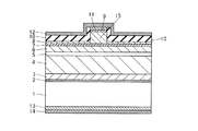
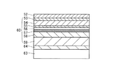
図1は、本発明の第1実施形態による窒化物系半導体レーザ素子(半導体素子)の構造を示した断面図である。図2は、図1に示した第1実施形態による窒化物系半導体レーザ素子の活性層の構造を示した断面図である。まず、図1および図2を参照して、第1実施形態による窒化物系半導体レーザ素子の構造について説明する。
(First embodiment)
FIG. 1 is a sectional view showing the structure of a nitride-based semiconductor laser device (semiconductor device) according to the first embodiment of the present invention. FIG. 2 is a sectional view showing the structure of the active layer of the nitride-based semiconductor laser device according to the first embodiment shown in FIG. First, the structure of the nitride-based semiconductor laser device according to the first embodiment will be described with reference to FIGS.
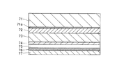
第1実施形態による窒化物系半導体レーザ素子では、図1に示すように、約100μmの厚みを有するAl0.07Ga0.93NからなるAlGaN基板1上に、約0.5nm〜約20nmの厚みを有するアンドープのAl0.15Ga0.85Nからなる高Al組成層2が形成されている。なお、高Al組成層2は、本発明の「窒化物系半導体層」の一例である。また、AlGaN基板1は、本発明の「半導体基板」の一例である。 In the nitride-based semiconductor laser device according to the first embodiment, as shown in FIG. 1, on an AlGaN substrate 1 made of Al 0.07 Ga 0.93 N having a thickness of about 100 μm, about 0.5 nm to about 20 nm. high Al composition layer 2 is formed of undoped with the thickness of the Al 0.15 Ga 0.85 N. The high Al composition layer 2 is an example of the “nitride-based semiconductor layer” in the present invention. The AlGaN substrate 1 is an example of the “semiconductor substrate” in the present invention.
ここで、第1実施形態では、高Al組成層2は、2種類の3族元素であるAlおよびGaと窒素とから構成されている。また、高Al組成層2とAlGaN基板1とは、同一の構成元素(Al、Ga、N)で構成されている。また、高Al組成層2のAl組成比(15%)は、AlGaN基板1のAl組成比(7%)よりも高くなるように構成されている。さらに、高Al組成層2は、AlGaN基板1上に接触するように形成されている。 Here, in the first embodiment, the high Al composition layer 2 is composed of two types of Group 3 elements, Al and Ga, and nitrogen. The high Al composition layer 2 and the AlGaN substrate 1 are composed of the same constituent elements (Al, Ga, N). The Al composition ratio (15%) of the high Al composition layer 2 is configured to be higher than the Al composition ratio (7%) of the AlGaN substrate 1. Furthermore, the high Al composition layer 2 is formed on the AlGaN substrate 1 so as to be in contact therewith.
高Al組成層2上には、約1.0μmの厚みを有するアンドープのAl0.01Ga0.99Nからなるバッファ層3が形成されている。バッファ層3上には、約2.0μmの厚みを有するGeがドープされたn型Al0.07Ga0.93Nからなるn型クラッド層4が形成されている。このn型クラッド層4は、AlGaN基板1と同一の元素(Al、Ga、N)により構成されているとともに、AlGaN基板1と同一のAl組成比(7%)を有する。なお、n型クラッド層4は、本発明の「クラッド層」の一例である。n型クラッド層4上には、MQW構造を有する活性層5が形成されている。活性層5は、図2に示すように、約3.5nmの厚みを有するアンドープのInXGa1−XNからなる3つの量子井戸層5aと、約20nmの厚みを有するアンドープのInYGa1−YNからなる3つの量子障壁層5bとが交互に積層されて構成されている。なお、X>Yであり、X=0.15、Y=0.02である。 A buffer layer 3 made of undoped Al 0.01 Ga 0.99 N having a thickness of about 1.0 μm is formed on the high Al composition layer 2. On the buffer layer 3, n-type cladding layer 4 Ge having a thickness of about 2.0μm is of doped n-type Al 0.07 Ga 0.93 N is formed. The n-type cladding layer 4 is composed of the same elements (Al, Ga, N) as the AlGaN substrate 1 and has the same Al composition ratio (7%) as the AlGaN substrate 1. The n-type cladding layer 4 is an example of the “cladding layer” in the present invention. An active layer 5 having an MQW structure is formed on the n-type cladding layer 4. As shown in FIG. 2, the active layer 5 includes three quantum well layers 5 a made of undoped In X Ga 1-X N having a thickness of about 3.5 nm, and undoped In Y Ga having a thickness of about 20 nm. Three quantum barrier layers 5b made of 1- YN are alternately stacked. Note that X> Y, X = 0.15, and Y = 0.02.
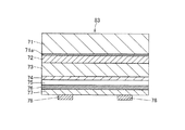
また、活性層5上には、図1に示すように、約80nmの厚みを有するアンドープのIn0.01Ga0.99Nからなるp側光ガイド層6が形成されている。p側光ガイド層6上には、約20nmの厚みを有するアンドープのAl0.2Ga0.8Nからなるp側キャリアブロック層7が形成されている。また、p側キャリアブロック層7上には、図1に示すように、平坦部と凸部とを有するMgがドープされたAl0.07Ga0.93Nからなるp型クラッド層8が形成されている。このp型クラッド層8の凸部の膜厚は、約0.45μmであり、p型クラッド層8の凸部以外の平坦部の膜厚は、約0.05μmである。このp型クラッド層8は、AlGaN基板1と同一の元素(Al、Ga、N)により構成されているとともに、AlGaN基板1と同一のAl組成比(7%)を有する。なお、p型クラッド層8は、本発明の「クラッド層」の一例である。p型クラッド層8の凸部の上面上には、約2nmの厚みを有するアンドープのIn0.07Ga0.93Nからなるp側コンタクト層9が形成されている。p型クラッド層8の凸部と、p側コンタクト層9とによって、電流通路となるリッジ部15が構成されている。このリッジ部15は、平面的に見て、光の出射方向に延びるストライプ状(細長状)に形成されている。また、リッジ部15は、約1.5μmの幅を有している。 Further, as shown in FIG. 1, a p-side light guide layer 6 made of undoped In 0.01 Ga 0.99 N having a thickness of about 80 nm is formed on the active layer 5. On the p-side light guide layer 6, a p-side carrier block layer 7 made of undoped Al 0.2 Ga 0.8 N having a thickness of about 20 nm is formed. Further, on the p-side carrier block layer 7, as shown in FIG. 1, a p-type cladding layer 8 made of Al 0.07 Ga 0.93 N doped with Mg and having a flat portion and a convex portion is formed. Has been. The film thickness of the convex part of the p-type cladding layer 8 is about 0.45 μm, and the film thickness of the flat part other than the convex part of the p-type cladding layer 8 is about 0.05 μm. The p-type cladding layer 8 is composed of the same elements (Al, Ga, N) as the AlGaN substrate 1 and has the same Al composition ratio (7%) as the AlGaN substrate 1. The p-type cladding layer 8 is an example of the “cladding layer” in the present invention. A p-side contact layer 9 made of undoped In 0.07 Ga 0.93 N having a thickness of about 2 nm is formed on the upper surface of the convex portion of the p-type cladding layer 8. The convex portion of the p-type cladding layer 8 and the p-side contact layer 9 constitute a ridge portion 15 serving as a current path. The ridge portion 15 is formed in a stripe shape (elongated shape) extending in the light emission direction when seen in a plan view. The ridge portion 15 has a width of about 1.5 μm.
また、リッジ部15の側面と、p型クラッド層8の平坦部の上面上とに、約0.2μmの厚みを有するSiO2膜からなる電流ブロック層10が形成されている。p側コンタクト層9の上面上には、下層から上層に向かって、約1nmの膜厚を有するSi層と、約20nmの膜厚を有するPd層と、約10nmの膜厚を有するAu層とからなるp側オーミック電極11が形成されている。 A current blocking layer 10 made of a SiO 2 film having a thickness of about 0.2 μm is formed on the side surface of the ridge portion 15 and the upper surface of the flat portion of the p-type cladding layer 8. On the upper surface of the p-side contact layer 9, from the lower layer to the upper layer, a Si layer having a thickness of about 1 nm, a Pd layer having a thickness of about 20 nm, and an Au layer having a thickness of about 10 nm, A p-side ohmic electrode 11 made of is formed.
また、p側オーミック電極11の上面上と、電流ブロック層10の上面上とに、p側オーミック電極11の上面に接触するように、下層から上層に向かって、約30nmの膜厚を有するTi層と、約150nmの膜厚を有するPd層と、約3000nmの膜厚を有するAu層とからなるp側パッド電極12が形成されている。 Further, Ti having a film thickness of about 30 nm from the lower layer to the upper layer so as to be in contact with the upper surface of the p-side ohmic electrode 11 on the upper surface of the p-side ohmic electrode 11 and on the upper surface of the current blocking layer 10. A p-side pad electrode 12 composed of a layer, a Pd layer having a thickness of about 150 nm, and an Au layer having a thickness of about 3000 nm is formed.
また、AlGaN基板1の裏面上には、図1に示すように、AlGaN基板1の裏面に近い方から順に、約1nmの膜厚を有するSi層と、約6nmの膜厚を有するAl層と、約30nmの膜厚を有するPd層とからなるn側オーミック電極13が形成されている。n側オーミック電極13の裏面上には、約300nmの膜厚を有するAu層からなるn側パッド電極14が形成されている。 Further, on the back surface of the AlGaN substrate 1, as shown in FIG. 1, an Si layer having a thickness of about 1 nm, an Al layer having a thickness of about 6 nm, in order from the side close to the back surface of the AlGaN substrate 1, An n-side ohmic electrode 13 made of a Pd layer having a thickness of about 30 nm is formed. An n-side pad electrode 14 made of an Au layer having a thickness of about 300 nm is formed on the back surface of the n-side ohmic electrode 13.
第1実施形態では、上記のように、Al0.07Ga0.93NからなるAlGaN基板1の上面に、AlGaN基板1の構成元素と同一の構成元素(Al、Ga、N)からなり、かつ、Al組成比がAlGaN基板1のAl組成比よりも高い高Al組成層2を設けることによって、Alは、Gaに比べて窒素との結合力が強い性質を有するため、高Al組成層2上に窒化物系半導体レーザ素子を構成するバッファ層3を成長させる際に、バッファ層3の構成元素である窒素を容易に高Al組成層2のAlに結合させることができる。このため、高Al組成層2上に形成する窒化物系半導体レーザ素子を構成するバッファ層3中にピットが発生するのを抑制することができるので、窒化物系半導体レーザ素子の素子特性の低下を抑制することができる。 In the first embodiment, as described above, the upper surface of the AlGaN substrate 1 made of Al 0.07 Ga 0.93 N is made of the same constituent elements (Al, Ga, N) as the constituent elements of the AlGaN substrate 1. In addition, by providing the high Al composition layer 2 having an Al composition ratio higher than the Al composition ratio of the AlGaN substrate 1, Al has a property of having a stronger binding force with nitrogen than Ga. When the buffer layer 3 constituting the nitride-based semiconductor laser element is grown thereon, nitrogen, which is a constituent element of the buffer layer 3, can be easily bonded to Al of the high Al composition layer 2. For this reason, it is possible to suppress the generation of pits in the buffer layer 3 constituting the nitride semiconductor laser element formed on the high Al composition layer 2, so that the device characteristics of the nitride semiconductor laser element are degraded. Can be suppressed.
また、第1実施形態では、AlGaN基板1の上面に形成される高Al組成層2のAl組成比を、AlGaN基板1のAl組成比よりも高くすることによって、高Al組成層2を、AlGaN基板1よりも硬くすることができるので、AlGaN基板1と高Al組成層2との界面で、AlGaN基板1に存在する転位を曲げることができる。これにより、AlGaN基板1に存在する転位が、高Al組成層2を越えて上層のバッファ層3、n型クラッド層4、活性層5、p側光ガイド層6、p側キャリアブロック層7、p型クラッド層8およびp側コンタクト層9に伝播するのを抑制することができる。これによっても、窒化物系半導体レーザ素子の素子特性の低下を抑制することができる。 In the first embodiment, the Al composition ratio of the high Al composition layer 2 formed on the upper surface of the AlGaN substrate 1 is made higher than the Al composition ratio of the AlGaN substrate 1, so that the high Al composition layer 2 Since it can be harder than the substrate 1, dislocations existing in the AlGaN substrate 1 can be bent at the interface between the AlGaN substrate 1 and the high Al composition layer 2. As a result, dislocations existing in the AlGaN substrate 1 exceed the high Al composition layer 2 and are an upper buffer layer 3, an n-type cladding layer 4, an active layer 5, a p-side light guide layer 6, a p-side carrier block layer 7, Propagation to the p-type cladding layer 8 and the p-side contact layer 9 can be suppressed. Also by this, it is possible to suppress deterioration of element characteristics of the nitride-based semiconductor laser element.
また、第1実施形態では、AlGaN基板1の構成元素と同一の構成元素からなるn型クラッド層4およびp型クラッド層8をさらに備えることによって、n型クラッド層4およびp型クラッド層8とAlGaN基板1との格子定数差を小さくすることができるので、n型クラッド層4およびp型クラッド層8とAlGaN基板1との格子定数差に起因して生じるAlGaN基板1の反りおよびクラックの発生を容易に抑制することができる。 In the first embodiment, the n-type cladding layer 4 and the p-type cladding layer 8 are further provided with the n-type cladding layer 4 and the p-type cladding layer 8 made of the same constituent elements as the constituent elements of the AlGaN substrate 1. Since the lattice constant difference with the AlGaN substrate 1 can be reduced, warping and cracking of the AlGaN substrate 1 caused by the lattice constant difference between the n-type cladding layer 4 and the p-type cladding layer 8 and the AlGaN substrate 1 are generated. Can be easily suppressed.
また、第1実施形態では、高Al組成層2を、AlGaN基板1の上面上に接触するように形成することによって、AlGaN基板1中に存在する転位を、AlGaN基板1の直上に形成された高Al組成層2によって曲げることができるので、高Al組成層2条に形成されるバッファ層3、n型クラッド層4、活性層5、p側光ガイド層6、p側キャリアブロック層7、p型クラッド層8およびp側コンタクト層9に転位が伝播するのを有効に抑制することができる。 In the first embodiment, the dislocations present in the AlGaN substrate 1 are formed immediately above the AlGaN substrate 1 by forming the high Al composition layer 2 in contact with the upper surface of the AlGaN substrate 1. Since it can be bent by the high Al composition layer 2, the buffer layer 3, the n-type cladding layer 4, the active layer 5, the p-side light guide layer 6, the p-side carrier block layer 7, It is possible to effectively suppress dislocations from propagating to the p-type cladding layer 8 and the p-side contact layer 9.
図3〜図6は、図1に示した第1実施形態による窒化物系半導体レーザ素子の製造プロセスを説明するための断面図である。次に、図1および図3〜図6を参照して、第1実施形態による窒化物系半導体レーザ素子の製造プロセスについて説明する。 3 to 6 are cross-sectional views for explaining a manufacturing process of the nitride-based semiconductor laser device according to the first embodiment shown in FIG. A manufacturing process for the nitride-based semiconductor laser device according to the first embodiment is now described with reference to FIGS.
まず、図3に示すように、有機金属気相エピタキシー(MOVPE)法を用いて、Al0.07Ga0.93NからなるAlGaN基板1上に、高Al組成層2、バッファ層3、n型クラッド層4、活性層5、p側光ガイド層6、p側キャリアブロック層7、p型クラッド層8およびp側コンタクト層9を順次成長させる。 First, as shown in FIG. 3, a high Al composition layer 2, a buffer layer 3, and n are formed on an AlGaN substrate 1 made of Al 0.07 Ga 0.93 N by using a metal organic vapor phase epitaxy (MOVPE) method. The type cladding layer 4, the active layer 5, the p-side light guide layer 6, the p-side carrier block layer 7, the p-type cladding layer 8 and the p-side contact layer 9 are grown sequentially.
具体的には、AlGaN基板1を、H2およびNH3雰囲気の反応炉の中に挿入し、NH3ガスを供給した状態で、約1000℃〜約1200℃(たとえば、約1150℃)の単結晶成長温度まで加熱する。AlGaN基板1の温度が約1150℃に達すると、水素からなるキャリアガスと、トリメチルガリウム(TMGa)およびトリメチルアルミニウム(TMAl)からなる原料ガスとを用いて、AlGaN基板1の(0001)面上に約0.5nm〜約20nmの厚みを有するアンドープのAl0.15Ga0.85Nからなる高Al組成層2を成長させる。次に、AlGaN基板1を約1150℃に保持した状態で、高Al組成層2上に、約1.0μmの厚みを有するアンドープのAl0.01Ga0.99Nからなるバッファ層3を成長させる。その後、AlGaN基板1を約1150℃に保持した状態で、水素からなるキャリアガスと、TMGa、TMAlおよびn型導電性を得るためのGe不純物の原料であるGeH4(モノゲルマン)からなる原料ガスとを用いて、バッファ層3上に、約2.0μmの厚みを有するGeがドープされたAl0.07Ga0.93Nからなるn型クラッド層4を成長させる。 Specifically, the AlGaN substrate 1 is inserted into a reaction furnace in an atmosphere of H 2 and NH 3 and supplied with NH 3 gas, and a single temperature of about 1000 ° C. to about 1200 ° C. (for example, about 1150 ° C.). Heat to crystal growth temperature. When the temperature of the AlGaN substrate 1 reaches about 1150 ° C., a carrier gas composed of hydrogen and a source gas composed of trimethylgallium (TMGa) and trimethylaluminum (TMAl) are used on the (0001) plane of the AlGaN substrate 1. A high Al composition layer 2 made of undoped Al 0.15 Ga 0.85 N having a thickness of about 0.5 nm to about 20 nm is grown. Next, a buffer layer 3 made of undoped Al 0.01 Ga 0.99 N having a thickness of about 1.0 μm is grown on the high Al composition layer 2 while the AlGaN substrate 1 is held at about 1150 ° C. Let Thereafter, in a state where the AlGaN substrate 1 is held at about 1150 ° C., a source gas made of carrier gas made of hydrogen and GeH 4 (monogermane) which is a raw material of Ge impurities for obtaining TMGa, TMAl and n-type conductivity. Then, the n-type cladding layer 4 made of Al 0.07 Ga 0.93 N doped with Ge having a thickness of about 2.0 μm is grown on the buffer layer 3.
次に、AlGaN基板1を約850℃に保持した状態で、トリエチルガリウム(TEGa)およびトリメチルインジウム(TMIn)からなる原料ガスを用いて、n型クラッド層4上に、約3.5nmの厚みを有するアンドープIn0.15Ga0.85Nからなる3層の量子井戸層5aと、約20nmの厚みを有するアンドープIn0.02Ga0.98Nからなる3層の量子障壁層5bとを交互に成長させることによりMQW構造を有する活性層5を形成する。 Next, a thickness of about 3.5 nm is formed on the n-type cladding layer 4 using a source gas composed of triethylgallium (TEGa) and trimethylindium (TMIn) while the AlGaN substrate 1 is held at about 850 ° C. Three quantum well layers 5a made of undoped In 0.15 Ga 0.85 N and three quantum barrier layers 5b made of undoped In 0.02 Ga 0.98 N having a thickness of about 20 nm are alternately arranged. The active layer 5 having the MQW structure is formed.
次に、AlGaN基板1を約850℃に保持した状態で、活性層5上に、約80nmの厚みを有するアンドープのIn0.01Ga0.99Nからなるp側光ガイド層6を成長させる。次に、TMGaおよびTMAlからなる原料ガスを用いて、約20nmの厚みを有するAl0.25Ga0.75Nからなるキャリアブロック層7を成長させる。 Next, a p-side light guide layer 6 made of undoped In 0.01 Ga 0.99 N having a thickness of about 80 nm is grown on the active layer 5 with the AlGaN substrate 1 held at about 850 ° C. . Next, a carrier block layer 7 made of Al 0.25 Ga 0.75 N having a thickness of about 20 nm is grown using a source gas made of TMGa and TMAl.
次に、H2およびNH3雰囲気中において、AlGaN基板1を約1150℃に保持した状態で、キャリアブロック層7上に、p型不純物のMgの原料であるCp2Mg、TMGaおよびTMAlからなる原料ガスを用いて、約0.45μmの厚みを有するMgがドープされたAl0.07Ga0.93Nからなるp型クラッド層8を成長させる。 Next, in an atmosphere of H 2 and NH 3 , with the AlGaN substrate 1 held at about 1150 ° C., the carrier block layer 7 is made of Cp 2 Mg, TMGa and TMAl, which are raw materials for Mg of p-type impurities. A p-type cladding layer 8 made of Al 0.07 Ga 0.93 N doped with Mg having a thickness of about 0.45 μm is grown using a source gas.
次に、AlGaN基板1を約850℃に保持した状態で、NH3雰囲気において、p型クラッド層8上に、TEGaおよびTMInからなる原料ガスを用いて、約2nmの厚みを有するアンドープのIn0.07Ga0.93Nからなるp側コンタクト層9を成長させる。 Next, an undoped In 0 having a thickness of about 2 nm is formed on the p-type cladding layer 8 using a source gas composed of TEGa and TMIn in an NH 3 atmosphere while the AlGaN substrate 1 is held at about 850 ° C. A p-side contact layer 9 made of 0.07 Ga 0.93 N is grown.
この後、図4に示すように、プラズマCVD法などを用いて、p側コンタクト層9上に、約1.5μmの幅を有するSiO2膜10aを形成する。そして、SiO2膜10aをマスクとして、Cl2ガスによる反応性イオンエッチング(RIE)法により、p側コンタクト層9およびp型クラッド層8の一部をエッチングすることにより、図5に示されるようなp側コンタクト層9とp型クラッド層8の凸部とからなるリッジ部15が形成される。この場合、p型クラッド層8の凸部は、約0.45μmの膜厚とするとともに、p型クラッド層8の平坦部の膜厚が約0.05μmとなるように、エッチング深さを制御する。この後、SiO2膜10aを除去する。 Thereafter, as shown in FIG. 4, a SiO 2 film 10a having a width of about 1.5 μm is formed on the p-side contact layer 9 by using a plasma CVD method or the like. Then, by using the SiO 2 film 10a as a mask, a part of the p-side contact layer 9 and the p-type cladding layer 8 is etched by reactive ion etching (RIE) using Cl 2 gas, as shown in FIG. A ridge portion 15 including the p-side contact layer 9 and the convex portion of the p-type cladding layer 8 is formed. In this case, the protrusion depth of the p-type cladding layer 8 has a thickness of about 0.45 μm, and the etching depth is controlled so that the thickness of the flat portion of the p-type cladding layer 8 is about 0.05 μm. To do. Thereafter, the SiO 2 film 10a is removed.
次に、図6に示すように、プラズマCVD法を用いて、約0.2μmの膜厚を有するSiO2膜を全面に形成した後、フォトリソグラフィー技術と、Cl2ガスによるRIE法とを用いて、p側コンタクト層9の上面が露出するようにSiO2膜の一部を除去することによって、SiO2膜からなる電流ブロック層10が形成される。 Next, as shown in FIG. 6, after a SiO 2 film having a thickness of about 0.2 μm is formed on the entire surface by plasma CVD, photolithography and RIE using Cl 2 gas are used. Thus, by removing a part of the SiO 2 film so that the upper surface of the p-side contact layer 9 is exposed, the current blocking layer 10 made of the SiO 2 film is formed.
次に、図1に示したように、p側コンタクト層9の上面上に、電子ビーム加熱蒸着法を用いて、下層から上層に向かって、約1nmの膜厚を有するSi層と、約20nmの膜厚を有するPd層と、約10nmの膜厚を有するAu層とからなるp側オーミック電極11を形成する。そして、電子ビーム加熱蒸着法を用いて、p側オーミック電極11の上面上と、電流ブロック層10の上面上とに、p側オーミック電極11の上面に接触するように、下層から上層に向かって、約30nmの膜厚を有するTi層と、約150nmの膜厚を有するPd層と、約3000nmの膜厚を有するAu層とからなるp側パッド電極12を形成する。そして、AlGaN基板1の裏面を、劈開し易い厚みまで研磨する。その後、図1に示すように、電子ビーム加熱蒸着法を用いて、AlGaN基板1の裏面に近い側から、約1nmの膜厚を有するSi層と、約6nmの膜厚を有するAl層と、約30nmの膜厚を有するPd層とからなるn側オーミック電極13を形成する。そして、電子ビーム加熱蒸着法を用いて、n側オーミック電極13の裏面に接触するように、約300nmの厚みを有するAu層からなるn側パッド電極14を形成する。これにより、図1に示したような、第1実施形態による窒化物系半導体レーザ素子が完成される。 Next, as shown in FIG. 1, an Si layer having a thickness of about 1 nm is formed on the upper surface of the p-side contact layer 9 from the lower layer to the upper layer using an electron beam heating deposition method, and about 20 nm. A p-side ohmic electrode 11 composed of a Pd layer having a thickness of about 10 nm and an Au layer having a thickness of about 10 nm is formed. Then, from the lower layer to the upper layer using the electron beam heating vapor deposition method, the upper surface of the p-side ohmic electrode 11 and the upper surface of the current blocking layer 10 are in contact with the upper surface of the p-side ohmic electrode 11. Then, the p-side pad electrode 12 including a Ti layer having a thickness of about 30 nm, a Pd layer having a thickness of about 150 nm, and an Au layer having a thickness of about 3000 nm is formed. Then, the back surface of the AlGaN substrate 1 is polished to a thickness that can be easily cleaved. Thereafter, as shown in FIG. 1, using an electron beam heating vapor deposition method, from the side close to the back surface of the AlGaN substrate 1, an Si layer having a thickness of about 1 nm, an Al layer having a thickness of about 6 nm, An n-side ohmic electrode 13 composed of a Pd layer having a thickness of about 30 nm is formed. Then, an n-side pad electrode 14 made of an Au layer having a thickness of about 300 nm is formed so as to be in contact with the back surface of the n-side ohmic electrode 13 by using an electron beam heating vapor deposition method. Thereby, the nitride-based semiconductor laser device according to the first embodiment as shown in FIG. 1 is completed.
(第2実施形態)
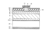
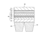
図7は、本発明の第2実施形態による窒化物系半導体レーザ素子の構造を示した断面図である。図7を参照して、この第2実施形態では、上記第1実施形態と異なり、高Al組成層21aが、AlGaN基板21の表面が変質された変質層からなる場合の構造について説明する。なお、第2実施形態のAlGaN基板21および高Al組成層21a以外の構造は、上記第1実施形態と同じであるため、高Al組成層21a以外の構造については説明を省略する。なお、AlGaN基板21は、本発明の「半導体基板」の一例である。
(Second Embodiment)
FIG. 7 is a cross-sectional view showing the structure of a nitride-based semiconductor laser device according to the second embodiment of the present invention. With reference to FIG. 7, in the second embodiment, unlike the first embodiment, a structure in which the high Al composition layer 21a is composed of an altered layer in which the surface of the AlGaN substrate 21 is altered will be described. In addition, since structures other than the AlGaN substrate 21 and the high Al composition layer 21a of the second embodiment are the same as those of the first embodiment, description of the structures other than the high Al composition layer 21a is omitted. The AlGaN substrate 21 is an example of the “semiconductor substrate” in the present invention.
この第2実施形態では、図7に示すように、約100μmの厚みを有するAl0.07Ga0.93NからなるAlGaN基板21の上面に、高Al組成層21aが形成されている。なお、高Al組成層21aは、本発明の「窒化物系半導体層」の一例である。この高Al組成層21aは、Al0.07Ga0.93NからなるAlGaN基板21の表面が変質されることにより、Al組成比が増加された変質層からなる。また、この変質層は、AlGaN基板21と変質層との界面(Al組成比7%)から変質層の上面に向かって、Alの組成比が徐々に増加しており、変質層の上面近傍でのAl組成比が最も高くなっている。この変質層の上面近傍のAl組成比の値は、約20%である。また、高Al組成層21aの厚みは、約2nmである。 In the second embodiment, as shown in FIG. 7, a high Al composition layer 21a is formed on the upper surface of an AlGaN substrate 21 made of Al 0.07 Ga 0.93 N having a thickness of about 100 μm. The high Al composition layer 21a is an example of the “nitride-based semiconductor layer” in the present invention. The high Al composition layer 21a is a modified layer in which the Al composition ratio is increased by altering the surface of the AlGaN substrate 21 made of Al 0.07 Ga 0.93 N. Further, in this altered layer, the Al composition ratio gradually increases from the interface between the AlGaN substrate 21 and the altered layer (Al composition ratio 7%) toward the upper surface of the altered layer. The Al composition ratio is the highest. The value of the Al composition ratio in the vicinity of the upper surface of the deteriorated layer is about 20%. The thickness of the high Al composition layer 21a is about 2 nm.
第2実施形態では、上記のように、高Al組成層21aを、AlGaN基板21の表面が変質された変質層からなるように構成することによって、AlGaN基板21上に高Al組成層21aを結晶成長させることなく、ピットの発生および転位の伝播を抑制可能な高Al組成層21aを形成することができる。 In the second embodiment, as described above, the high Al composition layer 21a is formed of an altered layer in which the surface of the AlGaN substrate 21 is altered, so that the high Al composition layer 21a is crystallized on the AlGaN substrate 21. Without the growth, it is possible to form the high Al composition layer 21a capable of suppressing the generation of pits and the propagation of dislocations.
なお、第2実施形態のその他の効果は、上記第1実施形態と同様である。 The remaining effects of the second embodiment are similar to those of the aforementioned first embodiment.
次に、第2実施形態による窒化物系半導体レーザ素子の製造プロセスについて説明する。まず、Al0.07Ga0.93NからなるAlGaN基板21を、H2およびNH3雰囲気の反応炉の中に挿入し、窒化物系半導体層の窒素原料であるNH3ガスを供給した状態で、AlGaN基板21を約1000℃〜約1200℃の間の温度(たとえば、約1150℃)まで加熱する。この際、NH3流量はAlGaN成長に必要な流量(約6SLM)(SLM(Standard Liter per Minutes:1気圧、25℃における1分間辺りの流量をリットルで表示した単位))の約50%の約3SLMとする。NH3流量が少ない状態で基板温度を約1150℃にまで上昇することにより、Al0.07Ga0.93NからなるAlGaN基板21の表面のNおよびGaが熱によりAlGaN基板21から離脱する一方、AlGaNの中で熱的に安定なAlが脱離せずに残る。これにより、Al0.07Ga0.93NからなるAlGaN基板21の表面が変質されてAl組成比の高いAlGaN層(変質層)からなる高Al組成層21aが形成される。 Next, a manufacturing process for the nitride-based semiconductor laser device according to the second embodiment will be described. First, an AlGaN substrate 21 made of Al 0.07 Ga 0.93 N is inserted into a reaction furnace in an atmosphere of H 2 and NH 3, and NH 3 gas that is a nitrogen raw material for a nitride-based semiconductor layer is supplied Then, the AlGaN substrate 21 is heated to a temperature between about 1000 ° C. and about 1200 ° C. (for example, about 1150 ° C.). At this time, the NH 3 flow rate is about 50% of the flow rate required for AlGaN growth (about 6 SLM) (SLM (Standard Liter per Minutes: 1 atm, flow rate per minute at 25 ° C. expressed in liters)). Let it be 3SLM. By increasing the substrate temperature to about 1150 ° C. with a small NH 3 flow rate, N and Ga on the surface of the AlGaN substrate 21 made of Al 0.07 Ga 0.93 N are separated from the AlGaN substrate 21 by heat. In AlGaN, thermally stable Al remains without desorbing. Thereby, the surface of the AlGaN substrate 21 made of Al 0.07 Ga 0.93 N is altered to form a high Al composition layer 21a made of an AlGaN layer (modified layer) having a high Al composition ratio.
次に、AlGaN基板21を約1150℃の温度に保持した状態で、水素からなるキャリアガスと、TMGaおよびTMAlからなる原料ガスとを用いて、高Al組成層21a上に、約1.0μmの厚みを有するアンドープのAl0.01Ga0.99Nからなるバッファ層3を成長させる。 Next, with the AlGaN substrate 21 held at a temperature of about 1150 ° C., a carrier gas composed of hydrogen and a source gas composed of TMGa and TMAl are used to form about 1.0 μm on the high Al composition layer 21a. A buffer layer 3 made of undoped Al 0.01 Ga 0.99 N having a thickness is grown.
第2実施形態のバッファ層3の形成後の製造プロセスは、上記第1実施形態と同様である。 The manufacturing process after the formation of the buffer layer 3 of the second embodiment is the same as that of the first embodiment.
なお、AlGaN基板21の表面を変質させることによって、AlGaN基板21の表面に変質層からなる高Al組成層21aを形成する方法としては、上記した第2実施形態の方法以外に以下の3つの第1変形例〜第3変形例による方法がある。 In addition to the method of the second embodiment described above, the following three methods can be used to form the high Al composition layer 21a composed of the altered layer on the surface of the AlGaN substrate 21 by altering the surface of the AlGaN substrate 21. There is a method according to a first modification to a third modification.
第2実施形態の第1変形例による方法としては、Al0.07Ga0.93NからなるAlGaN基板21を、H2およびNH3雰囲気の反応炉の中に挿入し、窒化物系半導体層の成長に必要なH2流量(約20SLM)の約2倍の約40SLMのH2を流した状態で、AlGaN基板21を約1000℃〜約1200℃の間の温度(たとえば、約1150℃)まで加熱する。H2流量が多い状態で、AlGaN基板21温度を約1150℃まで上昇することにより、Al0.07Ga0.93NからなるAlGaN基板21の表面のNおよびGaが熱によりAlGaN基板21から脱離する一方、AlGaNの中で熱的に安定なAlが脱離せずに残る。これにより、Al0.07Ga0.93NからなるAlGaN基板21の表面が変質されてAl組成比の高いAlGaN層(変質層)からなる高Al組成層21aが形成される。 As a method according to the first modification of the second embodiment, an AlGaN substrate 21 made of Al 0.07 Ga 0.93 N is inserted into a reaction furnace in an H 2 and NH 3 atmosphere, and a nitride-based semiconductor layer is formed. The AlGaN substrate 21 is heated to a temperature between about 1000 ° C. and about 1200 ° C. (eg, about 1150 ° C.) with about 40 SLM of H 2 flowing about twice as much as the H 2 flow rate (about 20 SLM) required for the growth of the substrate. Until heated. By increasing the temperature of the AlGaN substrate 21 to about 1150 ° C. with a high H 2 flow rate, N and Ga on the surface of the AlGaN substrate 21 made of Al 0.07 Ga 0.93 N are removed from the AlGaN substrate 21 by heat. On the other hand, thermally stable Al remains in AlGaN without desorption. Thereby, the surface of the AlGaN substrate 21 made of Al 0.07 Ga 0.93 N is altered to form a high Al composition layer 21a made of an AlGaN layer (modified layer) having a high Al composition ratio.
また、第2実施形態の第2変形例による方法としては、Al0.07Ga0.93NからなるAlGaN基板21を、H2およびNH3雰囲気の反応炉の中に挿入し、AlGaN基板21を約1000℃〜約1200℃の間の温度(たとえば、約1150℃)まで加熱する。AlGaN基板21温度が約1150℃に達した後、NH3流量をAlGaN成長に必要な流量の約50%の約3SLMとして約5分間保持する。これにより、Al0.07Ga0.93NからなるAlGaN基板21表面のNおよびGaが熱によりAlGaN基板21から脱離する一方、AlGaNの中で熱的に安定なAlが脱離せずに残る。これにより、Al0.07Ga0.93NからなるAlGaN基板21の表面が変質されてAl組成比の高いAlGaN層(変質層)からなる高Al組成層21aが形成される。 Further, as a method according to the second modification of the second embodiment, an AlGaN substrate 21 made of Al 0.07 Ga 0.93 N is inserted into a reaction furnace in an atmosphere of H 2 and NH 3 , and the AlGaN substrate 21 Is heated to a temperature between about 1000 ° C. and about 1200 ° C. (eg, about 1150 ° C.). After the temperature of the AlGaN substrate 21 reaches about 1150 ° C., the NH 3 flow rate is held at about 3 SLM, which is about 50% of the flow rate required for AlGaN growth, and is held for about 5 minutes. Thereby, N and Ga on the surface of the AlGaN substrate 21 made of Al 0.07 Ga 0.93 N are desorbed from the AlGaN substrate 21 by heat, while thermally stable Al remains in the AlGaN without desorption. . Thereby, the surface of the AlGaN substrate 21 made of Al 0.07 Ga 0.93 N is altered to form a high Al composition layer 21a made of an AlGaN layer (modified layer) having a high Al composition ratio.
また、第2実施形態の第3変形例による方法としては、Al0.07Ga0.93NからなるAlGaN基板21を、H2およびNH3雰囲気の反応炉の中に挿入し、AlGaN基板21を約1000℃〜約1200℃の間の温度(たとえば、約1150℃)まで加熱する。AlGaN基板21温度が約1150℃に達した後、AlGaN基板21温度を約1150℃に保持した状態で、H2流量をAlGaN層の成長に必要な流量の約2倍の約40SLMとして約5分間保持する。これにより、Al0.07Ga0.93NからなるAlGaN基板21の表面のNおよびGaを熱によりAlGaN基板21の表面から脱離する一方、AlGaNの中で熱的に安定なAlが脱離せずに残る。これにより、Al0.07Ga0.93NからなるAlGaN基板21の表面が変質されてAl組成比の高いAlGaN層(変質層)からなる高Al組成層21aが形成される。 Further, as a method according to the third modification of the second embodiment, an AlGaN substrate 21 made of Al 0.07 Ga 0.93 N is inserted into a reaction furnace in an atmosphere of H 2 and NH 3 , and the AlGaN substrate 21 Is heated to a temperature between about 1000 ° C. and about 1200 ° C. (eg, about 1150 ° C.). After the temperature of the AlGaN substrate 21 reaches about 1150 ° C., with the AlGaN substrate 21 temperature maintained at about 1150 ° C., the H 2 flow rate is about 40 SLM, which is about twice the flow rate required for the growth of the AlGaN layer, for about 5 minutes. Hold. As a result, N and Ga on the surface of the AlGaN substrate 21 made of Al 0.07 Ga 0.93 N are desorbed from the surface of the AlGaN substrate 21 by heat, while thermally stable Al is desorbed in the AlGaN. Remains. Thereby, the surface of the AlGaN substrate 21 made of Al 0.07 Ga 0.93 N is altered to form a high Al composition layer 21a made of an AlGaN layer (modified layer) having a high Al composition ratio.
(第3実施形態)
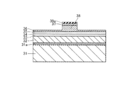
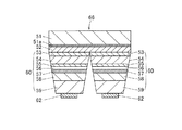
図8は、本発明の第3実施形態による窒化物系半導体レーザ素子(半導体素子)の構造を示した断面図である。図8を参照して、この第3実施形態では、上記第1および第2実施形態とは異なり、InGaN基板31上に変質層からなる高Ga組成層31aを形成した場合について説明する。
(Third embodiment)
FIG. 8 is a cross-sectional view showing the structure of a nitride-based semiconductor laser device (semiconductor device) according to the third embodiment of the present invention. Referring to FIG. 8, in the third embodiment, unlike the first and second embodiments, a case where a high Ga composition layer 31a made of an altered layer is formed on an InGaN substrate 31 will be described.
第3実施形態による窒化物系半導体レーザ素子では、図8に示すように、約100μm〜約200μmの厚みを有するIn0.15Ga0.85NからなるInGaN基板31上に、高Ga組成層31aが形成されている。なお、高Ga組成層31aは、本発明の「窒化物系半導体層」の一例である。また、InGaN基板31は、本発明の「半導体基板」の一例である。 In the nitride-based semiconductor laser device according to the third embodiment, as shown in FIG. 8, a high Ga composition layer is formed on an InGaN substrate 31 made of In 0.15 Ga 0.85 N having a thickness of about 100 μm to about 200 μm. 31a is formed. The high Ga composition layer 31a is an example of the “nitride-based semiconductor layer” in the present invention. The InGaN substrate 31 is an example of the “semiconductor substrate” in the present invention.
ここで、第3実施形態では、高Ga組成層31aは、In0.15Ga0.85NからなるInGaN基板31の表面が変質されることによりGa組成比が増加された変質層からなる。また、この変質層は、InGaN基板31と変質層との界面(Ga組成比85%)から変質層の上面に向かってGaの組成比が徐々に増加しており、変質層の上面近傍でのGa組成比が最も高くなっている。この変質層の上面近傍のGa組成比の値は、約92%である。また、高Ga組成層31aの厚みは、約5nmである。また、高Ga組成層31aは、InGaN基板31と同一の構成元素(In、Ga、N)から構成されているとともに、高Ga組成層31aの表面近傍のGa組成比(92%)は、InGaN基板31のGa組成比(85%)に比べて、高くなるように構成されている。 Here, in the third embodiment, the high Ga composition layer 31a is a modified layer in which the Ga composition ratio is increased by modifying the surface of the InGaN substrate 31 made of In 0.15 Ga 0.85 N. Further, in this altered layer, the Ga composition ratio gradually increases from the interface between the InGaN substrate 31 and the altered layer (Ga composition ratio 85%) toward the upper surface of the altered layer. The Ga composition ratio is the highest. The value of the Ga composition ratio in the vicinity of the upper surface of the deteriorated layer is about 92%. The thickness of the high Ga composition layer 31a is about 5 nm. The high Ga composition layer 31a is composed of the same constituent elements (In, Ga, N) as the InGaN substrate 31, and the Ga composition ratio (92%) near the surface of the high Ga composition layer 31a is InGaN. It is configured to be higher than the Ga composition ratio (85%) of the substrate 31.
また、高Ga組成層31a上には、約1μmの厚みを有するSiがドープされたIn0.1Ga0.9Nからなるn型クラッド層32が形成されている。n型クラッド層32上には、約50nmの厚みを有するSiがドープされたIn0.15Ga0.85Nからなるn型光導波層33が形成されている。n型光導波層33上には、MQW構造を有する活性層34が形成されている。この活性層34は、約2.5nmの厚みを有するIn0.3Ga0.7Nからなる2つの量子井戸層と、約15nmの厚みを有するIn0.17Ga0.83Nからなる3つの量子障壁層とが交互に積層されて構成されている。 An n-type cladding layer 32 made of In 0.1 Ga 0.9 N doped with Si having a thickness of about 1 μm is formed on the high Ga composition layer 31a. An n-type optical waveguide layer 33 made of In 0.15 Ga 0.85 N doped with Si having a thickness of about 50 nm is formed on the n-type cladding layer 32. An active layer 34 having an MQW structure is formed on the n-type optical waveguide layer 33. The active layer 34 includes two quantum well layers made of In 0.3 Ga 0.7 N having a thickness of about 2.5 nm, and 3 made of In 0.17 Ga 0.83 N having a thickness of about 15 nm. Two quantum barrier layers are alternately stacked.
また、活性層34上には、約50nmの厚みを有するアンドープのIn0.15Ga0.85Nからなるp型光導波層35が形成されている。p型光導波層35上には、Mgがドープされた約2.5nmの厚みを有するIn0.1Ga0.9N層と約2.5nmの厚みを有するGaN層との60周期の超格子クラッド層36が形成されている。超格子クラッド層36は、図8に示すように、平坦部と凸部とを有している。また、超格子クラッド層36上には、約0.1μmの厚みを有するMgがドープされたGaNからなるp型コンタクト層37が形成されている。超格子クラッド層36の凸部と、p型コンタクト層37とによって、電流通路となるリッジ部38が構成されている。このリッジ部38は、平面的に見て、光の出射方向に延びるストライプ状(細長状)に形成されている。 A p-type optical waveguide layer 35 made of undoped In 0.15 Ga 0.85 N having a thickness of about 50 nm is formed on the active layer 34. On the p-type optical waveguide layer 35, an over 0.1 layer of an In 0.1 Ga 0.9 N layer having a thickness of about 2.5 nm doped with Mg and a GaN layer having a thickness of about 2.5 nm is formed. A lattice cladding layer 36 is formed. As shown in FIG. 8, the superlattice cladding layer 36 has a flat portion and a convex portion. A p-type contact layer 37 made of GaN doped with Mg having a thickness of about 0.1 μm is formed on the superlattice cladding layer 36. The convex portion of the superlattice clad layer 36 and the p-type contact layer 37 constitute a ridge portion 38 serving as a current path. The ridge portion 38 is formed in a stripe shape (elongated shape) extending in the light emission direction when seen in a plan view.
また、リッジ部38の上面の一部および側面と、超格子クラッド層36の平坦部の上面上とに、SiO2膜からなる電流ブロック層39が形成されている。また、p型コンタクト層37の上面上および電流ブロック層39の上面上には、p型コンタクト層37に近い方からNi層とAu層とからなるp側電極40が形成されている。 In addition, a current blocking layer 39 made of a SiO 2 film is formed on a part of the upper surface and side surfaces of the ridge portion 38 and on the upper surface of the flat portion of the superlattice cladding layer 36. A p-side electrode 40 composed of a Ni layer and an Au layer is formed on the upper surface of the p-type contact layer 37 and the upper surface of the current blocking layer 39 from the side closer to the p-type contact layer 37.
また、InGaN基板31の裏面上には、図8に示すように、InGaN基板31の裏面に近い方から順に、Ti層と、Au層とからなるn側電極41が形成されている。 Further, on the back surface of the InGaN substrate 31, as shown in FIG. 8, an n-side electrode 41 composed of a Ti layer and an Au layer is formed in order from the side closer to the back surface of the InGaN substrate 31.
第3実施形態では、上記のように、高Ga組成層31aのGa組成比を、InGaN基板31のGa組成比より高くすることによって、Gaは、Inに比べて窒素との結合力が強い性質を有するため、高Ga組成層31a上に窒化物系半導体レーザ素子を構成するn型クラッド層32を成長させる際に、n型クラッド層32の構成元素である窒素を容易に下層の高Ga組成層31aのGaに結合させることができる。このため、高Ga組成層31a上に形成する窒化物系半導体レーザ素子を構成するn型クラッド層32中にピットが発生するのを抑制することができる。 In the third embodiment, as described above, by making the Ga composition ratio of the high Ga composition layer 31 a higher than the Ga composition ratio of the InGaN substrate 31, Ga has a property of having a stronger binding force with nitrogen than In. Therefore, when the n-type cladding layer 32 constituting the nitride-based semiconductor laser device is grown on the high Ga composition layer 31a, nitrogen, which is a constituent element of the n-type cladding layer 32, is easily added to the high Ga composition layer 31a. It can be bonded to Ga of the layer 31a. For this reason, it can suppress that a pit generate | occur | produces in the n-type clad layer 32 which comprises the nitride type semiconductor laser element formed on the high Ga composition layer 31a.
また、第3実施形態では、高Ga組成層31aを、InGaN基板31の表面が変質された変質層からなるように構成することによって、InGaN基板31上に高Ga組成層31aを結晶成長させることなく、ピットの発生および転位の伝播を抑制可能な高Ga組成層31aを形成することができる。 In the third embodiment, the high Ga composition layer 31a is formed of a modified layer in which the surface of the InGaN substrate 31 is altered, so that the high Ga composition layer 31a is crystal-grown on the InGaN substrate 31. Thus, the high Ga composition layer 31a capable of suppressing the generation of pits and the propagation of dislocations can be formed.
なお、第3実施形態のその他の効果は、上記第1実施形態と同様である。 The remaining effects of the third embodiment are similar to those of the aforementioned first embodiment.
図9〜図11は、図8に示した第3実施形態による窒化物系半導体レーザ素子の製造プロセスを説明するための断面図である。次に、図8〜図11を参照して、第3実施形態による窒化物系半導体レーザ素子の製造プロセスについて説明する。 9 to 11 are cross-sectional views for explaining a manufacturing process of the nitride-based semiconductor laser device according to the third embodiment shown in FIG. A manufacturing process for the nitride-based semiconductor laser device according to the third embodiment is now described with reference to FIGS.
まず、図9に示すように、ハライド気相成長(HVPE)法を用いて、成長用基板としてのGaAs基板42上に、低温バッファ層43およびGaN層44を順次成長させる。 First, as shown in FIG. 9, a low-temperature buffer layer 43 and a GaN layer 44 are sequentially grown on a GaAs substrate 42 as a growth substrate by using a halide vapor phase epitaxy (HVPE) method.
具体的には、GaAs基板42を約500℃に保持した状態で、約20nmの厚みを有するGaNからなる低温バッファ層43を成長させる。続いて、温度を約1050℃に保持した状態で、約2μmの厚みを有するGaN層44を成長させる。 Specifically, a low temperature buffer layer 43 made of GaN having a thickness of about 20 nm is grown while the GaAs substrate 42 is held at about 500 ° C. Subsequently, a GaN layer 44 having a thickness of about 2 μm is grown while maintaining the temperature at about 1050 ° C.
次に、プラズマCVD法などを用いて、GaN層44上に、SiO2膜45を形成する。その後、通常のリソグラフィー技術を用いて、直径2μmの開口部を約10μmの間隔の周期で正方格子状のパターンを形成する。これにより、GaAs基板42、低温バッファ層43、GaN層44およびSiO2膜45から構成される選択成長下地46を形成する。 Next, a SiO 2 film 45 is formed on the GaN layer 44 using a plasma CVD method or the like. Thereafter, using a normal lithography technique, a square lattice pattern is formed with openings having a diameter of 2 μm at intervals of about 10 μm. As a result, a selective growth base 46 composed of the GaAs substrate 42, the low-temperature buffer layer 43, the GaN layer 44, and the SiO 2 film 45 is formed.
その後、図9に示すように、選択成長下地46を約750℃の温度に保持した状態で、GaN層44およびSiO2膜45上に、約20μmの厚みを有するIn0.1Ga0.9NからなるInGaN層47を選択横方向成長させる。この際、InGaN層47の横方向の成長により、SiO2膜45間に露出されたGaN層44の表面上に成長した層が互いに合体してInGaN層47の表面が平坦化される。引き続き、約750℃の温度に保持した状態で、約200μmの厚みを有する、SiがドープされたIn0.15Ga0.85NからなるInGaN層31を成長させる。 Thereafter, as shown in FIG. 9, In 0.1 Ga 0.9 having a thickness of about 20 μm is formed on the GaN layer 44 and the SiO 2 film 45 in a state where the selective growth base 46 is maintained at a temperature of about 750 ° C. An InGaN layer 47 made of N is selectively grown in the lateral direction. At this time, due to the lateral growth of the InGaN layer 47, the layers grown on the surface of the GaN layer 44 exposed between the SiO 2 films 45 are united with each other, and the surface of the InGaN layer 47 is planarized. Subsequently, an InGaN layer 31 made of Si-doped In 0.15 Ga 0.85 N and having a thickness of about 200 μm is grown while maintaining the temperature at about 750 ° C.
次に、研磨によって、GaAs基板42からなる成長用基板、低温バッファ層43、GaN層44、SiO2膜45およびInGaN層47を除去し、InGaN層31の裏面を露出させ、これをInGaN基板31とする。その後、InGaN基板31の成長面を化学的機械研磨(CMP)によって、約0.5μmの厚み分だけ研磨する。さらに、InGaN基板31の成長面をCl2ガスを用いて、RIEエッチングによって約0.5μmの厚み分だけ除去することによって、InGaN基板31の成長面を鏡面にする。そして、このInGaN基板31を窒化物系半導体レーザ素子のInGaN基板31として用いる。 Next, the growth substrate made of the GaAs substrate 42, the low temperature buffer layer 43, the GaN layer 44, the SiO 2 film 45, and the InGaN layer 47 are removed by polishing, and the back surface of the InGaN layer 31 is exposed. And Thereafter, the growth surface of the InGaN substrate 31 is polished by a thickness of about 0.5 μm by chemical mechanical polishing (CMP). Further, the growth surface of the InGaN substrate 31 is made a mirror surface by removing the growth surface of the InGaN substrate 31 by a thickness of about 0.5 μm by RIE etching using Cl 2 gas. The InGaN substrate 31 is used as the InGaN substrate 31 of the nitride semiconductor laser element.
次に、図10に示すように、In0.15Ga0.85NからなるInGaN基板31の表面(成長面)に約5nmの厚みを有する高Ga組成層31aを形成する。具体的には、In0.15Ga0.85NからなるInGaN基板31を、NH3(25%)、N2(65%)およびH2(10%)からなる雰囲気中に、約900℃の温度に保持した状態で、約30分間保持する。これにより、InGaN基板31の表面の付着物が脱離するとともに、InGaN基板31の表面のInが脱離する。その結果、In0.15Ga0.85NからなるInGaN基板31の表面に、Ga組成比がInGaN基板31の85%よりも大きい変質層からなる高Ga組成層31aが形成される。さらに、MOVPE法を用いて、InGaN基板31を約750℃の温度に保持した状態で、NH3(25%)およびH2(75%)の雰囲気において、InGaN基板31上に、約1μmの厚みを有するSiがドープされたIn0.1Ga0.9Nからなるn型クラッド層32を成長させる。続いて、n型クラッド層32上に、SiがドープされたIn0.15Ga0.85Nからなるn型光導波層33、MWQ構造を有する活性層34、アンドープのIn0.15Ga0.85Nからなるp型光導波層35、Mgがドープされた約2.5nmの厚みを有するIn0.1Ga0.9N層と約2.5nmの厚みを有するGaN層との60周期の超格子クラッド層36および約0.1μmの厚みを有するMgがドープされたGaNからなるp型コンタクト層37を、この順に成長させる。その後、InGaN基板31を、窒素雰囲気中でアニール処理することによって、p型不純物であるMgを活性化させて、p型化を行う。 Next, as shown in FIG. 10, a high Ga composition layer 31a having a thickness of about 5 nm is formed on the surface (growth surface) of the InGaN substrate 31 made of In 0.15 Ga 0.85 N. Specifically, an InGaN substrate 31 made of In 0.15 Ga 0.85 N is placed at about 900 ° C. in an atmosphere made of NH 3 (25%), N 2 (65%), and H 2 (10%). The temperature is maintained for about 30 minutes. Thereby, the deposits on the surface of the InGaN substrate 31 are desorbed, and In on the surface of the InGaN substrate 31 is desorbed. As a result, a high Ga composition layer 31 a made of an altered layer having a Ga composition ratio larger than 85% of the InGaN substrate 31 is formed on the surface of the InGaN substrate 31 made of In 0.15 Ga 0.85 N. Further, using the MOVPE method, a thickness of about 1 μm is formed on the InGaN substrate 31 in an atmosphere of NH 3 (25%) and H 2 (75%) while maintaining the InGaN substrate 31 at a temperature of about 750 ° C. An n-type clad layer 32 made of In 0.1 Ga 0.9 N doped with Si is grown. Subsequently, on the n-type clad layer 32, an n-type optical waveguide layer 33 made of In 0.15 Ga 0.85 N doped with Si, an active layer 34 having an MWQ structure, and undoped In 0.15 Ga 0. 60 periods of a p-type optical waveguide layer 35 made of .85 N, an In 0.1 Ga 0.9 N layer having a thickness of about 2.5 nm doped with Mg, and a GaN layer having a thickness of about 2.5 nm A superlattice cladding layer 36 and a p-type contact layer 37 made of GaN doped with Mg having a thickness of about 0.1 μm are grown in this order. Thereafter, the InGaN substrate 31 is annealed in a nitrogen atmosphere to activate the p-type impurity Mg, thereby performing p-type conversion.
次に、プラズマCVD法を用いて、p型コンタクト層37上にSiO2膜39aを形成した後、フォトリソグラフィー技術と、Cl2ガスによるRIE法とを用いて、p型コンタクト層37および超格子クラッド層36の途中までエッチングを行い、ストライプ状のリッジ部38を形成する。なお、このエッチングによって形成される超格子クラッド層36の平坦部の厚みは、基本横モード発振が達成できる厚みとする。この後、SiO2膜39aを除去する。 Next, a SiO 2 film 39a is formed on the p-type contact layer 37 by using a plasma CVD method, and then the p-type contact layer 37 and the superlattice are formed by using a photolithography technique and an RIE method using Cl 2 gas. Etching is performed halfway through the cladding layer 36 to form a striped ridge portion 38. The thickness of the flat portion of the superlattice cladding layer 36 formed by this etching is set to a thickness that can achieve fundamental transverse mode oscillation. Thereafter, the SiO 2 film 39a is removed.
次に、図11に示すように、プラズマCVD法を用いて、超格子クラッド層36上およびp型コンタクト層37上に、SiO2膜を形成した後、通常のリソグラフィー技術を用いてリッジ部38上部のSiO2膜の一部を除去することにより、SiO2膜からなる電流ブロック層39とする。 Next, as shown in FIG. 11, after a SiO 2 film is formed on the superlattice clad layer 36 and the p-type contact layer 37 using a plasma CVD method, a ridge portion 38 is used using a normal lithography technique. By removing a part of the upper SiO 2 film, a current blocking layer 39 made of the SiO 2 film is obtained.
次に、図8に示したように、p型コンタクト層37の上面上および電流ブロック層39の上面上に、電子ビーム加熱蒸着法を用いて、NiとAuとからなるp側電極40を形成する。そして、InGaN基板31の裏面を、約100μmの厚みまで研磨した後、InGaN基板31の裏面を、Cl2によるRIE法を用いてドライエッチングする。その後、電子ビーム加熱蒸着法を用いて、InGaN基板31の裏面に近い側から、Ti層と、Au層とからなるn側電極41を形成する。これにより、図8に示したような、第3実施形態による窒化物系半導体レーザ素子が完成される。 Next, as shown in FIG. 8, a p-side electrode 40 made of Ni and Au is formed on the upper surface of the p-type contact layer 37 and the upper surface of the current blocking layer 39 by using an electron beam heating vapor deposition method. To do. Then, after the back surface of the InGaN substrate 31 is polished to a thickness of about 100 μm, the back surface of the InGaN substrate 31 is dry-etched using the RIE method using Cl 2 . Thereafter, an n-side electrode 41 composed of a Ti layer and an Au layer is formed from the side close to the back surface of the InGaN substrate 31 by using an electron beam heating vapor deposition method. Thereby, the nitride-based semiconductor laser device according to the third embodiment as shown in FIG. 8 is completed.
(第4実施形態)
図12は、本発明の第4実施形態による窒化物系半導体発光ダイオード(LED)素子(半導体素子)の構造を示した断面図である。図13は、図12に示した第4実施形態による窒化物系半導体LED素子内部の歪の補償構造を説明するための断面図である。図12および図13を参照して、この第4実施形態では、上記第1〜第3実施形態とは異なり、AlGaNからなるn型クラッド層58と活性層56との間に歪補償層57を形成する場合について説明する。
(Fourth embodiment)
FIG. 12 is a cross-sectional view showing the structure of a nitride-based semiconductor light-emitting diode (LED) device (semiconductor device) according to the fourth embodiment of the present invention. FIG. 13 is a cross-sectional view for explaining a strain compensation structure inside the nitride-based semiconductor LED device according to the fourth embodiment shown in FIG. Referring to FIGS. 12 and 13, in the fourth embodiment, unlike the first to third embodiments, a strain compensation layer 57 is provided between an n-type cladding layer 58 made of AlGaN and an active layer 56. The case of forming will be described.
この第4実施形態では、図12に示すように、光出射面61とは反対側に、導電性の支持基板51が設置されている。この導電性の支持基板51は、Cu−Wからなる。また、支持基板51の上面の全面には、支持基板51側から約200nmの厚みを有するAg層と約5nmの厚みを有するAl層とが順次形成されたp側電極52が、半田層51aにより接着されている。なお、半田層51aは、本発明の「接着層」の一例である。また、p側電極52は、反射電極として機能する。なお、p側電極52としては、光の吸収の少ない金属を用いるとともに、光を反射させる電極で構成するのがより好ましい。 In the fourth embodiment, as shown in FIG. 12, a conductive support substrate 51 is installed on the side opposite to the light emitting surface 61. The conductive support substrate 51 is made of Cu-W. In addition, a p-side electrode 52 in which an Ag layer having a thickness of about 200 nm and an Al layer having a thickness of about 5 nm are sequentially formed on the entire upper surface of the support substrate 51 by the solder layer 51a. It is glued. The solder layer 51a is an example of the “adhesive layer” in the present invention. The p-side electrode 52 functions as a reflective electrode. The p-side electrode 52 is more preferably composed of a metal that absorbs less light and reflects light.
p側電極52上には、約0.3μmの厚みを有するアンドープのGa0.95In0.05Nからなるp型コンタクト層53が形成されている。p型コンタクト層53上には、約0.5μmの厚みを有するMgがドープされた単結晶のAl0.07Ga0.93Nからなるp型クラッド層54が形成されている。p型クラッド層54上には、約10nmの厚みを有するMgがドープされたAl0.2Ga0.8Nからなる保護層55が形成されている。保護層55上には、単一量子井戸(SQW)構造を有する活性層56が形成されている。この活性層56は、LED素子の発光層として機能し、約5nmの厚みを有するアンドープのIn0.2Ga0.8Nからなる井戸層を含む。活性層56上には、約5nmの厚みを有するSiがドープされた単結晶のAl0.2Ga0.8Nからなる歪補償層57が形成されている。なお、歪補償層57は、本発明の「窒化物系半導体層」の一例である。歪補償層57上には、約0.5μmの厚みを有するSiがドープされた単結晶のAl0.07Ga0.93Nからなるn型クラッド層58が形成されている。なお、n型クラッド層58は、本発明の「半導体層」の一例である。 On the p-side electrode 52, a p-type contact layer 53 made of undoped Ga 0.95 In 0.05 N having a thickness of about 0.3 μm is formed. On the p-type contact layer 53, a p-type cladding layer 54 made of single crystal Al 0.07 Ga 0.93 N doped with Mg and having a thickness of about 0.5 μm is formed. On the p-type cladding layer 54, a protective layer 55 made of Al 0.2 Ga 0.8 N doped with Mg having a thickness of about 10 nm is formed. An active layer 56 having a single quantum well (SQW) structure is formed on the protective layer 55. The active layer 56 functions as a light emitting layer of the LED element and includes a well layer made of undoped In 0.2 Ga 0.8 N having a thickness of about 5 nm. On the active layer 56, a strain compensation layer 57 made of Si-doped single crystal Al 0.2 Ga 0.8 N having a thickness of about 5 nm is formed. The strain compensation layer 57 is an example of the “nitride semiconductor layer” in the present invention. On the strain compensation layer 57, an n-type clad layer 58 made of single crystal Al 0.07 Ga 0.93 N doped with Si having a thickness of about 0.5 μm is formed. The n-type cladding layer 58 is an example of the “semiconductor layer” in the present invention.
また、図12に示すように、n型クラッド層58上には、約3μmの厚みを有するSiがドープされたGaNからなるn型コンタクト層59が形成されている。そして、p型コンタクト層53、p型クラッド層54、保護層55、活性層56、歪補償層57、n型クラッド層58およびn型コンタクト層59によって、窒化物系半導体素子層60が構成されている。 Also, as shown in FIG. 12, an n-type contact layer 59 made of GaN doped with Si having a thickness of about 3 μm is formed on the n-type cladding layer 58. The p-type contact layer 53, the p-type cladding layer 54, the protective layer 55, the active layer 56, the strain compensation layer 57, the n-type cladding layer 58, and the n-type contact layer 59 constitute a nitride-based semiconductor element layer 60. ing.
また、窒化物系半導体素子層60は、図12に示すように、支持基板51側から光出射面61側に向かって先細り形状になるように構成されている。 Further, as shown in FIG. 12, the nitride-based semiconductor element layer 60 is configured to be tapered from the support substrate 51 side toward the light emission surface 61 side.
また、n型コンタクト層59上の所定領域には、n側電極62が形成されている。このn側電極62は、n型コンタクト層59側から順に、オーミック電極、バリア金属およびパッド金属によって構成されている。なお、n側電極62を構成するオーミック電極は、約100nmの厚みを有するAlからなる。また、n側電極62を構成するバリア金属は、約100nmの厚みを有するとともに、オーミック電極とパッド金属との反応を抑制するPtまたはTiからなる。また、n側電極62を構成するパッド金属は、約500nmの厚みを有するとともに、融着し易い金属であるAuまたはAu−Snからなる。このn側電極62は、光出射面61から出射される光が低減するのを抑制するために、n型コンタクト層59上の全面ではなく、n型コンタクト層59上の一部の領域に配置されている。 An n-side electrode 62 is formed in a predetermined region on the n-type contact layer 59. The n-side electrode 62 is composed of an ohmic electrode, a barrier metal, and a pad metal in order from the n-type contact layer 59 side. Note that the ohmic electrode constituting the n-side electrode 62 is made of Al having a thickness of about 100 nm. The barrier metal constituting the n-side electrode 62 is made of Pt or Ti that has a thickness of about 100 nm and suppresses the reaction between the ohmic electrode and the pad metal. The pad metal constituting the n-side electrode 62 is made of Au or Au—Sn, which has a thickness of about 500 nm and is easily fused. The n-side electrode 62 is arranged not on the entire surface on the n-type contact layer 59 but on a part of the region on the n-type contact layer 59 in order to suppress the reduction of the light emitted from the light emitting surface 61. Has been.
第4実施形態では、上記のように、Al0.07Ga0.93Nからなるn型クラッド層58とIn0.2Ga0.8Nからなる活性層56との間のn型クラッド層58の表面に接触するように形成されるとともに、n型クラッド層58の構成元素と同一の構成元素であるAlGaN層からなり、かつ、Al組成比がn型クラッド層58のAl組成比より高いAl0.2Ga0.8Nからなる歪補償層57を設けることによって、図13に示すように、n型コンタクト層59との格子定数差に起因して、歪補償層57を構成する層の主表面に沿った方向の引張歪が生じる。一方、n型コンタクト層59の格子定数より活性層56の格子定数が大きいので、活性層56を構成する層の主表面に沿った方向の圧縮歪が生じる。この結果、活性層56に発生する応力を歪補償層57に発生する応力によって補償することができる。このため、窒化物系半導体LED素子の活性層56での結晶欠陥の発生を抑制することができるので、窒化物系半導体LED素子の発光効率および素子寿命(素子特性)を向上させることができる。 In the fourth embodiment, as described above, the n-type cladding layer between the n-type cladding layer 58 made of Al 0.07 Ga 0.93 N and the active layer 56 made of In 0.2 Ga 0.8 N. 58 is made of an AlGaN layer that is the same constituent element as the constituent element of the n-type cladding layer 58, and the Al composition ratio is higher than the Al composition ratio of the n-type cladding layer 58. By providing the strain compensation layer 57 made of Al 0.2 Ga 0.8 N, a layer constituting the strain compensation layer 57 due to the lattice constant difference from the n-type contact layer 59 as shown in FIG. Tensile strain in the direction along the main surface of the film occurs. On the other hand, since the lattice constant of the active layer 56 is larger than the lattice constant of the n-type contact layer 59, compressive strain in the direction along the main surface of the layer constituting the active layer 56 occurs. As a result, the stress generated in the active layer 56 can be compensated by the stress generated in the strain compensation layer 57. For this reason, since generation | occurrence | production of the crystal defect in the active layer 56 of a nitride-type semiconductor LED element can be suppressed, the luminous efficiency and element lifetime (element characteristic) of a nitride-type semiconductor LED element can be improved.
また、第4実施形態では、歪補償層57のAl組成比をn型クラッド層58のAl組成比より高くすることによって、歪補償層57を、n型クラッド層58よりも硬くすることができるので、n型クラッド層58と歪補償層57との界面で、n型クラッド層58に存在する転位を曲げることができる。これにより、n型クラッド層58に存在する転位が、歪補償層57を越えて上層の活性層56に伝播するのを抑制することができるので、活性層56の転位を従来に比べて減少することができる。これによっても、窒化物系半導体ダイオード素子の素子特性の低下を抑制することができる。 In the fourth embodiment, the strain compensation layer 57 can be made harder than the n-type cladding layer 58 by making the Al composition ratio of the strain compensation layer 57 higher than the Al composition ratio of the n-type cladding layer 58. Therefore, dislocations existing in the n-type cladding layer 58 can be bent at the interface between the n-type cladding layer 58 and the strain compensation layer 57. As a result, dislocations existing in the n-type cladding layer 58 can be prevented from propagating beyond the strain compensation layer 57 to the upper active layer 56, so that the dislocations in the active layer 56 are reduced as compared with the conventional case. be able to. Also by this, it is possible to suppress deterioration of element characteristics of the nitride-based semiconductor diode element.
図14〜図21は、図12に示した第4実施形態による窒化物系半導体LED素子の製造プロセスを説明するための断面図である。次に、図12および図14〜図21を参照して、第4実施形態による窒化物系半導体LED素子の製造プロセスについて説明する。 14-21 is sectional drawing for demonstrating the manufacturing process of the nitride-type semiconductor LED element by 4th Embodiment shown in FIG. Next, with reference to FIG. 12 and FIGS. 14 to 21, a manufacturing process for the nitride-based semiconductor LED device according to the fourth embodiment will be described.
まず、図14に示すように、MOVPE法を用いて、成長用基板としてのサファイア基板63上に、低温バッファ層64、n型コンタクト層59、n型クラッド層58、歪補償層57、活性層56、保護層55、p型クラッド層54およびp型コンタクト層53を順次成長させる。 First, as shown in FIG. 14, a low-temperature buffer layer 64, an n-type contact layer 59, an n-type cladding layer 58, a strain compensation layer 57, an active layer are formed on a sapphire substrate 63 as a growth substrate by using the MOVPE method. 56, the protective layer 55, the p-type cladding layer 54, and the p-type contact layer 53 are grown sequentially.
具体的には、サファイア基板63を約400℃〜約700℃の成長温度に保持した状態で、NH3およびTMGaからなる原料ガスと、SiH4からなるドーパントガスとを用いて、サファイア基板63の(0001)面上に、約10nm〜約50nmの厚みを有するアンドープGaNからなる低温バッファ層64を成長させる。この際、NH3およびTMAlからなる原料ガスを用いることにより、n型AlNからなる低温バッファ層64を成長させてもよいし、NH3、TMGaおよびTMAlからなる原料ガスを用いることにより、n型AlGaNからなる低温バッファ層64を成長させてもよい。 Specifically, in a state where the sapphire substrate 63 is maintained at a growth temperature of about 400 ° C. to about 700 ° C., a source gas composed of NH 3 and TMGa and a dopant gas composed of SiH 4 are used. A low temperature buffer layer 64 made of undoped GaN having a thickness of about 10 nm to about 50 nm is grown on the (0001) plane. In this case, by using a raw material gas consisting of NH 3 and TMAl, it may be grown cold buffer layer 64 made of n-type AlN, by using a raw material gas consisting of NH 3, TMGa and TMAl, n-type A low temperature buffer layer 64 made of AlGaN may be grown.
次に、サファイア基板63を約1000℃〜約1200℃(たとえば、約1150℃)の単結晶成長温度に保持した状態で、H2およびN2からなるキャリアガス(H2の含有率は約50%)と、NH3およびTMGaからなる原料ガスと、SiH4からなるドーパントガスとを用いて、低温バッファ層64上に、約3μmの厚みを有する不純物濃度約3×1018cm−3のSiがドープされた単結晶のn型GaNからなるn型コンタクト層59を約3μm/hの成長速度で成長させる。この後、キャリアガスをH2およびN2(H2の含有率は約1%〜約3%)に変えるとともに、原料ガスをNH3、TMGaおよびTMAlに変えて、n型コンタクト層59上に、約0.5μmの厚みを有するSiがドープされた単結晶のn型Al0.07Ga0.93Nからなるn型クラッド層58を約1μm/hの成長速度で成長させる。 Next, in a state where the sapphire substrate 63 is held at a single crystal growth temperature of about 1000 ° C. to about 1200 ° C. (for example, about 1150 ° C.), a carrier gas composed of H 2 and N 2 (the content of H 2 is about 50%). %), A source gas composed of NH 3 and TMGa, and a dopant gas composed of SiH 4 , Si having an impurity concentration of about 3 × 10 18 cm −3 having a thickness of about 3 μm is formed on the low-temperature buffer layer 64. An n-type contact layer 59 made of single-crystal n-type GaN doped with is grown at a growth rate of about 3 μm / h. Thereafter, the carrier gas is changed to H 2 and N 2 (the content of H 2 is about 1% to about 3%), and the source gas is changed to NH 3 , TMGa and TMAl, and the n-type contact layer 59 is formed. An n-type cladding layer 58 made of Si-doped single crystal n-type Al 0.07 Ga 0.93 N having a thickness of about 0.5 μm is grown at a growth rate of about 1 μm / h.
次に、TMAlからなる原料ガスの供給量を増加させ、n型クラッド層58上に、約5nmの厚みを有するSiがドープされた単結晶のAl0.2Ga0.8Nからなる歪補償層57を成長させる。 Next, the supply amount of the source gas made of TMAl is increased, and the strain compensation is made of single crystal Al 0.2 Ga 0.8 N doped with Si having a thickness of about 5 nm on the n-type cladding layer 58. Layer 57 is grown.
次に、サファイア基板63を約700℃〜約1000℃(たとえば、約850℃)の単結晶成長温度に保持した状態で、H2およびN2からなるキャリアガス(H2の含有率は約1%〜約5%)と、NH3、TMGaおよびTMInからなる原料ガスとを用いて、歪補償層57上に、約5nmの厚みを有する単結晶のアンドープのIn0.2Ga0.8Nからなる井戸層を約0.1nm/sの成長速度で成長させる。これにより、井戸層を含むSQW構造の活性層56が形成される。次に、活性層56上に、約10nmの厚みを有する単結晶のMgがドープされたAl0.2Ga0.8Nからなる保護層55を約0.3nm/sの成長速度で成長させる。 Next, in a state where the sapphire substrate 63 is held at a single crystal growth temperature of about 700 ° C. to about 1000 ° C. (for example, about 850 ° C.), a carrier gas composed of H 2 and N 2 (the content of H 2 is about 1). % To about 5%) and a source gas composed of NH 3 , TMGa, and TMIn, a single crystal undoped In 0.2 Ga 0.8 N having a thickness of about 5 nm on the strain compensation layer 57. A well layer made of is grown at a growth rate of about 0.1 nm / s. Thereby, the active layer 56 having the SQW structure including the well layer is formed. Next, a protective layer 55 made of Al 0.2 Ga 0.8 N doped with single crystal Mg having a thickness of about 10 nm is grown on the active layer 56 at a growth rate of about 0.3 nm / s. .
次に、サファイア基板63を約1000℃〜約1200℃(たとえば、約1150℃)の単結晶成長温度に保持した状態で、H2およびN2からなるキャリアガス(H2の含有率は約1%〜約3%)と、NH3、TMGaおよびTMAlからなる原料ガスと、Cp2Mgからなるドーパントガスとを用いて、保護層55上に、約0.5μmの厚みを有するMgがドープされた単結晶のp型Al0.05Ga0.95Nからなるp型クラッド層54を約1μm/hの成長速度で成長させる。 Next, in a state where the sapphire substrate 63 is held at a single crystal growth temperature of about 1000 ° C. to about 1200 ° C. (for example, about 1150 ° C.), a carrier gas composed of H 2 and N 2 (the content of H 2 is about 1). % To about 3%), a source gas composed of NH 3 , TMGa and TMAl, and a dopant gas composed of Cp 2 Mg, and Mg having a thickness of about 0.5 μm is doped on the protective layer 55. A p-type cladding layer 54 made of single crystal p-type Al 0.05 Ga 0.95 N is grown at a growth rate of about 1 μm / h.
続いて、サファイア基板63を約700℃〜約1000℃(たとえば、約850℃)の単結晶成長温度に保持した状態で、原料ガスをNH3、TMGaおよびTMInに変えるとともに、ドーパントガスを用いないで、p型クラッド層54上に、約0.3μmの厚みを有するアンドープの単結晶のGa0.95In0.05Nからなるコンタクト層53を約0.1nm/sの成長速度で成長させる。この後、サファイア基板63を約400℃〜約900℃(たとえば、約800℃)に保持した状態で、N2雰囲気中においてアニールすることによって、上記した窒化物系半導体各層の水素濃度を約5×1018cm−3以下に低下させる。そして、N2からなるキャリアガスと、Cp2Mgからなるドーパントガスとを用いて、コンタクト層中に約1×1018cm−3〜約1×1019cm−3のMgを拡散させることによって、コンタクト層をMgがドープされたp型コンタクト層53にする。このようにして、p型コンタクト層53、p型クラッド層54、保護層55、活性層56、歪補償層57、n型クラッド層58およびn型コンタクト層59によって構成される窒化物系半導体素子層60を形成する。この後、熱処理または電子線処理を行うことにより、p型コンタクト層53およびp型クラッド層54のp型化を行う。なお、上記の各層は、基本的な構成を示しており、LEDとして作用する限りは、各層を追加および削除することは設計変更の範囲内に含まれる。 Subsequently, with the sapphire substrate 63 held at a single crystal growth temperature of about 700 ° C. to about 1000 ° C. (for example, about 850 ° C.), the source gas is changed to NH 3 , TMGa, and TMIn, and no dopant gas is used. Then, a contact layer 53 made of undoped single crystal Ga 0.95 In 0.05 N having a thickness of about 0.3 μm is grown on the p-type cladding layer 54 at a growth rate of about 0.1 nm / s. . Thereafter, annealing is performed in an N 2 atmosphere while the sapphire substrate 63 is held at about 400 ° C. to about 900 ° C. (for example, about 800 ° C.), thereby setting the hydrogen concentration of each nitride-based semiconductor layer to about 5%. X10 18 cm −3 or less. Then, Mg of about 1 × 10 18 cm −3 to about 1 × 10 19 cm −3 is diffused into the contact layer using a carrier gas composed of N 2 and a dopant gas composed of Cp 2 Mg. The contact layer is a p-type contact layer 53 doped with Mg. In this way, the nitride-based semiconductor element constituted by the p-type contact layer 53, the p-type cladding layer 54, the protective layer 55, the active layer 56, the strain compensation layer 57, the n-type cladding layer 58 and the n-type contact layer 59. Layer 60 is formed. Thereafter, the p-type contact layer 53 and the p-type cladding layer 54 are made p-type by performing heat treatment or electron beam treatment. Each of the above layers shows a basic configuration, and as long as it functions as an LED, adding and deleting each layer is included in the scope of design changes.
次に、図15に示すように、真空蒸着法などを用いて、p型コンタクト層53上に、Al層とAg層とからなるp側電極52を形成する。この際、約5nmの厚みを有するAl層を島状に形成した後、全面を覆うように、約200nmの厚みを有するAg層を形成する。 Next, as shown in FIG. 15, a p-side electrode 52 composed of an Al layer and an Ag layer is formed on the p-type contact layer 53 using a vacuum deposition method or the like. At this time, an Al layer having a thickness of about 5 nm is formed in an island shape, and then an Ag layer having a thickness of about 200 nm is formed so as to cover the entire surface.
次に、図16に示すように、p側電極52に、Cu−Wからなる導電性の支持基板51を接合する。この際、Au−SnやPd−Snなどからなる半田を介して、p側電極52に支持基板51を接合してもよいし、Agからなる導電性ペーストを介して、p側電極52に支持基板51を接合してもよい。また、p側電極52に支持基板51を直接貼り合せた後、約400℃〜約1000℃の温度条件下で加圧することによって、p側電極52に支持基板51を接合してもよい。 Next, as shown in FIG. 16, a conductive support substrate 51 made of Cu—W is bonded to the p-side electrode 52. At this time, the support substrate 51 may be joined to the p-side electrode 52 via a solder made of Au—Sn, Pd—Sn, or the like, or supported on the p-side electrode 52 via a conductive paste made of Ag. The substrate 51 may be bonded. Further, after the support substrate 51 is directly bonded to the p-side electrode 52, the support substrate 51 may be bonded to the p-side electrode 52 by applying pressure under a temperature condition of about 400 ° C. to about 1000 ° C.
この後、サファイア基板63に対して研磨やレーザ照射などを行うことによって、サファイア基板63からなる成長用基板を除去する。この際、ドライエッチング技術やウェットエッチング技術を用いて、サファイア基板63を除去してもよい。そして、CF4ガスなどによるドライエッチング技術または熱リン酸液などによるウェットエッチング技術を用いて、低温バッファ層64を除去する。これにより、図17に示すように、n型コンタクト層59の表面が露出された状態にする。 Thereafter, the growth substrate made of the sapphire substrate 63 is removed by polishing or irradiating the sapphire substrate 63. At this time, the sapphire substrate 63 may be removed using a dry etching technique or a wet etching technique. Then, the low temperature buffer layer 64 is removed by using a dry etching technique using CF 4 gas or the like or a wet etching technique using a hot phosphoric acid solution or the like. As a result, the surface of the n-type contact layer 59 is exposed as shown in FIG.
次に、図18に示すように、n型コンタクト層59の表面上に、n型コンタクト層59とは反対側に向かって先細り形状となる台形状のAlからなるマスク層65を形成する。具体的には、まず、電子ビーム蒸着法を用いて、n型コンタクト層59の表面上に、約2.5μmの厚みを有するAl層(図示せず)を形成する。この後、フォトリソグラフィ技術およびエッチング技術を用いて、n型コンタクト層59とは反対側に向かって先細り形状となる台形状になるようにAl層を加工することによって、マスク層65を形成する。 Next, as shown in FIG. 18, a mask layer 65 made of trapezoidal Al that is tapered toward the opposite side of the n-type contact layer 59 is formed on the surface of the n-type contact layer 59. Specifically, first, an Al layer (not shown) having a thickness of about 2.5 μm is formed on the surface of the n-type contact layer 59 by using an electron beam evaporation method. Thereafter, the mask layer 65 is formed by processing the Al layer so as to have a trapezoidal shape that is tapered toward the opposite side to the n-type contact layer 59 by using a photolithography technique and an etching technique.
次に、図19に示すように、平行平板型ドライエッチング装置を用いて、エッチング深さがp側電極52の表面に達するまで、マスク層65と窒化物系半導体素子層60とを同時にエッチングする。この際、エッチング条件として、放電出力および圧力を、それぞれ、約300Wおよび約6.6×10²Pa〜約1.3kPaに設定するとともに、CF4からなるエッチングガスを用いる。上記のようなエッチング条件に設定することによって、マスク層65と窒化物系半導体素子層60とのエッチングレートを実質的に等しくすることができるので、窒化物系半導体素子層60は、マスク層65の形状を反映した形状になる。すなわち、窒化物系半導体素子層60は、支持基板51側からn型コンタクト層59に向かって先細り形状になるとともに、窒化物系半導体素子層60の傾斜した側面60aとn型コンタクト層59の表面とがなす角度が鈍角になる。この後、希塩酸を用いて、マスク層65を除去することによって、図20に示すような形状になる。 Next, as shown in FIG. 19, the mask layer 65 and the nitride-based semiconductor element layer 60 are simultaneously etched using a parallel plate type dry etching apparatus until the etching depth reaches the surface of the p-side electrode 52. . At this time, as the etching conditions, the discharge output and pressure are set to about 300 W and about 6.6 × 10 2 Pa to about 1.3 kPa, respectively, and an etching gas made of CF 4 is used. By setting the etching conditions as described above, the etching rates of the mask layer 65 and the nitride-based semiconductor element layer 60 can be made substantially equal. The shape reflects the shape. That is, the nitride-based semiconductor element layer 60 is tapered from the support substrate 51 side toward the n-type contact layer 59, and the inclined side surface 60a of the nitride-based semiconductor element layer 60 and the surface of the n-type contact layer 59 are formed. The angle between the two becomes obtuse. Thereafter, the mask layer 65 is removed using dilute hydrochloric acid to obtain a shape as shown in FIG.
次に、図21に示すように、真空蒸着法などを用いて、n型コンタクト層59の表面上の所定領域に、n側電極62を形成する。この際、n型コンタクト層59側から順に、オーミック電極、バリア金属およびパッド金属を形成する。なお、n側電極62を構成するオーミック電極は、約100nmの厚みを有するAlからなる。また、n側電極62を構成するバリア金属は、約100nmの厚みを有するPtまたはTiからなる。また、n側電極62を構成するパッド金属は、約500nmの厚みを有するAuまたはAu−Snからなる。 Next, as shown in FIG. 21, an n-side electrode 62 is formed in a predetermined region on the surface of the n-type contact layer 59 by using a vacuum deposition method or the like. At this time, an ohmic electrode, a barrier metal, and a pad metal are formed sequentially from the n-type contact layer 59 side. Note that the ohmic electrode constituting the n-side electrode 62 is made of Al having a thickness of about 100 nm. The barrier metal constituting the n-side electrode 62 is made of Pt or Ti having a thickness of about 100 nm. The pad metal constituting the n-side electrode 62 is made of Au or Au—Sn having a thickness of about 500 nm.
この後、素子分離領域66に沿って、素子分離を行う。この際、ダイシングを用いて素子分離領域66に切込みを入れた後、その切込みに沿って素子を分離してもよい。また、エッチング技術を用いて素子分離領域66に切込みを入れた後、その切込みに沿って素子を分離してもよい。また、ダイシングにより支持基板51の素子分離領域66に切込みを入れるとともに、エッチング技術により窒化物系半導体素子層60の素子分離領域66に切込みを入れた後、ダイシングおよびエッチング技術による切込みに沿って素子を分離してもよい。上記のようなダイシングとエッチング技術とを組み合わせた場合には、窒化物系半導体素子層60に刃物が接触しないので、窒化物系半導体素子層60へのダメージが低減される。このようにして、図12に示した第4実施形態による窒化物系半導体LED素子が形成される。 Thereafter, element isolation is performed along the element isolation region 66. At this time, after cutting into the element isolation region 66 using dicing, the element may be separated along the cut. Further, after making a cut in the element isolation region 66 using an etching technique, the element may be separated along the cut. In addition, the device isolation region 66 of the support substrate 51 is cut by dicing, and the device isolation region 66 of the nitride-based semiconductor device layer 60 is cut by an etching technique, and then the device is cut along the dicing and etching technology. May be separated. When the dicing and the etching technique as described above are combined, the blade is not in contact with the nitride-based semiconductor element layer 60, so that damage to the nitride-based semiconductor element layer 60 is reduced. Thus, the nitride semiconductor LED device according to the fourth embodiment shown in FIG. 12 is formed.
なお、本発明の「半導体層」は、上記した第4実施形態の構成以外に以下の第1変形例および第2変形例の構成がある。 The “semiconductor layer” of the present invention has the following configurations of the first and second modified examples in addition to the configuration of the fourth embodiment described above.
第4実施形態の第1変形例は、図12のn型クラッド層58およびn型コンタクト層59を、n型コンタクト層を兼ねる約3.5μmの厚みを有するSiドープのAl0.07Ga0.93Nからなるn型クラッド層の単層で構成する。なお、n型クラッド層の単層は、本発明の「半導体層」の一例である。 In the first modification of the fourth embodiment, the n-type cladding layer 58 and the n-type contact layer 59 of FIG. 12 are used in the Si-doped Al 0.07 Ga 0 having a thickness of about 3.5 μm that also serves as the n-type contact layer. .93 N is a single layer of an n-type cladding layer. The single layer of the n-type cladding layer is an example of the “semiconductor layer” in the present invention.
この第1変形例では、歪補償層57を設けることによって、n型クラッド層の単層との格子定数差に起因して、歪補償層57を構成する層の主表面に沿った方向の引張歪が生じる。一方、n型クラッド層の単層の格子定数より活性層56の格子定数が大きいので、活性層56を構成する層の主表面に沿った方向の圧縮歪が生じる。この結果、活性層56に発生する応力を歪補償層57に発生する応力によって補償することができる。 In the first modified example, by providing the strain compensation layer 57, tensile strain in the direction along the main surface of the layer constituting the strain compensation layer 57 is caused due to a difference in lattice constant from the single layer of the n-type cladding layer. Distortion occurs. On the other hand, since the lattice constant of the active layer 56 is larger than the lattice constant of the single layer of the n-type cladding layer, compressive strain in the direction along the main surface of the layer constituting the active layer 56 occurs. As a result, the stress generated in the active layer 56 can be compensated by the stress generated in the strain compensation layer 57.
第4実施形態の第2変形例は、図12のn型コンタクト層59を、約3μmの厚みを有するSiドープのAl0.01Ga0.99Nで構成し、さらにn型クラッド層58とn型コンタクト層59との間に、約5nmの厚みを有するSiドープのAl0.1Ga0.9Nからなる高Al組成層を有する。なお、n型コンタクト層59および高Al組成層は、それぞれ、本発明の「半導体層」および「窒化物系半導体層」の一例である。 In the second modification of the fourth embodiment, the n-type contact layer 59 of FIG. 12 is composed of Si-doped Al 0.01 Ga 0.99 N having a thickness of about 3 μm, and the n-type cladding layer 58 Between the n-type contact layer 59, a high Al composition layer made of Si-doped Al 0.1 Ga 0.9 N having a thickness of about 5 nm is provided. The n-type contact layer 59 and the high Al composition layer are examples of the “semiconductor layer” and “nitride-based semiconductor layer” of the present invention, respectively.
この第2変形例では、歪補償層57を設けることによって、n型コンタクト層59との格子定数差に起因して、歪補償層57を構成する層の主表面に沿った方向の引張歪が生じる。一方、n型コンタクト層59の格子定数より活性層56の格子定数が大きいので、活性層56を構成する層の主表面に沿った方向の圧縮歪が生じる。この結果、活性層56に発生する応力を歪補償層57に発生する応力によって補償することができる。 In the second modification, by providing the strain compensation layer 57, the tensile strain in the direction along the main surface of the layer constituting the strain compensation layer 57 is caused by the lattice constant difference with the n-type contact layer 59. Arise. On the other hand, since the lattice constant of the active layer 56 is larger than the lattice constant of the n-type contact layer 59, compressive strain in the direction along the main surface of the layer constituting the active layer 56 occurs. As a result, the stress generated in the active layer 56 can be compensated by the stress generated in the strain compensation layer 57.
また、この第2変形例では、高Al組成層のAl組成比をn型コンタクト層59のAl組成比より高くすることによって、高Al組成層をn型コンタクト層59より硬くすることができるので、n型コンタクト層59と高Al組成層との界面で、n型コンタクト層59に存在する転位が、高Al組成層を越えて上層のn型クラッド層58に伝播するのを抑制することができる。 In the second modification, the high Al composition layer can be made harder than the n-type contact layer 59 by making the Al composition ratio of the high Al composition layer higher than the Al composition ratio of the n-type contact layer 59. In the interface between the n-type contact layer 59 and the high Al composition layer, dislocation existing in the n-type contact layer 59 is prevented from propagating beyond the high Al composition layer to the upper n-type cladding layer 58. it can.
(第5実施形態)
図22は、本発明の第5実施形態による窒化物系半導体LED素子の構造を示した断面図である。図22を参照して、この第5実施形態では、上記第1〜第4実施形態と異なり、n型クラッド層68と活性層56との間に形成された歪補償層68aがn型クラッド層68の変質層からなる場合の構造について説明する。なお、この第5実施形態では、n型クラッド層68および歪補償層68a以外の構造については、上記第4実施形態と同様であるため、n型クラッド層68および歪補償層68a以外の構造については説明を省略する。
(Fifth embodiment)
FIG. 22 is a sectional view showing the structure of a nitride-based semiconductor LED device according to the fifth embodiment of the present invention. Referring to FIG. 22, in the fifth embodiment, unlike the first to fourth embodiments, the strain compensation layer 68a formed between the n-type cladding layer 68 and the active layer 56 is an n-type cladding layer. A structure in the case of 68 altered layers will be described. In the fifth embodiment, since the structure other than the n-type cladding layer 68 and the strain compensation layer 68a is the same as that of the fourth embodiment, the structure other than the n-type cladding layer 68 and the strain compensation layer 68a is used. Will not be described.
この第5実施形態では、図22に示すように、約0.5μmの厚みを有するSiがドープされた単結晶のAl0.07Ga0.93Nからなるn型クラッド層68の活性層56側の表面に、歪補償層68aが形成されている。なお、n型クラッド層68および歪補償層68aは、それぞれ、本発明の「半導体層」および「窒化物系半導体層」の一例である。この歪補償層68aは、Al0.07Ga0.93Nからなるn型クラッド層68の表面が変質されることによりAl組成比が増加された変質層からなる。また、この変質層は、n型クラッド層68と変質層との界面(Al組成比7%)から変質層の表面に向かって、Alの組成比が徐々に増加しており、変質層の表面近傍でのAl組成比が最も高くなっている。この変質層の表面近傍のAl組成比の値は、約15%である。また、歪補償層68aの厚みは、約2nmである。 In the fifth embodiment, as shown in FIG. 22, the active layer 56 of the n-type cladding layer 68 made of single crystal Al 0.07 Ga 0.93 N doped with Si having a thickness of about 0.5 μm. A strain compensation layer 68a is formed on the surface on the side. The n-type cladding layer 68 and the strain compensation layer 68a are examples of the “semiconductor layer” and “nitride-based semiconductor layer” of the present invention, respectively. The strain compensation layer 68a is a modified layer whose Al composition ratio is increased by modifying the surface of the n-type cladding layer 68 made of Al 0.07 Ga 0.93 N. Further, in this deteriorated layer, the Al composition ratio gradually increases from the interface (Al composition ratio 7%) between the n-type cladding layer 68 and the deteriorated layer toward the surface of the deteriorated layer. The Al composition ratio in the vicinity is the highest. The value of the Al composition ratio in the vicinity of the surface of the deteriorated layer is about 15%. The strain compensation layer 68a has a thickness of about 2 nm.
第5実施形態では、上記のように、歪補償層68aを、n型クラッド層68の活性層56側の表面が変質された変質層からなるように構成することによって、n型クラッド層68上に歪補償層68aを結晶成長させることなく、歪補償層68aを構成する層の主表面に沿った方向の引張歪を有する歪補償層68aを形成できる。一方、n型コンタクト層59の格子定数より活性層56の格子定数が大きいので、活性層56を構成する層の主表面に沿った方向の圧縮歪が生じる。この結果、活性層56に発生する応力を歪補償層68aに発生する応力によって補償することができる。 In the fifth embodiment, as described above, the strain compensation layer 68a is formed of a denatured layer in which the surface of the n-type clad layer 68 on the active layer 56 side is denatured. In addition, the strain compensation layer 68a having a tensile strain in the direction along the main surface of the layer constituting the strain compensation layer 68a can be formed without crystal growth of the strain compensation layer 68a. On the other hand, since the lattice constant of the active layer 56 is larger than the lattice constant of the n-type contact layer 59, compressive strain in the direction along the main surface of the layer constituting the active layer 56 occurs. As a result, the stress generated in the active layer 56 can be compensated by the stress generated in the strain compensation layer 68a.
なお、第5実施形態のその他の効果は、上記第4実施形態と同様である。 The remaining effects of the fifth embodiment are similar to those of the aforementioned fourth embodiment.
次に、図22を参照して、第5実施形態による窒化物系半導体LED素子の製造プロセスについて説明する。なお、第5実施形態では、歪補償層68aの形成方法以外は、上記第4実施形態による窒化物系半導体LED素子の製造プロセスと同様であるため、説明は省略する。したがって、第5実施形態では、歪補償層68aの形成方法についてのみ説明する。 Next, with reference to FIG. 22, the manufacturing process of the nitride-based semiconductor LED device according to the fifth embodiment will be described. In the fifth embodiment, except for the method of forming the strain compensation layer 68a, the manufacturing process of the nitride-based semiconductor LED device according to the fourth embodiment is the same as that of the fourth embodiment. Therefore, in the fifth embodiment, only a method for forming the strain compensation layer 68a will be described.
まず、Al0.07Ga0.93Nからなるn型クラッド層68を有する窒化物系LED素子を、H2およびNH3雰囲気の反応炉の中に挿入し、窒化物系半導体層の窒素原料であるNH3ガスを供給した状態でn型クラッド層68の温度が約1000℃〜約1200℃(たとえば、約1150℃)になるまで加熱する。この際、NH3流量はAlGaN成長に必要な流量の約50%の約3SLMとする。NH3流量が少ない状態でn型クラッド層68の温度を、約1150℃にまで上昇することにより、Al0.07Ga0.93Nからなるn型クラッド層68の活性層56側の表面のNおよびGaが熱によりn型クラッド層68から離脱する一方、AlGaNの中で熱的に安定なAlが脱離せずに残る。これにより、Al0.07Ga0.93Nからなるn型クラッド層68の活性層56側の表面が変質されてAl組成比の高いAlGaN層(変質層)からなる歪補償層68aが形成される。 First, a nitride LED element having an n-type cladding layer 68 made of Al 0.07 Ga 0.93 N is inserted into a reaction furnace in an atmosphere of H 2 and NH 3, and a nitrogen raw material for the nitride semiconductor layer With the NH 3 gas being supplied, the n-type cladding layer 68 is heated to a temperature of about 1000 ° C. to about 1200 ° C. (for example, about 1150 ° C.). At this time, the NH 3 flow rate is about 3 SLM, which is about 50% of the flow rate required for AlGaN growth. By raising the temperature of the n-type cladding layer 68 to about 1150 ° C. with a small NH 3 flow rate, the surface of the n-type cladding layer 68 made of Al 0.07 Ga 0.93 N on the active layer 56 side is increased. While N and Ga are detached from the n-type cladding layer 68 due to heat, thermally stable Al remains in the AlGaN without being separated. As a result, the surface of the n-type cladding layer 68 made of Al 0.07 Ga 0.93 N on the active layer 56 side is altered to form a strain compensation layer 68a made of an AlGaN layer (modified layer) having a high Al composition ratio. The
第5実施形態の歪補償層68aの形成後の製造プロセスは、上記第4実施形態と同様である。 The manufacturing process after the formation of the strain compensation layer 68a of the fifth embodiment is the same as that of the fourth embodiment.
なお、n型クラッド層68の活性層56側の表面を変質させることによって、n型クラッド層68の活性層56側の表面に変質層からなる歪補償層68aを形成する方法としては、上記した第5実施形態の方法以外に以下の3つの第1変形例〜第3変形例による方法がある。 The method for forming the strain compensation layer 68a made of the altered layer on the surface of the n-type cladding layer 68 on the active layer 56 side by altering the surface of the n-type cladding layer 68 on the active layer 56 side is described above. In addition to the method of the fifth embodiment, there are the following three first to third modified methods.
第5実施形態の第1変形例による方法としては、Al0.07Ga0.93Nからなるn型クラッド層68を有する窒化物系LED素子を、H2およびNH3雰囲気の反応炉の中に挿入し、窒化物系半導体層の成長に必要なH2流量の約2倍の約40SLMのH2を流した状態で、n型クラッド層68の温度が、約1000℃〜約1200℃(たとえば、約1150℃)になるまで加熱する。H2流量が多い状態で、n型クラッド層68の温度を約1150℃まで上昇することにより、Al0.07Ga0.93Nからなるn型クラッド層68の活性層56側の表面のNおよびGaが熱によりn型クラッド層68の活性層56側の表面から脱離する一方、AlGaNの中で熱的に安定なAlが脱離せずに残る。これにより、Al0.07Ga0.93Nからなるn型クラッド層68の活性層56側の表面が変質されてAl組成比の高いAlGaN層(変質層)からなる歪補償層68aが形成される。 As a method according to the first modification of the fifth embodiment, a nitride LED element having an n-type cladding layer 68 made of Al 0.07 Ga 0.93 N is placed in a reaction furnace in an atmosphere of H 2 and NH 3. The n-type cladding layer 68 has a temperature of about 1000 ° C. to about 1200 ° C. with a flow of about 40 SLM of H 2 that is about twice the H 2 flow rate necessary for the growth of the nitride-based semiconductor layer. For example, it is heated to about 1150 ° C. By increasing the temperature of the n-type cladding layer 68 to about 1150 ° C. in a state where the H 2 flow rate is large, N on the surface of the n-type cladding layer 68 made of Al 0.07 Ga 0.93 N on the active layer 56 side is increased. While Ga and Ga are desorbed from the surface of the n-type cladding layer 68 on the active layer 56 side by heat, thermally stable Al remains in AlGaN without desorption. As a result, the surface of the n-type cladding layer 68 made of Al 0.07 Ga 0.93 N on the active layer 56 side is altered to form a strain compensation layer 68a made of an AlGaN layer (modified layer) having a high Al composition ratio. The
また、第5実施形態の第2変形例による方法としては、Al0.07Ga0.93Nからなるn型クラッド層68上に、In0.2Ga0.8Nからなる活性層56を成長させるために、保持温度を約1150℃から約850℃に下げる際に、NH3流量をAlGaN成長に必要な流量の約50%の約3SLMとする。これにより、Al0.07Ga0.93Nからなるn型クラッド層68の活性層56側の表面のNおよびGaが熱によりn型クラッド層68の活性層56側の表面から脱離する一方、AlGaNの中で熱的に安定なAlが脱離せずに残る。これにより、Al0.07Ga0.93Nからなるn型クラッド層68の活性層56側の表面が変質されてAl組成比の高いAlGaN層(変質層)からなる歪補償層68aが形成される。 As a method according to the second modification of the fifth embodiment, an active layer 56 made of In 0.2 Ga 0.8 N is formed on an n-type cladding layer 68 made of Al 0.07 Ga 0.93 N. For growth, when the holding temperature is lowered from about 1150 ° C. to about 850 ° C., the NH 3 flow rate is set to about 3 SLM, which is about 50% of the flow rate required for AlGaN growth. Thereby, N and Ga on the surface of the n-type cladding layer 68 made of Al 0.07 Ga 0.93 N on the active layer 56 side are desorbed from the surface of the n-type cladding layer 68 on the active layer 56 side by heat. In AlGaN, thermally stable Al remains without desorbing. As a result, the surface of the n-type cladding layer 68 made of Al 0.07 Ga 0.93 N on the active layer 56 side is altered to form a strain compensation layer 68a made of an AlGaN layer (modified layer) having a high Al composition ratio. The
また、第5実施形態の第3変形例による方法としては、Al0.07Ga0.93Nからなるn型クラッド層68上に、In0.2Ga0.8Nからなる活性層56を成長させるために、保持温度を約1150℃から約850℃に下げる際に、H2流量をAlGaN成長に必要な流量の約2倍の約40SLMとする。これにより、Al0.07Ga0.93Nからなるn型クラッド層68の活性層56側の表面のNおよびGaが熱によりn型クラッド層68の活性層56側の表面から脱離する一方、AlGaNの中で熱的に安定なAlが脱離せずに残る。これにより、Al0.07Ga0.93Nからなるn型クラッド層68の活性層56側の表面が変質されてAl組成比の高いAlGaN層(変質層)からなる歪補償層68aが形成される。 As a method according to the third modification of the fifth embodiment, an active layer 56 made of In 0.2 Ga 0.8 N is formed on an n-type cladding layer 68 made of Al 0.07 Ga 0.93 N. For growth, when the holding temperature is lowered from about 1150 ° C. to about 850 ° C., the H 2 flow rate is about 40 SLM, which is about twice the flow rate required for AlGaN growth. Thereby, N and Ga on the surface of the n-type cladding layer 68 made of Al 0.07 Ga 0.93 N on the active layer 56 side are desorbed from the surface of the n-type cladding layer 68 on the active layer 56 side by heat. In AlGaN, thermally stable Al remains without desorbing. As a result, the surface of the n-type cladding layer 68 made of Al 0.07 Ga 0.93 N on the active layer 56 side is altered to form a strain compensation layer 68a made of an AlGaN layer (modified layer) having a high Al composition ratio. The
(第6実施形態)
図23は、本発明の第6実施形態による窒化物系半導体LED素子(半導体素子)の構造を示した断面図である。図23を参照して、この第6実施形態では、上記第1〜第5実施形態とは異なり、In0.1Ga0.9Nからなるn型クラッド層77と活性層75との間に歪補償層76を形成する場合について説明する。
(Sixth embodiment)
FIG. 23 is a sectional view showing the structure of a nitride-based semiconductor LED element (semiconductor element) according to the sixth embodiment of the present invention. Referring to FIG. 23, in the sixth embodiment, unlike the first to fifth embodiments, an n-type cladding layer 77 made of In 0.1 Ga 0.9 N and an active layer 75 are provided. A case where the strain compensation layer 76 is formed will be described.
この第6実施形態では、図23に示すように、光出射面91とは反対側に、導電性の支持基板71が設置されている。この導電性の支持基板71は、Cu−Wからなる。また、支持基板71の上面の全面には、支持基板71側から約200nmの厚みを有するAg層と約5nmの厚みを有するAl層とが順次形成されたp側電極72が、半田層71aにより接着されている。なお、半田層71aは、本発明の「接着層」の一例である。このp側電極72は、反射電極として機能する。なお、p側電極72としては、光の吸収の少ない金属を用いるとともに、光を反射させる電極で構成するのがより好ましい。 In the sixth embodiment, as shown in FIG. 23, a conductive support substrate 71 is provided on the side opposite to the light emitting surface 91. The conductive support substrate 71 is made of Cu-W. In addition, a p-side electrode 72 in which an Ag layer having a thickness of about 200 nm and an Al layer having a thickness of about 5 nm are sequentially formed on the entire upper surface of the support substrate 71 by the solder layer 71a. It is glued. The solder layer 71a is an example of the “adhesive layer” in the present invention. The p-side electrode 72 functions as a reflective electrode. The p-side electrode 72 is more preferably composed of a metal that absorbs less light and reflects light.
p側電極72上には、約100nmの厚みを有するMgがドープされたGaNからなるp型コンタクト層を兼ねたp型クラッド層73が形成されている。p型クラッド層73上には、約5nmの厚みを有するMgがドープされた単結晶のAl0.05Ga0.95Nからなる保護層74が形成されている。保護層74上には、MQW構造を有する活性層75が形成されている。この活性層75は、約5nmの厚みを有するアンドープの単結晶のIn0.25Ga0.75Nからなる2つの量子井戸層と、約20nmの厚みを有するアンドープの単結晶のIn0.15Ga0.85Nからなる3つの量子障壁層とが交互に積層されて構成されている。活性層75上には、約5nmの厚みを有する不純物濃度約3×1018cm−3のSiがドープされた単結晶のIn0.02Ga0.98Nからなる歪補償層76が形成されている。なお、歪補償層76は、本発明の「窒化物系半導体層」の一例である。歪補償層76上には、約1.5μmの厚みを有する不純物濃度約3×1018cm−3のSiがドープされた単結晶のIn0.1Ga0.9Nからなるn型コンタクト層を兼ねるn型クラッド層77が形成されている。なお、n型クラッド層77は、本発明の「半導体層」の一例である。 On the p-side electrode 72 is formed a p-type cladding layer 73 that also serves as a p-type contact layer made of GaN doped with Mg having a thickness of about 100 nm. On the p-type cladding layer 73, a protective layer 74 made of single crystal Al 0.05 Ga 0.95 N doped with Mg having a thickness of about 5 nm is formed. On the protective layer 74, an active layer 75 having an MQW structure is formed. The active layer 75 includes two quantum well layers made of undoped single crystal In 0.25 Ga 0.75 N having a thickness of about 5 nm, and undoped single crystal In 0.15 having a thickness of about 20 nm. Three quantum barrier layers made of Ga 0.85 N are alternately stacked. On the active layer 75, a strain compensation layer 76 made of single crystal In 0.02 Ga 0.98 N doped with Si having an impurity concentration of about 3 × 10 18 cm −3 having a thickness of about 5 nm is formed. ing. The strain compensation layer 76 is an example of the “nitride semiconductor layer” in the present invention. On the strain compensation layer 76, an n-type contact layer made of single crystal In 0.1 Ga 0.9 N doped with Si having an impurity concentration of about 3 × 10 18 cm −3 having a thickness of about 1.5 μm. An n-type cladding layer 77 is also formed. The n-type cladding layer 77 is an example of the “semiconductor layer” in the present invention.
また、n型クラッド層77上の所定領域には、n側電極78が形成されている。このn側電極78は、n型クラッド層77側から順に、オーミック電極、バリア金属およびパッド金属によって構成されている。なお、n側電極78を構成するオーミック電極は、約100nmの厚みを有するAlからなる。また、n側電極78を構成するバリア金属は、約100nmの厚みを有するとともに、オーミック電極とパッド金属との反応を抑制するPtまたはTiからなる。また、n側電極78を構成するパッド金属は、約500nmの厚みを有するとともに、融着し易い金属であるAuまたはAu−Snからなる。このn側電極78は、光出射面91から出射される光が低減するのを抑制するために、n型クラッド層77上の全面ではなく、n型クラッド層77上の一部の領域に配置されている。 An n-side electrode 78 is formed in a predetermined region on the n-type cladding layer 77. The n-side electrode 78 is composed of an ohmic electrode, a barrier metal, and a pad metal in this order from the n-type cladding layer 77 side. The ohmic electrode constituting the n-side electrode 78 is made of Al having a thickness of about 100 nm. The barrier metal constituting the n-side electrode 78 has a thickness of about 100 nm and is made of Pt or Ti that suppresses the reaction between the ohmic electrode and the pad metal. The pad metal constituting the n-side electrode 78 is made of Au or Au—Sn, which has a thickness of about 500 nm and is easily fused. The n-side electrode 78 is arranged not on the entire surface on the n-type cladding layer 77 but on a part of the region on the n-type cladding layer 77 in order to suppress the reduction of the light emitted from the light emitting surface 91. Has been.
第6実施形態では、上記のように、In0.1Ga0.9Nからなるn型クラッド層77と活性層75との間のn型クラッド層77の表面に接触するように形成されるとともに、n型クラッド層77の構成元素と同一の構成元素であるInGaN層からなり、かつ、Ga組成比がn型クラッド層77のGa組成比より高いIn0.02Ga0.98Nからなる歪補償層76とを備えることによって、n型クラッド層77との格子定数差に起因して、歪補償層76を構成する層の主表面に沿った方向の引張歪が生じる。一方、n型クラッド層77の格子定数より発光層75の格子定数が大きいので、活性層75を構成する層の主表面に沿った方向の圧縮歪が生じる。この結果、活性層75に発生する応力を歪補償層76に発生する応力によって補償することができる。このため、窒化物系半導体LED素子の活性層75での結晶欠陥の発生を抑制することができるので、窒化物系半導体LED素子の発光効率および素子寿命(素子特性)を向上させることができる。 In the sixth embodiment, as described above, the n-type cladding layer 77 made of In 0.1 Ga 0.9 N is formed so as to be in contact with the surface of the n-type cladding layer 77 between the active layer 75 and the n-type cladding layer 77. together consist InGaN layer of the same constituent elements and constituent elements of the n-type cladding layer 77, and, the Ga composition ratio having a higher an in 0.02 Ga 0.98 n than Ga composition ratio of the n-type cladding layer 77 By providing the strain compensation layer 76, a tensile strain in a direction along the main surface of the layer constituting the strain compensation layer 76 is generated due to a lattice constant difference from the n-type cladding layer 77. On the other hand, since the lattice constant of the light emitting layer 75 is larger than the lattice constant of the n-type cladding layer 77, compressive strain in the direction along the main surface of the layer constituting the active layer 75 occurs. As a result, the stress generated in the active layer 75 can be compensated by the stress generated in the strain compensation layer 76. For this reason, since generation | occurrence | production of the crystal defect in the active layer 75 of a nitride-type semiconductor LED element can be suppressed, the luminous efficiency and element lifetime (element characteristic) of a nitride-type semiconductor LED element can be improved.
また、第6実施形態では、歪補償層76のGa組成比をn型クラッド層77のGa組成比より高くすることによって、歪補償層76を、n型クラッド層77よりも硬くすることができるので、n型クラッド層77と歪補償層76との界面で、n型クラッド層77に存在する転位を曲げることができる。これにより、n型クラッド層77に存在する転位が、歪補償層76を越えて下層の活性層75に伝播するのを抑制することができるので、活性層75の転位を従来に比べて減少することができる。これによっても、窒化物系半導体ダイオード素子の素子特定の低下を抑制することができる。 In the sixth embodiment, the strain compensation layer 76 can be made harder than the n-type cladding layer 77 by making the Ga composition ratio of the strain compensation layer 76 higher than the Ga composition ratio of the n-type cladding layer 77. Therefore, dislocations existing in the n-type cladding layer 77 can be bent at the interface between the n-type cladding layer 77 and the strain compensation layer 76. As a result, it is possible to suppress dislocations existing in the n-type cladding layer 77 from propagating beyond the strain compensation layer 76 to the lower active layer 75, thereby reducing the dislocations in the active layer 75 compared to the conventional case. be able to. Also by this, the element specific fall of the nitride-based semiconductor diode element can be suppressed.
なお、第6実施形態のその他の効果は、上記第4実施形態と同様である。 The remaining effects of the sixth embodiment are similar to those of the aforementioned fourth embodiment.
図24〜図28は、図23に示した第6実施形態による窒化物系半導体LED素子の製造プロセスを説明するための断面図である。次に、図23〜図28を参照して、第6実施形態による窒化物系半導体LED素子の製造プロセスについて説明する。 24 to 28 are cross-sectional views for explaining a manufacturing process of the nitride-based semiconductor LED device according to the sixth embodiment shown in FIG. A manufacturing process for the nitride-based semiconductor LED device according to the sixth embodiment is now described with reference to FIGS.
まず、図24に示すように、MOVPE法を用いて、成長用基板としてのサファイア基板79上に、低温バッファ層80、GaN層81、InGaN層82、n型クラッド層(n型コンタクト層)77、歪補償層76、活性層75、保護層74およびp型クラッド層(p型コンタクト層)73を順次成長させる。 First, as shown in FIG. 24, a low-temperature buffer layer 80, a GaN layer 81, an InGaN layer 82, and an n-type cladding layer (n-type contact layer) 77 are formed on a sapphire substrate 79 as a growth substrate by using the MOVPE method. The strain compensation layer 76, the active layer 75, the protective layer 74, and the p-type cladding layer (p-type contact layer) 73 are sequentially grown.
具体的には、サファイア基板79を約400℃〜約700℃の成長温度に保持した状態で、NH3およびTMGa(トリメチルガリウム)からなる原料ガスと、SiH4からなるドーパントガスとを用いて、サファイア基板79の(0001)面上に、約10nm〜約50nmの厚みを有するアンドープGaNからなる低温バッファ層80を成長させる。この際、NH3およびTMAlからなる原料ガスを用いることにより、n型AlNからなる低温バッファ層80を成長させてもよいし、NH3、TMGaおよびTMAlからなる原料ガスを用いることにより、n型AlGaNからなる低温バッファ層80を成長させてもよい。 Specifically, with the sapphire substrate 79 held at a growth temperature of about 400 ° C. to about 700 ° C., using a source gas composed of NH 3 and TMGa (trimethyl gallium) and a dopant gas composed of SiH 4 , A low temperature buffer layer 80 made of undoped GaN having a thickness of about 10 nm to about 50 nm is grown on the (0001) plane of the sapphire substrate 79. In this case, by using a raw material gas consisting of NH 3 and TMAl, it may be grown cold buffer layer 80 made of n-type AlN, by using a raw material gas consisting of NH 3, TMGa and TMAl, n-type A low temperature buffer layer 80 made of AlGaN may be grown.
次に、サファイア基板79を約1000℃〜約1200℃(たとえば、約1150℃)の単結晶成長温度に保持した状態で、H2およびN2からなるキャリアガス(H2の含有率は約50%)と、NH3およびTMGaからなる原料ガスと、SiH4からなるドーパントガスとを用いて、低温バッファ層80上に、約3μmの厚みを有するアンドープの単結晶のn型GaN層81を約3μm/hの成長速度で成長させる。この後、サファイア基板79を約700℃の単結晶成長温度に保持した状態で、キャリアガスをN2に変えるとともに、原料ガスをNH3、TMGaおよびTMAlに変えて、SiH4からなるドーパントガスを用いて、GaN層81上に、約50nmの厚みを有するアンドープの単結晶のn型In0.4Ga0.6NからなるInGaN層82を約0.1μm/hの成長速度で成長させる。 Next, in a state where the sapphire substrate 79 is held at a single crystal growth temperature of about 1000 ° C. to about 1200 ° C. (for example, about 1150 ° C.), a carrier gas composed of H 2 and N 2 (the content of H 2 is about 50%). %), A source gas composed of NH 3 and TMGa, and a dopant gas composed of SiH 4 , an undoped single crystal n-type GaN layer 81 having a thickness of about 3 μm is formed on the low-temperature buffer layer 80. Grow at a growth rate of 3 μm / h. Thereafter, while maintaining the sapphire substrate 79 at a single crystal growth temperature of about 700 ° C., the carrier gas is changed to N 2 and the source gas is changed to NH 3 , TMGa and TMAl, and a dopant gas made of SiH 4 is changed. The InGaN layer 82 made of undoped single crystal n-type In 0.4 Ga 0.6 N having a thickness of about 50 nm is grown on the GaN layer 81 at a growth rate of about 0.1 μm / h.
次に、サファイア基板79を約500℃〜約950℃(たとえば、約800℃)の単結晶成長温度に保持した状態で、N2からなるキャリアガスと、NH3、TMGaおよびTMInからなる原料ガスと、SiH4からなるドーパントガスとを用いて、InGaN層82上に、約1.5μmの厚みを有する不純物濃度約3×1018cm−3のSiがドープされたIn0.1Ga0.9Nからなるn型コンタクト層を兼ねるn型クラッド層77を約0.8μm/hの成長速度で成長させる。 Next, with the sapphire substrate 79 held at a single crystal growth temperature of about 500 ° C. to about 950 ° C. (for example, about 800 ° C.), a carrier gas composed of N 2 and a source gas composed of NH 3 , TMGa and TMIn And Si 0.1 doped with an impurity concentration of about 3 × 10 18 cm −3 having a thickness of about 1.5 μm on the InGaN layer 82 using a dopant gas made of SiH 4 . An n-type cladding layer 77 that also serves as an n-type contact layer made of 9N is grown at a growth rate of about 0.8 μm / h.
次に、サファイア基板79を約500℃〜約950℃(たとえば、約800℃)の単結晶成長温度に保持した状態で、H2およびN2からなるキャリアガス(H2の含有率は約1%〜約5%)と、NH3、TEGaおよびTMInからなる原料ガスとを用いて、n型クラッド層77上に、約5nmの厚みを有する不純物濃度約3×1018cm−3のSiがドープされた単結晶のIn0.02Ga0.98Nからなる歪補償層76を成長させる。 Next, in a state where the sapphire substrate 79 is held at a single crystal growth temperature of about 500 ° C. to about 950 ° C. (for example, about 800 ° C.), a carrier gas composed of H 2 and N 2 (the content of H 2 is about 1). % And about 5%) and a source gas composed of NH 3 , TEGa, and TMIn, Si having an impurity concentration of about 3 × 10 18 cm −3 having a thickness of about 5 nm is formed on the n-type cladding layer 77. A strain compensation layer 76 made of doped single crystal In 0.02 Ga 0.98 N is grown.
次に、サファイア基板79を約500℃〜約950℃(たとえば、約750℃)の単結晶成長温度に保持した状態で、N2からなるキャリアガスと、NH3、TEGaおよびTMInからなる原料ガスとを用いて、歪補償層76上に、約20nmの厚みを有するアンドープの単結晶のIn0.15Ga0.85Nからなる3つの量子障壁層と、約5nmの厚みを有するアンドープの単結晶のIn0.25Ga0.75Nからなる2つの量子井戸層とが交互に積層されて構成されるMQW構造を有する活性層75を約0.3μm/hの成長速度で成長させる。さらに、サファイア基板79を約800℃の単結晶成長温度に保持した状態で、活性層75上に、約5nmの厚みを有するMgがドープされた単結晶のAl0.05Ga0.95Nからなる保護層74を約0.4nm/sの成長速度で成長させる。 Next, with the sapphire substrate 79 held at a single crystal growth temperature of about 500 ° C. to about 950 ° C. (for example, about 750 ° C.), a carrier gas composed of N 2 and a source gas composed of NH 3 , TEGa, and TMIn On the strain compensation layer 76, three quantum barrier layers made of undoped single crystal In 0.15 Ga 0.85 N having a thickness of about 20 nm, and an undoped single crystal having a thickness of about 5 nm. An active layer 75 having an MQW structure constituted by alternately stacking two quantum well layers made of crystalline In 0.25 Ga 0.75 N is grown at a growth rate of about 0.3 μm / h. Further, from a single crystal Al 0.05 Ga 0.95 N doped with Mg having a thickness of about 5 nm on the active layer 75 with the sapphire substrate 79 held at a single crystal growth temperature of about 800 ° C. The resulting protective layer 74 is grown at a growth rate of about 0.4 nm / s.
その後、サファイア基板79を約1000℃〜約1200℃(たとえば、約1150℃)の単結晶成長温度に保持した状態で、H2およびN2からなるキャリアガス(H2の含有率は約1%〜約3%)と、NH3、TMGaおよびTMAlからなる原料ガスと、Cp2Mgからなるドーパントガスとを用いて、保護層74上に、約100nmの厚みを有するMgがドープされた単結晶のp型GaNからなるとともにp型コンタクト層を兼ねるp型クラッド層73を約3μm/hの成長速度で成長させる。 Thereafter, in a state where the sapphire substrate 79 is maintained at a single crystal growth temperature of about 1000 ° C. to about 1200 ° C. (for example, about 1150 ° C.), a carrier gas composed of H 2 and N 2 (the content of H 2 is about 1%) A single crystal doped with Mg having a thickness of about 100 nm on the protective layer 74 using a source gas composed of NH 3 , TMGa and TMAl, and a dopant gas composed of Cp 2 Mg. A p-type cladding layer 73 made of p-type GaN and also serving as a p-type contact layer is grown at a growth rate of about 3 μm / h.
次に、サファイア基板79を約400℃〜約900℃(たとえば、約800℃)に保持した状態で、N2雰囲気中においてアニールすることによって、p型クラッド層(p型コンタクト層)73のp型化を行う。なお、上記の各層は、基本的な構成を示しており、LEDとして作用する限りは、各層を追加および削除することは設計変更の範囲内に含まれる。 Next, the p-type cladding layer (p-type contact layer) 73 is p-type by annealing in a N 2 atmosphere while maintaining the sapphire substrate 79 at about 400 ° C. to about 900 ° C. (for example, about 800 ° C.). Perform typing. Each of the above layers shows a basic configuration, and as long as it functions as an LED, adding and deleting each layer is included in the scope of design changes.
次に、図25に示すように、真空蒸着法などを用いて、p型クラッド層(p型コンタクト層)73上に、p側電極72を形成する。そして、図26に示すように、p側電極72に、半導体、金属、導電性樹脂フィルム、または、金属と金属酸化物との複合材料からなる導電性の支持基板71を接合する。この際、Au−SnやPd−Snなどからなる半田を介して、p側電極72に支持基板71を接合してもよいし、Agからなる導電性ペーストを介して、p側電極72に支持基板71を接合してもよい。また、p側電極72に支持基板71を直接貼り合せた後、約400℃〜約1000℃の温度条件下で加圧することによって、p側電極72に支持基板71を接合してもよい。 Next, as shown in FIG. 25, a p-side electrode 72 is formed on the p-type cladding layer (p-type contact layer) 73 by using a vacuum deposition method or the like. Then, as shown in FIG. 26, a conductive support substrate 71 made of a semiconductor, a metal, a conductive resin film, or a composite material of a metal and a metal oxide is bonded to the p-side electrode 72. At this time, the support substrate 71 may be joined to the p-side electrode 72 via solder made of Au—Sn, Pd—Sn, or the like, or supported on the p-side electrode 72 via a conductive paste made of Ag. The substrate 71 may be bonded. Alternatively, the support substrate 71 may be bonded to the p-side electrode 72 by bonding the support substrate 71 directly to the p-side electrode 72 and then applying pressure under a temperature condition of about 400 ° C. to about 1000 ° C.
この後、約532nmの波長のレーザ光をサファイア基板79側から照射することによってInGaN層82で吸収させ、InGaN層82を蒸発させることにより、サファイア基板79からなる成長用基板、低温バッファ層80、n型GaN層81およびInGaN層82を除去する。この際、研磨、ドライエッチング技術やウェットエッチング技術を用いて、サファイア基板79、低温バッファ層80、n型GaN層81およびInGaN層82を除去してもよい。これにより、図27に示すように、n型コンタクト層を兼ねたn型クラッド層77の表面が露出された状態にする。そして、露出したn型クラッド層77の表面をCMP研磨によって約0.1μmの厚み分だけ研磨する。その後、露出したn型クラッド層77の表面を約0.1μmの厚み分だけ、Cl2ガスを用いてRIEにより除去する。 Thereafter, a laser beam having a wavelength of about 532 nm is irradiated from the sapphire substrate 79 side to be absorbed by the InGaN layer 82, and the InGaN layer 82 is evaporated, whereby a growth substrate composed of the sapphire substrate 79, the low-temperature buffer layer 80, The n-type GaN layer 81 and the InGaN layer 82 are removed. At this time, the sapphire substrate 79, the low-temperature buffer layer 80, the n-type GaN layer 81, and the InGaN layer 82 may be removed using polishing, dry etching technology, or wet etching technology. As a result, as shown in FIG. 27, the surface of the n-type cladding layer 77 also serving as the n-type contact layer is exposed. Then, the exposed surface of the n-type cladding layer 77 is polished by a thickness of about 0.1 μm by CMP polishing. Thereafter, the exposed surface of the n-type cladding layer 77 is removed by RIE using Cl 2 gas by a thickness of about 0.1 μm.
次に、図28に示すように、真空蒸着法などを用いて、n型クラッド層77の表面上の所定領域に、n側電極78を形成する。この際、n型クラッド層77側から順に、オーミック電極、バリア金属およびパッド金属を形成する。なお、n側電極78を構成するオーミック電極は、約100nmの厚みを有するAlからなる。また、n側電極78を構成するバリア金属は、約100nmの厚みを有するPtまたはTiからなる。また、n側電極78を構成するパッド金属は、約500nmの厚みを有するAuまたはAu−Snからなる。 Next, as shown in FIG. 28, an n-side electrode 78 is formed in a predetermined region on the surface of the n-type cladding layer 77 by using a vacuum deposition method or the like. At this time, an ohmic electrode, a barrier metal, and a pad metal are formed in this order from the n-type cladding layer 77 side. The ohmic electrode constituting the n-side electrode 78 is made of Al having a thickness of about 100 nm. The barrier metal constituting the n-side electrode 78 is made of Pt or Ti having a thickness of about 100 nm. The pad metal constituting the n-side electrode 78 is made of Au or Au—Sn having a thickness of about 500 nm.
この後、素子分離領域83に沿って、素子分離を行う。この際、ダイシングを用いて素子分離領域83に切込みを入れた後、その切込みに沿って素子を分離してもよい。また、エッチング技術を用いて素子分離領域83に切込みを入れた後、その切込みに沿って素子を分離してもよい。また、エッチング技術により窒化物系半導体LED素子の素子分離領域に沿って切込みを入れた後、ダイシングにより切込みに沿って素子を分離してもよい。上記のようなダイシングとエッチング技術とを組み合わせた場合には、窒化物系半導体LED素子に刃物が接触しないので、窒化物系半導体LED素子へのダメージが低減される。このようにして、図23に示した第6実施形態による窒化物系半導体LED素子が形成される。 Thereafter, element isolation is performed along the element isolation region 83. At this time, after cutting into the element isolation region 83 using dicing, the element may be separated along the cut. Further, after making a cut in the element isolation region 83 by using an etching technique, the element may be separated along the cut. Moreover, after making a cut along the element isolation region of the nitride-based semiconductor LED element by an etching technique, the element may be separated along the cut by dicing. When the dicing and the etching technique as described above are combined, the knife does not come into contact with the nitride-based semiconductor LED element, so that damage to the nitride-based semiconductor LED element is reduced. In this way, the nitride semiconductor LED device according to the sixth embodiment shown in FIG. 23 is formed.
なお、今回開示された実施形態は、すべての点で例示であって制限的なものではないと考えられるべきである。本発明の範囲は、上記した実施形態の説明ではなく特許請求の範囲によって示され、さらに特許請求の範囲と均等の意味および範囲内でのすべての変更が含まれる。 The embodiment disclosed this time should be considered as illustrative in all points and not restrictive. The scope of the present invention is shown not by the above description of the embodiment but by the scope of claims for patent, and all modifications within the meaning and scope equivalent to the scope of claims for patent are included.
たとえば、上記第1〜第3実施形態では、窒化物系半導体基板にAlGaN基板およびInGaN基板を用いた例を示したが、本発明はこれに限らず、AlBN基板、BGaN基板、AlGaInN基板およびInTlN基板などを用いるようにしてもよい。 For example, in the first to third embodiments, an example in which an AlGaN substrate and an InGaN substrate are used as the nitride-based semiconductor substrate has been shown. However, the present invention is not limited to this, and an AlBN substrate, a BGaN substrate, an AlGaInN substrate, and InTlN A substrate or the like may be used.
また、上記第4〜第6実施形態では、クラッド層をAlGaN層およびInGaN層で構成する例を示したが、本発明はこれに限らず、クラッド層をAlBN層、BGaN層、AlGaInN層およびInTlN層で構成してもよい。 In the fourth to sixth embodiments, the example in which the clad layer is composed of the AlGaN layer and the InGaN layer has been shown. However, the present invention is not limited to this, and the clad layer is not limited to this. It may consist of layers.
また、上記第1〜第3実施形態では、窒化物系半導体レーザ素子を半導体基板上に形成する製造プロセスにおいて、n型窒化物系半導体基板を用いた例を示したが、本発明はこれに限らず、p型窒化物系半導体基板を用いて、窒化物系半導体レーザ素子を形成するようにしてもよい。 In the first to third embodiments, the example in which the n-type nitride semiconductor substrate is used in the manufacturing process for forming the nitride semiconductor laser element on the semiconductor substrate has been described. However, the nitride semiconductor laser element may be formed using a p-type nitride semiconductor substrate.
また、上記第1〜第3実施形態では、窒化物系半導体素子の各層を、MOVPE法を用いて結晶成長させた例を示したが、本発明はこれに限らず、HVPE法を用いて結晶成長させるようにしてもよい。また、TMAl、TMGa、NH3、ヒドラジン、SiH4、GeH4およびMg(C5H5)2などを原料ガスとして用いるガスソースMBE法を用いてもよい。 In the first to third embodiments, the example in which each layer of the nitride-based semiconductor element is crystal-grown using the MOVPE method has been described. However, the present invention is not limited to this, and the crystal is formed using the HVPE method. You may make it grow. Alternatively, a gas source MBE method using TMAl, TMGa, NH 3 , hydrazine, SiH 4 , GeH 4, Mg (C 5 H 5 ) 2 or the like as a source gas may be used.
また、上記第1〜第6実施形態では、(0001)面を主表面とする発光層を用いた例を示したが、本発明はこれに限らず、窒化物系半導体基板の(1−100)面または(11−20)面などの(H、K、−H−K、0)面を主表面とする活性層または発光層を用いてもよい。この場合、発光層にピエゾ電場が発生しないので、発光層の発光効率を向上させることができる。 In the first to sixth embodiments, the example using the light emitting layer having the (0001) plane as the main surface is shown. However, the present invention is not limited to this, and (1-100) of the nitride-based semiconductor substrate. An active layer or a light emitting layer having a (H, K, -H-K, 0) plane such as a ()) plane or (11-20) plane as a main surface may be used. In this case, since no piezoelectric field is generated in the light emitting layer, the light emission efficiency of the light emitting layer can be improved.
また、上記第1〜第3実施形態では、MQW構造を有する活性層を用いた例を示したが、本発明はこれに限らず、量子効果を有しない厚膜の単層またはSQW構造を有する活性層を用いるようにしてもよい。 In the first to third embodiments, the example using the active layer having the MQW structure is shown. However, the present invention is not limited to this, and has a thick single layer or SQW structure that does not have the quantum effect. An active layer may be used.
また、上記第1〜第3実施形態では、本発明を半導体レーザ素子に適用する例を示したが、本発明はこれに限らず、LED素子に適用することも可能である。また、トランジスタなどの電子デバイス、受光素子、太陽電池および表面弾性素子などの他の半導体素子に適用することも可能である。 Moreover, although the example which applies this invention to a semiconductor laser element was shown in the said 1st-3rd embodiment, this invention is not limited to this, It is also possible to apply to an LED element. Moreover, it is also possible to apply to other semiconductor elements such as electronic devices such as transistors, light receiving elements, solar cells, and surface elastic elements.
また、上記第1および第2実施形態では、AlGaN基板のAl組成比を、n型クラッド層およびp型クラッド層のAl組成比(7%)と同一になるよう構成した例を示したが、本発明はこれに限らず、AlGaN基板のAl組成比は、n型クラッド層およびp型クラッド層のAl組成比に比べて、約2%低い値から約10%高い値までの範囲内であればよい。具体的には、たとえば、n型クラッド層およびp型クラッド層のAl組成比が約7%の場合、AlGaN基板のAl組成比は、約4%〜約17%の範囲内であればよい。 In the first and second embodiments, the Al composition ratio of the AlGaN substrate is shown to be the same as the Al composition ratio (7%) of the n-type cladding layer and the p-type cladding layer. The present invention is not limited to this, and the Al composition ratio of the AlGaN substrate may be within a range from about 2% lower to about 10% higher than the Al composition ratio of the n-type cladding layer and the p-type cladding layer. That's fine. Specifically, for example, when the Al composition ratio of the n-type cladding layer and the p-type cladding layer is about 7%, the Al composition ratio of the AlGaN substrate may be in the range of about 4% to about 17%.
また、上記第3実施形態では、InGaN基板上に変質層からなる高Ga組成層を形成した例を示したが、本発明はこれに限らず、InGaN基板上に結晶成長により高Ga組成層を形成するようにしてもよい。 In the third embodiment, the example in which the high Ga composition layer made of the altered layer is formed on the InGaN substrate is shown. However, the present invention is not limited to this, and the high Ga composition layer is formed on the InGaN substrate by crystal growth. You may make it form.
また、上記第4〜第6実施形態では、p側電極を支持基板の全面に形成した例を示したが、本発明はこれに限らず、p側電極を支持基板の一部に形成するようにしてもよい。なお、支持基板の一部にp側電極を形成する場合は、p側電極が形成される領域以外の領域に光を反射させる層を形成するのが好ましい。また、支持基板との結合力を強くするために、p側電極と支持基板との間にパッド電極を形成するのが好ましい。また、支持基板との接合に半田を用いる場合は、p側電極の半田側の保護膜としてPtやPdなどからなるバリアメタルを形成するのが好ましい。 In the fourth to sixth embodiments, the p-side electrode is formed on the entire surface of the support substrate. However, the present invention is not limited to this, and the p-side electrode is formed on a part of the support substrate. It may be. Note that in the case where the p-side electrode is formed on a part of the support substrate, it is preferable to form a layer that reflects light in a region other than the region where the p-side electrode is formed. In order to increase the bonding strength with the support substrate, it is preferable to form a pad electrode between the p-side electrode and the support substrate. When solder is used for bonding to the support substrate, it is preferable to form a barrier metal made of Pt or Pd as a protective film on the solder side of the p-side electrode.
また、上記第4〜第6実施形態では、本発明をLED素子に適用する例を示したが、本発明はこれに限らず、半導体レーザ素子に適用することも可能である。また、トランジスタなどの電子デバイス、受光素子、太陽電池および表面弾性素子などの他の半導体素子に適用することも可能である。 In the fourth to sixth embodiments, examples in which the present invention is applied to LED elements have been described. However, the present invention is not limited to this, and can also be applied to semiconductor laser elements. Moreover, it is also possible to apply to other semiconductor elements such as electronic devices such as transistors, light receiving elements, solar cells, and surface elastic elements.
また、上記第4〜第6実施形態では、支持基板をCu−Wにより構成した例を示したが、本発明はこれに限らず、導電性の支持基板は、半導体、金属、導電性樹脂フィルムまたは金属と金属酸化物との複合材料などの導電性を有する材料から構成されていればよい。支持基板に使用される半導体としては、劈開性を有するSi、SiC、GaAsおよびZnOなどが有る。また、支持基板として使用される金属としては、AlおよびFe−Niでもよい。また、支持基板に使用される導電性樹脂フィルムとしては、金属などの微粒子が分散された樹脂フィルムなどがある。また、支持基板に使用される金属と金属酸化物の複合材料としては、Cu−CuOなどがある。 Moreover, in the said 4th-6th embodiment, although the example which comprised the support substrate by Cu-W was shown, this invention is not restricted to this, A conductive support substrate is a semiconductor, a metal, a conductive resin film Or what is necessary is just to be comprised from the material which has electroconductivity, such as a composite material of a metal and a metal oxide. Examples of the semiconductor used for the support substrate include Si, SiC, GaAs, and ZnO having cleavage properties. The metal used as the support substrate may be Al and Fe—Ni. Examples of the conductive resin film used for the support substrate include a resin film in which fine particles such as metal are dispersed. In addition, examples of a composite material of a metal and a metal oxide used for the support substrate include Cu—CuO.
また、上記第4〜第6実施形態では、支持基板とp側電極とを半田層を介して接着した例を示したが、本発明はこれに限らず、半田層以外の接着層を介して、支持基板とp側電極とを接着するようにしてもよい。 In the fourth to sixth embodiments, the example in which the support substrate and the p-side electrode are bonded via the solder layer is shown. However, the present invention is not limited to this, and the bonding substrate other than the solder layer is interposed. The support substrate and the p-side electrode may be bonded.
また、上記第4〜第6実施形態では、成長用基板としてサファイア基板を用いた例を示したが、本発明はこれに限らず、窒化物系半導体の結晶成長の可能な基板であればよい。たとえば、SiC基板、Si基板、GaAs基板、MgO基板、ZnO基板およびスピネル基板などを用いるようにしてもよい。 In the fourth to sixth embodiments, the sapphire substrate is used as the growth substrate. However, the present invention is not limited to this, and any substrate capable of crystal growth of a nitride-based semiconductor may be used. . For example, a SiC substrate, Si substrate, GaAs substrate, MgO substrate, ZnO substrate, spinel substrate, or the like may be used.
また、上記第1、第2、第4および第5実施形態では、InGaNからなる活性層を用いた例を示したが、本発明はこれに限らず、InGaN以外からなる活性層を用いるようにしてもよい。たとえば、GaN、AlGaNなどからなる活性層を用いるようにしてもよい。 In the first, second, fourth, and fifth embodiments, the active layer made of InGaN is used. However, the present invention is not limited to this, and an active layer made of other than InGaN is used. May be. For example, an active layer made of GaN, AlGaN or the like may be used.
また、上記第3実施形態では、成長用基板としてGaAs基板を用いた例を示したが、本発明はこれに限らず、窒化物系半導体の結晶成長の可能な基板であればよい。たとえば、サファイア基板、SiC基板、Si基板、MgO基板、ZnO基板およびスピネル基板などを用いるようにしてもよい。 In the third embodiment, an example in which a GaAs substrate is used as a growth substrate has been described. However, the present invention is not limited to this, and any substrate capable of crystal growth of a nitride-based semiconductor may be used. For example, a sapphire substrate, SiC substrate, Si substrate, MgO substrate, ZnO substrate, spinel substrate, or the like may be used.
また、上記6実施形態では、InGaNからなるn型クラッド層と活性層との間に結晶成長により歪補償層を形成した例を示したが、本発明はこれに限らず、n型クラッド層の表面を変質させた変質層からなる歪補償層をn型クラッド層の活性層側の表面上に形成するようにしてもよい。 In the above six embodiments, the example in which the strain compensation layer is formed by crystal growth between the n-type clad layer made of InGaN and the active layer is shown, but the present invention is not limited to this, and the n-type clad layer You may make it form the distortion compensation layer which consists of an altered layer which changed the surface on the surface by the side of the active layer of an n-type clad layer.
1、21 AlGaN基板(半導体基板)
2、21a 高Al組成層(窒化物系半導体層)
3 バッファ層
43、64、80 低温バッファ層
4、32、58、68、77 n型クラッド層
5、34、56、75 活性層
8、54、73 p型クラッド層
9 p側コンタクト層
37、53 p型コンタクト層
10、39 電流ブロック層
15、38 リッジ部
31 InGaN基板(半導体基板)
31a 高Ga組成層(窒化物系半導体層)
40、52、72 p側電極
41、62、78 n側電極
57、68a、76 歪補償層(窒化物系半導体層)
59 n型コンタクト層
1,21 AlGaN substrate (semiconductor substrate)
2, 21a High Al composition layer (nitride semiconductor layer)
3 Buffer layer 43, 64, 80 Low temperature buffer layer 4, 32, 58, 68, 77 n-type cladding layer 5, 34, 56, 75 active layer 8, 54, 73 p-type cladding layer 9 p-side contact layer 37, 53 P-type contact layer 10, 39 Current blocking layer 15, 38 Ridge portion 31 InGaN substrate (semiconductor substrate)
31a High Ga composition layer (nitride semiconductor layer)
40, 52, 72 p-side electrode 41, 62, 78 n-side electrode 57, 68a, 76 Strain compensation layer (nitride-based semiconductor layer)
59 n-type contact layer
Claims (13)
前記半導体基板上に形成される活性層と、
前記半導体基板と前記活性層との間の前記半導体基板の上面に形成されるとともに、前記半導体基板の構成元素と同一の構成元素からなり、かつ、前記構成元素の少なくとも2種類の3族元素の内、最も軽い元素の組成比が前記半導体基板の対応する元素の組成比よりも高い窒化物系半導体層とを備えた、半導体素子。 A semiconductor substrate comprising at least two Group 3 elements and nitrogen;
An active layer formed on the semiconductor substrate;
Formed on the upper surface of the semiconductor substrate between the semiconductor substrate and the active layer, made of the same constituent element as the constituent element of the semiconductor substrate, and comprising at least two types of Group 3 elements of the constituent element And a nitride-based semiconductor layer having a lighter element composition ratio higher than a corresponding element composition ratio of the semiconductor substrate.
前記窒化物系半導体層のAl組成比は、前記半導体基板のAl組成比より高い、請求項1または2に記載の半導体素子。 The semiconductor substrate and the nitride-based semiconductor layer are AlGaN layers,
The semiconductor element according to claim 1, wherein an Al composition ratio of the nitride-based semiconductor layer is higher than an Al composition ratio of the semiconductor substrate.
前記窒化物系半導体層のGa組成比は、前記半導体基板のGa組成比より高い、請求項1または2に記載の半導体素子。 The semiconductor substrate and the nitride-based semiconductor layer are InGaN layers,
The semiconductor element according to claim 1, wherein a Ga composition ratio of the nitride-based semiconductor layer is higher than a Ga composition ratio of the semiconductor substrate.
活性層と、
前記活性層の前記半導体層とは反対側の面側に接着層により接着された基板と、
前記半導体層と前記活性層との間の前記半導体層の表面に形成されるとともに、前記半導体層の構成元素と同一の構成元素からなり、かつ、前記構成元素の少なくとも2種類の3族元素の内、最も軽い元素の組成比が前記半導体層の対応する元素の組成比よりも高い窒化物系半導体層とを備えた、半導体素子。 A semiconductor layer comprising at least two types of Group 3 elements and nitrogen;
An active layer,
A substrate bonded by an adhesive layer to the surface of the active layer opposite to the semiconductor layer;
The semiconductor layer is formed on the surface of the semiconductor layer between the semiconductor layer and the active layer, is composed of the same constituent element as the constituent element of the semiconductor layer, and includes at least two kinds of group III elements of the constituent element A semiconductor element comprising a nitride-based semiconductor layer having a lightest element composition ratio higher than a corresponding element composition ratio of the semiconductor layer.
前記窒化物系半導体層のAl組成比は、前記半導体層のAl組成比より高い、請求項7〜9のいずれか1項に記載の半導体素子。 The semiconductor layer and the nitride-based semiconductor layer are AlGaN layers,
The semiconductor element according to claim 7, wherein an Al composition ratio of the nitride-based semiconductor layer is higher than an Al composition ratio of the semiconductor layer.
前記窒化物系半導体層のGa組成比は、前記半導体層のGa組成比より高い、請求項7〜9のいずれか1項に記載の半導体素子。 The semiconductor layer and the nitride-based semiconductor layer are InGaN layers,
The semiconductor element according to claim 7, wherein a Ga composition ratio of the nitride-based semiconductor layer is higher than a Ga composition ratio of the semiconductor layer.
The semiconductor element according to claim 7, wherein the nitride-based semiconductor layer is a modified layer in which a surface of the semiconductor layer on the active layer side is modified.
Priority Applications (3)
| Application Number | Priority Date | Filing Date | Title |
|---|---|---|---|
| JP2005263264A JP2007080896A (en) | 2005-09-12 | 2005-09-12 | Semiconductor element |
| US11/518,235 US7518204B2 (en) | 2005-09-12 | 2006-09-11 | Semiconductor device |
| US12/402,196 US8334577B2 (en) | 2005-09-12 | 2009-03-11 | Semiconductor device |
Applications Claiming Priority (1)
| Application Number | Priority Date | Filing Date | Title |
|---|---|---|---|
| JP2005263264A JP2007080896A (en) | 2005-09-12 | 2005-09-12 | Semiconductor element |
Publications (2)
| Publication Number | Publication Date |
|---|---|
| JP2007080896A true JP2007080896A (en) | 2007-03-29 |
| JP2007080896A5 JP2007080896A5 (en) | 2007-09-20 |
Family
ID=37854237
Family Applications (1)
| Application Number | Title | Priority Date | Filing Date |
|---|---|---|---|
| JP2005263264A Pending JP2007080896A (en) | 2005-09-12 | 2005-09-12 | Semiconductor element |
Country Status (2)
| Country | Link |
|---|---|
| US (2) | US7518204B2 (en) |
| JP (1) | JP2007080896A (en) |
Cited By (11)
| Publication number | Priority date | Publication date | Assignee | Title |
|---|---|---|---|---|
| JP2008153531A (en) * | 2006-12-19 | 2008-07-03 | Sumitomo Electric Ind Ltd | Semiconductor light-emitting element |
| JP2008300700A (en) * | 2007-05-31 | 2008-12-11 | Sanyo Electric Co Ltd | Nitride semiconductor laser and its manufacturing method |
| JP2009238803A (en) * | 2008-03-26 | 2009-10-15 | Furukawa Electric Co Ltd:The | Gan-based semiconductor substrate, method of manufacturing the same, and semiconductor device |
| JP2009277724A (en) * | 2008-05-12 | 2009-11-26 | Sumitomo Electric Ind Ltd | Nitride semiconductor laser |
| JP2010056234A (en) * | 2008-08-27 | 2010-03-11 | Sumitomo Electric Ind Ltd | Method of manufacturing nitride semiconductor light-emitting element and method of manufacturing epitaxial wafer |
| JP2010093128A (en) * | 2008-10-09 | 2010-04-22 | Nec Corp | Semiconductor light emitting element |
| JP2010531058A (en) * | 2007-06-22 | 2010-09-16 | エルジー イノテック カンパニー リミテッド | Semiconductor light emitting device and manufacturing method thereof |
| JP2011513954A (en) * | 2008-02-29 | 2011-04-28 | オスラム オプト セミコンダクターズ ゲゼルシャフト ミット ベシュレンクテル ハフツング | Optoelectronic device and method of manufacturing optoelectronic device |
| JP2012074740A (en) * | 2011-12-28 | 2012-04-12 | Sumitomo Electric Ind Ltd | Semiconductor light-emitting element |
| JP2014508416A (en) * | 2011-02-28 | 2014-04-03 | コーニング インコーポレイテッド | Semiconductor laser with indium-containing cladding layer |
| JP2019091801A (en) * | 2017-11-14 | 2019-06-13 | シャープ株式会社 | Nitride semiconductor laser element |
Families Citing this family (64)
| Publication number | Priority date | Publication date | Assignee | Title |
|---|---|---|---|---|
| US7707603B2 (en) * | 2005-01-28 | 2010-04-27 | Microsoft Corporation | Digital media transfer based on user behavior |
| JP2007080896A (en) * | 2005-09-12 | 2007-03-29 | Sanyo Electric Co Ltd | Semiconductor element |
| KR100661602B1 (en) * | 2005-12-09 | 2006-12-26 | 삼성전기주식회사 | Method for forming the vertically structured gan type light emitting diode device |
| US20090238227A1 (en) * | 2008-03-05 | 2009-09-24 | Rohm Co., Ltd. | Semiconductor light emitting device |
| US20090301388A1 (en) * | 2008-06-05 | 2009-12-10 | Soraa Inc. | Capsule for high pressure processing and method of use for supercritical fluids |
| US8871024B2 (en) * | 2008-06-05 | 2014-10-28 | Soraa, Inc. | High pressure apparatus and method for nitride crystal growth |
| US9157167B1 (en) | 2008-06-05 | 2015-10-13 | Soraa, Inc. | High pressure apparatus and method for nitride crystal growth |
| US8097081B2 (en) | 2008-06-05 | 2012-01-17 | Soraa, Inc. | High pressure apparatus and method for nitride crystal growth |
| US8303710B2 (en) * | 2008-06-18 | 2012-11-06 | Soraa, Inc. | High pressure apparatus and method for nitride crystal growth |
| US20090320745A1 (en) * | 2008-06-25 | 2009-12-31 | Soraa, Inc. | Heater device and method for high pressure processing of crystalline materials |
| US20100006873A1 (en) * | 2008-06-25 | 2010-01-14 | Soraa, Inc. | HIGHLY POLARIZED WHITE LIGHT SOURCE BY COMBINING BLUE LED ON SEMIPOLAR OR NONPOLAR GaN WITH YELLOW LED ON SEMIPOLAR OR NONPOLAR GaN |
| WO2011044554A1 (en) | 2009-10-09 | 2011-04-14 | Soraa, Inc. | Method for synthesis of high quality large area bulk gallium based crystals |
| WO2010005914A1 (en) * | 2008-07-07 | 2010-01-14 | Soraa, Inc. | High quality large area bulk non-polar or semipolar gallium based substrates and methods |
| US9404197B2 (en) | 2008-07-07 | 2016-08-02 | Soraa, Inc. | Large area, low-defect gallium-containing nitride crystals, method of making, and method of use |
| US8284810B1 (en) | 2008-08-04 | 2012-10-09 | Soraa, Inc. | Solid state laser device using a selected crystal orientation in non-polar or semi-polar GaN containing materials and methods |
| US8124996B2 (en) | 2008-08-04 | 2012-02-28 | Soraa, Inc. | White light devices using non-polar or semipolar gallium containing materials and phosphors |
| US8430958B2 (en) | 2008-08-07 | 2013-04-30 | Soraa, Inc. | Apparatus and method for seed crystal utilization in large-scale manufacturing of gallium nitride |
| US20100031873A1 (en) * | 2008-08-07 | 2010-02-11 | Soraa, Inc. | Basket process and apparatus for crystalline gallium-containing nitride |
| US8323405B2 (en) | 2008-08-07 | 2012-12-04 | Soraa, Inc. | Process and apparatus for growing a crystalline gallium-containing nitride using an azide mineralizer |
| US8021481B2 (en) | 2008-08-07 | 2011-09-20 | Soraa, Inc. | Process and apparatus for large-scale manufacturing of bulk monocrystalline gallium-containing nitride |
| US10036099B2 (en) | 2008-08-07 | 2018-07-31 | Slt Technologies, Inc. | Process for large-scale ammonothermal manufacturing of gallium nitride boules |
| US8979999B2 (en) | 2008-08-07 | 2015-03-17 | Soraa, Inc. | Process for large-scale ammonothermal manufacturing of gallium nitride boules |
| US7976630B2 (en) | 2008-09-11 | 2011-07-12 | Soraa, Inc. | Large-area seed for ammonothermal growth of bulk gallium nitride and method of manufacture |
| US8354679B1 (en) | 2008-10-02 | 2013-01-15 | Soraa, Inc. | Microcavity light emitting diode method of manufacture |
| US8455894B1 (en) | 2008-10-17 | 2013-06-04 | Soraa, Inc. | Photonic-crystal light emitting diode and method of manufacture |
| US9543392B1 (en) | 2008-12-12 | 2017-01-10 | Soraa, Inc. | Transparent group III metal nitride and method of manufacture |
| US20100147210A1 (en) * | 2008-12-12 | 2010-06-17 | Soraa, Inc. | high pressure apparatus and method for nitride crystal growth |
| US8987156B2 (en) | 2008-12-12 | 2015-03-24 | Soraa, Inc. | Polycrystalline group III metal nitride with getter and method of making |
| USRE47114E1 (en) | 2008-12-12 | 2018-11-06 | Slt Technologies, Inc. | Polycrystalline group III metal nitride with getter and method of making |
| US9589792B2 (en) | 2012-11-26 | 2017-03-07 | Soraa, Inc. | High quality group-III metal nitride crystals, methods of making, and methods of use |
| US8878230B2 (en) * | 2010-03-11 | 2014-11-04 | Soraa, Inc. | Semi-insulating group III metal nitride and method of manufacture |
| US8461071B2 (en) * | 2008-12-12 | 2013-06-11 | Soraa, Inc. | Polycrystalline group III metal nitride with getter and method of making |
| US20110100291A1 (en) * | 2009-01-29 | 2011-05-05 | Soraa, Inc. | Plant and method for large-scale ammonothermal manufacturing of gallium nitride boules |
| US8299473B1 (en) | 2009-04-07 | 2012-10-30 | Soraa, Inc. | Polarized white light devices using non-polar or semipolar gallium containing materials and transparent phosphors |
| US8306081B1 (en) * | 2009-05-27 | 2012-11-06 | Soraa, Inc. | High indium containing InGaN substrates for long wavelength optical devices |
| US9250044B1 (en) | 2009-05-29 | 2016-02-02 | Soraa Laser Diode, Inc. | Gallium and nitrogen containing laser diode dazzling devices and methods of use |
| US8509275B1 (en) | 2009-05-29 | 2013-08-13 | Soraa, Inc. | Gallium nitride based laser dazzling device and method |
| US9800017B1 (en) | 2009-05-29 | 2017-10-24 | Soraa Laser Diode, Inc. | Laser device and method for a vehicle |
| DE102009040438A1 (en) * | 2009-07-24 | 2011-01-27 | Osram Opto Semiconductors Gmbh | Optoelectronic semiconductor body with a quantum well structure |
| US8435347B2 (en) | 2009-09-29 | 2013-05-07 | Soraa, Inc. | High pressure apparatus with stackable rings |
| KR101007087B1 (en) * | 2009-10-26 | 2011-01-10 | 엘지이노텍 주식회사 | Light emitting device and fabrication method thereof |
| US9564320B2 (en) | 2010-06-18 | 2017-02-07 | Soraa, Inc. | Large area nitride crystal and method for making it |
| WO2012035880A1 (en) * | 2010-09-16 | 2012-03-22 | 住友電気工業株式会社 | Production method for semiconductor device |
| US8729559B2 (en) | 2010-10-13 | 2014-05-20 | Soraa, Inc. | Method of making bulk InGaN substrates and devices thereon |
| JP5002703B2 (en) * | 2010-12-08 | 2012-08-15 | 株式会社東芝 | Semiconductor light emitting device |
| US8786053B2 (en) | 2011-01-24 | 2014-07-22 | Soraa, Inc. | Gallium-nitride-on-handle substrate materials and devices and method of manufacture |
| US8492185B1 (en) | 2011-07-14 | 2013-07-23 | Soraa, Inc. | Large area nonpolar or semipolar gallium and nitrogen containing substrate and resulting devices |
| US9694158B2 (en) | 2011-10-21 | 2017-07-04 | Ahmad Mohamad Slim | Torque for incrementally advancing a catheter during right heart catheterization |
| US10029955B1 (en) | 2011-10-24 | 2018-07-24 | Slt Technologies, Inc. | Capsule for high pressure, high temperature processing of materials and methods of use |
| US8482104B2 (en) | 2012-01-09 | 2013-07-09 | Soraa, Inc. | Method for growth of indium-containing nitride films |
| JP5319810B2 (en) * | 2012-03-08 | 2013-10-16 | 株式会社東芝 | Method for manufacturing nitride semiconductor layer |
| US10145026B2 (en) | 2012-06-04 | 2018-12-04 | Slt Technologies, Inc. | Process for large-scale ammonothermal manufacturing of semipolar gallium nitride boules |
| US9275912B1 (en) | 2012-08-30 | 2016-03-01 | Soraa, Inc. | Method for quantification of extended defects in gallium-containing nitride crystals |
| US9299555B1 (en) | 2012-09-28 | 2016-03-29 | Soraa, Inc. | Ultrapure mineralizers and methods for nitride crystal growth |
| US9650723B1 (en) | 2013-04-11 | 2017-05-16 | Soraa, Inc. | Large area seed crystal for ammonothermal crystal growth and method of making |
| CN104134729B (en) * | 2013-05-03 | 2017-04-26 | 展晶科技(深圳)有限公司 | luminous chip and manufacturing method thereof |
| US10174438B2 (en) | 2017-03-30 | 2019-01-08 | Slt Technologies, Inc. | Apparatus for high pressure reaction |
| US11239637B2 (en) | 2018-12-21 | 2022-02-01 | Kyocera Sld Laser, Inc. | Fiber delivered laser induced white light system |
| US11421843B2 (en) | 2018-12-21 | 2022-08-23 | Kyocera Sld Laser, Inc. | Fiber-delivered laser-induced dynamic light system |
| US11466384B2 (en) | 2019-01-08 | 2022-10-11 | Slt Technologies, Inc. | Method of forming a high quality group-III metal nitride boule or wafer using a patterned substrate |
| US11884202B2 (en) | 2019-01-18 | 2024-01-30 | Kyocera Sld Laser, Inc. | Laser-based fiber-coupled white light system |
| JP2023513570A (en) | 2020-02-11 | 2023-03-31 | エスエルティー テクノロジーズ インコーポレイテッド | Improved III-Nitride Substrates, Methods of Making the Same, and Methods of Using The Same |
| US11721549B2 (en) | 2020-02-11 | 2023-08-08 | Slt Technologies, Inc. | Large area group III nitride crystals and substrates, methods of making, and methods of use |
| CN117253948B (en) * | 2023-11-20 | 2024-03-08 | 江西兆驰半导体有限公司 | Light-emitting diode epitaxial wafer, preparation method thereof and light-emitting diode |
Citations (8)
| Publication number | Priority date | Publication date | Assignee | Title |
|---|---|---|---|---|
| JP2000101140A (en) * | 1998-09-22 | 2000-04-07 | Matsushita Electric Ind Co Ltd | Manufacture of gallium nitride compound semiconductor light emitting element |
| JP2000200947A (en) * | 1998-11-06 | 2000-07-18 | Matsushita Electronics Industry Corp | Semiconductor device |
| JP2000349396A (en) * | 1999-03-26 | 2000-12-15 | Nec Corp | Iii-v nitride semiconductor laser |
| JP2001077423A (en) * | 1999-09-01 | 2001-03-23 | Toyoda Gosei Co Ltd | Group iii nitride type compound semiconductor element |
| JP2003031552A (en) * | 2001-07-19 | 2003-01-31 | Sharp Corp | Method for treating nitride semiconductor and nitride semiconductor as well as nitride semiconductor element |
| JP2004165550A (en) * | 2002-11-15 | 2004-06-10 | Matsushita Electric Ind Co Ltd | Nitride semiconductor element |
| JP2004247563A (en) * | 2003-02-14 | 2004-09-02 | Sony Corp | Semiconductor device |
| JP2005217375A (en) * | 2004-02-02 | 2005-08-11 | Sumitomo Electric Ind Ltd | Method for manufacturing compound semiconductor element |
Family Cites Families (37)
| Publication number | Priority date | Publication date | Assignee | Title |
|---|---|---|---|---|
| JPH1168158A (en) * | 1997-08-20 | 1999-03-09 | Sanyo Electric Co Ltd | Gallium nitride based compound semiconductor device |
| JPH11297631A (en) * | 1998-04-14 | 1999-10-29 | Matsushita Electron Corp | Method for growing nitride system compound semiconductor |
| JP4352473B2 (en) * | 1998-06-26 | 2009-10-28 | ソニー株式会社 | Manufacturing method of semiconductor device |
| US6608330B1 (en) * | 1998-09-21 | 2003-08-19 | Nichia Corporation | Light emitting device |
| JP3505405B2 (en) * | 1998-10-22 | 2004-03-08 | 三洋電機株式会社 | Semiconductor device and method of manufacturing the same |
| DE69941921D1 (en) * | 1998-11-06 | 2010-03-04 | Panasonic Corp | Semiconductor device |
| DE19852328C1 (en) | 1998-11-13 | 2000-05-25 | Rudolf Weyergans | Procedure to improve the physical appearance of cellulite |
| US6456638B1 (en) * | 1999-02-08 | 2002-09-24 | Fuji Photo Film Co., Ltd. | High-power short-wavelength semiconductor light emitting device having active layer with increased indium content |
| JP4282173B2 (en) * | 1999-09-03 | 2009-06-17 | シャープ株式会社 | Nitrogen compound semiconductor light emitting device and method of manufacturing the same |
| US6515313B1 (en) * | 1999-12-02 | 2003-02-04 | Cree Lighting Company | High efficiency light emitters with reduced polarization-induced charges |
| JP3636976B2 (en) * | 2000-03-17 | 2005-04-06 | 日本電気株式会社 | Nitride semiconductor device and manufacturing method thereof |
| JP3778765B2 (en) * | 2000-03-24 | 2006-05-24 | 三洋電機株式会社 | Nitride-based semiconductor device and manufacturing method thereof |
| JP2002016311A (en) * | 2000-06-27 | 2002-01-18 | Sharp Corp | Gallium nitride based light emitting element |
| US6586762B2 (en) * | 2000-07-07 | 2003-07-01 | Nichia Corporation | Nitride semiconductor device with improved lifetime and high output power |
| JP2002076522A (en) * | 2000-09-01 | 2002-03-15 | Nec Corp | Nitride semiconductor laser |
| JP4030722B2 (en) * | 2001-02-15 | 2008-01-09 | 三星エスディアイ株式会社 | Organic electroluminescence device and method of manufacturing the same |
| EP1244139A2 (en) * | 2001-03-23 | 2002-09-25 | Matsushita Electric Industrial Co., Ltd. | Manufacturing method of semiconductor film |
| US7105865B2 (en) * | 2001-09-19 | 2006-09-12 | Sumitomo Electric Industries, Ltd. | AlxInyGa1−x−yN mixture crystal substrate |
| US7030428B2 (en) * | 2001-12-03 | 2006-04-18 | Cree, Inc. | Strain balanced nitride heterojunction transistors |
| AU2002354254A1 (en) * | 2001-12-20 | 2003-07-09 | Matsushita Electric Industrial Co., Ltd. | Method for making nitride semiconductor substrate and method for making nitride semiconductor device |
| US6954478B2 (en) * | 2002-02-04 | 2005-10-11 | Sanyo Electric Co., Ltd. | Nitride-based semiconductor laser device |
| US20060011946A1 (en) * | 2002-03-01 | 2006-01-19 | Tadao Toda | Nitride semiconductor laser element |
| US6791120B2 (en) * | 2002-03-26 | 2004-09-14 | Sanyo Electric Co., Ltd. | Nitride-based semiconductor device and method of fabricating the same |
| US7177336B2 (en) * | 2002-04-04 | 2007-02-13 | Sharp Kabushiki Kaisha | Semiconductor laser device |
| JP2006135221A (en) * | 2004-11-09 | 2006-05-25 | Mitsubishi Electric Corp | Semiconductor light emitting element |
| JP3857295B2 (en) * | 2004-11-10 | 2006-12-13 | 三菱電機株式会社 | Semiconductor light emitting device |
| JP2007080896A (en) * | 2005-09-12 | 2007-03-29 | Sanyo Electric Co Ltd | Semiconductor element |
| JP4872450B2 (en) * | 2006-05-12 | 2012-02-08 | 日立電線株式会社 | Nitride semiconductor light emitting device |
| JP5383974B2 (en) * | 2006-12-27 | 2014-01-08 | 住友電工デバイス・イノベーション株式会社 | Semiconductor substrate and semiconductor device |
| JP5032171B2 (en) * | 2007-03-26 | 2012-09-26 | 株式会社東芝 | Semiconductor light emitting device, method for manufacturing the same, and light emitting device |
| JP5223439B2 (en) * | 2007-05-28 | 2013-06-26 | ソニー株式会社 | Semiconductor light emitting device |
| JP2009071172A (en) * | 2007-09-14 | 2009-04-02 | Sony Corp | Semiconductor light-emitting device and its manufacturing method, and method of forming base layer |
| JP2009164234A (en) * | 2007-12-28 | 2009-07-23 | Rohm Co Ltd | Nitride semiconductor laser device |
| JP2009283912A (en) * | 2008-04-25 | 2009-12-03 | Sanyo Electric Co Ltd | Nitride-based semiconductor device and method of manufacturing the same |
| JP2010003768A (en) * | 2008-06-18 | 2010-01-07 | Showa Denko Kk | Group iii nitride semiconductor light emitting element, method for manufacturing the same, and lamp |
| CN102144342B (en) * | 2008-09-05 | 2013-10-09 | 夏普株式会社 | Nitride semiconductor light-emitting element and semiconductor light-emitting element |
| JP5635246B2 (en) * | 2009-07-15 | 2014-12-03 | 住友電気工業株式会社 | Group III nitride semiconductor optical device and epitaxial substrate |
-
2005
- 2005-09-12 JP JP2005263264A patent/JP2007080896A/en active Pending
-
2006
- 2006-09-11 US US11/518,235 patent/US7518204B2/en active Active
-
2009
- 2009-03-11 US US12/402,196 patent/US8334577B2/en active Active
Patent Citations (8)
| Publication number | Priority date | Publication date | Assignee | Title |
|---|---|---|---|---|
| JP2000101140A (en) * | 1998-09-22 | 2000-04-07 | Matsushita Electric Ind Co Ltd | Manufacture of gallium nitride compound semiconductor light emitting element |
| JP2000200947A (en) * | 1998-11-06 | 2000-07-18 | Matsushita Electronics Industry Corp | Semiconductor device |
| JP2000349396A (en) * | 1999-03-26 | 2000-12-15 | Nec Corp | Iii-v nitride semiconductor laser |
| JP2001077423A (en) * | 1999-09-01 | 2001-03-23 | Toyoda Gosei Co Ltd | Group iii nitride type compound semiconductor element |
| JP2003031552A (en) * | 2001-07-19 | 2003-01-31 | Sharp Corp | Method for treating nitride semiconductor and nitride semiconductor as well as nitride semiconductor element |
| JP2004165550A (en) * | 2002-11-15 | 2004-06-10 | Matsushita Electric Ind Co Ltd | Nitride semiconductor element |
| JP2004247563A (en) * | 2003-02-14 | 2004-09-02 | Sony Corp | Semiconductor device |
| JP2005217375A (en) * | 2004-02-02 | 2005-08-11 | Sumitomo Electric Ind Ltd | Method for manufacturing compound semiconductor element |
Cited By (14)
| Publication number | Priority date | Publication date | Assignee | Title |
|---|---|---|---|---|
| JP2008153531A (en) * | 2006-12-19 | 2008-07-03 | Sumitomo Electric Ind Ltd | Semiconductor light-emitting element |
| JP2008300700A (en) * | 2007-05-31 | 2008-12-11 | Sanyo Electric Co Ltd | Nitride semiconductor laser and its manufacturing method |
| US8664682B2 (en) | 2007-06-22 | 2014-03-04 | Lg Innotek Co., Ltd. | Semiconductor light emitting device and method of fabricating the same |
| JP2010531058A (en) * | 2007-06-22 | 2010-09-16 | エルジー イノテック カンパニー リミテッド | Semiconductor light emitting device and manufacturing method thereof |
| US8994053B2 (en) | 2007-06-22 | 2015-03-31 | Lg Innotek Co., Ltd. | Semiconductor light emitting device and method of fabricating the same |
| JP2011513954A (en) * | 2008-02-29 | 2011-04-28 | オスラム オプト セミコンダクターズ ゲゼルシャフト ミット ベシュレンクテル ハフツング | Optoelectronic device and method of manufacturing optoelectronic device |
| US8711893B2 (en) | 2008-02-29 | 2014-04-29 | Osram Opto Semiconductors Gmbh | Optoelectronic component and method for producing an optoelectronic component |
| JP2009238803A (en) * | 2008-03-26 | 2009-10-15 | Furukawa Electric Co Ltd:The | Gan-based semiconductor substrate, method of manufacturing the same, and semiconductor device |
| JP2009277724A (en) * | 2008-05-12 | 2009-11-26 | Sumitomo Electric Ind Ltd | Nitride semiconductor laser |
| JP2010056234A (en) * | 2008-08-27 | 2010-03-11 | Sumitomo Electric Ind Ltd | Method of manufacturing nitride semiconductor light-emitting element and method of manufacturing epitaxial wafer |
| JP2010093128A (en) * | 2008-10-09 | 2010-04-22 | Nec Corp | Semiconductor light emitting element |
| JP2014508416A (en) * | 2011-02-28 | 2014-04-03 | コーニング インコーポレイテッド | Semiconductor laser with indium-containing cladding layer |
| JP2012074740A (en) * | 2011-12-28 | 2012-04-12 | Sumitomo Electric Ind Ltd | Semiconductor light-emitting element |
| JP2019091801A (en) * | 2017-11-14 | 2019-06-13 | シャープ株式会社 | Nitride semiconductor laser element |
Also Published As
| Publication number | Publication date |
|---|---|
| US20090174035A1 (en) | 2009-07-09 |
| US20070057337A1 (en) | 2007-03-15 |
| US7518204B2 (en) | 2009-04-14 |
| US8334577B2 (en) | 2012-12-18 |
Similar Documents
| Publication | Publication Date | Title |
|---|---|---|
| JP2007080896A (en) | Semiconductor element | |
| JP5041902B2 (en) | Semiconductor laser element | |
| JP4416297B2 (en) | Nitride semiconductor light emitting element, and light emitting device and optical pickup device using the same | |
| JP5118392B2 (en) | Semiconductor light emitting device and manufacturing method thereof | |
| JP4868709B2 (en) | Light emitting element | |
| JP5036617B2 (en) | Nitride semiconductor light emitting device | |
| JP4924185B2 (en) | Nitride semiconductor light emitting device | |
| JP2010177651A (en) | Semiconductor laser device | |
| JP2008311640A (en) | Semiconductor laser diode | |
| JP2008109066A (en) | Light emitting element | |
| JP2009081374A (en) | Semiconductor light-emitting device | |
| JP2008198952A (en) | Group iii nitride semiconductor light emitting device | |
| JP2008141187A (en) | Nitride semiconductor laser device | |
| JP2009094360A (en) | Semiconductor laser diode | |
| JP2008187044A (en) | Semiconductor laser | |
| JP5060055B2 (en) | Nitride compound semiconductor substrate and semiconductor device | |
| JP2011003661A (en) | Semiconductor laser element | |
| JP4928811B2 (en) | Nitride-based semiconductor light-emitting device manufacturing method and nitride-based semiconductor light-emitting device | |
| JP2010263251A5 (en) | ||
| JP2010263251A (en) | Light-emitting device and method of manufacturing the same | |
| JP2008226865A (en) | Semiconductor laser diode | |
| JP5350070B2 (en) | Light emitting element | |
| JP4788138B2 (en) | Nitride semiconductor device | |
| JP4509217B2 (en) | Method for manufacturing light emitting device | |
| JP2009239084A (en) | Semiconductor laser element |
Legal Events
| Date | Code | Title | Description |
|---|---|---|---|
| A621 | Written request for application examination |
Free format text: JAPANESE INTERMEDIATE CODE: A621 Effective date: 20071018 |
|
| A131 | Notification of reasons for refusal |
Free format text: JAPANESE INTERMEDIATE CODE: A131 Effective date: 20100601 |
|
| A977 | Report on retrieval |
Free format text: JAPANESE INTERMEDIATE CODE: A971007 Effective date: 20100601 |
|
| A521 | Request for written amendment filed |
Free format text: JAPANESE INTERMEDIATE CODE: A523 Effective date: 20100730 |
|
| A02 | Decision of refusal |
Free format text: JAPANESE INTERMEDIATE CODE: A02 Effective date: 20110201 |
|
| A521 | Request for written amendment filed |
Free format text: JAPANESE INTERMEDIATE CODE: A523 Effective date: 20110427 |
|
| A911 | Transfer to examiner for re-examination before appeal (zenchi) |
Free format text: JAPANESE INTERMEDIATE CODE: A911 Effective date: 20110511 |
|
| A912 | Re-examination (zenchi) completed and case transferred to appeal board |
Free format text: JAPANESE INTERMEDIATE CODE: A912 Effective date: 20110603 |
|
| RD02 | Notification of acceptance of power of attorney |
Free format text: JAPANESE INTERMEDIATE CODE: A7422 Effective date: 20111220 |
|
| RD04 | Notification of resignation of power of attorney |
Free format text: JAPANESE INTERMEDIATE CODE: A7424 Effective date: 20111221 |