JP2009094360A - Semiconductor laser diode - Google Patents
Semiconductor laser diode Download PDFInfo
- Publication number
- JP2009094360A JP2009094360A JP2007264790A JP2007264790A JP2009094360A JP 2009094360 A JP2009094360 A JP 2009094360A JP 2007264790 A JP2007264790 A JP 2007264790A JP 2007264790 A JP2007264790 A JP 2007264790A JP 2009094360 A JP2009094360 A JP 2009094360A
- Authority
- JP
- Japan
- Prior art keywords
- layer
- type
- plane
- semiconductor
- laser diode
- Prior art date
- Legal status (The legal status is an assumption and is not a legal conclusion. Google has not performed a legal analysis and makes no representation as to the accuracy of the status listed.)
- Pending
Links
Images


Landscapes
- Semiconductor Lasers (AREA)
Abstract
Description
この発明は、III族窒化物半導体からなる半導体積層構造を備えた半導体レーザダイオードに関する。 The present invention relates to a semiconductor laser diode having a semiconductor multilayer structure made of a group III nitride semiconductor.
III-V族半導体においてV族元素として窒素を用いた半導体は「III族窒化物半導体」と呼ばれ、その代表例は、窒化アルミニウム(AlN)、窒化ガリウム(GaN)、窒化インジウム(InN)である。一般には、AlxInyGa1-x-yN(0≦x≦1,0≦y≦1,0≦x+y≦1)と表わすことができる。
青色や緑色といった短波長のレーザ光源は、DVDに代表される光ディスクへの高密度記録、画像処理、医療機器、計測機器などの分野で活用されるようになってきている。このような短波長レーザ光源は、たとえば、GaN半導体を用いたレーザダイオードで構成されている。
A semiconductor using nitrogen as a group V element in a group III-V semiconductor is called a “group III nitride semiconductor”, and typical examples thereof are aluminum nitride (AlN), gallium nitride (GaN), and indium nitride (InN). is there. In general, it can be expressed as Al x In y Ga 1-xy N (0 ≦ x ≦ 1, 0 ≦ y ≦ 1, 0 ≦ x + y ≦ 1).
Laser light sources with short wavelengths such as blue and green have come to be used in fields such as high-density recording on optical disks such as DVD, image processing, medical equipment, and measuring equipment. Such a short wavelength laser light source is composed of, for example, a laser diode using a GaN semiconductor.
図10は、従来の半導体レーザダイオードの構成を説明するための模式的な断面図である。
この半導体レーザダイオード100は、窒化ガリウム(GaN)基板101と、GaN基板101上に形成されたIII族窒化物半導体積層構造102と、GaN基板101の裏面(III族窒化物半導体積層構造102と反対側の表面)に接触するように形成されたn型電極103と、III族窒化物半導体積層構造102の表面に接触するように形成されたp型電極104とを備えている。
FIG. 10 is a schematic cross-sectional view for explaining the configuration of a conventional semiconductor laser diode.
The
III族窒化物半導体積層構造102は、発光層105(斜線を付して示す。)と、n型半導体層106と、p型半導体層107とを備えている。n型半導体層106は発光層105に対してGaN基板101側に配置されており、p型半導体層107は発光層105に対してp型電極104側に配置されている。
n型半導体層106は、GaN基板101側から順に、n型GaNコンタクト層109、n型AlGaNクラッド層110およびn型GaNガイド層111を積層して構成されている。
The group III nitride
The n-
一方、p型半導体層107は、発光層105の上に、順に、p型AlGaN電子ブロック層112、p型GaNガイド層113、p型AlGaNクラッド層114およびp型GaNコンタクト層115を積層して構成されている。p型半導体層107は、その一部が除去されることによって、リッジストライプ116を形成している。より具体的には、p型GaNコンタクト層115、p型AlGaNクラッド層114およびp型GaNガイド層113の一部がエッチング除去され、断面視ほぼ台形形状(メサ形)のリッジストライプ116が形成されている。p型電極104がリッジストライプ116の頂面(ストライプ状の接触領域)のp型GaNコンタクト層115だけに接触するように、p型GaNガイド層113およびp型AlGaNクラッド層114の露出面を覆う絶縁層117が設けられている。
On the other hand, the p-
活性層105では、n型半導体層106から注入される電子とp型半導体層107から注入される正孔との再結合による発光が生じる。その光は、n型AlGaNクラッド層110およびp型AlGaNクラッド層114の間に閉じ込められ、III族窒化物半導体積層構造102の積層方向と垂直な方向(リッジストライプ116と平行な方向)に伝搬する。その伝搬方向の両端に共振器端面が形成されており、この一対の共振器端面間で、誘導放出を繰り返しながら光が共振増幅され、その一部がレーザ光として共振器端面から出射される。
In the
半導体レーザダイオードの重要な特性の一つは、レーザ発振を生じさせるための閾値電流(発振閾値)である。この閾値電流が低いほど、エネルギー効率の良いレーザ発振が可能になる。この目的のために、図10の半導体レーザダイオード100では、リッジストライプ116によって電流狭窄構造を形成することで、電流を集中させて電流密度を高くし、かつ、横方向(共振器方向に直交する方向)に関する光閉じ込め効果の向上が図られている。また、閾値電流の低減を図るために、p型AlGaNクラッド層114が厚く形成され、光閉じ込め効果が高められている。光閉じ込め効果をより一層高めるためには、p型AlGaNクラッド層114のAl組成を高くするのが効果的である。
ところが、p型AlGaNクラッド層114の層厚が大きいと、光閉じ込め効果が高まる反面、半導体レーザダイオード100の素子抵抗が高くなる。そのため、前述の構造では、閾値電流のさらなる低減化が困難である。また、p型AlGaNクラッド層114中のAl組成を増加させて光閉じ込め効果の向上を図ろうとすると、素子抵抗が一層高くなるうえに、格子不整合に起因するクラックが生じやすくなり、歩留まりも悪くなる。
However, if the thickness of the p-type
さらに、電流狭窄のためにリッジストライプ116を形成する必要があるので、半導体レーザダイオード100の構造および製造工程が複雑である。
そこで、この発明の目的は、簡単な構造で、閾値電流を低くすることができる半導体レーザダイオードを提供することにある。
Furthermore, since it is necessary to form the
SUMMARY OF THE INVENTION Accordingly, an object of the present invention is to provide a semiconductor laser diode that can reduce the threshold current with a simple structure.
上記の目的を達成するための請求項1記載の発明は、n型クラッド層、このn型クラッド層上に形成されたn型ガイド層、このn型ガイド層上に形成されたInを含む発光層、およびこの発光層上に形成され前記n型ガイド層よりも層厚の大きいp型半導体層(好ましくは、n型ガイド層と同等の屈折率をもつp型半導体層)を備えるIII族窒化物半導体積層構造と、前記p型半導体層上に形成され、前記n型クラッド層よりも屈折率の小さい透明電極からなる上部クラッド層と、を含む、半導体レーザダイオードである。
In order to achieve the above object, an invention according to
この構成によれば、p型半導体層上に形成した透明電極が上部クラッド層として兼用される。この上部クラッド層は、n型クラッド層よりも小さな屈折率を有している。そのため、厚いクラッド層をp型半導体層に備えなくても、良好な光閉じ込め効果を得ることができる。また、p型半導体層を厚く形成する必要が無いので、透明電極からなる上部クラッド層を発光層の近くに配置することができる。さらに、Alを含む比較的高抵抗なp型クラッド層を排除できる。これらにより、素子の電気抵抗を低減できるから、閾値電流(発振閾値)の低減化に寄与することができる。しかも、透明電極と発光層との距離が短いため、電流狭窄や光閉じ込めのためのリッジ構造をp型半導体層に形成する必要がない。これによって、構造を簡単にすることができ、歩留まりを高めることができる。 According to this configuration, the transparent electrode formed on the p-type semiconductor layer is also used as the upper cladding layer. This upper cladding layer has a smaller refractive index than the n-type cladding layer. Therefore, a good light confinement effect can be obtained without providing a thick cladding layer in the p-type semiconductor layer. In addition, since it is not necessary to form a thick p-type semiconductor layer, an upper cladding layer made of a transparent electrode can be disposed near the light emitting layer. Furthermore, a relatively high resistance p-type cladding layer containing Al can be eliminated. As a result, the electrical resistance of the element can be reduced, which can contribute to a reduction in threshold current (oscillation threshold). Moreover, since the distance between the transparent electrode and the light emitting layer is short, it is not necessary to form a ridge structure for current confinement or light confinement in the p-type semiconductor layer. As a result, the structure can be simplified and the yield can be increased.
さらに、p型クラッド層を設けていないので、n型クラッド層の膜厚を厚くしたり、n型クラッド層のAl組成を大きくして屈折率を小さくしたりして、光閉じ込めを強く行うことが可能になる。Alを多く含むIII族窒化物半導体層は硬いため、素子内の総厚が大きくなるとクラックが生じるから、その総厚やAl組成には制限がある。この発明の構成では、p型クラッド層が不要となるので、その分、n型クラッド層の膜厚の増加やAl組成の増加が可能となる。これにより、光閉じ込めを強く行うことができるので、閾値電流を一層低下させることができる。 Furthermore, since the p-type cladding layer is not provided, the optical confinement is strengthened by increasing the thickness of the n-type cladding layer or increasing the Al composition of the n-type cladding layer to reduce the refractive index. Is possible. Since the group III nitride semiconductor layer containing a large amount of Al is hard, cracks occur when the total thickness in the device increases, so that the total thickness and Al composition are limited. In the configuration of the present invention, the p-type cladding layer is unnecessary, and accordingly, the thickness of the n-type cladding layer and the Al composition can be increased. Thereby, since optical confinement can be performed strongly, the threshold current can be further reduced.
一方、透明電極からなる上部クラッド層は、n型クラッド層よりも屈折率が小さく、強い光閉じ込め効果を生じる。そのため、p型窒化物半導体で上部クラッド層を形成する場合と比較すると、光閉じ込めの中心位置が発光層よりもn型クラッド層側に偏倚するおそれがある。そこで、この発明では、p型半導体層をn型ガイド層よりも厚く形成するようにしている。これにより、光閉じ込めの中心位置を発光層に整合させることが可能となるから、光閉じ込め効率が高まり、効率的なレーザ発振が可能になる。したがって、閾値電流を低減することができる。 On the other hand, the upper cladding layer made of a transparent electrode has a refractive index smaller than that of the n-type cladding layer and produces a strong light confinement effect. Therefore, compared with the case where the upper clad layer is formed of the p-type nitride semiconductor, the center position of the light confinement may be shifted to the n-type clad layer side from the light emitting layer. Therefore, in the present invention, the p-type semiconductor layer is formed thicker than the n-type guide layer. As a result, the center position of the light confinement can be aligned with the light emitting layer, so that the light confinement efficiency is increased and efficient laser oscillation is possible. Therefore, the threshold current can be reduced.
上部クラッド層としての機能を兼ねる透明電極は、たとえば、酸化亜鉛(ZnO:屈折率2.0)やITO(酸化インジウム錫:屈折率2.0)で構成することができる。
p型半導体層上に所定パターンの開口(たとえば、共振器方向に延びる帯状開口)を有する絶縁層(たとえば酸化シリコン(SiO2)または酸化ジルコニウム(ZrO2)からなるもの)を形成し、この絶縁層上に前記透明電極を形成して、この透明電極を前記開口を介してp型半導体層に接触させる構成としてもよい。このような構成とすることにより、前記絶縁層によって電流狭窄および横方向の光閉じ込めを行うことができるので、より効率の高いレーザ発振が可能になる。前記絶縁層は、p型半導体層よりも(より好ましくはn型クラッド層よりも)屈折率の小さいものであることが好ましい。
The transparent electrode that also functions as the upper cladding layer can be made of, for example, zinc oxide (ZnO: refractive index 2.0) or ITO (indium tin oxide: refractive index 2.0).
An insulating layer (for example, made of silicon oxide (SiO 2 ) or zirconium oxide (ZrO 2 )) having an opening of a predetermined pattern (for example, a band-shaped opening extending in the resonator direction) is formed on the p-type semiconductor layer, and this insulation The transparent electrode may be formed on the layer, and the transparent electrode may be brought into contact with the p-type semiconductor layer through the opening. With such a configuration, current confinement and lateral light confinement can be performed by the insulating layer, so that more efficient laser oscillation is possible. The insulating layer preferably has a refractive index smaller than that of the p-type semiconductor layer (more preferably than the n-type cladding layer).
請求項2に記載されているように、前記p型半導体層は、前記発光層に近い部分のp型不純物濃度が、前記上部クラッド層に近い部分のp型不純物濃度よりも低いことが好ましい。
また、請求項3に記載されているように、前記p型半導体層は、相対的に前記発光層の近くに配置された第1の層と、相対的に前記上部クラッド層の近くに配置された第2の層と、を備え、前記第1の層のp型不純物濃度が、前記第2の層のp型不純物濃度よりも低いものであってもよい。
According to a second aspect of the present invention, the p-type semiconductor layer preferably has a p-type impurity concentration in a portion near the light emitting layer lower than a p-type impurity concentration in a portion close to the upper cladding layer.
According to a third aspect of the present invention, the p-type semiconductor layer is disposed relatively close to the first layer disposed near the light emitting layer and relatively close to the upper cladding layer. A p-type impurity concentration of the first layer may be lower than a p-type impurity concentration of the second layer.
これらの構成では、発光層に近い部分のp型不純物濃度が低いので、p型不純物に起因する光吸収を低減することができる。一方、透明電極からなる上部クラッド層に近い部分ではp型不純物濃度が高いので、透明電極とp型半導体層との接触抵抗を低減することができる。したがって、このような構成によって、閾値電流をより一層低減することが可能となる。 In these configurations, since the p-type impurity concentration in the portion close to the light emitting layer is low, light absorption due to the p-type impurity can be reduced. On the other hand, since the p-type impurity concentration is high in the portion close to the upper clad layer made of the transparent electrode, the contact resistance between the transparent electrode and the p-type semiconductor layer can be reduced. Therefore, with such a configuration, the threshold current can be further reduced.
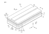
以下では、この発明の実施の形態を、添付図面を参照して詳細に説明する。
図1は、この発明の一実施形態に係る半導体レーザダイオードの構成を説明するための斜視図であり、図2は、図1のII−II線に沿う縦断面図であり、図3は、図1のIII−III線に沿う横断面図である。
この半導体レーザダイオード70は、基板1と、基板1上に結晶成長(エピタキシャル成長)によって形成されたIII族窒化物半導体積層構造2と、基板1の裏面(III族窒化物半導体積層構造2と反対側の表面)に接触するように形成されたn型電極3と、III族窒化物半導体積層構造2の表面に接触するように形成されたp型電極4とを備えたファブリペロー型のものである。
Hereinafter, embodiments of the present invention will be described in detail with reference to the accompanying drawings.
FIG. 1 is a perspective view for explaining a configuration of a semiconductor laser diode according to an embodiment of the present invention, FIG. 2 is a longitudinal sectional view taken along line II-II in FIG. 1, and FIG. It is a cross-sectional view which follows the III-III line of FIG.
The
基板1は、この実施形態では、GaN単結晶基板で構成されている。この基板1は、m面を主面としたものであり、この主面上における結晶成長によって、III族窒化物半導体積層構造2が形成されている。したがって、III族窒化物半導体積層構造2は、m面を結晶成長主面とするIII族窒化物半導体からなる。
III族窒化物半導体積層構造2は、発光層10(活性層:図2および図3において斜線を付して示す。)と、n型半導体層11と、p型半導体層12とを備えている。n型半導体層11は発光層10に対して基板1側に配置されており、p型半導体層12は発光層10に対してp型電極4側に配置されている。こうして、発光層10が、n型半導体層11およびp型半導体層12によって挟持されていて、ダブルヘテロ接合が形成されている。発光層10には、n型半導体層11から電子が注入され、p型半導体層12から正孔が注入される。これらが発光層10で再結合することにより、光が発生するようになっている。
In this embodiment, the
The group III nitride
n型半導体層11は、基板1側から順に、n型GaNコンタクト層13(たとえば2μm厚)、n型AlGaNクラッド層14(1.5μm厚以下。たとえば1.0μm厚)およびn型GaNガイド層15(たとえば0.1μm厚)を積層して構成されている。
一方、p型半導体層12は、発光層10の上に、順に、p型AlGaN電子ブロック層16(たとえば20nm厚)、およびp型GaNガイド・コンタクト層17(たとえば0.2μm厚)を積層して構成されている。
The n-
On the other hand, the p-
n型GaNコンタクト層13は、n型電極3とのオーミックコンタクトをとるための低抵抗層である。n型GaNコンタクト層13は、GaNにたとえばn型ドーパントとしてのSiを高濃度にドープ(ドーピング濃度は、たとえば、3×1018cm−3)することによってn型半導体とされている。
n型AlGaNクラッド層14は、発光層10からの光を当該発光層10側へと閉じ込める光閉じ込め効果を生じるものである。n型AlGaNクラッド層14は、AlGaNにたとえばn型ドーパントとしてのSiをドープ(ドーピング濃度は、たとえば、1×1018cm−3)することによってn型半導体とされている。n型AlGaNクラッド層14は、n型GaNガイド層15よりもバンドギャップが広い。これにより、n型AlGaNクラッド層14は、n型GaNガイド層15よりも十分に小さな屈折率を有するので、良好な閉じ込めを行うことができ、低閾値および高効率の半導体レーザダイオードを実現できる。
The n-type
The n-type
n型GaNガイド層15は、発光層10にキャリヤ(電子)を閉じ込めるためのキャリヤ閉じ込め効果を生じる半導体層である。これにより、発光層10における電子および正孔の再結合の効率が高められるようになっている。n型GaNガイド層15は、GaNにたとえばn型ドーパントとしてのSiをドープ(ドーピング濃度は、たとえば、1×1018cm−3)することによりn型半導体とされている。
The n-type
p型AlGaN電子ブロック層16は、AlGaNにp型ドーパントとしてのたとえばMgをドープ(ドーピング濃度は、たとえば、5×1018cm−3)して形成されたp型半導体であり、発光層10からの電子の流出を防いで、電子および正孔の再結合効率を高めている。
p型GaNガイド・コンタクト層17は、p型電極4とのオーミックコンタクトをとるための低抵抗層(コンタクト層)としての機能を有するとともに、発光層10にキャリヤ(正孔)を閉じ込めるためのキャリヤ閉じ込め効果を生じる半導体層としての機能をも有する層である。これにより、発光層10における電子および正孔の再結合の効率が高められるようになっている。p型GaNガイド・コンタクト層17は、GaNにたとえばp型ドーパントとしてのMgを高濃度にドープする(ドーピング濃度は、たとえば、3×1019cm−3)ことによってp型半導体とされている。p型GaNガイド・コンタクト層17は、その層厚がn型GaNガイド層15よりも大きくされており、たとえば、0.2μm厚に形成されている。
The p-type AlGaN
The p-type GaN
発光層10は、たとえばInGaNを含む多重量子井戸(MQW:Multiple-Quantum Well)構造を有しており、電子と正孔とが再結合することにより光が発生し、その発生した光を増幅させるための層である。発光層10は、具体的には、InGaN層(100Å厚以下。たとえば3nm厚)とGaN層(たとえば9nm厚)とを交互に複数周期繰り返し積層して構成されている。この場合に、InGaN層は、Inの組成比が5%以上とされることにより、バンドギャップが比較的小さくなり、量子井戸層を構成する。一方、GaN層は、バンドギャップが比較的大きなバリア層(障壁層)として機能する。たとえば、InGaN層とGaN層とは交互に2〜7周期繰り返し積層されて、MQW構造の発光層10が構成されている。発光波長は、量子井戸層(InGaN層)におけるInの組成を調整することによって、たとえば、450nm〜550nmとされている。前記MQW構造は、Inを含む量子井戸の数が3以下とされることが好ましい。
The
発光波長を460nm近傍の青色領域とするときには、量子井戸層におけるIn組成は、12%〜16%(たとえば、14%)とするとよい。また、発光波長を530nm近傍の緑色領域とするときには、量子井戸層におけるIn組成は、21%〜25%(たとえば、23%)とするとよい。
この実施形態では、p型半導体層12は、リッジ形状等に整形されておらず、その表面は平坦面となっている。この平坦な表面に接するようにp型電極4が形成されている。
When the emission wavelength is a blue region near 460 nm, the In composition in the quantum well layer is preferably 12% to 16% (for example, 14%). When the emission wavelength is in the green region near 530 nm, the In composition in the quantum well layer is preferably 21% to 25% (for example, 23%).
In this embodiment, the p-
n型電極3は、たとえば、基板1側から順にAl層、Ti層およびAu層を積層した多層構造を有しており、そのAl層が基板1にオーミック接触している。
p型電極4は、c軸方向に沿う直線形状に形成されており、p型半導体層12の表面の幅方向(a軸方向)中間部に帯状に形成されている。このp型電極4が、p型GaNガイド・コンタクト層17にオーミック接触している。p型電極4は、この実施形態ではZnO(屈折率は2.0)からなり、たとえば厚さ0.55μmの透明電極である。この透明電極からなるp型電極4は、その屈折率がn型AlGaNクラッド層14(屈折率は2.47)よりも小さく、そのため、良好な光閉じ込め効果を有する上部クラッド層として機能する。
The n-
The p-
このような構成により、p型クラッド層を設けていない構造でありながら、良好な光閉じ込め効果を得ることができ、発振効率を高めて、低閾値化に寄与することができる。また、p型半導体層12がp型クラッド層を含まない構造であるため、p型電極4から発光層10までの距離が短い。そのため、電流狭窄および横方向の光閉じ込めのためにp型半導体層12をリッジ形状に形成する必要がなく、また、電気抵抗も低くなる。しかも、Alを含むp型クラッド層を設けると、このp型クラッド層自体が高抵抗層となるが、このようなp型クラッド層を必要としない本実施形態の構成により、電気抵抗の低減を効果的に達成できる。こうして、簡単な構成でありながら、良好な発振効率を実現でき、低閾値化を実現することができる。リッジ構造を必要としない簡単な構造であるため、製造工程も簡素化できる。
With such a configuration, although the p-type cladding layer is not provided, a good light confinement effect can be obtained, and the oscillation efficiency can be increased and the threshold can be reduced. Further, since the p-
また、p型クラッドを設けていないので、n型AIGaNクラッド層14の層厚を大きく(たとえば、1.5μm以上)したり、n型クラッド層のAl組成を大きく(たとえば、8%以上)して屈折率を小さくしたりして、光閉じ込めを強く行うことが可能になる。すなわち、このようにして、も、Alを多く含むIII族窒化物半導体層の総厚が大きくならないので、クラックの発生を抑制できる。
Since no p-type cladding is provided, the layer thickness of the n-type
III族窒化物半導体積層構造2は、p型電極4の長手方向両端における劈開により形成された一対の端面21,22(劈開面)を有している。この一対の端面21,22は、互いに平行であり、いずれもc軸に垂直である。こうして、n型GaNガイド層15、発光層10およびp型GaNガイド・コンタクト層17によって、端面21,22を共振器端面とするファブリペロー共振器が形成されている。すなわち、発光層10で発生した光は、共振器端面21,22の間を往復しながら、誘導放出によって増幅される。そして、増幅された光の一部が、共振器端面21,22からレーザ光として素子外に取り出される。
The group III nitride
さらに、p型半導体層12の主面はm面であり、このm面にp型電極4が形成されている。そして、n型電極3が形成されている基板1の裏面もm面である。このように、p型電極4およびn型電極3のいずれもがm面に形成されているので、レーザの高出力化や高温動作に十分に耐えられる信頼性を実現できる。
共振器端面21,22は、それぞれ絶縁膜23,24(図1では図示を省略した。)によって被覆されている。共振器端面21は、+c軸側端面であり、共振器端面22は−c軸側端面である。すなわち、共振器端面21の結晶面は+c面であり、共振器端面22の結晶面は−c面である。−c面側の絶縁膜24は、アルカリに溶けるなど化学的に弱い−c面を保護する保護膜として機能することができ、半導体レーザダイオード70の信頼性の向上に寄与する。
Further, the main surface of the p-
The resonator end faces 21 and 22 are covered with insulating
図4に図解的に示すように、+c面である共振器端面21を被覆するように形成された絶縁膜23は、たとえばZrO2の単膜からなる。これに対し、−c面である共振器端面22に形成された絶縁膜24は、たとえばSiO2膜とZrO2膜とを交互に複数回(図4の例では5回)繰り返し積層した多重反射膜で構成されている。絶縁膜23を構成するZrO2の単膜は、その厚さがλ/2n1(ただし、λは発光層10の発光波長。n1はZrO2の屈折率)とされている。一方、絶縁膜24を構成する多重反射膜は、膜厚λ/4n2(但しn2はSiO2の屈折率)のSiO2膜と、膜厚λ/4n1のZrO2膜とを交互に積層した構造となっている。
As schematically shown in FIG. 4, the insulating
このような構造により、+c軸側端面21における反射率は小さく、−c軸側端面22における反射率が大きくなっている。より具体的には、たとえば、+c軸側端面21の反射率は20%程度とされ、−c軸側端面22における反射率は99.5%程度(ほぼ100%)となる。したがって、+c軸側端面21から、より大きなレーザ出力が出射されることになる。すなわち、この半導体レーザダイオード70では、+c軸側端面21が、レーザ出射端面とされている。
With such a structure, the reflectance at the + c-axis
このような構成によって、n型電極3およびp型電極4を電源に接続し、n型半導体層11およびp型半導体層12から電子および正孔を発光層10に注入することによって、この発光層10内で電子および正孔の再結合を生じさせ、たとえば、波長450nm〜550nmの光を発生させることができる。この光は、共振器端面21,22の間をガイド層15,17に沿って往復しながら、誘導放出によって増幅される。そして、レーザ出射端面である共振器端面21から、より多くのレーザ出力が外部に取り出されることになる。
With such a configuration, the n-
図5は、III族窒化物半導体の結晶構造のユニットセルを表した図解図である。III族窒化物半導体の結晶構造は、六方晶系で近似することができ、一つのIII族原子に対して4つの窒素原子が結合している。4つの窒素原子は、III族原子を中央に配置した正四面体の4つの頂点に位置している。これらの4つの窒素原子は、一つの窒素原子がIII族原子に対して+c軸方向に位置し、他の三つの窒素原子がIII族原子に対して−c軸側に位置している。このような構造のために、III族窒化物半導体では、分極方向がc軸に沿っている。 FIG. 5 is an illustrative view showing a unit cell of a crystal structure of a group III nitride semiconductor. The crystal structure of the group III nitride semiconductor can be approximated by a hexagonal system, and four nitrogen atoms are bonded to one group III atom. The four nitrogen atoms are located at the four vertices of a regular tetrahedron with a group III atom arranged in the center. Of these four nitrogen atoms, one nitrogen atom is located in the + c axis direction with respect to the group III atom, and the other three nitrogen atoms are located on the −c axis side with respect to the group III atom. Due to such a structure, in the group III nitride semiconductor, the polarization direction is along the c-axis.
c軸は六角柱の軸方向に沿い、このc軸を法線とする面(六角柱の頂面)がc面(0001)である。c面に平行な2つの面でIII族窒化物半導体の結晶を劈開すると、+c軸側の面(+c面)はIII族原子が並んだ結晶面となり、−c軸側の面(−c面)は窒素原子が並んだ結晶面となる。そのため、c面は、+c軸側と−c軸側とで異なる性質を示すので、極性面(Polar Plane)と呼ばれる。 The c-axis is along the axial direction of the hexagonal column, and the surface (the top surface of the hexagonal column) having the c-axis as a normal is the c-plane (0001). When a group III nitride semiconductor crystal is cleaved by two planes parallel to the c-plane, the + c-axis side plane (+ c plane) becomes a crystal plane in which group III atoms are arranged, and the −c-axis side plane (−c plane) ) Is a crystal plane with nitrogen atoms. For this reason, the c-plane is called a polar plane because it exhibits different properties on the + c-axis side and the −c-axis side.
+c面と−c面とは異なる結晶面であるので、それに応じて、異なる物性を示す。具体的には、+c面は、アルカリに強いなどといった化学反応性に対する耐久性が高い性質を示し、逆に、−c面は化学的に弱く、たとえば、アルカリに溶けてしまうことが分かっている。
一方、六角柱の側面がそれぞれm面(10-10)であり、隣り合わない一対の稜線を通る面がa面(11-20)である。これらは、c面に対して直角な結晶面であり、分極方向に対して直交しているため、極性のない平面、すなわち、非極性面(Nonpolar Plane)である。さらに、c面に対して傾斜している(平行でもなく直角でもない)結晶面は、分極方向に対して斜めに交差しているため、若干の極性のある平面、すなわち、半極性面(Semipolar Plane)である。半極性面の具体例は、(10-1-1)面、(10-1-3)面、(11-22)面などの面である。
Since the + c plane and the −c plane are different crystal planes, different physical properties are exhibited accordingly. Specifically, it is known that the + c surface exhibits a high durability against chemical reactivity such as being strong against alkali, and conversely, the -c surface is chemically weak and, for example, is soluble in alkali. .
On the other hand, the side surfaces of the hexagonal columns are m-planes (10-10), respectively, and the plane passing through a pair of ridge lines that are not adjacent to each other is the a-plane (11-20). Since these are crystal planes perpendicular to the c-plane and orthogonal to the polarization direction, they are nonpolar planes, that is, nonpolar planes. Furthermore, since the crystal plane inclined with respect to the c-plane (not parallel nor perpendicular) intersects the polarization direction obliquely, it has a slightly polar plane, that is, a semipolar plane (Semipolar plane). Plane). Specific examples of the semipolar plane include planes such as the (10-1-1) plane, the (10-1-3) plane, and the (11-22) plane.
非特許文献1に、c面に対する結晶面の偏角と当該結晶面の法線方向の分極との関係が示されている。この非特許文献1から、(11-24)面、(10-12)面なども分極の少ない結晶面であり、大きな偏光状態の光を取り出すために採用される可能性のある有力な結晶面であると言える。
たとえば、m面を主面とするGaN単結晶基板は、c面を主面としたGaN単結晶から切り出して作製することができる。切り出された基板のm面は、たとえば、化学的機械的研磨処理によって研磨され、(0001)方向および(11−20)方向の両方に関する方位誤差(オフ角)が、±1°以内(好ましくは±0.3°以内)とされる。こうして、m面を主面とし、かつ、転位や積層欠陥といった結晶欠陥のないGaN単結晶基板が得られる。このようなGaN単結晶基板の表面には、原子レベルの段差が生じているにすぎない。
For example, a GaN single crystal substrate having an m-plane as a main surface can be produced by cutting from a GaN single crystal having a c-plane as a main surface. The m-plane of the cut substrate is polished by, for example, a chemical mechanical polishing process, and the azimuth error (off angle) in both the (0001) direction and the (11-20) direction is within ± 1 ° (preferably Within ± 0.3 °). In this way, a GaN single crystal substrate having the m-plane as the main surface and free from crystal defects such as dislocations and stacking faults can be obtained. There is only an atomic level step on the surface of such a GaN single crystal substrate.
このようにして得られるGaN単結晶基板上に、有機金属気相成長法によって、半導体レーザダイオード構造を構成するIII族窒化物半導体積層構造2が成長させられる。
m面を主面とするGaN単結晶基板1上にm面を成長主面とするIII族窒化物半導体積層構造2を成長させてa面に沿う断面を電子顕微鏡(STEM:走査透過電子顕微鏡)で観察すると、III族窒化物半導体積層構造2には、転位の存在を表す条線が見られない。そして、表面状態を光学顕微鏡で観察すると、c軸方向への平坦性(最高部と最低部との高さの差)は10Å以下であることが分かる。このことは、発光層10、とくに量子井戸層のc軸方向への平坦性が10Å以下であることを意味し、発光スペクトルの半値幅を低くすることができる。
The group III nitride
A group III nitride
このように、無転位でかつ積層界面が平坦なm面III族窒化物半導体を成長させることができる。ただし、GaN単結晶基板1の主面のオフ角は±1°以内(好ましくは±0.3°以内)とすることが好ましく、たとえば、オフ角を2°としたm面GaN単結晶基板上にGaN半導体層を成長させると、GaN結晶がテラス状に成長し、オフ角を±1°以内とした場合のような平坦な表面状態とすることができないおそれがある。
Thus, an m-plane group III nitride semiconductor having no dislocation and a flat stacked interface can be grown. However, the off angle of the main surface of the GaN
m面を主面としたGaN単結晶基板上に結晶成長させられるIII族窒化物半導体は、m面を成長主面として成長する。c面を主面として結晶成長した場合には、c軸方向の分極の影響で、発光層10での発光効率が悪くなるおそれがある。これに対して、m面を結晶成長主面とすれば、量子井戸層での分極が抑制され、発光効率が増加する。これにより、閾値の低下やスロープ効率の増加を実現できる。また、分極が少ないため、発光波長の電流依存性が抑制され、安定した発振波長を実現できる。
A group III nitride semiconductor crystal grown on a GaN single crystal substrate having an m-plane as a main surface grows with the m-plane as a main growth surface. When the crystal growth is performed with the c-plane as the main surface, the light-emitting efficiency in the light-emitting
また、m面を結晶成長の主面とすることにより、III族窒化物半導体結晶の成長を極めて安定に行うことができ、c面やa面を結晶成長主面とする場合よりも、結晶性を向上することができる。これにより、高性能のレーザダイオードの作製が可能になる。
発光層10は、m面を結晶成長主面として成長させられたIII族窒化物半導体からなるので、ここから発生する光は、a軸方向、すなわちm面に平行な方向に偏光しており、TEモードの場合、その進行方向はc軸方向である。いいかえると、a軸方向に偏光したa面内方向へ出射する光子の割合が多いので、横方向の閉じ込めをしなくても、自ずとc軸方向に伝搬する光の割合が多い。したがって、半導体レーザダイオード70は、結晶成長主面が偏光方向に平行であり、かつ、ストライプ方向、すなわち導波路の方向が光の進行方向と平行に設定されている。これにより、TEモードの発振を容易に生じさせることができ、レーザ発振を生じさせるための閾値電流を低減することができる。
Further, by making the m-plane the main surface for crystal growth, the group III nitride semiconductor crystal can be grown extremely stably, and the crystallinity is higher than when the c-plane and the a-plane are used as the main crystal growth surface. Can be improved. As a result, a high-performance laser diode can be manufactured.
Since the
換言すれば、m面を結晶成長の主面とすることにより、c軸方向とa軸方向とに物性の異方性が生じる。さらに、Inを含む発光層10は、格子歪みによる2軸性応力によって、c面を結晶成長の主面とした場合とは異なる量子井戸バンド構造が生じる。その結果、c面を結晶成長の主面としたIII族窒化物半導体の場合とは異なる利得が得られ、それにより、レーザ特性を向上することができる。
In other words, anisotropy of physical properties occurs in the c-axis direction and the a-axis direction by using the m-plane as the main surface for crystal growth. Further, the light-emitting
また、この実施形態では、基板1としてGaN単結晶基板を用いているので、III族窒化物半導体積層構造2は、欠陥の少ない高い結晶品質を有することができる。その結果、高性能のレーザダイオードを実現できる。
さらにまた、実質的に転位のないGaN単結晶基板上にIII族窒化物半導体積層構造を成長させることにより、このIII族窒化物半導体積層構造2は基板1の成長面(m面)からの積層欠陥や貫通転位が生じていない良好な結晶とすることができる。これにより、欠陥に起因する発光効率低下などの特性劣化を抑制することができる。
In this embodiment, since the GaN single crystal substrate is used as the
Furthermore, by growing a group III nitride semiconductor multilayer structure on a GaN single crystal substrate substantially free of dislocations, this group III nitride
図6は、光閉じ込めの状態を説明するための図であり、半導体レーザダイオードを構成する各層の屈折率(refractive index)と、素子厚さ(Y)方向各位置の光強度(Optical Intensity)の分布とが示されている。
図6(a)は、p型半導体層中にp型クラッド層を有する従来技術(図10参照)に係る半導体レーザダイオードの各層の屈折率、および素子厚さ方向の光強度分布を示す。発光層に関してn型層およびp型層の組成および層厚が対称に形成されている結果、発光層と光強度のピーク位置とが整合している。
FIG. 6 is a diagram for explaining the state of optical confinement. The refractive index (refractive index) of each layer constituting the semiconductor laser diode and the light intensity (Optical Intensity) at each position in the element thickness (Y) direction are shown. Distribution is shown.
FIG. 6A shows the refractive index of each layer of the semiconductor laser diode according to the prior art (see FIG. 10) having a p-type cladding layer in the p-type semiconductor layer, and the light intensity distribution in the element thickness direction. As a result of the composition and layer thickness of the n-type layer and the p-type layer being symmetrical with respect to the light emitting layer, the light emitting layer and the peak position of the light intensity are matched.
図6(b)は、図1等に示した構造の半導体レーザダイオード70において、p型GaNガイド・コンタクト層17の層厚とn型GaNガイド層15の層厚とを等しくした場合の各層の屈折率および素子厚さ方向の光強度分布とを示す。上部クラッド層としてのp型電極4(ZnOからなる透明電極)の屈折率は2.0程度であり、n型AlGaNクラッド層14の屈折率よりも低い。そのため、発光層10の上下で屈折率のバランスが対称ではなく、それに応じて光強度のピーク位置は、発光層10よりもn型AlGaNクラッド層14側にシフトしている。
FIG. 6B shows a
図6(c)は、この実施形態に係る半導体レーザダイオード70における各層の屈折率および素子厚さ方向の光強度分布を示す。p型GaNガイド・コンタクト層17の層厚は、n型AlGaNクラッド層14よりも厚く(この例では100nmだけ厚く)形成されており、これにより、光強度のピーク位置が発光層10に整合している。すなわち、光強度のピーク位置が発光層10の位置と整合するように、p型GaNガイド・コンタクト層17の層厚が調整されている。これにより、発光層10に効率的に光を閉じ込めることができるので、発振効率が高まり、低閾値化が達成されている。
FIG. 6C shows the refractive index of each layer and the light intensity distribution in the element thickness direction in the
図7は、III族窒化物半導体積層構造2を構成する各層を成長させるための処理装置の構成を説明するための図解図である。処理室30内に、ヒータ31を内蔵したサセプタ32が配置されている。サセプタ32は、回転軸33に結合されており、この回転軸33は、処理室30外に配置された回転駆動機構34によって回転されるようになっている。これにより、サセプタ32に処理対象のウエハ35を保持させることにより、処理室30内でウエハ35を所定温度に昇温することができ、かつ、回転させることができる。ウエハ35は、前述のGaN単結晶基板1を構成するGaN単結晶ウエハである。
FIG. 7 is an illustrative view for illustrating the configuration of a processing apparatus for growing each layer constituting group III nitride
処理室30には、排気配管36が接続されている。排気配管36はロータリポンプ等の排気設備に接続されている。これにより、処理室30内の圧力は、1/10気圧〜常圧とされ、処理室30内の雰囲気は常時排気されている。
一方、処理室30には、サセプタ32に保持されたウエハ35の表面に向けて原料ガスを供給するための原料ガス供給路40が導入されている。この原料ガス供給路40には、窒素原料ガスとしてのアンモニアを供給する窒素原料配管41と、ガリウム原料ガスとしてのトリメチルガリウム(TMG)を供給するガリウム原料配管42と、アルミニウム原料ガスとしてのトリメチルアルミニウム(TMAl)を供給するアルミニウム原料配管43と、インジウム原料ガスとしてのトリメチルインジウム(TMIn)を供給するインジウム原料配管44と、マグネシウム原料ガスとしてのエチルシクロペンタジエニルマグネシウム(EtCp2Mg)を供給するマグネシウム原料配管45と、シリコンの原料ガスとしてのシラン(SiH4)を供給するシリコン原料配管46とが接続されている。これらの原料配管41〜46には、それぞれバルブ51〜56が介装されている。各原料ガスは、いずれも水素もしくは窒素またはこれらの両方からなるキャリヤガスとともに供給されるようになっている。
An
On the other hand, a raw material
たとえば、m面を主面とするGaN単結晶ウエハをウエハ35としてサセプタ32に保持させる。この状態で、バルブ52〜56は閉じておき、窒素原料バルブ51を開いて、処理室30内に、キャリヤガスおよびアンモニアガス(窒素原料ガス)が供給される。さらに、ヒータ31への通電が行われ、ウエハ温度が1000℃〜1100℃(たとえば、1050℃)まで昇温される。これにより、表面の荒れを生じさせることなくIII族窒化物半導体を成長させることができるようになる。
For example, a GaN single crystal wafer having an m-plane as a main surface is held on the
ウエハ温度が1000℃〜1100℃に達するまで待機した後、窒素原料バルブ51、ガリウム原料バルブ52およびシリコン原料バルブ56が開かれる。これにより、原料ガス供給路40から、キャリヤガスとともに、アンモニア、トリメチルガリウムおよびシランが供給される。その結果、ウエハ35の表面に、シリコンがドープされたGaN層からなるn型GaNコンタクト層13が成長する。
After waiting until the wafer temperature reaches 1000 ° C. to 1100 ° C., the
続いて、窒素原料バルブ51、ガリウム原料バルブ52およびシリコン原料バルブ56を開いた状態で、さらにアルミニウム原料バルブ53が開かれる。これにより、原料ガス供給路40から、キャリヤガスとともに、アンモニア、トリメチルガリウム、シランおよびトリメチルアルミニウムが供給される。その結果、n型GaNコンタクト層13上に、n型AlGaNクラッド層14がエピタキシャル成長させられる。
Subsequently, the
次いで、窒素原料バルブ51、ガリウム原料バルブ52およびシリコン原料バルブ56を開いた状態で、アルミニウム原料バルブ53を閉じる。これにより、原料ガス供給路40から、キャリヤガスとともに、アンモニア、トリメチルガリウムおよびシランが供給される。その結果、n型AlGaNクラッド層14上にn型GaNガイド層15がエピタキシャル成長させられる。n型GaNガイド層15の形成時には、ウエハ35の温度は、800℃〜900℃(たとえば850℃)とされることが好ましい。
Next, the
次に、シリコン原料バルブ56が閉じられ、多重量子井戸構造の発光層10(活性層)の成長が行われる。発光層10の成長は、たとえば、窒素原料バルブ51、ガリウム原料バルブ52およびインジウム原料バルブ54を開いてアンモニア、トリメチルガリウムおよびトリメチルインジウムをウエハ35へと供給することによりInGaN層(量子井戸層)を成長させる工程と、インジウム原料バルブ54を閉じ、窒素原料バルブ51およびガリウム原料バルブ52を開いてアンモニアおよびトリメチルガリウムをウエハ35へと供給することにより、無添加のGaN層(バリア層)を成長させる工程とを交互に実行することによって行える。たとえば、GaN層を始めに形成し、その上にInGaN層を形成する。これを、たとえば、5回に渡って繰り返し行う。発光層10の形成時には、ウエハ35の温度は、たとえば、700℃〜800℃(たとえば730℃)とされることが好ましい。このとき、成長圧力は700torr以上とすることが好ましく、これにより、耐熱性を向上することができる。InGaN層(量子井戸層)のIn組成は、前述のとおり、発光波長に応じて調整される。
Next, the
次いで、p型AlGaN電子ブロック層16が形成される。すなわち、窒素原料バルブ51、ガリウム原料バルブ52、アルミニウム原料バルブ53およびマグネシウム原料バルブ55が開かれ、他のバルブ54,56が閉じられる。これにより、ウエハ35に向けて、アンモニア、トリメチルガリウム、トリメチルアルミニウムおよびエチルシクロペンタジエニルマグネシウムが供給され、マグネシウムがドープされたAlGaN層からなるp型電子ブロック層16が形成されることになる。このp型電子ブロック層16の形成時には、ウエハ35の温度は、1000℃〜1100℃(たとえば1000℃)とされることが好ましい。
Next, the p-type AlGaN
次に、アルミニウム原料バルブ53が閉じられ、窒素原料バルブ51、ガリウム原料バルブ52およびマグネシウム原料バルブ55が開かれる。これにより、ウエハ35に向けて、アンモニア、トリメチルガリウムおよびエチルシクロペンタジエニルマグネシウムが供給され、マグネシウムがドープされたp型GaN層からなるp型GaNガイド・コンタクト層17が形成されることになる。このp型GaNガイド・コンタクト層17の形成時には、ウエハ35の温度は、800℃〜900℃(たとえば850℃)とされることが好ましい。
Next, the
ウエハ35(GaN単結晶基板1)上にIII族窒化物半導体積層構造2の構成層10,13〜17を成長するのに際しては、いずれの層の成長の際も、処理室30内のウエハ35に供給されるガリウム原料(トリメチルガリウム)のモル分率に対する窒素原料(アンモニア)のモル分率の比であるV/III比は、1000以上(好ましくは3000以上)の高い値に維持される。より具体的には、n型クラッド層14から最上層のp型GaNガイド・コンタクト層17までの成長過程において、V/III比の平均値が1000以上であることが好ましい。これにより、n型クラッド層14からp型GaNガイド・コンタクト層17までの全ての層において、点欠陥の少ない良好な結晶を得ることができる。
When the
この実施形態では、上記のような高いV/III比を用い、かつ、GaN単結晶基板1とIII族窒化物半導体積層構造2との間にバッファ層を介在することなく、m面等を主面とするIII族窒化物半導体積層構造2が、無転位の状態で、かつ、平坦に成長する。このIII族窒化物半導体積層構造2は、GaN単結晶基板1の主面から生じる積層欠陥や貫通転位を有していない。
In this embodiment, an m-plane or the like is mainly used without using a buffer layer between the GaN
こうして、ウエハ35上にIII族窒化物半導体積層構造2が成長させられると、次に、p型GaNガイド・コンタクト層17にオーミック接触するp型電極4が形成され、n型GaNコンタクト層13にオーミック接触するn型電極3が形成される。n型電極3の形成は、たとえば、抵抗加熱または電子線ビームによる金属蒸着装置によって行うことができる。また、p型電極4の形成は、たとえば、スパッタ法で行うことができる。p型電極4をc軸方向に沿う直線帯状パターンに形成するために、p型GaNガイド・コンタクト層17の表面に予めフォトレジスト膜のパターンを形成しておく。このフォトレジスト膜は、p型電極4に対応する直線帯状の開口を有するパターンに形成される。その後、p型電極4の材料膜を堆積し、この材料膜をフォトレジスト膜とともにリフトオフすることによって、c軸方向に沿う直線帯状のp型電極4を形成できる。
Thus, when the group III nitride
次の工程は、個別素子への分割である。すなわち、ウエハ35をp型電極4に平行な方向である共振器方向に平行な方向およびこれに垂直な方向に劈開して、半導体レーザダイオードを構成する個々の素子が切り出される。共振器方向に平行な方向に関する分割はa面に沿って行われる。また、共振器方向に垂直な方向に関する分割はc面に沿う劈開によって行われる。このc面に沿う劈開によって、+c面(劈開面)からなる共振器端面21と、−c面(劈開面)からなる共振器端面22とが形成される。
The next step is a division into individual elements. That is, the
共振器端面21,22には、それぞれ前述の絶縁膜23,24が形成される。この絶縁膜23,24の形成は、たとえば、電子サイクロトロン共鳴(ECR)成膜法によって行うことができる。共振器方向に垂直な方向に関するウエハ分割(c面に沿う劈開)を行ってバー状体を形成し、このバー状体の側面(c面)に絶縁膜23,24を形成し、その後に、バー状体をa面に沿って分割するとよい。これにより、絶縁膜23,24の形成工程を複数のチップに関して共通に行うことができる。
The above-described
図8は、この発明の第2の実施形態に係る半導体レーザダイオードの構成を説明するための横断面図である。この図8において、前述の第1の実施形態の半導体レーザダイオードの各部に対応する部分には同一の参照符号を付して示す。この実施形態の半導体レーザダイオード71では、p型GaNガイド・コンタクト層17は、発光層10側の第1層17Aと、p型電極4側の第2層17Bとを有する2層構造に形成されている。第1層17Aはp型AlGaN電子ブロック層16に接しており、第2層17Bはp型電極4に接している。第1層17Aはp型不純物であるMgの濃度は比較的低く(たとえば1015cm−3〜1019cm−3)されており、第2層17Bはp型不純物であるMgの濃度が比較的高く(たとえば1019cm−3〜1020cm−3)されている。
FIG. 8 is a cross-sectional view for explaining the structure of a semiconductor laser diode according to the second embodiment of the present invention. In FIG. 8, portions corresponding to the respective portions of the semiconductor laser diode of the first embodiment are denoted by the same reference numerals. In the
発光層10に近い第1層17AのMg濃度が低いので、Mgに起因する光吸収を低減できる。一方、p型電極4側の第2層17BのMg濃度が高いので、p型電極4とp型GaNガイド・コンタクト層17との間に良好なオーミック接触を形成できる。これにより、より一層発振効率を高めることができるので、閾値電流を低減できる。
p型GaNガイド・コンタクト層17は、3層以上のp型GaN層を有する構成とすることもできる。この場合、p型AlGaN電子ブロック層16に接する層のp型不純物濃度を低くし、p型電極4に接する層のp型不純物濃度を高くすることが好ましい。
Since the Mg concentration of the
The p-type GaN
また、p型GaNガイド・コンタクト層17が明確に複数の層を有する必要はなく、たとえば、p型AlGaN電子ブロック層16からp型電極4に向かうに従ってp型不純物濃度が漸増するp型半導体層によってp型ガイド・コンタクト層17を構成してもよい。
図9は、この発明の第2の実施形態に係る半導体レーザダイオードの構成を示す横断面である。この図9において、前述の第1の実施形態の半導体レーザダイオード70の各部に対応する部分には同一の参照符号を付して示す。
Further, the p-type GaN
FIG. 9 is a cross section showing a configuration of a semiconductor laser diode according to the second embodiment of the present invention. In FIG. 9, portions corresponding to the respective portions of the
この実施形態の半導体レーザダイオード72は、p型GaNガイド・コンタクト層17の表面において、p型電極4との接触部以外の領域が、絶縁膜6で被われている。この絶縁膜6は、p型GaNガイド・コンタクト層17よりも屈折率の小さい材料、たとえば、酸化シリコン(SiO2:屈折率は1.5)または酸化ジルコニウム(ZrO2:屈折率は2.1)からなる。p型電極4は、絶縁膜6に形成された開口6aにおいて、p型GaNガイド・コンタクト層17の表面に接し、当該絶縁膜6の表面を覆っている。開口6aは、c軸方向に沿う直線帯状に形成されており、素子の幅方向(a軸方向)中間部に形成されている。したがって、p型電極4は、第1の実施形態の場合と同様な直線帯状領域でp型GaNガイド・コンタクト層17の表面にオーミック接触している。
In the
このような構成により、絶縁膜6において電流狭窄を行うことができるとともに、上部クラッド層としてのp型電極4とともに絶縁膜6が発光層10への光閉じ込めに寄与する。これにより、一層効率的な光閉じ込めを行うことができるので、発振効率を一層向上して、低閾値化を図ることができる。
絶縁膜6の形成は、たとえば、リフトオフ工程を用いて行われる。すなわち、p型GaNガイド・コンタクト層17の表面にストライプ状のマスクを形成した後、p型GaNガイド・コンタクト層17の表面全体を覆うように絶縁体薄膜を形成する。その後、この絶縁体薄膜をリフトオフしてp型GaNガイド・コンタクト層17を露出させるようにして、絶縁膜6を形成できる。
With such a configuration, current can be confined in the insulating
The insulating
次いで、p型GaNガイド・コンタクト層17にオーミック接触するp型電極4が絶縁膜6を覆うように形成される。
以上、この発明の3つの実施形態について説明したが、この発明はさらに他の形態で実施することもできる。たとえば、III族窒化物半導体積層構造2を構成する各層の層厚や不純物濃度等は一例であり、適宜適切な値を選択して用いることができる。また、n型クラッド層14は、必ずしもAlGaNの単層である必要はなく、AlGaN層とGaN層とで構成された超格子層としてもよい。
Next, the p-
Although three embodiments of the present invention have been described above, the present invention can be implemented in other forms. For example, the layer thickness, impurity concentration, and the like of each layer constituting the group III nitride
また、前述の実施形態では、III族窒化物半導体積層構造2がm面を成長主面としており、共振器方向がc軸方向とされているが、共振器方向をa軸方向にとってもよい。また、a面またはを成長主面としたIII族窒化物半導体積層構造で同様なレーザ構造を形成する場合にも、この発明を適用することができる。
さらに、III族窒化物半導体積層構造2を形成した後にレーザリフトオフなどで基板1を除去し、基板1のない半導体レーザダイオードとすることもできる。
In the above-described embodiment, the group III nitride
Further, after forming the group III nitride
その他、特許請求の範囲に記載された事項の範囲で種々の設計変更を施すことが可能である。 In addition, various design changes can be made within the scope of matters described in the claims.
1 基板
2 III族窒化物半導体積層構造
3 n型電極
4 p型電極
6 絶縁膜
6a 開口
10 発光層
11 n型半導体層
12 p型半導体層
13 p型GaNコンタクト層
14 n型AlGaNクラッド層
15 n型GaNガイド層
16 p型AlGaN電子ブロック層
17 p型GaNガイド・コンタクト層
17A 第1層
17B 第2層
21,22 共振器端面
23,24 絶縁膜
30 処理室
31 ヒータ
32 サセプタ
33 回転軸
34 回転駆動機構
35 ウエハ
36 排気配管
40 原料ガス供給路
41 窒素原料配管
42 ガリウム原料配管
43 アルミニウム原料配管
44 インジウム原料配管
45 マグネシウム原料配管
46 シリコン原料配管
51 窒素原料バルブ
52 ガリウム原料バルブ
53 アルミニウム原料バルブ
54 インジウム原料バルブ
55 マグネシウム原料バルブ
56 シリコン原料バルブ
70,71,72 半導体レーザダイオード
DESCRIPTION OF
Claims (3)
前記p型半導体層上に形成され、前記n型クラッド層よりも屈折率の小さい透明電極からなる上部クラッド層と、を含む、半導体レーザダイオード。 From an n-type cladding layer, an n-type guide layer formed on the n-type cladding layer, a light-emitting layer containing In formed on the n-type guide layer, and the n-type guide layer formed on the light-emitting layer A group III nitride semiconductor multilayer structure including a p-type semiconductor layer having a large layer thickness;
A semiconductor laser diode comprising: an upper clad layer formed on the p-type semiconductor layer and made of a transparent electrode having a refractive index smaller than that of the n-type clad layer.
前記第1の層のp型不純物濃度が、前記第2の層のp型不純物濃度よりも低い、請求項1または2に記載の半導体レーザダイオード。 The p-type semiconductor layer includes a first layer relatively disposed near the light emitting layer, and a second layer relatively disposed near the upper cladding layer,
3. The semiconductor laser diode according to claim 1, wherein a p-type impurity concentration of the first layer is lower than a p-type impurity concentration of the second layer.
Priority Applications (1)
| Application Number | Priority Date | Filing Date | Title |
|---|---|---|---|
| JP2007264790A JP2009094360A (en) | 2007-10-10 | 2007-10-10 | Semiconductor laser diode |
Applications Claiming Priority (1)
| Application Number | Priority Date | Filing Date | Title |
|---|---|---|---|
| JP2007264790A JP2009094360A (en) | 2007-10-10 | 2007-10-10 | Semiconductor laser diode |
Publications (1)
| Publication Number | Publication Date |
|---|---|
| JP2009094360A true JP2009094360A (en) | 2009-04-30 |
Family
ID=40666030
Family Applications (1)
| Application Number | Title | Priority Date | Filing Date |
|---|---|---|---|
| JP2007264790A Pending JP2009094360A (en) | 2007-10-10 | 2007-10-10 | Semiconductor laser diode |
Country Status (1)
| Country | Link |
|---|---|
| JP (1) | JP2009094360A (en) |
Cited By (16)
| Publication number | Priority date | Publication date | Assignee | Title |
|---|---|---|---|---|
| JP2010263163A (en) * | 2009-05-11 | 2010-11-18 | Sumitomo Electric Ind Ltd | Nitride semiconductor light-emitting element |
| CN101944480A (en) * | 2009-07-02 | 2011-01-12 | 夏普株式会社 | Nitride semiconductor chip and manufacture method thereof and semiconductor device |
| JP2011014746A (en) * | 2009-07-02 | 2011-01-20 | Sharp Corp | Nitride semiconductor element, method of fabricating the same, and semiconductor device |
| JP2011018784A (en) * | 2009-07-09 | 2011-01-27 | Sony Corp | Semiconductor laser element, driving method thereof, and semiconductor laser device |
| JP2011029237A (en) * | 2009-07-21 | 2011-02-10 | Sharp Corp | Nitride semiconductor chip, method of fabrication thereof, and semiconductor device |
| JP2012094896A (en) * | 2012-01-11 | 2012-05-17 | Sumitomo Electric Ind Ltd | Nitride-based semiconductor light-emitting element |
| US8344413B2 (en) | 2009-05-29 | 2013-01-01 | Sharp Kabushiki Kaisha | Nitride semiconductor wafer, nitride semiconductor chip, and method of manufacture of nitride semiconductor chip |
| US8664688B2 (en) | 2009-03-27 | 2014-03-04 | Sharp Kabushiki Kaisha | Nitride semiconductor light-emitting chip, method of manufacture thereof, and semiconductor optical device |
| US8748868B2 (en) | 2009-05-11 | 2014-06-10 | Sumitomo Electric Industries, Ltd. | Nitride semiconductor light emitting device and epitaxial substrate |
| US8885681B2 (en) | 2011-07-14 | 2014-11-11 | Rohm Co., Ltd. | Semiconductor laser device |
| JP2015220323A (en) * | 2014-05-16 | 2015-12-07 | 日本電信電話株式会社 | Semiconductor optical device |
| JP2018517295A (en) * | 2015-05-19 | 2018-06-28 | イェール ユニバーシティーYale University | Method and device for high confinement factor III-nitride edge emitting laser diode with lattice matched cladding layer |
| US11018231B2 (en) | 2014-12-01 | 2021-05-25 | Yale University | Method to make buried, highly conductive p-type III-nitride layers |
| US11043792B2 (en) | 2014-09-30 | 2021-06-22 | Yale University | Method for GaN vertical microcavity surface emitting laser (VCSEL) |
| US11095096B2 (en) | 2014-04-16 | 2021-08-17 | Yale University | Method for a GaN vertical microcavity surface emitting laser (VCSEL) |
| US11271368B2 (en) | 2018-01-23 | 2022-03-08 | Sony Semiconductor Solutions Corporation | Semiconductor laser and electronic apparatus |
Citations (3)
| Publication number | Priority date | Publication date | Assignee | Title |
|---|---|---|---|---|
| JP2003163418A (en) * | 2001-11-29 | 2003-06-06 | Nichia Chem Ind Ltd | Nitride gallium system compound semiconductor laser |
| JP2004289157A (en) * | 2003-03-20 | 2004-10-14 | Xerox Corp | Laser diode structure and manufacturing method thereof |
| WO2007052628A1 (en) * | 2005-10-31 | 2007-05-10 | Nichia Corporation | Nitride semiconductor element |
-
2007
- 2007-10-10 JP JP2007264790A patent/JP2009094360A/en active Pending
Patent Citations (3)
| Publication number | Priority date | Publication date | Assignee | Title |
|---|---|---|---|---|
| JP2003163418A (en) * | 2001-11-29 | 2003-06-06 | Nichia Chem Ind Ltd | Nitride gallium system compound semiconductor laser |
| JP2004289157A (en) * | 2003-03-20 | 2004-10-14 | Xerox Corp | Laser diode structure and manufacturing method thereof |
| WO2007052628A1 (en) * | 2005-10-31 | 2007-05-10 | Nichia Corporation | Nitride semiconductor element |
Cited By (19)
| Publication number | Priority date | Publication date | Assignee | Title |
|---|---|---|---|---|
| US8664688B2 (en) | 2009-03-27 | 2014-03-04 | Sharp Kabushiki Kaisha | Nitride semiconductor light-emitting chip, method of manufacture thereof, and semiconductor optical device |
| US8748868B2 (en) | 2009-05-11 | 2014-06-10 | Sumitomo Electric Industries, Ltd. | Nitride semiconductor light emitting device and epitaxial substrate |
| JP2010263163A (en) * | 2009-05-11 | 2010-11-18 | Sumitomo Electric Ind Ltd | Nitride semiconductor light-emitting element |
| US8513684B2 (en) | 2009-05-11 | 2013-08-20 | Sumitomo Electric Industries, Ltd. | Nitride semiconductor light emitting device |
| US8344413B2 (en) | 2009-05-29 | 2013-01-01 | Sharp Kabushiki Kaisha | Nitride semiconductor wafer, nitride semiconductor chip, and method of manufacture of nitride semiconductor chip |
| CN101944480A (en) * | 2009-07-02 | 2011-01-12 | 夏普株式会社 | Nitride semiconductor chip and manufacture method thereof and semiconductor device |
| JP2011014746A (en) * | 2009-07-02 | 2011-01-20 | Sharp Corp | Nitride semiconductor element, method of fabricating the same, and semiconductor device |
| JP2011018784A (en) * | 2009-07-09 | 2011-01-27 | Sony Corp | Semiconductor laser element, driving method thereof, and semiconductor laser device |
| US8989228B2 (en) | 2009-07-09 | 2015-03-24 | Sony Corporation | Laser diode device, method of driving the same, and laser diode apparatus |
| JP2011029237A (en) * | 2009-07-21 | 2011-02-10 | Sharp Corp | Nitride semiconductor chip, method of fabrication thereof, and semiconductor device |
| US8885681B2 (en) | 2011-07-14 | 2014-11-11 | Rohm Co., Ltd. | Semiconductor laser device |
| US9444225B2 (en) | 2011-07-14 | 2016-09-13 | Rohm Co., Ltd. | Semiconductor laser device |
| JP2012094896A (en) * | 2012-01-11 | 2012-05-17 | Sumitomo Electric Ind Ltd | Nitride-based semiconductor light-emitting element |
| US11095096B2 (en) | 2014-04-16 | 2021-08-17 | Yale University | Method for a GaN vertical microcavity surface emitting laser (VCSEL) |
| JP2015220323A (en) * | 2014-05-16 | 2015-12-07 | 日本電信電話株式会社 | Semiconductor optical device |
| US11043792B2 (en) | 2014-09-30 | 2021-06-22 | Yale University | Method for GaN vertical microcavity surface emitting laser (VCSEL) |
| US11018231B2 (en) | 2014-12-01 | 2021-05-25 | Yale University | Method to make buried, highly conductive p-type III-nitride layers |
| JP2018517295A (en) * | 2015-05-19 | 2018-06-28 | イェール ユニバーシティーYale University | Method and device for high confinement factor III-nitride edge emitting laser diode with lattice matched cladding layer |
| US11271368B2 (en) | 2018-01-23 | 2022-03-08 | Sony Semiconductor Solutions Corporation | Semiconductor laser and electronic apparatus |
Similar Documents
| Publication | Publication Date | Title |
|---|---|---|
| JP5118392B2 (en) | Semiconductor light emitting device and manufacturing method thereof | |
| US7792171B2 (en) | Nitride semiconductor laser device | |
| JP2009094360A (en) | Semiconductor laser diode | |
| US7843980B2 (en) | Semiconductor laser diode | |
| JP2008198952A (en) | Group iii nitride semiconductor light emitting device | |
| JP2010177651A (en) | Semiconductor laser device | |
| US8017932B2 (en) | Light-emitting device | |
| US8432946B2 (en) | Nitride semiconductor laser diode | |
| JP2009252861A (en) | Semiconductor laser device | |
| JP2009081374A (en) | Semiconductor light-emitting device | |
| US20090238227A1 (en) | Semiconductor light emitting device | |
| JP2008187044A (en) | Semiconductor laser | |
| KR100705886B1 (en) | Nitride semiconductor layer structure and a nitride semiconductor laser incorporating a portion of same | |
| JP5444609B2 (en) | Semiconductor laser element | |
| JP2011003661A (en) | Semiconductor laser element | |
| JP2008226865A (en) | Semiconductor laser diode | |
| JP5158834B2 (en) | Semiconductor light emitting device and method for manufacturing semiconductor light emitting device | |
| JP5223531B2 (en) | Semiconductor laser element | |
| JP5224312B2 (en) | Semiconductor laser diode | |
| JP2009239084A (en) | Semiconductor laser element | |
| JP2008235803A (en) | Nitride semiconductor light-emitting element | |
| JP2009246005A (en) | Semiconductor light emitting device | |
| JP2009212343A (en) | Nitride semiconductor element, and method of manufacturing the same | |
| JP2009164234A (en) | Nitride semiconductor laser device | |
| JP2009239083A (en) | Semiconductor light-emitting element |
Legal Events
| Date | Code | Title | Description |
|---|---|---|---|
| A621 | Written request for application examination |
Effective date: 20101008 Free format text: JAPANESE INTERMEDIATE CODE: A621 |
|
| A977 | Report on retrieval |
Free format text: JAPANESE INTERMEDIATE CODE: A971007 Effective date: 20120201 |
|
| A131 | Notification of reasons for refusal |
Free format text: JAPANESE INTERMEDIATE CODE: A131 Effective date: 20120823 |
|
| A02 | Decision of refusal |
Effective date: 20121213 Free format text: JAPANESE INTERMEDIATE CODE: A02 |