JP2006505845A - Data processing apparatus for redirecting addresses in response to periodic address patterns - Google Patents
Data processing apparatus for redirecting addresses in response to periodic address patterns Download PDFInfo
- Publication number
- JP2006505845A JP2006505845A JP2004549403A JP2004549403A JP2006505845A JP 2006505845 A JP2006505845 A JP 2006505845A JP 2004549403 A JP2004549403 A JP 2004549403A JP 2004549403 A JP2004549403 A JP 2004549403A JP 2006505845 A JP2006505845 A JP 2006505845A
- Authority
- JP
- Japan
- Prior art keywords
- address
- unit
- memory
- data processing
- output
- Prior art date
- Legal status (The legal status is an assumption and is not a legal conclusion. Google has not performed a legal analysis and makes no representation as to the accuracy of the status listed.)
- Withdrawn
Links
Images


Classifications
-
- G—PHYSICS
- G06—COMPUTING; CALCULATING OR COUNTING
- G06F—ELECTRIC DIGITAL DATA PROCESSING
- G06F13/00—Interconnection of, or transfer of information or other signals between, memories, input/output devices or central processing units
- G06F13/14—Handling requests for interconnection or transfer
- G06F13/16—Handling requests for interconnection or transfer for access to memory bus
- G06F13/1605—Handling requests for interconnection or transfer for access to memory bus based on arbitration
- G06F13/161—Handling requests for interconnection or transfer for access to memory bus based on arbitration with latency improvement
- G06F13/1626—Handling requests for interconnection or transfer for access to memory bus based on arbitration with latency improvement by reordering requests
- G06F13/1631—Handling requests for interconnection or transfer for access to memory bus based on arbitration with latency improvement by reordering requests through address comparison
-
- G—PHYSICS
- G06—COMPUTING; CALCULATING OR COUNTING
- G06F—ELECTRIC DIGITAL DATA PROCESSING
- G06F12/00—Accessing, addressing or allocating within memory systems or architectures
- G06F12/02—Addressing or allocation; Relocation
- G06F12/06—Addressing a physical block of locations, e.g. base addressing, module addressing, memory dedication
Landscapes
- Engineering & Computer Science (AREA)
- Theoretical Computer Science (AREA)
- Physics & Mathematics (AREA)
- General Engineering & Computer Science (AREA)
- General Physics & Mathematics (AREA)
- Memory System (AREA)
- Storage Device Security (AREA)
- Communication Control (AREA)
- Memory System Of A Hierarchy Structure (AREA)
- Techniques For Improving Reliability Of Storages (AREA)
- Debugging And Monitoring (AREA)
- Computer And Data Communications (AREA)
- Small-Scale Networks (AREA)
Abstract
Description
本発明はデータ処理装置およびデータ処理方法に関する。 The present invention relates to a data processing apparatus and a data processing method.
米国特許第4,956,768号から、プロセッサと複数個のアウトレットとの間で転送されるデータをダブルバッファリングするデータ処理装置が知られている。各アウトレットにはメモリのペアが設けられる。プロセッサは、第1のメモリと第2のメモリへ交互に書き込む。プロセッサが一方のメモリへ書き込むとき、もう一方のメモリはアウトレットに接続される。このようにして、プロセッサからの書き込みとアウトレットへの出力は並列に処理することができる。 U.S. Pat. No. 4,956,768 discloses a data processing apparatus for double buffering data transferred between a processor and a plurality of outlets. Each outlet is provided with a pair of memories. The processor writes alternately to the first memory and the second memory. When the processor writes to one memory, the other memory is connected to the outlet. In this way, writing from the processor and output to the outlet can be processed in parallel.
アウトレットに関連付けられたプロセッサは、どのメモリがプロセッサに接続されるか、並びに、どのメモリがアウトレットに接続されるかを制御する。米国特許第4,956,768号は、メモリ内のロケーションがどのようにしてアドレス指定されるか、並びに、どのような条件でメモリの役割が切り替えられるかについては開示していない。 The processor associated with the outlet controls which memory is connected to the processor and which memory is connected to the outlet. U.S. Pat. No. 4,956,768 does not disclose how locations in memory are addressed and under what conditions the role of the memory is switched.
従来、ダブルバッファリングはデータを生成する装置とデータストリームからのデータを使用する装置とを切り離すため使用されている。書き込み装置は、データのブロックを書き込むため一つのメモリともう一つのメモリを交互にアドレス指定する。読み出し装置は書き込みのためアドレス指定されていないメモリをアドレス指定することによりブロックを読み出す。通常、さらに、書き込み装置が一つのブロックからもう一つのブロックへ切り替わるときを示すため、ある形式のシグナリングが装置間で必要とされる。 Traditionally, double buffering is used to decouple the device that generates the data from the device that uses the data from the data stream. A writing device alternately addresses one memory and another memory to write a block of data. A read device reads a block by addressing a memory that is not addressed for writing. Usually, some form of signaling is also required between devices to indicate when the writing device switches from one block to another.
特に、本発明の目的は、ダブルバッファリングがデータ処理ユニットから見てトランスペアレントにサポートされる種々のデータ処理ユニット間のダブルバッファリング通信の一形式を提供することである。 In particular, it is an object of the present invention to provide a form of double buffering communication between various data processing units in which double buffering is transparently supported as viewed from the data processing unit.
本発明は請求項1に従ったデータ処理装置を提供する。本発明によれば、独立スイッチングユニットは、どのメモリにユニットがどのデータ処理ユニットへ接続されるかを制御する。データ処理ユニットからのアドレスはスイッチングユニットによって選択されたメモリユニット内のロケーションをアドレス指定するため使用されるので、所定のアドレスは、スイッチングユニットによる選択に応じて、同じプログラムの実行中に様々な時点で様々なメモリユニットのロケーションをアドレス指定してもよい。独立スイッチングユニットは、少なくとも1台のデータ処理ユニットによって供給されたアドレスのパターンの繰り返しを検出するため、そのデータ処理ユニットによって供給されたアドレスを監視する。繰り返しを検出すると、スイッチングユニットはデータ処理ユニットへ接続されるメモリユニットの選択を切り替える。 The present invention provides a data processing device according to claim 1. According to the invention, the independent switching unit controls which memory is connected to which data processing unit. Since the address from the data processing unit is used to address the location in the memory unit selected by the switching unit, the given address can vary at different times during execution of the same program, depending on the selection by the switching unit. The address of various memory units may be addressed. The independent switching unit monitors the address supplied by the data processing unit in order to detect the repetition of the pattern of addresses supplied by the at least one data processing unit. When the repetition is detected, the switching unit switches the selection of the memory unit connected to the data processing unit.
好ましくは、繰り返しを検出する規準はプログラム可能であり、たとえば、プログラム可能な範囲内のアドレスの繰り返しの検出を使用し、或いは、プログラム可能な繰り返しの回数を使用し、或いは、様々な処理ユニットからのアドレスの繰り返しのプログラム可能な組み合わせを使用する(たとえば、両方の処理ユニットからの繰り返しの検出後に交替し、或いは、特定の処理ユニット毎にその特定の処理ユニットのアドレスパターン中に繰り返しが検出されたときに交替し、特定の処理ユニットからのアドレスマッピングの先行する交替後に別の処理ユニットによる繰り返しの検出を条件とすることも任意である。)。 Preferably, the criterion for detecting repetition is programmable, for example using detection of address repetition within a programmable range, using a programmable number of repetitions, or from various processing units. Use a programmable combination of repeats of addresses (eg, alternate after detection of repeats from both processing units, or repeats are detected in the address pattern of that particular processing unit for each particular processing unit It is also possible to change the condition at the same time, and subject to repeated detection by another processing unit after the previous replacement of address mapping from a specific processing unit.)
処理ユニットから受信されたアドレスの繰り返しの検出後、または、ある範囲内のある回数のアクセスオペレーションの検出、または、ある範囲内のすべてのアドレスの使用後の検出などの種々の繰り返し検出方法が使用される。 Uses various iterative detection methods, such as detecting repeated addresses received from a processing unit, detecting a certain number of access operations within a range, or detecting after using all addresses within a range Is done.
一般に、データ処理装置は、スイッチングユニットによってコネクションの切り替えが行われない別のメモリユニットを収容する。したがって、データ処理ユニットは、スイッチングユニットを介して接続されたメモリユニット内のメモリアドレスロケーションをアドレス指定するため、アドレスのサブセットだけを使用する。そのサブセット内のアドレスは種々のメモリユニットへ交互にマッピングされるが、残りのアドレスは一般に同じメモリユニットへマッピングされる。スイッチングユニットは、好ましくは、スイッチングユニットを介してデータ処理ユニットに接続されたメモリユニット内のロケーションをアドレス指定するアドレスのサブセット内のアドレスの繰り返しだけを監視する。かくして、様々なメモリユニット間の交替は、スイッチングユニットを介して接続されたメモリユニットの外側をアドレス指定するパターンには直接的に依存しない。 Generally, the data processing apparatus accommodates another memory unit in which connection switching is not performed by the switching unit. Thus, the data processing unit uses only a subset of the addresses to address memory address locations in memory units connected via the switching unit. The addresses in that subset are mapped alternately to different memory units, while the remaining addresses are generally mapped to the same memory unit. The switching unit preferably monitors only address repetitions in a subset of addresses that address locations in a memory unit connected to the data processing unit via the switching unit. Thus, the alternation between the various memory units does not depend directly on the pattern that addresses the outside of the memory units connected via the switching unit.
少なくとも2台のデータ処理ユニットおよび少なくとも2台のメモリユニットがスイッチングユニットを介して接続されてもよい。しかし、本発明は容易に拡張可能である。本発明の範囲から逸脱することなく、2台よりも多数のデータ処理ユニットおよび/またはメモリユニットを接続し、データ処理ユニットからのアドレスが3台以上のメモリユニットのいずれか1台にマッピングされるようにすることが可能である。この場合に、スイッチングユニットは、ラウンドロビン方式で3台以上のメモリユニットをデータ処理ユニットへ交互に接続してもよい。或いは、スイッチングユニットは、メモリユニットのどのサブセットが特定のデータ処理ユニットへ交互に接続されるかを選択するためにプログラム可能でもよい。このように、データ処理装置は、3台以上のデータ処理ユニットの間で2本以上のデータストリームのフレキシブルな多重バッファ方式通信を実現することができる。 At least two data processing units and at least two memory units may be connected via a switching unit. However, the present invention is easily extendable. Without departing from the scope of the present invention, more than two data processing units and / or memory units are connected, and the addresses from the data processing units are mapped to any one of the three or more memory units. It is possible to do so. In this case, the switching unit may alternately connect three or more memory units to the data processing unit in a round robin manner. Alternatively, the switching unit may be programmable to select which subset of memory units are alternately connected to a particular data processing unit. As described above, the data processing apparatus can realize flexible multiple buffer communication of two or more data streams between three or more data processing units.
本発明によるデータ処理装置の上記およびその他の目的と効果は添付図面を参照して説明される。 The above and other objects and advantages of the data processing apparatus according to the present invention will be described with reference to the accompanying drawings.
図1はデータ処理装置を表す。この装置は、処理ユニット10a,10b、複数台のメモリユニット18a−18c、スイッチングユニット17、および、スイッチング制御ユニット16を具備する。各データ処理ユニット10a,10bは、それぞれのアドレス/制御バス14,15およびそれぞれのデータバス12,13へのコネクションを有する。第1の処理ユニット10aのアドレスバス12およびデータバス14は、スイッチングユニット17の第1のポートおよび第1のメモリユニット18aに結合される。第2の処理ユニット10aのアドレス/制御バス13およびデータバス15はスイッチングユニット17の第2のポートに結合される。さらに、第1および第2の処理ユニット10a,10bのアドレス/制御バス14,15は、スイッチング制御ユニット16に結合される。スイッチング制御ユニット16はスイッチングユニット17に結合された制御出力を有する。スイッチングユニット17は、メモリユニット18a−18cのうちの2番目および3番目のメモリユニットのそれぞれへのアドレス/制御およびデータバスラインのためのコネクションを備えた第3および第4のポートを有する。
FIG. 1 shows a data processing apparatus. The apparatus includes
動作中に、処理ユニット10a,10bは、メモリロケーションに対するデータの読み出しおよび/または書き込みを行う命令を含むプログラムを実行する。これらの命令は関連したメモリロケーションのアドレスを規定する。命令に応答して、処理ユニット10a,10bは、アドレス/制御バス14,15によってこれらのアドレスをメモリユニット18a−18cへ供給する。命令が読み出し命令であるか、または、書き込み命令であるかに応じて、処理ユニット10a,10bは、さらに、それぞれにデータバス12,13を介してデータを読み出し、または、データバス12,13を介してデータを書き込む。そのアドレスによってアドレス指定されたロケーションを収容するメモリユニット18a−18cは、アドレス指定されたロケーションからデータバス12,13へデータを返し、または、これらのデータバス12,13からのデータをアドレス指定されたロケーションに格納する。
During operation, the
第1および第2のメモリユニット18b,18cは同じアドレスによってアドレス指定されたロケーションを収容する。スイッチング制御ユニット16からの制御信号に応じて、スイッチングユニット17はこれらのアドレスを選択的に第1または第2のメモリユニット18b,18cのいずれかへ渡す。同様に、これらのアドレスに対応するデータが、選択されたメモリユニット18b,18cへ渡される。このように、スイッチング制御ユニット16の状態に応じて、処理ユニット10a,10bからのアドレスは、第1のメモリユニット18b内のロケーションまたは第2のメモリユニット18c内のロケーションのいずれかをアドレス指定する。第1の処理ユニット10aからのアドレスが第1および第2のメモリユニット18b,18c内のロケーションをアドレス指定するアドレスの範囲外であるとき、そのアドレスは、第3のメモリユニット18aを直接的に、すなわち、スイッチングユニット17を経由せずにアドレス指定してもよい。
The first and
直接的にアドレス指定できる1台の第3のメモリユニット18aしか図示されていないが、実際には複数台のこのような直接的に接続されたメモリユニットが存在してもよく、一部が第1の処理ユニット10aのアドレス/制御バス14およびデータバス12に結合され、その他が第2の処理ユニット10bのアドレス/制御バス15およびデータバス13に結合される。
Although only one
スイッチング制御ユニット16は状態レジスタのような状態保持回路(図示せず)を含み、状態保持回路は、どちらのメモリユニット18b,18cがどちらの処理ユニット10a,10bのアドレス/制御バス14,15およびデータバス12,13に接続されるかを決める状態情報を保持する。スイッチング制御ユニット16は、アドレス/制御バス14,15を介して処理ユニット10a,10bから受信されたアドレスに応じてこの状態情報を更新する。スイッチング制御ユニット16は、アドレスの周期的なパターンの様々な周期の先頭を検出するためこれらのアドレスを使用する。スイッチング制御ユニット16は周期の先頭を検出するときにいつも状態情報を更新するので、アドレスはその後、種々のメモリユニット18b,18cへ供給される。周期の先頭を検出する様々な方法が使用され得る。
The
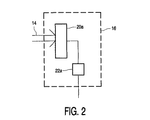
図2はスイッチング制御ユニット16の第1の実施形態を最も簡単な形で表し、ここでは、スイッチングユニット17を制御する唯一の信号が発生される。本実施形態において、スイッチング制御ユニット16は、アドレス/制御バス14に結合されたアドレスコンパレータ20aを含む。コンパレータ20aは状態レジスタ22aに結合された出力を有し、次に状態レジスタはスイッチングユニット17(図示せず)の制御入力に結合された出力を有する。動作中に、コンパレータ20aは、アドレス/制御バス14からのアドレスを設定アドレスと比較する。設定アドレスが検出されたとき、コンパレータ20aは状態レジスタ22aの内容をトグルさせ、状態レジスタは次にスイッチングユニット17に、第1および第2の処理ユニット10a,10bにそれぞれ結合されたメモリユニット18b,18cをスワップさせる。
FIG. 2 represents in a simplest form a first embodiment of the
スイッチング制御ユニット16の別の実施形態は図2に示されたものと同じ構造を有するが、本実施形態では、コンパレータ20aは、(2回の比較を行い、上限アドレスよりも小さいアドレスと下限アドレスよりも大きいアドレスを調べることにより、または、アドレスのより重要な部分だけを使用することにより)アドレスが第1または第2のメモリユニット18b,18c内のロケーションをアドレス指定するアドレス範囲内に含まれるときを通知する。本実施形態において、ユニット22aは範囲内のアドレスがアドレス指定された回数をカウントし、一定の個数のアドレスがカウントされたときに新しい周期の先頭でスイッチングユニット17によって構成されたコネクションを制御する状態レジスタをリセットし、更新するカウンタである。このようなある特定の個数は、あらかじめ定められた個数、または、処理ユニット18b,18cのうちの一方によって実行されるプログラムによって設定されるプログラム可能な個数である。本実施形態では、メモリユニット18b,18cのためのメモリユニットイネーブル信号(各メモリユニット18b,18cがメモリチップで構成される場合にはチップイネーブル)を発生する回路はコンパレータ20aとして使用され、コンパレータは、本例では、選択されたメモリユニットに応じて、メモリユニット18b,18cのいずれかへメモリユニットイネーブル信号を供給するため使用されてもよい。
Another embodiment of the switching
図3はスイッチング制御ユニット16のさらなる実施形態を表す。本実施形態において、スイッチング制御ユニット16は、リードモディファイライトメモリ30、検出器32およびトグルフリップフロップ34を含む。アドレス/制御バス14はリードモディファイライトメモリのアドレス入力に結合され、リードモディファイライトメモリ30のデータ出力は検出器32の入力に結合される。検出器32の出力はトグルフリップフロップ34の入力に結合され、次にトグルフリップフロップはスイッチング制御ユニット16の出力に結合された出力を有する。この検出器32の出力はさらにリードモディファイライトメモリ30のリセット入力に結合される。リードモディファイライトメモリ30は第1および第2のメモリ18b,18cにおいてアドレス指定するため使用され得るアドレス値毎にそれぞれのロケーションを有する。
FIG. 3 represents a further embodiment of the switching
動作中に、本実施形態のスイッチング制御ユニット16は、第1または第2のメモリユニット18a,18bにおけるいずれかのアドレスの繰り返しアドレス指定をチェックすることによりアドレッシングの新しい周期の先頭を検出する。リードモディファイライトメモリ30は、アドレス値毎に、そのアドレス値が現在の周期で使用されたかどうかを示す情報を保持する。第1または第2のメモリ18b,18c内のロケーションをアドレス指定するアドレスは、同様にリードモディファイライトメモリ30内のロケーションをアドレス指定する。最初に、周期の先頭で検出器32はリードモディファイライトメモリ30の内容をリセットする。このようなアドレスが受信されるときにはいつも、リードモディファイライトメモリ30内の対応したロケーションの内容がセットされる。リードモディファイライトメモリ30内のロケーションに先に記憶されていたデータは検出器によってテストされる。このデータがセットされた場合に、検出器32は周期の繰り返しを通知し、トグルフリップフロップ34内のデータ内容をトグルさせ、リードモディファイライトメモリ30の内容をリセットさせる。トグルフリップフロップ34のデータ内容はスイッチングユニット17によって作られたコネクションを制御する。本実施形態は、たとえば、ある種のアドレスがある一定の周期中に使用されないときを無視する、より洗練された周期検出の形式を提供することが可能である。
During operation, the switching
さらなる実施形態において、検出器32は、リードモディファイライトメモリ30から読み出されたデータが周期中に最初にアドレスが使用されたことを示した回数をカウントするカウンタによって置き換えられる。本実施形態において、このカウンタは、あるカウントを超えるとき、新しい周期を通知する(スイッチングユニット17によるスイッチング、リードモディファイライトメモリ30のリセット、および、カウンティングプロセスの新しい周期を引き起こす)。このようにして、スイッチング制御ユニットは、十分な量の異なるロケーション(ある特定の個数よりも多数)がアドレス指定されたときに新しい周期を通知する。ある特定の個数は、あらかじめ定められてもよく、または、たとえば、少なくとも1台の処理ユニットに結合され、カウンタの初期値をセットするレジスタを用いて、処理ユニット10a,10bによりプログラム可能な形でもよい。本実施形態は、たとえば、同じアドレスを用い繰り返されるアクセスオペレーションを無視する、より洗練された周期検出の実現を可能にさせる。
In a further embodiment,
ここまでに図2および3を参照して説明した実施形態は、1本のアドレス/制御バス14のアドレスからの周期検出を表しているが、任意のアドレス/制御バス14,15を使用可能であり、或いは、たとえば、処理ユニット10a,10bのいずれか一つ若しくはそれぞれにおいて新しい周期の先頭が検出されたときに切り替えることにより、これらのバスの組み合わせからのアドレスが使用可能であることが理解されるべきである。スイッチングユニット17が(たとえば、時間インターリーブ方式で、または、調停要求に基づいて)2台以上の処理ユニット10a,10bを同じメモリユニットへ同時に接続することを許容するとき、スイッチング制御ユニット16は、2台のメモリユニット18b,18cの間で互いに独立に処理ユニット10a,10bのバスコネクションを切り替えてもよい。この目的のため、スイッチング制御ユニット16は、2台の検出回路を具備してもよく、各検出回路は、図2または3との関連で説明したタイプのうちの一つであり、それぞれのデータおよびアドレスバスに結合され、アドレスデータバスがメモリユニット18b,18cのどちらに接続されるかを制御する。
The embodiments described so far with reference to FIGS. 2 and 3 represent period detection from the address of one address /
図3aは、バスの組み合わせからのアドレスが使用されるスイッチング制御ユニット16の一実施形態を表す。本実施形態は、第1および第2の繰り返し検出ユニット300a,300bと、状態コンパレータ302と、制御レジスタ304とを含む。繰り返し検出ユニット300a,300bのそれぞれは、図2および3に示されるように、アドレスコンパレータ、または、検出器を備えたリードモディファイライトメモリを含んでもよい。繰り返し検出ユニット300a,300bの出力は状態コンパレータ302に結合され、次に状態コンパレータは制御レジスタ304に結合された更新出力を有する。制御レジスタ304はスイッチングユニット17(図示せず)に結合された制御出力を有する。
FIG. 3a represents an embodiment of the switching
動作中に、繰り返し検出ユニット300a,300bは、たとえば、図2および3に関連して説明したように、対応した処理ユニットからのアドレッシングのパターンの繰り返しを検出する。繰り返しを検出すると、繰り返し検出ユニット300a,300bは状態コンパレータ302へ信号を送信する。簡単な実施形態では、状態コンパレータ302は、対応した繰り返しがセットされるときにセットされた状態ビットを維持し、状態コンパレータは、両方の状態ビットがセットされているならば制御レジスタ304をトグルさせ、状態ビットをクリアする。本実施形態では、特定の処理ユニットからのアクセスオペレーションは、その処理ユニットに対する状態ビットがセットされているならば、好ましくは、一時的に中断される。
During operation, the
別の実施形態では、状態コンパレータ302は、すべての処理ユニットに対する状態ビットがセットされるまで制御レジスタ304の更新を遅延させないが、たとえば、繰り返しが特定の処理ユニットからのアドレスパターンに発生したとき、対象としている処理ユニットの最後のマッピングの交替後に別の処理ユニットからのアドレスのマッピングの交替が起こらない限り、特定の処理ユニットのそれぞれからのアドレスのマッピングを交替させるため更新を発生させる。
In another embodiment, the
スイッチングを制御するためのアドレスの使用だけが簡単な設計を実現するために説明されているが、より複雑な設計では、アドレス/制御バス14,15からのその他の制御信号が同様に使用されることが認められるべきである。たとえば、スイッチング制御ユニット16は、読み出しのため使用されるときに限り、または、書き込みのため使用されるときに限り、アドレスを使用するように設計される。これは、たとえば、読み出しオペレーションを無視する、より洗練された周期検出の実現を可能にさせる。
Although only the use of addresses to control switching has been described to achieve a simple design, other control signals from the address /
さらに、図2および3に示された簡単なスイッチング制御ユニットは、固定アドレス範囲または固定アドレス、における繰り返しを検出することが前提とされているが、代わりに、たとえば、コンパレータ20a内で検出範囲を定める1台以上のプログラム可能なレジスタを使用することにより、プログラム可能な範囲またはプログラム可能なアドレスが使用され制御され、レジスタが少なくとも1台の処理ユニットに結合されるので、この処理ユニットはプログラム制御下でこれらのレジスタに値を書き込むことが可能である。同様に、アドレス範囲検出器が図3の検出器に付加され、アドレス毎にそのアドレスがプログラムされた範囲内に入るかどうかを検出する。アドレスの繰り返しがリードモディファイライトメモリを用いて検出されるとき、繰り返しは、アドレスがプログラムされた範囲内に入る場合に限り通知される。このように、アドレスパターンの繰り返しの検出のための規準はプログラム制御下で使用されるプログラムに応じて調整することができる。同様に、処理ユニット10a,10bの組み合わせからの繰り返し検出のための規準はプログラム制御方式でもよい。
Furthermore, the simple switching control unit shown in FIGS. 2 and 3 is assumed to detect repetition in a fixed address range or a fixed address, but instead, for example, a detection range in the comparator 20a. By using one or more programmable registers to define, a programmable range or programmable address is used and controlled, and this processing unit is program controlled because the registers are coupled to at least one processing unit. It is possible to write values to these registers below. Similarly, an address range detector is added to the detector of FIG. 3 to detect for each address whether the address falls within the programmed range. When an address repeat is detected using the read-modify-write memory, the repeat is notified only if the address falls within the programmed range. In this way, the criteria for detecting address pattern repetition can be adjusted according to the program used under program control. Similarly, the criterion for repeated detection from the combination of the
好ましくは、図2および3を参照して説明された実施形態における繰り返しの検出のため使用されたすべてのアドレスは、メモリユニット18b,18c内のメモリロケーションをアドレス指定するアドレス範囲内のアドレスに限られる。しかし、さらなる実施形態では、その範囲の外側のアドレスが使用されてもよい。かくして、スイッチングユニット17を介して接続されたメモリユニット18b,18c内のアドレスを含むアクセスパターンの大きい変化を許容することが可能であると共に、これらのメモリユニット18b,18c内のアドレスの範囲の外側のアドレスを使用して、繰り返しの検出が依然として可能である。
Preferably, all addresses used for repeat detection in the embodiment described with reference to FIGS. 2 and 3 are limited to addresses within the address range addressing memory locations in
図4はスイッチングユニット17の一実施形態を表す。本実施形態は、選択可能なアドレス/データバスドライバ40a,40b,42a,42bを含む。第1のアドレス/データバスドライバ40aは、一方で第1の処理ユニット10a(図示せず)のアドレス/制御バス14とデータバス12との間に接続され、他方で第1のメモリユニット18a(図示せず)のためのデータ/アドレスコネクションに接続される。第2のアドレス/データバスドライバ40bは、一方で第1の処理ユニット10a(図示せず)のアドレス/制御バス14とデータバス12との間に接続され、他方で第2のメモリユニット18b(図示せず)のためのデータ/アドレスコネクションに接続される。第3のアドレス/データバスドライバ42aは、一方で第2の処理ユニット10b(図示せず)のアドレス/制御バス15とデータバス13との間に接続され、他方で第1のメモリユニット18a(図示せず)のためのデータ/アドレスコネクションに接続される。第4のアドレス/データバスドライバ42bは、一方で第2の処理ユニット10b(図示せず)のアドレス/制御バス15とデータバス13との間に接続され、他方で第2のメモリユニット18b(図示せず)のためのデータ/アドレスコネクションに接続される。
FIG. 4 shows an embodiment of the switching
スイッチングユニット17は、アドレス/データバスドライバ40a,40b,42a,42bの入力を有効にするため結合された制御信号のための入力44を有するので、スイッチ制御ユニット16(図示せず)からの制御信号に応じて、第1および第4のアドレス/データバスドライバ40a,42bが同時にイネーブルにされるか、または、第2および第3のアドレス/データバスドライバ40b,42aが同時にイネーブルにされる。イネーブルにされると、アドレス/データバスドライバ40a,40b,42a,42bはデータ信号およびアドレス信号を送る。
Since the switching
メモリユニット18a,18bへの共有アクセスを可能にさせるある種の共有機構(たとえば、タイムスロット多重化機構、優先度機構、または、アービトレーション機構)が設けられるならば、本発明の範囲から逸脱することなく、より複雑な制御信号、たとえば、第1および第2のアドレス/データバスドライバ40a,40bを第3および第4のアドレス/データバスドライバ42a,42bとは独立に制御することができる信号が使用されてもよい。
Depart from the scope of the present invention if some kind of sharing mechanism (eg, time slot multiplexing mechanism, priority mechanism, or arbitration mechanism) is provided that allows shared access to the
スイッチングユニット17は、非常に多数の処理ユニットまたはメモリユニットをサポートするように拡張することが容易である。より多くの処理ユニットがより多くのアドレス/データバスドライバを追加することによりサポートされ、より多くのメモリユニットがより多くのアドレス/データバスドライバを一体的に接続することによりサポートされる。3台以上のメモリユニットが、たとえば、処理ユニット10a,10bからのアドレスをラウンドロビン方式で様々なメモリへマッピングするため使用されてもよい。この目的のため、図2および3に示されたトグルフリップフロップの代わりに、巡回カウンタが処理ユニット10a,10bのそれぞれに使用されてもよく、メモリユニット18a,18bのうちのどちらが処理ユニット10a,10bのそれぞれによってアドレス指定されるかを選択する。これは、繰り返しが検出されると、メモリ競合を生じさせることなく、個別の処理ユニット10a,10bからのアドレスのマッピングの切り替えを容易に可能にさせる。プログラム制御下で、メモリユニット18a,18bの異なるサイクルが選択されてもよく、たとえば、第1のメモリユニットのペアの間で一部のアドレスのアドレス指定を交互に行い、第2のメモリユニットのペアの間で他のアドレスのアドレス指定を交互に行い、または、3台のメモリユニットの中でアドレスのマッピングを循環させる。
The switching
この装置は、処理ユニット10a,10bがそれぞれのメモリユニット18a,18bにおけるロケーションを同じアドレスを用いてアドレス指定できるようにすることが理解されるであろう。ロケーションがアドレス指定されるメモリユニットの制御は、処理ユニットの外部にあり、周期的パターンの繰り返しの先頭の検出に応じて切り替えるよう選択するスイッチング制御ユニットによって行われる。いずれかの処理ユニット10a,10bからの同じアドレスは、スイッチング制御ユニット16の状態に応じて、異なるメモリユニット18a,18b内のロケーションをアドレス指定するが、メモリユニット18a,18b内のロケーションが、異なる処理ユニット10a,10bからの同じアドレスによってアドレス指定されることは厳密には必要でない。(メモリユニット18a,18b内でアドレスを区別するために必要ではないアドレスのより上位部分(significant part)の削除(suppression)だけであるとしても)ある種のアドレス変換機構が処理ユニット10a,10bとメモリユニット18a,18bとの間に組み込まれてもよく、異なるアドレスが、そのアドレスを供給する方の処理ユニットに応じて、同じロケーションをアドレス指定する。
It will be appreciated that this apparatus allows the
Claims (11)
それぞれがアドレス入力およびデータ入出力を有する複数台のメモリユニットと、
スイッチングユニットと、
を具備し、
前記スイッチングユニットが、
前記処理ユニットの前記データ入出力と、前記メモリユニットの前記データ入出力より選択可能なデータ入出力との間にある第1の選択可能なコネクションと、
前記処理ユニットの前記アドレス出力から、前記メモリユニットより選択可能なメモリユニットの前記アドレス入力への第2の選択可能なコネクションと、
前記処理ユニットの前記アドレス出力に結合され、少なくとも1台の前記処理ユニットによって出力されたアドレスパターンの周期の繰り返しを検出するため配置された検出ユニットと、
新しい1回の繰り返しの検出に応答して前記第1および第2の選択可能なコネクションを切り替えるため、前記検出ユニットに結合された入力を有し、前記第1および第2の選択可能なコネクションを制御する状態保持エレメントと、
を具備し、これにより、前記データ処理ユニットからの同一のアドレスが連続的な繰り返しの間に前記メモリユニットのうちの異なるメモリユニットへ交互にマッピングされる、
データ処理装置。 A plurality of data processing units each having an address output and data input / output;
A plurality of memory units each having an address input and data input / output;
A switching unit;
Comprising
The switching unit is
A first selectable connection between the data input / output of the processing unit and a data input / output selectable from the data input / output of the memory unit;
A second selectable connection from the address output of the processing unit to the address input of a memory unit selectable from the memory unit;
A detection unit coupled to the address output of the processing unit and arranged to detect repetition of a period of an address pattern output by at least one of the processing units;
In order to switch the first and second selectable connections in response to a new one-time detection, the first and second selectable connections have inputs coupled to the detection unit. A state retaining element to control;
Whereby the same address from the data processing unit is alternately mapped to different ones of the memory units during successive iterations.
Data processing device.
少なくとも前記ある特定の回数まで前記範囲内で前記第1のデータ処理ユニットの前記アドレス出力からのアドレスのカウント回数をカウントするカウンタを具備する、請求項3に記載のデータ処理装置。 The certain number of times is two or more,
4. The data processing device according to claim 3, further comprising a counter that counts the number of address counts from the address output of the first data processing unit within the range up to at least the certain number of times.
前記アクセスメモリが前記第1のデータ処理ユニットによってアドレス指定可能である前記メモリユニット内のロケーションをアドレス指定する複数個のアドレスに対するロケーションを具備し、
前記アクセスメモリが前記メモリユニット内の前記ロケーションへのアクセスを記録し、
前記検出ユニットは、前記アクセスメモリが前記第1の処理ユニットによって供給されたアドレスが繰り返し中に先に供給されたことを示すかどうかに応じて、前記新しい繰り返しを示す検出信号を生成する、
請求項1に記載のデータ処理装置。 The detection unit comprises an access memory for the at least one data processing unit;
The access memory comprises locations for a plurality of addresses addressing locations within the memory unit that are addressable by the first data processing unit;
The access memory records access to the location in the memory unit;
The detection unit generates a detection signal indicating the new iteration depending on whether the access memory indicates that the address supplied by the first processing unit was previously supplied during the iteration;
The data processing apparatus according to claim 1.
前記処理ユニットのデータ入出力と複数台のメモリユニットのうちの選択可能なメモリユニットのデータ入出力との間で選択可能なコネクションを切り替え、これにより、少なくとも1台の前記処理ユニットからの同じアドレスが前記繰り返しの検出に応じて前記メモリユニットのうちの異なるメモリユニット内のロケーションを交互にアドレス指定する、
データ処理方法。 Detecting the repetition of the cycle of the access address pattern output from at least one of the plurality of processing units;
A selectable connection is switched between data input / output of the processing unit and data input / output of a selectable memory unit among a plurality of memory units, whereby the same address from at least one processing unit Alternately address locations within different memory units of the memory units in response to detection of the repetition;
Data processing method.
Applications Claiming Priority (2)
| Application Number | Priority Date | Filing Date | Title |
|---|---|---|---|
| EP02079612 | 2002-11-05 | ||
| PCT/IB2003/004427 WO2004042591A1 (en) | 2002-11-05 | 2003-10-08 | Data processing apparatus with address redirection in response to periodic address patterns |
Publications (1)
| Publication Number | Publication Date |
|---|---|
| JP2006505845A true JP2006505845A (en) | 2006-02-16 |
Family
ID=32309402
Family Applications (1)
| Application Number | Title | Priority Date | Filing Date |
|---|---|---|---|
| JP2004549403A Withdrawn JP2006505845A (en) | 2002-11-05 | 2003-10-08 | Data processing apparatus for redirecting addresses in response to periodic address patterns |
Country Status (9)
| Country | Link |
|---|---|
| US (1) | US20060041692A1 (en) |
| EP (1) | EP1563401B1 (en) |
| JP (1) | JP2006505845A (en) |
| CN (1) | CN1711528A (en) |
| AT (1) | ATE346342T1 (en) |
| AU (1) | AU2003264788A1 (en) |
| DE (1) | DE60309923T2 (en) |
| TW (1) | TW200416553A (en) |
| WO (1) | WO2004042591A1 (en) |
Families Citing this family (1)
| Publication number | Priority date | Publication date | Assignee | Title |
|---|---|---|---|---|
| CN100583072C (en) * | 2006-10-13 | 2010-01-20 | 鸿富锦精密工业(深圳)有限公司 | Controller, address control method and bus data-transmission system using the same |
Family Cites Families (15)
| Publication number | Priority date | Publication date | Assignee | Title |
|---|---|---|---|---|
| JPS5835627A (en) * | 1981-08-26 | 1983-03-02 | Toshiba Corp | Controlling system for memory data prefetch |
| JPS62206658A (en) * | 1986-03-07 | 1987-09-11 | Hitachi Ltd | Memory controller |
| US4933846A (en) * | 1987-04-24 | 1990-06-12 | Network Systems Corporation | Network communications adapter with dual interleaved memory banks servicing multiple processors |
| US4920484A (en) * | 1988-10-05 | 1990-04-24 | Yale University | Multiprocessor/memory interconnection network wherein messages sent through the network to the same memory are combined |
| JP3203701B2 (en) * | 1990-11-01 | 2001-08-27 | インターナショナル・ビジネス・マシーンズ・コーポレーション | Code segment linking method and system, and code segment dynamic linking method |
| US5551054A (en) * | 1991-11-19 | 1996-08-27 | Adaptec, Inc. | Page mode buffer controller for transferring Nb byte pages between a host and buffer memory without interruption except for refresh |
| JP3178909B2 (en) * | 1992-01-10 | 2001-06-25 | 株式会社東芝 | Semiconductor memory device |
| JPH0619785A (en) * | 1992-03-27 | 1994-01-28 | Matsushita Electric Ind Co Ltd | Distributed shared virtual memory and its constitution method |
| US5519839A (en) * | 1992-10-02 | 1996-05-21 | Compaq Computer Corp. | Double buffering operations between the memory bus and the expansion bus of a computer system |
| US5777628A (en) * | 1996-05-29 | 1998-07-07 | Hewlett-Packard Company | Method and apparatus for detecting cache collisions in a two dimensional memory |
| US5884050A (en) * | 1996-06-21 | 1999-03-16 | Digital Equipment Corporation | Mechanism for high bandwidth DMA transfers in a PCI environment |
| US6170046B1 (en) * | 1997-10-28 | 2001-01-02 | Mmc Networks, Inc. | Accessing a memory system via a data or address bus that provides access to more than one part |
| US7433948B2 (en) * | 2002-01-23 | 2008-10-07 | Cisco Technology, Inc. | Methods and apparatus for implementing virtualization of storage within a storage area network |
| US6816989B2 (en) * | 2001-12-28 | 2004-11-09 | Hewlett-Packard Development Company, L.P. | Method and apparatus for efficiently managing bandwidth of a debug data output port or buffer |
| US7617329B2 (en) * | 2002-12-30 | 2009-11-10 | Intel Corporation | Programmable protocol to support coherent and non-coherent transactions in a multinode system |
-
2003
- 2003-10-08 DE DE60309923T patent/DE60309923T2/en not_active Expired - Fee Related
- 2003-10-08 US US10/533,506 patent/US20060041692A1/en not_active Abandoned
- 2003-10-08 EP EP03810543A patent/EP1563401B1/en not_active Expired - Lifetime
- 2003-10-08 WO PCT/IB2003/004427 patent/WO2004042591A1/en active IP Right Grant
- 2003-10-08 JP JP2004549403A patent/JP2006505845A/en not_active Withdrawn
- 2003-10-08 AU AU2003264788A patent/AU2003264788A1/en not_active Abandoned
- 2003-10-08 CN CNA2003801027707A patent/CN1711528A/en active Pending
- 2003-10-08 AT AT03810543T patent/ATE346342T1/en not_active IP Right Cessation
- 2003-10-31 TW TW092130496A patent/TW200416553A/en unknown
Also Published As
| Publication number | Publication date |
|---|---|
| DE60309923D1 (en) | 2007-01-04 |
| EP1563401A1 (en) | 2005-08-17 |
| AU2003264788A1 (en) | 2004-06-07 |
| ATE346342T1 (en) | 2006-12-15 |
| DE60309923T2 (en) | 2007-10-18 |
| WO2004042591A1 (en) | 2004-05-21 |
| US20060041692A1 (en) | 2006-02-23 |
| TW200416553A (en) | 2004-09-01 |
| CN1711528A (en) | 2005-12-21 |
| EP1563401B1 (en) | 2006-11-22 |
Similar Documents
| Publication | Publication Date | Title |
|---|---|---|
| JP4856379B2 (en) | Protocol conversion arbitration circuit, system including the same, and signal conversion arbitration method | |
| JP2007215203A (en) | Data processing method and data processing unit, dynamic reconfiguration method of configurable element, system and process | |
| CN106021141B (en) | Semiconductor device with a plurality of semiconductor chips | |
| JP2018518773A (en) | Event generator | |
| TW201643684A (en) | System and method for configuring a plurality of registers with soft error detection and low wiring complexity | |
| JP2009238001A (en) | Computer system | |
| JP2008502974A (en) | Interface device for debugging and / or tracing a computer system having one or more masters and one or more slaves working together | |
| JP2005524851A (en) | Tester system having a plurality of instruction memories | |
| JP4642531B2 (en) | Arbitration of data requests | |
| JP2006505845A (en) | Data processing apparatus for redirecting addresses in response to periodic address patterns | |
| JP4193746B2 (en) | Matrix bus connection system | |
| JP4359618B2 (en) | Configuration register access method, setting method, integrated circuit parts, computer system, product | |
| JP2007087247A (en) | Bus control system | |
| CN112685349B (en) | Bit operation control system and method with variable bit width | |
| JP2007148622A (en) | Interface setting method | |
| JP2007506174A (en) | Integrated circuit having a plurality of communication digital signal processors | |
| JP2005010966A (en) | Lsi device | |
| JP2008102759A (en) | Memory access controller | |
| JP3959407B2 (en) | Image processing apparatus and image processing system | |
| KR20090012128A (en) | Transfer device, information processing apparatus having transfer device, and controlling method | |
| JP6535516B2 (en) | Multi-programmable device system and control method thereof | |
| JP2001167049A (en) | Bus arbitrating device | |
| JP2010033452A (en) | Register control circuit and register control method | |
| JP3754765B2 (en) | Data processing device | |
| JP2000132527A (en) | Inter-processor communication controller |
Legal Events
| Date | Code | Title | Description |
|---|---|---|---|
| A621 | Written request for application examination |
Free format text: JAPANESE INTERMEDIATE CODE: A621 Effective date: 20061006 |
|
| RD02 | Notification of acceptance of power of attorney |
Free format text: JAPANESE INTERMEDIATE CODE: A7422 Effective date: 20070426 |
|
| A761 | Written withdrawal of application |
Free format text: JAPANESE INTERMEDIATE CODE: A761 Effective date: 20070718 |