JP4642531B2 - Arbitration of data requests - Google Patents
Arbitration of data requests Download PDFInfo
- Publication number
- JP4642531B2 JP4642531B2 JP2005106228A JP2005106228A JP4642531B2 JP 4642531 B2 JP4642531 B2 JP 4642531B2 JP 2005106228 A JP2005106228 A JP 2005106228A JP 2005106228 A JP2005106228 A JP 2005106228A JP 4642531 B2 JP4642531 B2 JP 4642531B2
- Authority
- JP
- Japan
- Prior art keywords
- data
- memory
- access
- operable
- buses
- Prior art date
- Legal status (The legal status is an assumption and is not a legal conclusion. Google has not performed a legal analysis and makes no representation as to the accuracy of the status listed.)
- Active
Links
- 230000015654 memory Effects 0.000 claims description 172
- 238000012545 processing Methods 0.000 claims description 69
- 238000012546 transfer Methods 0.000 claims description 27
- 238000000034 method Methods 0.000 claims description 12
- 230000004044 response Effects 0.000 claims description 7
- 238000004891 communication Methods 0.000 claims description 3
- 238000010586 diagram Methods 0.000 description 5
- LHMQDVIHBXWNII-UHFFFAOYSA-N 3-amino-4-methoxy-n-phenylbenzamide Chemical compound C1=C(N)C(OC)=CC=C1C(=O)NC1=CC=CC=C1 LHMQDVIHBXWNII-UHFFFAOYSA-N 0.000 description 4
- 230000004913 activation Effects 0.000 description 4
- 230000001154 acute effect Effects 0.000 description 1
- 230000006399 behavior Effects 0.000 description 1
- 230000001419 dependent effect Effects 0.000 description 1
- 238000013507 mapping Methods 0.000 description 1
- 238000012986 modification Methods 0.000 description 1
- 230000004048 modification Effects 0.000 description 1
- 238000012544 monitoring process Methods 0.000 description 1
- 230000008569 process Effects 0.000 description 1
Images


Classifications
-
- G—PHYSICS
- G06—COMPUTING; CALCULATING OR COUNTING
- G06F—ELECTRIC DIGITAL DATA PROCESSING
- G06F13/00—Interconnection of, or transfer of information or other signals between, memories, input/output devices or central processing units
- G06F13/14—Handling requests for interconnection or transfer
- G06F13/16—Handling requests for interconnection or transfer for access to memory bus
- G06F13/1605—Handling requests for interconnection or transfer for access to memory bus based on arbitration
- G06F13/1652—Handling requests for interconnection or transfer for access to memory bus based on arbitration in a multiprocessor architecture
- G06F13/1657—Access to multiple memories
-
- G—PHYSICS
- G06—COMPUTING; CALCULATING OR COUNTING
- G06F—ELECTRIC DIGITAL DATA PROCESSING
- G06F13/00—Interconnection of, or transfer of information or other signals between, memories, input/output devices or central processing units
- G06F13/14—Handling requests for interconnection or transfer
- G06F13/16—Handling requests for interconnection or transfer for access to memory bus
- G06F13/1605—Handling requests for interconnection or transfer for access to memory bus based on arbitration
-
- G—PHYSICS
- G06—COMPUTING; CALCULATING OR COUNTING
- G06F—ELECTRIC DIGITAL DATA PROCESSING
- G06F13/00—Interconnection of, or transfer of information or other signals between, memories, input/output devices or central processing units
- G06F13/14—Handling requests for interconnection or transfer
- G06F13/20—Handling requests for interconnection or transfer for access to input/output bus
- G06F13/28—Handling requests for interconnection or transfer for access to input/output bus using burst mode transfer, e.g. direct memory access DMA, cycle steal
Landscapes
- Engineering & Computer Science (AREA)
- Theoretical Computer Science (AREA)
- Physics & Mathematics (AREA)
- General Engineering & Computer Science (AREA)
- General Physics & Mathematics (AREA)
- Bus Control (AREA)
- Memory System (AREA)
Description
本発明はデータ処理システムの分野に関する。より詳細には、本発明はデータ転送要求の分野に関する。 The present invention relates to the field of data processing systems. More particularly, the present invention relates to the field of data transfer requests.
データ処理システムでは、あるメモリから別のメモリに、又は外部データ・ソースとデータ・プロセッサに関連付けられているメモリとの間でデータを転送することがしばしば必要である。例えば、コードを、起動時にフラッシュなどの低速メモリに格納し、使用前にプロセッサに関連付けられているより速い命令メモリ(instruction memory)に転送することが望ましい場合がある。一般にこうした転送は、データが読み取られるフラッシュ・メモリ内の位置、及びデータ項目が書き込まれるコア内のレジスタを指定するロード命令、並びにコア内のレジスタ、及びより速い命令メモリ内の宛先位置を指定するストア命令により、データ・プロセッサ・コアを介して行われる。こうした転送は、かなり遅く、各データ項目にいくつかの命令がかかるので、命令の点で高くつく。 In data processing systems, it is often necessary to transfer data from one memory to another or between an external data source and a memory associated with the data processor. For example, it may be desirable to store code in a slow memory, such as flash, at startup and transfer it to a faster instruction memory associated with the processor prior to use. In general, such transfers specify the location in flash memory from which data is read and the load instruction that specifies the register in the core to which the data item is written, as well as the register in the core and the destination location in the faster instruction memory. This is done via the data processor core by a store instruction. Such transfers are fairly slow and costly in terms of instructions because each data item takes several instructions.
データ転送が相対的に遅く命令の点で高くつく問題は、データ・ロギングなど、常にプロセッサを介して大量のデータをメモリに転送することが必要となり得るアプリケーションにおいて特に重大となる場合がある。 The problem of data transfer being relatively slow and expensive in terms of instructions can be particularly serious in applications where it may be necessary to always transfer large amounts of data to memory via a processor, such as data logging.
一態様から見ると、本発明は、外部データ・ソースとデータ・プロセッサ・コアに関連付けられている少なくとも1つのメモリとの間でデータ転送操作を実行するように動作可能なメモリ・アクセス・インターフェイス部分と、データ処理操作を実行するように動作可能なデータ処理部分と、前記プロセッサ・コアから少なくとも2つのバスにデータを転送するように動作可能な読み取り/書き込みポートであって、前記少なくとも2つのバスが前記プロセッサ・コアと前記少なくとも1つのメモリとの間にデータ通信を提供するように動作可能であり、前記少なくとも1つのメモリが少なくとも2つの部分を含み、前記少なくとも2つのバスのそれぞれが前記少なくとも2つの部分のそれぞれにデータ・アクセスを提供するように動作可能である読み取り/書き込みポートと、前記読み取り/書き込みポートに関連付けられているアービトレーション・ロジックとを含み、前記アービトレーション・ロジックが、前記メモリ・アクセス・インターフェイスから受信された前記少なくとも1つのメモリの一部にあるデータのアクセスを要求するデータ・アクセス要求を、前記少なくとも1つのメモリの前記一部にアクセスを提供する前記少なくとも2つのバスのうちの一方に経路設定し、前記データ処理部分から受信された前記少なくとも1つのメモリの別の一部にあるデータのアクセスを要求する別のデータ・アクセス要求を、前記少なくとも1つのメモリの前記別の一部にアクセスを提供する前記少なくとも2つのバスのうちのもう一方に経路設定するように動作可能であり、前記データ・アクセス要求の前記経路設定が同じクロック・サイクル中に実行される、データ・プロセッサ・コアを提供する。 Viewed from one aspect, the present invention provides a memory access interface portion operable to perform data transfer operations between an external data source and at least one memory associated with a data processor core. A data processing portion operable to perform data processing operations and a read / write port operable to transfer data from the processor core to at least two buses, the at least two buses Is operable to provide data communication between the processor core and the at least one memory, the at least one memory including at least two portions, each of the at least two buses being the at least Operates to provide data access to each of the two parts A read / write port and arbitration logic associated with the read / write port, wherein the arbitration logic is in a portion of the at least one memory received from the memory access interface A data access request requesting access to data is routed to one of the at least two buses providing access to the portion of the at least one memory and the at least received from the data processing portion The other of the at least two buses providing access to another portion of the at least one memory for requesting access to data in another portion of the one memory Is operable to route to Serial The routing of data access requests are performed during the same clock cycle, to provide a data processor core.
本発明は、一部の状況で、データを特定のメモリに、又は特定のメモリから迅速に転送することができることが特に重要であることを認識している。本発明は、メモリ・アクセス・インターフェイスを提供することによってこの問題に対処する。コアをいくつかの部分に分割することにはいくつかの利点があり、1つは、データを読み取り、それをコアのレジスタに格納し、次いでメモリに書き込むのに必要な命令が不要であるため、データが標準プロセッサ・コアを介して転送された場合より速く転送され得ることである。しかし、コアのメモリ・アクセス・インターフェイス部分を処理部分とともに提供することに関連する問題は、両方の部分が関連のメモリに格納されているデータに同時にアクセスしようとする可能性があることである。この問題は、データ・ロギングなど、すぐに処理する必要のない大量のデータがコアを介してメモリに転送されるアプリケーションにおいて特に重大となる場合がある。 The present invention recognizes that in some situations it is particularly important that data can be transferred quickly to or from a particular memory. The present invention addresses this problem by providing a memory access interface. There are several advantages to splitting the core into parts, because one does not need the instructions needed to read the data, store it in the core's registers, and then write it to memory , Data can be transferred faster than when transferred through a standard processor core. However, a problem associated with providing the memory access interface portion of the core along with the processing portion is that both portions may attempt to simultaneously access data stored in the associated memory. This problem can be particularly acute in applications where large amounts of data that do not need to be processed immediately, such as data logging, are transferred to memory through the core.
この問題は、プロセッサ・コアと関連のメモリとの間にデータ通信を提供するように動作可能な少なくとも2つのバスを提供することによって対処され、関連のメモリは少なくとも2つの部分に分割され、バスがそれぞれの部分にデータ・アクセスを提供する。アービトレーション・ロジックは、バス及び読み取り/書き込みポートと関連して提供され、メモリの特定の部分にあるデータへのアクセスを要求するデータ・アクセス要求を適切なバスに経路設定するように動作可能である。複数のバスの提供によって、同じクロック・サイクルでコアのメモリ・アクセス・インターフェイス及びデータ処理部分から受信されるメモリの異なる部分へのデータ・アクセス要求をそれぞれのバスに沿って並行して処理できるようになる。これによって、コアの2つの部分が単一のバスを介して1つのメモリにアクセスしようと試みているときに起こり得る問題の一部が軽減される。 This problem is addressed by providing at least two buses operable to provide data communication between the processor core and the associated memory, the associated memory being divided into at least two parts, the bus Provides data access to each part. Arbitration logic is provided in association with the bus and read / write ports and is operable to route data access requests that require access to data in a particular portion of memory to the appropriate bus. . The provision of multiple buses allows data access requests to different parts of the memory received from the core memory access interface and data processing part in the same clock cycle to be processed in parallel along each bus. become. This alleviates some of the problems that can occur when two parts of the core are attempting to access a single memory over a single bus.
好ましい実施例では、アービトレーション・ロジックは、前記データ・アクセス要求に関連付けられている前記少なくとも1つのメモリ内のアドレス位置に基づいて前記データ・アクセス要求を経路設定する前記少なくとも2つのバスのうちの一方を選択するように動作可能である。 In a preferred embodiment, the arbitration logic is one of the at least two buses that routes the data access request based on an address location in the at least one memory associated with the data access request. Is operable to select.
データに関連付けられているアドレスは、データが格納されているメモリの部分の指示を提供し、したがってどのバスを使用するかを決定するためにアービトレーション・ロジックによって使用することができる有用なインジケータである。 The address associated with the data provides an indication of the portion of memory where the data is stored and is therefore a useful indicator that can be used by the arbitration logic to determine which bus to use .
好ましい実施例では、前記メモリの前記少なくとも2つの部分は、命令を格納するように動作可能である命令部分、及びデータ項目を格納するように動作可能である少なくとも1つのデータ部分を含み、前記アービトレーション・ロジックは、転送すべきデータが命令であるとき、前記命令部分へのアクセスを提供する前記少なくとも2つのバスのうちの第1のものに前記アクセス要求を経路設定し、転送すべきデータがデータ項目であるとき、前記少なくとも1つのデータ部分へのアクセスを提供する前記少なくとも2つのバスのうちの第2のものに前記データ・アクセス要求を経路設定するように動作可能である。 In a preferred embodiment, the at least two portions of the memory include an instruction portion operable to store instructions and at least one data portion operable to store data items, the arbitration The logic routes the access request to a first one of the at least two buses providing access to the instruction portion when the data to be transferred is an instruction, and the data to be transferred is data When an item is operable to route the data access request to a second of the at least two buses providing access to the at least one data portion.
メモリを命令部分及びデータ部分に分割することは、メモリを分割する実際の方法である。 Dividing the memory into an instruction part and a data part is an actual way of dividing the memory.
好ましくは、前記少なくとも1つのデータ部分は、偶数アドレスを有するデータを格納するように動作可能な偶数データ部分、及び奇数アドレスを有するデータを格納するように動作可能な奇数データ部分の2つのデータ部分を含み、前記読み取り/書き込みポートは、前記命令部分へのアクセスを提供する第1のバス、前記奇数データ部分へのアクセスを提供する第2のバス、及び前記偶数データ部分へのアクセスを提供する第3のバスの3つのバスを介して前記プロセッサ・コアと前記少なくとも1つのメモリとの間にデータを転送するように動作可能であり、前記アービトレーション・ロジックは、転送すべきデータが命令であるときは前記第1のバスに、転送すべきデータが奇数アドレスに関連付けられているデータ項目であるときは前記第2のバスに、転送すべきデータが偶数アドレスに関連付けられているデータ項目であるときは前記第3のバスにデータ・アクセス要求を経路設定するように動作可能である。 Preferably, the at least one data portion is two data portions, an even data portion operable to store data having even addresses and an odd data portion operable to store data having odd addresses. And the read / write port provides a first bus providing access to the instruction portion, a second bus providing access to the odd data portion, and access to the even data portion. Operable to transfer data between the processor core and the at least one memory via three buses of a third bus, wherein the arbitration logic is that the data to be transferred is an instruction When the data to be transferred to the first bus is a data item associated with an odd address The second bus, when the data to be transferred is a data item that is associated with the even address is operable to route the data access request to said third bus.
データ部分を奇数アドレス部分及び偶数アドレス部分に分割することによって、同時に格納された大量のデータ項目にアクセスするデータ・アクセス要求は、交互のデータ・バスを使用する。これは、プロセッサ・コアの部分のうちの1つがデータ・バスのうちの1つを長時間独占する可能性がほとんどなく、それによってプロセッサ・コアの他方の部分によるメモリの対応する部分へのアクセスが防止されることを意味する。 Data access requests to access a large number of data items stored simultaneously by dividing the data portion into odd and even address portions use alternating data buses. This is unlikely that one of the processor core parts will monopolize one of the data buses for a long time, thereby allowing the other part of the processor core to access the corresponding part of the memory. Is prevented.
好ましい実施例では、前記アービトレーション・ロジックは、前記少なくとも1つのメモリの一部にあるデータへのアクセスを要求する、前記メモリ・アクセス・インターフェイス部分からのデータ・アクセス要求、及び前記データ処理部分からのデータ・アクセス要求の両方のデータ・アクセス要求の前記受信に応答して、前記処理部分からの前記要求を前記少なくとも2つのバスのうちの前記一方に経路設定する前に、前記メモリ・アクセス・インターフェイス部分からの前記データ・アクセス要求を、前記少なくとも1つのメモリの前記一部にデータ・アクセスを提供する前記少なくとも2つのバスのうちの一方に経路設定するように動作可能である。 In a preferred embodiment, the arbitration logic includes a data access request from the memory access interface portion requesting access to data in the at least one memory portion, and from the data processing portion. The memory access interface prior to routing the request from the processing portion to the one of the at least two buses in response to the receipt of both data access requests. The data access request from a portion is operable to route to one of the at least two buses that provides data access to the portion of the at least one memory.
アービトレーション・ロジックは、同じプロセッサ・クロック・サイクル中に両方の部分からのデータ・アクセス要求が受信されたときにメモリ・アクセス・インターフェイスに優先権を与えるように動作可能である。これは、メモリ・アクセス・インターフェイスは、メモリへの高速アクセスを提供するためにプロセッサ・コアに設けられているからであり、したがって、それに優先権を与えることは理解できる。特に重要なコードがコアの処理部分によって実行されている場合、コアの処理部分が長時間にわたってメモリへのアクセスを拒否されることによってコアの動作に重大な影響を及ぼす可能性があり、複数のバスの提供は、それを防ぐのを助ける。 The arbitration logic is operable to give priority to the memory access interface when data access requests from both parts are received during the same processor clock cycle. This is because the memory access interface is provided in the processor core to provide fast access to the memory, and therefore it is understandable to give it priority. If particularly important code is being executed by the core processing part, the core processing part may have a significant impact on the core's behavior by being denied access to memory for an extended period of time. Providing a bus will help prevent it.
有利には、前記アービトレーション・ロジックは、前記少なくとも1つのメモリの少なくとも1つのビジー部分から待機要求を検出するように動作可能であり、前記アービトレーション・ロジックは、前記待機要求が検出されなくなるまで、任意のデータ・アクセス要求を前記ビジー部分に経路設定しないように動作可能である。 Advantageously, the arbitration logic is operable to detect a wait request from at least one busy portion of the at least one memory, and the arbitration logic is optional until the wait request is no longer detected. The data access request is not routed to the busy portion.
一部の実施例では、メモリは、プロセッサ・クロックほど速く動作しない場合がある。こうした場合、アービトレーション・ロジックが理解できる待機信号を使用できることが非常に便利である。これによって、プロセッサが対応できるよりも速くデータ・アクセス要求がメモリに、又はメモリから送信されるのを防ぐ。 In some embodiments, the memory may not run as fast as the processor clock. In such a case, it is very convenient to be able to use a wait signal that the arbitration logic can understand. This prevents data access requests from being sent to or from memory faster than the processor can accommodate.
本発明の第2の態様は、本発明の第1の態様によるデータ処理コア、少なくとも2つの部分に分割される少なくとも1つのメモリ、及び前記少なくとも1つのメモリの前記少なくとも2つの部分のそれぞれの部分へのデータ・アクセスをそれぞれ可能にする少なくとも2つのバスを含むデータ処理装置を提供する。 A second aspect of the invention comprises a data processing core according to the first aspect of the invention, at least one memory divided into at least two parts, and respective parts of the at least two parts of the at least one memory. A data processing apparatus is provided that includes at least two buses each enabling data access to the network.
有利には、前記少なくとも1つのメモリは厳重に制御されたメモリである。 Advantageously, said at least one memory is a tightly controlled memory.
本発明の実施例によって異なる種類のメモリを使用することはできるが、本発明は、特に厳重に制御されたメモリの扱いによく対応している。 Although different types of memory may be used depending on the embodiment of the present invention, the present invention is particularly well suited for handling tightly controlled memories.
本発明の第3の態様は、外部データ・ソースとデータ・プロセッサ・コアに関連付けられている少なくとも1つのメモリとの間にデータを転送する方法を提供し、前記データ・プロセッサ・コアは、前記外部データ・ソースと前記データ・プロセッサ・コアに関連付けられている前記少なくとも1つのメモリとの間のデータ転送操作を実行するように動作可能であるメモリ・アクセス・インターフェイス部分、及びデータ処理操作を実行するように動作可能であるデータ処理部分を含み、前記方法は、前記メモリ・アクセス・インターフェイス部分から受信された前記少なくとも1つのメモリの一部にあるデータのアクセスを要求するデータ・アクセス要求、及び前記データ処理部分から受信された前記少なくとも1つのメモリの別の部分にあるデータへのアクセスを要求するデータ・アクセス要求に応答して、前記メモリ・アクセス・インターフェイス部分から受信された前記データ・アクセス要求を少なくとも2つのバスのうちの一方に経路設定するステップであって、前記少なくとも2つのバスのうちの前記一方が前記少なくとも1つのメモリの前記一部へのアクセスを提供するステップと、前記データ処理部分から受信された前記データ・アクセス要求を前記少なくとも2つのバスのうちのもう一方のバスに経路設定するステップであって、前記もう一方のバスが前記少なくとも1つのメモリの前記別の部分へのアクセスを提供するステップとを含み、前記データ・アクセス要求の前記経路設定は、同じクロック・サイクル中に実行される。 A third aspect of the present invention provides a method for transferring data between an external data source and at least one memory associated with a data processor core, the data processor core comprising: A memory access interface portion operable to perform data transfer operations between an external data source and the at least one memory associated with the data processor core, and perform data processing operations A data access request operable to: a data access request for requesting access to data in a portion of the at least one memory received from the memory access interface portion; and Another portion of the at least one memory received from the data processing portion; Routing the data access request received from the memory access interface portion to one of at least two buses in response to a data access request requesting access to data The one of the at least two buses providing access to the portion of the at least one memory, and the data access request received from the data processing portion of the at least two buses. Routing the data access request to the other bus, the other bus providing access to the another portion of the at least one memory. The setting is performed during the same clock cycle.
本発明の第4の態様は、本発明の第3の態様による方法の諸ステップを実行するようにデータ・プロセッサを制御するよう動作可能であるアービトレーション・ロジックを提供する。 A fourth aspect of the invention provides arbitration logic operable to control a data processor to perform the steps of the method according to the third aspect of the invention.
本発明の上記及び他の目的、特徴、及び利点は、以下の実施例の詳細な説明を添付の図面とともに併せ読むことによって明らかになる。 The above and other objects, features and advantages of the present invention will become apparent from the following detailed description of the embodiments when read in conjunction with the accompanying drawings.
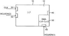
図1は、複数の部分に分割されたプロセッサ・コア10を示しており、一方の部分12が標準データ処理部分、他方の部分が直接メモリ・インターフェイス(direct memory interface)(DMA)30である。プロセッサ・コア10は、プロセッサ・クロック信号(processor clocking signal)CLKを受信するクロック信号入力20、及びバスを介してコアに関連付けられているメモリに接続されるように動作可能である少なくとも1つの読み取り/書き込みポート40を有する。コアは、クロック・イネーブル信号HCLKEN(1)を受信するメモリ・アクセス・イネーブル信号入力60、及びクロック・イネーブル信号HCLKEN(2)を受信するプロセッサ・イネーブル入力50のさらに2つの入力も有し得る。一部の実施例では、プロセッサ・イネーブル信号HCLKEN(2)は、外部信号として受信されるのではなく、コア内のロジックを処理することによって生成される(図3参照)。コアの処理部分12は、HCLKEN(2)信号があらかじめ定められた値を有しているとき、つまりこの実施例では1であるとき、プロセッサ・クロック信号CLKによってクロック制御される。HCLKEN(2)信号が0のとき、処理部分は、プロセッサ・クロック信号CLKを受信せず、したがって非アクティブである。
FIG. 1 shows a
また、コアの直接メモリ・インターフェイス部分30も、プロセッサ・クロック信号CLKによってクロック制御される。メモリ・アクセス・イネーブル信号HCLKEN(1)があらかじめ定められた値、つまりこの実施例では1を有しているとき、直接メモリ・インターフェイス部分は、単にこのCLK信号を受信するだけである。HCLKEN(1)がゼロの場合、メモリ・アクセス・インターフェイス30は、プロセッサ・クロック信号CLKを受信せず、したがって非アクティブである。
The core direct
図2は、本発明の一実施例によるデータ処理装置を示しており、このデータ処理装置は、図1に示すようなデータ・プロセッサ・コア10、命令メモリ70、直接メモリ・アクセス・コントローラ(DMAC)80、及びフラッシュ・メモリ90を有する。プロセッサ・コアは、データ・バス75によって命令メモリ70に接続されている。命令メモリ70は、密結合メモリであり、したがってメモリとコアとの間のデータ転送は常に、予測できるある時間がかかる。
FIG. 2 shows a data processing apparatus according to an embodiment of the present invention, which includes a
DMAC80は、DMAインターフェイス30を介して、外部データ・ソース、この場合はフラッシュ・メモリ90と、コアに関連付けられているメモリ、この場合は命令メモリ70との間のデータの転送を制御する。この実施例では、外部データ・ソースは、プロセッサに関連付けられているフラッシュ・メモリであるが、本発明の実施例は、他の任意の外部データ・ソースと、プロセッサに関連付けられているメモリとの間でデータを転送することができる。示した実施例では、データは、DMAインターフェイス30を介してフラッシュ・メモリ90と命令メモリ70との間で転送される。これは、処理部分12がアクティブである間、又はスリープ状態である間、すなわちHCLKEN(2)が1又は0の間に行うことができる。DMACは、転送されるデータに制御信号を追加する。制御信号は、メモリ70内のデータが格納されている(格納される)場所のアドレスを示し、1つの信号は、データ転送が読み取りであるか書き込みであるかを示す。
The
フラッシュ・メモリ又は他の外部データ・ソースがAMBAバスを介してプロセッサ・コアに接続される一部の実施例では、データを、AMBAバス55を介して直接DMAインターフェイスに送信することができ、DMAC80は必要ない。これは、バスがDMAインターフェイスによって理解されるプロトコルを有しているときに可能であり、したがって、必要なアドレス及び制御信号は、転送されるデータにすでに関連付けられており、DMACによるこれらの信号の追加は必要ない。
In some embodiments where flash memory or other external data source is connected to the processor core via the AMBA bus, the data can be sent directly to the DMA interface via the
DMAインターフェイス30は、プロセッサ・クロック信号CLKによってクロック制御され、各クロック・サイクルで、データ項目及びその対応するアドレスがDMAインターフェイスに入力される。次いでこれらは、レジスタに格納され、次のクロック・サイクルで、読み取り/書き込みポート40を介してデータ・バス75に沿って命令メモリ70に出力される。
The
図2のデータ処理装置の動作の一例は起動時である。この実施例では、データ・プロセッサの起動コードは、フラッシュ・メモリ90に格納される。フラッシュ・メモリはかなり遅いメモリであり、したがってこのコードは、実行前により速い命令メモリ70に転送される。起動が行われる前、プロセッサ・コアは非アクティブであり、起動要求の受信後に、DMAC80は、フラッシュ・メモリ90から起動コードを読み取り、入力42を介してデータをDMAインターフェイスに渡す。この時点で、メモリ・アクセス・イネーブル信号HCKLEN(1)は1に設定され、したがってDMAインターフェイスは、DMACから渡されたデータ項目を読み取り、DMAインターフェイスはプロセッサ・クロックによってクロック制御される。このデータはDMAインターフェイス30を通過し、次いで読み取り/書き込みポート40、及びプロセッサ・コアのデータ・バス75を介して命令メモリ70に出力される。この実施例では、コアはスリープ状態(コアのデータ処理部分へのクロック制御はオフにされ、割り込み待ちモード(wait−for−interrupt mode)になっている)であり、したがってDMAインターフェイス30は、コア自体からのデータ転送との任意の潜在的な衝突無しにコアをメモリに接続するデータ・バスを使用することができる。
An example of the operation of the data processing apparatus of FIG. In this embodiment, the data processor activation code is stored in
図3は、図1に示したものに似たプロセッサ・コアを示しており、この実施例では、プロセッサ・イネーブル信号は、外部信号としてコアに入力されるのではなく、処理ロジック52によって生成される。この処理ロジックは、コアのシステム・コントローラの状態の監視に応答して処理イネーブル信号を生成する。処理イネーブル信号及びプロセッサ・クロック信号は、ANDゲートを通過し、ANDゲートの出力は、プロセッサ・コアの処理部分12をクロック制御するために使用される。したがって、処理イネーブル信号が1の場合、プロセッサ・クロック信号CLKは、処理部分12によって受信され、処理イネーブル信号がゼロの場合、クロック信号は受信されず、したがってコアの処理部分は非アクティブ又はスリープ状態である。スリープ・モードでは、コアは、外部ピンでの割り込み要求又はデバッグ要求についてサンプリングを行い、これらのうちのいずれかを受信すると、プロセッサ・イネーブル信号が処理ロジック52によって生成され、割り込み待ちモード(すなわちスリープ・モード)を終了すべきであることをプロセッサ・コアに示す。
FIG. 3 shows a processor core similar to that shown in FIG. 1, in which the processor enable signal is generated by processing
また、図3は、図1のコア10の直接メモリ・アクセス・インターフェイス部分30をより詳しく示している。DMAインターフェイス30は、いくつかのレジスタ32を含み、それぞれ、外部データ・ソースから転送され、入力24を介してコアに入力されるデータ、又はメモリから転送され、バス75を介して読み取り/書き込みポート40に入力されるデータを保持するように動作可能である。このデータは、レジスタ32で保持され、次いで外部データ・ソース又はメモリに転送される。直接メモリ・アクセス・インターフェイス30は、プロセッサ・クロックとメモリ・インターフェイス・イネーブル信号HCLKEN(1)との論理積演算を行うように動作可能であるANDゲート34も含む。レジスタへの格納を含むデータ転送の処理は、ANDゲート34から出力された信号を介してクロック制御される。ANDゲート34は、プロセッサ・クロック信号CLKを一方の入力として、またメモリ・アクセス・インターフェイス・イネーブル信号HCLKEN(1)を他方の入力として受信する。したがって、メモリ・アクセス・インターフェイス・イネーブル信号が実行可能であるとき、すなわち1のとき、プロセッサ・クロックは、ANDゲート34の出力に存在し、したがって直接メモリ・アクセス・インターフェイスは、クロック制御され、アクティブであり、レジスタ32は、データを受信し、転送することができる。HCLKEN(1)が0のとき、クロック信号は受信されず、メモリ・アクセス・インターフェイス30は非アクティブである。転送されたデータは、データ項目、データ項目に関連付けられているアドレス、及びデータがそのアドレスから読み取られるか、そこに書き込まれるかを表す制御信号を含む。これらは一般に、AMBAプロトコルに従って並行してレジスタ32に転送される。
FIG. 3 also shows the direct memory
図4は、2つのクロック信号を受信する直接メモリ・アクセス・インターフェイスのANDゲート34を示している。明らかなように、この実施例では、クロック・イネーブル信号は、定常信号(steady signal)ではなく、むしろクロック信号自体である。これによってANDゲート34は、その出力にプロセッサ・クロックに対して異なる周波数のクロック信号を生成することになる。メモリ・アクセス・インターフェイス30によって実行されるデータ転送をクロック制御するのがこの信号である。これは、プロセッサ・クロックのクロック速度で動作することができない低速メモリからデータが転送されているときに有利である。このようにより遅いクロックを提供する能力は、低速メモリに関連付けられている潜在的な問題を軽減するのに効率的で簡単な方法であり、これによって実際に、より遅いメモリに適した速度でデータ転送を行うことができるようになる。
FIG. 4 shows an AND
データ処理コアの別の処理部分と同じ時にアクティブであり得るメモリ・アクセス・インターフェイス30を有する1つの潜在的な問題は、これらはいずれも、同じときに読み取り/書き込みポート40を介してデータ・アクセスを要求する場合があることである。図5は、これを扱う方法を示している。この実施例では、読み取り/書き込みポート40に関連付けられているアービトレーション・ロジック110が提供され、アービトレーション・ロジックは、2つのデータ・アクセス要求が同じクロック・サイクルで受信されたときに、最初にどのデータ・アクセス要求が処理されるかを制御する。直接メモリ・インターフェイス30は、高速データ転送を提供するために設けられているため、アービトレーション110は、処理部分12から受信された要求より常にDMAデータ・アクセス要求に高い優先順位を与えるように設定される。これに関する1つの潜在的な問題は、大きいデータ転送要求が外部データ・ソースから受信された場合、バス75はしばらくの間DMAインターフェイス30によって独占される可能性があり、したがって、バス75に沿ってメモリにアクセスする必要がある重要なコードを実行する必要がある処理部分12が長時間の停止を被ることである。この問題は、いくつかの実施例では、読み取り/書き込みポート40を複数のデータ・バスに取り付けることができるようにすることによって対処されている。図5は、読み取り/書き込みポート40が3つのバス、75A、75B、及び75Cに接続されているところを示している。
One potential problem with the
この実施例では、密結合メモリ120(図6参照)が3つの部分に分割される。部分120aは、偶数アドレスを有するデータを格納するように動作可能であり、部分120bは、奇数アドレスを有するデータを格納するように動作可能であり、部分120cは、命令を格納するように動作可能である。データ・バス75aは、読み取り/書き込みポート40をメモリ120aの偶数データ部分に接続し、バス75bは、読み取り/書き込みポートをメモリ120bの奇数データ部分に接続し、バス75cは、読み取り/書き込みポートをメモリ120cの命令部分に接続する。このように、密結合メモリ120への可能な経路が3つあり、これらは、同じクロック・サイクル中に並行して使用することができる。これによって、すべての場合に、直接メモリ・アクセス・インターフェイス30からのデータ・アクセス要求に優先順位が与えられたとき、データ・プロセッサ・コア10の処理部分12に起こり得るデータの長時間の停止状態の問題が軽減される。
In this embodiment, the tightly coupled memory 120 (see FIG. 6) is divided into three parts. Portion 120a is operable to store data having even addresses, portion 120b is operable to store data having odd addresses, and portion 120c is operable to store instructions It is. Data bus 75a connects read /
アービトレーション・ロジック110は、どの要求に優先順位が与えられるかを制御し、また適切なバスへのデータ・アクセス要求の経路設定も制御する。これを行うには、データに関連付けられているアドレスを監視し、次いでこのアドレスを含むメモリ120の部分にアクセスするよう動作可能なバスにデータを置く。メモリ120cの命令部分は一般に命令を格納するために使用されるが、命令がそれに関連付けられているデータを有している場合、データ項目を命令とともに配置することができることに留意されたい。データの経路設定は、転送されているデータの種類の検出によるのではなく、データに関連付けられているアドレスを使用して行われる。
信号の経路設定を制御すること、及びDMAインターフェイス30からのデータ・アクセス要求に優先順位を与えることに加えて、コードから出力され、プロセッサ・クロックCLKでクロック制御されているデータ・アクセス要求について行けないほど遅すぎるメモリのときは、アービトレーション・ロジック110を使用して、メモリの部分から出力される待機信号を検出することもできる。この場合、アービトレーション・ロジック110は、待機信号が検出されなくなるまで、他の任意のデータ・アクセス要求を処理しない。
In addition to controlling signal routing and prioritizing data access requests from the
図6は、プロセッサ・コア10に関連付けられている密結合メモリ120をより詳しく示している。明らかなように、メモリはいくつかの部分に分割されており、偶数アドレスが部分120aにマップされ、奇数アドレスが部分120bにマップされる。この実施例では、メモリを語境界でインターリーブ動作させる。命令は部分120cに格納される。このように偶数アドレス及び奇数アドレスを使用したデータのマッピングは、隣接するアドレスを有するいくつかのデータ項目が、交互のバス120a及び120bを使用して連続してアクセスされることを意味する。これは、メモリの特定の部分へのバスのうちの1つが大量のシリアル・データ・アクセス要求によって独占されている確率が低く、したがってコアの処理部分に対してデータの長時間の停止状態が起こる可能性が低いことを意味する。
FIG. 6 shows the tightly coupled
図7は、アービトレーション・ロジック110が同じクロック・サイクルで受信された処理部分12及びDMAインターフェイスからのデータ・アクセス要求をどのように扱うかを概略的に示しているフロー図である。明らかなように、アービトレーション・ロジックは、これらの要求がメモリの同じ部分のアドレスにアクセスしているかどうかを確認し、そうでない場合、それらはそれぞれのバスに沿って並行して経路設定される。それらが同じメモリ部分のアドレスを含んでいる場合、DMAインターフェイスからのデータ・アクセス要求2が最初に経路設定され、次のクロック・サイクルで、処理部分からのデータ・アクセス要求1が経路設定される。
FIG. 7 is a flow diagram that schematically illustrates how the
本発明の実施例について、添付の図面を参照して本明細書で詳しく説明してきたが、本発明は、こうした正確な実施例に限定されるものではなく、添付の特許請求の範囲によって定義された本発明の範囲及び意図から逸脱することなく、当業者によって様々な変更及び修正をそれに加えることができることを理解されたい。例えば、本発明の範囲から逸脱することなく頭記の従属クレームの特徴を独立クレームの特徴と様々に組み合わせることができる。 While embodiments of the present invention have been described in detail herein with reference to the accompanying drawings, the present invention is not limited to these precise embodiments and is defined by the appended claims. It should be understood that various changes and modifications can be made thereto by those skilled in the art without departing from the scope and spirit of the present invention. For example, the features of the dependent claims described above can be variously combined with the features of the independent claims without departing from the scope of the invention.
10 プロセッサ・コア
12 一方の部分
20 クロック信号入力
30 直接メモリ・インターフェイス
32 レジスタ
34 ANDゲート
40 読み取り/書き込みポート
42 入力
50 プロセッサ・イネーブル入力
55 AMBAバス
60 アクセス・イネーブル信号入力
70 命令メモリ
75A データ・バス
75B データ・バス
75C データ・バス
80 直接メモリ・アクセス・コントローラ(DMAC)
90 フラッシュ・メモリ
110 アービトレーション・ロジック
120 密結合メモリ
10
90
Claims (14)
データ・プロセッサ・コアと
を備えたデータ処理装置であって、
前記データ・プロセッサ・コアが
外部データ・ソースとデータ・プロセッサ・コアに関連付けられている少なくとも1つのメモリとの間でデータ転送操作を実行するように動作可能なメモリ・アクセス・インターフェイス部分と、
データ処理操作を実行するように動作可能なデータ処理部分と、
前記プロセッサ・コアから少なくとも2つのバスにデータを転送するように動作可能な読み取り/書き込みポートであって、前記少なくとも2つのバスが前記プロセッサ・コアと前記少なくとも1つのメモリとの間にデータ通信を提供するように動作可能であり、前記少なくとも1つのメモリが少なくとも2つの部分を含み、前記少なくとも2つのバスのそれぞれが前記少なくとも2つの部分のそれぞれにデータ・アクセスを提供するように動作可能である読み取り/書き込みポートと
を含み、
前記アービトレーション・ロジックは前記読み取り/書き込みポートに関連付けられており、前記アービトレーション・ロジックが、前記メモリ・アクセス・インターフェイスから受信された前記少なくとも1つのメモリの一部にあるデータのアクセスを要求するデータ・アクセス要求を、前記少なくとも1つのメモリの前記一部にアクセスを提供する前記少なくとも2つのバスのうちの一方に経路設定し、前記データ処理部分から受信された前記少なくとも1つのメモリの別の一部にあるデータのアクセスを要求する別のデータ・アクセス要求を、前記少なくとも1つのメモリの前記別の一部にアクセスを提供する前記少なくとも2つのバスのうちのもう一方に経路設定するように動作可能であり、前記データ・アクセス要求の前記経路設定が同じクロック・サイクル中に実行され、
前記メモリの前記少なくとも2つの部分が、命令を格納するように動作可能である命令部分、及びデータ項目を格納するように動作可能である少なくとも1つのデータ部分を含み、前記アービトレーション・ロジックは、転送すべきデータが命令であるとき、前記命令部分へのアクセスを提供する前記少なくとも2つのバスのうちの第1のものに前記アクセス要求を経路設定し、転送すべきデータがデータ項目であるとき、前記少なくとも1つのデータ部分へのアクセスを提供する前記少なくとも2つのバスのうちの第2のものに前記データ・アクセス要求を経路設定するように動作可能であり、
前記少なくとも1つのデータ部分が、偶数アドレスを有するデータを格納するように動作可能な偶数データ部分、及び奇数アドレスを有するデータを格納するように動作可能な奇数データ部分の2つのデータ部分を含み、前記読み取り/書き込みポートが、前記命令部分へのアクセスを提供する第1のバス、前記奇数データ部分へのアクセスを提供する第2のバス、及び前記偶数データ部分へのアクセスを提供する第3のバスの3つのバスを介して前記プロセッサ・コアと前記少なくとも1つのメモリとの間にデータを転送するように動作可能であり、前記アービトレーション・ロジックが、転送すべきデータが命令であるときは前記第1のバスに、転送すべきデータが奇数アドレスに関連付けられているデータ項目であるときは前記第2のバスに、転送すべきデータが偶数アドレスに関連付けられているデータ項目であるときは前記第3のバスにデータ・アクセス要求を経路設定するように動作可能である
データ処理装置。 Arbitration logic and
A data processing device comprising a data processor core,
A memory access interface portion operable to cause the data processor core to perform data transfer operations between an external data source and at least one memory associated with the data processor core;
A data processing portion operable to perform data processing operations;
A read / write port operable to transfer data from the processor core to at least two buses, the at least two buses providing data communication between the processor core and the at least one memory. Operable to provide, wherein the at least one memory includes at least two portions, each of the at least two buses being operable to provide data access to each of the at least two portions. Including read / write ports and
The arbitration logic is associated with the read / write port, the arbitration logic requesting access to data in a portion of the at least one memory received from the memory access interface. Another portion of the at least one memory received from the data processing portion that routes an access request to one of the at least two buses that provides access to the portion of the at least one memory Operable to route another data access request requesting access to data at the other of the at least two buses providing access to the another portion of the at least one memory And the routing of the data access request There are performed during the same clock cycle,
The at least two portions of the memory include an instruction portion operable to store an instruction and at least one data portion operable to store a data item; When the data to be transmitted is an instruction, the access request is routed to a first one of the at least two buses providing access to the instruction portion, and the data to be transferred is a data item; Operable to route the data access request to a second of the at least two buses providing access to the at least one data portion;
The at least one data portion includes two data portions, an even data portion operable to store data having even addresses and an odd data portion operable to store data having odd addresses; The read / write port provides a first bus that provides access to the instruction portion, a second bus that provides access to the odd data portion, and a third bus that provides access to the even data portion. Operable to transfer data between the processor core and the at least one memory via three buses, wherein the arbitration logic is configured to transfer the data when the data to be transferred is an instruction. When the data to be transferred to the first bus is a data item associated with an odd address, the second bus The scan, the data processing apparatus when the data to be transferred is a data item that is associated with the even address is operable to route the data access request to said third bus.
少なくとも2つの部分に分割される少なくとも1つのメモリと、
前記少なくとも1つのメモリの前記少なくとも2つの部分のそれぞれの部分へのデータ・アクセスをそれぞれ可能にする少なくとも2つのバスと
を含むデータ処理装置。 The data processing apparatus of claim 1, further comprising at least one memory divided into at least two parts;
A data processing apparatus comprising: at least two buses each enabling data access to a respective part of said at least two parts of said at least one memory.
前記メモリ・アクセス・インターフェイス部分から受信された前記少なくとも1つのメモリの一部にあるデータのアクセスを要求するデータ・アクセス要求、及び前記データ処理部分から受信された前記少なくとも1つのメモリの別の部分にあるデータへのアクセスを要求するデータ・アクセス要求に応答して、前記メモリ・アクセス・インターフェイス部分から受信された前記データ・アクセス要求を少なくとも2つのバスのうちの一方に経路設定するステップであって、前記少なくとも2つのバスのうちの前記一方が前記少なくとも1つのメモリの前記一部へのアクセスを提供するステップと、前記データ処理部分から受信された前記データ・アクセス要求を前記少なくとも2つのバスのうちのもう一方のバスに経路設定するステップであって、前記別のバスが前記少なくとも1つのメモリの前記別の部分へのアクセスを提供するステップとを含み、前記データ・アクセス要求の前記経路設定が同じクロック・サイクル中に実行され、
前記メモリの前記少なくとも2つの部分が、命令を格納するように動作可能である命令部分、及びデータ項目を格納するように動作可能である少なくとも1つのデータ部分を含み、前記データ・アクセス要求を経路設定する前記ステップが、転送すべきデータが命令であるとき、前記命令部分へのアクセスを提供する前記少なくとも2つのバスのうちの一方にデータ・アクセス要求を経路設定し、転送すべきデータがデータ項目であるとき、前記少なくとも1つのデータ部分へのアクセスを提供する前記少なくとも2つのバスのうちのもう一方に前記データ・アクセス要求を経路設定するように動作可能であり、
前記少なくとも1つのデータ部分が、偶数アドレスを有するデータを格納するように動作可能な偶数データ部分、及び奇数アドレスを有するデータを格納するように動作可能な奇数データ部分の2つのデータ部分を含み、前記経路設定するステップが、前記命令部分へのアクセスを提供する第1のバス、前記奇数データ部分へのアクセスを提供する第2のバス、及び前記偶数データ部分へのアクセスを提供する第3のバスの3つのバスのうちの1つにデータ・アクセスを経路設定するように動作可能であり、前記経路設定するステップが、転送すべきデータが命令であるときは前記第1のバスに、転送すべきデータが奇数アドレスに関連付けられているデータ項目であるときは前記第2のバスに、転送すべきデータが偶数アドレスに関連付けられているデータ項目であるときは前記第3のバスにデータ・アクセス要求を経路設定するように動作可能である
方法。 A method of transferring data between an external data source and at least one memory associated with a data processor core, the data processor core comprising the external data source and the data processor A memory access interface portion operable to perform data transfer operations to and from the at least one memory associated with the core, and data processing operable to perform data processing operations A data access request for requesting access to data in a portion of the at least one memory received from the memory access interface portion, and the at least received from the data processing portion. Access to data in another part of one memory Routing the data access request received from the memory access interface portion to one of at least two buses in response to a requesting data access request, the at least two buses Said one of the at least one memory providing access to said portion of said at least one memory, and said data access request received from said data processing portion is transmitted to the other bus of said at least two buses And wherein said another bus provides access to said another portion of said at least one memory, wherein said routing of said data access request is during the same clock cycle is executed,
The at least two portions of the memory include an instruction portion operable to store an instruction and at least one data portion operable to store a data item, wherein the data access request is routed The step of setting, when the data to be transferred is an instruction, routes a data access request to one of the at least two buses providing access to the instruction part, and the data to be transferred is data An item is operable to route the data access request to the other of the at least two buses providing access to the at least one data portion;
The at least one data portion includes two data portions, an even data portion operable to store data having even addresses and an odd data portion operable to store data having odd addresses; The routing step provides a first bus that provides access to the instruction portion, a second bus that provides access to the odd data portion, and a third bus that provides access to the even data portion. Operable to route data access to one of the three buses, wherein the routing step transfers to the first bus when the data to be transferred is an instruction When the data to be transmitted is a data item associated with an odd address, the data to be transferred is associated with the even address. The method is operable to route the data access request to said third bus when a data item being.
Applications Claiming Priority (1)
| Application Number | Priority Date | Filing Date | Title |
|---|---|---|---|
| US10/815,961 US7240144B2 (en) | 2004-04-02 | 2004-04-02 | Arbitration of data transfer requests |
Publications (3)
| Publication Number | Publication Date |
|---|---|
| JP2005293596A JP2005293596A (en) | 2005-10-20 |
| JP2005293596A5 JP2005293596A5 (en) | 2007-08-30 |
| JP4642531B2 true JP4642531B2 (en) | 2011-03-02 |
Family
ID=34574887
Family Applications (1)
| Application Number | Title | Priority Date | Filing Date |
|---|---|---|---|
| JP2005106228A Active JP4642531B2 (en) | 2004-04-02 | 2005-04-01 | Arbitration of data requests |
Country Status (3)
| Country | Link |
|---|---|
| US (1) | US7240144B2 (en) |
| JP (1) | JP4642531B2 (en) |
| GB (1) | GB2412767B (en) |
Families Citing this family (6)
| Publication number | Priority date | Publication date | Assignee | Title |
|---|---|---|---|---|
| US8510491B1 (en) * | 2005-04-05 | 2013-08-13 | Oracle America, Inc. | Method and apparatus for efficient interrupt event notification for a scalable input/output device |
| CN101118523B (en) * | 2006-08-01 | 2011-10-19 | 飞思卡尔半导体公司 | Memory accessing control device and method thereof, and memory accessing controller and method thereof |
| US9015720B2 (en) * | 2008-04-30 | 2015-04-21 | Advanced Micro Devices, Inc. | Efficient state transition among multiple programs on multi-threaded processors by executing cache priming program |
| US20120102242A1 (en) * | 2010-10-26 | 2012-04-26 | Kaminario Technologies Ltd. | Controlling data destaging within a multi-tiered storage system |
| FR2986345B1 (en) * | 2012-01-27 | 2014-02-28 | Simpulse | METHOD FOR MANAGING MEMORY ACCESS REQUESTS AND DATA STORAGE SYSTEM |
| US10599208B2 (en) | 2015-09-08 | 2020-03-24 | Toshiba Memory Corporation | Memory system and controller |
Citations (6)
| Publication number | Priority date | Publication date | Assignee | Title |
|---|---|---|---|---|
| JPH10509540A (en) * | 1994-10-04 | 1998-09-14 | アナログ・デバイセス・インコーポレーテッド | Digital signal processor |
| JP2000163312A (en) * | 1998-12-01 | 2000-06-16 | Fujitsu Ltd | Microprocessor |
| JP2000215187A (en) * | 1999-01-01 | 2000-08-04 | Seiko Epson Corp | Multiprocessor system |
| JP2000235560A (en) * | 1999-02-16 | 2000-08-29 | Hitachi Ltd | Microcomputer and microcomputer system |
| JP2003140964A (en) * | 2001-11-05 | 2003-05-16 | Denso Corp | Data processing system |
| JP2004062900A (en) * | 2002-07-29 | 2004-02-26 | Samsung Electronics Co Ltd | Memory controller for increasing bas band width, data transmission method using the same and computer system having the same |
Family Cites Families (53)
| Publication number | Priority date | Publication date | Assignee | Title |
|---|---|---|---|---|
| NO173304C (en) * | 1984-12-20 | 1993-11-24 | Honeywell Inc | Double bus system |
| US4744006A (en) * | 1986-07-10 | 1988-05-10 | Duffield Robert H | Apparatus for expanding the input/output capabilities of a personal computer |
| JPS63236153A (en) * | 1987-03-24 | 1988-10-03 | Nec Corp | Storage device |
| US4979100A (en) * | 1988-04-01 | 1990-12-18 | Sprint International Communications Corp. | Communication processor for a packet-switched network |
| US5191573A (en) * | 1988-06-13 | 1993-03-02 | Hair Arthur R | Method for transmitting a desired digital video or audio signal |
| US5184282A (en) * | 1989-02-27 | 1993-02-02 | Mips Co., Ltd. | IC card adapter |
| DE3912605B4 (en) * | 1989-04-17 | 2008-09-04 | Fraunhofer-Gesellschaft zur Förderung der angewandten Forschung e.V. | Digital coding method |
| CA2017471C (en) * | 1989-07-19 | 2000-10-24 | Matthew Eric Krisl | Optical interference coatings and lamps using same |
| JP2860362B2 (en) * | 1990-03-17 | 1999-02-24 | アムフェノル―トゥヘル、エレクトロニクス、ゲゼルシャフト、ミット、ベシュレンクテル、ハフツング | Contact devices, especially contact devices for subscriber identification modules |
| US5049728A (en) * | 1990-04-04 | 1991-09-17 | Rovin George H | IC card system with removable IC modules |
| US5663901A (en) * | 1991-04-11 | 1997-09-02 | Sandisk Corporation | Computer memory cards using flash EEPROM integrated circuit chips and memory-controller systems |
| US5291584A (en) * | 1991-07-23 | 1994-03-01 | Nexcom Technology, Inc. | Methods and apparatus for hard disk emulation |
| US5566290A (en) * | 1992-04-29 | 1996-10-15 | Canon Kabushiki Kaisha | Multi-media device |
| EP0620933A4 (en) * | 1992-11-12 | 1995-03-01 | New Media Corp | Reconfigureable interface between a computer and peripheral devices. |
| JPH0737049A (en) * | 1993-07-23 | 1995-02-07 | Toshiba Corp | External storage |
| US5887145A (en) * | 1993-09-01 | 1999-03-23 | Sandisk Corporation | Removable mother/daughter peripheral card |
| FR2710996B1 (en) * | 1993-10-06 | 1995-12-01 | Gemplus Card Int | Multi-application portable card for personal computer. |
| US5519577A (en) * | 1993-12-23 | 1996-05-21 | Symbol Technologies, Inc. | Spread spectrum radio incorporated in a PCMCIA Type II card holder |
| US5491774A (en) * | 1994-04-19 | 1996-02-13 | Comp General Corporation | Handheld record and playback device with flash memory |
| US5664231A (en) * | 1994-04-29 | 1997-09-02 | Tps Electronics | PCMCIA interface card for coupling input devices such as barcode scanning engines to personal digital assistants and palmtop computers |
| US5545057A (en) * | 1994-05-27 | 1996-08-13 | Hon Hai Precision Ind. Co., Ltd. | Interconnection system with I/O connector module board |
| US5577230A (en) * | 1994-08-10 | 1996-11-19 | At&T Corp. | Apparatus and method for computer processing using an enhanced Harvard architecture utilizing dual memory buses and the arbitration for data/instruction fetch |
| US5611055A (en) * | 1994-09-27 | 1997-03-11 | Novalink Technologies | Method and apparatus for implementing a PCMCIA auxiliary port connector for selectively communicating with peripheral devices |
| US5611057A (en) * | 1994-10-06 | 1997-03-11 | Dell Usa, L.P. | Computer system modular add-in daughter card for an adapter card which also functions as an independent add-in card |
| US5619396A (en) * | 1995-02-21 | 1997-04-08 | Intel Corporation | Modular PCMCIA card |
| US5818030A (en) * | 1995-03-07 | 1998-10-06 | Reyes; Rene A. | Credit card system with key module |
| US5892213A (en) * | 1995-09-21 | 1999-04-06 | Yamaichi Electronics Co., Ltd. | Memory card |
| DE29518707U1 (en) * | 1995-11-25 | 1996-01-18 | Stocko Metallwarenfab Henkels | Contact unit for card-shaped carrier elements of electronic assemblies |
| US5661635A (en) * | 1995-12-14 | 1997-08-26 | Motorola, Inc. | Reusable housing and memory card therefor |
| JP2721329B2 (en) * | 1995-12-28 | 1998-03-04 | 山一電機株式会社 | Card-in type connector |
| US5787445A (en) * | 1996-03-07 | 1998-07-28 | Norris Communications Corporation | Operating system including improved file management for use in devices utilizing flash memory as main memory |
| FR2747847B1 (en) * | 1996-04-18 | 1998-07-03 | Itt Composants Instr | ELECTRONIC CONNECTION BOX, TO A PERSONAL COMPUTER, EQUIPPED WITH A CONNECTOR FOR A CHIP CARD |
| US5752857A (en) * | 1996-05-24 | 1998-05-19 | Itt Corporation | Smart card computer adaptor |
| TW332334B (en) * | 1996-05-31 | 1998-05-21 | Toshiba Co Ltd | The semiconductor substrate and its producing method and semiconductor apparatus |
| JPH09327990A (en) * | 1996-06-11 | 1997-12-22 | Toshiba Corp | Card type storing device |
| EP0833268A3 (en) * | 1996-09-20 | 1999-01-20 | Siemens Aktiengesellschaft | Card reading device |
| JP3585336B2 (en) * | 1997-02-24 | 2004-11-04 | 沖電気工業株式会社 | IC card adapter |
| JPH10302030A (en) * | 1997-02-28 | 1998-11-13 | Toshiba Corp | Connection device and information processor |
| JPH10254767A (en) * | 1997-03-10 | 1998-09-25 | Sharp Corp | Memory controller and memory system by the controller |
| US5876218A (en) * | 1997-05-28 | 1999-03-02 | Gateway 2000, Inc. | Piggy back PC card |
| US5879007A (en) * | 1997-11-12 | 1999-03-09 | Kasri; Omar | Simplified game of chance and skill |
| US5928347A (en) * | 1997-11-18 | 1999-07-27 | Shuttle Technology Group Ltd. | Universal memory card interface apparatus |
| US6102714A (en) * | 1998-03-02 | 2000-08-15 | 3Com Corporation | Electrical connectors having dual biased contact pins |
| KR100278368B1 (en) * | 1998-04-10 | 2001-01-15 | 윤종용 | Portable electronic system having a structure for connecting expansion cards to sockets |
| US5933328A (en) * | 1998-07-28 | 1999-08-03 | Sandisk Corporation | Compact mechanism for removable insertion of multiple integrated circuit cards into portable and other electronic devices |
| US6293464B1 (en) * | 1999-01-05 | 2001-09-25 | Jared Joseph Smalley, Jr. | Card reader |
| US6276943B1 (en) * | 1999-02-22 | 2001-08-21 | Amphenol Corporation | Modular plug connector and improved receptacle therefore |
| US6353870B1 (en) * | 1999-05-11 | 2002-03-05 | Socket Communications Inc. | Closed case removable expansion card having interconnect and adapter circuitry for both I/O and removable memory |
| US6599147B1 (en) * | 1999-05-11 | 2003-07-29 | Socket Communications, Inc. | High-density removable expansion module having I/O and second-level-removable expansion memory |
| JP2001043180A (en) * | 1999-08-03 | 2001-02-16 | Mitsubishi Electric Corp | Microprocessor and storage device therefor |
| US6681283B1 (en) * | 1999-08-12 | 2004-01-20 | Mips Technologies, Inc. | Coherent data apparatus for an on-chip split transaction system bus |
| JP4059473B2 (en) * | 2001-08-09 | 2008-03-12 | 株式会社ルネサステクノロジ | Memory card and memory controller |
| US6931479B2 (en) * | 2003-03-04 | 2005-08-16 | Micron Technology, Inc. | Method and apparatus for multi-functional inputs of a memory device |
-
2004
- 2004-04-02 US US10/815,961 patent/US7240144B2/en active Active
-
2005
- 2005-03-30 GB GB0506399A patent/GB2412767B/en active Active
- 2005-04-01 JP JP2005106228A patent/JP4642531B2/en active Active
Patent Citations (6)
| Publication number | Priority date | Publication date | Assignee | Title |
|---|---|---|---|---|
| JPH10509540A (en) * | 1994-10-04 | 1998-09-14 | アナログ・デバイセス・インコーポレーテッド | Digital signal processor |
| JP2000163312A (en) * | 1998-12-01 | 2000-06-16 | Fujitsu Ltd | Microprocessor |
| JP2000215187A (en) * | 1999-01-01 | 2000-08-04 | Seiko Epson Corp | Multiprocessor system |
| JP2000235560A (en) * | 1999-02-16 | 2000-08-29 | Hitachi Ltd | Microcomputer and microcomputer system |
| JP2003140964A (en) * | 2001-11-05 | 2003-05-16 | Denso Corp | Data processing system |
| JP2004062900A (en) * | 2002-07-29 | 2004-02-26 | Samsung Electronics Co Ltd | Memory controller for increasing bas band width, data transmission method using the same and computer system having the same |
Also Published As
| Publication number | Publication date |
|---|---|
| JP2005293596A (en) | 2005-10-20 |
| GB2412767A (en) | 2005-10-05 |
| GB0506399D0 (en) | 2005-05-04 |
| GB2412767B (en) | 2006-09-06 |
| US20050223129A1 (en) | 2005-10-06 |
| US7240144B2 (en) | 2007-07-03 |
Similar Documents
| Publication | Publication Date | Title |
|---|---|---|
| US4821185A (en) | I/O interface system using plural buffers sized smaller than non-overlapping contiguous computer memory portions dedicated to each buffer | |
| JP3218773B2 (en) | Cache controller | |
| US20060059489A1 (en) | Parallel processing system, interconnection network, node and network control method, and program therefor | |
| JP4642531B2 (en) | Arbitration of data requests | |
| JP2008276391A (en) | Memory access control device | |
| US7165126B2 (en) | Direct memory access device | |
| US5594880A (en) | System for executing a plurality of tasks within an instruction in different orders depending upon a conditional value | |
| US7096307B2 (en) | Shared write buffer in a peripheral interface and method of operating | |
| US7254667B2 (en) | Data transfer between an external data source and a memory associated with a data processor | |
| JPH11232213A (en) | Data transfer system for input/output device | |
| KR920002830B1 (en) | Direct memory access controller | |
| CA2078913A1 (en) | Interprocessor communication system and method for multiprocessor circuitry | |
| US20080209085A1 (en) | Semiconductor device and dma transfer method | |
| EP0437712A2 (en) | Tandem cache memory | |
| JP2009037639A (en) | Dmac issue mechanism via streaming identification method | |
| JP4818820B2 (en) | Bus system, bus slave and bus control method | |
| JPH10283302A (en) | Method and system for supplying data to bus connected to plural processors | |
| JP2005107873A (en) | Semiconductor integrated circuit | |
| JP3077807B2 (en) | Microcomputer system | |
| JP6992616B2 (en) | Data transfer device, data transfer method, program | |
| JP7003752B2 (en) | Data transfer device, data transfer method, program | |
| JPH0962633A (en) | Network control unit | |
| WO2011030498A1 (en) | Data processing device and data processing method | |
| JP2004220309A (en) | Multiprocessor system | |
| JP2632859B2 (en) | Memory access control circuit |
Legal Events
| Date | Code | Title | Description |
|---|---|---|---|
| A521 | Request for written amendment filed |
Free format text: JAPANESE INTERMEDIATE CODE: A523 Effective date: 20070711 |
|
| A621 | Written request for application examination |
Free format text: JAPANESE INTERMEDIATE CODE: A621 Effective date: 20070711 |
|
| A977 | Report on retrieval |
Free format text: JAPANESE INTERMEDIATE CODE: A971007 Effective date: 20100728 |
|
| A131 | Notification of reasons for refusal |
Free format text: JAPANESE INTERMEDIATE CODE: A131 Effective date: 20100803 |
|
| A521 | Request for written amendment filed |
Free format text: JAPANESE INTERMEDIATE CODE: A523 Effective date: 20101026 |
|
| TRDD | Decision of grant or rejection written | ||
| A01 | Written decision to grant a patent or to grant a registration (utility model) |
Free format text: JAPANESE INTERMEDIATE CODE: A01 Effective date: 20101116 |
|
| A01 | Written decision to grant a patent or to grant a registration (utility model) |
Free format text: JAPANESE INTERMEDIATE CODE: A01 |
|
| A61 | First payment of annual fees (during grant procedure) |
Free format text: JAPANESE INTERMEDIATE CODE: A61 Effective date: 20101201 |
|
| R150 | Certificate of patent or registration of utility model |
Ref document number: 4642531 Country of ref document: JP Free format text: JAPANESE INTERMEDIATE CODE: R150 Free format text: JAPANESE INTERMEDIATE CODE: R150 |
|
| FPAY | Renewal fee payment (event date is renewal date of database) |
Free format text: PAYMENT UNTIL: 20131210 Year of fee payment: 3 |
|
| R250 | Receipt of annual fees |
Free format text: JAPANESE INTERMEDIATE CODE: R250 |
|
| R250 | Receipt of annual fees |
Free format text: JAPANESE INTERMEDIATE CODE: R250 |
|
| R250 | Receipt of annual fees |
Free format text: JAPANESE INTERMEDIATE CODE: R250 |
|
| R250 | Receipt of annual fees |
Free format text: JAPANESE INTERMEDIATE CODE: R250 |
|
| R250 | Receipt of annual fees |
Free format text: JAPANESE INTERMEDIATE CODE: R250 |
|
| R250 | Receipt of annual fees |
Free format text: JAPANESE INTERMEDIATE CODE: R250 |
|
| R250 | Receipt of annual fees |
Free format text: JAPANESE INTERMEDIATE CODE: R250 |
|
| R250 | Receipt of annual fees |
Free format text: JAPANESE INTERMEDIATE CODE: R250 |
|
| R250 | Receipt of annual fees |
Free format text: JAPANESE INTERMEDIATE CODE: R250 |
|
| R250 | Receipt of annual fees |
Free format text: JAPANESE INTERMEDIATE CODE: R250 |
|
| R250 | Receipt of annual fees |
Free format text: JAPANESE INTERMEDIATE CODE: R250 |