JP2006302132A - Signal processor, reconfigurable logic circuit device and reconfigurable sequential circuit - Google Patents
Signal processor, reconfigurable logic circuit device and reconfigurable sequential circuit Download PDFInfo
- Publication number
- JP2006302132A JP2006302132A JP2005125451A JP2005125451A JP2006302132A JP 2006302132 A JP2006302132 A JP 2006302132A JP 2005125451 A JP2005125451 A JP 2005125451A JP 2005125451 A JP2005125451 A JP 2005125451A JP 2006302132 A JP2006302132 A JP 2006302132A
- Authority
- JP
- Japan
- Prior art keywords
- logic circuit
- memory
- signal
- unit
- reconfigurable
- Prior art date
- Legal status (The legal status is an assumption and is not a legal conclusion. Google has not performed a legal analysis and makes no representation as to the accuracy of the status listed.)
- Pending
Links
Images


Landscapes
- Logic Circuits (AREA)
Abstract
Description
本発明は、論理回路部に関する回路装置に関し、特に、再構成可能な組み込み系の信号処理装置、及び、定義用のデータを与えて論理回路の構成を変更することが可能な再構成可能論理回路装置、詳しくはクロック単位で論理回路の構成変更を可能にする動的な再構成可能論理回路装置、及び、ディジタル回路における他の回路の動作を制御できる順序回路、等の論理回路部関連の回路装置に関するものである。 The present invention relates to a circuit device related to a logic circuit section, and more particularly to a reconfigurable embedded signal processing device and a reconfigurable logic circuit capable of changing the configuration of a logic circuit by providing definition data. Circuits related to logic circuit units, such as a dynamic reconfigurable logic circuit device that can change the configuration of a logic circuit in units of clocks, and a sequential circuit that can control the operation of other circuits in a digital circuit It relates to the device.
従来の信号処理装置を図19と図20に示す。
従来の信号処理装置は回路規模の小さなハードウェアで、画像処理と、補助的なアクセラレータ機能とを実行できるようにしたものであった。図19において、要求速度で処理できない画像データは演算装置120から演算装置I/F122を経由してノンリアルタイムパス124に送られて処理され、その後、演算装置I/Fを経由して、指定された記憶装置のアドレスに転送される。
転送されたデータは、必要であれば、さらに演算装置で処理され、またはノンリアルタイムパスで繰り返し処理され、またはリアルタイムパス123へ転送され、最終的に出力デバイス126に送られる。要求速度で処理できる画像データは、演算装置I/Fを介して直接にリアルタイムパス123へ送られる。
リアルタイムパスへ送られた画像データは出力デバイスI/F125を経由して出力デバイス126に出力される。図20において、演算装置I/F122は入力バッファ221およびパス決定部222を含む。
ノンリアルタイムパス124は、再構成データ制御部6、論理回路部5、ワークメモリ241、出力バッファ242を含んで構成されている。演算装置120でパスが決定され必要なヘッダ情報を付加した画像データは演算装置I/F122に送られる。演算装置I/Fは画像データを入力バッファ221へ蓄え、ヘッダ情報に書かれたリアルタイム、またはノンリアルタイムの識別に基づいてパス決定部222がデータの送る方向を決める。
ヘッダ情報は再構成データ制御部に送られ、この再構成データ制御部はヘッダ情報に書かれた次に動作させる処理内容を、論理回路部にロードする。入力バッファ221はノンリアルタイムパス124で処理するデータを論理回路部5に送る。論理回路部はワークメモリ241を使用して演算処理しその結果を出力バッファ242に送り、出力バッファはヘッダに書かれたメモリアドレスへ転送する(例えば、特許文献1参照)。従来例の論理回路部は動的に書き換え可能なFPGA(Field Programable Gate Array)素子で構成しており、このように、従来の信号処理装置は、ヘッダ情報の解析後に論理回路部を実行させるのである。更に、リアルタイムを必要としない分野での利用となる。
A conventional signal processing apparatus is shown in FIGS.
The conventional signal processing apparatus is a hardware having a small circuit scale and can execute image processing and an auxiliary accelerator function. In FIG. 19, image data that cannot be processed at the requested speed is sent from the arithmetic unit 120 to the non-real-time path 124 via the arithmetic unit I / F 122 and processed, and then designated via the arithmetic unit I / F. To the address of the storage device.
If necessary, the transferred data is further processed by the arithmetic unit, or repeatedly processed by the non-real time path, or transferred to the real time path 123 and finally sent to the output device 126. Image data that can be processed at the required speed is sent directly to the real-time path 123 via the arithmetic unit I / F.
The image data sent to the real-time path is output to the output device 126 via the output device I / F 125. In FIG. 20, the arithmetic unit I / F 122 includes an input buffer 221 and a path determination unit 222.
The non-real time path 124 includes a reconfiguration data control unit 6, a
The header information is sent to the reconfiguration data control unit, and the reconfiguration data control unit loads the processing contents to be operated next written in the header information into the logic circuit unit. The input buffer 221 sends data to be processed through the non-real time path 124 to the
また、従来の再構成可能論理回路装置は、図21に示すように、定義用データに応じて内部論理要素の接続関係が特定される論理回路部13と、この論理回路部に与える定義用データを格納する定義用メモリ部12とを備え、定義用メモリ部は、2つの揮発性メモリおよびと、揮発性メモリおよびのいずれか一方から定義用データを選択的に論理回路部にロードする選択制御手段とを備えている。このように、定義用メモリとして揮発性メモリをセットで有するので、選択制御手段で揮発性メモリの選択の切り換えを行うだけで、論理回路部にロードする定義用データを変更できるようにしている(特許文献2参照)。
このように、従来の再構成可能論理回路装置は、定義用データを複数もち、それを切り換えて読み出しを行なうことで、論理回路部13の機能変更を行なうのである。
また、従来の再構成可能順序回路を図22に示す。
逐次読み出しを繰り返し行うことが可能なメモリ100と、該メモリ100から逐次読み出された最終内容に対応する内容が現在の状態として設定される状態記憶手段300と、外部入力された遷移条件と、状態記憶手段300の設定内容に応じてメモリ100に逐次読み出しを行わせる遷移条件記憶手段200とで構成している(特許文献3参照)。
このように、従来の再構成可能順序回路は、状態遷移条件の複雑さに影響されない組み合わせ回路によって状態遷移回路を構成するのである。
As described above, the conventional reconfigurable logic circuit device has a plurality of definition data, and changes the function of the logic circuit unit 13 by switching and reading the data.
A conventional reconfigurable sequential circuit is shown in FIG.
A memory 100 capable of repeatedly performing sequential reading, a state storage means 300 in which content corresponding to final content sequentially read from the memory 100 is set as a current state, an externally input transition condition, The transition condition storage means 200 is configured to cause the memory 100 to sequentially read in accordance with the setting contents of the state storage means 300 (see Patent Document 3).
Thus, the conventional reconfigurable sequential circuit configures the state transition circuit by a combinational circuit that is not affected by the complexity of the state transition condition.
しかしながら、特許文献1の信号処理装置は、論理回路部をヘッダ情報の内容を解析した後に起動するため、論理回路部での処理要求から開始までのレーテンシが大きくなるという問題がある。そのためリアルタイム性を必要としない分野でしか利用できないという問題を併せ持つ。
また、論理回路部としてFPGAを利用しているため、再構成データが格納されているメモリのリードと、論理回路部を構成するエレメントの変更を逐次的に行なっていくため、ハードウェアの再構成に数msec以上の時間を要するという問題を持っている。このことは、MHz以上のシステムクロックレベル動作する信号処理装置において、システムクロックレベルでハードウェアの再構成を動的に行うことができず、再構成のためには信号処理装置の動作が停止してしまうという問題もある。
そして、ヘッダ情報の解析処理やFPGAの利用など、信号処理装置のシステムレベルが大規模化するという問題もさらに持っている。
However, since the signal processing device of
In addition, since the FPGA is used as the logic circuit unit, the read of the memory storing the reconfiguration data and the change of the elements constituting the logic circuit unit are sequentially performed. Has a problem that it takes several milliseconds or more. This means that in a signal processing device that operates at a system clock level of MHz or higher, hardware reconfiguration cannot be performed dynamically at the system clock level, and the operation of the signal processing device stops for reconfiguration. There is also the problem of end up.
Further, there is a further problem that the system level of the signal processing device becomes large, such as analysis processing of header information and use of FPGA.
また、特許文献2の再構成可能論理回路装置は、少なくともメモリの出力ポートより大きなサイズの、論理回路部の定義データがメモリに記憶されているため、選択制御器にメモリの読み込み回路と読み込んだ定義データの保持回路が必要である。特に論理回路部のデータは大きいため、定義データの保持回路は回路規模を増加する要因である。機能変更のためには、メモリから定義データを一度読み出しておかなければならないため、クロック単位のダイナミックな定義データの切り換えを行なえないという問題があった。
さらに、定義データの切り換えをCPUで行なっており、装置内にCPUを必ず必要とするという問題があった。
また、特許文献3の再構成可能順序回路では、状態遷移のみが再構成可能であった。そのため、出力信号は状態であり、受け側の回路において状態の解釈の必要が生ずる。このことは順序回路で制御される回路がIPで提供されても再設計が生ずるという問題があった。
更に、IPの再設計を行わない場合には、何らかの状態解釈回路を必要とするため、個別に回路を必要とするという問題があった。同時に入力信号の増減にも対応できていないという問題も併せ持っていた。
その他、入力信号から遷移後の状態を探索するため、入力信号が逐次読出しメモリのアドレスとして利用されていて、状態遷移に不要なメモリの読出し時間が加算されるという問題と、状態と入力信号の組合わせの数でメモリ要領が決定され多くのメモリ容量が要求されるという問題も持っていた。
In the reconfigurable logic circuit device disclosed in
Furthermore, since the definition data is switched by the CPU, there is a problem that the CPU is necessarily required in the apparatus.
Further, in the reconfigurable sequential circuit of
Further, when the IP is not redesigned, some state interpretation circuit is required, so that there is a problem that a separate circuit is required. At the same time, there was a problem that it could not cope with the increase or decrease of the input signal.
In addition, in order to search the state after the transition from the input signal, the input signal is sequentially used as the address of the read memory, and the memory read time unnecessary for the state transition is added, and the state and the input signal The memory procedure is determined by the number of combinations, and a large amount of memory capacity is required.
本発明の第1の発明は、このような問題点に鑑みてなされたものであり、ハードウェアの構成を動的に行い、割込み要求に応じてハードウェアの再構成を行うことによって、動作までのレーテンシが最小となるような信号処理装置を提供することを目的とする。
本発明の第2の発明は、クロック単位で定義データの変更を可能とし、インデックス等により定義データの管理を容易にすると共に、論理回路部の演算結果で自己の回路変更を決定し、LSI化に最適になるように回路規模を抑えることができる再構成可能論理回路装置を提供することを目的とする。
本発明の第3の発明は、回路の再設計を必要とすることなくメモリ容量を抑えることが可能な再構成可能順序回路を提供することを目的とする。
The first invention of the present invention has been made in view of such problems, and by dynamically configuring the hardware and reconfiguring the hardware in response to an interrupt request, the operation can be performed. An object of the present invention is to provide a signal processing apparatus that minimizes the latency.
According to the second aspect of the present invention, definition data can be changed in units of clocks, management of definition data is facilitated by an index or the like, and its own circuit change is determined based on a calculation result of a logic circuit unit, and the LSI is realized. An object of the present invention is to provide a reconfigurable logic circuit device capable of suppressing the circuit scale so as to be optimal.
It is an object of the third invention of the present invention to provide a reconfigurable sequential circuit capable of suppressing the memory capacity without requiring circuit redesign.
上記目的を達成するため、請求項1に記載の発明は、再構成可能な回路装置を備えた信号処理装置において、CPUとメモリ、I/Oデバイス群及び割込みコントローラを有し、前記CPUからアクセス可能なI/Oデバイス群で生成されるn本の割込みソースを入力として、ある割込みソースから論理回路部起動信号を生成し、論理回路部ACK信号とその他の割込みソースから割込みコントローラへの割込み要求を生成する論理回路部起動部と、論理回路部データとして利用するバンクメモリのバンク番号を保持し、バンク番号が変更されると再構成トリガ信号を生成する前記CPUにより設定されるインデックスレジスタと、論理回路部の構成を決定する構成データを記憶するバンク構成のメモリで、選択されたバンクメモリの出力が論理回路部データとして常に前記論理回路部に作用する定義用メモリ部により構成され前記CPUからアクセス可能である再構成データ制御部と、前記CPUからアクセス可能で、前記論理回路部起動信号により演算処理を開始し、演算処理終了後に論理回路部ACK信号を出力し、論理回路部データの内容と再構成トリガ信号に応じてハードウェアの構成を変更する論理回路部と、備えることを特徴としている。
また、請求項2に記載の発明は、請求項1記載の信号処理装置において、前記論理回路部起動部では、CPUからアクセス可能で要求を受け付ける割り込みソースから論理回路部起動信号の生成と、この状態のエンコードデータと前記インデックスレジスタの内容を変更する信号である再構成データ選択信号の生成を行い、前記論理回路部ACK信号と要求を受け付けられていないその他の割り込みソースから、前記割込みコントローラへの割り込み要求の生成を行って、前記インデックスレジスタを前記CPUもしくは再構成データ選択信号で設定するように構成したことを特徴としている。
また、請求項3に記載の発明は、請求項2記載の信号処理装置において、前記論理回路部に、前記再構成データ選択信号と論理回路部データを用いて、論理回路部を実現するための基本要素の割付を制御する割付制御部を備えることを特徴としている。
また、請求項4に記載の発明は、請求項3記載の信号処理装置において、前記CPUと割り込みコントローラ及びメモリの代わりに、FSM(Finite State Machine)からなるハードウェアシーケンサで構成したことを特徴としている。
In order to achieve the above object, a signal processing device having a reconfigurable circuit device includes a CPU, a memory, an I / O device group, and an interrupt controller, and is accessed from the CPU. Inputs n interrupt sources generated by a group of possible I / O devices, generates a logic circuit unit activation signal from a certain interrupt source, and requests an interrupt request from the logic circuit unit ACK signal and other interrupt sources to the interrupt controller An index register set by the CPU that holds a bank number of a bank memory used as logic circuit unit data and generates a reconfiguration trigger signal when the bank number is changed; A bank-structured memory that stores configuration data that determines the configuration of the logic circuit, and the output of the selected bank memory is A reconfigurable data control unit that is configured by a definition memory unit that always acts on the logic circuit unit as logic circuit unit data and is accessible from the CPU, and is arithmetically processed by the logic circuit unit activation signal that is accessible from the CPU And a logic circuit unit that outputs a logic circuit unit ACK signal after completion of arithmetic processing and changes the hardware configuration in accordance with the contents of the logic circuit unit data and the reconfiguration trigger signal.
According to a second aspect of the present invention, in the signal processing device according to the first aspect, the logic circuit unit activation unit generates a logic circuit unit activation signal from an interrupt source that is accessible from the CPU and receives a request. Generates the encoded data of the state and a reconfiguration data selection signal that is a signal for changing the contents of the index register, and the logic circuit unit ACK signal and other interrupt sources that are not accepting requests from the interrupt controller to the interrupt controller An interrupt request is generated, and the index register is set by the CPU or a reconfiguration data selection signal.
According to a third aspect of the present invention, there is provided the signal processing device according to the second aspect, wherein the logic circuit unit is implemented by using the reconfiguration data selection signal and the logic circuit unit data in the logic circuit unit. An allocation control unit for controlling allocation of basic elements is provided.
According to a fourth aspect of the present invention, in the signal processing device according to the third aspect of the present invention, a hardware sequencer including an FSM (Finite State Machine) is used instead of the CPU, the interrupt controller, and the memory. Yes.
また、請求項5に記載の発明は、定義用メモリと、定義用メモリの内容により回路の構成を変更可能な論理回路部とを備えた再構成可能論理回路装置において、複数のプロセッサエレメント(PE)で構成し1つのPEの定義用データをメモリの出力ポート幅より小さくした論理回路部を備え、前記各PEに1対1に対応しNセットの定義用データを記憶でき要素Nの配列で前記PEの数だけ用意された定義用配列メモリから構成される定義用メモリ部を備えることを特徴としている。
また、請求項6に記載の発明は、前記PEが、PEに入ってくる複数の入力と演算部への出力の間の配線を、定義用配列メモリの内容にそって再構築する配線部と、定義用配列メモリの内容に沿って演算の処理を変更する演算部から構成されることを特徴としている。
また、請求項7に記載の発明は、前記定義用配列メモリを選択するためのアドレスを出力する、インデックスレジスタを備えることを特徴としている。
請求項8に記載の発明は、定義用配列メモリを行と列からデータを指定できる2次元配列とし、インデックスレジスタを行選択部と列選択部から構成し、前記行選択部と前記列選択部の内容で構成を変更するPEで構成することを特徴としている。
また、請求項9に記載の発明は、前記インデックスレジスタの設定値の変更を、前記論理回路部の演算結果で行なうことを特徴としている。
According to a fifth aspect of the present invention, there is provided a reconfigurable logic circuit device including a definition memory and a logic circuit unit capable of changing a circuit configuration according to the contents of the definition memory. And a logic circuit unit in which the definition data of one PE is smaller than the output port width of the memory, and N sets of definition data can be stored in one-to-one correspondence with each PE in an array of elements N It is characterized by comprising a definition memory section composed of definition array memories prepared for the number of PEs.
According to a sixth aspect of the present invention, there is provided a wiring unit in which the PE reconstructs wiring between a plurality of inputs entering the PE and an output to the arithmetic unit according to the contents of the definition array memory. It is characterized by comprising a calculation unit that changes the processing of calculation in accordance with the contents of the definition array memory.
The invention described in claim 7 is characterized by comprising an index register for outputting an address for selecting the definition array memory.
According to an eighth aspect of the present invention, the definition array memory is a two-dimensional array in which data can be specified from rows and columns, the index register is composed of a row selection unit and a column selection unit, and the row selection unit and the column selection unit It is characterized by comprising with PE which changes a structure by the content of.
The invention described in claim 9 is characterized in that the setting value of the index register is changed by the operation result of the logic circuit section.
また、請求項10に記載の発明は、再構成可能な回路装置を備えて入力信号を遷移条件とし内部回路により生成された状態から出力信号を生成する順序回路において、回路の増減に対応可能なビット幅を持った入力信号を備え、制御信号から状態を生成するメモリ制御部と、前記状態をアドレスとして利用し状態での動作と入力信号との関連付けを記憶した状態解釈信号を生成する状態解釈メモリと、前記状態をアドレスとして利用し状態に対応する出力信号を記憶して回路の増減に対応可能なビット幅を持つ出力生成メモリから構成されるメモリを備え、前記状態解釈信号と入力信号から前記メモリ制御部の制御信号を生成する状態制御部を備えることを特徴としている。
また、請求項11に記載の発明は、前記出力生成メモリにはエンコードされたデータを記憶し、出力生成メモリの後段にデコーダを備えることを特徴としている。
また、請求項12に記載の発明は、前記状態制御部を、ルックアップテーブルで構成することを特徴としている。
また、請求項13に記載の発明は、前記再構成可能順序回路を、演算処理を実行する再構成可能データパスの制御部として利用することを特徴としている。
The invention according to claim 10 can cope with increase / decrease of the circuit in the sequential circuit that includes the reconfigurable circuit device and generates the output signal from the state generated by the internal circuit using the input signal as a transition condition. A memory control unit that includes an input signal having a bit width and generates a state from the control signal, and a state interpretation that generates a state interpretation signal that stores the association between the operation in the state and the input signal using the state as an address A memory and a memory composed of an output generation memory having a bit width capable of accommodating an increase / decrease in a circuit by storing an output signal corresponding to the state by using the state as an address, from the state interpretation signal and the input signal; A state control unit that generates a control signal for the memory control unit is provided.
The invention according to claim 11 is characterized in that encoded data is stored in the output generation memory, and a decoder is provided in a subsequent stage of the output generation memory.
According to a twelfth aspect of the present invention, the state control unit includes a lookup table.
The invention described in claim 13 is characterized in that the reconfigurable sequential circuit is used as a control unit of a reconfigurable data path for executing arithmetic processing.
請求項1に記載の発明によると、任意のシステムの、ある割込み要求に対してレーテンシを最小に抑えて論理回路部を起動できるため、システムのリアルタイム性を向上することができる。さらに、選択されたバンクの論理回路部データを常に出力できることから、ハードウェアの再構成を非常に短くすることができる。
請求項2に記載の発明によると、請求項1の効果に加えて、任意の割込み要求に対するハードウェア処理を一つの論理回路部により共用できることから、ハードウェアリソースを抑えることができると同時に、不活性回路も削減できることから、消費電力を低減することができるようになる。
請求項3に記載の発明によると、請求項1、2の効果に加えて、任意のシステムの、任意の割込み要求に対して、レーテンシを最小に抑えて論理回路部を起動することができるため、システムのリアルタイム性を向上することができる。任意の割込み要求は重複することができるため、多重割り込みにおける切り換え処理のレーテンシを抑えられ、さらなるリアルタイム性の向上に寄与することができる。
請求項4に記載の発明によると、請求項1、2、3の効果に加え、メモリやCPUといったゲート数の大きな構成部品を利用しないため、信号処理装置全体のゲート数を削減できるので、ダイの面積を削減してLSIを小型化することができる。
請求項5に記載の発明によると、メモリを分割して持ち、各々のPEに対する定義データをワード単位のように小さくすることにより、アドレスの変更という非常に短い時間で定義データの変更を行なえるようになる。また、データ保持のためのメモリの読み出しや、読み出したデータの保持をなくすことができ、回路のサイズを抑えることができる。
定義用アドレスメモリのアドレスを書き換えると回路を変更できるので、ステートマシン、特にC言語のswitch文を利用したステートマシンのハードウェア化を容易にすることができる。
請求項6に記載の発明によると、PE間の配線とPE内の配線の構成データを共通して管理できるようになる。さらに、PE内での配線の変更の自由度を上げることができる。
請求項7に記載の発明によると、定義用配列メモリの管理を容易にすることができる。
また、請求項8に記載の発明によると、行選択部と列選択部の内容でPEの構成を変更することができ、アプリケーションにあわせたPEを用意することができる。
請求項9に記載の発明によると、インデックスレジスタの内容を論理回路部の演算結果で変更できるため、環境に合わせて回路構成を変更することができる。また、ソフトウェアと等価な処理をCPUレスで行なえ、CPUやメモリを搭載せずLSIを作成できるため、LSIのダイ面積を小さくすることできる。
請求項10に記載の発明によると、状態をインデックスとする状態解釈メモリと出力生成メモリから、制御信号と出力信号を別々に生成できるので、任意の回路の入力信号と出力信号に適合させることができるようになる。状態遷移の制御と出力の生成を独立して行なえるので、同じ状態遷移で異なる出力を得ることや、その逆に同じ出力で異なる状態遷移をとることができる。
さらに、再構成のための変更箇所を少なくすることもできる。状態に対して、状態解釈と出力生成を考えることができるので、任意の状態遷移の作成を簡単にすることができる。
請求項11に記載の発明によると、出力生成メモリのメモリ容量を圧縮することができ、より小さな回路規模の順序回路とすることができる。
請求項12に記載の発明によると、状態制御部の回路構成を変更することができ、メモリ制御部の制御信号の動作を変更することができる。
請求項13に記載の発明によると、制御を行なう順序回路と、演算を行なうデータパスの両方を再構成することができ、高い処理能力とソフトウェアの柔軟性を有することができる。ASICに適用することで、ASICの制御部とデータパスをアプリケーションにあわせて再構成できるので、1個のASICを複数のアプリケーションに利用できるハードウェアプラットフォームとすることができる。
According to the first aspect of the present invention, since the logic circuit unit can be activated with a minimum latency for an interrupt request of an arbitrary system, the real-time property of the system can be improved. Further, since the logic circuit section data of the selected bank can always be output, the hardware reconfiguration can be made very short.
According to the second aspect of the present invention, in addition to the effect of the first aspect, hardware processing for an arbitrary interrupt request can be shared by one logic circuit unit. Since the number of active circuits can also be reduced, power consumption can be reduced.
According to the third aspect of the invention, in addition to the effects of the first and second aspects, the logic circuit unit can be activated with a minimum latency for an arbitrary interrupt request of an arbitrary system. , The real-time nature of the system can be improved. Since arbitrary interrupt requests can be duplicated, the latency of switching processing in multiple interrupts can be suppressed, which can contribute to further improvement of real-time performance.
According to the fourth aspect of the invention, in addition to the effects of the first, second, and third aspects, since the components having a large number of gates such as a memory and a CPU are not used, the number of gates of the entire signal processing device can be reduced. Thus, the LSI can be reduced in size.
According to the fifth aspect of the present invention, the definition data can be changed in a very short time of changing the address by dividing the memory and making the definition data for each PE as small as a word unit. It becomes like this. Further, reading of the memory for holding data and holding of the read data can be eliminated, and the circuit size can be suppressed.
Since the circuit can be changed by rewriting the address of the definition address memory, it is possible to easily implement a state machine, particularly a state machine using a C language switch statement.
According to the invention described in claim 6, the configuration data of the wiring between the PEs and the wiring in the PE can be managed in common. Furthermore, the degree of freedom for changing the wiring in the PE can be increased.
According to the invention described in claim 7, management of the definition array memory can be facilitated.
According to the eighth aspect of the present invention, the PE configuration can be changed according to the contents of the row selection unit and the column selection unit, and a PE suitable for the application can be prepared.
According to the ninth aspect of the present invention, since the contents of the index register can be changed by the operation result of the logic circuit unit, the circuit configuration can be changed according to the environment. Further, processing equivalent to software can be performed without a CPU, and an LSI can be created without mounting a CPU or memory. Therefore, the die area of the LSI can be reduced.
According to the tenth aspect of the present invention, since the control signal and the output signal can be generated separately from the state interpretation memory and the output generation memory using the state as an index, it can be adapted to the input signal and output signal of an arbitrary circuit. become able to. Since state transition control and output generation can be performed independently, different outputs can be obtained with the same state transition, and conversely, different state transitions can be taken with the same output.
Furthermore, the number of changes for reconfiguration can be reduced. Since state interpretation and output generation can be considered for a state, creation of an arbitrary state transition can be simplified.
According to the eleventh aspect of the present invention, the memory capacity of the output generation memory can be compressed, and a sequential circuit having a smaller circuit scale can be obtained.
According to the invention described in claim 12, the circuit configuration of the state control unit can be changed, and the operation of the control signal of the memory control unit can be changed.
According to the thirteenth aspect of the present invention, both the sequential circuit for performing control and the data path for performing computation can be reconfigured, and high processing capability and software flexibility can be achieved. By applying to the ASIC, the control unit and the data path of the ASIC can be reconfigured according to the application, so that one ASIC can be a hardware platform that can be used for a plurality of applications.
以下、本発明の実施の形態について図を参照して説明する。 Hereinafter, embodiments of the present invention will be described with reference to the drawings.
図1は本発明の実施例1の信号処理装置の構成を示すブロック図である。
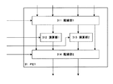
図1において、バスS4に接続されたI/Oデバイス群3は再構成可能なハードウエアを起動する論理回路部起動部7の入力となるn本の割込みソースS1を生成する。論理回路部起動部7では、割込みソースのうち1つを利用して、論理回路部5を起動する論理回路部起動信号S8を生成する。再構成可能なハードウエアである論理回路部5は処理終了後に、論理回路部ACK S9を返してくるので、この信号を新たな割込みソースとして利用し、未処理のn−1本の割込みソースとして合わせて、割込みコントローラ4に入力するn本の割込み要求S5を生成する。
再構成可能ハードウエア(論理回路部)を起動する起動信号S8を生成する割込みソースは任意のものを選択可能であるが、優先度が最高で、最もリアルタイム性を必要とする定周期割り込みとするのが高い効果を得られる。割込みコントローラ4は割り込みS2をCPU1に入力し、CPU1は処理終了後に割込みACK S3を返す。再構成データ制御部6には、論理回路部データS6が保持されたメモリから構成される定義用メモリ部(再構成データ記憶部)61がある。
定義用メモリ部61のメモリはバンク構成となっており、バンクを切り換えるごとに新しい論理回路部データS6が出力される。このバンク切り換えにはインデックスレジスタ62が再構成データ選択レジスタとして利用される。インデックスレジスタ62の設定はCPU1から行なわれ、設定値に変更があった場合に、論理回路部5の再構成を指示する再構成トリガ信号S7が生成される。論理回路部5では再構成トリガ信号S7が生成された時、論理回路部データS6を作用させて、ハードウェアの再構成を行なう。
本発明が特許文献1と異なる部分は、論理回路部起動部7を追加した部分と、論理回路部データS6を常に出力するように変更した点である。
FIG. 1 is a block diagram showing the configuration of the signal processing apparatus according to the first embodiment of the present invention.
In FIG. 1, the I /
The interrupt source that generates the start signal S8 for starting the reconfigurable hardware (logic circuit unit) can be selected arbitrarily, but it has the highest priority and is a periodic interrupt that requires the most real-time capability. High effect can be obtained. The interrupt controller 4 inputs the interrupt S2 to the
The memory of the definition memory unit 61 has a bank configuration, and new logic circuit unit data S6 is output each time the bank is switched. For this bank switching, the
The difference between the present invention and
次に、実施例2について図を参照して説明する。
図2は実施例2の信号処理装置の構成を示すブロック図である。
実施例1と異なる動作の点について説明する。図2において、論理回路部起動部7では、例えば優先度をベースにして、n本の割込みソースS1は調停されて、有る一つの割り込みソースが選択される。この選択された割込みソースを利用して論理回路部起動信号S8を生成する。同時に、どの割込みソースが選択されたかを示す再構成データ選択信号S10を生成する。再構成データ選択信号S10はインデックスレジスタ62に保持されているデータを書き換え、それにより定義用メモリ部61のバンクが変更され、論理回路部5の再構成が割り込みに同期して実行される。
本実施例が前実施例と異なる部分は、実施例1の論理回路部起動部7で再構成データ選択信号S10を生成し、インデックスレジスタ62に作用するように変更した点である。
Next, Example 2 will be described with reference to the drawings.
FIG. 2 is a block diagram illustrating the configuration of the signal processing apparatus according to the second embodiment.
An operation point different from that of the first embodiment will be described. In FIG. 2, in the logic circuit unit activation unit 7, n interrupt sources S1 are arbitrated based on, for example, priority, and one interrupt source is selected. Using this selected interrupt source, the logic circuit unit activation signal S8 is generated. At the same time, a reconfiguration data selection signal S10 indicating which interrupt source has been selected is generated. The reconfiguration data selection signal S10 rewrites the data held in the
This embodiment is different from the previous embodiment in that the reconfiguration data selection signal S10 is generated by the logic circuit section activation unit 7 of the first embodiment and is changed so as to act on the
次に、実施例3について図を参照して説明する。
図3は、実施例3の信号処理装置の構成を示すブロック図である。
実施例1、2と異なる動作の点について説明する。図3において、論理回路部5は、再構成トリガ信号S7をトリガとして、論理回路部データS6を作用させて、ハードウェアの再構成を行なう。
この再構成された状態で、未使用の基本要素が存在している時に、割付制御部51は、どの再構成データ選択信号S10と、基本要素が利用されているかを管理している。ここで、新しい割込みソースが発生した場合、再構成トリガ信号S7が生成され、論理回路部データS6も更新される。割付制御部51は、利用されていなかった部分のみ再構成できるよう、利用している基本要素への再構成トリガ信号S7をマスクして無効とするように制御する。そして、再構成された基本要素と再構成データ選択信号S10をペアで、新たに利用として管理する。
本実施例が、実施例1、2と異なる点は、論理回路部5を実現するための基本要素の割付を制御する、割付制御部51を備えた部分である。
Next, Example 3 will be described with reference to the drawings.
FIG. 3 is a block diagram illustrating the configuration of the signal processing apparatus according to the third embodiment.
Operations different from those in the first and second embodiments will be described. In FIG. 3, the
In this reconfigured state, when there are unused basic elements, the
This embodiment is different from the first and second embodiments in a portion including an
次に、実施例4について図を参照して説明する。
図4は、第4実施例の信号処理装置の構成を示すブロック図である。
実施例1、2、3と異なる動作の点について説明する。図4において、ハードウェアシーケンサ8は、CPUではプログラムとして記述されていた制御シーケンスを、FSM(Finite State Machine:有限状態機械)によりハードウェアで実現したものである。なお、FSMとは、例えば、状態遷移表と呼ばれる各シーケンスをテーブル形式で表したもので、シーケンスの切り換えは、割込み要求S5に同期して行なわれる。
割込み処理の主要な演算処理は論理回路部5で実施しており、バスを操作してI/Oデバイス群3を用いて、上位との通信などの処理を実施する。
本実施例が、実施例1、2、3と異なる点は、CPUとメモリの代わりにハードウェアシーケンサ8を備えた点である。
以上、実施例1〜実施例4が請求項1〜請求項4に該当する第1の発明に関する説明である。
Next, Example 4 will be described with reference to the drawings.
FIG. 4 is a block diagram showing the configuration of the signal processing apparatus according to the fourth embodiment.
Operations different from those of the first, second, and third embodiments will be described. In FIG. 4, the hardware sequencer 8 is a control sequence that is described as a program in the CPU and is realized by hardware using an FSM (Finite State Machine). The FSM is, for example, each sequence called a state transition table expressed in a table format, and switching of the sequence is performed in synchronization with the interrupt request S5.
The main arithmetic processing of the interrupt processing is performed by the
This embodiment is different from the first, second, and third embodiments in that a hardware sequencer 8 is provided instead of the CPU and the memory.
As mentioned above, Example 1- Example 4 is description regarding 1st invention applicable to Claims 1-4.
次に、実施例5について図を参照して説明する。(以下、実施例5〜8は請求項5〜8に該当する第2の発明に関する説明の部分である)。
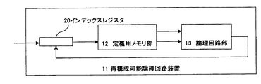
図5は、実施例5の再構成可能論理回路装置のブロック図である。
図5において、再構成可能論理回路装置11は、定義用メモリ12と論理回路部13から構成される。定義用メモリ12は論理回路部13の回路構成が定義されたデータを格納するメモリであり、この定義用メモリ部12の出力を作用させて、論理回路部13の回路構成を変更する。論理回路部13は1つ以上のPE(プロセッサ・エレメント)で構成され、各々のPEは相互接続されている。
さらに、入出力信号もPEと相互接続される。図5では、PE1 31とPE2 32に入力が、PE3 33とPE4 34に出力が接続されている。論理回路部13は、回路構成が定義された後は、専用回路と等価になり、入力信号を利用して演算を行ない、結果を出力信号として再構成可能論理回路装置11の外に転送する。
Next, Example 5 will be described with reference to the drawings. (Hereinafter, Examples 5 to 8 are portions related to the second invention corresponding to
FIG. 5 is a block diagram of the reconfigurable logic circuit device according to the fifth embodiment.
In FIG. 5, the reconfigurable logic circuit device 11 includes a definition memory 12 and a logic circuit unit 13. The definition memory 12 is a memory that stores data in which the circuit configuration of the logic circuit unit 13 is defined. The output of the definition memory unit 12 is operated to change the circuit configuration of the logic circuit unit 13. The logic circuit unit 13 is composed of one or more PEs (processor elements), and each PE is interconnected.
In addition, input / output signals are also interconnected with the PE. In FIG. 5, inputs are connected to PE1 31 and
相互接続された配線と演算回路の再構成はPEの内部で行ない、PE間の接続は固定である。定義用メモリ部12には、このPEと1対1に対応する定義用配列メモリ1 21〜定義用配列メモリ4 24の4つのメモリを備えている。各定義用配列メモリは、PEの内部構成を変更するデータを、配列の形でNセット記憶する。PEを複数に分割し、個々の定義用データをメモリの出力ポート幅と同じか、それ以下に抑える。
これにより、定義用配列メモリへの制御信号を固定することで、メモリ出力を保持でき、特許文献2にある選択制御部のような複雑な回路を排除することができるようになる。また、従来例では揮発性メモリが論理回路部全体の定義用データに相当していたが、本実施例の定義用配列メモリはPEに対する定義用メモリに過ぎず、定義用メモリ部12の出力全体が、論理回路部13の定義用データになる。本例ではPEを4つ、それに対応する定義用配列メモリも4つにしているが、この個数に限定されるものではない。
定義用配列メモリの実装は2次元配列でも構わない。また、定義用配列メモリは不揮発性メモリでも、揮発性メモリでも構わないが、揮発性メモリの場合は電源投入後に定義用配列メモリにデータを書き込む処理が必要となる。
本実施例が特許文献2と異なる部分は、定義用メモリを分割した部分と、論理回路部をPEで構成した部分と、選択制御部を排除した部分である。
Reconfiguration of the interconnected wiring and the arithmetic circuit is performed inside the PE, and the connection between the PEs is fixed. The definition memory unit 12 includes four memories, that is, a
Accordingly, by fixing the control signal to the definition array memory, the memory output can be held, and a complicated circuit such as the selection control unit disclosed in
The implementation of the definition array memory may be a two-dimensional array. The definition array memory may be a non-volatile memory or a volatile memory. In the case of a volatile memory, a process for writing data into the definition array memory after power-on is required.
This embodiment is different from
図6は図5に示す実施例5の構成可能論理回路装置の詳細ブロック図である。 図6は図5に示すPE1の詳細を示したもので、図6を用いて実施例5の動作を説明する。
演算を行う論理回路部13は、入出力データとして14個のレジスタ14と接続されている。PE1 31は3つの入力から1つの演算結果を作成し、PE3 33とPE4 34の入力とする。PE1は演算を実行する演算器としてALU1 18とALU2 19をもつ。ALU1の入力はSW1 15とSW2 16と接続され、レジスタ14と接続されたSW1とSW2は、定義用メモリ部12の定義用配列メモリ1 21のデータを利用して、入力となるレジスタを決定する。
FIG. 6 is a detailed block diagram of the configurable logic circuit device according to the fifth embodiment shown in FIG. FIG. 6 shows details of PE1 shown in FIG. 5. The operation of the
The logic circuit unit 13 that performs the operation is connected to 14 registers 14 as input / output data.
図7は2種類のオペコードを示している。図7(a)は実施例5のオペコードで、ALU1とALU2はオペコードに従って4つの演算を行う。このオペコードも定義用配列メモリの一部である。また、ALU2はALU1の出力とSW3 17の出力を入力として持つ。PE1 31の定義用配列メモリは、SW1、SW2とSW3の12ビットと、ALU1とALU2の4ビットで、合計16ビットになる。
本実施例のように16ビットのポート出力のメモリでは、メモリ自体がデータの保持機能を兼ね備えられるため、メモリ以降にデータの保持機能を持つ必要がなくなる。そのため、4つのPEをもち、各PEが同一の構造である、本実施例では64ビット定義用データが必要となる。
従来例では、64ビットのデータを1個のメモリから出力する必要があり、出力ポートが16ビットや32ビット幅のメモリでは、外部にフリップフロップなどの保持機能が必要となる。本実施例では、アドレスの切り替えで定義用配列メモリのデータを切り替えられるため、クロック単位での切り替えを行えるようになる。さらに、各PEに定義用配列メモリを対応させているため、PE単位でデータの切り替え制御を行うことも可能となる。これによって64ビットにも対応できる。このように図7(a)のオペコードで実施例5と同じ演算を実行する。
なお、図7(b)は実施例5と異なる演算を実行できるオペコードである(これについては後述)。
FIG. 7 shows two types of opcodes. FIG. 7A shows the operation code of the fifth embodiment. ALU1 and ALU2 perform four operations according to the operation code. This opcode is also part of the definition array memory. ALU2 has the output of ALU1 and the output of
In a 16-bit port output memory as in this embodiment, the memory itself has a data holding function, and therefore it is not necessary to have a data holding function after the memory. Therefore, in this embodiment, which has four PEs and each PE has the same structure, 64-bit definition data is required.
In the conventional example, it is necessary to output 64-bit data from one memory, and a memory having a 16-bit or 32-bit width output port requires an external holding function such as a flip-flop. In this embodiment, since the data in the definition array memory can be switched by switching the address, switching can be performed in units of clocks. Furthermore, since the definition array memory is associated with each PE, it is possible to perform data switching control in units of PEs. As a result, 64 bits can be supported. In this way, the same operation as that of the fifth embodiment is executed using the operation code of FIG.
FIG. 7B shows an operation code that can execute an operation different from that in the fifth embodiment (this will be described later).
次に、実施例6について図を参照して説明する。
図8は実施例6の構成を示す再構成可能論理回路装置のブロック図である。
全てのPEの構成は等しいため、PE1 31を代表例として説明する。図8において配線部1 311は複数の入力から、演算部 1 312、配線部2 314への入力を、定義用配列メモリのデータに基づき選択するものである。配線部1 311の入力は、ある時点での演算には利用されない入力もあり、この冗長性により入力の自由度をあげることになる。演算部1 312、演算部2 313の演算も定義用配列メモリのデータに基づき決定される。演算部1、演算部2の出力は配線部2 314に接続され、出力を定義用配列メモリのデータに基づき選択する。この例では演算器は2つであるが、2つに限定されず、多くの演算器を備えることで複雑な演算に対応することができる。これは、配線部も同様である。本実施例が前実施例とは、配線部や演算部で構成されるPEの構成が異なるものである。
Next, Example 6 will be described with reference to the drawings.
FIG. 8 is a block diagram of a reconfigurable logic circuit device showing the configuration of the sixth embodiment.
Since all PEs have the same configuration,
次に、実施例7について図を参照して説明する。
図9は実施例7の構成を示す再構成可能論理回路装置のブロック図である。
図9において、定義用配列メモリ部12(定義用配列メモリ21〜24)の入力の前段にインデックスレジスタ20を配置する。このインデックスレジスタ20は外部のCPU等から読み書き可能とし、インデックスレジスタ20の変更で定義用メモリ部12の各定義用配列メモリ21〜24のデータを変更できる。
本実施例が前実施例と異なる部分は、このインデックスレジスタ20を追加した部分である。
Next, Example 7 will be described with reference to the drawings.
FIG. 9 is a block diagram of a reconfigurable logic circuit device showing the configuration of the seventh embodiment.
In FIG. 9, the index register 20 is arranged before the input of the definition array memory unit 12 (
This embodiment is different from the previous embodiment in that the index register 20 is added.
次に、実施例7の変形例について図を参照して説明する。
図9(b)は、実施例7の変形例の構成を示す再構成可能論理回路装置のブロック図である。
図9(b)において、インデックスレジスタ20を列選択部20aと行選択部20bから構成する。また、定義用配列メモリ部120を2次元配列で構成し、インデックスレジスタ20の列選択部20aと行選択部20bの出力でアドレスを指定する。この2次元配列は、定義用2次元配列メモリ部120(定義用2次元配列メモリ121〜124)である。実施例5と同じく、行選択部20bの内容でPE(図5)の再構成を行なう。さらに、列選択部20aの内容でPEの構成を変更する。例えば、行選択部が1ビットの場合、0と1を値としてとることができる。
0の場合には図6のALU1、ALU2は図7(a)のオペコードを実行するように再構成する。この場合、実施例5と同じ計算をすることが出来る。
次に、1の場合には図6のALU1、ALU2が図7(b)のオペコードを実行するように再構成する。この場合、実施例5と異なる演算を実行できるようになる。これは、列選択部20aの内容で異なるPEを準備しているのと等価であり、アプリケーションにあわせたPEを指定できるようになる。本実施例が実施例7と異なる部分はインデックスレジスタ20と定義用配列メモリ部120とPE(図5)の構成である。
Next, a modification of the seventh embodiment will be described with reference to the drawings.
FIG. 9B is a block diagram of a reconfigurable logic circuit device showing a configuration of a modified example of the seventh embodiment.
In FIG. 9B, the index register 20 includes a column selection unit 20a and a row selection unit 20b. Further, the definition array memory unit 120 is configured in a two-dimensional array, and addresses are designated by the outputs of the column selection unit 20a and the row selection unit 20b of the index register 20. This two-dimensional array is a definition two-dimensional array memory unit 120 (definition two-dimensional array memories 121 to 124). Similar to the fifth embodiment, the PE (FIG. 5) is reconfigured with the contents of the row selection unit 20b. Further, the PE configuration is changed according to the contents of the column selection unit 20a. For example, when the row selection unit is 1 bit, 0 and 1 can be taken as values.
In the case of 0, ALU1 and ALU2 in FIG. 6 are reconfigured to execute the opcode in FIG. In this case, the same calculation as in the fifth embodiment can be performed.
Next, in the case of 1, ALU1 and ALU2 in FIG. 6 are reconfigured to execute the opcode in FIG. 7B. In this case, an operation different from that in the fifth embodiment can be executed. This is equivalent to preparing different PEs according to the contents of the column selection unit 20a, and allows the PEs to be specified according to the application. This embodiment is different from the seventh embodiment in the configuration of the index register 20, the definition array memory unit 120, and the PE (FIG. 5).
次に、実施例8について図を参照して説明する。
図10は実施例8の構成を示す再構成可能論理回路装置のブロック図である。
図10において、定義用配列メモリ1 21〜定義用配列メモリ 4 24の入力の全段にインデックスレジスタ20を配置する。
このインデックスレジスタ20は、論理回路部13の演算結果である出力が接続され、インデックスレジスタ20の値をこの演算結果を用いて変更する。この構成により、論理回路部13で論理回路部の変更条件を演算してインデックスレジスタ20を変更することで、論理回路部13の調整と言える、回路の再構成を実行できるようになる。
さらに、再構成可能論理回路装置11のみで、回路の再構成が実行できるようになる。例えば、外部の環境の違いを論理回路部13で演算し、環境に適合するように論理回路部13の変更を行なえ、環境が変わっても回路を再調整する必要がない装置を提供できるようになる。
また、インデックスレジスタ20は外部のCPU等からも読み書きでき、CPUからの変更も可能とする。本実施例が前実施例と異なる部分は、このインデックスレジスタ20の部分と、インデックスレジスタ20の変更を論理回路部13の演算結果で行なえるようにした点である。
Next, Example 8 will be described with reference to the drawings.
FIG. 10 is a block diagram of a reconfigurable logic circuit device showing the configuration of the eighth embodiment.
In FIG. 10, index registers 20 are arranged in all stages of inputs of the
The index register 20 is connected to an output that is a calculation result of the logic circuit unit 13, and changes the value of the index register 20 using the calculation result. With this configuration, the logic circuit unit 13 calculates a change condition of the logic circuit unit and changes the index register 20, so that circuit reconfiguration that can be said to be adjustment of the logic circuit unit 13 can be executed.
Further, the circuit can be reconfigured only by the reconfigurable logic circuit device 11. For example, it is possible to provide a device in which a difference in the external environment is calculated by the logic circuit unit 13 and the logic circuit unit 13 can be changed so as to suit the environment, and the circuit does not need to be readjusted even if the environment changes. Become.
The index register 20 can be read and written from an external CPU or the like, and can be changed from the CPU. This embodiment is different from the previous embodiment in that the index register 20 and the index register 20 can be changed based on the calculation result of the logic circuit section 13.
次に、実施例9について図を参照して説明する。
以下、実施例9〜実施例12は第3の発明に該当する部分である。
図11は、本発明の実施例9の再構成可能順序回路のブロック図である。
図11において、再構成可能順序回路41はメモリ42と状態制御部301から構成されている。またメモリ42は、状態解釈メモリ101と出力生成メモリ102とメモリ制御部103から構成されている。遷移条件となる入力信号S11は、n1ビット幅の信号であり、このビット幅はある程度の余裕を持たせ、外部に付く回路の増減に対応できるようにする。入力信号S11は状態制御部301に入力される。
状態制御部301は、状態解釈メモリ101の出力である状態解釈信号S15も入力され、この2つの信号によりメモリ制御部103を制御する制御信号S14を生成する。メモリ制御部103は制御信号に従い動作を行い、状態S13を生成する。状態S13は状態解釈メモリ101と出力生成メモリ102のアドレスとして作用し、状態解釈メモリ101は状態解釈信号S15を、出力生成メモリは102は、n2ビットの出力信号S12を生成する。出力信号S12も、外部回路の増減に対応できるように余裕を持ったビット数の信号とする。
Next, Example 9 will be described with reference to the drawings.
Examples 9 to 12 are parts corresponding to the third invention.
FIG. 11 is a block diagram of a reconfigurable sequential circuit according to the ninth embodiment of the present invention.
In FIG. 11, the reconfigurable sequential circuit 41 includes a
The state control unit 301 also receives a state interpretation signal S15 that is an output of the state interpretation memory 101, and generates a control signal S14 for controlling the
この状態遷移に枝分かれがない場合は、
・ 次の状態に遷移する(go)
・ ある遷移条件になるまで状態を保持する(wait)
・ ある状態に遷移する(jump)
という制御を行なえばよい。さらに、枝分かれが必要な時は、
・ ある遷移状態の時は状態Aに、それ以外は状態Bへ遷移する(if〜else〜)を制御に加えることで、任意の状態を取る順序回路とすることができる。さらに、このことは、従来は個別に組み合わせ回路を組んでいた状態遷移の論理を、固定回路とすることができるようになり、本発明の再構成可能順序回路を実現可能とする。
本発明が特許文献3と異なる部分は、状態解釈メモリ101と出力生成メモリ102を備えた部分、および状態解釈メモリ101に状態レジスタの機能を持たせた部分である。
If there is no branching in this state transition,
-Transition to the next state (go)
-Hold the state until a certain transition condition is met (wait)
・ Transition to a certain state (jump)
Control may be performed. Furthermore, when branching is necessary,
A sequential circuit that takes an arbitrary state can be obtained by adding to the control (if-else-) a transition to state A in a certain transition state and transition to state B otherwise. In addition, this makes it possible to use a fixed state circuit as the logic of state transition, which conventionally forms a combinational circuit individually, and makes it possible to realize the reconfigurable sequential circuit of the present invention.
The present invention is different from
図12は図1に示す再構成可能順序回路を利用した回路のブロック図である。図12は、CPU4と2つの外部回路、回路1 2と回路2 3を接続した例であり、入力信号と出力信号はともに4ビットの信号にしている。どちらも1ビットが利用されないが、回路が増えた場合はこの利用されていない信号を利用して対応できる。そのため、物理的な信号線について、入出力信号のビット幅に余裕を持たせておくことで、外部回路の増減への対応を行なえるようになる。論理的な対応は以下説明する。
FIG. 12 is a block diagram of a circuit using the reconfigurable sequential circuit shown in FIG. FIG. 12 shows an example in which the CPU 4 and two external circuits, the circuit 12 and the
図13は、状態解釈メモリ101の内容を示す図である。
図13において、状態S13はアドレスとして利用され、状態S13が示すアドレスの内容が状態解釈信号S15として出力される。
(1)状態が0のとき、
wait S21が、状態解釈メモリの内容であり、入力信号1 S21が真になるまで状態が0を保持し、入力信号1 S21が真になると次の状態である1に遷移する。
(2)同様に、状態が1のとき
wait S22で、入力信号2 S22の状態によって状態遷移が制御される。
(3)状態が2のときは、
wait S23で、入力信号3 S23の状態によって状態遷移が制御される。
状態が3のときは、
jump 0で、このときは無条件に状態が0に遷移する。この状態解釈メモリの内容を変更することで、新たな状態を再構成することができる。さらに、遷移状態に入力信号を利用することが論理的な対応となる。
FIG. 13 is a diagram showing the contents of the state interpretation memory 101.
In FIG. 13, the state S13 is used as an address, and the content of the address indicated by the state S13 is output as the state interpretation signal S15.
(1) When the state is 0,
The wait S21 is the contents of the state interpretation memory. The state holds 0 until the
(2) Similarly, when the state is 1, the state transition is controlled by the state of the
(3) When the state is 2,
In wait S23, the state transition is controlled by the state of the
When the state is 3,
At
次に、図14には出力生成メモリ102の内容を示す。
図14においても状態はアドレスとして利用されているが、出力はこの状態の時の出力信号となる。
(1)状態0の時は、
all 0で、出力信号1〜4 S31〜S34はすべて0の信号が生成される。
状態が1では、
make S31で、出力信号1が1、その他は0の信号になる。
(2)状態2では、
make S32で、出力信号2が1、その他は0の信号になる。
(3)状態3では、
make S33で、出力信号3が1、その他は0の信号になる。
この出力生成メモリの内容を変更することで、出力信号を再構成することができるようになる。状態に出力信号を対応付けできることが論理的な対応となる。さらに、状態解釈メモリ101と出力生成メモリ102は独立しているため、同じ状態で異なる出力信号を生成するなど、再構成の自由度を高めている。
Next, FIG. 14 shows the contents of the output generation memory 102.
Although the state is also used as an address in FIG. 14, the output is an output signal in this state.
(1) When in
In the case of all 0, the
In
In make S31, the
(2) In
In make S32, the
(3) In
In make S33, the
The output signal can be reconfigured by changing the contents of the output generation memory. The logical correspondence is that the output signal can be associated with the state. Furthermore, since the state interpretation memory 101 and the output generation memory 102 are independent, the degree of freedom of reconfiguration is increased by generating different output signals in the same state.
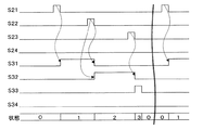
このときの動作波形を図15に示す。
この図は正論理(1のとき真)で記述している。入力信号1 S21が0の時は、状態が0のまま保持されており、出力信号1〜 4 S31〜S34はすべて0である。ある時点で入力信号1が1になった時、状態は1に遷移する。同時に、出力信号1 S31が1になる。この状態では入力信号2 S22を観測している。入力信号2 S22が0の時は現在の状態である1を保持し、1になった時に状態は2に遷移して、同時に出力信号2 S32が1になり、出力信号1を含むその他の信号は0になる。同じく、状態が2では入力信号3 S23を観測し、S23が1になるまで同じ状態を保持し、1になると状態3に遷移する。状態3はすぐに状態0に遷移する。
入力信号1 21はCPU 4の生成した起動信号であり、再構成可能順序回路41はこの起動信号を待っている。起動信号が生成された後に状態は1に遷移して、出力信号1 S31が生成されて回路1 44を起動する。回路1での処理が終了すると、回路1で入力信号2 S22が生成される。
入力信号2は回路1のアクノレッジ信号であり、この信号に同期して状態は2に遷移し、出力信号2 S32が生成される。
出力信号2は回路2 45を起動し、処理終了後にアクノレッジ信号である入力信号3 S23が回路2で生成される。
S23が生成されると状態は3に遷移し、CPUへ回路1と2での処理が終了したことを示す、出力信号3 S33を生成する。この例では、入力信号4 S24と出力信号4 S34は利用されていなかったが、この信号に外部回路を接続し、状態解釈メモリ101と出力生成メモリ102の内容を変更することが、順序回路41の再構成になる。
The operation waveform at this time is shown in FIG.
This figure is described in positive logic (true when 1). When the
The
The
The
When S23 is generated, the state changes to 3, and an
このように、状態解釈メモリ101の出力と入力信号により状態を制御できる構成をしているので、状態解釈メモリ101を変更することで状態遷移を再構成できるのである。
さらに、出力生成メモリ102を変更することで出力の再構成も行うことができる。これはすなわち、順序回路41の再構成を実行できるということである。
Since the state can be controlled by the output and input signal of the state interpretation memory 101 in this way, the state transition can be reconfigured by changing the state interpretation memory 101.
Furthermore, the output can be reconfigured by changing the output generation memory 102. That is, the sequential circuit 41 can be reconfigured.
次に、実施例10について図を参照して説明する。
図16は実施例10の構成を示す図である。
mビット幅の出力生成メモリ102にはエンコードされたデータを記憶する。出力生成メモリ102の後段にデコーダ104を備え、n2ビット幅の出力信号S12を生成させる。このとき、m<n2であり、これにより出力生成メモリの容量を抑えることができるようになる。
本実施例が前実施例と異なる部分は、出力生成メモリ102とデコーダ104を備え、出力生成メモリ102にエンコードされたデータを記憶させるようにした部分である。
このように、出力生成メモリ102の後段にデコーダ104を備える構成をしているので、出力生成メモリ102の容量を抑えることができるので、回路面積を小さくすることができる。
Next, Example 10 will be described with reference to the drawings.
FIG. 16 is a diagram illustrating the configuration of the tenth embodiment.
The m-bit output generation memory 102 stores encoded data. A decoder 104 is provided after the output generation memory 102 to generate an output signal S12 having an n2 bit width. At this time, m <n2, so that the capacity of the output generation memory can be suppressed.
This embodiment is different from the previous embodiment in that the output generation memory 102 and the decoder 104 are provided, and the encoded data is stored in the output generation memory 102.
As described above, since the decoder 104 is provided at the subsequent stage of the output generation memory 102, the capacity of the output generation memory 102 can be suppressed, so that the circuit area can be reduced.
次に、実施例11について図を参照して説明する。
図17は実施例11の構成を示す図である。状態制御部301をルックアップテーブル3011で構成したものである。入力信号S11と状態解釈信号S15を入力として、この入力に対応するように出力信号S12を、ルックアップテーブル3011は生成する。これにより、状態制御部301の論理の変更が可能となり、実施例9で説明した状態制御以外の制御を行うことができるようになるのである。
本実施例が実施例9、10と異なる部分は、状態制御部301をルックアップテーブル3011で構成した部分である。
このように、状態制御部301をルックアップテーブル3011で構成をしているので、任意の状態遷移を行うことできるようになる。
Next, Example 11 will be described with reference to the drawings.
FIG. 17 is a diagram showing the configuration of the eleventh embodiment. The state control unit 301 is configured with a lookup table 3011. The input signal S11 and the state interpretation signal S15 are input, and the look-up table 3011 generates an output signal S12 corresponding to the input. Thereby, the logic of the state control unit 301 can be changed, and control other than the state control described in the ninth embodiment can be performed.
This embodiment is different from the ninth and tenth embodiments in that the state control unit 301 includes a lookup table 3011.
Thus, since the state control unit 301 is configured by the lookup table 3011, any state transition can be performed.
次に、実施例12について図を参照して説明する。
図18は実施例12の構成を示す図である。再構成可能順序回路41は再構成可能データパス50と接続されている。再構成可能順序回路41の出力である出力信号S12は再構成可能データパス50の入力となり、再構成可能データパス50の出力は再構成可能順序回路41の入力信号S11となる。データパス50は演算を行う回路であり、再構成可能順序回路41はデータパス50の動作と再構成の両方を制御する。順序回路41のシーケンスを制御することで、複雑な演算をデータパス50の再構成を行いながら演算できるようになる。
本実施例が前実施例9、10、11と異なる部分は、再構成可能データパス50と再構成可能順序回路41を組み合わせる構成にした部分である。
このように、制御部である順序回路41と演算部分であるデータパス50の両方を再構成可能な構成をしているので、ハードウェアにソフトウェアの柔軟性を持たせることができるので、CPU無しで自律的な動作を可能とすることができる。
Next, Example 12 will be described with reference to the drawings.
FIG. 18 is a diagram showing the configuration of the twelfth embodiment. The reconfigurable sequential circuit 41 is connected to the reconfigurable data path 50. The output signal S12 that is the output of the reconfigurable sequential circuit 41 becomes the input of the reconfigurable data path 50, and the output of the reconfigurable data path 50 becomes the input signal S11 of the reconfigurable sequential circuit 41. The data path 50 is a circuit that performs an operation, and the reconfigurable sequential circuit 41 controls both the operation and reconfiguration of the data path 50. By controlling the sequence of the sequential circuit 41, it is possible to perform complex operations while reconfiguring the data path 50.
This embodiment is different from the previous embodiments 9, 10 and 11 in that the reconfigurable data path 50 and the reconfigurable sequential circuit 41 are combined.
In this way, both the sequential circuit 41 as the control unit and the data path 50 as the calculation part are configured to be reconfigurable, so that the hardware can have software flexibility, so there is no CPU. Can enable autonomous operation.
論理回路部により、ソフトウェア化されたハードウェアを実現できることから、組み込み以外のディジタル信号処理一般に適用できる。
また、環境の変化を計算して求めることによって、環境の変化に回路を適合させることができるので、特に室外でのセンサ処理一般に広く適用できる。
Since the logic circuit unit can realize hardware in software, it can be applied to general digital signal processing other than embedded.
In addition, since the circuit can be adapted to the environmental change by calculating and determining the environmental change, it can be widely applied to sensor processing in general outdoors.
1 CPU
2 メモリ
3 I/Oデバイス群
4 割込みコントローラ
5、13 論理回路部(再構成可能ハードウエア)
51 割付制御部
6 再構成データ制御部
61、12、120 定義用メモリ部(再構成データ記憶部)
62、20 インデックスレジスタ(再構成データ選択レジスタ)
7 論理回路部起動部
8 ハードウェアシーケンサ
11 再構成可能な論理回路装置
14 レジスタ
15 SW1
16 SW2
17 SW3
18 ALU1
19 ALU2
20a 列選択部
20b 行選択部
21〜24、121〜124 定義用配列メモリ
31 PE1
32 PE2
33 PE3
34 PE4
41 再構成可能順序回路
42 メモリ
43 CPU
44 回路1
45 回路2
50 再構成可能データバス
101 状態解釈メモリ
102 出力生成メモリ
103 メモリ制御部
104 デコーダ
301 状態制御部
311 配線部1
312 演算部1
313 演算部2
314 配線部2
3011 ルックアップテーブル
S1 割込みソース
S2 割込み
S3 割込みACK
S4 バス
S5 割込み要求
S6 論理回路部データ
S7 再構成トリガ信号
S8 論理回路部起動信号
S9 論理回路部ACK
S10 再構成データ選択信号
S21 入力信号1
S22 入力信号2
S23 入力信号3
S24 入力信号4
S31 出力信号1
S32 出力信号2
S33 出力信号3
S34 出力信号4
1 CPU
2 Memory 3 I / O device group 4 Interrupt
51 Allocation control unit 6 Reconfiguration data control unit 61, 12, 120 Definition memory unit (reconfiguration data storage unit)
62, 20 Index register (Reconfiguration data selection register)
7 Logic circuit unit start-up unit 8 Hardware sequencer 11 Reconfigurable logic circuit device 14
16 SW2
17 SW3
18 ALU1
19 ALU2
20a column selection unit 20b row selection unit 21-24, 121-124 array memory for
32 PE2
33 PE3
34 PE4
41 reconfigurable
44
45
50 Reconfigurable Data Bus 101 State Interpretation Memory 102
312
313
314
3011 Look-up table S1 Interrupt source S2 Interrupt S3 Interrupt ACK
S4 Bus S5 Interrupt request S6 Logic circuit section data S7 Reconfiguration trigger signal S8 Logic circuit section start signal S9 Logic circuit section ACK
S10 Reconfiguration data selection signal
S24 Input signal 4
S34 Output signal 4
Claims (13)
さらに、再構成ハードウェアデータとして利用するバンクメモリのバンク番号を保持し、バンク番号が変更されると再構成トリガ信号を生成する前記CPUにより設定されるインデックスレジスタと、再構成ハードウェアの構成を決定する構成データを記憶するバンク構成のメモリで、選択されたバンクメモリの出力が再構成ハードウェアデータとして常に前記論理回路部に作用する定義用メモリ部により構成され前記CPUからアクセス可能である再構成データ制御部と、
前記CPUからアクセス可能で、前記論理回路部起動信号により演算処理を開始し、演算処理終了後に論理回路部ACK信号を出力し、再構成ハードウェアデータの内容と再構成トリガ信号に応じてハードウェアの構成を変更する論理回路部と、備えることを特徴とする信号処理装置。 A CPU, a memory, an I / O device group, and an interrupt controller. The n interrupt sources generated by the I / O device group accessible from the CPU are input, and a logic circuit unit start signal is output from an interrupt source. In a signal processing device including a logic circuit unit activation unit that generates and generates an interrupt request from the logic circuit unit ACK signal and other interrupt sources to the interrupt controller,
In addition, the bank number of the bank memory used as reconfigurable hardware data is held, and when the bank number is changed, the index register set by the CPU that generates a reconfiguration trigger signal and the configuration of the reconfigurable hardware A memory having a bank configuration for storing configuration data to be determined. The output of the selected bank memory is configured by a definition memory unit that always acts on the logic circuit unit as reconfigurable hardware data, and can be accessed from the CPU. A configuration data controller;
Accessible from the CPU, starts arithmetic processing in response to the logic circuit section start signal, outputs a logic circuit section ACK signal after the arithmetic processing ends, and performs hardware according to the contents of the reconfigurable hardware data and the reconfiguration trigger signal And a logic circuit unit for changing the configuration of the signal processing apparatus.
回路の増減に対応可能なビット幅を持った入力信号を備え、制御信号から状態を生成するメモリ制御部と、前記状態をアドレスとして利用し状態での動作と入力信号との関連付けを記憶した状態解釈信号を生成する状態解釈メモリと、前記状態をアドレスとして利用し状態に対応する出力信号を記憶して回路の増減に対応可能なビット幅を持つ出力生成メモリから構成されるメモリを備え、前記状態解釈信号と入力信号から前記メモリ制御部の制御信号を生成する状態制御部を備えることを特徴とする再構成可能順序回路。 In a sequential circuit that includes a reconfigurable circuit device and generates an output signal from a state generated by an internal circuit using an input signal as a transition condition,
A memory control unit that has an input signal having a bit width that can correspond to the increase or decrease of the circuit, generates a state from the control signal, and stores the association between the operation in the state and the input signal using the state as an address A state interpretation memory that generates an interpretation signal; and a memory that includes an output generation memory having a bit width that can be used to increase or decrease a circuit by storing an output signal corresponding to the state by using the state as an address, A reconfigurable sequential circuit comprising: a state control unit that generates a control signal for the memory control unit from a state interpretation signal and an input signal.
Priority Applications (1)
| Application Number | Priority Date | Filing Date | Title |
|---|---|---|---|
| JP2005125451A JP2006302132A (en) | 2005-04-22 | 2005-04-22 | Signal processor, reconfigurable logic circuit device and reconfigurable sequential circuit |
Applications Claiming Priority (1)
| Application Number | Priority Date | Filing Date | Title |
|---|---|---|---|
| JP2005125451A JP2006302132A (en) | 2005-04-22 | 2005-04-22 | Signal processor, reconfigurable logic circuit device and reconfigurable sequential circuit |
Publications (1)
| Publication Number | Publication Date |
|---|---|
| JP2006302132A true JP2006302132A (en) | 2006-11-02 |
Family
ID=37470319
Family Applications (1)
| Application Number | Title | Priority Date | Filing Date |
|---|---|---|---|
| JP2005125451A Pending JP2006302132A (en) | 2005-04-22 | 2005-04-22 | Signal processor, reconfigurable logic circuit device and reconfigurable sequential circuit |
Country Status (1)
| Country | Link |
|---|---|
| JP (1) | JP2006302132A (en) |
Cited By (5)
| Publication number | Priority date | Publication date | Assignee | Title |
|---|---|---|---|---|
| JP2013534660A (en) * | 2010-06-10 | 2013-09-05 | マイクロン テクノロジー, インク. | Programmable device, hierarchical parallel machine, and method for providing state information |
| JP2014238861A (en) * | 2011-10-14 | 2014-12-18 | アナログ・デバイシズ・インコーポレーテッド | Dynamically reconfigurable pipelined pre-processor |
| US9146896B2 (en) | 2009-06-25 | 2015-09-29 | Cypress Semiconductor Corporation | Computer system including reconfigurable arithmetic device with network of processor elements |
| JP2017011424A (en) * | 2015-06-19 | 2017-01-12 | ルネサスエレクトロニクス株式会社 | Semiconductor device and control method thereof |
| CN113129961A (en) * | 2021-04-21 | 2021-07-16 | 中国人民解放军战略支援部队信息工程大学 | Configuration circuit for local dynamic reconstruction of cipher logic array |
Citations (10)
| Publication number | Priority date | Publication date | Assignee | Title |
|---|---|---|---|---|
| JPH01147654A (en) * | 1987-12-02 | 1989-06-09 | Mitsubishi Electric Corp | Microcomputer |
| JPH03282602A (en) * | 1990-03-29 | 1991-12-12 | Nec Corp | Sequencer circuit |
| JPH04238189A (en) * | 1991-01-21 | 1992-08-26 | Nippon Telegr & Teleph Corp <Ntt> | Sequence circuit |
| JPH10254696A (en) * | 1997-03-13 | 1998-09-25 | Toshiba Corp | Processor and information processor |
| JP2002169687A (en) * | 2000-12-01 | 2002-06-14 | Nippon Telegr & Teleph Corp <Ntt> | Status transition circuit and its control method |
| JP2002289787A (en) * | 2001-03-28 | 2002-10-04 | Sony Corp | Semiconductor device |
| JP2002297556A (en) * | 2001-03-29 | 2002-10-11 | Fujitsu Ltd | Multiprocessor system, control method and program for multiprocessor, and computer readable recording medium with the program recorded thereon |
| JP2002342068A (en) * | 2001-05-18 | 2002-11-29 | Nippon Telegr & Teleph Corp <Ntt> | State transition circuit and control method therefor |
| JP2006011825A (en) * | 2004-06-25 | 2006-01-12 | Fujitsu Ltd | Reconfigurable arithmetic unit and semiconductor device |
| JP2006018514A (en) * | 2004-06-30 | 2006-01-19 | Fujitsu Ltd | Arithmetic device, control method of arithmetic device, program, and computer-readable recording medium |
-
2005
- 2005-04-22 JP JP2005125451A patent/JP2006302132A/en active Pending
Patent Citations (10)
| Publication number | Priority date | Publication date | Assignee | Title |
|---|---|---|---|---|
| JPH01147654A (en) * | 1987-12-02 | 1989-06-09 | Mitsubishi Electric Corp | Microcomputer |
| JPH03282602A (en) * | 1990-03-29 | 1991-12-12 | Nec Corp | Sequencer circuit |
| JPH04238189A (en) * | 1991-01-21 | 1992-08-26 | Nippon Telegr & Teleph Corp <Ntt> | Sequence circuit |
| JPH10254696A (en) * | 1997-03-13 | 1998-09-25 | Toshiba Corp | Processor and information processor |
| JP2002169687A (en) * | 2000-12-01 | 2002-06-14 | Nippon Telegr & Teleph Corp <Ntt> | Status transition circuit and its control method |
| JP2002289787A (en) * | 2001-03-28 | 2002-10-04 | Sony Corp | Semiconductor device |
| JP2002297556A (en) * | 2001-03-29 | 2002-10-11 | Fujitsu Ltd | Multiprocessor system, control method and program for multiprocessor, and computer readable recording medium with the program recorded thereon |
| JP2002342068A (en) * | 2001-05-18 | 2002-11-29 | Nippon Telegr & Teleph Corp <Ntt> | State transition circuit and control method therefor |
| JP2006011825A (en) * | 2004-06-25 | 2006-01-12 | Fujitsu Ltd | Reconfigurable arithmetic unit and semiconductor device |
| JP2006018514A (en) * | 2004-06-30 | 2006-01-19 | Fujitsu Ltd | Arithmetic device, control method of arithmetic device, program, and computer-readable recording medium |
Cited By (10)
| Publication number | Priority date | Publication date | Assignee | Title |
|---|---|---|---|---|
| US9146896B2 (en) | 2009-06-25 | 2015-09-29 | Cypress Semiconductor Corporation | Computer system including reconfigurable arithmetic device with network of processor elements |
| US10824423B2 (en) | 2009-06-25 | 2020-11-03 | Cypress Semiconductor Corporation | Computer system including reconfigurable arithmetic device with network of processor elements |
| JP2013534660A (en) * | 2010-06-10 | 2013-09-05 | マイクロン テクノロジー, インク. | Programmable device, hierarchical parallel machine, and method for providing state information |
| US10191788B2 (en) | 2010-06-10 | 2019-01-29 | Micron Technology, Inc. | Programmable device, heirarchical parallel machines, and methods for providing state information |
| US11003515B2 (en) | 2010-06-10 | 2021-05-11 | Micron Technology, Inc. | Programmable device, hierarchical parallel machines, and methods for providing state information |
| US11604687B2 (en) | 2010-06-10 | 2023-03-14 | Micron Technology, Inc. | Programmable device, hierarchical parallel machines, and methods for providing state information |
| JP2014238861A (en) * | 2011-10-14 | 2014-12-18 | アナログ・デバイシズ・インコーポレーテッド | Dynamically reconfigurable pipelined pre-processor |
| JP2016167809A (en) * | 2011-10-14 | 2016-09-15 | アナログ・デバイシズ・インコーポレーテッド | Dynamically reconfigurable pipelined pre-processor |
| JP2017011424A (en) * | 2015-06-19 | 2017-01-12 | ルネサスエレクトロニクス株式会社 | Semiconductor device and control method thereof |
| CN113129961A (en) * | 2021-04-21 | 2021-07-16 | 中国人民解放军战略支援部队信息工程大学 | Configuration circuit for local dynamic reconstruction of cipher logic array |
Similar Documents
| Publication | Publication Date | Title |
|---|---|---|
| US10275390B2 (en) | Pipelined configurable processor | |
| JP2011181078A (en) | Programmable circuit and related computing machine, and method | |
| JP4484756B2 (en) | Reconfigurable circuit and processing device | |
| JP2013236380A (en) | Programmable circuit, related computing machine, and method | |
| JP2008537268A (en) | An array of data processing elements with variable precision interconnection | |
| JP2006018453A (en) | Semiconductor device | |
| US7352205B2 (en) | Reconfigurable switching device parallel calculation of any particular algorithms | |
| JP2006302132A (en) | Signal processor, reconfigurable logic circuit device and reconfigurable sequential circuit | |
| JP2007272671A (en) | Motion composition device, debugging device, write device and circuit design support system and method | |
| JP4451733B2 (en) | Semiconductor device | |
| US7509479B2 (en) | Reconfigurable global cellular automaton with RAM blocks coupled to input and output feedback crossbar switches receiving clock counter value from sequence control unit | |
| US8607029B2 (en) | Dynamic reconfigurable circuit with a plurality of processing elements, data network, configuration memory, and immediate value network | |
| JP4468452B2 (en) | Computer device with a reconfigurable architecture to incorporate global cellular automata | |
| JP2010206513A (en) | Semiconductor device | |
| JP2006018411A (en) | Processor | |
| JP2008293226A (en) | Semiconductor device | |
| JP4787711B2 (en) | Data processing apparatus and method, computer program, information storage medium, and data processing system | |
| JP6553694B2 (en) | Processor element, programmable device and control method of processor element | |
| JP6046319B1 (en) | Serial configuration of reconfigurable instruction cell array | |
| JPH053015B2 (en) | ||
| JP2008165537A (en) | Dynamic reconfigurable processor and reconfiguration instructing method | |
| JP3989397B2 (en) | Integrated circuit device and data setting device for the device | |
| JP2008219728A (en) | Reconstructible arithmetic processing circuit | |
| JP2007257216A (en) | Parallel processor for dynamically switching circuit configuration | |
| JP5701930B2 (en) | Semiconductor device |
Legal Events
| Date | Code | Title | Description |
|---|---|---|---|
| RD04 | Notification of resignation of power of attorney |
Free format text: JAPANESE INTERMEDIATE CODE: A7424 Effective date: 20071127 |
|
| A621 | Written request for application examination |
Free format text: JAPANESE INTERMEDIATE CODE: A621 Effective date: 20080314 |
|
| A131 | Notification of reasons for refusal |
Free format text: JAPANESE INTERMEDIATE CODE: A131 Effective date: 20100615 |
|
| A521 | Written amendment |
Free format text: JAPANESE INTERMEDIATE CODE: A523 Effective date: 20100723 |
|
| A131 | Notification of reasons for refusal |
Free format text: JAPANESE INTERMEDIATE CODE: A131 Effective date: 20110405 |
|
| A02 | Decision of refusal |
Free format text: JAPANESE INTERMEDIATE CODE: A02 Effective date: 20110802 |