JP2006294703A - Semiconductor device and its manufacturing method, and liquid crystal display - Google Patents
Semiconductor device and its manufacturing method, and liquid crystal display Download PDFInfo
- Publication number
- JP2006294703A JP2006294703A JP2005110250A JP2005110250A JP2006294703A JP 2006294703 A JP2006294703 A JP 2006294703A JP 2005110250 A JP2005110250 A JP 2005110250A JP 2005110250 A JP2005110250 A JP 2005110250A JP 2006294703 A JP2006294703 A JP 2006294703A
- Authority
- JP
- Japan
- Prior art keywords
- insulating film
- substrate
- gate electrode
- film
- semiconductor
- Prior art date
- Legal status (The legal status is an assumption and is not a legal conclusion. Google has not performed a legal analysis and makes no representation as to the accuracy of the status listed.)
- Granted
Links
Images


Landscapes
- Thin Film Transistor (AREA)
- Electrodes Of Semiconductors (AREA)
Abstract
Description
本発明は、半導体装置の製造方法及び半導体装置並びに液晶表示装置に関するものである。 The present invention relates to a method for manufacturing a semiconductor device, a semiconductor device, and a liquid crystal display device.
従来より、絶縁層の表面に単結晶のシリコン層が形成されたシリコン基板であるSOI(Silicon On Insulator)基板が知られている。SOI基板にトランジスタ等のデバイスを形成することにより、寄生容量を低減すると共に絶縁抵抗を高くすることができる。すなわち、デバイスの高集積化や高性能化を図ることができる。上記絶縁層は、例えばシリコン酸化膜(SiO2)により形成されている。 2. Description of the Related Art Conventionally, an SOI (Silicon On Insulator) substrate is known which is a silicon substrate in which a single crystal silicon layer is formed on the surface of an insulating layer. By forming a device such as a transistor on an SOI substrate, parasitic capacitance can be reduced and insulation resistance can be increased. That is, higher integration and higher performance of the device can be achieved. The insulating layer is formed of, for example, a silicon oxide film (SiO 2 ).
上記SOI基板は、デバイスの動作速度を高めると共に寄生容量をさらに低減するために、単結晶シリコン層の膜厚を薄く形成することが望ましい。そこで、従来より、シリコン基板をガラス基板等の他の基板に貼り合わせた後に、シリコン基板の一部を分離除去することにより、SOI基板を作製する方法が知られている(例えば、非特許文献1参照)。 In order to increase the operation speed of the device and further reduce the parasitic capacitance, the SOI substrate is desirably formed with a thin single crystal silicon layer. Therefore, conventionally, a method of manufacturing an SOI substrate by separating and removing a part of the silicon substrate after bonding the silicon substrate to another substrate such as a glass substrate is known (for example, non-patent document). 1).
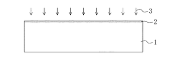
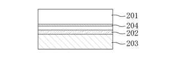
ここで、上記貼り合わせによるSOI基板の作製方法について、図28〜図31を参照して説明する。なお、SOI層の薄膜化の方法は、機械研磨や化学ポリッシングやポーラスシリコンを利用した手法など種々あるが、ここでは、水素注入による方法について示す。まず、図28に示すように、第1の基板であるシリコン基板201の表面を酸化処理することにより、絶縁層である酸化シリコン(SiO2)層202を形成する。次に、図29に示すように、酸化シリコン(SiO2)層202を介してシリコン基板201中に、剥離用物質である水素をイオン注入する。このことにより、シリコン基板201の所定の深さ位置に剥離層である水素注入層204を形成する。続いて、RCA洗浄等の基板表面洗浄処理を行った後、図30に示すように、上記酸化シリコン層202の表面に第2の基板である例えばシリコン基板203を貼り付ける。その後、熱処理を行うことにより、水素イオン注入深さ部分にマイクロクラックが形成されるため、図31に示すように、シリコン基板201の一部を上記水素注入層204に沿って分離する。こうして、シリコン基板201を薄膜化してシリコン層201を形成する。なお、分離後、必要に応じて研磨、エッチング等の種々の手法によって所望の膜厚に薄膜化し、また、熱処理等により水素注入によって生成される結晶欠陥修復やシリコン表面の平滑化等を行う。
Here, a method for manufacturing an SOI substrate by the above bonding will be described with reference to FIGS. Note that there are various methods for thinning the SOI layer, such as mechanical polishing, chemical polishing, and methods using porous silicon. Here, a method using hydrogen injection is described. First, as shown in FIG. 28, the surface of a
以上のようにして、シリコン基板(第2の基板)203の表面にSiO2層(絶縁層)202が形成されると共に、SiO2層202の表面にシリコン層201が薄く形成されたSOI基板が作製される。
本発明者らは、MOSトランジスタ等の半導体素子を有する半導体基板に対し、水素注入層を形成して半導体基板の一部を分離することにより、半導体素子を他の基板上に薄膜化して製造できることを見出した。このことにより、上記他の基板を透明基板とすることによって、半導体層が薄膜化された半導体装置を、液晶表示装置に適用することが可能となる。 The present inventors can manufacture a semiconductor element thinned on another substrate by forming a hydrogen injection layer and separating a part of the semiconductor substrate from a semiconductor substrate having a semiconductor element such as a MOS transistor. I found. Thus, by using the other substrate as a transparent substrate, a semiconductor device with a thin semiconductor layer can be applied to a liquid crystal display device.
ところで、上記他の基板に半導体素子であるトランジスタを薄膜化して形成した場合、そのゲート電極に対向して形成されるチャネル領域は、シリコン層が50〜100nm以下程度に薄いことが望ましい。なぜなら、チャネル領域のシリコン層を薄く形成することにより完全空乏型のSOI動作が可能となって、Bulkシリコントランジスタに比べて優れたサブスレッシュホールド特性が得られるためである。その結果、トランジスタの低電圧化、高速化、及び低消費電力化を図ることができる。特に、スケーリング則によりゲート長が短くなるに連れてチャネル領域の不純物元素濃度を高くする必要があるため、シリコン層は薄くすることが好ましい。この点で、本発明者らが見出した上記半導体層が薄膜化された半導体装置は好適である。 By the way, when a transistor, which is a semiconductor element, is formed on the other substrate as a thin film, the channel region formed to face the gate electrode preferably has a silicon layer as thin as about 50 to 100 nm or less. This is because by forming a thin silicon layer in the channel region, a fully depleted SOI operation is possible, and an excellent subthreshold characteristic can be obtained as compared with a bulk silicon transistor. As a result, the transistor can be reduced in voltage, increased in speed, and reduced in power consumption. In particular, since the impurity element concentration in the channel region needs to be increased as the gate length becomes shorter due to the scaling law, the silicon layer is preferably thin. In this respect, the semiconductor device in which the semiconductor layer found by the present inventors is thinned is preferable.
しかしながら、トランジスタのソース領域及びドレイン領域では、シリコン層を薄くすると、それに逆比例してシート抵抗が大きくなるため、寄生抵抗が増大し、ソース領域及びドレイン領域におけるコンタクト抵抗も増大してしまう。すなわち、シリコン層を薄くし過ぎると、トランジスタの性能を低下させる要因となる。このように、半導体層を薄膜化することは、ゲート電極に対向する領域においては好ましいが、その他の領域においては問題になってしまう。 However, in the source region and the drain region of the transistor, when the silicon layer is thinned, the sheet resistance increases in inverse proportion thereto, so that the parasitic resistance increases and the contact resistance in the source region and the drain region also increases. That is, if the silicon layer is made too thin, it becomes a factor that degrades the performance of the transistor. Thus, it is preferable to reduce the thickness of the semiconductor layer in a region facing the gate electrode, but it becomes a problem in other regions.
本発明は、斯かる諸点に鑑みてなされたものであり、その目的とするところは、半導体基板に対し、その一部を剥離層に沿って確実に剥離すると共に、ゲート電極に対向する領域では比較的薄くする一方、その他の領域では比較的厚く形成することにより、半導体装置の特性を向上させることにある。 The present invention has been made in view of such various points. The object of the present invention is to reliably peel a part of a semiconductor substrate along a peeling layer and to face a gate electrode. It is intended to improve the characteristics of the semiconductor device by forming it relatively thin while forming it relatively thick in other regions.
すなわち、半導体装置の特性を向上させるためには、チャネル領域では半導体層の厚みを小さくする一方、ソース領域及びドレイン領域では半導体層の厚みを比較的大きくすることが有効であると考えられる。したがって、本発明者らは、半導体層における剥離層の深さを、チャネル領域において比較的浅くする一方、ソース領域及びドレイン領域において比較的深くすることを考えた。 That is, in order to improve the characteristics of the semiconductor device, it is considered effective to reduce the thickness of the semiconductor layer in the channel region and relatively increase the thickness of the semiconductor layer in the source region and the drain region. Therefore, the present inventors have considered that the depth of the separation layer in the semiconductor layer is relatively shallow in the channel region while being relatively deep in the source region and the drain region.
ところが、本発明者らの実験により、剥離用物質の半導体層への注入深さの分布(つまり剥離層の深さ)が、その最大傾斜角度が70°程度以上に急峻に変化した場合には、半導体層を剥離層に沿って分離させようとすると、その急峻な変化位置の近傍で予期せぬ分離が起こってしまい、剥離層に沿って上手く分離できないことを確認している。 However, according to the experiments conducted by the present inventors, when the distribution of the implantation depth of the peeling material into the semiconductor layer (that is, the depth of the peeling layer) changes abruptly such that the maximum inclination angle is about 70 ° or more. It has been confirmed that when the semiconductor layer is separated along the peeling layer, unexpected separation occurs in the vicinity of the steep change position, and the semiconductor layer cannot be separated well along the peeling layer.
そこで、上記の目的を達成するために、この発明では、半導体基板の表面とゲート電極の表面とに対応して形成される表面段差形状をなだらかな表面段差形状に補償するための絶縁膜を設けるようにした。 Therefore, in order to achieve the above object, in the present invention, an insulating film is provided for compensating the surface step shape formed corresponding to the surface of the semiconductor substrate and the surface of the gate electrode to a smooth surface step shape. I did it.
具体的に、本発明に係る半導体装置の製造方法は、半導体基板にゲート電極を形成するゲート電極形成工程と、上記半導体基板の表面とゲート電極の表面とに対応して形成される表面段差形状をなだらかな表面段差形状に補償するための絶縁膜を、上記ゲート電極及び上記半導体基板を覆うように形成する絶縁膜形成工程と、上記半導体基板に対し、上記絶縁膜を介して剥離用物質をイオン注入することにより、剥離層を形成する剥離層形成工程と、上記半導体基板の一部を上記剥離層に沿って分離する分離工程とを備えている。 Specifically, the method of manufacturing a semiconductor device according to the present invention includes a gate electrode forming step of forming a gate electrode on a semiconductor substrate, and a surface step shape formed corresponding to the surface of the semiconductor substrate and the surface of the gate electrode. An insulating film forming step for covering the gate electrode and the semiconductor substrate with an insulating film for compensating for a smooth surface step shape, and a peeling substance is formed on the semiconductor substrate via the insulating film. A separation layer forming step for forming a separation layer by ion implantation and a separation step for separating a part of the semiconductor substrate along the separation layer are provided.
上記絶縁膜は、上記半導体基板の表面に対する最大傾斜角度θが、0°<θ≦50°の範囲に規定されていることが好ましい。 The insulating film preferably has a maximum inclination angle θ with respect to the surface of the semiconductor substrate in a range of 0 ° <θ ≦ 50 °.
上記絶縁膜形成工程の後に行われ、上記絶縁膜における上記ゲート電極を覆っている部分を薄膜化する薄膜化工程を含むようにしてもよい。 A step of reducing the thickness of the portion of the insulating film covering the gate electrode that is performed after the insulating film forming step may be included.
上記半導体基板及び上記絶縁膜を覆う平坦化膜を形成する平坦化膜形成工程と、上記平坦化膜に基板を接合する接合工程とを備え、上記接合工程は、上記分離工程よりも前に行われることが好ましい。 A planarization film forming step for forming a planarization film covering the semiconductor substrate and the insulating film; and a bonding step for bonding the substrate to the planarization film. The bonding step is performed before the separation step. Are preferred.
上記基板は透明基板であってもよい。 The substrate may be a transparent substrate.
上記半導体基板はシリコン基板であることが好ましい。 The semiconductor substrate is preferably a silicon substrate.
上記剥離用物質は、水素及び不活性ガス元素の少なくとも一方であることが好ましい。 The stripping material is preferably at least one of hydrogen and an inert gas element.
上記ゲート電極は、MOSトランジスタを構成するようにしてもよい。 The gate electrode may constitute a MOS transistor.
上記絶縁膜は、BPSG(Borophosphosilicate glass)膜であることが好ましい。 The insulating film is preferably a BPSG (Borophosphosilicate glass) film.
上記BPSG膜は、上記絶縁膜形成工程において900℃以上の温度で熱処理されるようにしてもよい。 The BPSG film may be heat-treated at a temperature of 900 ° C. or higher in the insulating film forming step.
上記接合工程よりも前に行われ、上記基板に能動素子及び受動素子の少なくとも一方を予め形成する素子形成工程と、上記ゲート電極が形成された半導体基板に活性領域を形成する活性領域形成工程と、上記接合工程よりも後に行われ、上記活性領域と、上記基板に形成されている能動素子及び受動素子の少なくとも一方とを電気的に接続する接続工程とを備えていることが好ましい。 An element forming step for forming at least one of an active element and a passive element on the substrate in advance, and an active region forming step for forming an active region on the semiconductor substrate on which the gate electrode is formed; Preferably, the method includes a connection step that is performed after the bonding step and electrically connects the active region and at least one of the active element and the passive element formed on the substrate.
また、本発明に係る半導体装置は、半導体層と、上記半導体層に形成されたゲート電極と、上記ゲート電極及び上記半導体層を覆うように形成され、上記ゲート電極の表面と半導体層の表面とに対応して形成される表面段差形状をなだらかな表面段差形状に補償するための絶縁膜とを備え、上記半導体層は、上記絶縁膜の表面段差形状に沿って形成された表面を有している。 Further, a semiconductor device according to the present invention is formed so as to cover a semiconductor layer, a gate electrode formed in the semiconductor layer, the gate electrode and the semiconductor layer, and a surface of the gate electrode and a surface of the semiconductor layer. An insulating film for compensating the surface step shape formed to correspond to a smooth surface step shape, and the semiconductor layer has a surface formed along the surface step shape of the insulating film. Yes.
上記半導体層の一部は、剥離物質がイオン注入されることにより形成された剥離層に沿って分離されていることが好ましい。 Part of the semiconductor layer is preferably separated along a release layer formed by ion implantation of a release substance.
上記絶縁膜は、上記半導体層の表面に対する最大傾斜角度θが、0°<θ≦50°の範囲に規定されていることが好ましい。 The insulating film preferably has a maximum inclination angle θ with respect to the surface of the semiconductor layer in a range of 0 ° <θ ≦ 50 °.
上記絶縁膜は、上記ゲート電極を覆っている部分が薄膜化して形成されていてもよい。 The insulating film may be formed by thinning a portion covering the gate electrode.
上記半導体層及び上記絶縁膜を覆う平坦化膜と、上記平坦化膜の表面に接合された基板とを備えていることが好ましい。 It is preferable to include a planarization film that covers the semiconductor layer and the insulating film, and a substrate that is bonded to the surface of the planarization film.
上記基板は透明基板であってもよい。 The substrate may be a transparent substrate.
上記半導体層はシリコン層であることが好ましい。 The semiconductor layer is preferably a silicon layer.
上記剥離用物質は、水素及び不活性ガス元素の少なくとも一方であることが好ましい。 The stripping material is preferably at least one of hydrogen and an inert gas element.
上記ゲート電極は、MOSトランジスタを構成しているようにしてもよい。 The gate electrode may constitute a MOS transistor.
上記絶縁膜は、BPSG(Borophosphosilicate glass)膜であることが好ましい。 The insulating film is preferably a BPSG (Borophosphosilicate glass) film.
上記BPSG膜は、900℃以上の温度で熱処理されていてもよい。 The BPSG film may be heat-treated at a temperature of 900 ° C. or higher.
上記絶縁膜は、SOG(Spin On Glass)膜であってもよい。 The insulating film may be a SOG (Spin On Glass) film.
上記絶縁膜形成工程の前に行われ、上記ゲート電極に重ならないようにダミーパターンを形成するダミーパターン形成工程を備え、上記絶縁膜形成工程では、上記ダミーパターン、上記ゲート電極及び上記半導体基板を覆うように、上記絶縁膜を形成するようにしてもよい。 A dummy pattern forming step is performed before the insulating film forming step to form a dummy pattern so as not to overlap the gate electrode. In the insulating film forming step, the dummy pattern, the gate electrode, and the semiconductor substrate are formed. The insulating film may be formed so as to cover it.
上記半導体層には、活性領域が形成され、上記基板には、能動素子及び受動素子の少なくとも一方が、上記活性領域に電気的に接続して形成されていることが好ましい。 An active region is preferably formed in the semiconductor layer, and at least one of an active element and a passive element is preferably formed on the substrate in electrical connection with the active region.
また、本発明に係る液晶表示装置は、複数の薄膜トランジスタが形成されたアクティブマトリクス基板を有する液晶表示装置であって、上記薄膜トランジスタは、半導体層と、上記半導体層に形成されたゲート電極と、上記ゲート電極及び上記半導体層を覆うように形成され、上記ゲート電極の表面と半導体層の表面とに対応して形成される表面段差形状をなだらかな表面段差形状に補償するための絶縁膜とを備え、上記半導体層は、上記絶縁膜の表面段差形状に沿って形成された表面を有している。 The liquid crystal display device according to the present invention is a liquid crystal display device having an active matrix substrate on which a plurality of thin film transistors are formed. The thin film transistor includes a semiconductor layer, a gate electrode formed in the semiconductor layer, and An insulating film formed so as to cover the gate electrode and the semiconductor layer and for compensating the surface step shape formed corresponding to the surface of the gate electrode and the surface of the semiconductor layer to a gentle surface step shape; The semiconductor layer has a surface formed along the surface step shape of the insulating film.
−作用−
次に、本発明の作用について説明する。
-Action-
Next, the operation of the present invention will be described.
本発明により半導体装置を製造する場合には、まずゲート電極形成工程において、半導体基板にゲート電極を形成する。その結果、半導体基板には、該半導体基板の表面とゲート電極の表面とに対応して表面段差形状が形成される。 When manufacturing a semiconductor device according to the present invention, first, a gate electrode is formed on a semiconductor substrate in a gate electrode formation step. As a result, a surface step shape is formed on the semiconductor substrate corresponding to the surface of the semiconductor substrate and the surface of the gate electrode.
続いて、絶縁膜形成工程において、上記ゲート電極及び半導体基板を覆うように絶縁膜を形成する。このことにより、上記半導体基板の表面とゲート電極の表面とに対応して形成される表面段差形状は、急峻な表面段差形状であっても、上記絶縁膜に覆われることにより、上記表面段差形状はなだらかな表面段差形状に補償される。上記絶縁膜には、例えばBPSG膜が好適である。 Subsequently, in the insulating film forming step, an insulating film is formed so as to cover the gate electrode and the semiconductor substrate. Accordingly, even if the surface step shape formed corresponding to the surface of the semiconductor substrate and the surface of the gate electrode is a steep surface step shape, the surface step shape is covered by the insulating film. The smooth surface step shape is compensated. For example, a BPSG film is suitable for the insulating film.
尚、上記絶縁膜形成工程の前に、ダミーパターン形成工程を行い、ゲート電極に重ならないようにダミーパターンを形成しておくことで、絶縁膜の表面段差形状のなだらかさを調節することが可能となる。 It is possible to adjust the smoothness of the surface step shape of the insulating film by performing a dummy pattern forming process before the insulating film forming process and forming a dummy pattern so as not to overlap the gate electrode. It becomes.
次に、剥離層形成工程において、上記半導体基板に対し、上記絶縁膜を介して剥離用物質をイオン注入する。その結果、半導体基板には剥離用物質が注入された剥離層が形成される。このとき、剥離用物質は、上記絶縁膜の表面に沿った深さ位置に注入されるため、剥離層の深さ位置を、上記なだらかな表面段差形状である絶縁膜表面に沿ってなだらかに変化させることができる。言い換えれば、剥離用物質をイオン注入する基板表面が上記絶縁膜によってなだらかな表面段差形状に補償されるため、剥離層の深さ位置を急峻に変化させないようにすることが可能となる。 Next, in the peeling layer forming step, a peeling material is ion-implanted into the semiconductor substrate through the insulating film. As a result, a peeling layer into which a peeling material is injected is formed on the semiconductor substrate. At this time, since the release material is injected into the depth position along the surface of the insulating film, the depth position of the release layer changes gently along the surface of the insulating film having the gentle surface step shape. Can be made. In other words, the surface of the substrate into which the release material is ion-implanted is compensated for a smooth surface step shape by the insulating film, so that the depth position of the release layer can be prevented from changing sharply.
その後、分離工程において、上記半導体基板の一部は、深さ位置がなだらかに変化する上記剥離層に沿って分離される。その結果、残った半導体基板の厚みは、自己整合的に、ゲート電極が設けられている領域において比較的薄く形成される一方、ゲート電極が設けられていない領域において比較的厚く形成されることとなる。 Thereafter, in the separation step, a part of the semiconductor substrate is separated along the release layer whose depth position changes gently. As a result, the remaining semiconductor substrate is formed to be relatively thin in the region where the gate electrode is provided, while being relatively thick in the region where the gate electrode is not provided, in a self-aligned manner. Become.
上記絶縁膜における表面段差形状は、仮に、その最大傾斜角度θが50°よりも大きくなると、剥離層が急峻に変化することとなるため、分離工程において、半導体基板の一部が予期せぬ位置で分離してしまい、半導体基板の一部を剥離層に沿って分離させることができない。一方、最大傾斜角度θが0°では、絶縁膜の表面をなだらかな表面段差形状に形成することができない。したがって、最大傾斜角度θが0°<θ≦50°に規定することによって、なだらかな表面段差形状の剥離層に沿って、半導体基板の一部を剥離させることが可能となる。 If the maximum inclination angle θ is larger than 50 °, the surface step shape in the insulating film is abruptly changed in the release layer. And part of the semiconductor substrate cannot be separated along the release layer. On the other hand, when the maximum inclination angle θ is 0 °, the surface of the insulating film cannot be formed into a gentle surface step shape. Therefore, by setting the maximum inclination angle θ to 0 ° <θ ≦ 50 °, it becomes possible to peel a part of the semiconductor substrate along the release layer having a gentle surface step shape.
特に、絶縁膜形成工程の後に、薄膜化工程を行い、絶縁膜におけるゲート電極を覆っている部分を薄膜化することにより、半導体基板におけるゲート電極の下方の領域において、剥離層を深い位置に形成することが可能となる。 In particular, a thinning process is performed after the insulating film forming process, and a part of the insulating film covering the gate electrode is thinned to form a peeling layer at a deep position in the region below the gate electrode in the semiconductor substrate. It becomes possible to do.
また、平坦化膜形成工程において半導体基板及び絶縁膜を平坦化膜で覆うと共に、接合工程において平坦化膜の表面に基板を接合し、その後に、上記分離工程を行うことによって、一部が剥離層に沿って分離されることで薄型化されると共にゲート電極等が形成された半導体基板の残りの部分を上記基板へ移すことが可能となる。 In addition, the semiconductor substrate and the insulating film are covered with a planarization film in the planarization film forming process, and the substrate is bonded to the surface of the planarization film in the bonding process, and then the separation process is performed, so that a part is peeled off By separating along the layers, the remaining portion of the semiconductor substrate on which the gate electrode and the like are formed can be transferred to the substrate.
また、素子形成工程において、上記基板に能動素子及び受動素子の少なくとも一方を予め形成する一方、活性領域形成工程において半導体基板に活性領域を形成する。その後、接合工程の後に、接続工程を行い、上記活性領域と、上記能動素子及び受動素子の少なくとも一方とを電気的に接続することが可能である。 In the element forming step, at least one of an active element and a passive element is formed in advance on the substrate, and in the active region forming step, an active region is formed on the semiconductor substrate. Then, after the joining step, a connection step can be performed to electrically connect the active region and at least one of the active element and the passive element.
本発明によれば、半導体基板の表面とゲート電極の表面とに対応して形成される表面段差形状が急峻であっても、これら半導体基板及びゲート電極を絶縁膜によって覆うことにより、なだらかな表面段差形状に補償することができる。そのことにより、剥離用物質は、半導体基板である半導体層に対し、なだらかな絶縁膜の表面形状に沿った深さ位置に注入されるため、剥離層の深さ位置をなだらかに変化させることができ、剥離層の深さ位置を急峻に変化させないようにすることができる。そのため、半導体基板の一部を、剥離層に沿って確実に剥離することができる。 According to the present invention, even if the surface step shape formed corresponding to the surface of the semiconductor substrate and the surface of the gate electrode is steep, by covering the semiconductor substrate and the gate electrode with the insulating film, the smooth surface The step shape can be compensated. As a result, the release substance is injected into the semiconductor layer which is a semiconductor substrate at a depth position along the surface shape of the gentle insulating film, so that the depth position of the release layer can be changed gently. In addition, the depth position of the release layer can be prevented from changing abruptly. Therefore, a part of the semiconductor substrate can be reliably peeled along the peeling layer.
また、このとき、剥離層の深さ位置を、ゲート電極に対向する領域では浅く形成すると共に、その他の領域では深く形成することができるため、半導体基板を、ゲート電極に対向する領域では比較的薄くする一方、その他の領域では比較的厚く形成することできる。その結果、半導体装置の特性を向上させることができる。 At this time, since the depth position of the peeling layer can be formed shallow in the region facing the gate electrode and deep in other regions, the semiconductor substrate can be relatively formed in the region facing the gate electrode. While it can be made thinner, it can be made relatively thick in other areas. As a result, the characteristics of the semiconductor device can be improved.
以下、本発明の実施形態を図面に基づいて詳細に説明する。尚、本発明は、以下の実施形態に限定されるものではない。 Hereinafter, embodiments of the present invention will be described in detail with reference to the drawings. The present invention is not limited to the following embodiment.
《発明の実施形態1》
図1〜図16及び図27は、本発明の実施形態1を示している。図1は、本発明に係る半導体装置の実施形態である薄膜トランジスタ(以降、TFTと略称する)50を示す断面図である。また、図2〜図16は、TFT50の製造方法を説明する断面図であり、図27は、本発明の実施形態である液晶表示装置Sの要部を概略的に示す断面図である。
1 to 16 and FIG. 27
液晶表示装置Sは、図27に示すように、アクティブマトリクス基板42と、このアクティブマトリクス基板42に対向して設けられた対向基板43と、これらの基板42,43の間に形成された液晶層44とを備えている。
As shown in FIG. 27, the liquid crystal display device S includes an
上記アクティブマトリクス基板42には、複数の画素(図示省略)が設けられ、図1に示すような複数のTFT50が各画素毎に形成されている。また、アクティブマトリクス基板42は、液晶層44側の表面に配向膜45が設けられると共に、液晶層44とは反対側の表面に偏光板46が積層されている。また、アクティブマトリクス基板42には、各TFT50を駆動制御するためのICドライバ(図示省略)が設けられている。
The
上記対向基板43には、図示を省略するが、カラーフィルタやITOからなる共通電極等が形成されている。また、対向基板43は、液晶層44側の表面に配向膜47が設けられると共に、液晶層44とは反対側の表面に偏光板48が積層されている。また、上記液晶層44は、アクティブマトリクス基板42と対向基板43との間に介在されたスペーサ49によって封止されている。こうして、液晶表示装置Sは、TFT50により液晶層44における液晶分子の配向状態を制御して、所望の表示を行うようになっている。
Although not shown, the
尚、本実施形態では、各画素における表示を制御するTFT50を例に挙げて、本発明に係る半導体装置を説明するが、本発明は、例えば上記ICドライバに用いられるトランジスタとしても適用することができる。また、1つのNMOSトランジスタであるTFT50について説明し、PMOSトランジスタについては説明しないが、イオン注入時の不純物の導電型を適宜変更することにより、NMOSトランジスタと同様に形成することができる。また、半導体装置は複数のNMOSトランジスタやPMOSトランジスタが同一の半導体基板上に作り込まれた構造となっている。また、各トランジスタは、LOCOS法やトレンチアイソレーション等により適宜素子分離されている。
In the present embodiment, the semiconductor device according to the present invention will be described by taking the
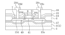
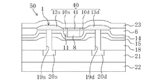
上記TFT50は、図1に示ように、透明基板であるガラス基板22に形成され、活性領域40を含む半導体層1と、ゲート電極8とを備えている。
As shown in FIG. 1, the
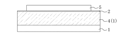
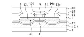
ガラス基板22には、第1の平坦化膜である絶縁膜21と、第2の平坦化膜である層間絶縁膜18と、絶縁膜であるBPSG(Borophosphosilicate glass:ボロンリンガラス)膜15と、絶縁膜14とがこの順に積層されている。言い換えれば、絶縁膜21及び層間絶縁膜18は、半導体層1及びBPSG膜15を覆うように設けられている。そして、ガラス基板22は、絶縁膜21の表面に接合されている。また、BPSG膜は、900℃以上の温度で熱処理されている。
The
層間絶縁膜18とBPSG膜15との界面は、なだらかな表面段差形状に形成されている。すなわち、層間絶縁膜18とBPSG膜15との界面は、ガラス基板22側に窪んだ領域と、その両側に形成されて半導体層1側へ突出した領域とを有し、上記各領域がなだらかに連続してつながっている。上記BPSG膜15は、上記層間絶縁膜18とBPSG膜15との界面において、半導体層1の表面に対する最大傾斜角度θが、0°<θ≦50°の範囲に規定されている。
The interface between the interlayer insulating
一方、BPSG膜15と絶縁膜14との界面には、比較的急峻な表面段差形状が形成されている。すなわち、BPSG膜15と絶縁膜14との界面は、上記層間絶縁膜18とBPSG膜15との界面における凹凸形状に応じて、ガラス基板22側に窪んだ領域と、半導体層1側に突出した領域とを有しているが、これらの領域は不連続に急峻な角度でつながっている。
On the other hand, a relatively steep surface step shape is formed at the interface between the
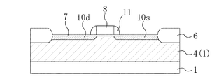
絶縁膜14の半導体層1側の表面は、ガラス基板22側へ窪んでおり、ゲート酸化膜7とLOCOS酸化膜6とが形成されている。ゲート酸化膜7と上記絶縁膜14との間には、ゲート電極8とサイドウォール11とが形成されている。サイドウォール11はゲート電極8の左右両側面にそれぞれ形成されている。
The surface of the insulating
上記絶縁膜21には、層間絶縁膜18との界面においてソース電極20s及びドレイン電極20dが形成されている。また、上記層間絶縁膜18、BPSG膜15、絶縁膜14及びゲート酸化膜7には、これらの各膜18,15,14,7を貫通するコンタクトホール19s,19dが形成され、導電性材料が充填されている。コンタクトホール19s内の導電性材料はソース電極20sと一体に形成される一方、コンタクトホール19d内の導電性材料はドレイン電極20dと一体に形成されている。
A
上記ゲート酸化膜7の表面には、半導体層1が形成されている。半導体層1は、シリコン層であって、例えばホウ素等のP型不純物が注入されたPウェル領域4と、活性領域40とにより構成されている。半導体層1は、LOCOS酸化膜6によって隣り合う他の半導体層(図示省略)との間が分離された状態で、絶縁膜である保護膜23により被覆されている。
A
半導体層1におけるガラス基板22側の表面は平面に形成される一方、保護膜23側の表面は、BPSG膜15の表面段差形状に沿って形成された表面を有している。つまり、半導体層1における保護膜23側の表面は、上記層間絶縁膜18とBPSG膜15との界面の形状と略同じなだらかな表面段差形状に形成されている。半導体層1は、このなだらかな段差形状の表面側において、剥離用物質がイオン注入されることにより形成されていた剥離層に沿って、その半導体層1の一部が分離されている。剥離用物質には、水素及び不活性ガス元素の少なくとも一方を適用することができる。
The surface of the
活性領域40は、チャネル領域41と、その左右両側に形成された低濃度不純物領域10s,10dと、さらにその左右両側に形成された高濃度不純物領域13s,13dとにより構成されている。上記低濃度不純物領域10s,10d及び高濃度不純物領域13s,13dには、例えばリン等のN型不純物が注入されている。低濃度不純物領域10s,10dは、いわゆるLDD領域を構成している。また、高濃度不純物領域13sはソース領域を構成する一方、高濃度不純物領域13dはドレイン領域を構成している。
The
チャネル領域41は、ゲート酸化膜7を介して上記ゲート電極8に対向して形成されている。また、低濃度不純物領域10s,10dは、ゲート酸化膜7を介して上記サイドウォール11に対向して形成されている。そして、高濃度不純物領域13sにはコンタクトホール19sを介してソース電極20sが接続される一方、高濃度不純物領域13dにはコンタクトホール19dを介してソース電極20sが接続されている。
The
こうして、ガラス基板22にはMOSトランジスタであるTFT50が形成され、半導体層1は、ゲート電極8に対向している領域(つまりチャネル領域41)が比較的薄く形成される一方、その他の領域(例えば高濃度不純物領域13s,13d)が比較的厚く形成されている。さらに、BPSG膜15は、ゲート電極8及び半導体層1を覆うように形成され、ゲート電極8の表面と半導体層1の表面とに対応して形成されて急峻な傾斜面を含む表面段差形状を、なだらかな表面段差形状に補償するように構成されている。
Thus, the
−製造方法−
次に、本発明に係る半導体装置の製造方法について説明する。
-Manufacturing method-
Next, a method for manufacturing a semiconductor device according to the present invention will be described.
本実施形態の製造方法には、酸化膜形成工程と、ゲート電極形成工程と、活性領域形成工程と、絶縁膜形成工程と、剥離層形成工程と、平坦化膜形成工程と、接合工程と、分離工程と、保護膜形成工程とが含まれる。 The manufacturing method of the present embodiment includes an oxide film forming step, a gate electrode forming step, an active region forming step, an insulating film forming step, a release layer forming step, a planarizing film forming step, a bonding step, A separation step and a protective film formation step are included.
すなわち、酸化膜形成工程では、半導体基板1(上述の半導体層1に相当する)にPウェル領域4を形成すると共に、LOCOS酸化膜6及びゲート酸化膜7を形成する。図2に示すように、まず、シリコン基板である半導体基板1に熱酸化膜2を形成し、P型不純物元素3(例えばホウ素)を半導体基板1の内部にイオン注入する。続いて、図3に示すように、上記半導体基板1に熱処理を行い、イオン注入されたP型不純物元素3を拡散すると共に活性化させることによって、Pウェル領域4を形成する。
That is, in the oxide film forming step, the
次に、図4に示すように、熱酸化膜2の表面に窒化珪素膜5を形成した後に、後工程で活性領域40を形成する領域に窒化珪素膜5をパターニングして残す。続いて、熱酸化膜2及び半導体基板1に対してLOCOS酸化を行い、図5に示すように、窒化珪素膜5の左右両側にLOCOS酸化膜6を形成する。次に、図6に示すように、窒化珪素膜5及び熱酸化膜2を一旦除去した後に、熱酸化膜2が形成されていた領域にゲート酸化膜7を形成する。
Next, as shown in FIG. 4, after the
次に行うゲート電極形成工程では、図7に示すように、ゲート酸化膜7の表面に積層した導電性材料をフォトリソグラフィ法等によりパターニングして、後にNMOSトランジスタ(つまりTFT50)を構成するゲート電極8を半導体基板1に形成する。
In the next gate electrode formation step, as shown in FIG. 7, the conductive material laminated on the surface of the
次に、活性領域形成工程では、上記半導体基板1のPウェル領域4に活性領域40を形成する。すなわち、図8に示すように、まず、ゲート電極8をマスクとして、リン等のN型不純物元素9をイオン注入し、N型低濃度不純物領域10s,10dを形成する。続いて、ゲート酸化膜7の表面にCVD等によりSiO2膜を形成した後、異方性ドライエッチングを行うことにより、図9に示すように、ゲート電極8の両側壁にサイドウォール11を形成する。
Next, in the active region forming step, an
続いて、図10に示すように、ゲート電極8及びサイドウォール11をマスクとして、リン等のN型不純物元素12をイオン注入することにより、N型高濃度不純物領域13s,13dを形成する。その結果、低濃度不純物領域10s,10dは、ゲート酸化膜7を介してサイドウォール11に対向する領域に形成されることとなる。その後、図11に示すように、SiO2等の絶縁膜14を形成した後に、上記低濃度不純物領域10s,10d及び高濃度不純物領域13s,13dに対して熱処理を行い、イオン注入した不純物元素の活性化を行う。このことにより、LDD領域を有する活性領域40を形成する。
Subsequently, as shown in FIG. 10, N-type high-
次に行う絶縁膜形成工程では、図11に示すように、絶縁膜14の表面に絶縁膜であるBPSG膜15を積層した後に、このBPSG膜15に対して900℃以上の温度で熱処理を行う。このことにより、BPSG膜15の表面段差形状をなだらかにしてBPSGリフロー膜15を形成する。尚、上記N型不純物の活性化は、BPSG膜15の熱処理と兼ねて行うようにしてもよい。
In the next insulating film forming step, as shown in FIG. 11, after the
このことにより、半導体基板1の表面とゲート電極8の表面とに対応して形成される比較的急峻な表面段差形状を、BPSG膜15のなだらかな表面段差形状に補償する。このとき、半導体基板1の表面に対するBPSG膜15の最大傾斜角度θを0°<θ≦50°の範囲に規定する。
Thus, the relatively steep surface step shape formed corresponding to the surface of the
すなわち、BPSG膜15における表面段差形状は、仮に、その最大傾斜角度θが50°よりも大きいと、剥離層17の段差形状が急峻に変化することとなるため、後の分離工程において、半導体基板1の一部が予期せぬ位置で分離してしまい、半導体基板1の一部を剥離層17に沿って分離させることができない。一方、最大傾斜角度θが0°では、絶縁膜の表面をなだらかな表面段差形状に形成することができない。したがって、最大傾斜角度θは0°<θ≦50°に規定することによって、なだらかな表面段差形状の剥離層17に沿って、半導体基板1の一部を剥離させることが可能となる。
That is, if the maximum step angle θ of the
次に、剥離層形成工程では、図12に示すように、上記半導体層1のPウェル領域に対し、上記BPSG膜15を介して水素や、He及びNe等の不活性ガス元素からなる剥離用物質16をイオン注入することにより、剥離層17を形成する。このとき、剥離用物質16は、なだらかなBPSG膜15の表面形状に沿った深さ位置に注入されるため、剥離層17は、その深さ位置がなだらかに変化するように形成される。
Next, in the peeling layer forming step, as shown in FIG. 12, the P well region of the
次に、平坦化膜形成工程では、図13に示すように、半導体基板1及びBPSG膜15を覆うようにSiO2膜を形成し、CMP(Chemical Mechanical Polishing)等により平坦化することにより、層間絶縁膜18を形成する。
Next, in the planarization film forming step, as shown in FIG. 13, an SiO 2 film is formed so as to cover the
続いて、図14に示すように、ソース電極20s及びドレイン電極20dを形成する。すなわち、上記層間絶縁膜18、BPSG膜15、絶縁膜14、及びゲート酸化膜7を貫通するコンタクトホール19s,19dを形成する。コンタクトホール19sは、上記高濃度不純物領域(ソース領域)13sの上方位置に形成する一方、コンタクトホール19dは、上記高濃度不純物領域(ドレイン領域)13dの上方位置に形成する。そして、電極材料である導電性材料を、上記コンタクトホール19s,19dの内部と層間絶縁膜18の表面とに設けた後にパターニングすることによって、コンタクトホール19sの上方位置にソース電極20sを形成する一方、コンタクトホール19dの上方位置にドレイン電極20dを形成する。その後、絶縁膜21を形成した後に、CMP等により表面を平坦化する。
Subsequently, as shown in FIG. 14, a
次に、接合工程において、図15に示すように、絶縁膜21の表面を洗浄した後に、その平坦化された表面にガラス基板22を接合する。
Next, in the bonding step, as shown in FIG. 15, after the surface of the insulating
次に行う分離工程では、図16に示すように、400〜600℃程度の温度で熱処理を行う。このことにより、Pウェル領域4を含む半導体基板1の一部を剥離層17に沿って分離して、TFT50をガラス基板22の上に移す。尚、本実施形態では、分離工程において一部が分離された半導体基板1を、半導体層1と称する。
In the next separation step, heat treatment is performed at a temperature of about 400 to 600 ° C. as shown in FIG. Thereby, a part of the
次に、保護膜形成工程では、図17に示すように、剥離層17をエッチング等により取り除いた後、チャネル領域41の薄膜化すると共に、LOCOS酸化膜6を露出させて素子分離を行うために、半導体層1をエッチングする。その後、露出した半導体層1の表面を保護し、電気絶縁性を確保するため、保護膜である絶縁膜23を形成する。以上の工程によりガラス基板22上にTFT50を製造する。
Next, in the protective film forming step, as shown in FIG. 17, after removing the
−実施形態1の効果−
したがって、この実施形態1によると、半導体基板1の表面とゲート電極8の表面とに対応して形成される表面段差形状が急峻であっても、これら半導体基板1及びゲート電極8を絶縁膜であるBPSG膜15によって覆うことにより、その急峻な表面段差形状をなだらかな表面段差形状に補償することができる。そのことにより、剥離用物質16は、半導体基板1に対し、なだらかなBPSG膜15の表面形状に沿った深さ位置に注入されるため、剥離層17の深さ位置をなだらかに変化させることができる。その結果、剥離層17の深さ位置(言い換えれば段差形状)を急峻に変化させないようにすることができるため、半導体基板1の一部を、剥離層17に沿って確実に剥離することができる。
-Effect of Embodiment 1-
Therefore, according to the first embodiment, even if the surface step shape formed corresponding to the surface of the
さらに、剥離層17の深さ位置を、ゲート電極8に対向する領域(つまりチャネル領域41)では浅く形成すると共に、その他の領域(例えばソース領域13s及びドレイン領域13d)では深く形成することができるため、チャネル領域41を比較的薄くする一方、ソース領域13s及びドレイン領域13dを比較的厚く形成することできる。その結果、完全空乏型のSOI動作を可能としつつソース領域13s及びドレイン領域13dにおけるシート抵抗を低減できるため、TFT50の特性を向上させることができる。
Furthermore, the depth of the
ところで、例えばフォトリソグラフィ法等の非自己整合法(ノンセルフアライン)により、チャネル領域41を部分的に薄膜化して形成しようとすると、その薄膜化しようとする半導体層1の領域と、ゲート電極8を形成する領域との間で、位置ずれが必然的に生じてしまう。そのため、位置ずれを考慮したマージンを設ける必要があるため、素子寸法の増大を招く結果となる。この問題は、ゲート長が短くなるほど顕著となり、素子の集積度が低下すると共に、トランジスタ特性のばらつきの要因ともなるので、上記非自己整合法を適用することは望ましくない。
By the way, if the
これに対し、本実施形態では、チャネル領域41の薄膜化を自己整合的(セルフアライン)により形成できるため、上述の問題は生じない。すなわち、位置ずれを考慮したマージンを設ける必要がないため、素子寸法を縮小して素子の集積度を向上させると共にトランジスタ特性のばらつきを抑制することができる。
On the other hand, in the present embodiment, since the
《発明の実施形態2》
図17は、本発明の実施形態2を示している。尚、以降の各実施形態では、図1〜図16と同じ部分については同じ符号を付して、その詳細な説明を省略する。
<<
FIG. 17 shows a second embodiment of the present invention. In the following embodiments, the same parts as those in FIGS. 1 to 16 are denoted by the same reference numerals, and detailed description thereof is omitted.
本実施形態のTFT50は、ソース電極20sがガラス基板22に予め形成されていた電気素子27である能動素子及び受動素子の少なくとも一方に対して電気的に接続されている。
In the
すなわち、図17に示すように、ガラス基板22へ移されたTFT50は、ガラス基板22の表面に形成された絶縁膜26と共に保護膜23により被覆されている。また、ソース電極20sは、側方へ延長されている。上記ソース電極20sの延長部分の上方位置には、層間絶縁膜18、BPSG膜15、絶縁膜14、LOCOS酸化膜6及び保護膜23を貫通するコンタクトホール24aが形成されている。
That is, as shown in FIG. 17, the
一方、ガラス基板22に形成された電気素子27の上方位置には、保護膜23を貫通するコンタクトホール24bが形成されている。そして、金属材料等が、上記各コンタクトホール24a,24b内に充填されると共に保護膜23の表面にパターンニングされてメタル配線25が形成されている。こうして、上記ソース電極20sと電気素子27とは、メタル配線25を介して電気的に接続されている。
On the other hand, a
本実施形態のTFT50を製造する方法は、素子形成工程と、接続工程とを備えている。すなわち、素子形成工程は、上記実施形態1で説明した接合工程よりも前に行われ、ガラス基板22に絶縁膜26を積層し、その絶縁膜26の表面に電気素子27を予め形成しておく。そして、接続工程は、上記接合工程よりも後に行われ、上記電気素子27を、活性領域40のソース領域13sに対し、メタル配線25及びソース電極20sを介して電気的に接続する。
The method for manufacturing the
尚、電気素子27に接続する対象は、ソース電極20sに限らずドレイン電極20dや、図示を省略しているが、メタル配線層を介したゲート電極28であってもよいのは勿論である。
Note that the target to be connected to the
《発明の実施形態3》
図18〜図20は、本発明の実施形態3を示している。
<< Embodiment 3 of the Invention >>
18 to 20 show Embodiment 3 of the present invention.
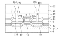
本実施形態のTFT50は、図20に示すように、BPSG膜15が少なくともゲート電極8を覆っている部分において薄膜化して形成されている。すなわち、BPSG膜15の表面段差形状は、薄膜化されることにより修正され、チャネル領域41に対向するBPSG膜15の表面が、半導体層1側に近付けられている。このことにより、本実施形態では、ソース領域13s及びドレイン領域13dにおけるBPSG膜15の厚みと、チャネル領域41におけるBPSG膜15の厚みとの差が、上記実施形態1に比べて小さくなっている。
As shown in FIG. 20, the
本実施形態のTFT50を製造する方法には、薄膜化工程が含まれる。
The method for manufacturing the
薄膜化工程は、上記実施形態1における絶縁膜形成工程の後に行う。そして、図18に示すように、CMP法によりBPSG膜15における少なくともゲート電極8を覆っている部分を薄膜化する。このことにより、チャネル領域41におけるBPSG膜15の表面の高さと、ソース領域13s及びドレイン領域13dにおけるBPSG膜15の表面の高さとの差を小さく調整することが可能となる。
The thinning process is performed after the insulating film forming process in the first embodiment. Then, as shown in FIG. 18, the portion of the
続いて、剥離層形成工程において、図19に示すように、厚みが部分的に小さくなったBPSG膜15を介して水素や、He及びNe等の不活性ガス元素からなる剥離用物質16をイオン注入することにより、剥離層17を形成する。その後、上記実施形態1と同様に、平坦化膜形成工程、接合工程、分離工程、及び保護膜形成工程を経て、図20に示すように、TFT50を製造する。
Subsequently, in the release layer forming step, as shown in FIG. 19, the
したがって、本実施形態によると、上記実施形態1と同様の効果が得れることに加え、チャネル領域41と、ソース領域13s及びドレイン領域13dとにそれぞれ形成される剥離層17の高さの差を調整して小さくすることができるので、ゲート電極8の厚みに拘わらず、ガラス基板22に形成されるTFT50のチャネル領域41とソース領域13s及びドレイン領域13dとにおける半導体層1の厚みの差を最適値に調整することが可能となる。その結果、トランジスタ特性の最適化を図ることができる。
Therefore, according to the present embodiment, in addition to obtaining the same effects as those of the first embodiment, the difference in height between the
《発明の実施形態4》
図21〜図23は、本発明の実施形態4を示している。
<<
21 to 23
上記実施形態1では、半導体基板1上の表面段差形状を補償するための絶縁膜として、BPSG膜15を適用したのに対し、本実施形態では、SOG(Spin On Glass)膜30を適用している。したがって、半導体基板1上の急峻な表面段差形状は、SOG膜30によってなだらかな表面段差形状に補償されている。
In the first embodiment, the
本実施形態のTFT50を製造する場合には、図21に示すように、上記実施形態1における絶縁膜形成工程において、絶縁膜14の表面にSOG膜30を塗布して形成する。このことにより、硬化前のSOG膜30が流動性を有しているため、ゲート電極8上の段差形状を容易な方法でなだらかに形成できると共に、その段差自体を小さくすることができる。
When manufacturing the
続いて、剥離層形成工程において、図22に示すように、厚みが部分的に小さくなったSOG膜30を介して水素や、He及びNe等の不活性ガス元素からなる剥離用物質16をイオン注入することにより、剥離層17を形成する。その後、上記実施形態1と同様に、平坦化膜形成工程、接合工程、分離工程、及び保護膜形成工程を経て、図23に示すように、TFT50を製造する。
Subsequently, in the release layer forming step, as shown in FIG. 22, the
したがって、本実施形態によると、上記実施形態1と同様の効果を得ることができる。さらに、なだらかな表面段差形状を容易に形成することができる。 Therefore, according to the present embodiment, the same effect as in the first embodiment can be obtained. Furthermore, a gentle surface step shape can be easily formed.
《発明の実施形態5》
図24〜図26は、本発明の実施形態5を示している。
<<
24 to 26 show a fifth embodiment of the present invention.
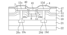
本実施形態のTFT50は、図26に示すように、BPSG膜15の表面が、ソース領域13s及びドレイン領域13dに対向する部分において高く形成されている。すなわち、ソース領域13s及びドレイン領域13dに対向する部分では、絶縁膜14の表面にBPSG膜15を嵩増しするためのダミーパターン34が形成されている。
As shown in FIG. 26, the
このことにより、ソース領域13s及びドレイン領域13dに対向するBPSG膜15の表面が半導体基板1とは反対側へ移動するため、半導体基板1の表面とゲート電極8の表面とに対応して形成される表面段差形状は、BPSG膜15によってなだらかな表面段差形状に補償されている。
As a result, the surface of the
本実施形態のTFT50を製造する場合には、上記実施形態1における絶縁膜形成工程の前に、ダミーパターン形成工程を行う。このダミーパターン形成工程では、図24に示すように、半導体基板1の上である絶縁膜14の表面に対し、例えばSiO2の膜を形成した後に、フォトリソグラフィ法等によりパターニングしてダミーパターン34を形成する。
When manufacturing the
続いて、絶縁膜形成工程では、上記ダミーパターン34、ゲート電極8及び半導体基板1を覆うように、BPSG膜15を形成すると共に、900℃以上の温度で熱処理を行うことにより、図25に示すように、BPSG膜15の表面をなだらかな表面段差形状にする。
Subsequently, in the insulating film forming step, a
次に、剥離層形成工程において、図26に示すように、ソース領域13s及びドレイン領域13dに対向する領域において表面が部分的に高くなったBPSG膜15を介して水素や、He及びNe等の不活性ガス元素からなる剥離用物質16をイオン注入することにより、剥離層17を形成する。その後、上記実施形態1と同様に、平坦化膜形成工程、接合工程、分離工程、及び保護膜形成工程を経てTFT50を製造する。
Next, in the peeling layer forming step, as shown in FIG. 26, hydrogen, He, Ne, or the like is formed through the
したがって、この実施形態によると、上記実施形態3と同様に、チャネル領域41と、ソース領域13s及びドレイン領域13dとにそれぞれ形成される剥離層17の高さの差を調整して小さくすることができるので、ゲート電極8の厚みに拘わらず、ガラス基板22に形成されるTFT50のチャネル領域41とソース領域13s及びドレイン領域13dとにおける半導体層1の厚みの差を最適値に調整することが可能となる。その結果、トランジスタ特性の最適化を図ることができる。
Therefore, according to this embodiment, as in the third embodiment, the height difference between the
以上説明したように、本発明は、半導体装置の製造方法及び半導体装置並びに液晶表示装置について有用であり、特に、半導体基板に対し、その一部を剥離層に沿って確実に剥離すると共に、ゲート電極に対向する領域では比較的薄くする一方、その他の領域では比較的厚く形成することにより、半導体装置の特性を向上させる場合に適している。 As described above, the present invention is useful for a semiconductor device manufacturing method, a semiconductor device, and a liquid crystal display device. In particular, a part of a semiconductor substrate is reliably peeled off along a peeling layer, and a gate is also provided. This is suitable for improving the characteristics of the semiconductor device by forming the film relatively thin in the region facing the electrode and relatively thick in the other regions.
S 液晶表示装置
θ 絶縁膜の最大傾斜角度
1 半導体基板(半導体層)
7 ゲート酸化膜
15 BPSG膜(絶縁膜)
16 剥離用物質
17 剥離層
18 層間絶縁膜(第2の平坦化膜)
21 絶縁膜(第1の平坦化膜)
22 ガラス基板(基板)
27 電気素子(能動素子、受動素子)
30 SOG膜
34 ダミーパターン
40 活性領域
50 TFT(半導体装置、薄膜トランジスタ)
52 アクティブマトリクス基板
S Liquid crystal display device θ Maximum inclination angle of insulating
7
16
21 Insulating film (first planarizing film)
22 Glass substrate (substrate)
27 Electric elements (active elements, passive elements)
30
52 Active matrix substrate
Claims (26)
上記半導体基板の表面とゲート電極の表面とに対応して形成される表面段差形状をなだらかな表面段差形状に補償するための絶縁膜を、上記ゲート電極及び上記半導体基板を覆うように形成する絶縁膜形成工程と、
上記半導体基板に対し、上記絶縁膜を介して剥離用物質をイオン注入することにより、剥離層を形成する剥離層形成工程と、
上記半導体基板の一部を上記剥離層に沿って分離する分離工程とを備えている
ことを特徴とする半導体装置の製造方法。 Forming a gate electrode on a semiconductor substrate; and
An insulating film for covering the gate electrode and the semiconductor substrate with an insulating film for compensating the surface step shape formed corresponding to the surface of the semiconductor substrate and the surface of the gate electrode with a gentle surface step shape. A film forming step;
A release layer forming step for forming a release layer by ion-implanting a release material to the semiconductor substrate through the insulating film;
And a separation step of separating a part of the semiconductor substrate along the release layer.
上記絶縁膜は、上記半導体基板の表面に対する最大傾斜角度θが、0°<θ≦50°の範囲に規定されている
ことを特徴とする半導体装置の製造方法。 In claim 1,
The method of manufacturing a semiconductor device, wherein the insulating film has a maximum inclination angle θ with respect to the surface of the semiconductor substrate in a range of 0 ° <θ ≦ 50 °.
上記絶縁膜形成工程の後に行われ、上記絶縁膜における上記ゲート電極を覆っている部分を薄膜化する薄膜化工程を含む
ことを特徴とする半導体装置の製造方法。 In claim 1,
A method for manufacturing a semiconductor device, comprising: a thinning step performed after the insulating film forming step and thinning a portion of the insulating film covering the gate electrode.
上記半導体基板及び上記絶縁膜を覆う平坦化膜を形成する平坦化膜形成工程と、
上記平坦化膜に基板を接合する接合工程とを備え、
上記接合工程は、上記分離工程よりも前に行われる
ことを特徴とする半導体装置の製造方法。 In claim 1,
A planarization film forming step of forming a planarization film covering the semiconductor substrate and the insulating film;
A bonding step of bonding the substrate to the planarizing film,
The method for manufacturing a semiconductor device, wherein the bonding step is performed before the separation step.
上記基板は透明基板である
ことを特徴とする半導体装置の製造方法。 In claim 4,
A method of manufacturing a semiconductor device, wherein the substrate is a transparent substrate.
上記半導体基板はシリコン基板である
ことを特徴とする半導体装置の製造方法。 In claim 1,
A method of manufacturing a semiconductor device, wherein the semiconductor substrate is a silicon substrate.
上記剥離用物質は、水素及び不活性ガス元素の少なくとも一方である
ことを特徴とする半導体装置の製造方法。 In claim 1,
The method for manufacturing a semiconductor device, wherein the peeling material is at least one of hydrogen and an inert gas element.
上記ゲート電極は、MOSトランジスタを構成する
ことを特徴とする半導体装置の製造方法。 In claim 1,
A method of manufacturing a semiconductor device, wherein the gate electrode constitutes a MOS transistor.
上記絶縁膜は、BPSG(Borophosphosilicate glass)膜である
ことを特徴とする半導体装置の製造方法。 In claim 1,
The method of manufacturing a semiconductor device, wherein the insulating film is a BPSG (Borophosphosilicate glass) film.
上記BPSG膜は、上記絶縁膜形成工程において900℃以上の温度で熱処理される
ことを特徴とする半導体装置の製造方法。 In claim 9,
The BPSG film is heat-treated at a temperature of 900 ° C. or higher in the insulating film formation step.
上記絶縁膜は、SOG(Spin On Glass)膜である
ことを特徴とする半導体装置の製造方法。 In claim 1,
The method for manufacturing a semiconductor device, wherein the insulating film is a SOG (Spin On Glass) film.
上記絶縁膜形成工程の前に行われ、上記ゲート電極に重ならないようにダミーパターンを形成するダミーパターン形成工程を備え、
上記絶縁膜形成工程では、上記ダミーパターン、上記ゲート電極及び上記半導体基板を覆うように、上記絶縁膜を形成する
ことを特徴とする半導体装置。 In claim 1,
A dummy pattern forming step that is performed before the insulating film forming step and forms a dummy pattern so as not to overlap the gate electrode;
In the insulating film forming step, the insulating film is formed so as to cover the dummy pattern, the gate electrode, and the semiconductor substrate.
上記接合工程よりも前に行われ、上記基板に能動素子及び受動素子の少なくとも一方を予め形成する素子形成工程と、
上記ゲート電極が形成された半導体基板に活性領域を形成する活性領域形成工程と、
上記接合工程よりも後に行われ、上記活性領域と、上記基板に形成されている能動素子及び受動素子の少なくとも一方とを電気的に接続する接続工程とを備えている
ことを特徴とする半導体装置の製造方法。 In claim 4,
An element forming step that is performed prior to the bonding step, and in which at least one of an active element and a passive element is formed in advance on the substrate;
An active region forming step of forming an active region in the semiconductor substrate on which the gate electrode is formed;
A semiconductor device comprising a connection step that is performed after the bonding step and electrically connects the active region and at least one of an active element and a passive element formed on the substrate. Manufacturing method.
上記半導体層に形成されたゲート電極と、
上記ゲート電極及び上記半導体層を覆うように形成され、上記ゲート電極の表面と半導体層の表面とに対応して形成される表面段差形状をなだらかな表面段差形状に補償するための絶縁膜とを備え、
上記半導体層は、上記絶縁膜の表面段差形状に沿って形成された表面を有している
ことを特徴とする半導体装置。 A semiconductor layer;
A gate electrode formed in the semiconductor layer;
An insulating film formed so as to cover the gate electrode and the semiconductor layer, and for compensating the surface step shape formed corresponding to the surface of the gate electrode and the surface of the semiconductor layer to a gentle surface step shape; Prepared,
The semiconductor device, wherein the semiconductor layer has a surface formed along a surface step shape of the insulating film.
上記半導体層の一部は、剥離物質がイオン注入されることにより形成された剥離層に沿って分離されている
ことを特徴とする半導体装置。 In claim 14,
A part of the semiconductor layer is separated along a peeling layer formed by ion implantation of a peeling substance.
上記絶縁膜は、上記半導体層の表面に対する最大傾斜角度θが、0°<θ≦50°の範囲に規定されている
ことを特徴とする半導体装置。 In claim 14,
The semiconductor device, wherein the insulating film has a maximum inclination angle θ with respect to the surface of the semiconductor layer in a range of 0 ° <θ ≦ 50 °.
上記絶縁膜は、上記ゲート電極を覆っている部分が薄膜化して形成されている
ことを特徴とする半導体装置。 In claim 14,
The semiconductor device according to claim 1, wherein the insulating film is formed by thinning a portion covering the gate electrode.
上記半導体層及び上記絶縁膜を覆う平坦化膜と、
上記平坦化膜の表面に接合された基板とを備えている
ことを特徴とする半導体装置。 In claim 14,
A planarization film covering the semiconductor layer and the insulating film;
And a substrate bonded to the surface of the planarizing film.
上記基板は透明基板である
ことを特徴とする半導体装置。 In claim 18,
A semiconductor device, wherein the substrate is a transparent substrate.
上記半導体層はシリコン層である
ことを特徴とする半導体装置。 In claim 14,
A semiconductor device, wherein the semiconductor layer is a silicon layer.
上記剥離用物質は、水素及び不活性ガス元素の少なくとも一方である
ことを特徴とする半導体装置。 In claim 14,
The semiconductor device, wherein the peeling material is at least one of hydrogen and an inert gas element.
上記ゲート電極は、MOSトランジスタを構成している
ことを特徴とする半導体装置。 In claim 14,
The semiconductor device, wherein the gate electrode constitutes a MOS transistor.
上記絶縁膜は、BPSG(Borophosphosilicate glass)膜である
ことを特徴とする半導体装置。 In claim 14,
The semiconductor device is characterized in that the insulating film is a BPSG (Borophosphosilicate glass) film.
上記BPSG膜は、900℃以上の温度で熱処理されている
ことを特徴とする半導体装置。 In claim 14,
The semiconductor device, wherein the BPSG film is heat-treated at a temperature of 900 ° C. or higher.
上記半導体層には、活性領域が形成され、
上記基板には、能動素子及び受動素子の少なくとも一方が、上記活性領域に電気的に接続して形成されている
ことを特徴とする半導体装置。 In claim 18,
An active region is formed in the semiconductor layer,
A semiconductor device, wherein at least one of an active element and a passive element is formed on the substrate so as to be electrically connected to the active region.
上記薄膜トランジスタは、半導体層と、上記半導体層に形成されたゲート電極と、上記ゲート電極及び上記半導体層を覆うように形成され、上記ゲート電極の表面と半導体層の表面とに対応して形成される表面段差形状をなだらかな表面段差形状に補償するための絶縁膜とを備え、
上記半導体層は、上記絶縁膜の表面段差形状に沿って形成された表面を有している
ことを特徴とする液晶表示装置。 A liquid crystal display device having an active matrix substrate on which a plurality of thin film transistors are formed,
The thin film transistor is formed to cover a semiconductor layer, a gate electrode formed on the semiconductor layer, the gate electrode and the semiconductor layer, and corresponding to a surface of the gate electrode and a surface of the semiconductor layer. And an insulating film for compensating the surface step shape to a gentle surface step shape,
The liquid crystal display device, wherein the semiconductor layer has a surface formed along a surface step shape of the insulating film.
Priority Applications (1)
| Application Number | Priority Date | Filing Date | Title |
|---|---|---|---|
| JP2005110250A JP4943663B2 (en) | 2005-04-06 | 2005-04-06 | Semiconductor device manufacturing method, semiconductor device, and liquid crystal display device |
Applications Claiming Priority (1)
| Application Number | Priority Date | Filing Date | Title |
|---|---|---|---|
| JP2005110250A JP4943663B2 (en) | 2005-04-06 | 2005-04-06 | Semiconductor device manufacturing method, semiconductor device, and liquid crystal display device |
Publications (2)
| Publication Number | Publication Date |
|---|---|
| JP2006294703A true JP2006294703A (en) | 2006-10-26 |
| JP4943663B2 JP4943663B2 (en) | 2012-05-30 |
Family
ID=37414977
Family Applications (1)
| Application Number | Title | Priority Date | Filing Date |
|---|---|---|---|
| JP2005110250A Expired - Fee Related JP4943663B2 (en) | 2005-04-06 | 2005-04-06 | Semiconductor device manufacturing method, semiconductor device, and liquid crystal display device |
Country Status (1)
| Country | Link |
|---|---|
| JP (1) | JP4943663B2 (en) |
Cited By (3)
| Publication number | Priority date | Publication date | Assignee | Title |
|---|---|---|---|---|
| JP2009004739A (en) * | 2007-05-18 | 2009-01-08 | Semiconductor Energy Lab Co Ltd | Manufacturing method of soi substrate and manufacturing method of semiconductor device |
| US8288184B2 (en) | 2007-12-18 | 2012-10-16 | Sharp Kabushiki Kaisha | Production method of semiconductor device and semiconductor device |
| JP2018522397A (en) * | 2015-05-08 | 2018-08-09 | クアルコム,インコーポレイテッド | Fabrication of junction semiconductor structure using etch stop region |
Citations (11)
| Publication number | Priority date | Publication date | Assignee | Title |
|---|---|---|---|---|
| JPH0541478A (en) * | 1991-07-22 | 1993-02-19 | Nec Corp | Semiconductor device and manufacture thereof |
| JPH06224189A (en) * | 1993-01-21 | 1994-08-12 | Handotai Process Kenkyusho:Kk | Method and apparatus for forming flattened film |
| JPH0737886A (en) * | 1993-07-19 | 1995-02-07 | Nec Corp | Manufacture of semiconductor device |
| JPH08288295A (en) * | 1995-04-18 | 1996-11-01 | Sony Corp | Manufacture of semiconductor device |
| JPH10125881A (en) * | 1996-10-18 | 1998-05-15 | Sony Corp | Laminated soi substrate, its forming method and mos transistor formed on the substrate |
| JPH1124106A (en) * | 1997-07-03 | 1999-01-29 | Seiko Epson Corp | Substrate for liquid crystal panel, liquid crystal panel, and their manufacture |
| JPH11243209A (en) * | 1998-02-25 | 1999-09-07 | Seiko Epson Corp | Transfer method of thin-film device, the thin-film device, thin-film integrated circuit device, active matrix substrate, liquid crystal display device, and electronic apparatus |
| JP2001508943A (en) * | 1997-01-27 | 2001-07-03 | コミツサリア タ レネルジー アトミーク | Method for obtaining a thin film, in particular comprising a semiconductor film, comprising an ion implantation step and having a region protected from ions |
| JP2002343972A (en) * | 2001-05-15 | 2002-11-29 | Sony Corp | Method of manufacturing semiconductor device |
| JP2004288780A (en) * | 2003-03-20 | 2004-10-14 | Sharp Corp | Semiconductor device and its manufacturing method |
| JP2005056917A (en) * | 2003-08-05 | 2005-03-03 | Sharp Corp | Process for fabricating semiconductor device |
-
2005
- 2005-04-06 JP JP2005110250A patent/JP4943663B2/en not_active Expired - Fee Related
Patent Citations (11)
| Publication number | Priority date | Publication date | Assignee | Title |
|---|---|---|---|---|
| JPH0541478A (en) * | 1991-07-22 | 1993-02-19 | Nec Corp | Semiconductor device and manufacture thereof |
| JPH06224189A (en) * | 1993-01-21 | 1994-08-12 | Handotai Process Kenkyusho:Kk | Method and apparatus for forming flattened film |
| JPH0737886A (en) * | 1993-07-19 | 1995-02-07 | Nec Corp | Manufacture of semiconductor device |
| JPH08288295A (en) * | 1995-04-18 | 1996-11-01 | Sony Corp | Manufacture of semiconductor device |
| JPH10125881A (en) * | 1996-10-18 | 1998-05-15 | Sony Corp | Laminated soi substrate, its forming method and mos transistor formed on the substrate |
| JP2001508943A (en) * | 1997-01-27 | 2001-07-03 | コミツサリア タ レネルジー アトミーク | Method for obtaining a thin film, in particular comprising a semiconductor film, comprising an ion implantation step and having a region protected from ions |
| JPH1124106A (en) * | 1997-07-03 | 1999-01-29 | Seiko Epson Corp | Substrate for liquid crystal panel, liquid crystal panel, and their manufacture |
| JPH11243209A (en) * | 1998-02-25 | 1999-09-07 | Seiko Epson Corp | Transfer method of thin-film device, the thin-film device, thin-film integrated circuit device, active matrix substrate, liquid crystal display device, and electronic apparatus |
| JP2002343972A (en) * | 2001-05-15 | 2002-11-29 | Sony Corp | Method of manufacturing semiconductor device |
| JP2004288780A (en) * | 2003-03-20 | 2004-10-14 | Sharp Corp | Semiconductor device and its manufacturing method |
| JP2005056917A (en) * | 2003-08-05 | 2005-03-03 | Sharp Corp | Process for fabricating semiconductor device |
Cited By (4)
| Publication number | Priority date | Publication date | Assignee | Title |
|---|---|---|---|---|
| JP2009004739A (en) * | 2007-05-18 | 2009-01-08 | Semiconductor Energy Lab Co Ltd | Manufacturing method of soi substrate and manufacturing method of semiconductor device |
| US8895407B2 (en) | 2007-05-18 | 2014-11-25 | Semiconductor Energy Laboratory Co., Ltd. | Manufacturing method of SOI substrate and manufacturing method of semiconductor device |
| US8288184B2 (en) | 2007-12-18 | 2012-10-16 | Sharp Kabushiki Kaisha | Production method of semiconductor device and semiconductor device |
| JP2018522397A (en) * | 2015-05-08 | 2018-08-09 | クアルコム,インコーポレイテッド | Fabrication of junction semiconductor structure using etch stop region |
Also Published As
| Publication number | Publication date |
|---|---|
| JP4943663B2 (en) | 2012-05-30 |
Similar Documents
| Publication | Publication Date | Title |
|---|---|---|
| JP4467628B2 (en) | Manufacturing method of semiconductor device | |
| JP5057981B2 (en) | Semiconductor device, manufacturing method thereof, and display device | |
| US7166514B2 (en) | Semiconductor device and method of manufacturing the same | |
| TWI328268B (en) | Semiconductor device and forming method thereof | |
| JP2009027008A (en) | Semiconductor device, and manufacturing method thereof | |
| JP2005228762A (en) | Semiconductor device and its manufacturing method | |
| US20070020828A1 (en) | Method for manufacturing semiconductor apparatus and the semiconductor apparatus | |
| US7838936B2 (en) | Semiconductor device and manufacturing method thereof, and liquid crystal display device | |
| JP4943663B2 (en) | Semiconductor device manufacturing method, semiconductor device, and liquid crystal display device | |
| JP4175650B2 (en) | Manufacturing method of semiconductor device | |
| JP5074523B2 (en) | Semiconductor device and manufacturing method thereof | |
| US6764921B2 (en) | Semiconductor device and method for fabricating the same | |
| WO2009113427A1 (en) | Semiconductor device, semiconductor device manufacturing method and display device | |
| JP2002270851A (en) | Method for fabricating semiconductor device | |
| JP2005109203A (en) | Semiconductor substrate, method of manufacturing the same semiconductor device, and method of manufacturing the same | |
| JP2007234628A (en) | Semiconductor device, and its manufacturing method | |
| JPH0794722A (en) | Mos transistor with stacked diffused layers and its manufacturing method | |
| US8232213B2 (en) | Semiconductor device and manufacturing method thereof, and liquid crystal display device | |
| JP2001298195A (en) | Mos transistor | |
| JPH1168094A (en) | Manufacture of semiconductor integrated circuit device | |
| JP2008205104A (en) | Method for fabricating semiconductor device | |
| JP4942951B2 (en) | MOS type transistor manufacturing method and MOS type transistor | |
| JP2007335837A (en) | Manufacturing method of semiconductor device | |
| JP2008066566A (en) | Semiconductor device, and its manufacturing method | |
| JP2009252814A (en) | Method of manufacturing semiconductor device, and semiconductor device |
Legal Events
| Date | Code | Title | Description |
|---|---|---|---|
| A621 | Written request for application examination |
Free format text: JAPANESE INTERMEDIATE CODE: A621 Effective date: 20070907 |
|
| A977 | Report on retrieval |
Free format text: JAPANESE INTERMEDIATE CODE: A971007 Effective date: 20101104 |
|
| A131 | Notification of reasons for refusal |
Free format text: JAPANESE INTERMEDIATE CODE: A131 Effective date: 20110419 |
|
| A521 | Written amendment |
Free format text: JAPANESE INTERMEDIATE CODE: A523 Effective date: 20110609 |
|
| A131 | Notification of reasons for refusal |
Free format text: JAPANESE INTERMEDIATE CODE: A131 Effective date: 20110823 |
|
| A521 | Written amendment |
Free format text: JAPANESE INTERMEDIATE CODE: A523 Effective date: 20111013 |
|
| TRDD | Decision of grant or rejection written | ||
| A01 | Written decision to grant a patent or to grant a registration (utility model) |
Free format text: JAPANESE INTERMEDIATE CODE: A01 Effective date: 20120207 |
|
| A01 | Written decision to grant a patent or to grant a registration (utility model) |
Free format text: JAPANESE INTERMEDIATE CODE: A01 |
|
| A61 | First payment of annual fees (during grant procedure) |
Free format text: JAPANESE INTERMEDIATE CODE: A61 Effective date: 20120301 |
|
| R150 | Certificate of patent or registration of utility model |
Free format text: JAPANESE INTERMEDIATE CODE: R150 Ref document number: 4943663 Country of ref document: JP Free format text: JAPANESE INTERMEDIATE CODE: R150 |
|
| FPAY | Renewal fee payment (event date is renewal date of database) |
Free format text: PAYMENT UNTIL: 20150309 Year of fee payment: 3 |
|
| LAPS | Cancellation because of no payment of annual fees |