JP2006105651A - Thermopile element and infrared sensor using it - Google Patents
Thermopile element and infrared sensor using it Download PDFInfo
- Publication number
- JP2006105651A JP2006105651A JP2004289696A JP2004289696A JP2006105651A JP 2006105651 A JP2006105651 A JP 2006105651A JP 2004289696 A JP2004289696 A JP 2004289696A JP 2004289696 A JP2004289696 A JP 2004289696A JP 2006105651 A JP2006105651 A JP 2006105651A
- Authority
- JP
- Japan
- Prior art keywords
- heat sink
- thermopile
- membrane
- thin film
- thermopile element
- Prior art date
- Legal status (The legal status is an assumption and is not a legal conclusion. Google has not performed a legal analysis and makes no representation as to the accuracy of the status listed.)
- Pending
Links
- 239000012528 membrane Substances 0.000 claims abstract description 23
- 239000000758 substrate Substances 0.000 claims abstract description 19
- 239000010409 thin film Substances 0.000 claims description 33
- 239000000463 material Substances 0.000 claims description 4
- 238000000605 extraction Methods 0.000 claims description 2
- 230000002093 peripheral effect Effects 0.000 abstract description 4
- 239000010408 film Substances 0.000 description 8
- 229910044991 metal oxide Inorganic materials 0.000 description 5
- 150000004706 metal oxides Chemical class 0.000 description 5
- XUIMIQQOPSSXEZ-UHFFFAOYSA-N Silicon Chemical compound [Si] XUIMIQQOPSSXEZ-UHFFFAOYSA-N 0.000 description 3
- 230000002950 deficient Effects 0.000 description 3
- 238000001514 detection method Methods 0.000 description 3
- 238000005259 measurement Methods 0.000 description 3
- 229910052710 silicon Inorganic materials 0.000 description 3
- 239000010703 silicon Substances 0.000 description 3
- VYPSYNLAJGMNEJ-UHFFFAOYSA-N Silicium dioxide Chemical compound O=[Si]=O VYPSYNLAJGMNEJ-UHFFFAOYSA-N 0.000 description 2
- 239000006096 absorbing agent Substances 0.000 description 2
- 238000009529 body temperature measurement Methods 0.000 description 2
- 238000005530 etching Methods 0.000 description 2
- 238000010438 heat treatment Methods 0.000 description 2
- 238000004519 manufacturing process Methods 0.000 description 2
- 239000002184 metal Substances 0.000 description 2
- 238000004544 sputter deposition Methods 0.000 description 2
- 229910052581 Si3N4 Inorganic materials 0.000 description 1
- 238000010521 absorption reaction Methods 0.000 description 1
- PNEYBMLMFCGWSK-UHFFFAOYSA-N aluminium oxide Inorganic materials [O-2].[O-2].[O-2].[Al+3].[Al+3] PNEYBMLMFCGWSK-UHFFFAOYSA-N 0.000 description 1
- 238000005516 engineering process Methods 0.000 description 1
- 230000007613 environmental effect Effects 0.000 description 1
- 239000011521 glass Substances 0.000 description 1
- 238000000034 method Methods 0.000 description 1
- 238000001259 photo etching Methods 0.000 description 1
- 230000001681 protective effect Effects 0.000 description 1
- 239000004065 semiconductor Substances 0.000 description 1
- 230000035945 sensitivity Effects 0.000 description 1
- 235000012239 silicon dioxide Nutrition 0.000 description 1
- 239000000377 silicon dioxide Substances 0.000 description 1
- HQVNEWCFYHHQES-UHFFFAOYSA-N silicon nitride Chemical compound N12[Si]34N5[Si]62N3[Si]51N64 HQVNEWCFYHHQES-UHFFFAOYSA-N 0.000 description 1
Images

Classifications
-
- G—PHYSICS
- G01—MEASURING; TESTING
- G01J—MEASUREMENT OF INTENSITY, VELOCITY, SPECTRAL CONTENT, POLARISATION, PHASE OR PULSE CHARACTERISTICS OF INFRARED, VISIBLE OR ULTRAVIOLET LIGHT; COLORIMETRY; RADIATION PYROMETRY
- G01J5/00—Radiation pyrometry, e.g. infrared or optical thermometry
- G01J5/10—Radiation pyrometry, e.g. infrared or optical thermometry using electric radiation detectors
- G01J5/12—Radiation pyrometry, e.g. infrared or optical thermometry using electric radiation detectors using thermoelectric elements, e.g. thermocouples
-
- H—ELECTRICITY
- H01—ELECTRIC ELEMENTS
- H01L—SEMICONDUCTOR DEVICES NOT COVERED BY CLASS H10
- H01L2224/00—Indexing scheme for arrangements for connecting or disconnecting semiconductor or solid-state bodies and methods related thereto as covered by H01L24/00
- H01L2224/01—Means for bonding being attached to, or being formed on, the surface to be connected, e.g. chip-to-package, die-attach, "first-level" interconnects; Manufacturing methods related thereto
- H01L2224/42—Wire connectors; Manufacturing methods related thereto
- H01L2224/47—Structure, shape, material or disposition of the wire connectors after the connecting process
- H01L2224/48—Structure, shape, material or disposition of the wire connectors after the connecting process of an individual wire connector
- H01L2224/4805—Shape
- H01L2224/4809—Loop shape
- H01L2224/48091—Arched
-
- H—ELECTRICITY
- H01—ELECTRIC ELEMENTS
- H01L—SEMICONDUCTOR DEVICES NOT COVERED BY CLASS H10
- H01L2224/00—Indexing scheme for arrangements for connecting or disconnecting semiconductor or solid-state bodies and methods related thereto as covered by H01L24/00
- H01L2224/73—Means for bonding being of different types provided for in two or more of groups H01L2224/10, H01L2224/18, H01L2224/26, H01L2224/34, H01L2224/42, H01L2224/50, H01L2224/63, H01L2224/71
- H01L2224/732—Location after the connecting process
- H01L2224/73251—Location after the connecting process on different surfaces
- H01L2224/73265—Layer and wire connectors
Landscapes
- Physics & Mathematics (AREA)
- General Physics & Mathematics (AREA)
- Spectroscopy & Molecular Physics (AREA)
- Photometry And Measurement Of Optical Pulse Characteristics (AREA)
- Radiation Pyrometers (AREA)
Abstract
Description
本発明は非接触で温度計測するサーモパイル素子に関し、詳しくは前記赤外線センサを構成するセンサチップ基板上の冷接点の温度を正確に検出するための温度補償用の薄膜サーミスタ素子を載置したサーモパイル素子及びそのサーモパイル素子を用いた赤外線センサに関するものである。 The present invention relates to a thermopile element that measures temperature without contact, and more specifically, a thermopile element on which a thin film thermistor element for temperature compensation for accurately detecting the temperature of a cold junction on a sensor chip substrate constituting the infrared sensor is mounted. And an infrared sensor using the thermopile element.
従来、物体の表面温度を非接触で検知する赤外線検出器の一例として、熱型赤外線検出器が知られている。 Conventionally, a thermal infrared detector is known as an example of an infrared detector that detects the surface temperature of an object in a non-contact manner.
熱型赤外線検出器は、非接触で高温の物体や移動物体の表面温度を測定するセンサで、被検知体から放射される赤外線エネルギによって赤外線検出部の温度が上昇し、感熱抵抗体の抵抗変化や熱電対の電圧変化で温度を検出することによって被検知体の表面温度を測定するものである。そして被検知体から放射される赤外線量は微弱なため、それを受けるセンサの感熱部には小さな熱容量、高い赤外線吸収特性、そして製作の面からは高精度な素子製造技術が要求されるために、一般に半導体微細加工技術を用いて形成されている。 A thermal infrared detector is a non-contact sensor that measures the surface temperature of a hot or moving object. The temperature of the infrared detector rises due to the infrared energy radiated from the detected object, and the resistance of the thermal resistor changes. In other words, the surface temperature of the object to be detected is measured by detecting the temperature by the voltage change of the thermocouple. And since the amount of infrared rays radiated from the object to be detected is weak, the heat-sensitive part of the sensor receiving it requires a small heat capacity, high infrared absorption characteristics, and high-precision element manufacturing technology in terms of manufacturing. Generally, it is formed by using a semiconductor microfabrication technique.
特開平5−90646号公報に開示されたサーモパイル型赤外線センサに備えられたサーモパイルは、シリコン基板の裏側に相当する部分の基板を異方性エッチングで除去したピット部を形成し、絶縁膜を周辺のみで支持するメンブレンの構造を有し、このメンブレン上に赤外線検出部として異種金属からなる熱電対の温接点部をメンブレン上に配置し、メンブレン周辺のヒートシンク上に冷接点を配置した構造を備えている。このように構成することにより、赤外線検出部とヒートシンクヒートシンクること との間の熱抵抗が大きくなるために赤外線検出部の熱容量を非常に小さくする事ができ、高速応答で高感度な赤外線検出器を実現する事が可能となった。このように構成されたサーモパイルには、測定対象の温度を正確に測定するために温度補償用のサーミスタとして薄膜サーミスタが冷接点部付近に設置されている。即ち、前記基板のヒートシンク上に金属酸化物からなる薄膜サーミスタ材料を形成し、フォトエッチングして薄膜サーミスタを形成し、さらにその上に櫛形の形状を有するサーミスタ電極を形成して、冷接点温度を測定するための薄膜サーミスタを設置したサーモパイル型赤外線センサを構成している。この薄膜サーミスタによって冷接点部の温度変化を正確に測定することで、測定対象の正確な温度を検出することができるものである。 The thermopile provided in the thermopile infrared sensor disclosed in Japanese Patent Laid-Open No. 5-90646 forms a pit portion by removing the portion of the substrate corresponding to the back side of the silicon substrate by anisotropic etching, and surrounds the insulating film It has a structure of a membrane that is supported only by this, and has a structure in which a hot junction part of a thermocouple made of a dissimilar metal is arranged on the membrane as an infrared detection part, and a cold junction is arranged on a heat sink around the membrane. ing. With this configuration, the thermal resistance between the infrared detection unit and the heat sink heat sink increases, so the heat capacity of the infrared detection unit can be made extremely small, and the infrared detector with high response and high sensitivity. It became possible to realize. In the thermopile thus configured, a thin film thermistor is installed near the cold junction as a temperature compensating thermistor in order to accurately measure the temperature of the measurement object. That is, a thin film thermistor material made of a metal oxide is formed on the heat sink of the substrate, a thin film thermistor is formed by photo-etching, and a thermistor electrode having a comb shape is formed on the thin film thermistor. The thermopile type infrared sensor is provided with a thin film thermistor for measurement. By accurately measuring the temperature change of the cold junction with this thin film thermistor, it is possible to detect the exact temperature of the measurement object.
また、前記で示したような薄膜サーミスタをヒートシンク上に形成する構造とする代わりに、チップサーミスタをヒートシンク上に載置したサーモパイル装置の構造が特開平2003−65854号公報に開示されている。即ち、このサーモパイル装置は、薄膜部と該薄膜部の周辺部に設けられたヒートシンク部と、前記薄膜部上と前記ヒートシンク部上にまたがるとともに前記ヒートシンク部上に冷接点部が位置するように形成された複数の熱電対とを備えたサーモパイル素子と、このサーモパイル素子の前記冷接点上に搭載されたチップサーミスタで構成されたものである。このような構成にすることによって、雰囲気温度の変化に対して熱電対の冷接点の温度とチップサーミスタの温度を素早く時間差なく追随させることができ、環境変化によらず精度の高い温度測定が可能になるというものである。
前者で開示されたサーモパイル型赤外線センサにおいては、ヒートシンク上に薄膜サーミスタを設け、この薄膜サーミスタは金属酸化物をスパッタリングによって形成するものである。しかしながら、薄膜サーミスタを構成する金属酸化物膜を形成した後には、一般に400〜900℃の高温で熱処理しなければならず、さらに形成した薄膜サーミスタ上にガラス膜等の保護膜を形成した後にも熱処理が必要であり、このような高温による熱処理を繰り返すことによってサーモパイルを支えているメンブレンが熱変形したり、クラックの発生や割れる等、サーモパイルとして完成した製品において特性不良品が増加して製品歩留まりが低下する欠点があった。このようなことから、金属酸化物からなる薄膜サーミスタをサーモパイルを構成する基板上に搭載することは技術的に非常に難しいのが現状である。また、サーモパイルが良品であっても薄膜サーミスタが不良品となれば完成した製品は不良となってしまい歩留まりが大幅に低下してしまう問題がある。 In the thermopile infrared sensor disclosed in the former, a thin film thermistor is provided on a heat sink, and the thin film thermistor forms a metal oxide by sputtering. However, after the metal oxide film constituting the thin film thermistor is formed, it must generally be heat-treated at a high temperature of 400 to 900 ° C., and even after a protective film such as a glass film is formed on the formed thin film thermistor. Heat treatment is necessary, and by repeating such heat treatment at high temperature, the membrane supporting the thermopile is thermally deformed, cracks are generated or cracked, etc., and there is an increase in defective products in the finished product as a thermopile. There was a drawback of lowering. For these reasons, it is technically very difficult to mount a thin film thermistor made of a metal oxide on a substrate constituting a thermopile. Further, even if the thermopile is a good product, if the thin film thermistor becomes a defective product, there is a problem that the finished product becomes defective and the yield is greatly reduced.
さらに、後者で開示されたサーモパイル装置の場合は、ヒートシンク部上にチップサーミスタが搭載されている構造であり、チップサーミスタがヒートシンク部に接触している面は一面のみであって他の面は周囲雰囲気に露出した構造である。このために、周囲雰囲気の変動に影響されやすく、ヒートシンク部の冷接点温度を正確に検知することは難しく上記したようにチップサーミスタの一面のみがヒートシンク部に接触した構造のためにその熱応答性の遅れの問題があり冷接点温度の変化を素早く検知できない問題があった。 Further, in the case of the thermopile device disclosed in the latter, the chip thermistor is mounted on the heat sink part, and the chip thermistor is in contact with the heat sink part only on one side and the other side is surrounding. The structure is exposed to the atmosphere. For this reason, it is easily affected by changes in the ambient atmosphere, and it is difficult to accurately detect the cold junction temperature of the heat sink. As described above, only one surface of the chip thermistor is in contact with the heat sink. There was a problem that the change in cold junction temperature could not be detected quickly.
本発明は、上記の課題を解決するための薄膜サーミスタ素子を搭載したサーモパイル素子の構造を示し、高感度なサーモパイル素子を提供することである。 This invention shows the structure of the thermopile element which mounts the thin film thermistor element for solving said subject, and is providing a highly sensitive thermopile element.
上記目的を達成するために、本発明の請求項1に係る発明は、基板と、該基板に設けたメンブレンと、該メンブレンの周辺部に形成されたヒートシンク部と、前記メンブレンと前記ヒートシンク部に配列された複数の温接点部と冷接点部からなる熱電対列と、前記ヒートシンク部上に形成された凹部内に薄膜サーミスタ素子を収納固定したことを特徴とするサーモパイル素子である。 In order to achieve the above object, an invention according to claim 1 of the present invention includes a substrate, a membrane provided on the substrate, a heat sink portion formed in a peripheral portion of the membrane, the membrane and the heat sink portion. The thermopile element is characterized in that a thin film thermistor element is housed and fixed in a thermocouple array composed of a plurality of hot junction parts and cold junction parts arranged in a recess formed on the heat sink part.
本発明の請求項2に係る発明は、前記感熱素子が、薄膜サーミスタ、チップサーミスタの何れかを用いたことを特徴とする請求項1に記載のサーモパイル素子である。
The invention according to
また、請求項3に係る発明は、前記サーモパイル素子をステム上に搭載し、前記サーモパイル素子を構成する前記熱電対列の出力端子と前記薄膜サーミスタ素子が接続された引出用パッド部とを前記ステムに設けたピン端子に電気的に接続した後、赤外線を選択的に透過する窓材が設けられたキャンケースと前記ステムを封止したことを特徴とする請求項1、2に記載のサーモパイル素子を用いた赤外線センサである。 According to a third aspect of the present invention, the thermopile element is mounted on a stem, and an output terminal of the thermocouple row constituting the thermopile element and a lead pad portion to which the thin film thermistor element is connected are provided on the stem. The thermopile element according to claim 1, wherein the canister and the stem provided with a window material that selectively transmits infrared rays are sealed after being electrically connected to a pin terminal provided on the thermopile element. It is an infrared sensor using
本発明のサーモパイル素子によれば、基板と、該基板に設けたメンブレンと、該メンブレンの周辺部に形成されたヒートシンク部と、前記メンブレンと前記ヒートシンク部に配列された複数の温接点部と冷接点部からなる熱電対列と、前記ヒートシンク部上に形成された凹部内に薄膜サーミスタ素子を収納固定した構造とすることによって、直方体の形状を有する薄膜サーミスタ素子の5つの面が凹部内に位置することになり、ヒートシンク部の温度変化を正確に、そして素早く検知することができ精度の高い温度測定が可能になる。 According to the thermopile element of the present invention, the substrate, the membrane provided on the substrate, the heat sink portion formed in the peripheral portion of the membrane, the plurality of hot contact portions arranged in the membrane and the heat sink portion, A thin film thermistor element having a rectangular parallelepiped shape is positioned in the concave portion by adopting a structure in which the thin film thermistor element is housed and fixed in the concave portion formed on the heat sink portion and the thermocouple array including the contact portions. Therefore, the temperature change of the heat sink part can be detected accurately and quickly, and the temperature measurement with high accuracy becomes possible.
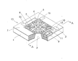
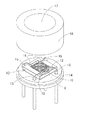
以下、図面に従って本発明の実施例について説明する。図1は本発明のサーモパイル素子の構造を示す一部破断拡大斜視図であり、図2は図1のA−A線で切断した断面図である。図3は本発明のサーモパイル素子を用いた赤外線センサの展開斜視図である。 Embodiments of the present invention will be described below with reference to the drawings. FIG. 1 is a partially broken enlarged perspective view showing the structure of the thermopile element of the present invention, and FIG. 2 is a cross-sectional view taken along the line AA of FIG. FIG. 3 is a developed perspective view of an infrared sensor using the thermopile element of the present invention.
図1および図2において、シリコン基板1の一面に二酸化ケイ素または窒化ケイ素等の絶縁膜3が設けられ、基板1の裏面側から異方性エッチングによって空洞部2が形成されている。空洞部2上には絶縁膜3からなるメンブレン4を形成している。さらに前記メンブレン4上には異種金属からなる熱電対の温接点部5が、そしてメンブレン周辺のヒートシンク部7には冷接点部6が配置されて、これら熱電対は複数個直列に接続された熱電対列を形成している。また熱電対列の温接点部5には黒体等の赤外線吸収体8が載置されている。ヒートシンク部7には、薄膜サーミスタ素子10が収納できる大きさの凹部9が形成され、薄膜サーミスタ素子10をこの凹部9に収納固定した後、薄膜サーミスタ素子10の電極部11とヒートシンク部7に設けられた引出用パッド部12とをワイヤーボンディング等の接続手段によって接合する。薄膜サーミスタ素子10の大きさは、長さ0.4mm×幅0.1mm×厚み0.05mmでサーミスタ薄膜は金属酸化物のターゲットを用いたスパッタリング法を用いて形成される。このようにして構成されたサーモパイル素子13は、図3に示すように、ステム14の中央部にサーモパイル素子13を載置し、サーモパイル素子13の出力端子16および薄膜サーミスタ素子10の電極部とワイヤーボンディングされた引出用パッド部12とをステム14上に設けたピン端子15にワイヤーで接続される。そしてこのサーモパイル素子13を覆うように、赤外線を選択的に透過させるための窓材17が設けられたキャンケース18をステム14に溶接して密封し赤外線センサが完成する。またサーモパイル素子は、上記実施例の他に、空洞部を有したアルミナなどの絶縁基板に、熱電対列を形成した絶縁膜を貼着してメンブレンを形成し、メンブレン周辺のヒートシンク部にチップサーミスタが収納できる大きさの凹部を形成してチップサーミスタ素子を収納固定し、チップサーミスタの電極とヒートシンク部に設けた引出用パッド部とをワイヤーボンディング等の手段によって接合して作製してもよい。
1 and 2, an
完成した赤外線センサは、被測定体から発せられる赤外線をサーモパイル素子の赤外線吸収体で受光することによってメンブレンの温度が上昇し、サーモパイル素子の温接点部と冷接点部との間に温度差が生じる。この温度差によって生じる起電力をサーモパイル素子の出力電圧としてサーモパイル素子の出力端子から取り出す。同時に冷接点部の温度を基板のヒートシンク部に形成した凹部内に収納固定した薄膜サーミスタ素子によって抵抗値の変化として素早く検知して、入射した赤外線量を正確に測定して被測定体の温度を正確に測ることができる。 In the completed infrared sensor, the temperature of the membrane rises by receiving infrared rays emitted from the object to be measured by the infrared absorber of the thermopile element, and a temperature difference is generated between the hot junction part and the cold junction part of the thermopile element. . The electromotive force generated by this temperature difference is taken out from the output terminal of the thermopile element as the output voltage of the thermopile element. At the same time, the temperature of the cold junction part is quickly detected as a change in resistance value by a thin film thermistor element housed and fixed in a recess formed in the heat sink part of the substrate, and the temperature of the object to be measured is measured accurately by measuring the amount of incident infrared rays. It can be measured accurately.
1 シリコン基板
3 絶縁膜
4 メンブレン
5 温接点部
6 冷接点部
7 ヒートシンク部
9 凹部
10 薄膜サーミスタ素子
11 電極部
12 引出用パッド部
13 サーモパイル素子
14 ステム
15 ピン端子
16 出力端子
17 窓材
18 キャンケース
DESCRIPTION OF SYMBOLS 1
Claims (3)
The thermopile element is mounted on a stem, and an output terminal of the thermocouple row constituting the thermopile element and an extraction pad portion to which the thin film thermistor element is connected are electrically connected to a pin terminal provided on the stem. The infrared sensor using the thermopile element according to claim 1 or 2, wherein the can case provided with a window material that selectively transmits infrared rays and the stem are sealed.
Priority Applications (3)
| Application Number | Priority Date | Filing Date | Title |
|---|---|---|---|
| JP2004289696A JP2006105651A (en) | 2004-10-01 | 2004-10-01 | Thermopile element and infrared sensor using it |
| US11/234,901 US20070227575A1 (en) | 2004-10-01 | 2005-09-26 | Thermopile element and infrared sensor by using the same |
| DE102005047164A DE102005047164B4 (en) | 2004-10-01 | 2005-09-30 | Thermopile element and the same infrared sensor used |
Applications Claiming Priority (1)
| Application Number | Priority Date | Filing Date | Title |
|---|---|---|---|
| JP2004289696A JP2006105651A (en) | 2004-10-01 | 2004-10-01 | Thermopile element and infrared sensor using it |
Publications (1)
| Publication Number | Publication Date |
|---|---|
| JP2006105651A true JP2006105651A (en) | 2006-04-20 |
Family
ID=36120774
Family Applications (1)
| Application Number | Title | Priority Date | Filing Date |
|---|---|---|---|
| JP2004289696A Pending JP2006105651A (en) | 2004-10-01 | 2004-10-01 | Thermopile element and infrared sensor using it |
Country Status (3)
| Country | Link |
|---|---|
| US (1) | US20070227575A1 (en) |
| JP (1) | JP2006105651A (en) |
| DE (1) | DE102005047164B4 (en) |
Cited By (3)
| Publication number | Priority date | Publication date | Assignee | Title |
|---|---|---|---|---|
| WO2011136203A1 (en) * | 2010-04-26 | 2011-11-03 | 株式会社エッチ.エム.イー. | Temperature sensor device and radiation thermometer using same, method for producing temperature sensor device, multilayered thin film thermopile using photoresist film and radiation thermometer using same, and method for producing multilayered thin film thermopile |
| JP2020505587A (en) * | 2017-01-11 | 2020-02-20 | コーニンクレッカ フィリップス エヌ ヴェKoninklijke Philips N.V. | Temperature sensor integrated on lead selenide plate detector assembly |
| WO2023248575A1 (en) * | 2022-06-24 | 2023-12-28 | 浜松ホトニクス株式会社 | Infrared detector |
Families Citing this family (7)
| Publication number | Priority date | Publication date | Assignee | Title |
|---|---|---|---|---|
| US7785002B2 (en) * | 2006-12-05 | 2010-08-31 | Delphi Technologies, Inc. | P-N junction based thermal detector |
| WO2010064650A1 (en) * | 2008-12-02 | 2010-06-10 | 株式会社村田製作所 | Gas sensor |
| DE102011056610A1 (en) * | 2011-12-19 | 2013-06-20 | Pyreos Ltd. | Infrared light sensor chip with high accuracy and method of manufacturing the infrared light sensor chip |
| GB2521476A (en) * | 2013-12-22 | 2015-06-24 | Melexis Technologies Nv | Infrared thermal sensor with good SNR |
| GB2521474A (en) * | 2013-12-22 | 2015-06-24 | Melexis Technologies Nv | Infrared thermal sensor with beams having different widths |
| GB2551397B (en) * | 2016-06-17 | 2020-03-25 | X Fab Semiconductor Foundries Gmbh | Thermopile Test Structure And Methods Employing Same |
| CN107560736A (en) * | 2017-09-20 | 2018-01-09 | 深圳市美思先端电子有限公司 | A kind of thermopile IR temperature sensor applied to electromagnetic oven and preparation method thereof |
Citations (3)
| Publication number | Priority date | Publication date | Assignee | Title |
|---|---|---|---|---|
| JPH106543A (en) * | 1996-06-26 | 1998-01-13 | Kyocera Corp | Thermal head |
| JPH11258055A (en) * | 1998-03-12 | 1999-09-24 | Omron Corp | Thermopile type temperature sensor |
| JP2003065854A (en) * | 2001-08-24 | 2003-03-05 | Murata Mfg Co Ltd | Thermopile device and electronic device using it |
Family Cites Families (5)
| Publication number | Priority date | Publication date | Assignee | Title |
|---|---|---|---|---|
| JP3258066B2 (en) * | 1991-03-05 | 2002-02-18 | シチズン時計株式会社 | Manufacturing method of thermopile type infrared sensor |
| EP1039280B1 (en) * | 1999-03-24 | 2010-05-12 | Ishizuka Electronics Corp. | Thermopile-type infrared sensor and process for producing the same |
| JP2001349787A (en) * | 2000-06-06 | 2001-12-21 | Seiko Epson Corp | Infrared detecting element and thermometer |
| US7061080B2 (en) * | 2001-06-11 | 2006-06-13 | Fairchild Korea Semiconductor Ltd. | Power module package having improved heat dissipating capability |
| US6828171B2 (en) * | 2002-01-16 | 2004-12-07 | Xerox Corporation | Systems and methods for thermal isolation of a silicon structure |
-
2004
- 2004-10-01 JP JP2004289696A patent/JP2006105651A/en active Pending
-
2005
- 2005-09-26 US US11/234,901 patent/US20070227575A1/en not_active Abandoned
- 2005-09-30 DE DE102005047164A patent/DE102005047164B4/en not_active Expired - Fee Related
Patent Citations (3)
| Publication number | Priority date | Publication date | Assignee | Title |
|---|---|---|---|---|
| JPH106543A (en) * | 1996-06-26 | 1998-01-13 | Kyocera Corp | Thermal head |
| JPH11258055A (en) * | 1998-03-12 | 1999-09-24 | Omron Corp | Thermopile type temperature sensor |
| JP2003065854A (en) * | 2001-08-24 | 2003-03-05 | Murata Mfg Co Ltd | Thermopile device and electronic device using it |
Cited By (5)
| Publication number | Priority date | Publication date | Assignee | Title |
|---|---|---|---|---|
| WO2011136203A1 (en) * | 2010-04-26 | 2011-11-03 | 株式会社エッチ.エム.イー. | Temperature sensor device and radiation thermometer using same, method for producing temperature sensor device, multilayered thin film thermopile using photoresist film and radiation thermometer using same, and method for producing multilayered thin film thermopile |
| JP2015227880A (en) * | 2010-04-26 | 2015-12-17 | 株式会社エッチ.エム.イー | Temperature sensor element and radiation thermometer using the same, method for manufacturing temperature sensor element, multilayer thin film thermopile using photoresist film, radiation thermometer using the thermopile, and method for manufacturing multilayer thin film thermopile |
| US9759613B2 (en) | 2010-04-26 | 2017-09-12 | Hme Co., Ltd. | Temperature sensor device and radiation thermometer using this device, production method of temperature sensor device, multi-layered thin film thermopile using photo-resist film and radiation thermometer using this thermopile, and production method of multi-layered thin film thermopile |
| JP2020505587A (en) * | 2017-01-11 | 2020-02-20 | コーニンクレッカ フィリップス エヌ ヴェKoninklijke Philips N.V. | Temperature sensor integrated on lead selenide plate detector assembly |
| WO2023248575A1 (en) * | 2022-06-24 | 2023-12-28 | 浜松ホトニクス株式会社 | Infrared detector |
Also Published As
| Publication number | Publication date |
|---|---|
| US20070227575A1 (en) | 2007-10-04 |
| DE102005047164B4 (en) | 2011-03-10 |
| DE102005047164A1 (en) | 2006-04-20 |
Similar Documents
| Publication | Publication Date | Title |
|---|---|---|
| US5054936A (en) | Sensor for active thermal detection | |
| TWI621837B (en) | Method and system for measuring heat flux | |
| US7752909B2 (en) | Flow sensor with non-contact temperature detecting means | |
| US6300554B1 (en) | Method of fabricating thermoelectric sensor and thermoelectric sensor device | |
| US20070227575A1 (en) | Thermopile element and infrared sensor by using the same | |
| KR100539205B1 (en) | Measuring tip for a radiation thermometer | |
| JP2008145133A (en) | Radiation thermometer | |
| US10175120B2 (en) | Internal temperature measurement method and internal temperature measurement device | |
| KR101745985B1 (en) | Catalytic combustion type gas sensor | |
| JP2002071452A (en) | Thermal infrared detector | |
| CN105745518A (en) | Internal temperature sensor | |
| JP5530274B2 (en) | Temperature sensor | |
| JP5001007B2 (en) | Infrared sensor utilizing optimized surface | |
| US8215831B2 (en) | Sensor element | |
| JP5564681B2 (en) | Infrared sensor | |
| JP2011203226A (en) | Infrared sensor module | |
| US20200232853A1 (en) | Non-contact type infrared temperature sensor module | |
| JP2000131147A (en) | Infrared sensor | |
| JP2002156283A (en) | Thermopile-type infrared sensor | |
| JP2003294526A (en) | Laser power detection device | |
| JPH04299225A (en) | Clinical thermometer | |
| JP2014048138A (en) | Multilayer thin film thermopile using photosensitive dry film resist, radiation thermometer using the same and method for manufacturing the multilayer thin film thermopile | |
| CN218628663U (en) | Thermopile infrared sensor and thermal shock resistant non-contact temperature measurement gun | |
| JP3855458B2 (en) | Radiation temperature detector | |
| JP6820789B2 (en) | Infrared sensor device |
Legal Events
| Date | Code | Title | Description |
|---|---|---|---|
| A621 | Written request for application examination |
Free format text: JAPANESE INTERMEDIATE CODE: A621 Effective date: 20070919 |
|
| A977 | Report on retrieval |
Free format text: JAPANESE INTERMEDIATE CODE: A971007 Effective date: 20091022 |
|
| A131 | Notification of reasons for refusal |
Free format text: JAPANESE INTERMEDIATE CODE: A131 Effective date: 20100112 |
|
| A521 | Request for written amendment filed |
Free format text: JAPANESE INTERMEDIATE CODE: A523 Effective date: 20100128 |
|
| A131 | Notification of reasons for refusal |
Free format text: JAPANESE INTERMEDIATE CODE: A131 Effective date: 20100608 |
|
| A02 | Decision of refusal |
Free format text: JAPANESE INTERMEDIATE CODE: A02 Effective date: 20110419 |