JP2005519456A - Formation of self-aligned pattern using two wavelengths - Google Patents
Formation of self-aligned pattern using two wavelengths Download PDFInfo
- Publication number
- JP2005519456A JP2005519456A JP2003571795A JP2003571795A JP2005519456A JP 2005519456 A JP2005519456 A JP 2005519456A JP 2003571795 A JP2003571795 A JP 2003571795A JP 2003571795 A JP2003571795 A JP 2003571795A JP 2005519456 A JP2005519456 A JP 2005519456A
- Authority
- JP
- Japan
- Prior art keywords
- radiation
- wavelength
- lithography
- layer
- photoresist
- Prior art date
- Legal status (The legal status is an assumption and is not a legal conclusion. Google has not performed a legal analysis and makes no representation as to the accuracy of the status listed.)
- Pending
Links
Images


Classifications
-
- G—PHYSICS
- G03—PHOTOGRAPHY; CINEMATOGRAPHY; ANALOGOUS TECHNIQUES USING WAVES OTHER THAN OPTICAL WAVES; ELECTROGRAPHY; HOLOGRAPHY
- G03F—PHOTOMECHANICAL PRODUCTION OF TEXTURED OR PATTERNED SURFACES, e.g. FOR PRINTING, FOR PROCESSING OF SEMICONDUCTOR DEVICES; MATERIALS THEREFOR; ORIGINALS THEREFOR; APPARATUS SPECIALLY ADAPTED THEREFOR
- G03F7/00—Photomechanical, e.g. photolithographic, production of textured or patterned surfaces, e.g. printing surfaces; Materials therefor, e.g. comprising photoresists; Apparatus specially adapted therefor
- G03F7/70—Microphotolithographic exposure; Apparatus therefor
- G03F7/70425—Imaging strategies, e.g. for increasing throughput or resolution, printing product fields larger than the image field or compensating lithography- or non-lithography errors, e.g. proximity correction, mix-and-match, stitching or double patterning
- G03F7/7045—Hybrid exposures, i.e. multiple exposures of the same area using different types of exposure apparatus, e.g. combining projection, proximity, direct write, interferometric, UV, x-ray or particle beam
-
- G—PHYSICS
- G03—PHOTOGRAPHY; CINEMATOGRAPHY; ANALOGOUS TECHNIQUES USING WAVES OTHER THAN OPTICAL WAVES; ELECTROGRAPHY; HOLOGRAPHY
- G03F—PHOTOMECHANICAL PRODUCTION OF TEXTURED OR PATTERNED SURFACES, e.g. FOR PRINTING, FOR PROCESSING OF SEMICONDUCTOR DEVICES; MATERIALS THEREFOR; ORIGINALS THEREFOR; APPARATUS SPECIALLY ADAPTED THEREFOR
- G03F7/00—Photomechanical, e.g. photolithographic, production of textured or patterned surfaces, e.g. printing surfaces; Materials therefor, e.g. comprising photoresists; Apparatus specially adapted therefor
- G03F7/004—Photosensitive materials
- G03F7/075—Silicon-containing compounds
- G03F7/0757—Macromolecular compounds containing Si-O, Si-C or Si-N bonds
-
- G—PHYSICS
- G03—PHOTOGRAPHY; CINEMATOGRAPHY; ANALOGOUS TECHNIQUES USING WAVES OTHER THAN OPTICAL WAVES; ELECTROGRAPHY; HOLOGRAPHY
- G03F—PHOTOMECHANICAL PRODUCTION OF TEXTURED OR PATTERNED SURFACES, e.g. FOR PRINTING, FOR PROCESSING OF SEMICONDUCTOR DEVICES; MATERIALS THEREFOR; ORIGINALS THEREFOR; APPARATUS SPECIALLY ADAPTED THEREFOR
- G03F7/00—Photomechanical, e.g. photolithographic, production of textured or patterned surfaces, e.g. printing surfaces; Materials therefor, e.g. comprising photoresists; Apparatus specially adapted therefor
- G03F7/004—Photosensitive materials
- G03F7/09—Photosensitive materials characterised by structural details, e.g. supports, auxiliary layers
- G03F7/095—Photosensitive materials characterised by structural details, e.g. supports, auxiliary layers having more than one photosensitive layer
-
- G—PHYSICS
- G03—PHOTOGRAPHY; CINEMATOGRAPHY; ANALOGOUS TECHNIQUES USING WAVES OTHER THAN OPTICAL WAVES; ELECTROGRAPHY; HOLOGRAPHY
- G03F—PHOTOMECHANICAL PRODUCTION OF TEXTURED OR PATTERNED SURFACES, e.g. FOR PRINTING, FOR PROCESSING OF SEMICONDUCTOR DEVICES; MATERIALS THEREFOR; ORIGINALS THEREFOR; APPARATUS SPECIALLY ADAPTED THEREFOR
- G03F7/00—Photomechanical, e.g. photolithographic, production of textured or patterned surfaces, e.g. printing surfaces; Materials therefor, e.g. comprising photoresists; Apparatus specially adapted therefor
- G03F7/20—Exposure; Apparatus therefor
- G03F7/2022—Multi-step exposure, e.g. hybrid; backside exposure; blanket exposure, e.g. for image reversal; edge exposure, e.g. for edge bead removal; corrective exposure
-
- H—ELECTRICITY
- H01—ELECTRIC ELEMENTS
- H01L—SEMICONDUCTOR DEVICES NOT COVERED BY CLASS H10
- H01L21/00—Processes or apparatus adapted for the manufacture or treatment of semiconductor or solid state devices or of parts thereof
- H01L21/02—Manufacture or treatment of semiconductor devices or of parts thereof
- H01L21/027—Making masks on semiconductor bodies for further photolithographic processing not provided for in group H01L21/18 or H01L21/34
- H01L21/0271—Making masks on semiconductor bodies for further photolithographic processing not provided for in group H01L21/18 or H01L21/34 comprising organic layers
- H01L21/0273—Making masks on semiconductor bodies for further photolithographic processing not provided for in group H01L21/18 or H01L21/34 comprising organic layers characterised by the treatment of photoresist layers
- H01L21/0274—Photolithographic processes
Landscapes
- Physics & Mathematics (AREA)
- General Physics & Mathematics (AREA)
- Engineering & Computer Science (AREA)
- Architecture (AREA)
- Structural Engineering (AREA)
- Spectroscopy & Molecular Physics (AREA)
- Condensed Matter Physics & Semiconductors (AREA)
- Manufacturing & Machinery (AREA)
- Computer Hardware Design (AREA)
- Microelectronics & Electronic Packaging (AREA)
- Power Engineering (AREA)
- Exposure And Positioning Against Photoresist Photosensitive Materials (AREA)
- Photosensitive Polymer And Photoresist Processing (AREA)
- Exposure Of Semiconductors, Excluding Electron Or Ion Beam Exposure (AREA)
Abstract
リソグラフィで達成可能な寸法以下のフィーチャをパターニングするための集積回路の製造プロセスをここに開示する。このプロセスは、基板に形成された従来の親油性のフォトレジスト層の表面に被覆した、光塩基発生剤および触媒量の水を含むアリールアルコキシシランの膜を第1および第2のリソグラフィ波長の放射に順にさらすステップを有する。第1のリソグラフィ波長は、第2のリソグラフィ波長より短い。第1のリソグラフィ波長への露光により、フォトレジスト層内に自己整合マスクが形成される。Disclosed herein is an integrated circuit fabrication process for patterning sub-dimensional features that can be achieved with lithography. This process involves the application of a film of an arylalkoxysilane containing a photobase generator and a catalytic amount of water coated on the surface of a conventional lipophilic photoresist layer formed on a substrate to emit radiation at first and second lithography wavelengths. In turn. The first lithography wavelength is shorter than the second lithography wavelength. Exposure to the first lithography wavelength forms a self-aligned mask in the photoresist layer.
Description
本発明は、一般に自己整合パターンの形成に関する。本発明は、より詳細には、従来の紫外線(UV)リソグラフィによって達成可能な解像度よりも高い解像度を実現する、二波長を使用した自己整合パターンの形成に関する。 The present invention generally relates to the formation of self-aligned patterns. The present invention relates more particularly to the formation of self-aligned patterns using dual wavelengths that achieve a higher resolution than can be achieved by conventional ultraviolet (UV) lithography.
半導体すなわちIC産業では、高機能化と製造コストの削減を達成するために、より小さいチップ面積に、より高い集積度でデバイスを集積させた集積回路(IC)を製造することを目指している。この大規模集積化に伴い、回路寸法およびデバイスのフィーチャ(feature)が微細化し続けている。電界効果トランジスタのゲート長や導電ラインの幅など、構造の寸法を微細化できる能力はリソグラフィの性能によって牽引されている。 The semiconductor or IC industry aims to manufacture integrated circuits (ICs) in which devices are integrated with a higher degree of integration in a smaller chip area in order to achieve higher functionality and reduced manufacturing costs. With this large scale integration, circuit dimensions and device features continue to shrink. The ability to miniaturize the structure dimensions, such as the gate length of a field effect transistor and the width of a conductive line, is driven by lithography performance.
半導体の製造技術においては、フォトマスク(マスクとも呼ばれることがある)またはレチクルを使用することが多い。放射が照射され、マスクまたはレチクルを透過するかこれらに反射して、半導体ウェハ上に像が形成される。通常、ウェハに像を結像させて、材料(例えばフォトレジスト材)の層がパターニングされる。このフォトレジスト材は、今度は、ドーピング領域、成膜領域、エッチング領域、または集積回路(IC)に関連するその他の構造を画定するために使用される。また、このフォトレジスト材が、集積回路の金属層に関連する導電ラインまたは導電パッドを画定することもある。さらに、フォトレジスト材が、分離領域、トランジスタのゲート、またはトランジスタのその他の構造または構成要素を画定することもある。 In semiconductor manufacturing technology, a photomask (sometimes called a mask) or a reticle is often used. Radiation is emitted and passes through or reflects off the mask or reticle to form an image on the semiconductor wafer. Usually, an image is formed on a wafer and a layer of material (eg, a photoresist material) is patterned. This photoresist material is in turn used to define doping regions, deposition regions, etching regions, or other structures associated with integrated circuits (ICs). The photoresist material may also define conductive lines or pads associated with the metal layers of the integrated circuit. Further, the photoresist material may define isolation regions, transistor gates, or other structures or components of the transistor.
従来のリソグラフィ・システムは、一般に、フォトレジスト材に像またはパターンを転写するために1以上の波長の電磁放射または光を照射するように構成された光源を備えている。この光源は、365ナノメートル(nm)、248nmおよび/または193nmの波長の放射を発生させ得る。この放射によってパターニングされるフォトレジスト材には、この放射の波長に感受性を有するものが選択される。好ましくは、放射が照射されたフォトレジスト材の領域は、後続の現像プロセス工程において当該領域が適切に可溶化または不溶化するような光化学反応を受ける。 Conventional lithography systems generally include a light source configured to irradiate one or more wavelengths of electromagnetic radiation or light to transfer an image or pattern to a photoresist material. The light source may generate radiation at a wavelength of 365 nanometers (nm), 248 nm and / or 193 nm. The photoresist material that is patterned by this radiation is selected to be sensitive to the wavelength of this radiation. Preferably, the areas of the photoresist material that have been irradiated are subjected to a photochemical reaction that will appropriately solubilize or insolubilize the areas in subsequent development process steps.
フィーチャの解像度は、部分的には露光波長(exposure wavelength)に比例するため、短い露光波長(例えば157nm、126nmまたは13.4nm)を使用してフォトレジスト材をパターニングすることが望ましい。しかし、このような短波長で半導体集積デバイスを再現性よく製造できる材料またはプロセスは、仮に存在したとしてもほとんどない。365nm、248nmまたは193nmリソグラフィ・システムに使用される有機系のフォトレジスト材などの、従来のフォトレジスト材を使用しようという試みには問題がないわけではない。有機系のフォトレジスト材は、短いリソグラフィ波長すなわち露光波長で単層をパターニングする用途では、単位厚さあたりの光の吸収が大きい。このため、従来の有機系のフォトレジスト材では露光用の放射に対する透過度が次第に低下していき、フォトレジスト材の厚さ全体にわたって必要な光化学反応が生じなくなる。 Because feature resolution is partially proportional to the exposure wavelength, it is desirable to pattern photoresist materials using short exposure wavelengths (eg, 157 nm, 126 nm, or 13.4 nm). However, there are few, if any, materials or processes that can manufacture semiconductor integrated devices with such short wavelengths with good reproducibility. Attempts to use conventional photoresist materials, such as organic photoresist materials used in 365 nm, 248 nm or 193 nm lithography systems are not without problems. Organic photoresist materials absorb a large amount of light per unit thickness in applications where a single layer is patterned at a short lithography wavelength, that is, an exposure wavelength. For this reason, in the conventional organic photoresist material, the transmittance with respect to the radiation for exposure gradually decreases, and the necessary photochemical reaction does not occur over the entire thickness of the photoresist material.
この欠点を克服するために、従来のフォトレジスト材の層を(長波長リソグラフィの場合と比べて)薄くして短波長リソグラフィを行う試みが行われている。しかし、フォトレジスト材の膜厚を下げると、特にエッチング処理において問題となる。このほかの問題として、膜厚を下げると、パターンの忠実度(fidelity)が低下したり、薄膜が不安定となったり、十分な結像性能が得られなくなったりする。 In order to overcome this drawback, attempts have been made to perform short wavelength lithography with a thin layer of conventional photoresist material (as compared to long wavelength lithography). However, if the film thickness of the photoresist material is lowered, it becomes a problem particularly in the etching process. As other problems, when the film thickness is lowered, the fidelity of the pattern is lowered, the thin film becomes unstable, and sufficient imaging performance cannot be obtained.
このように、従来のフォトレジスト材の使用を、深紫外線(DUV)または極紫外線(EUV)の範囲の短リソグラフィ波長に効率的に拡張させるためのシステムならびに方法が求められている。また、従来のリソグラフィの技術、材料または装置を大きく変更せずに、短リソグラフィ波長のフィーチャ解像度を達成するパターン形成のためのシステムならびに方法も求められている。さらに、パターンの自己整合を提供して、マスクの重ね合わせを不要にするプロセスまたは方法も求められている。 Thus, there is a need for systems and methods for efficiently extending the use of conventional photoresist materials to short lithography wavelengths in the deep ultraviolet (DUV) or extreme ultraviolet (EUV) range. There is also a need for systems and methods for patterning that achieve feature resolution at short lithographic wavelengths without significant changes in conventional lithographic techniques, materials or equipment. There is a further need for a process or method that provides pattern self-alignment and eliminates mask overlay.
代表的な一実施形態は、集積回路の製造プロセスに関する。このプロセスは、基板に設けたフォトレジスト材を第1のリソグラフィ波長の第1の放射にさらす(露光させる)ステップと、マスクまたはレチクル上に設けられたパターンに従ってフォトレジスト材の上部を選択的に変化させるステップと、を含む。このプロセスは、フォトレジスト材を第2のリソグラフィ波長の第2の放射にさらすステップをさらに含む。第1のリソグラフィ波長は第2のリソグラフィ波長より短い。フォトレジスト材の変化を受けた上部は第2の放射を透過させない。 One exemplary embodiment relates to an integrated circuit manufacturing process. The process includes exposing (exposing) a photoresist material provided on a substrate to a first radiation of a first lithography wavelength and selectively overlying the top of the photoresist material according to a pattern provided on a mask or reticle. Changing. The process further includes exposing the photoresist material to a second radiation at a second lithography wavelength. The first lithography wavelength is shorter than the second lithography wavelength. The upper part subjected to the change of the photoresist material does not transmit the second radiation.
別の代表的な実施形態は、集積回路の製造システムに関する。このシステムは、第1のリソグラフィ波長の第1の放射を提供する第1の光源と、第2のリソグラフィ波長の第2の放射を提供する第2の光源と、を備える。このシステムは、フォトレジスト層に設けた自己整合マスクをさらに含む。この自己整合マスクは、パターニングされたマスクまたはレチクルに従って第1のリソグラフィ波長の第1の放射に露光させて形成されている。 Another exemplary embodiment relates to an integrated circuit manufacturing system. The system comprises a first light source that provides a first radiation at a first lithographic wavelength and a second light source that provides a second radiation at a second lithographic wavelength. The system further includes a self-aligned mask provided on the photoresist layer. The self-aligned mask is formed by exposure to a first radiation of a first lithography wavelength according to a patterned mask or reticle.
さらに別の代表的な実施形態は、現在入手可能なDUV−248nmおよびDUV−193nmのフォトレジストの使用を、157nm、127nmおよび13.4nmのリソグラフィ手法(regimen)に拡張させる方法に関する。この方法は、短リソグラフィ波長の第1の放射を提供するステップを含む。この方法は、マスクまたはレチクル上に設けられたパターンに従って、基板に設けたフォトレジスト層の上部を変化させるステップをさらに含む。フォトレジスト層の変化を受けた上部は、第1の放射を受けた少なくとも1つの重合部を有する。変化を受けた上部は、マスクまたはレチクルのパターンを含む。 Yet another exemplary embodiment relates to a method that extends the use of currently available DUV-248 nm and DUV-193 nm photoresists to 157 nm, 127 nm, and 13.4 nm lithography. The method includes providing a first radiation at a short lithographic wavelength. The method further includes changing the top of the photoresist layer provided on the substrate according to a pattern provided on the mask or reticle. The top of the photoresist layer that has undergone the change has at least one overlapping portion that has received the first radiation. The changed top includes a mask or reticle pattern.
添付の図面と併せて下記の詳細な説明を読めば、好ましい実施形態がより明確に理解されるであろう。添付の図面において、同一の参照符号は同一の要素を参照している。 The preferred embodiment will be more clearly understood from the following detailed description when read in conjunction with the accompanying drawings. In the accompanying drawings, the same reference signs refer to the same elements.
フォトレジスト材にパターンを自己整合させるための有利な手法の代表的な一実施形態に関して、図1〜10を参照して記載する。また、この有利な手法は、第1の波長λ1(二波長のうち短い方)の解像度限界よりも小さいオーダーの、リソグラフィによって達成可能な解像度以下のフィーチャ解像度を提供する。 One exemplary embodiment of an advantageous technique for self-aligning a pattern to a photoresist material will be described with reference to FIGS. This advantageous approach also provides feature resolution below the resolution achievable by lithography, on the order of less than the resolution limit of the first wavelength λ 1 (the shorter of the two wavelengths).
図1を参照すると、この有利なプロセスを構成する第1の露光工程(exposure process)を、集積回路(IC)の一部に実施する。この部分は、基板12上に設けたフォトレジスト層14を含む。基板12は、ICウェハ、半導性材料、絶縁性材料、導電性材料、これら材料のいずれかの上部に設けた層、または基層(ベース層)であり得る。基板12は、業界標準のシリコン・ウェハであってもよい。基板12は特に限定されない。
Referring to FIG. 1, a first exposure process that constitutes this advantageous process is performed on a portion of an integrated circuit (IC). This portion includes a
基板12は、その表面の上部または下部に、絶縁性、導電性、または半導性の層を有してもよい。この絶縁性、導電性、または半導性の層は、基板12上に堆積または成長しても、基板12上の層に成長または堆積してもよい。層14は、基板12上に直接設けられているように図示されているが、基層、中間層、反射防止コーティング層等の層の上部に設けてもよい。
The
フォトレジスト層14には、第1の光源18(図3)からの電磁放射16を受けると光化学反応を起こすようなものが選択される。フォトレジスト層14は、従来のポジ型フォトレジスト材であればどのようなものであってもよい。好ましくは、フォトレジスト層14は、適切な光酸発生剤を含有し、193nmまたは248nmの波長に感光を有する親油性重合材料であり、スピン・コーティングによって100〜500nmの厚さに基板12に塗布される。
The
第1の光源18は、任意の数の電磁放射発生源であり得る。第1の光源18は、短波長の放射16を照射する単一光源または複数の光源であり得る。好ましくは、第1の光源18は、遠紫外線(DUV)の短波長(193nm、248nm)、真空紫外線(157nm、126nm)または極紫外線(EUV)、例えば11.4nm、13.4nmの範囲の放射16を提供する。放射16の短波長λ1(短リソグラフィ波長とも呼ばれることもある)は、好ましくは、o−ニトロベンゾイルのカルバミン酸エステルおよびウレタン、o−アシルオキシム、ベンゾイン カルバミン酸エステル、オキシム−ウレタン等の光塩基発生剤(photobase generators:PBG)と触媒量の水の存在下で、下の反応式1に示すように、アリールトリエトキシシランなどの有機トリアルコキシシラン単量体を重合させることができる。なお、反応式1において、Rはアリール基を表す。

第1の光源18はF2エキシマーレーザ(157nm)、XeClレーザ、ArFエキシマーレーザ(193nm)、KrFレーザ(248nm)またはレーザ生成Xeプラズマ(13.4nm、11.4nm)または放電生成プラズマ(13.4nm、11.4nm)などのレーザ光源であっても、電子ビーム、イオンビーム、γ線などの放射であってもよい。あるいは、光源18は、アルゴンレーザなど、さまざまな波長範囲の2以上の波長を発するレーザ光源であってもよい。
The
第1の光源18からの放射16が、マスクまたはレチクル20を介して、マスクまたはレチクル20上のパターンに従ってフォトレジスト層14に照射される。マスクまたはレチクル20は、好ましくは、ガラス基板(例えば融解石英)と不透明材料(例えばクロム)とを含む従来のフォトマスクまたはレチクルである。図示されていないが、光源18とフォトレジスト層14との間に、光学系(例えば1つ以上のレンズ・アセンブリ)等の別の部品または装置を設けて、マスク20上の像をフォトレジスト層14に転写させてもよい。
一実施形態においては、親油性フォトレジスト層14の表面に、光塩基発生剤と触媒量の水とを含有するアリールアルコキシシラン単量体の膜15(図2)を塗布して、この膜を短波長光λ1にさらす。必要であれば、フォトレジストの表面に、ヘキサメチルジシラザンなどの定着剤の数分子の層(few monolayers)を塗布して、アリールアルコキシシラン単量体のフォトレジストへの密着性を高めてもよい。アリールアルコキシシラン単量体の例として、フェニル−t−ブチルエーテル トリエトキシシラン、1−フェニル−t−フェニル−t−ブチルエーテル ジエトキシシランおよびベンジル−t−ブチルエーテル トリエトキシシランが挙げられる。これらの単量体は、所望の特性に応じて組み合わせるか混合してもよい。単量体は、好ましくは、Si原子と会合可能な結合を有しており、Si原子は、活性化されて、短波長での露光およびその後の現像による重合を促進することができる。単量体の光の吸収プロファイルは、好ましくは波長の関数であり、短波長側では吸光度が小さく現在の解像度の目標を達成できる一方で、より従来型に近いレジストが感受性を有する長波長側では吸光度が大きい。このような特性が好ましいものの、この特性は、特許請求の範囲に明示的に規定されていない限り、特許請求の範囲のフォトレジスト材に必ずしも必要な特性ではない。
In one embodiment, a film 15 (FIG. 2) of an arylalkoxysilane monomer containing a photobase generator and a catalytic amount of water is applied to the surface of the
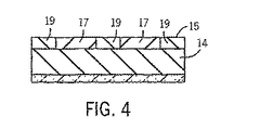
光塩基発生剤は、フォトマスク(マスク20)を通った放射に露光されると、光塩基を発生させ、この光塩基は、水の存在下で、膜15の被露光部分(図3,4)のアリールアルコキシシラン単量体の重合を触媒する。157nmでは、アリールアルコキシシラン単量体(領域19参照)はある程度の透過性を有するが、ポリ(アリールアルコキシシラン)はほぼ不透過である(領域17参照)。ポリ(アリールアルコキシシラン)(領域17)の吸光度は、157nmよりも193nmにおいて非常に高い(図10を参照)。 When exposed to radiation through a photomask (mask 20), the photobase generator generates a photobase, which in the presence of water, the exposed portion of the film 15 (FIGS. 3 and 4). ) Of the arylalkoxysilane monomer. At 157 nm, the arylalkoxysilane monomer (see region 19) has some transparency, but the poly (arylalkoxysilane) is almost impermeable (see region 17). The absorbance of poly (arylalkoxysilane) (region 17) is much higher at 193 nm than at 157 nm (see FIG. 10).
アリールアルコキシシラン/ポリ(アリールアルコキシシラン)層(領域17および領域19を含む層15)を、水/メタノール混合液で洗浄すると、非露光部分の未重合のアリールアルコキシシラン単量体(領域19)が除去されて、膜15の被露光部分のポリ(アリールアルコキシシラン)(領域17)が残る(図5)。適切な温度でベークすると、残った溶媒が除去されて、ポリ(アリールアルコキシシラン)を含む上層が残る。この上層は、後続の現像工程においてマスクとして有効に機能する。
When the arylalkoxysilane / poly (arylalkoxysilane) layer (the
自己整合マスクおよびフォトレジスト(層14および膜15)に対し、長波長λ2にてフラッド露光(flood exposing)を行うと、自己整合マスク方式に、フォトレジスト層の非マスク部分(領域21)が実効的に変化を受ける(図7)。従来技術による露光後のベーク(post-applied bake)を行い(図8)、続いてテトラメチルアンモニウム ハイドロオキサイド(TMAH)などの水性塩基中で溶媒現像を行う。フォトレジストの被露光部分を洗浄すると、フォトレジストの未露光部分23の自己整合マスク・パターンが残る(図9)。
To a self-aligned mask and photoresist (
フォトレジスト層14は、好ましくは、長い紫外(UV)波長(例えば365nm、248nmまたは193nm)放射に対し透過性を有し、短波長(例えば157nm、126nmまたは13.4nm)の放射に対しわずかな透過性を有するか半透過性を有するポジ型フォトレジストである。例えば、フォトレジスト層14は、住友化学(Sumitomo Chemical)のPAR720(登録商標)、PAR707M(登録商標)などの従来の193nmリソグラフィに使用するフォトレジストであっても、環境安定型化学増幅型フォトレジスト(ESCAP)であるシプリー(Shipley)のUV110(登録商標)などの、248nmリソグラフィで使用するフォトレジストであってもよい。
膜15およびフォトレジスト層14は、2つの別個の層を有する二層式層フォトレジストを形成している。上層(膜15)は、重合して長波長の放射を透過させなくなる。この長波長の放射は、下層(層14)が高い感受性を有するものである。下層は、より従来型に近いフォトレジスト材とすることができ、上層とは異なり、短波長の放射によって効率的にパターニングされない。
層14の重合部または重合領域17に示すように、図3の第1の露光工程後にマスク20からパターンが転写されている。重合領域17のフィーチャ解像度は、放射16の短露光波長の約1/2〜1倍である。例を挙げると、157nmの放射による露光によって形成される重合領域17のフィーチャ解像度は、約72〜157nmとなる。126nmまたは13.4nmの波長の放射16では、可能な解像度はそれぞれ約63〜126nm、または6.7〜13.4nmとなる。
As shown in the superposed portion or superposed
重合部または重合領域17は、好ましくは、フォトレジスト層14の露光に従来使用していた長リソグラフィ波長(例えば365nm、248nmまたは193nm)の放射を透過させない、すなわちこれらに非透過である。この不透過により、重合部または重合領域17が、部分10に対する長波長の露光工程(図7)において自己整合マスクまたはレチクルとして機能するようになる。
The polymerized portion or polymerized
第2の露光工程(図7)において、部分10にパターンを転写するのにマスク20(図3)は不要である。マスク20に代わり、膜15の重合部または重合領域17が、マスク20によって提供されるパターンまたは像を有する自己整合マスクとして有利に機能する。第2の光源28は、長リソグラフィ波長または長露光波長(例えば248nm)の放射30によるフラッド露光を提供する。放射30の波長と層14とは、層14の被露光領域(すなわち重合部または重合領域17によって覆われていない部分)が放射30を透過させ、光化学反応を受けて可溶化する(図8の可溶部または可溶領域21)一方で、重合部または重合領域17の下の部分は、重合部または重合領域17が放射を透過させないため放射30に露光されず、不溶性のままとなる(図8の不溶部または不溶領域23)ように選択される。
In the second exposure step (FIG. 7), the mask 20 (FIG. 3) is not required to transfer the pattern to the
第1の光源18および第2の光源28は、同じ光源で、二波長、すなわち短波長と長波長のUVリソグラフィ波長の放射を発生させるものであってもよい。あるいは、光源28はエキシマ・レーザ、ND:YAGレーザ、周波数逓倍ND:YAGレーザ、He−Ne走査レーザなどであってもよい。光源28と部分10との間に追加の部品または装置を設けて、層14に所望の放射30を照射してもよい。
The
したがって、第2の露光工程ののち、マスク20に設けられたパターンまたは像が、第1の露光工程によって決定される解像度にてフォトレジスト層14に完全に転写される。層14の被露光部は、可溶部または可溶領域21となり、層14の非露光部または非露光領域23は、(重合部または重合領域17によって)不溶性の部分となる(図8,9参照)。現像工程において、層14の可溶部または可溶領域17が除去され、架橋部すなわち架橋領域17と、層14の不溶部または不溶領域21のみが基板12に残る(図9)。好ましくは、現像工程で、層14を含む材料を現像するために従来技術に用いた溶媒現像液を使用する。例えば、248nmリソグラフィに使用するフォトレジストの場合、0.24Nテトラメチルアンモニウム ハイドロオキサイド現像液を使用して、可溶部または可溶領域21を除去することができる。
Therefore, after the second exposure step, the pattern or image provided on the
好ましい実施形態においては、重合部または重合領域17は、短リソグラフィ波長の放射に露光されて不溶化する。あるいは、重合部または重合領域17は、マスクとして機能すれば、第2の露光工程において長リソグラフィ波長の放射に露光されて、さらに化学変化を受けてもよい。重合部または重合領域17は、好ましくは、現像工程後も残り、エッチング工程または成膜工程などの部分10に対する後続の処理工程を支援する。領域17は、プラズマ・エッチング条件下で二酸化シリコン(SiO2)に転換され得るため、異方性エッチングにおいて、フォトレジスト層に対する上層のエッチングの安定性を改善させることができる。
In a preferred embodiment, the overlap or overlap
このように、従来の装置および材料を使用して高いフィーチャ解像度を達成するための有利な手法についてここに記載した。異なる波長の放射を順番に使用する(短リソグラフィ波長の後に長リソグラフィ波長を使用する)ことによって、従来の長波長リソグラフィ用のフォトレジストを、短リソグラフィ波長の放射によってパターニングすることができる。また、パターン解像度は、長波長リソグラフィによって達成可能なパターン解像度よりも高くなり、短リソグラフィ波長のオーダーのパターン解像度が得られる。さらに、パターニング・プロセスで形成した自己整合マスクを使用することによって、マスクの重ね合わせまたはアラインメント上の問題点を回避することができる。 Thus, an advantageous approach for achieving high feature resolution using conventional equipment and materials has been described herein. By using different wavelengths of radiation in sequence (using a short lithography wavelength followed by a long lithography wavelength), a conventional long wavelength lithography photoresist can be patterned with short lithography wavelength radiation. Also, the pattern resolution is higher than the pattern resolution achievable by long wavelength lithography, and a pattern resolution on the order of short lithography wavelengths is obtained. Further, by using a self-aligned mask formed by a patterning process, mask overlay or alignment problems can be avoided.
図10に、各種アリールシロキサン材料の吸収体と波長との関係を示す。ライン102は、X軸108(波長λ1)に対するY軸110の吸光度(1/μm)を示す。ライン102は、同様にポリ(1−フェニル−1−フェニル−t−ブチルエーテル シロキサン)の吸光度を、ライン104はポリ(フェニル−t−ブチルエーテル シロキサン)の吸光度を、ライン106は同様にポリ(ベンジル−t−ブチルエーテル シロキサン)の吸光度を示す。157nmでの吸光度に対する193nmでの吸光度の変化すなわち差によって、優れたリソグラフィ・プロセスを有利に設計できるようになる。
FIG. 10 shows the relationship between the absorbers and wavelengths of various arylsiloxane materials. A
好ましい実施形態および具体例を挙げたが、これらは説明のみを目的としており、本明細書に記載した詳細に本発明を限定するものではないことが理解される。例えば、具体的な光の波長を挙げたが、他の波長の光を使用してもよい。特許請求の範囲から逸脱することなく、特許請求の範囲の均等物の範囲内でさまざまな変更を加えることが可能である。 While preferred embodiments and specific examples have been given, it is understood that they are for illustrative purposes only and are not intended to limit the invention to the details described herein. For example, although the specific wavelength of light is mentioned, light of other wavelengths may be used. Various changes may be made within the scope of the equivalents of the claims without departing from the scope of the claims.
Claims (10)
基板上の、アリールアルコキシシラン(15)を含有するフォトレジスト材(14)を第1のリソグラフィ波長(λ1)の第1の放射(116)にさらすステップと、
マスクまたはレチクル上に設けられたパターンに従って前記フォトレジスト材(14)の上部を選択的に変化させるステップと、
前記フォトレジスト材(14)を第2のリソグラフィ波長(λ2)の第2の放射(30)にさらすステップと、を有し、
前記第1のリソグラフィ波長(λ1)は前記第2のリソグラフィ波長(λ2)より短く、前記フォトレジスト材(14)の前記変化を受けた上部は前記第2の放射(λ2)を透過させないことを特徴とするプロセス。 An integrated circuit manufacturing process comprising:
Exposing a photoresist material (14) containing an arylalkoxysilane (15) on a substrate to a first radiation (116) of a first lithography wavelength (λ 1 );
Selectively changing the top of the photoresist material (14) according to a pattern provided on a mask or reticle;
Exposing the photoresist material (14) to a second radiation (30) of a second lithography wavelength (λ 2 );
The first lithography wavelength (λ 1 ) is shorter than the second lithography wavelength (λ 2 ), and the changed upper portion of the photoresist material (14) transmits the second radiation (λ 2 ). Process characterized by not letting it.
第1のリソグラフィ波長(λ1)の第1の放射(16)を提供する第1の光源(18)と、
第2のリソグラフィ波長(λ2)の第2の放射(30)を提供する第2の光源(28)と、
フォトレジスト層(14)に設けた自己整合マスクであって、パターニングされたマスクまたはレチクルに従って前記第1のリソグラフィ波長の前記第1の放射にさらされて形成された自己整合マスクと、を有することを特徴とするシステム。 An integrated circuit manufacturing system comprising:
A first light source (18) providing a first radiation (16) of a first lithography wavelength (λ 1 );
A second light source (28) providing a second radiation (30) of a second lithography wavelength (λ 2 );
A self-aligned mask provided in the photoresist layer (14), the self-aligned mask formed by exposure to the first radiation of the first lithography wavelength according to a patterned mask or reticle. A system characterized by
Applications Claiming Priority (2)
| Application Number | Priority Date | Filing Date | Title |
|---|---|---|---|
| US10/083,914 US6764808B2 (en) | 2002-02-27 | 2002-02-27 | Self-aligned pattern formation using wavelenghts |
| PCT/US2003/004960 WO2003073165A2 (en) | 2002-02-27 | 2003-02-21 | Self-aligned pattern formation using dual wavelengths |
Publications (2)
| Publication Number | Publication Date |
|---|---|
| JP2005519456A true JP2005519456A (en) | 2005-06-30 |
| JP2005519456A5 JP2005519456A5 (en) | 2006-04-13 |
Family
ID=27753386
Family Applications (1)
| Application Number | Title | Priority Date | Filing Date |
|---|---|---|---|
| JP2003571795A Pending JP2005519456A (en) | 2002-02-27 | 2003-02-21 | Formation of self-aligned pattern using two wavelengths |
Country Status (9)
| Country | Link |
|---|---|
| US (1) | US6764808B2 (en) |
| EP (1) | EP1478978B1 (en) |
| JP (1) | JP2005519456A (en) |
| KR (1) | KR20040094706A (en) |
| CN (1) | CN1299166C (en) |
| AU (1) | AU2003211152A1 (en) |
| DE (1) | DE60329371D1 (en) |
| TW (1) | TWI278013B (en) |
| WO (1) | WO2003073165A2 (en) |
Families Citing this family (16)
| Publication number | Priority date | Publication date | Assignee | Title |
|---|---|---|---|---|
| DE10138105A1 (en) * | 2001-08-03 | 2003-02-27 | Infineon Technologies Ag | Photoresist and method for structuring such a photoresist |
| US7501230B2 (en) * | 2002-11-04 | 2009-03-10 | Meagley Robert P | Photoactive adhesion promoter |
| DE10309266B3 (en) * | 2003-03-04 | 2005-01-13 | Infineon Technologies Ag | A method of forming an opening of a light absorbing layer on a mask |
| DE10310781A1 (en) * | 2003-03-12 | 2004-09-30 | Infineon Technologies Ag | Method for operating a microprocessor and a microprocessor arrangement |
| US7265366B2 (en) * | 2004-03-31 | 2007-09-04 | Asml Netherlands B.V. | Lithographic apparatus and device manufacturing method |
| WO2006085741A1 (en) * | 2005-02-09 | 2006-08-17 | Stichting Dutch Polymer Institute | Process for preparing a polymeric relief structure |
| US7816072B2 (en) * | 2005-05-02 | 2010-10-19 | Tokyo Ohka Kogyo Co., Ltd. | Positive resist composition and method for forming resist pattern |
| US20070166649A1 (en) * | 2006-01-18 | 2007-07-19 | Cheng-Hung Yu | Method of forming a micro device |
| CN100465666C (en) * | 2006-01-24 | 2009-03-04 | 联华电子股份有限公司 | Manufacture method of microcomponent |
| JP2007287928A (en) * | 2006-04-17 | 2007-11-01 | Nec Electronics Corp | Semiconductor integrated circuit, its manufacturing method, and mask |
| JP4660826B2 (en) * | 2006-08-18 | 2011-03-30 | 山栄化学株式会社 | Method for forming resist pattern |
| US7863150B2 (en) * | 2006-09-11 | 2011-01-04 | International Business Machines Corporation | Method to generate airgaps with a template first scheme and a self aligned blockout mask |
| KR101023077B1 (en) * | 2008-10-27 | 2011-03-24 | 주식회사 동부하이텍 | method of forming mask pattern |
| US9977339B2 (en) | 2014-01-27 | 2018-05-22 | Tokyo Electron Limited | System and method for shifting critical dimensions of patterned films |
| US9645495B2 (en) | 2014-08-13 | 2017-05-09 | Tokyo Electron Limited | Critical dimension control in photo-sensitized chemically-amplified resist |
| US11294273B2 (en) * | 2019-10-25 | 2022-04-05 | Innolux Corporation | Mask substrate and method for forming mask substrate |
Family Cites Families (10)
| Publication number | Priority date | Publication date | Assignee | Title |
|---|---|---|---|---|
| EP0098922A3 (en) | 1982-07-13 | 1986-02-12 | International Business Machines Corporation | Process for selectively generating positive and negative resist patterns from a single exposure pattern |
| US4810601A (en) * | 1984-12-07 | 1989-03-07 | International Business Machines Corporation | Top imaged resists |
| NL8500455A (en) | 1985-02-18 | 1986-09-16 | Philips Nv | METHOD FOR MANUFACTURING A SEMICONDUCTOR DEVICE, FORMING A PHOTOGRAPHIC MASK USING A TWO-LAYER PAINTING SYSTEM |
| JPH02269353A (en) | 1988-10-28 | 1990-11-02 | Hewlett Packard Co <Hp> | Method of manufacturing semiconductor by photolithography |
| US5180655A (en) * | 1988-10-28 | 1993-01-19 | Hewlett-Packard Company | Chemical compositions for improving photolithographic performance |
| JP3192879B2 (en) * | 1994-07-28 | 2001-07-30 | トヨタ自動車株式会社 | Ceramic butterfly valve and method of manufacturing the same |
| JPH09319097A (en) * | 1996-01-16 | 1997-12-12 | Sumitomo Chem Co Ltd | Method for forming resist pattern |
| JP3373147B2 (en) * | 1998-02-23 | 2003-02-04 | シャープ株式会社 | Photoresist film and pattern forming method thereof |
| FR2812450B1 (en) * | 2000-07-26 | 2003-01-10 | France Telecom | RESIN, TWO-LAYER RESIN FOR EXTREME ULTRAVIOLET (EUV) PHOTOLITHOGRAPHY AND METHOD FOR EXTREME ULTRAVIOLET (EUV) PHOTOLITHOGRAPHY |
| WO2003095026A1 (en) | 2002-05-13 | 2003-11-20 | Pflueger D Russell | Spinal disc therapy system |
-
2002
- 2002-02-27 US US10/083,914 patent/US6764808B2/en not_active Expired - Lifetime
-
2003
- 2003-02-21 WO PCT/US2003/004960 patent/WO2003073165A2/en active Application Filing
- 2003-02-21 EP EP03743156A patent/EP1478978B1/en not_active Expired - Lifetime
- 2003-02-21 CN CNB038025280A patent/CN1299166C/en not_active Expired - Fee Related
- 2003-02-21 DE DE60329371T patent/DE60329371D1/en not_active Expired - Lifetime
- 2003-02-21 AU AU2003211152A patent/AU2003211152A1/en not_active Abandoned
- 2003-02-21 JP JP2003571795A patent/JP2005519456A/en active Pending
- 2003-02-21 KR KR10-2004-7012948A patent/KR20040094706A/en active Search and Examination
- 2003-02-27 TW TW092104154A patent/TWI278013B/en not_active IP Right Cessation
Also Published As
| Publication number | Publication date |
|---|---|
| AU2003211152A1 (en) | 2003-09-09 |
| US20030162135A1 (en) | 2003-08-28 |
| TW200303573A (en) | 2003-09-01 |
| CN1299166C (en) | 2007-02-07 |
| DE60329371D1 (en) | 2009-11-05 |
| TWI278013B (en) | 2007-04-01 |
| WO2003073165A3 (en) | 2003-10-16 |
| WO2003073165A2 (en) | 2003-09-04 |
| EP1478978A2 (en) | 2004-11-24 |
| KR20040094706A (en) | 2004-11-10 |
| EP1478978B1 (en) | 2009-09-23 |
| US6764808B2 (en) | 2004-07-20 |
| CN1620634A (en) | 2005-05-25 |
Similar Documents
| Publication | Publication Date | Title |
|---|---|---|
| US7579135B2 (en) | Lithography apparatus for manufacture of integrated circuits | |
| KR100639680B1 (en) | Forming method of fine patterns for semiconductor device | |
| JP3355239B2 (en) | Pattern formation method | |
| US6966710B2 (en) | Pattern forming method and apparatus for fabricating semiconductor device | |
| JP2005519456A (en) | Formation of self-aligned pattern using two wavelengths | |
| US6767693B1 (en) | Materials and methods for sub-lithographic patterning of contact, via, and trench structures in integrated circuit devices | |
| TWI488218B (en) | Method of slimming radiation-sensitive material lines in lithographic applications | |
| JP2009534870A (en) | How to shorten the minimum pitch in a pattern | |
| KR20010015280A (en) | A method of forming a photoresist pattern | |
| US20100173247A1 (en) | Substrate planarization with imprint materials and processes | |
| US6589713B1 (en) | Process for reducing the pitch of contact holes, vias, and trench structures in integrated circuits | |
| US6602794B1 (en) | Silylation process for forming contacts | |
| CN108121160B (en) | Lithographic patterning method | |
| US6884735B1 (en) | Materials and methods for sublithographic patterning of gate structures in integrated circuit devices | |
| CN108231550B (en) | Method for manufacturing semiconductor device | |
| US6528398B1 (en) | Thinning of trench and line or contact spacing by use of dual layer photoresist | |
| KR20010037049A (en) | Lithography method using silylation | |
| KR100261162B1 (en) | Method for patterning semiconductor device | |
| US6514874B1 (en) | Method of using controlled resist footing on silicon nitride substrate for smaller spacing of integrated circuit device features | |
| Henderson et al. | Top surface imaging for extreme ultraviolet lithography | |
| JP2648004B2 (en) | Etching resistant pattern forming method | |
| US20100055624A1 (en) | Method of patterning a substrate using dual tone development | |
| US5882825A (en) | Production method of a phase shift photomask having a phase shift layer comprising SOG | |
| KR19990000089A (en) | Micro pattern formation method of semiconductor device | |
| JPH03283418A (en) | Resist pattern forming method |
Legal Events
| Date | Code | Title | Description |
|---|---|---|---|
| A521 | Request for written amendment filed |
Free format text: JAPANESE INTERMEDIATE CODE: A523 Effective date: 20060221 |
|
| A621 | Written request for application examination |
Free format text: JAPANESE INTERMEDIATE CODE: A621 Effective date: 20060221 |
|
| A131 | Notification of reasons for refusal |
Free format text: JAPANESE INTERMEDIATE CODE: A131 Effective date: 20080729 |
|
| A601 | Written request for extension of time |
Free format text: JAPANESE INTERMEDIATE CODE: A601 Effective date: 20081029 |
|
| A602 | Written permission of extension of time |
Free format text: JAPANESE INTERMEDIATE CODE: A602 Effective date: 20081106 |
|
| A601 | Written request for extension of time |
Free format text: JAPANESE INTERMEDIATE CODE: A601 Effective date: 20081201 |
|
| A602 | Written permission of extension of time |
Free format text: JAPANESE INTERMEDIATE CODE: A602 Effective date: 20081208 |
|
| A601 | Written request for extension of time |
Free format text: JAPANESE INTERMEDIATE CODE: A601 Effective date: 20081226 |
|
| A602 | Written permission of extension of time |
Free format text: JAPANESE INTERMEDIATE CODE: A602 Effective date: 20090109 |
|
| A521 | Request for written amendment filed |
Free format text: JAPANESE INTERMEDIATE CODE: A523 Effective date: 20090119 |
|
| A02 | Decision of refusal |
Free format text: JAPANESE INTERMEDIATE CODE: A02 Effective date: 20090317 |
|
| A521 | Request for written amendment filed |
Free format text: JAPANESE INTERMEDIATE CODE: A523 Effective date: 20090715 |
|
| RD03 | Notification of appointment of power of attorney |
Free format text: JAPANESE INTERMEDIATE CODE: A7423 Effective date: 20100421 |
|
| RD05 | Notification of revocation of power of attorney |
Free format text: JAPANESE INTERMEDIATE CODE: A7425 Effective date: 20100902 |