EP1478978B1 - Self-aligned pattern formation using dual wavelengths - Google Patents
Self-aligned pattern formation using dual wavelengths Download PDFInfo
- Publication number
- EP1478978B1 EP1478978B1 EP03743156A EP03743156A EP1478978B1 EP 1478978 B1 EP1478978 B1 EP 1478978B1 EP 03743156 A EP03743156 A EP 03743156A EP 03743156 A EP03743156 A EP 03743156A EP 1478978 B1 EP1478978 B1 EP 1478978B1
- Authority
- EP
- European Patent Office
- Prior art keywords
- layer
- radiation
- wavelength
- lithographic
- photoresist
- Prior art date
- Legal status (The legal status is an assumption and is not a legal conclusion. Google has not performed a legal analysis and makes no representation as to the accuracy of the status listed.)
- Expired - Lifetime
Links
- 230000007261 regionalization Effects 0.000 title description 6
- 230000009977 dual effect Effects 0.000 title description 3
- 229920002120 photoresistant polymer Polymers 0.000 claims abstract description 58
- 230000005855 radiation Effects 0.000 claims abstract description 40
- 238000000034 method Methods 0.000 claims abstract description 22
- 230000008569 process Effects 0.000 claims abstract description 16
- 239000000758 substrate Substances 0.000 claims abstract description 16
- 238000004519 manufacturing process Methods 0.000 claims abstract description 6
- 239000000463 material Substances 0.000 claims description 40
- 239000002904 solvent Substances 0.000 claims description 4
- XLYOFNOQVPJJNP-UHFFFAOYSA-N water Substances O XLYOFNOQVPJJNP-UHFFFAOYSA-N 0.000 abstract description 8
- 230000003197 catalytic effect Effects 0.000 abstract description 5
- 238000000059 patterning Methods 0.000 abstract description 3
- 239000010410 layer Substances 0.000 description 63
- 239000000178 monomer Substances 0.000 description 10
- 238000002835 absorbance Methods 0.000 description 9
- 239000010408 film Substances 0.000 description 8
- 238000001459 lithography Methods 0.000 description 7
- OKKJLVBELUTLKV-UHFFFAOYSA-N Methanol Chemical compound OC OKKJLVBELUTLKV-UHFFFAOYSA-N 0.000 description 6
- WGTYBPLFGIVFAS-UHFFFAOYSA-M tetramethylammonium hydroxide Chemical compound [OH-].C[N+](C)(C)C WGTYBPLFGIVFAS-UHFFFAOYSA-M 0.000 description 6
- VYPSYNLAJGMNEJ-UHFFFAOYSA-N Silicium dioxide Chemical compound O=[Si]=O VYPSYNLAJGMNEJ-UHFFFAOYSA-N 0.000 description 5
- 239000004065 semiconductor Substances 0.000 description 5
- 238000005530 etching Methods 0.000 description 4
- 238000012546 transfer Methods 0.000 description 4
- 230000008859 change Effects 0.000 description 3
- 230000005670 electromagnetic radiation Effects 0.000 description 3
- 238000006116 polymerization reaction Methods 0.000 description 3
- 238000012545 processing Methods 0.000 description 3
- 239000000126 substance Substances 0.000 description 3
- XKRFYHLGVUSROY-UHFFFAOYSA-N Argon Chemical compound [Ar] XKRFYHLGVUSROY-UHFFFAOYSA-N 0.000 description 2
- XUIMIQQOPSSXEZ-UHFFFAOYSA-N Silicon Chemical compound [Si] XUIMIQQOPSSXEZ-UHFFFAOYSA-N 0.000 description 2
- 238000000151 deposition Methods 0.000 description 2
- 230000008021 deposition Effects 0.000 description 2
- 238000011161 development Methods 0.000 description 2
- 230000018109 developmental process Effects 0.000 description 2
- FFUAGWLWBBFQJT-UHFFFAOYSA-N hexamethyldisilazane Chemical compound C[Si](C)(C)N[Si](C)(C)C FFUAGWLWBBFQJT-UHFFFAOYSA-N 0.000 description 2
- 239000000203 mixture Substances 0.000 description 2
- 230000003287 optical effect Effects 0.000 description 2
- 238000006552 photochemical reaction Methods 0.000 description 2
- -1 poly(phenyl-t-butylether siloxane Chemical class 0.000 description 2
- 229910052710 silicon Inorganic materials 0.000 description 2
- 239000010703 silicon Substances 0.000 description 2
- 239000000377 silicon dioxide Substances 0.000 description 2
- 235000012239 silicon dioxide Nutrition 0.000 description 2
- 238000005406 washing Methods 0.000 description 2
- UGMVAXFCZIHYHD-UHFFFAOYSA-N (2-methylpropan-2-yl)oxymethylbenzene triethoxysilane Chemical compound CCO[SiH](OCC)OCC.CC(C)(C)OCc1ccccc1 UGMVAXFCZIHYHD-UHFFFAOYSA-N 0.000 description 1
- VYZAMTAEIAYCRO-UHFFFAOYSA-N Chromium Chemical compound [Cr] VYZAMTAEIAYCRO-UHFFFAOYSA-N 0.000 description 1
- 239000006096 absorbing agent Substances 0.000 description 1
- 238000010521 absorption reaction Methods 0.000 description 1
- 238000000862 absorption spectrum Methods 0.000 description 1
- 239000002318 adhesion promoter Substances 0.000 description 1
- 239000006117 anti-reflective coating Substances 0.000 description 1
- 229910052786 argon Inorganic materials 0.000 description 1
- 125000003118 aryl group Chemical group 0.000 description 1
- 238000000429 assembly Methods 0.000 description 1
- 230000000712 assembly Effects 0.000 description 1
- IRRKWKXMRZQNDM-UHFFFAOYSA-N carbamic acid;2-hydroxy-1,2-diphenylethanone Chemical compound NC(O)=O.C=1C=CC=CC=1C(O)C(=O)C1=CC=CC=C1 IRRKWKXMRZQNDM-UHFFFAOYSA-N 0.000 description 1
- SJNSFWPIPNAYMH-UHFFFAOYSA-N carbamoyl 2-nitrobenzoate Chemical class NC(=O)OC(=O)C1=CC=CC=C1[N+]([O-])=O SJNSFWPIPNAYMH-UHFFFAOYSA-N 0.000 description 1
- 229910052804 chromium Inorganic materials 0.000 description 1
- 239000011651 chromium Substances 0.000 description 1
- 239000004020 conductor Substances 0.000 description 1
- 238000010894 electron beam technology Methods 0.000 description 1
- 230000005669 field effect Effects 0.000 description 1
- 239000005350 fused silica glass Substances 0.000 description 1
- 230000005251 gamma ray Effects 0.000 description 1
- 239000011521 glass Substances 0.000 description 1
- 238000003384 imaging method Methods 0.000 description 1
- 230000010354 integration Effects 0.000 description 1
- 238000010884 ion-beam technique Methods 0.000 description 1
- 238000002955 isolation Methods 0.000 description 1
- 230000000873 masking effect Effects 0.000 description 1
- 229910052751 metal Inorganic materials 0.000 description 1
- 239000002184 metal Substances 0.000 description 1
- 238000012986 modification Methods 0.000 description 1
- 230000004048 modification Effects 0.000 description 1
- 238000000206 photolithography Methods 0.000 description 1
- 238000001020 plasma etching Methods 0.000 description 1
- 239000013557 residual solvent Substances 0.000 description 1
- 230000004044 response Effects 0.000 description 1
- 239000002356 single layer Substances 0.000 description 1
- 238000004528 spin coating Methods 0.000 description 1
- 239000010409 thin film Substances 0.000 description 1
- 150000003673 urethanes Chemical class 0.000 description 1
Images


Classifications
-
- G—PHYSICS
- G03—PHOTOGRAPHY; CINEMATOGRAPHY; ANALOGOUS TECHNIQUES USING WAVES OTHER THAN OPTICAL WAVES; ELECTROGRAPHY; HOLOGRAPHY
- G03F—PHOTOMECHANICAL PRODUCTION OF TEXTURED OR PATTERNED SURFACES, e.g. FOR PRINTING, FOR PROCESSING OF SEMICONDUCTOR DEVICES; MATERIALS THEREFOR; ORIGINALS THEREFOR; APPARATUS SPECIALLY ADAPTED THEREFOR
- G03F7/00—Photomechanical, e.g. photolithographic, production of textured or patterned surfaces, e.g. printing surfaces; Materials therefor, e.g. comprising photoresists; Apparatus specially adapted therefor
- G03F7/70—Microphotolithographic exposure; Apparatus therefor
- G03F7/70425—Imaging strategies, e.g. for increasing throughput or resolution, printing product fields larger than the image field or compensating lithography- or non-lithography errors, e.g. proximity correction, mix-and-match, stitching or double patterning
- G03F7/7045—Hybrid exposures, i.e. multiple exposures of the same area using different types of exposure apparatus, e.g. combining projection, proximity, direct write, interferometric, UV, x-ray or particle beam
-
- G—PHYSICS
- G03—PHOTOGRAPHY; CINEMATOGRAPHY; ANALOGOUS TECHNIQUES USING WAVES OTHER THAN OPTICAL WAVES; ELECTROGRAPHY; HOLOGRAPHY
- G03F—PHOTOMECHANICAL PRODUCTION OF TEXTURED OR PATTERNED SURFACES, e.g. FOR PRINTING, FOR PROCESSING OF SEMICONDUCTOR DEVICES; MATERIALS THEREFOR; ORIGINALS THEREFOR; APPARATUS SPECIALLY ADAPTED THEREFOR
- G03F7/00—Photomechanical, e.g. photolithographic, production of textured or patterned surfaces, e.g. printing surfaces; Materials therefor, e.g. comprising photoresists; Apparatus specially adapted therefor
- G03F7/004—Photosensitive materials
- G03F7/075—Silicon-containing compounds
- G03F7/0757—Macromolecular compounds containing Si-O, Si-C or Si-N bonds
-
- G—PHYSICS
- G03—PHOTOGRAPHY; CINEMATOGRAPHY; ANALOGOUS TECHNIQUES USING WAVES OTHER THAN OPTICAL WAVES; ELECTROGRAPHY; HOLOGRAPHY
- G03F—PHOTOMECHANICAL PRODUCTION OF TEXTURED OR PATTERNED SURFACES, e.g. FOR PRINTING, FOR PROCESSING OF SEMICONDUCTOR DEVICES; MATERIALS THEREFOR; ORIGINALS THEREFOR; APPARATUS SPECIALLY ADAPTED THEREFOR
- G03F7/00—Photomechanical, e.g. photolithographic, production of textured or patterned surfaces, e.g. printing surfaces; Materials therefor, e.g. comprising photoresists; Apparatus specially adapted therefor
- G03F7/004—Photosensitive materials
- G03F7/09—Photosensitive materials characterised by structural details, e.g. supports, auxiliary layers
- G03F7/095—Photosensitive materials characterised by structural details, e.g. supports, auxiliary layers having more than one photosensitive layer
-
- G—PHYSICS
- G03—PHOTOGRAPHY; CINEMATOGRAPHY; ANALOGOUS TECHNIQUES USING WAVES OTHER THAN OPTICAL WAVES; ELECTROGRAPHY; HOLOGRAPHY
- G03F—PHOTOMECHANICAL PRODUCTION OF TEXTURED OR PATTERNED SURFACES, e.g. FOR PRINTING, FOR PROCESSING OF SEMICONDUCTOR DEVICES; MATERIALS THEREFOR; ORIGINALS THEREFOR; APPARATUS SPECIALLY ADAPTED THEREFOR
- G03F7/00—Photomechanical, e.g. photolithographic, production of textured or patterned surfaces, e.g. printing surfaces; Materials therefor, e.g. comprising photoresists; Apparatus specially adapted therefor
- G03F7/20—Exposure; Apparatus therefor
- G03F7/2022—Multi-step exposure, e.g. hybrid; backside exposure; blanket exposure, e.g. for image reversal; edge exposure, e.g. for edge bead removal; corrective exposure
-
- H—ELECTRICITY
- H01—ELECTRIC ELEMENTS
- H01L—SEMICONDUCTOR DEVICES NOT COVERED BY CLASS H10
- H01L21/00—Processes or apparatus adapted for the manufacture or treatment of semiconductor or solid state devices or of parts thereof
- H01L21/02—Manufacture or treatment of semiconductor devices or of parts thereof
- H01L21/027—Making masks on semiconductor bodies for further photolithographic processing not provided for in group H01L21/18 or H01L21/34
- H01L21/0271—Making masks on semiconductor bodies for further photolithographic processing not provided for in group H01L21/18 or H01L21/34 comprising organic layers
- H01L21/0273—Making masks on semiconductor bodies for further photolithographic processing not provided for in group H01L21/18 or H01L21/34 comprising organic layers characterised by the treatment of photoresist layers
- H01L21/0274—Photolithographic processes
Definitions
- the present invention relates generally to self-aligned pattern formation. More particularly, the present invention relates to self-aligned pattern formation using dual wavelengths to achieve smaller resolution than is achievable by conventional ultraviolet (UV) lithography.
- UV ultraviolet
- the semiconductor or IC industry aims to manufacture integrated circuits (ICs) with higher and higher densities of devices on a smaller chip area to achieve greater functionality and to reduce manufacturing costs.
- This desire for large scale integration has led to a continued shrinking of circuit dimensions and device features.
- the ability to reduce the size of structures, such as, gate lengths in field-effect transistors and the width of conductive lines, is driven by lithographic performance.
- Photomask also referred to as a mask
- reticle a photomask
- Radiation is provided through or reflected off the mask or reticle to form an image on a semiconductor wafer.
- the image is focused on the wafer to pattern a layer of material, such as, photoresist material.
- the photoresist material is utilized to define doping regions, deposition regions, etching regions, or other structures associated with integrated circuits (ICs).
- ICs integrated circuits
- the photoresist material can also define conductive lines or conductive pads associated with metal layers of an integrated circuit. Further, the photoresist material can define isolation regions, transistor gates, or other transistor structures and elements.
- a conventional lithographic system generally includes a light source configured to provide electromagnetic radiation or light at one or more wavelengths.
- the light source may produce radiation at a wavelength of 365 nanometers (nm), 248 nm, and/or 193 nm.
- the photoresist material patterned by such radiation is selected to be responsive at the wavelength of such radiation.
- the areas of the photoresist material upon which radiation is incident undergo a photochemical change such that it becomes suitably soluble or insoluble in a subsequent developing process step.
- EP0366 503 discloses chemical compositions which provide an increased rate of processing during photolithography.
- EP1176468 discloses a masking layer for etching semiconductor substrates.
- An exemplary embodiment relates to an integrated circuit fabrication process.
- the process includes exposing a bi-layer photoresist material with two distinct layers, a first layer of which including arylalkoxysilane, the bi-layer provided over a substrate to a first radiation at a first lithographic wavelength, through a mask. Treating the first layer with a solvent to remove unexposed parts of the first layer.
- the process further includes exposing the bi-layer photoresist material to a second radiation at a second lithographic wavelength.
- the first lithographic wavelength is shorter than the second lithographic wavelength and the exposing step with the first radiation is performed before the exposing step with the second radiation.
- the transformed top portion of the photoresist material is non-transparent to the second radiation.
- the advantageous scheme also provides sub-lithographic feature resolution on the order smaller than the resolution limit of the first wavelength ⁇ 1 (the shorter of the dual wavelengths).
- a first exposure step comprising the advantageous process is performed on a portion of an integrated circuit (IC).
- the portion includes a photoresist layer 14 provided on a substrate 12.
- Substrate 12 can be an IC wafer, a semiconductive material, an insulative material, a conductive material, layers above any of the listed materials, or a base layer.
- Substrate 12 can be an industry standard silicon wafer. Substrate 12 is not described in a limiting fashion.
- Substrate 12 can include insulative, conductive, or semiconductive layers above or below its top surface.
- the insulative, conductive or semiconductive layers can be deposited or grown on substrate 12 or on layers above layers on substrate 12.
- layer 14 can be provided above base layers, intermediate layers, anti-reflective coatings, or other layers.
- Photoresist layer 14 is selected to have photochemical reactions in response to electromagnetic radiation 16 from a first light source 18 ( FIG. 3 ).
- Photoresist layer 14 can be any conventional positive photoresist material.
- photoresist layer 14 is comprised of a 193-nm or 248-nm wavelength photosensitive lipophilic polymeric material with the appropriate photoacid generator applied to substrate 12 at a thickness of 100-500 nm by spin coating.
- First light source 18 can be any number of sources of electromagnetic radiation.
- First light source 18 can be a single light source or multiple light sources for providing radiation 16 at a short wavelength.
- first light source 18 provides radiation 16 at a short wavelength (193 nm, 248 nm) in the deep ultraviolet (DUV) or vacuum ultraviolet (157 nm, 126 nm), or extreme ultraviolet (EUV) range, such as, 11.4 nm, 13.4 nm.
- DUV deep ultraviolet
- EUV extreme ultraviolet
- First light source 18 can be a laser light source such as an F 2 excimer laser (157 nm) , XeCl laser, ArF excimer laser (193 nm), KrF laser (248 nm), or laser-produced Xe plasma (13.4 nm, 11.4 nm) or discharge-produced plasma (at 13.4 nm, 11.4 nm) or other radiations such as electron beam, ion beam, gamma ray, etc.
- light source 18 can be a laser light source that emits two or more wavelengths in various wavelength ranges, such as, an argon laser.
- Radiation 16 from first light source 18 is provided via a mask or reticle 20 in accordance with a pattern on mask or reticle 20 to photoresist layer 14.
- Mask or reticle 20 is preferably a conventional photomask or reticle including a glass substrate (e.g., fused silica) and an opaque material (e.g., chromium).
- an optical system e.g., one or more lens assemblies.
- a film 15 ( FIG. 2 ) of arylalkoxysilane monomer with a photobase generator, and catalytic amount of water is coated on top of the lipophilic photoresist layer 14 and exposed to the short wavelength light ⁇ 1 .
- a few monolayers of an adhesion promoter like hexamethyldisilazane may be coated on top of the photoresist to improve the adhesion of the arylalkoxysilane monomer to the photoresist.
- arylalkoxysilane monomers are: pheny- t -butyl- ether triethoxysilane, 1-phenyl-1-phenyl- t -butylether diethoxysilane, and benzyl- t -butylether triethoxysilane.
- the monomer has available bonds associated with the Si atoms that can be activated to promote polymerization by short wavelength exposure and subsequent developments.
- the monomer preferably has a profile of light absorbance as a function of the wavelength in which absorbance is lower at the shorter wavelengths to achieve current resolution goals and absorbance is higher at the longer wavelength to which more conventional resists are sensitive. Although these characteristics are preferred, the characteristics are not necessarily required for a photoresist material to fall within the scope of any claim unless explicitly required by the claim.
- the photobase generator Upon exposure through a photomask (mask 20), the photobase generator generates a photobase, which catalyzes the polymerization of the arylalkoxysilane monomer in the presence of water in the exposed part of film 15 ( FIGs. 3 and 4 ). While the arylalkoxysilane monomer (see regions 19) is reasonably transparent at 157 nm, the poly(arylalkoxysilane) is quite opaque (see regions 17). The absorbance of the poly(arylalkoxysilane) (regions 17) is significantly higher at 193 nm than at 157 nm (see Figure 10 ).
- Photoresist layer 14 is preferably a positive photoresist that is transparent to radiation at longer ultraviolet (UV) wavelengths (e.g., 365 nm, 248 nm, or 193 nm) and is marginally or semi-transparent to radiation at shorter wavelengths (e.g., 157 nm, 126 nm, or 13.4 nm).
- UV ultraviolet
- photoresist layer 14 can be a photoresist conventionally used in 193 nm lithography, such as Sumitomo Chemical's PAR720TM, PAR707TM, or a photoresist used in 248 nm lithography such as Shipley's UV110TM - an environmentally stable chemically amplified photoresist (ESCAP).
- Film 15 and photoresist layer 14 form a bi-layer photoresist with two distinct and separate layers.
- the top layer (film 15) polymerizes and becomes opaque at longer wavelengths to which the bottom layer (layer 14) is sensitive.
- the bottom layer can be a more conventional photoresist material and unlike the top layer, the bottom layer cannot be patterned efficiently by the shorter wavelength radiation.
- polymerized areas or regions 17 of layer 14 have feature resolution on the order of approximately one-half the wavelength to the wavelength of the short exposure wavelength of radiation 16.
- polymerized region 17 created by exposure to a 157 nm radiation has a feature resolution of approximately 72-157 nm.
- radiation 16 at a wavelength of 126 or 13.4 nm would result in a possible resolution of approximately 63-126 nm or 6.7-13.4 nm, respectively.
- Polymerized areas or regions 17 are preferably opaque or non-transparent to radiation at longer lithographic wavelengths (e.g., 365, 248, or 193 nm) conventionally used to expose photoresist layer 14. Such opaqueness permits polymerized areas or regions 17 to serve as a self-aligned mask or reticle in a longer wavelength exposure step involving portion 10 ( FIG. 7 ).
- lithographic wavelengths e.g., 365, 248, or 193 nm
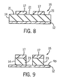
- a second light source 28 provides flood exposure of radiation 30 at a longer lithographic or exposure wavelength of, for example, 248 nm.
- the wavelength of radiation 30 and layer 14 are selected such that exposed areas of layer 14 (i.e., areas not covered by polymerized areas or regions 17) are transparent to radiation 30 and undergo a photochemical reaction to become soluble (soluble areas or regions 21 in FIG. 8 ), while areas underneath polymerized areas or regions 17 will not be exposed to radiation 30 due to the opaqueness of polymerized areas or regions 17 and remain insoluble (insoluble areas or regions 23 in FIG. 8 ).
- First and second light sources 18, 28 can be the same light source that emits radiation at two wavelengths, i.e., the short and long UV lithographic wavelengths.
- light source 28 can be an excimer laser, an ND:YAG laser, a frequency multiplied ND:YAG laser, a He-Ne scanning laser, or other light source. There may also be provided additional components or equipment between light source 28 and portion 10 to provide desirable radiation 30 to layer 14.
- the pattern or image provided on mask 20 will be fully transferred to photoresist layer 14 at a resolution determined by the first exposure step.
- the exposed areas of layer 14 are soluble areas or regions 21 and the non-exposed areas of layer 14 or regions 23 ( FIG. 9 ) (due to polymerized areas or regions 17) become insoluble areas (see FIGS. 8 and 9 ).
- soluble areas or regions 21 of layer 14 are removed such that only cross-linked areas or regions 17 and insoluble areas or regions 23 of layer 14 remain on substrate 12 ( FIG. 9 ).
- the developing step utilizes a solvent developer conventionally selected to develop material comprising layer 14.
- photoresist used for 248 nm lithography can use a 0.24N tetramethylammonium hydroxide developer to remove soluble areas or regions 21.
- polymerized areas or regions 17 become insoluble upon exposure to short lithographic wavelength radiation.
- polymerized areas or regions 17 may undergo further chemical changes upon exposure to long lithographic wavelength radiation as long as it functions as a mask during the second exposure step.
- polymerized areas or regions 17 remain after the developing step and aid in subsequent processing steps such as an etching step or a deposition step involving portion 10.
- Regions 17 can improve etch stability of the top layer relative to the photoresist layer during anisotropic etching because it can be converted to silicon dioxide (SiO2) under plasma etching conditions.
- a photoresist conventionally used in longer wavelength lithography can be patterned with radiation of a short lithographic wavelength. Even further, the pattern resolution is smaller than those achievable with longer wavelength lithography, pattern resolution on the order of the short lithographic wavelength. Even still further, possible mask overlay or alignment problems are obviated through a self-aligned mask generated during the patterning process.
- a line 102 represents the absorbance (1/[mu]m) on a Y-axis 110 across X-axis 108 (wavelength [lambda]1).
- a line 102 similarly represents absorbance of poly(1-phenyl-1-phenyl-t-butylether siloxane)
- line 104 represents poly(phenyl-t-butylether siloxane)
- a line 106 similarly represents absorbance of poly(benzyl-t-butylether siloxane).
Abstract
Description
- The present invention relates generally to self-aligned pattern formation. More particularly, the present invention relates to self-aligned pattern formation using dual wavelengths to achieve smaller resolution than is achievable by conventional ultraviolet (UV) lithography.
- The semiconductor or IC industry aims to manufacture integrated circuits (ICs) with higher and higher densities of devices on a smaller chip area to achieve greater functionality and to reduce manufacturing costs. This desire for large scale integration has led to a continued shrinking of circuit dimensions and device features. The ability to reduce the size of structures, such as, gate lengths in field-effect transistors and the width of conductive lines, is driven by lithographic performance.
- Semiconductor fabrication techniques often utilize a photomask (also referred to as a mask) or a reticle. Radiation is provided through or reflected off the mask or reticle to form an image on a semiconductor wafer. Generally, the image is focused on the wafer to pattern a layer of material, such as, photoresist material. In turn, the photoresist material is utilized to define doping regions, deposition regions, etching regions, or other structures associated with integrated circuits (ICs). The photoresist material can also define conductive lines or conductive pads associated with metal layers of an integrated circuit. Further, the photoresist material can define isolation regions, transistor gates, or other transistor structures and elements.
- To transfer an image or pattern onto the photoresist material, a conventional lithographic system generally includes a light source configured to provide electromagnetic radiation or light at one or more wavelengths. The light source may produce radiation at a wavelength of 365 nanometers (nm), 248 nm, and/or 193 nm. The photoresist material patterned by such radiation is selected to be responsive at the wavelength of such radiation. Preferably, the areas of the photoresist material upon which radiation is incident undergo a photochemical change such that it becomes suitably soluble or insoluble in a subsequent developing process step.
- Because the resolution of features is, in part, proportional to the exposure wavelength, it is desirable to pattern photoresist material using shorter exposure wavelengths (e.g., 157 nm, 126 nm, or 13 4 nm). Unfortunately, few, if any, materials or processes can consistently fabricate semiconductor integrated devices at such shorter wavelengths. Attempts to use conventional photoresist materials, such as organic based photoresist materials, used in 365 nm, 248 nm, or 193 nm lithographic systems are not without problems. Organic based photoresist materials exhibit high optical absorption per unit thickness in single layer patterning applications at the shorter lithographic or exposure wavelengths. Thus, conventional organic based photoresist materials become increasingly opaque to the exposing radiation and the necessary photochemical change does not occur throughout the entire thickness of the material.
- To overcome this drawback, a thinner layer of conventional photoresist material (relative to the thickness used in longer wavelength lithography) has been tried with shorter lithographic wavelengths. Unfortunately, the use of a thinner layer of photoresist material is problematic especially during etch processing. Among others, using a thinner layer results in low pattern fidelity, thin film instability problems, and/or inadequate imaging performance.
-
EP0366 503 discloses chemical compositions which provide an increased rate of processing during photolithography. -
EP1176468 discloses a masking layer for etching semiconductor substrates. - Thus, there is a need for a system and method for effectively extending the use of conventional photoresist materials to shorter lithographic wavelengths in the deep ultraviolet (DUV) or extreme ultraviolet (EUV) range. There is a further need for a system and method of pattern formation that achieves the feature resolutions of shorter lithographic wavelengths without extensive modifications to conventional lithographic techniques, materials, or equipment. Even further still, there is a need for a process or method that provides pattern self alignment and obviates the need for mask overlay.
- An exemplary embodiment relates to an integrated circuit fabrication process. The process includes exposing a bi-layer photoresist material with two distinct layers, a first layer of which including arylalkoxysilane, the bi-layer provided over a substrate to a first radiation at a first lithographic wavelength, through a mask. Treating the first layer with a solvent to remove unexposed parts of the first layer. The process further includes exposing the bi-layer photoresist material to a second radiation at a second lithographic wavelength. The first lithographic wavelength is shorter than the second lithographic wavelength and the exposing step with the first radiation is performed before the exposing step with the second radiation. The transformed top portion of the photoresist material is non-transparent to the second radiation.
- The preferred embodiment will become more fully understood from the following detailed description, taken in conjunction with the accompanying drawings,
wherein like reference numerals denote like elements, in which -
FIG. 1 is a cross-sectional view showing a lipophilic photoresist layer on top of a silicon wafer substrate; -
FIG. 2 is a cross-sectional view of a film of organotrialkoxysilane, photobase generator, and catalytic amount of water on top of the lipophilic photoresist layer -
FIG. 3 is a cross-sectional view of the portion of the integrated circuit illustrated inFIG. 2 , showing a first exposure step at wavelength λ1; -
FIG. 4 is a cross-sectional view of the portion of the integrated circuit illustrated inFIG. 3 , showing the polymerization of the exposed parts of organoarylalkoxysilane layer by the photogenerated base from the photobase generator and catalytic amount of water at first exposure step at wavelength λ1; -
FIG. 5 is a cross-sectional view of the portion of the integrated circuit illustrated inFIG. 4 , showing a self-aligned pattern formation step, following the washing away of the unpolymerized organoarylalkoxysilane with water/methanol solution; -
FIG. 6 is a cross-sectional view of the portion of the integrated circuit illustrated inFIG. 5 , showing a self-aligned pattern formation step, following the baking of the polymerized organoarylalkoxysilane layer; -
FIG. 7 is a cross-sectional view of the portion of the integrated circuit illustrated inFIG. 6 , showing a flood exposure step at wavelength λ2; -
FIG. 8 is a cross-sectional view of the portion of the integrated circuit illustrated inFIG. 7 showing a post-exposure bake step; -
FIG. 9 is a cross-sectional view of the portion of the integrated circuit illustrated inFIG. 8 showing a develop step; and -
Figure 10 is plot of absorption spectra of representative organoarylalkoxysilane from 150 nm to 200 nm. - With reference to
FIGs. 1-10 , an exemplary embodiment of an advantageous scheme for self aligning a pattern onto a photoresist material will be described. The advantageous scheme also provides sub-lithographic feature resolution on the order smaller than the resolution limit of the first wavelength λ1 (the shorter of the dual wavelengths). - With reference to
FIG. 1 , a first exposure step comprising the advantageous process is performed on a portion of an integrated circuit (IC). The portion includes aphotoresist layer 14 provided on asubstrate 12.Substrate 12 can be an IC wafer, a semiconductive material, an insulative material, a conductive material, layers above any of the listed materials, or a base layer.Substrate 12 can be an industry standard silicon wafer.Substrate 12 is not described in a limiting fashion. -
Substrate 12 can include insulative, conductive, or semiconductive layers above or below its top surface. The insulative, conductive or semiconductive layers can be deposited or grown onsubstrate 12 or on layers above layers onsubstrate 12. Although shown directly abovesubstrate 12,layer 14 can be provided above base layers, intermediate layers, anti-reflective coatings, or other layers. -
Photoresist layer 14 is selected to have photochemical reactions in response toelectromagnetic radiation 16 from a first light source 18 (FIG. 3 ).Photoresist layer 14 can be any conventional positive photoresist material. Preferably,photoresist layer 14 is comprised of a 193-nm or 248-nm wavelength photosensitive lipophilic polymeric material with the appropriate photoacid generator applied tosubstrate 12 at a thickness of 100-500 nm by spin coating. -
First light source 18 can be any number of sources of electromagnetic radiation. Firstlight source 18 can be a single light source or multiple light sources for providingradiation 16 at a short wavelength. Preferably,first light source 18 providesradiation 16 at a short wavelength (193 nm, 248 nm) in the deep ultraviolet (DUV) or vacuum ultraviolet (157 nm, 126 nm), or extreme ultraviolet (EUV) range, such as, 11.4 nm, 13.4 nm. The short wavelength λ1 of radiation 16 (also referred to as the short lithographic wavelength) preferably can polymerize organotrialkoxysilane monomers such as aryltriethoxysilane in the presence of photobase generators (PBG) such as o-nitrobenzoyl carbamates and urethanes, o-acyloxime, benzoin carbamate, oxime-urethanes, etc. and catalytic amount of water, as shown in Equation 1 below:
- First
light source 18 can be a laser light source such as an F2 excimer laser (157 nm) , XeCl laser, ArF excimer laser (193 nm), KrF laser (248 nm), or laser-produced Xe plasma (13.4 nm, 11.4 nm) or discharge-produced plasma (at 13.4 nm, 11.4 nm) or other radiations such as electron beam, ion beam, gamma ray, etc. Alternatively,light source 18 can be a laser light source that emits two or more wavelengths in various wavelength ranges, such as, an argon laser. -
Radiation 16 from firstlight source 18 is provided via a mask orreticle 20 in accordance with a pattern on mask orreticle 20 tophotoresist layer 14. Mask orreticle 20 is preferably a conventional photomask or reticle including a glass substrate (e.g., fused silica) and an opaque material (e.g., chromium). Although not shown, there may also be other components or equipment provided betweenlight source 18 and photoresist layer14 to transfer the image onmask 20 tophotoresist layer 14, such as, an optical system (e.g., one or more lens assemblies). - In one embodiment, a film 15 (
FIG. 2 ) of arylalkoxysilane monomer with a photobase generator, and catalytic amount of water is coated on top of thelipophilic photoresist layer 14 and exposed to the short wavelength light λ1. If necessary, a few monolayers of an adhesion promoter like hexamethyldisilazane may be coated on top of the photoresist to improve the adhesion of the arylalkoxysilane monomer to the photoresist. Examples of arylalkoxysilane monomers are: pheny-t-butyl- ether triethoxysilane, 1-phenyl-1-phenyl-t-butylether diethoxysilane, and benzyl-t-butylether triethoxysilane. These monomers can be combined or mixed depending on desired characteristics. Preferably, the monomer has available bonds associated with the Si atoms that can be activated to promote polymerization by short wavelength exposure and subsequent developments. The monomer preferably has a profile of light absorbance as a function of the wavelength in which absorbance is lower at the shorter wavelengths to achieve current resolution goals and absorbance is higher at the longer wavelength to which more conventional resists are sensitive. Although these characteristics are preferred, the characteristics are not necessarily required for a photoresist material to fall within the scope of any claim unless explicitly required by the claim. - Upon exposure through a photomask (mask 20), the photobase generator generates a photobase, which catalyzes the polymerization of the arylalkoxysilane monomer in the presence of water in the exposed part of film 15 (
FIGs. 3 and4 ). While the arylalkoxysilane monomer (see regions 19) is reasonably transparent at 157 nm, the poly(arylalkoxysilane) is quite opaque (see regions 17). The absorbance of the poly(arylalkoxysilane) (regions 17) is significantly higher at 193 nm than at 157 nm (seeFigure 10 ). - Washing the arylalkoxysilane /poly(arylalkoxysilane layer (
layer 15 includingregions 17 and 19) with water/methanol mixture removes the unpolymerized arylalkoxysilane monomer (region 19) from the unexposed part, leaving the poly(arylalkoxysilane) (region 17) in the exposed part of film 15 (FIG. 5 ). Baking at an appropriate temperature drives off the residual solvent, leaving a top layer with poly(arylalkoxysilane), which effectively serves as a mask for the subsequent exposure step (FIG. 6 ). - Flood exposing the self-aligned mask/photoresist combination (
layer 14 and film 15) at a longer wavelength λ2 effectively transforms the unmasked sections (regions 21) of the photoresist layer, in a self-aligned mask fashion (FIG. 7 ). Applying the conventional post-applied bake (FIG. 8 ), followed by solvent development in an aqueous base like tetramethylammonium hydroxide (TMAH), washes the exposed part of the photoresist, leaving self-aligned masked patterns of theunexposed sections 23 of the photoresist. (FIG. 9 ) -
Photoresist layer 14 is preferably a positive photoresist that is transparent to radiation at longer ultraviolet (UV) wavelengths (e.g., 365 nm, 248 nm, or 193 nm) and is marginally or semi-transparent to radiation at shorter wavelengths (e.g., 157 nm, 126 nm, or 13.4 nm). For example,photoresist layer 14 can be a photoresist conventionally used in 193 nm lithography, such as Sumitomo Chemical's PAR720™, PAR707™, or a photoresist used in 248 nm lithography such as Shipley's UV110™ - an environmentally stable chemically amplified photoresist (ESCAP). -
Film 15 andphotoresist layer 14 form a bi-layer photoresist with two distinct and separate layers. The top layer (film 15) polymerizes and becomes opaque at longer wavelengths to which the bottom layer (layer 14) is sensitive. The bottom layer can be a more conventional photoresist material and unlike the top layer, the bottom layer cannot be patterned efficiently by the shorter wavelength radiation. - After the first exposure step of
FIG. 3 , pattern transfer frommask 20 has occurred, as represented by polymerized areas orregions 17 oflayer 14.Polymerized areas 17 have feature resolution on the order of approximately one-half the wavelength to the wavelength of the short exposure wavelength ofradiation 16. Continuing the example, polymerizedregion 17 created by exposure to a 157 nm radiation has a feature resolution of approximately 72-157 nm. Alternatively,radiation 16 at a wavelength of 126 or 13.4 nm would result in a possible resolution of approximately 63-126 nm or 6.7-13.4 nm, respectively. - Polymerized areas or
regions 17 are preferably opaque or non-transparent to radiation at longer lithographic wavelengths (e.g., 365, 248, or 193 nm) conventionally used to exposephotoresist layer 14. Such opaqueness permits polymerized areas orregions 17 to serve as a self-aligned mask or reticle in a longer wavelength exposure step involving portion 10 (FIG. 7 ). - In a second exposure step (
FIG. 7 ), mask 20 (FIG. 3 ) is no longer needed to transfer a pattern ontoportion 10. Instead, polymerized areas orregions 17 offilm 15 advantageously serve as a self-aligned mask of the pattern or image provided bymask 20. A secondlight source 28 provides flood exposure ofradiation 30 at a longer lithographic or exposure wavelength of, for example, 248 nm. The wavelength ofradiation 30 andlayer 14 are selected such that exposed areas of layer 14 (i.e., areas not covered by polymerized areas or regions 17) are transparent toradiation 30 and undergo a photochemical reaction to become soluble (soluble areas orregions 21 inFIG. 8 ), while areas underneath polymerized areas orregions 17 will not be exposed toradiation 30 due to the opaqueness of polymerized areas orregions 17 and remain insoluble (insoluble areas orregions 23 inFIG. 8 ). - First and second
light sources light source 28 can be an excimer laser, an ND:YAG laser, a frequency multiplied ND:YAG laser, a He-Ne scanning laser, or other light source. There may also be provided additional components or equipment betweenlight source 28 andportion 10 to providedesirable radiation 30 tolayer 14. - Accordingly, after the second exposure step, the pattern or image provided on
mask 20 will be fully transferred tophotoresist layer 14 at a resolution determined by the first exposure step. The exposed areas oflayer 14 are soluble areas orregions 21 and the non-exposed areas oflayer 14 or regions 23 (FIG. 9 ) (due to polymerized areas or regions 17) become insoluble areas (seeFIGS. 8 and 9 ). In a developing step, soluble areas orregions 21 oflayer 14 are removed such that only cross-linked areas orregions 17 and insoluble areas orregions 23 oflayer 14 remain on substrate 12 (FIG. 9 ). Preferably, the developing step utilizes a solvent developer conventionally selected to developmaterial comprising layer 14. For example, photoresist used for 248 nm lithography can use a 0.24N tetramethylammonium hydroxide developer to remove soluble areas orregions 21. - In the preferred embodiment, polymerized areas or
regions 17 become insoluble upon exposure to short lithographic wavelength radiation. Alternatively, it should be understood that polymerized areas orregions 17 may undergo further chemical changes upon exposure to long lithographic wavelength radiation as long as it functions as a mask during the second exposure step. Preferably, polymerized areas orregions 17 remain after the developing step and aid in subsequent processing steps such as an etching step or a depositionstep involving portion 10.Regions 17 can improve etch stability of the top layer relative to the photoresist layer during anisotropic etching because it can be converted to silicon dioxide (SiO2) under plasma etching conditions. - In this manner, an advantageous scheme for achieving small feature resolutions using conventional equipment and materials is described herein. Using sequential radiation of differing wavelengths, a short lithographic wavelength followed by a longer lithographic wavelength, a photoresist conventionally used in longer wavelength lithography can be patterned with radiation of a short lithographic wavelength. Even further, the pattern resolution is smaller than those achievable with longer wavelength lithography, pattern resolution on the order of the short lithographic wavelength. Even still further, possible mask overlay or alignment problems are obviated through a self-aligned mask generated during the patterning process.
- With reference to
FIG. 10 , the absorber of arylsiloxane materials with respect to wavelength is shown. Aline 102 represents the absorbance (1/[mu]m) on a Y-axis 110 across X-axis 108 (wavelength [lambda]1). Aline 102 similarly represents absorbance of poly(1-phenyl-1-phenyl-t-butylether siloxane),line 104 represents poly(phenyl-t-butylether siloxane), and aline 106 similarly represents absorbance of poly(benzyl-t-butylether siloxane). The change or difference in absorbance at 193 nm with respect to the absorbance at 157 nm advantageously allows a superior lithographic process to be designed.
Claims (5)
- An integrated circuit fabrication process, the process characterized by:exposing a bi-layer photoresist material with two distinct layers (14, 15), a first layer of which including arylalkoxysilane (15), said bi-layer provided over a substrate, to a first radiation (116) at a first lithographic wavelength (λ1) through a mask (20);treating said first layer (15) with a solvent to remove unexposed parts (19) of said first layer (15);exposing the bi-layer photoresist material to a second radiation (30) at a second lithographic wavelength (λ2),wherein the first lithographic wavelength (λ1) is shorter than the second lithographic wavelength (λ2) and the transformed top portion of the photoresist material (15) being non-transparent to the second radiation (λ2), and the exposing step with the first radiation is performed before the exposing step with the second radiation.
- The process of claim 1, characterized in that the second lithographic wavelength is selected from a wavelength including 365 nm, 248 nm, and 193 nm.
- The process of claims 1 or 2, further characterized by providing the transformed top portion of the photoresist material (14) as a self-aligned mask for the exposing step with the second radiation.
- The process of claim 3, characterized in that the transformed top portion of the photoresist material comprises polymerized organoarylalkoxysilane material.
- The process of claim 4, characterized in that the thickness of the transformed top portion is at least 10 nm.
Applications Claiming Priority (3)
| Application Number | Priority Date | Filing Date | Title |
|---|---|---|---|
| US10/083,914 US6764808B2 (en) | 2002-02-27 | 2002-02-27 | Self-aligned pattern formation using wavelenghts |
| US83914 | 2002-02-27 | ||
| PCT/US2003/004960 WO2003073165A2 (en) | 2002-02-27 | 2003-02-21 | Self-aligned pattern formation using dual wavelengths |
Publications (2)
| Publication Number | Publication Date |
|---|---|
| EP1478978A2 EP1478978A2 (en) | 2004-11-24 |
| EP1478978B1 true EP1478978B1 (en) | 2009-09-23 |
Family
ID=27753386
Family Applications (1)
| Application Number | Title | Priority Date | Filing Date |
|---|---|---|---|
| EP03743156A Expired - Lifetime EP1478978B1 (en) | 2002-02-27 | 2003-02-21 | Self-aligned pattern formation using dual wavelengths |
Country Status (9)
| Country | Link |
|---|---|
| US (1) | US6764808B2 (en) |
| EP (1) | EP1478978B1 (en) |
| JP (1) | JP2005519456A (en) |
| KR (1) | KR20040094706A (en) |
| CN (1) | CN1299166C (en) |
| AU (1) | AU2003211152A1 (en) |
| DE (1) | DE60329371D1 (en) |
| TW (1) | TWI278013B (en) |
| WO (1) | WO2003073165A2 (en) |
Families Citing this family (16)
| Publication number | Priority date | Publication date | Assignee | Title |
|---|---|---|---|---|
| DE10138105A1 (en) * | 2001-08-03 | 2003-02-27 | Infineon Technologies Ag | Photoresist and method for structuring such a photoresist |
| US7501230B2 (en) * | 2002-11-04 | 2009-03-10 | Meagley Robert P | Photoactive adhesion promoter |
| DE10309266B3 (en) * | 2003-03-04 | 2005-01-13 | Infineon Technologies Ag | A method of forming an opening of a light absorbing layer on a mask |
| DE10310781A1 (en) * | 2003-03-12 | 2004-09-30 | Infineon Technologies Ag | Method for operating a microprocessor and a microprocessor arrangement |
| US7265366B2 (en) * | 2004-03-31 | 2007-09-04 | Asml Netherlands B.V. | Lithographic apparatus and device manufacturing method |
| WO2006085741A1 (en) * | 2005-02-09 | 2006-08-17 | Stichting Dutch Polymer Institute | Process for preparing a polymeric relief structure |
| US7816072B2 (en) * | 2005-05-02 | 2010-10-19 | Tokyo Ohka Kogyo Co., Ltd. | Positive resist composition and method for forming resist pattern |
| US20070166649A1 (en) * | 2006-01-18 | 2007-07-19 | Cheng-Hung Yu | Method of forming a micro device |
| CN100465666C (en) * | 2006-01-24 | 2009-03-04 | 联华电子股份有限公司 | Manufacture method of microcomponent |
| JP2007287928A (en) * | 2006-04-17 | 2007-11-01 | Nec Electronics Corp | Semiconductor integrated circuit, its manufacturing method, and mask |
| JP4660826B2 (en) * | 2006-08-18 | 2011-03-30 | 山栄化学株式会社 | Method for forming resist pattern |
| US7863150B2 (en) * | 2006-09-11 | 2011-01-04 | International Business Machines Corporation | Method to generate airgaps with a template first scheme and a self aligned blockout mask |
| KR101023077B1 (en) * | 2008-10-27 | 2011-03-24 | 주식회사 동부하이텍 | method of forming mask pattern |
| US9977339B2 (en) | 2014-01-27 | 2018-05-22 | Tokyo Electron Limited | System and method for shifting critical dimensions of patterned films |
| US9645495B2 (en) | 2014-08-13 | 2017-05-09 | Tokyo Electron Limited | Critical dimension control in photo-sensitized chemically-amplified resist |
| US11294273B2 (en) * | 2019-10-25 | 2022-04-05 | Innolux Corporation | Mask substrate and method for forming mask substrate |
Citations (1)
| Publication number | Priority date | Publication date | Assignee | Title |
|---|---|---|---|---|
| EP1176468A1 (en) * | 2000-07-26 | 2002-01-30 | France Telecom | Resin bilayer for extreme ultraviolet photolithography and extreme ultraviolet photololithographic method |
Family Cites Families (9)
| Publication number | Priority date | Publication date | Assignee | Title |
|---|---|---|---|---|
| EP0098922A3 (en) | 1982-07-13 | 1986-02-12 | International Business Machines Corporation | Process for selectively generating positive and negative resist patterns from a single exposure pattern |
| US4810601A (en) * | 1984-12-07 | 1989-03-07 | International Business Machines Corporation | Top imaged resists |
| NL8500455A (en) | 1985-02-18 | 1986-09-16 | Philips Nv | METHOD FOR MANUFACTURING A SEMICONDUCTOR DEVICE, FORMING A PHOTOGRAPHIC MASK USING A TWO-LAYER PAINTING SYSTEM |
| JPH02269353A (en) | 1988-10-28 | 1990-11-02 | Hewlett Packard Co <Hp> | Method of manufacturing semiconductor by photolithography |
| US5180655A (en) * | 1988-10-28 | 1993-01-19 | Hewlett-Packard Company | Chemical compositions for improving photolithographic performance |
| JP3192879B2 (en) * | 1994-07-28 | 2001-07-30 | トヨタ自動車株式会社 | Ceramic butterfly valve and method of manufacturing the same |
| JPH09319097A (en) * | 1996-01-16 | 1997-12-12 | Sumitomo Chem Co Ltd | Method for forming resist pattern |
| JP3373147B2 (en) * | 1998-02-23 | 2003-02-04 | シャープ株式会社 | Photoresist film and pattern forming method thereof |
| WO2003095026A1 (en) | 2002-05-13 | 2003-11-20 | Pflueger D Russell | Spinal disc therapy system |
-
2002
- 2002-02-27 US US10/083,914 patent/US6764808B2/en not_active Expired - Lifetime
-
2003
- 2003-02-21 WO PCT/US2003/004960 patent/WO2003073165A2/en active Application Filing
- 2003-02-21 EP EP03743156A patent/EP1478978B1/en not_active Expired - Lifetime
- 2003-02-21 CN CNB038025280A patent/CN1299166C/en not_active Expired - Fee Related
- 2003-02-21 DE DE60329371T patent/DE60329371D1/en not_active Expired - Lifetime
- 2003-02-21 AU AU2003211152A patent/AU2003211152A1/en not_active Abandoned
- 2003-02-21 JP JP2003571795A patent/JP2005519456A/en active Pending
- 2003-02-21 KR KR10-2004-7012948A patent/KR20040094706A/en active Search and Examination
- 2003-02-27 TW TW092104154A patent/TWI278013B/en not_active IP Right Cessation
Patent Citations (2)
| Publication number | Priority date | Publication date | Assignee | Title |
|---|---|---|---|---|
| EP1176468A1 (en) * | 2000-07-26 | 2002-01-30 | France Telecom | Resin bilayer for extreme ultraviolet photolithography and extreme ultraviolet photololithographic method |
| US20020072014A1 (en) * | 2000-07-26 | 2002-06-13 | Andre Schiltz | Resin, a double resin layer for extreme ultraviolet light (EUV) photolithography, and an extreme ultraviolet light (EUV) photolithography process |
Also Published As
| Publication number | Publication date |
|---|---|
| AU2003211152A1 (en) | 2003-09-09 |
| US20030162135A1 (en) | 2003-08-28 |
| TW200303573A (en) | 2003-09-01 |
| CN1299166C (en) | 2007-02-07 |
| DE60329371D1 (en) | 2009-11-05 |
| TWI278013B (en) | 2007-04-01 |
| WO2003073165A3 (en) | 2003-10-16 |
| WO2003073165A2 (en) | 2003-09-04 |
| EP1478978A2 (en) | 2004-11-24 |
| KR20040094706A (en) | 2004-11-10 |
| US6764808B2 (en) | 2004-07-20 |
| CN1620634A (en) | 2005-05-25 |
| JP2005519456A (en) | 2005-06-30 |
Similar Documents
| Publication | Publication Date | Title |
|---|---|---|
| KR100639680B1 (en) | Forming method of fine patterns for semiconductor device | |
| US6905621B2 (en) | Method for preventing the etch transfer of sidelobes in contact hole patterns | |
| US9012132B2 (en) | Coating material and method for photolithography | |
| TWI476816B (en) | Self-aligned spacer multiple patterning methods | |
| EP1478978B1 (en) | Self-aligned pattern formation using dual wavelengths | |
| KR20100102189A (en) | Multiple exposure photolithography methods and photoresist compositions | |
| US20100173247A1 (en) | Substrate planarization with imprint materials and processes | |
| JP2000315647A (en) | Formation of resist pattern | |
| EP0935172A1 (en) | Photosensitive resin, resist based on the photosensitive resin, exposure method using the resist, and semiconductor device obtained by the exposure method | |
| US6943124B1 (en) | Two step exposure to strengthen structure of polyimide or negative tone photosensitive material | |
| US20230384683A1 (en) | Photoresist with polar-acid-labile-group | |
| US20130330672A1 (en) | Method for enhancing lithographic imaging of isolated and semi-isolated features | |
| KR20150126766A (en) | Method of preparing and using photosensitive material | |
| US7169716B2 (en) | Photosensitive lacquer for providing a coating on a semiconductor substrate or a mask | |
| JPH10301268A (en) | Reflection preventing film material | |
| CN108231550B (en) | Method for manufacturing semiconductor device | |
| US5275913A (en) | Method for preparing resist patterns utilizing solvent development with subsequent resist pattern transfer, via a photo-hardening liquid adhesive, to a receiver substrate and oxygen reactive ion etching | |
| JP2004045969A (en) | Pattern forming material and pattern forming method | |
| Kudo et al. | Latest developments in photosensitive developable bottom anti-reflective coating (DBARC) | |
| US20040265748A1 (en) | Pattern transfer of an extreme ultraviolet imaging layer via flood exposure of contact mask layer (EUV CML) | |
| KR100772784B1 (en) | Phase Shift Mask for Performing Exposure Process using Extreme Ultra-Violet Light Source and Method for Manufacturing the its | |
| KR20040079756A (en) | Method for Forming Micro Pattern of Semiconductor Device | |
| KR19990061090A (en) | Photoresist for multilayer resist process and fine pattern manufacturing method of semiconductor device using same | |
| Rubner et al. | Photoresists | |
| Richter et al. | CARL–advantages of thin-film imaging for leading-edge lithography |
Legal Events
| Date | Code | Title | Description |
|---|---|---|---|
| PUAI | Public reference made under article 153(3) epc to a published international application that has entered the european phase |
Free format text: ORIGINAL CODE: 0009012 |
|
| 17P | Request for examination filed |
Effective date: 20040729 |
|
| AK | Designated contracting states |
Kind code of ref document: A2 Designated state(s): AT BE BG CH CY CZ DE DK EE ES FI FR GB GR HU IE IT LI LU MC NL PT SE SI SK TR |
|
| AX | Request for extension of the european patent |
Extension state: AL LT LV MK RO |
|
| 17Q | First examination report despatched |
Effective date: 20081015 |
|
| GRAP | Despatch of communication of intention to grant a patent |
Free format text: ORIGINAL CODE: EPIDOSNIGR1 |
|
| GRAS | Grant fee paid |
Free format text: ORIGINAL CODE: EPIDOSNIGR3 |
|
| GRAA | (expected) grant |
Free format text: ORIGINAL CODE: 0009210 |
|
| AK | Designated contracting states |
Kind code of ref document: B1 Designated state(s): DE FR GB |
|
| REG | Reference to a national code |
Ref country code: GB Ref legal event code: FG4D |
|
| REF | Corresponds to: |
Ref document number: 60329371 Country of ref document: DE Date of ref document: 20091105 Kind code of ref document: P |
|
| RAP2 | Party data changed (patent owner data changed or rights of a patent transferred) |
Owner name: GLOBALFOUNDRIES, INC. |
|
| PLBE | No opposition filed within time limit |
Free format text: ORIGINAL CODE: 0009261 |
|
| STAA | Information on the status of an ep patent application or granted ep patent |
Free format text: STATUS: NO OPPOSITION FILED WITHIN TIME LIMIT |
|
| 26N | No opposition filed |
Effective date: 20100624 |
|
| REG | Reference to a national code |
Ref country code: FR Ref legal event code: ST Effective date: 20101029 |
|
| PG25 | Lapsed in a contracting state [announced via postgrant information from national office to epo] |
Ref country code: FR Free format text: LAPSE BECAUSE OF NON-PAYMENT OF DUE FEES Effective date: 20100301 |
|
| PGFP | Annual fee paid to national office [announced via postgrant information from national office to epo] |
Ref country code: GB Payment date: 20110124 Year of fee payment: 9 |
|
| PGFP | Annual fee paid to national office [announced via postgrant information from national office to epo] |
Ref country code: DE Payment date: 20120215 Year of fee payment: 10 |
|
| GBPC | Gb: european patent ceased through non-payment of renewal fee |
Effective date: 20120221 |
|
| PG25 | Lapsed in a contracting state [announced via postgrant information from national office to epo] |
Ref country code: GB Free format text: LAPSE BECAUSE OF NON-PAYMENT OF DUE FEES Effective date: 20120221 |
|
| REG | Reference to a national code |
Ref country code: DE Ref legal event code: R119 Ref document number: 60329371 Country of ref document: DE Effective date: 20130903 |
|
| PG25 | Lapsed in a contracting state [announced via postgrant information from national office to epo] |
Ref country code: DE Free format text: LAPSE BECAUSE OF NON-PAYMENT OF DUE FEES Effective date: 20130903 |