JP2005257740A - Projection optical system, exposing device, and exposure method - Google Patents
Projection optical system, exposing device, and exposure method Download PDFInfo
- Publication number
- JP2005257740A JP2005257740A JP2004065375A JP2004065375A JP2005257740A JP 2005257740 A JP2005257740 A JP 2005257740A JP 2004065375 A JP2004065375 A JP 2004065375A JP 2004065375 A JP2004065375 A JP 2004065375A JP 2005257740 A JP2005257740 A JP 2005257740A
- Authority
- JP
- Japan
- Prior art keywords
- exposure
- optical system
- projection optical
- partial
- mask
- Prior art date
- Legal status (The legal status is an assumption and is not a legal conclusion. Google has not performed a legal analysis and makes no representation as to the accuracy of the status listed.)
- Withdrawn
Links
Images


Landscapes
- Lenses (AREA)
- Exposure And Positioning Against Photoresist Photosensitive Materials (AREA)
- Exposure Of Semiconductors, Excluding Electron Or Ion Beam Exposure (AREA)
Abstract
Description
本発明は、投影光学系、露光装置、および露光方法に関し、特に半導体素子などをフォトリソグラフィ工程で製造する際に使用される露光装置に好適な投影光学系に関するものである。 The present invention relates to a projection optical system, an exposure apparatus, and an exposure method, and more particularly to a projection optical system suitable for an exposure apparatus used when manufacturing a semiconductor element or the like in a photolithography process.
半導体素子等を製造するためのフォトリソグラフィ工程において、マスク(またはレチクル)のパターン像を、投影光学系を介して、感光性基板(フォトレジスト等が塗布されたウェハまたはガラスプレート等)上に露光する露光装置が使用されている。この種の露光装置として、例えば特公昭46−34057号公報には、スティッチング方式でスリットスキャン方式(以下、単に「スティッチング方式」という)の露光装置が開示されている。 In a photolithography process for manufacturing a semiconductor element or the like, a pattern image of a mask (or reticle) is exposed on a photosensitive substrate (a wafer or a glass plate coated with a photoresist or the like) via a projection optical system. An exposure apparatus is used. As this type of exposure apparatus, for example, Japanese Patent Publication No. 46-34057 discloses an exposure apparatus of a slit scanning type (hereinafter simply referred to as “stitching type”) in a stitching method.
スティッチング方式露光装置では、マスク上の所定形状の照明領域に対してマスクおよび感光性基板を第1方向に同期的に相対移動させることにより、感光性基板上の第1列目の部分露光領域への第1回目のスキャン露光(走査露光)を行う。その後、たとえばマスクを第1方向に垂直な第2方向に所定量だけ移動させるとともに、感光性基板を第2方向に共役な方向に横ずれ(スティッチング)させる。 In the stitching method exposure apparatus, the partial exposure region in the first row on the photosensitive substrate is obtained by synchronously moving the mask and the photosensitive substrate in the first direction with respect to the illumination region having a predetermined shape on the mask. The first scan exposure (scan exposure) is performed. Thereafter, for example, the mask is moved by a predetermined amount in a second direction perpendicular to the first direction, and the photosensitive substrate is laterally shifted (stitched) in a direction conjugate to the second direction.
そして、再びマスク上の所定形状の照明領域に対してマスクおよび感光性基板を第1方向に同期的に相対移動させることにより、感光性基板上の第2列目の部分露光領域への第2回目のスキャン露光を行う。こうして、スティッチング方式の露光装置では、第1列目の部分露光領域と第2列目の部分露光領域とを含む1つのショット領域、すなわち投影光学系のイメージフィールド(有効結像領域)よりも広い感光性基板上の領域に、マスクパターンが転写される。 Then, the mask and the photosensitive substrate are moved relative to each other in a first direction synchronously with respect to the illumination area having a predetermined shape on the mask again, so that the second exposure to the partial exposure region in the second row on the photosensitive substrate is performed. Perform the second scan exposure. Thus, in the stitching type exposure apparatus, one shot area including the first column partial exposure region and the second column partial exposure region, that is, an image field (effective imaging region) of the projection optical system. The mask pattern is transferred to an area on a wide photosensitive substrate.
上述したように、スティッチング方式の露光装置では、たとえばマスクを交換することなく2つの部分露光領域へのスキャン露光を行うことにより、投影光学系のイメージフィールドよりも広い1つのショット領域にマスクパターンを転写することができる。その結果、比較的小型の投影光学系を用いることによるコストの低減や、マスク交換が不要なことによるスループットの向上などを図ることができる。 As described above, in the stitching type exposure apparatus, for example, by performing scan exposure on two partial exposure regions without exchanging the mask, a mask pattern is formed on one shot region wider than the image field of the projection optical system. Can be transferred. As a result, the cost can be reduced by using a relatively small projection optical system, and the throughput can be improved by eliminating the need for mask replacement.
しかしながら、従来技術では、スティッチング方式の露光装置に好適な投影光学系の構成について具体的な提案がなされていない。なお、半導体素子等の集積度が向上するにつれて、露光装置の投影光学系に要求される解像力(解像度)が益々高まっている。そこで、露光装置の投影光学系では、その解像力に対する要求を満足するために、照明光(露光光)の波長を短くするとともに像側開口数を大きく確保する必要がある。 However, in the prior art, no specific proposal has been made regarding the configuration of a projection optical system suitable for a stitching type exposure apparatus. As the degree of integration of semiconductor elements and the like increases, the resolution (resolution) required for the projection optical system of the exposure apparatus is increasing. Therefore, in the projection optical system of the exposure apparatus, it is necessary to shorten the wavelength of the illumination light (exposure light) and ensure a large image-side numerical aperture in order to satisfy the requirement for the resolution.
本発明は、前述の課題に鑑みてなされたものであり、たとえばスティッチング方式の露光装置に適用可能な比較的小型の投影光学系を提供することを目的とする。また、本発明は、比較的小型の投影光学系を用いて、たとえばスティッチング方式の露光を行うことのできる露光装置および露光方法を提供することを目的とする。 The present invention has been made in view of the above-described problems, and an object thereof is to provide a relatively small projection optical system that can be applied to, for example, a stitching type exposure apparatus. It is another object of the present invention to provide an exposure apparatus and an exposure method that can perform, for example, stitching type exposure using a relatively small projection optical system.
前記課題を解決するために、本発明の第1形態では、第1面の縮小像を第2面上に形成する投影光学系において、
前記第1面における最大物高をφoとし、前記投影光学系中のすべてのレンズの有効径のうちの最大となる有効径の値をφmaxとするとき、
6.6<φmax/φo<12
の条件を満足することを特徴とする投影光学系を提供する。
In order to solve the above problems, in the first embodiment of the present invention, in the projection optical system for forming a reduced image of the first surface on the second surface,
When the maximum object height on the first surface is φo, and the maximum effective diameter value of all the effective diameters of the lenses in the projection optical system is φmax,
6.6 <φmax / φo <12
A projection optical system characterized by satisfying the above conditions is provided.
第1形態の好ましい態様によれば、前記投影光学系は、約|1/5|から約|1/4|の大きさの投影倍率を有する。また、前記投影光学系の光路中の雰囲気の屈折率を1とするとき、前記投影光学系と前記第2面との間の光路が1.1よりも大きい屈折率を有する媒質で満たされた状態で前記第1面の縮小像を前記第2面上に形成することが好ましい。 According to a preferred aspect of the first aspect, the projection optical system has a projection magnification of about | 1/5 | to about | 1/4 |. When the refractive index of the atmosphere in the optical path of the projection optical system is 1, the optical path between the projection optical system and the second surface is filled with a medium having a refractive index greater than 1.1. Preferably, a reduced image of the first surface is formed on the second surface in a state.
本発明の第2形態では、前記第1面に設定されたマスクを照明する照明工程と、第1形態の投影光学系を介して前記マスクに形成されたパターンの像を前記第2面に設定された感光性基板上に投影露光する露光工程とを備えていることを特徴とする露光方法を提供する。 In the second embodiment of the present invention, an illumination process for illuminating the mask set on the first surface, and an image of a pattern formed on the mask via the projection optical system of the first embodiment is set on the second surface. And an exposure step of performing projection exposure on the photosensitive substrate.
第2形態の好ましい態様によれば、前記露光工程では、2つの部分露光領域を含む1つのショット領域へ投影露光を行い、前記露光工程は、前記部分露光領域へ投影露光する部分露光工程を少なくとも2つ有し、前記部分露光工程では、前記投影光学系に対して前記マスクおよび前記感光性基板を相対移動させつつ前記部分露光領域への走査露光を行う。 According to a preferred aspect of the second aspect, in the exposure step, projection exposure is performed on one shot region including two partial exposure regions, and the exposure step includes at least a partial exposure step of performing projection exposure on the partial exposure region. In the partial exposure step, scanning exposure to the partial exposure region is performed while relatively moving the mask and the photosensitive substrate with respect to the projection optical system.
この場合、前記露光工程は、前記投影光学系に対して前記マスクおよび前記感光性基板を所定の向きに相対移動させつつ一方の部分露光領域への走査露光を行う第1回目の部分露光工程と、前記投影光学系に対して前記マスクおよび前記感光性基板を前記所定の向きと反対の向きに相対移動させつつ他方の部分露光領域への走査露光を行う第2回目の部分露光工程とを有することが好ましい。あるいは、前記露光工程は、前記投影光学系に対して前記マスクおよび前記感光性基板を所定の向きに相対移動させつつ一方の部分露光領域への走査露光を行う第1回目の部分露光工程と、前記投影光学系に対して前記マスクおよび前記感光性基板を前記所定の向きに相対移動させつつ他方の部分露光領域への走査露光を行う第2回目の部分露光工程とを有することが好ましい。 In this case, the exposure step includes a first partial exposure step of performing scanning exposure on one partial exposure region while relatively moving the mask and the photosensitive substrate in a predetermined direction with respect to the projection optical system. A second partial exposure step of performing scanning exposure on the other partial exposure region while relatively moving the mask and the photosensitive substrate in the direction opposite to the predetermined direction with respect to the projection optical system. It is preferable. Alternatively, the exposure step includes a first partial exposure step of performing scanning exposure on one partial exposure region while relatively moving the mask and the photosensitive substrate in a predetermined direction with respect to the projection optical system; It is preferable to include a second partial exposure step of performing scanning exposure on the other partial exposure region while relatively moving the mask and the photosensitive substrate in the predetermined direction with respect to the projection optical system.
また、第2形態の好ましい態様によれば、前記露光工程では、複数のショット領域へ投影露光を行い、前記露光工程は、前記複数のショット領域中の所定の前記部分露光領域へ投影露光する第1回目の部分露光工程と、前記複数のショット領域中の別の前記部分露光領域へ投影露光する第2回目の部分露光工程とを有する。また、前記第1回目の部分露光工程と前記第2回目の部分露光工程との間に前記マスクを交換しないことが好ましい。また、第2形態では、前記露光工程に先立って、前記投影光学系の光路中の雰囲気の屈折率を1とするとき、前記投影光学系と前記感光性基板との間の光路を1.1よりも大きい屈折率を有する媒質で満たす充填工程をさらに備えていることを特徴とする請求項4乃至9のいずれか1項に記載の露光方法ことが好ましい。 According to a preferred aspect of the second aspect, in the exposure step, projection exposure is performed on a plurality of shot regions, and the exposure step includes projection exposure on a predetermined partial exposure region in the plurality of shot regions. A first partial exposure step, and a second partial exposure step of performing projection exposure to another partial exposure region in the plurality of shot regions. Further, it is preferable that the mask is not exchanged between the first partial exposure process and the second partial exposure process. In the second embodiment, prior to the exposure step, when the refractive index of the atmosphere in the optical path of the projection optical system is 1, the optical path between the projection optical system and the photosensitive substrate is 1.1. The exposure method according to any one of claims 4 to 9, further comprising a filling step of filling with a medium having a larger refractive index.
本発明の第3形態では、前記第1面に設定されたマスクを照明するための照明系と、前記マスクに形成されたパターンの像を前記第2面に設定された感光性基板上に形成するための第1形態の投影光学系とを備えていることを特徴とする露光装置を提供する。 In the third aspect of the present invention, an illumination system for illuminating the mask set on the first surface and an image of a pattern formed on the mask are formed on the photosensitive substrate set on the second surface. An exposure apparatus is provided that includes the projection optical system according to the first embodiment.
第3形態の好ましい態様によれば、前記投影光学系に対して前記マスクおよび前記感光性基板を所定の方向に移動させつつ前記感光性基板への走査露光を行い、前記マスクを支持して前記所定の方向とほぼ直交する方向にステップ移動させるためのマスクステージをさらに備えている。 According to a preferred aspect of the third aspect, the photosensitive substrate is subjected to scanning exposure while moving the mask and the photosensitive substrate in a predetermined direction with respect to the projection optical system, and the mask is supported to support the mask. A mask stage for stepping in a direction substantially perpendicular to the predetermined direction is further provided.
本発明では、最大物高とレンズの最大有効径とに関する所定の条件式を満足しているので、たとえばスティッチング方式の露光装置に適用可能な比較的小型の投影光学系を実現することができる。したがって、本発明の露光装置および露光方法では、比較的小型の投影光学系を用いて、たとえばスティッチング方式の露光を行うことができ、ひいては良好なデバイスを製造することができる。 In the present invention, since a predetermined conditional expression relating to the maximum object height and the maximum effective diameter of the lens is satisfied, a relatively small projection optical system applicable to, for example, a stitching type exposure apparatus can be realized. . Therefore, in the exposure apparatus and the exposure method of the present invention, for example, a stitching type exposure can be performed using a relatively small projection optical system, and thus a good device can be manufactured.
本発明の投影光学系は、たとえば約1/5から約1/4の大きさ(絶対値)の投影倍率を有し、次の条件式(1)を満足する。条件式(1)において、φoは物体面(第1面)における最大物高であり、φmaxは投影光学系中のすべてのレンズの有効径のうちの最大となる有効径(直径)の値である。
6.6<φmax/φo<12 (1)
The projection optical system of the present invention has a projection magnification of about 1/5 to about 1/4 (absolute value), for example, and satisfies the following conditional expression (1). In conditional expression (1), φo is the maximum object height on the object surface (first surface), and φmax is the value of the maximum effective diameter (diameter) of the effective diameters of all the lenses in the projection optical system. is there.
6.6 <φmax / φo <12 (1)
条件式(1)の下限値を下回ると、物体側開口数が比較的大きいのでペッツバールの条件を満足することができなくなり、像の平坦性が悪くなってしまう。一方、条件式(1)の上限値を上回ると、光学系が径方向に大型化してしまう。すなわち、条件式(1)を満足することにより、投影光学系の大型化を招くことなく、2つの部分露光領域へのスキャン露光により1つの既定サイズのショット領域にマスクパターンを転写するのに必要な所要の大きさの有効結像領域(イメージフィールド)を確保することができる。 If the lower limit value of conditional expression (1) is not reached, the numerical aperture on the object side is relatively large, so that the Petzval condition cannot be satisfied, and the flatness of the image is deteriorated. On the other hand, if the upper limit of conditional expression (1) is exceeded, the optical system will be enlarged in the radial direction. That is, by satisfying conditional expression (1), it is necessary to transfer the mask pattern to one predetermined size shot area by scanning exposure to two partial exposure areas without increasing the size of the projection optical system. An effective imaging area (image field) having a required size can be ensured.
なお、本発明の効果をさらに良好に発揮するには、条件式(1)の下限値を8に設定し、上限値を11に設定することが好ましい。こうして、本発明では、たとえばスティッチング方式の露光装置に適用可能な比較的小型の投影光学系を実現することができる。したがって、本発明の露光装置および露光方法では、比較的小型の投影光学系を用いて、たとえばスティッチング方式の露光を行うことができる。 In order to achieve the effect of the present invention more satisfactorily, it is preferable to set the lower limit value of conditional expression (1) to 8 and the upper limit value to 11. Thus, according to the present invention, it is possible to realize a relatively small projection optical system applicable to, for example, a stitching type exposure apparatus. Therefore, the exposure apparatus and the exposure method of the present invention can perform, for example, stitching type exposure using a relatively small projection optical system.
なお、本発明では、投影光学系と感光性基板との間の光路中に1.1よりも大きい屈折率を有する媒質、たとえば液体(あるいは流体)のような高屈折率の媒質を介在させることが好ましい。この構成により、投影光学系の像側開口数の増大を、ひいては解像力の向上を図ることができる。また、本発明の露光装置および露光方法では、大きな実効的な像側開口数を有する高解像な投影光学系を用いて、解像度の高い良好な投影露光を行うことができる。 In the present invention, a medium having a refractive index larger than 1.1, for example, a medium having a high refractive index such as liquid (or fluid) is interposed in the optical path between the projection optical system and the photosensitive substrate. Is preferred. With this configuration, it is possible to increase the image-side numerical aperture of the projection optical system and to improve the resolution. In the exposure apparatus and exposure method of the present invention, it is possible to perform good projection exposure with high resolution using a high-resolution projection optical system having a large effective image-side numerical aperture.
ところで、投影光学系の解像度は、照明光(露光光)の波長をλとし、投影光学系の像側開口数をNAとすると、k・λ/NA(kはプロセス係数)で表される。投影光学系の像側開口数NAは、投影光学系と感光性基板との間の媒質(通常は空気などの気体)の屈折率をnとし、感光性基板への最大入射角をθとすると、n・sinθで表される。この場合、最大入射角θを大きくすることにより像側開口数の増大を図ろうとすると、感光性基板への入射角および投影光学系からの射出角が大きくなり、光学面での反射損失が増大して、大きな実効的な像側開口数を確保することはできない。 By the way, the resolution of the projection optical system is expressed by k · λ / NA (k is a process coefficient) where λ is the wavelength of illumination light (exposure light) and NA is the image-side numerical aperture of the projection optical system. The image-side numerical aperture NA of the projection optical system is such that the refractive index of a medium (usually a gas such as air) between the projection optical system and the photosensitive substrate is n, and the maximum incident angle to the photosensitive substrate is θ. , N · sin θ. In this case, if the maximum incident angle θ is increased to increase the image-side numerical aperture, the incident angle to the photosensitive substrate and the exit angle from the projection optical system increase, and the reflection loss on the optical surface increases. Thus, a large effective image-side numerical aperture cannot be ensured.
そこで、従来、投影光学系と感光性基板との間の光路中に屈折率の高い液体のような媒質を満たすことにより像側開口数NAの増大を図る技術が提案されている。ちなみに、M.Switkes氏およびM.Rothschild氏が「SPIE2002 Microlithography」において「Massachusetts Institute of Technology」に発表した「Resolution Enhancement of 157-nm Lithography by Liquid Immersion」には、波長λが200nm以下の光に対して所要の透過率を有する媒質として、フロリナート(Perfluoropolyethers:米国スリーエム社の商品名)や脱イオン水(Deionized Water)などが候補として挙げられている。 Therefore, conventionally, a technique for increasing the image-side numerical aperture NA by filling a medium such as a liquid having a high refractive index in the optical path between the projection optical system and the photosensitive substrate has been proposed. By the way, “Resolution Enhancement of 157-nm Lithography by Liquid Immersion” announced by M.Switkes and M.Rothschild at “Massachusetts Institute of Technology” at “SPIE2002 Microlithography” Examples of the medium having the required transmittance include Fluorinert (Perfluoropolyethers: a trade name of 3M USA) and Deionized Water.
本発明の実施形態を、添付図面に基づいて説明する。
図1は、本発明の実施形態にかかる露光装置の構成を概略的に示す図である。なお、図1において、投影光学系PLの光軸AXに平行にZ軸を、光軸AXに垂直な面内において図1の紙面に平行にY軸を、図1の紙面に垂直にX軸をそれぞれ設定している。図示の露光装置は、紫外領域の照明光を供給するための光源100として、ArFエキシマレーザ光源を備えている。
Embodiments of the present invention will be described with reference to the accompanying drawings.
FIG. 1 is a drawing schematically showing a configuration of an exposure apparatus according to an embodiment of the present invention. In FIG. 1, the Z axis is parallel to the optical axis AX of the projection optical system PL, the Y axis is parallel to the paper surface of FIG. 1 in the plane perpendicular to the optical axis AX, and the X axis is perpendicular to the paper surface of FIG. Are set respectively. The illustrated exposure apparatus includes an ArF excimer laser light source as the
光源100から射出された光は、照明光学系ILを介して、所定のパターンが形成されたレチクルRを重畳的に照明する。なお、光源100と照明光学系ILとの間の光路はケーシング(不図示)で密封されており、光源100から照明光学系IL中の最もレチクル側の光学部材までの空間は、露光光の吸収率が低い気体であるヘリウムガスや窒素などの不活性ガスで置換されているか、あるいはほぼ真空状態に保持されている。
The light emitted from the
レチクルRは、レチクルホルダRHを介して、レチクルステージRS上においてXY平面に平行に保持されている。レチクルRには転写すべきパターンが形成されており、パターン領域全体のうちX方向に沿って長辺を有し且つY方向に沿って短辺を有する矩形状(スリット状)のパターン領域が照明される。レチクルステージRSは、図示を省略した駆動系の作用により、レチクル面(すなわちXY平面)に沿って二次元的に移動可能であり、その位置座標はレチクル移動鏡RMを用いた干渉計RIFによって計測され且つ位置制御されるように構成されている。 The reticle R is held parallel to the XY plane on the reticle stage RS via the reticle holder RH. A pattern to be transferred is formed on the reticle R, and a rectangular (slit-like) pattern region having a long side along the X direction and a short side along the Y direction is illuminated in the entire pattern region. Is done. Reticle stage RS can be moved two-dimensionally along the reticle plane (ie, XY plane) by the action of a drive system (not shown), and its position coordinates are measured by interferometer RIF using reticle moving mirror RM. And the position is controlled.
レチクルRに形成されたパターンからの光は、投影光学系PLを介して、感光性基板であるウェハW上にレチクルパターン像を形成する。ウェハWは、ウェハホルダテーブルWTを介して、ウェハステージWS上においてXY平面に平行に保持されている。そして、レチクルR上での矩形状の照明領域に光学的に対応するように、ウェハW上ではX方向に沿って長辺を有し且つY方向に沿って短辺を有する矩形状の静止露光領域にパターン像が形成される。ウェハステージWSは、図示を省略した駆動系の作用によりウェハ面(すなわちXY平面)に沿って二次元的に移動可能であり、その位置座標はウェハ移動鏡WMを用いた干渉計WIFによって計測され且つ位置制御されるように構成されている。 Light from the pattern formed on the reticle R forms a reticle pattern image on the wafer W, which is a photosensitive substrate, via the projection optical system PL. The wafer W is held parallel to the XY plane on the wafer stage WS via the wafer holder table WT. Then, a rectangular still exposure having a long side along the X direction and a short side along the Y direction on the wafer W so as to optically correspond to the rectangular illumination region on the reticle R. A pattern image is formed in the region. The wafer stage WS can be moved two-dimensionally along the wafer surface (that is, the XY plane) by the action of a drive system (not shown), and its position coordinates are measured by an interferometer WIF using a wafer moving mirror WM. In addition, the position is controlled.
また、本実施形態の露光装置では、投影光学系PLを構成する光学部材のうち最もレチクル側に配置された光学部材(各実施例では平行平面板P1)と最もウェハ側に配置された境界レンズLbとの間で投影光学系PLの内部が気密状態を保つように構成され、投影光学系PLの内部の気体はヘリウムガスや窒素などの不活性ガスで置換されているか、あるいはほぼ真空状態に保持されている。 In the exposure apparatus of the present embodiment, the optical member (parallel plane plate P1 in each embodiment) arranged closest to the reticle among the optical members constituting the projection optical system PL and the boundary lens arranged closest to the wafer. The interior of the projection optical system PL is kept airtight with the Lb, and the gas inside the projection optical system PL is replaced with an inert gas such as helium gas or nitrogen, or is almost in a vacuum state. Is retained.
さらに、照明光学系ILと投影光学系PLとの間の狭い光路には、レチクルRおよびレチクルステージRSなどが配置されているが、レチクルRおよびレチクルステージRSなどを密封包囲するケーシング(不図示)の内部に窒素やヘリウムガスなどの不活性ガスが充填されているか、あるいはほぼ真空状態に保持されている。このように、光源100からウェハWまでの光路の全体に亘って、露光光がほとんど吸収されることのない雰囲気が形成されている。
Further, a reticle R and a reticle stage RS are arranged in a narrow optical path between the illumination optical system IL and the projection optical system PL, but a casing (not shown) that hermetically surrounds the reticle R and the reticle stage RS. Is filled with an inert gas such as nitrogen or helium gas, or is kept in a vacuum state. Thus, an atmosphere in which exposure light is hardly absorbed is formed over the entire optical path from the
図2は、各実施例における境界レンズからウェハまでの構成を概略的に示す図である。図2を参照すると、各実施例において、投影光学系PLの最もウェハ側に配置された境界レンズLbとウェハWとの間の光路は、1.1よりも大きい屈折率を有する媒質Lmで満たされている。各実施例では、媒質Lmとして純水を用いている。 FIG. 2 is a diagram schematically showing a configuration from the boundary lens to the wafer in each embodiment. Referring to FIG. 2, in each embodiment, the optical path between the boundary lens Lb disposed on the most wafer side of the projection optical system PL and the wafer W is filled with a medium Lm having a refractive index greater than 1.1. Has been. In each embodiment, pure water is used as the medium Lm.
なお、投影光学系PLの境界レンズLbとウェハWとの間の光路中に液体媒質Lmを満たし続けるには、たとえば国際公開番号WO99/49504号公報に開示された技術や、特開平10−303114号公報に開示された技術などを用いることができる。国際公開番号WO99/49504号公報に開示された技術では、液体供給装置から供給管および排出ノズルを介して所定の温度に調整された液体(媒質Lm)を境界レンズLbとウェハWとの間の光路を満たすように供給し、液体供給装置により回収管および流入ノズルを介してウェハW上から液体を回収する。 In order to continue filling the liquid medium Lm in the optical path between the boundary lens Lb of the projection optical system PL and the wafer W, for example, the technique disclosed in International Publication No. WO99 / 49504 or Japanese Patent Laid-Open No. 10-303114 The technique disclosed in the publication number can be used. In the technique disclosed in International Publication No. WO99 / 49504, the liquid (medium Lm) adjusted to a predetermined temperature is supplied between the boundary lens Lb and the wafer W through the supply pipe and the discharge nozzle from the liquid supply device. The liquid is supplied so as to fill the optical path, and the liquid is recovered from the wafer W via the recovery pipe and the inflow nozzle by the liquid supply device.
一方、特開平10−303114号公報に開示された技術では、液体(媒質Lm)を収容することができるようにウェハホルダテーブルWTを容器状に構成し、その内底部の中央において(液体中において)ウェハWを真空吸着により位置決め保持する。また、投影光学系PLの鏡筒先端部が液体中に達し、ひいては境界レンズLbのウェハ側の光学面が液体中に達するように構成する。 On the other hand, in the technique disclosed in Japanese Patent Application Laid-Open No. 10-303114, the wafer holder table WT is configured in a container shape so as to accommodate the liquid (medium Lm), and at the center of its inner bottom (in the liquid ) The wafer W is positioned and held by vacuum suction. Further, the lens barrel tip of the projection optical system PL reaches the liquid, and the optical surface on the wafer side of the boundary lens Lb reaches the liquid.
上述したように、投影光学系PLによって規定されるレチクルR上の照明領域およびウェハW上の静止露光領域は、Y方向に沿って短辺を有する矩形状である。したがって、駆動系および干渉計(RIF、WIF)などを用いてレチクルRおよびウェハWの位置制御を行いながら、矩形状の静止露光領域および照明領域の短辺方向すなわちY方向に沿ってレチクルステージRSとウェハステージWSとを、ひいてはレチクルRとウェハWとをY方向に沿って同期的に移動(走査)させることにより、ウェハW上には静止露光領域の長辺に等しい幅を有し且つウェハWの走査量(移動量)に応じた長さを有する領域に対してレチクルパターンが走査露光される。 As described above, the illumination area on the reticle R and the static exposure area on the wafer W defined by the projection optical system PL have a rectangular shape with short sides along the Y direction. Accordingly, reticle stage RS along the short side direction of the rectangular stationary exposure region and illumination region, that is, the Y direction, while controlling the position of reticle R and wafer W using a drive system and an interferometer (RIF, WIF) or the like. And the wafer stage WS, and thus the reticle R and the wafer W are moved (scanned) synchronously along the Y direction, so that the wafer W has a width equal to the long side of the static exposure region and the wafer. A reticle pattern is scanned and exposed to an area having a length corresponding to the scanning amount (movement amount) of W.
各実施例では、投影光学系PLを構成するレンズ成分は、石英(SiO2)または蛍石(CaF2)により形成されている。また、露光光であるArFエキシマレーザ光の発振中心波長は、193.306nmであり、この中心波長に対する石英の屈折率は1.5603261であり、蛍石の屈折率は1.5014548である。さらに、境界レンズLbとウェハWとの間に介在する媒質Lmとして、露光光に対して1.436の屈折率を有する純水を用いている。 In each embodiment, the lens component constituting the projection optical system PL is made of quartz (SiO 2 ) or fluorite (CaF 2 ). Further, the oscillation center wavelength of ArF excimer laser light as exposure light is 193.306 nm, the refractive index of quartz with respect to this central wavelength is 1.5603261, and the refractive index of fluorite is 1.5014548. Further, as the medium Lm interposed between the boundary lens Lb and the wafer W, pure water having a refractive index of 1.436 with respect to the exposure light is used.
また、各実施例において、非球面は、光軸に垂直な方向の高さをyとし、非球面の頂点における接平面から高さyにおける非球面上の位置までの光軸に沿った距離(サグ量)をzとし、頂点曲率半径をrとし、円錐係数をκとし、n次の非球面係数をCnとしたとき、以下の数式(a)で表される。各実施例において、非球面形状に形成されたレンズ面には面番号の右側に*印を付している。 In each embodiment, the aspherical surface has a height in the direction perpendicular to the optical axis as y, and the distance along the optical axis from the tangential plane at the apex of the aspherical surface to the position on the aspherical surface at height y ( When the sag amount is z, the apex radius of curvature is r, the conic coefficient is κ, and the nth-order aspheric coefficient is C n , the following equation (a) is obtained. In each embodiment, the lens surface formed in an aspherical shape is marked with * on the right side of the surface number.
z=(y2/r)/[1+{1−(1+κ)・y2/r2}1/2]
+C4・y4+C6・y6+C8・y8+C10・y10
+C12・y12+C14・y14 (a)
z = (y 2 / r) / [1+ {1− (1 + κ) · y 2 / r 2 } 1/2 ]
+ C 4 · y 4 + C 6 · y 6 + C 8 · y 8 + C 10 · y 10
+ C 12 · y 12 + C 14 · y 14 (a)
[第1実施例]
図3は、本実施形態の第1実施例にかかる投影光学系のレンズ構成を示す図である。図3を参照すると、第1実施例の投影光学系PLは、レチクル側から順に、平行平面板P1と、ウェハ側に非球面形状の凹面を向けた両凹レンズL1と、レチクル側に非球面形状の凹面を向けた負メニスカスレンズL2と、レチクル側に非球面形状の凹面を向けた正メニスカスレンズL3と、両凸レンズL4と、両凸レンズL5と、両凸レンズL6と、レチクル側に凸面を向けた正メニスカスレンズL7と、レチクル側に凸面を向けた正メニスカスレンズL8と、ウェハ側に非球面形状の凹面を向けた負メニスカスレンズL9と、両凹レンズL10と、レチクル側に非球面形状の凹面を向けた両凹レンズL11と、ウェハ側に非球面形状の凹面を向けた負メニスカスレンズL12と、ウェハ側に非球面形状の凹面を向けた両凹レンズL13と、レチクル側に非球面形状の凹面を向けた正メニスカスレンズL14と、レチクル側に凹面を向けた正メニスカスレンズL15と、レチクル側に凹面を向けた正メニスカスレンズL16と、レチクル側に凹面を向けた正メニスカスレンズL17と、両凸レンズL18と、レチクル側に凸面を向けた正メニスカスレンズL19と、ウェハ側に非球面形状の凹面を向けた正メニスカスレンズL20と、レチクル側に凸面を向けた正メニスカスレンズL21と、レチクル側に非球面形状の凸面を向けた平凸レンズL22(境界レンズLb)とにより構成されている。
[First embodiment]
FIG. 3 is a diagram showing a lens configuration of the projection optical system according to the first example of the present embodiment. Referring to FIG. 3, the projection optical system PL of the first embodiment includes, in order from the reticle side, a plane parallel plate P1, a biconcave lens L1 with an aspheric concave surface facing the wafer side, and an aspheric shape on the reticle side. Negative meniscus lens L2 with the concave surface facing the lens, positive meniscus lens L3 with the aspherical concave surface facing the reticle side, biconvex lens L4, biconvex lens L5, biconvex lens L6, and convex surface facing the reticle side A positive meniscus lens L7, a positive meniscus lens L8 having a convex surface facing the reticle, a negative meniscus lens L9 having an aspheric concave surface facing the wafer, a biconcave lens L10, and an aspheric concave surface facing the reticle. A biconcave lens L11 directed toward the wafer, a negative meniscus lens L12 having an aspherical concave surface facing the wafer side, and a biconcave lens L13 having an aspherical concave surface directed toward the wafer side A positive meniscus lens L14 having an aspherical concave surface facing the reticle side, a positive meniscus lens L15 having a concave surface facing the reticle side, a positive meniscus lens L16 having a concave surface facing the reticle side, and a concave surface facing the reticle side Positive meniscus lens L17, biconvex lens L18, positive meniscus lens L19 having a convex surface facing the reticle, positive meniscus lens L20 having an aspheric concave surface facing the wafer, and positive meniscus having a convex surface facing the reticle The lens L21 and a planoconvex lens L22 (boundary lens Lb) having an aspheric convex surface facing the reticle side.
第1実施例では、境界レンズLbとしての平凸レンズL22とウェハWとの間の光路には、純水からなる媒質Lmが満たされている。また、レンズL21およびL22(Lb)が蛍石により形成され、その他のレンズ成分は石英により形成されている。 In the first example, the optical path between the plano-convex lens L22 as the boundary lens Lb and the wafer W is filled with a medium Lm made of pure water. The lenses L21 and L22 (Lb) are made of fluorite, and the other lens components are made of quartz.
次の表(1)に、第1実施例にかかる投影光学系PLの諸元の値を掲げる。表(1)において、λは露光光の中心波長を、βは投影倍率(結像倍率)を、NAは像側(ウェハ側)開口数を、φoは最大物高を、φiは最大像高をそれぞれ表している。また、面番号はレチクル側からの面の順序を、rは各面の曲率半径(非球面の場合には頂点曲率半径:mm)を、dは各面の軸上間隔すなわち面間隔(mm)を、nは中心波長に対する屈折率をそれぞれ示している。なお、表(1)における表記は、以降の表(2)および(3)においても同様である。 In the following table (1), values of specifications of the projection optical system PL according to the first example are listed. In Table (1), λ is the center wavelength of the exposure light, β is the projection magnification (imaging magnification), NA is the image side (wafer side) numerical aperture, φo is the maximum object height, and φi is the maximum image height. Respectively. Further, the surface number is the order of the surfaces from the reticle side, r is the radius of curvature of each surface (vertical radius of curvature: mm in the case of an aspheric surface), and d is the on-axis interval of each surface, that is, the surface interval (mm). N represents the refractive index with respect to the center wavelength. The notation in table (1) is the same in the following tables (2) and (3).
表1
(主要諸元)
λ=193.306nm
β=−1/4
NA=1.2
φo=28mm
φi=7mm
(光学部材諸元)
面番号 r d n 光学部材
(レチクル面) 35.000
1 ∞ 4.242 1.5603261 (P1)
2 ∞ 3.103
3 -1120.724 14.000 1.5603261 (L1)
4* 131.381 30.070
5* -60.462 14.000 1.5603261 (L2)
6 -1144.786 10.490
7* -181.346 47.368 1.5603261 (L3)
8 -104.187 1.000
9 943.990 38.188 1.5603261 (L4)
10 -496.595 1.000
11 628.344 55.762 1.5603261 (L5)
12 -443.823 1.000
13 396.894 43.046 1.5603261 (L6)
14 -4228.725 1.000
15 218.155 40.608 1.5603261 (L7)
16 456.639 1.000
17 135.351 43.275 1.5603261 (L8)
18 210.000 1.143
19 208.211 39.159 1.5603261 (L9)
20* 193.457 20.707
21 -8222.387 14.000 1.5603261 (L10)
22 86.090 34.410
23* -272.301 14.000 1.5603261 (L11)
24 113.482 12.131
25 318.395 14.000 1.5603261 (L12)
26* 121.345 17.802
27 -1752.350 14.000 1.5603261 (L13)
28* 431.697 24.701
29* -785.410 37.330 1.5603261 (L14)
30 -133.894 1.000
31 -451.310 32.851 1.5603261 (L15)
32 -196.891 37.959
33 -511.602 38.337 1.5603261 (L16)
34 -223.931 17.146
35 -1013.395 59.418 1.5603261 (L17)
36 -292.191 1.000
37 507.978 42.880 1.5603261 (L18)
38 -658.005 1.00
39 145.226 49.930 1.5603261 (L19)
40 508.238 1.000
41 120.482 26.465 1.5603261 (L20)
42* 138.101 4.668
43 64.477 27.099 1.5014548 (L21)
44 69.117 1.000
45* 68.753 30.683 1.5014548 (L22:Lb)
46 ∞ 1.000 1.4360000 (Lm)
(ウェハ面)
(非球面データ)
4面
κ=0
C4=−3.60477×10⁻⁷ C6=2.79854×10⁻¹¹
C8=−5.19821×10⁻¹⁵ C10=−1.46721×10⁻¹⁹
C12=8.87039×10⁻²² C14=−1.96543×10⁻²⁵
5面
κ=0
C4=−2.03413×10⁻⁷ C6=−3.75794×10⁻¹¹
C8=−1.08110×10⁻¹⁴ C10=−2.94765×10⁻¹⁸
C12=−5.65024×10⁻²³ C14=−3.58477×10⁻²⁵
7面
κ=0
C4=1.51456×10⁻⁷ C6=1.87061×10⁻¹²
C8=−6.96213×10⁻¹⁶ C10=−1.02068×10⁻¹⁹
C12=2.43555×10⁻²³ C14=−1.33980×10⁻²⁷
20面
κ=0
C4=7.83311×10⁻⁸ C6=1.94639×10⁻¹²
C8=−2.43246×10⁻¹⁶ C10=2.35542×10⁻²²
C12=−2.30512×10⁻²⁴ C14=5.06932×10⁻³⁰
23面
κ=0
C4=−3.82869×10⁻⁷ C6=6.21846×10⁻¹¹
C8=4.44870×10⁻¹⁶ C10=−4.66844×10⁻¹⁸
C12=1.03986×10⁻²¹ C14=−7.58461×10⁻²⁶
26面
κ=0
C4=−1.91841×10⁻⁷ C6=5.42355×10⁻¹²
C8=1.15940×10⁻¹⁴ C10=−5.44096×10⁻¹⁸
C12=8.52657×10⁻²² C14=−4.99161×10⁻²⁶
28面
κ=0
C4=−7.69999×10⁻⁸ C6=3.41934×10⁻¹¹
C8=−9.47844×10⁻¹⁵ C10=1.28921×10⁻¹⁸
C12=−8.40171×10⁻²³ C14=1.92065×10⁻²⁷
29面
κ=0
C4=−1.58935×10⁻⁷ C6=1.36527×10⁻¹¹
C8=−1.48398×10⁻¹⁵ C10=1.23894×10⁻¹⁹
C12=−8.32766×10⁻²⁴ C14=3.60274×10⁻²⁸
42面
κ=0
C4=−1.84521×10⁻⁷ C6=6.23581×10⁻¹²
C8=1.88736×10⁻¹⁵ C10=−3.46754×10⁻¹⁹
C12=2.73631×10⁻²³ C14=−7.32004×10⁻²⁸
45面
κ=0
C4=−1.81116×10⁻⁷ C6=3.44740×10⁻¹¹
C8=8.13180×10⁻¹⁵ C10=2.96840×10⁻¹⁸
C12=−6.71340×10⁻²¹ C14=2.66186×10⁻²⁴
(条件式対応値)
φmax=300mm
φo=28mm
(1)φmax/φo=10.714
Table 1
(Main specifications)
λ = 193.306 nm
β = -1 / 4
NA = 1.2
φo = 28mm
φi = 7mm
(Optical member specifications)
Surface number r dn Optical member (reticle surface) 35.000
1 ∞ 4.242 1.5603261 (P1)
2 ∞ 3.103
3 -1120.724 14.000 1.5603261 (L1)
4 * 131.381 30.070
5 * -60.462 14.000 1.5603261 (L2)
6 -1144.786 10.490
7 * -181.346 47.368 1.5603261 (L3)
8 -104.187 1.000
9 943.990 38.188 1.5603261 (L4)
10 -496.595 1.000
11 628.344 55.762 1.5603261 (L5)
12 -443.823 1.000
13 396.894 43.046 1.5603261 (L6)
14 -4228.725 1.000
15 218.155 40.608 1.5603261 (L7)
16 456.639 1.000
17 135.351 43.275 1.5603261 (L8)
18 210.000 1.143
19 208.211 39.159 1.5603261 (L9)
20 * 193.457 20.707
21 -8222.387 14.000 1.5603261 (L10)
22 86.090 34.410
23 * -272.301 14.000 1.5603261 (L11)
24 113.482 12.131
25 318.395 14.000 1.5603261 (L12)
26 * 121.345 17.802
27 -1752.350 14.000 1.5603261 (L13)
28 * 431.697 24.701
29 * -785.410 37.330 1.5603261 (L14)
30 -133.894 1.000
31 -451.310 32.851 1.5603261 (L15)
32 -196.891 37.959
33 -511.602 38.337 1.5603261 (L16)
34 -223.931 17.146
35 -1013.395 59.418 1.5603261 (L17)
36 -292.191 1.000
37 507.978 42.880 1.5603261 (L18)
38 -658.005 1.00
39 145.226 49.930 1.5603261 (L19)
40 508.238 1.000
41 120.482 26.465 1.5603261 (L20)
42 * 138.101 4.668
43 64.477 27.099 1.5014548 (L21)
44 69.117 1.000
45 * 68.753 30.683 1.5014548 (L22: Lb)
46 ∞ 1.000 1.4360000 (Lm)
(Wafer surface)
(Aspheric data)
4 sides κ = 0
C 4 = −3.60477 × 10 −7 C 6 = 2.79854 × 10 −11
C 8 = −5.821 × 10 −15 C 10 = −1.46721 × 10 −19
C 12 = 8.87039 × 10 −22 C 14 = −1.96543 × 10 −25
5 sides κ = 0
C 4 = −2.03413 × 10 −7 C 6 = −3.775794 × 10 −11
C 8 = −1.08110 × 10 −14 C 10 = −2.94945 × 10 −18
C 12 = −5.66504 × 10 −23 C 14 = −3.58477 × 10 −25
7 surfaces κ = 0
C 4 = 1.51456 × 10 −7 C 6 = 1.80661 × 10 −12
C 8 = −6.96213 × 10 −16 C 10 = −1.02068 × 10 −19
C 12 = 2.43555 × 10 −23 C 14 = −1.33980 × 10 −27
20 faces κ = 0
C 4 = 7.83311 × 10 −8 C 6 = 1.94639 × 10 −12
C 8 = −2.43246 × 10 −16 C 10 = 2.35542 × 10 −22
C 12 = -2.30512 × 10 −24 C 14 = 5.06932 × 10 −30
23 κ = 0
C 4 = −3.882869 × 10 −7 C 6 = 6.221846 × 10 −11
C 8 = 4.44870 × 10 −16 C 10 = −4.66684 × 10 −18
C 12 = 1.03986 × 10 −21 C 14 = −7.58461 × 10 −26
26 surfaces κ = 0
C 4 = -1.91841 × 10 −7 C 6 = 5.4352 × 10 −12
C 8 = 1.15940 × 10 −14 C 10 = −5.44096 × 10 −18
C 12 = 8.52657 × 10 −22 C 14 = −4.99161 × 10 −26
28 faces κ = 0
C 4 = −7.69999 × 10 −8 C 6 = 3.41934 × 10 −11
C 8 = −9.48474 × 10 −15 C 10 = 1.28921 × 10 −18
C 12 = −8.40171 × 10 −23 C 14 = 1.92065 × 10 −27
29 faces κ = 0
C 4 = −1.58935 × 10 −7 C 6 = 1.36527 × 10 −11
C 8 = −1.48398 × 10 −15 C 10 = 1.23894 × 10 −19
C 12 = −8.332766 × 10 −24 C 14 = 3.660274 × 10 −28
42 plane κ = 0
C 4 = −1.84521 × 10 −7 C 6 = 6.23581 × 10 −12
C 8 = 1.88736 × 10 −15 C 10 = −3.46754 × 10 −19
C 12 = 2.73631 × 10 −23 C 14 = −7.3004 × 10 −28
45 faces κ = 0
C 4 = −1.81116 × 10 −7 C 6 = 3.444740 × 10 −11
C 8 = 8.13180 × 10 −15 C 10 = 2.96840 × 10 −18
C 12 = −6.71340 × 10 −21 C 14 = 2.66186 × 10 −24
(Values for conditional expressions)
φmax = 300mm
φo = 28mm
(1) φmax / φo = 10.714
図4は、第1実施例における横収差を示す図である。収差図において、Yは像高を示している。図4の収差図から明らかなように、第1実施例では、投影倍率の大きさが1/4の投影光学系において、波長が193.306nmのArFエキシマレーザ光を用いて非常に大きな像側開口数(NA=1.2)を確保しているにもかかわらず、半径が7mmのイメージサークル内において収差が良好に補正されていることがわかる。 FIG. 4 is a diagram showing transverse aberration in the first example. In the aberration diagrams, Y indicates the image height. As is apparent from the aberration diagram of FIG. 4, in the first example, in the projection optical system having a projection magnification of 1/4, an extremely large image side is obtained using ArF excimer laser light having a wavelength of 193.306 nm. Although the numerical aperture (NA = 1.2) is secured, it can be seen that the aberration is well corrected in the image circle having a radius of 7 mm.
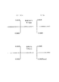
図5は、第1実施例におけるショット領域と部分露光領域と静止露光領域との関係を示す図である。図5に示すように、第1実施例では、Y方向に33mmでX方向に26mmの矩形状のショット領域51を、Y方向に33mmでX方向に13mmの大きさを有する2つの矩形状の部分露光領域51aと51bとに分割している。一方、投影光学系PLの半径7mmのイメージサークル内において、Y方向に5mmでX方向に13mmの矩形状の静止露光領域51cを設定している。
FIG. 5 is a diagram showing the relationship among the shot area, the partial exposure area, and the still exposure area in the first embodiment. As shown in FIG. 5, in the first embodiment, a
第1実施例では、たとえば6インチサイズのレチクルRを用いて、ショット領域51の1/2の大きさを有する第1部分露光領域51aへのスキャン露光を行う。第1部分露光領域51aへのスキャン露光に際しては、第1部分露光領域51aにおいて+Y方向側の端部位置から−Y方向側の端部位置まで静止露光領域51cが−Y方向へ移動するように、ウェハステージWSを、ひいてはウェハWを+Y方向へ移動させる。そして、ウェハWの+Y方向への移動に対応して、レチクルステージRSを、ひいてはレチクルRを−Y方向へ移動させる。
In the first embodiment, for example, a 6-inch reticle R is used to perform scan exposure on the first partial exposure region 51a having a size half that of the
次いで、レチクルRを交換することなく、ショット領域51の1/2の大きさを有する第2部分露光領域51bへのスキャン露光を行う。ただし、第2部分露光領域51bへのスキャン露光に先立って、静止露光領域51cが第1部分露光領域51aの−Y方向側の端部位置から第2部分露光領域51bの−Y方向側の端部位置まで+X方向へ移動するように、ウェハステージWSを、ひいてはウェハWを−X方向へ13mmだけステップ移動させる。そして、ウェハWの−X方向へのステップ移動に対応するように、レチクルステージRSを、ひいてはレチクルRを+X方向へ52mmだけステップ移動させる。
Next, scan exposure is performed on the second
第2部分露光領域51bへのスキャン露光に際しては、第2部分露光領域51bにおいて−Y方向側の端部位置から+Y方向側の端部位置まで静止露光領域51cが+Y方向へ移動するように、ウェハステージWSを、ひいてはウェハWを−Y方向へ移動させる。そして、ウェハWの−Y方向への移動に対応して、レチクルステージRSを、ひいてはレチクルRを+Y方向へ移動させる。なお、第1部分露光領域51aにおいて静止露光領域51cを−Y方向側の端部位置から+Y方向へ移動させるようにスキャン露光を開始してもよい。
At the time of scan exposure on the second
こうして、第1実施例では、投影光学系PLの大型化を招くことなく、2つの部分露光領域51aおよび51bへのスキャン露光により1つの既定サイズのショット領域51にレチクルパターンを転写するのに必要な所要の大きさの有効結像領域(イメージフィールド)を確保することができる。また、ウェハ(感光性基板)Wとの間の光路中に高屈折率の媒質として純水を介在させているので、大きな実効的な像側開口数を有する高解像な投影光学系PLを実現することができる。
Thus, in the first embodiment, it is necessary to transfer the reticle pattern to one predetermined size shot
その結果、第1実施例にかかる比較的小型の投影光学系PLを用いて、スティッチング方式にしたがって解像度の高い良好な投影露光を行うことができる。なお、スティッチング方式の露光装置のさらに詳細な構成および作用については、たとえば特許第3316754号公報や特開平8−330220号公報(及びこれに対応する米国特許第6295119号公報)などを参照することができる。 As a result, good projection exposure with high resolution can be performed according to the stitching method using the relatively small projection optical system PL according to the first embodiment. For more detailed configuration and operation of the stitching type exposure apparatus, refer to, for example, Japanese Patent No. 3316754, Japanese Patent Laid-Open No. 8-330220 (and corresponding US Pat. No. 6,295,119), and the like. Can do.
[第2実施例]
図6は、本実施形態の第2実施例にかかる投影光学系のレンズ構成を示す図である。図6を参照すると、第2実施例の投影光学系PLは、レチクル側から順に、平行平面板P1と、ウェハ側に非球面形状の凹面を向けた両凹レンズL1と、レチクル側に非球面形状の凹面を向けた負メニスカスレンズL2と、レチクル側に非球面形状の凹面を向けた正メニスカスレンズL3と、両凸レンズL4と、両凸レンズL5と、両凸レンズL6と、レチクル側に凸面を向けた正メニスカスレンズL7と、レチクル側に凸面を向けた正メニスカスレンズL8と、ウェハ側に非球面形状の凹面を向けた正メニスカスレンズL9と、レチクル側に凸面を向けた負メニスカスレンズL10と、レチクル側に非球面形状の凹面を向けた両凹レンズL11と、ウェハ側に非球面形状の凹面を向けた負メニスカスレンズL12と、ウェハ側に非球面形状の凹面を向けた両凹レンズL13と、レチクル側に非球面形状の凹面を向けた正メニスカスレンズL14と、レチクル側に凹面を向けた正メニスカスレンズL15と、レチクル側に凹面を向けた正メニスカスレンズL16と、レチクル側に凹面を向けた正メニスカスレンズL17と、両凸レンズL18と、レチクル側に凸面を向けた正メニスカスレンズL19と、ウェハ側に非球面形状の凹面を向けた正メニスカスレンズL20と、レチクル側に凸面を向けた正メニスカスレンズL21と、レチクル側に非球面形状の凸面を向けた平凸レンズL22(境界レンズLb)とにより構成されている。
[Second Embodiment]
FIG. 6 is a diagram showing a lens configuration of the projection optical system according to the second example of the present embodiment. Referring to FIG. 6, the projection optical system PL of the second embodiment includes, in order from the reticle side, a plane parallel plate P1, a biconcave lens L1 having an aspherical concave surface facing the wafer side, and an aspherical shape on the reticle side. Negative meniscus lens L2 with the concave surface facing the lens, positive meniscus lens L3 with the aspherical concave surface facing the reticle side, biconvex lens L4, biconvex lens L5, biconvex lens L6, and convex surface facing the reticle side A positive meniscus lens L7, a positive meniscus lens L8 having a convex surface facing the reticle, a positive meniscus lens L9 having an aspherical concave surface facing the wafer, a negative meniscus lens L10 having a convex surface facing the reticle, and a reticle A biconcave lens L11 with an aspherical concave surface facing the side, a negative meniscus lens L12 with an aspherical concave surface facing the wafer, and an aspherical shape on the wafer side A biconcave lens L13 having a concave surface, a positive meniscus lens L14 having an aspheric concave surface facing the reticle, a positive meniscus lens L15 having a concave surface facing the reticle, and a positive meniscus lens L16 having a concave surface facing the reticle A positive meniscus lens L17 having a concave surface facing the reticle, a biconvex lens L18, a positive meniscus lens L19 having a convex surface facing the reticle, a positive meniscus lens L20 having an aspheric concave surface facing the wafer, A positive meniscus lens L21 having a convex surface facing the reticle side and a plano-convex lens L22 (boundary lens Lb) having an aspherical convex surface facing the reticle side.
第2実施例においても第1実施例と同様に、境界レンズLbとしての平凸レンズL22とウェハWとの間の光路には、純水からなる媒質Lmが満たされている。また、レンズL21およびL22(Lb)が蛍石により形成され、その他のレンズ成分は石英により形成されている。次の表(2)に、第2実施例にかかる投影光学系PLの諸元の値を掲げる。 Also in the second example, as in the first example, the optical path between the plano-convex lens L22 as the boundary lens Lb and the wafer W is filled with a medium Lm made of pure water. The lenses L21 and L22 (Lb) are made of fluorite, and the other lens components are made of quartz. The following table (2) lists the values of the specifications of the projection optical system PL according to the second example.
表2
(主要諸元)
λ=193.306nm
β=−1/5
NA=1.2
φo=35mm
φi=7mm
(光学部材諸元)
面番号 r d n 光学部材
(レチクル面) 39.128
1 ∞ 4.242 1.5603261 (P1)
2 ∞ 3.103
3 -1120.724 14.000 1.5603261 (L1)
4* 147.421 31.308
5* -68.728 14.000 1.5603261 (L2)
6 -7403.000 12.107
7* -194.623 44.967 1.5603261 (L3)
8 -125.000 1.000
9 2000.000 37.115 1.5603261 (L4)
10 -400.000 1.000
11 758.189 58.479 1.5603261 (L5)
12 -351.098 25.253
13 741.225 60.000 1.5603261 (L6)
14 -1860.768 1.000
15 259.706 32.011 1.5603261 (L7)
16 469.076 1.000
17 160.278 38.364 1.5603261 (L8)
18 210.000 2.400
19 136.997 37.617 1.5603261 (L9)
20* 186.302 29.491
21 3292.401 60.000 1.5603261 (L10)
22 89.885 47.414
23* -201.039 14.000 1.5603261 (L11)
24 114.173 11.356
25 354.751 14.000 1.5603261 (L12)
26* 124.821 16.381
27 -1443.830 14.000 1.5603261 (L13)
28* 433.445 23.665
29* -670.291 36.731 1.5603261 (L14)
30 -131.312 1.000
31 -372.662 33.374 1.5603261 (L15)
32 -180.491 46.358
33 -432.487 40.119 1.5603261 (L16)
34 -215.706 28.798
35 -1240.698 60.000 1.5603261 (L17)
36 -306.986 1.000
37 466.924 44.386 1.5603261 (L18)
38 -677.350 1.000
39 135.740 51.010 1.5603261 (L19)
40 377.325 1.000
41 107.976 28.677 1.5603261 (L20)
42* 123.160 1.000
43 69.066 28.328 1.5014548 (L21)
44 60.410 2.205
45* 56.397 30.225 1.5014548 (L22:Lb)
46 ∞ 1.000 1.4360000 (Lm)
(ウェハ面)
(非球面データ)
4面
κ=0
C4=−2.60717×10⁻⁷ C6=2.19741×10⁻¹¹
C8=−4.76373×10⁻¹⁵ C10=5.01880×10⁻¹⁹
C12=2.67967×10⁻²² C14=−5.70993×10⁻²⁶
5面
κ=0
C4=−1.18693×10⁻⁷ C6=−2.14738×10⁻¹¹
C8=−4.39761×10⁻¹⁵ C10=−1.35408×10⁻¹⁹
C12=−3.19642×10⁻²² C14=5.45617×10⁻²⁶
7面
κ=0
C4=1.30657×10⁻⁷ C6=3.62264×10⁻¹²
C8=−7.14187×10⁻¹⁶ C10=−7.88242×10⁻²⁰
C12=1.76092×10⁻²³ C14=−8.51512×10⁻²⁸
20面
κ=0
C4=5.51155×10⁻⁸ C6=2.46578×10⁻¹³
C8=1.73270×10⁻¹⁷ C10=−2.08719×10⁻²²
C12=−2.45583×10⁻²⁶ C14=−1.29454×10⁻²⁹
23面
κ=0
C4=−3.21659×10⁻⁷ C6=5.36890×10⁻¹¹
C8=−1.57630×10⁻¹⁵ C10=−3.52310×10⁻¹⁸
C12=8.36219×10⁻²² C14=−6.28614×10⁻²⁶
26面
κ=0
C4=−1.62042×10⁻⁷ C6=1.76015×10⁻¹²
C8=1.01105×10⁻¹⁴ C10=−4.95645×10⁻¹⁸
C12=7.94312×10⁻²² C14=−4.79966×10⁻²⁶
28面
κ=0
C4=−7.20471×10⁻⁸ C6=3.09435×10⁻¹¹
C8=−9.06382×10⁻¹⁵ C10=1.26627×10⁻¹⁸
C12=−8.63134×10⁻²³ C14=2.34101×10⁻²⁷
29面
κ=0
C4=−1.47315×10⁻⁷ C6=1.28450×10⁻¹¹
C8=−1.38349×10⁻¹⁵ C10=1.12203×10⁻¹⁹
C12=−7.91413×10⁻²⁴ C14=3.35535×10⁻²⁸
42面
κ=0
C4=−1.93501×10⁻⁷ C6=5.46290×10⁻¹²
C8=2.10000×10⁻¹⁵ C10=−4.00324×10⁻¹⁹
C12=3.31300×10⁻²³ C14=−9.33193×10⁻²⁸
45面
κ=0
C4=−4.26845×10⁻⁷ C6=−7.56600×10⁻¹¹
C8=1.00727×10⁻¹⁴ C10=−2.62595×10⁻¹⁸
C12=−1.17646×10⁻²⁰ C14=4.62437×10⁻²⁴
(条件式対応値)
φmax=300mm
φo=35mm
(1)φmax/φo=8.571
Table 2
(Main specifications)
λ = 193.306 nm
β = -1 / 5
NA = 1.2
φo = 35mm
φi = 7mm
(Optical member specifications)
Surface number r dn optical member (reticle surface) 39.128
1 ∞ 4.242 1.5603261 (P1)
2 ∞ 3.103
3 -1120.724 14.000 1.5603261 (L1)
4 * 147.421 31.308
5 * -68.728 14.000 1.5603261 (L2)
6 -7403.000 12.107
7 * -194.623 44.967 1.5603261 (L3)
8 -125.000 1.000
9 2000.000 37.115 1.5603261 (L4)
10 -400.000 1.000
11 758.189 58.479 1.5603261 (L5)
12 -351.098 25.253
13 741.225 60.000 1.5603261 (L6)
14 -1860.768 1.000
15 259.706 32.011 1.5603261 (L7)
16 469.076 1.000
17 160.278 38.364 1.5603261 (L8)
18 210.000 2.400
19 136.997 37.617 1.5603261 (L9)
20 * 186.302 29.491
21 3292.401 60.000 1.5603261 (L10)
22 89.885 47.414
23 * -201.039 14.000 1.5603261 (L11)
24 114.173 11.356
25 354.751 14.000 1.5603261 (L12)
26 * 124.821 16.381
27 -1443.830 14.000 1.5603261 (L13)
28 * 433.445 23.665
29 * -670.291 36.731 1.5603261 (L14)
30 -131.312 1.000
31 -372.662 33.374 1.5603261 (L15)
32 -180.491 46.358
33 -432.487 40.119 1.5603261 (L16)
34 -215.706 28.798
35 -1240.698 60.000 1.5603261 (L17)
36 -306.986 1.000
37 466.924 44.386 1.5603261 (L18)
38 -677.350 1.000
39 135.740 51.010 1.5603261 (L19)
40 377.325 1.000
41 107.976 28.677 1.5603261 (L20)
42 * 123.160 1.000
43 69.066 28.328 1.5014548 (L21)
44 60.410 2.205
45 * 56.397 30.225 1.5014548 (L22: Lb)
46 ∞ 1.000 1.4360000 (Lm)
(Wafer surface)
(Aspheric data)
4 sides κ = 0
C 4 = −2.66071 × 10 −7 C 6 = 2.9741 × 10 −11
C 8 = −4.776373 × 10 −15 C 10 = 5.01880 × 10 −19
C 12 = 2.667967 × 10 −22 C 14 = −5.77093 × 10 −26
5 sides κ = 0
C 4 = −1.18693 × 10 −7 C 6 = −2.14738 × 10 −11
C 8 = −4.39761 × 10 −15 C 10 = −1.35408 × 10 −19
C 12 = −3.19642 × 10 −22 C 14 = 5.445617 × 10 −26
7 surfaces κ = 0
C 4 = 1.30657 × 10 −7 C 6 = 3.62264 × 10 −12
C 8 = −7.14187 × 10 −16 C 10 = −7.88822 × 10 −20
C 12 = 1.776092 × 10 −23 C 14 = −8.551512 × 10 −28
20 faces κ = 0
C 4 = 5.51155 × 10 −8 C 6 = 2.46578 × 10 −13
C 8 = 1.773270 × 10 −17 C 10 = −2.08719 × 10 −22
C 12 = −2.44553 × 10 −26 C 14 = −1.29454 × 10 −29
23 κ = 0
C 4 = −3.221659 × 10 −7 C 6 = 5.36890 × 10 −11
C 8 = −1.57630 × 10 −15 C 10 = −3.52310 × 10 −18
C 12 = 8.336219 × 10 −22 C 14 = −6.228614 × 10 −26
26 surfaces κ = 0
C 4 = −1.62042 × 10 −7 C 6 = 1.76015 × 10 −12
C 8 = 1.01105 × 10 −14 C 10 = −4.956645 × 10 −18
C 12 = 7.94312 × 10 −22 C 14 = −4.779966 × 10 −26
28 faces κ = 0
C 4 = −7.04711 × 10 −8 C 6 = 3.09435 × 10 −11
C 8 = −9.006382 × 10 −15 C 10 = 1.266627 × 10 −18
C 12 = −8.63134 × 10 −23 C 14 = 2.334101 × 10 −27
29 faces κ = 0
C 4 = −1.47315 × 10 −7 C 6 = 1.28450 × 10 −11
C 8 = −1.38349 × 10 −15 C 10 = 1.1203 × 10 −19
C 12 = −7.991413 × 10 −24 C 14 = 3.353535 × 10 −28
42 plane κ = 0
C 4 = −1.93501 × 10 −7 C 6 = 5.46290 × 10 −12
C 8 = 2.10000 × 10 −15 C 10 = −4.300324 × 10 −19
C 12 = 3.31300 × 10 −23 C 14 = −9.333193 × 10 −28
45 faces κ = 0
C 4 = −4.26845 × 10 −7 C 6 = −7.56600 × 10 −11
C 8 = 1.00727 × 10 −14 C 10 = −2.662595 × 10 −18
C 12 = −1.17646 × 10 −20 C 14 = 4.62437 × 10 −24
(Values for conditional expressions)
φmax = 300mm
φo = 35mm
(1) φmax / φo = 8.571
図7は、第2実施例における横収差を示す図である。収差図において、Yは像高を示している。図7の収差図から明らかなように、第2実施例では、投影倍率の大きさが1/5の投影光学系において、波長が193.306nmのArFエキシマレーザ光を用いて非常に大きな像側開口数(NA=1.2)を確保しているにもかかわらず、半径が7mmのイメージサークル内において収差が良好に補正されていることがわかる。 FIG. 7 is a diagram showing transverse aberration in the second example. In the aberration diagrams, Y indicates the image height. As is apparent from the aberration diagram of FIG. 7, in the second embodiment, a very large image side is obtained using ArF excimer laser light having a wavelength of 193.306 nm in a projection optical system having a projection magnification of 1/5. Although the numerical aperture (NA = 1.2) is secured, it can be seen that the aberration is well corrected in the image circle having a radius of 7 mm.
図8は、第2実施例におけるショット領域と部分露光領域と静止露光領域との関係を示す図である。図8に示すように、第2実施例では、Y方向に22mmでX方向に26mmの矩形状のショット領域52を、Y方向に22mmでX方向に13mmの大きさを有する2つの矩形状の部分露光領域52aと52bとに分割している。一方、投影光学系PLの半径7mmのイメージサークル内において、Y方向に5mmでX方向に13mmの矩形状の静止露光領域52cを設定している。
FIG. 8 is a diagram showing the relationship among the shot area, the partial exposure area, and the still exposure area in the second embodiment. As shown in FIG. 8, in the second embodiment, a
第2実施例では、たとえば6インチサイズのレチクルRを用いて、ショット領域52の1/2の大きさを有する第1部分露光領域52aへのスキャン露光を行う。第1部分露光領域52aへのスキャン露光に際しては、第1部分露光領域52aにおいて+Y方向側の端部位置から−Y方向側の端部位置まで静止露光領域52cが−Y方向へ移動するように、ウェハステージWSを、ひいてはウェハWを+Y方向へ移動させる。そして、ウェハWの+Y方向への移動に対応して、レチクルステージRSを、ひいてはレチクルRを−Y方向へ移動させる。
In the second embodiment, for example, a 6-inch reticle R is used to perform scan exposure on the first
次いで、レチクルRを交換することなく、ショット領域52の1/2の大きさを有する第2部分露光領域52bへのスキャン露光を行う。ただし、第2部分露光領域52bへのスキャン露光に先立って、静止露光領域52cが第1部分露光領域52aの−Y方向側の端部位置から第2部分露光領域52bの−Y方向側の端部位置まで+X方向へ移動するように、ウェハステージWSを、ひいてはウェハWを−X方向へ13mmだけステップ移動させる。そして、ウェハWの−X方向へのステップ移動に対応するように、レチクルステージRSを、ひいてはレチクルRを+X方向へ65mmだけステップ移動させる。
Next, scan exposure is performed on the second
第2部分露光領域52bへのスキャン露光に際しては、第2部分露光領域52bにおいて−Y方向側の端部位置から+Y方向側の端部位置まで静止露光領域52cが+Y方向へ移動するように、ウェハステージWSを、ひいてはウェハWを−Y方向へ移動させる。そして、ウェハWの−Y方向への移動に対応して、レチクルステージRSを、ひいてはレチクルRを+Y方向へ移動させる。なお、第1部分露光領域52aにおいて静止露光領域52cを−Y方向側の端部位置から+Y方向へ移動させるようにスキャン露光を開始してもよい。
At the time of scan exposure to the second
こうして、第2実施例においても、投影光学系PLの大型化を招くことなく、2つの部分露光領域52aおよび52bへのスキャン露光により1つの既定サイズのショット領域52にレチクルパターンを転写するのに必要な所要の大きさの有効結像領域(イメージフィールド)を確保することができる。また、ウェハ(感光性基板)Wとの間の光路中に高屈折率の媒質として純水を介在させているので、大きな実効的な像側開口数を有する高解像な投影光学系PLを実現することができる。その結果、第2実施例にかかる比較的小型の投影光学系PLを用いて、スティッチング方式にしたがって解像度の高い良好な投影露光を行うことができる。
Thus, also in the second embodiment, the reticle pattern is transferred to one
[第3実施例]
図9は、本実施形態の第2実施例にかかる投影光学系のレンズ構成を示す図である。図9を参照すると、第2実施例の投影光学系PLは、レチクル側から順に、平行平面板P1と、ウェハ側に非球面形状の凹面を向けた両凹レンズL1と、レチクル側に非球面形状の凹面を向けた負メニスカスレンズL2と、レチクル側に非球面形状の凹面を向けた正メニスカスレンズL3と、両凸レンズL4と、両凸レンズL5と、両凸レンズL6と、レチクル側に凸面を向けた正メニスカスレンズL7と、レチクル側に凸面を向けた正メニスカスレンズL8と、ウェハ側に非球面形状の凹面を向けた正メニスカスレンズL9と、レチクル側に凸面を向けた負メニスカスレンズL10と、レチクル側に非球面形状の凹面を向けた両凹レンズL11と、ウェハ側に非球面形状の凹面を向けた負メニスカスレンズL12と、ウェハ側に非球面形状の凹面を向けた両凹レンズL13と、レチクル側に非球面形状の凹面を向けた正メニスカスレンズL14と、レチクル側に凹面を向けた正メニスカスレンズL15と、レチクル側に凹面を向けた正メニスカスレンズL16と、レチクル側に凹面を向けた正メニスカスレンズL17と、両凸レンズL18と、レチクル側に凸面を向けた正メニスカスレンズL19と、ウェハ側に非球面形状の凹面を向けた正メニスカスレンズL20と、レチクル側に凸面を向けた正メニスカスレンズL21と、レチクル側に非球面形状の凸面を向けた平凸レンズL22(境界レンズLb)とにより構成されている。
[Third embodiment]
FIG. 9 is a diagram showing a lens configuration of the projection optical system according to the second example of the present embodiment. Referring to FIG. 9, the projection optical system PL of the second embodiment includes, in order from the reticle side, a plane parallel plate P1, a biconcave lens L1 having an aspherical concave surface facing the wafer side, and an aspherical shape on the reticle side. Negative meniscus lens L2 with the concave surface facing the lens, positive meniscus lens L3 with the aspherical concave surface facing the reticle side, biconvex lens L4, biconvex lens L5, biconvex lens L6, and convex surface facing the reticle side A positive meniscus lens L7, a positive meniscus lens L8 having a convex surface facing the reticle, a positive meniscus lens L9 having an aspherical concave surface facing the wafer, a negative meniscus lens L10 having a convex surface facing the reticle, and a reticle A biconcave lens L11 with an aspherical concave surface facing the side, a negative meniscus lens L12 with an aspherical concave surface facing the wafer, and an aspherical shape on the wafer side A biconcave lens L13 having a concave surface, a positive meniscus lens L14 having an aspheric concave surface facing the reticle, a positive meniscus lens L15 having a concave surface facing the reticle, and a positive meniscus lens L16 having a concave surface facing the reticle A positive meniscus lens L17 having a concave surface facing the reticle, a biconvex lens L18, a positive meniscus lens L19 having a convex surface facing the reticle, a positive meniscus lens L20 having an aspheric concave surface facing the wafer, A positive meniscus lens L21 having a convex surface facing the reticle side and a plano-convex lens L22 (boundary lens Lb) having an aspherical convex surface facing the reticle side.
第3実施例においても第1実施例および第2実施例と同様に、境界レンズLbとしての平凸レンズL22とウェハWとの間の光路には、純水からなる媒質Lmが満たされている。また、レンズL21およびL22(Lb)が蛍石により形成され、その他のレンズ成分は石英により形成されている。次の表(3)に、第3実施例にかかる投影光学系PLの諸元の値を掲げる。 In the third embodiment, similarly to the first and second embodiments, the optical path between the plano-convex lens L22 as the boundary lens Lb and the wafer W is filled with a medium Lm made of pure water. The lenses L21 and L22 (Lb) are made of fluorite, and the other lens components are made of quartz. The following table (3) lists the values of the specifications of the projection optical system PL according to the third example.
表3
(主要諸元)
λ=193.306nm
β=−1/4
NA=1.2
φo=52.8mm
φi=13.2mm
(光学部材諸元)
面番号 r d n 光学部材
(レチクル面) 41.959
1 ∞ 8.000 1.5603261 (P1)
2 ∞ 5.852
3 -2113.365 14.000 1.5603261 (L1)
4* 221.428 46.651
5* -110.397 14.003 1.5603261 (L2)
6 -2038.116 14.952
7* -268.471 60.000 1.5603261 (L3)
8 -163.574 2.204
9 787.073 47.564 1.5603261 (L4)
10 -1199.653 69.409
11 1481.028 56.029 1.5603261 (L5)
12 -900.000 1.000
13 889.835 59.955 1.5603261 (L6)
14 -1400.966 1.000
15 399.864 48.700 1.5603261 (L7)
16 886.381 1.000
17 263.334 41.519 1.5603261 (L8)
18 353.549 1.000
19 184.590 61.940 1.5603261 (L9)
20* 302.692 40.787
21 2236.773 35.719 1.5603261 (L10)
22 133.772 91.786
23* -236.082 14.006 1.5603261 (L11)
24 222.881 17.448
25 518.618 14.018 1.5603261 (L12)
26* 223.081 29.074
27 -2658.035 17.547 1.5603261 (L13)
28* 817.034 43.358
29* -918.788 60.000 1.5603261 (L14)
30 -231.616 1.000
31 -870.224 53.941 1.5603261 (L15)
32 -321.031 102.844
33 -835.483 60.543 1.5603261 (L16)
34 -380.671 47.589
35 -3293.468 59.159 1.5603261 (L17)
36 -571.474 1.001
37 951.991 65.054 1.5603261 (L18)
38 -1182.645 1.001
39 252.145 79.173 1.5603261 (L19)
40 774.296 1.001
41 203.245 44.417 1.5603261 (L20)
42* 277.487 1.000
43 111.053 49.176 1.5014548 (L21)
44 73.419 11.556
45* 82.853 60.000 1.5014548 (L22:Lb)
46 ∞ 1.000 1.4360000 (Lm)
(ウェハ面)
(非球面データ)
4面
κ=0
C4=−8.42204×10⁻⁸ C6=2.80152×10⁻¹²
C8=−2.22208×10⁻¹⁶ C10=4.92545×10⁻²¹
C12=1.55578×10⁻²⁴ C14=−1.36027×10⁻²⁸
5面
κ=0
C4=−1.78733×10⁻⁸ C6=−5.09565×10⁻¹²
C8=−1.32647×10⁻¹⁶ C10=−1.78491×10⁻²⁰
C12=−1.09697×10⁻²⁴ C14=−2.65434×10⁻²⁸
7面
κ=0
C4=3.79075×10⁻⁸ C6=1.98975×10⁻¹²
C8=−1.07206×10⁻¹⁶ C10=−4.95516×10⁻²¹
C12=5.25305×10⁻²⁵ C14=−1.31079×10⁻²⁹
20面
κ=0
C4=1.28527×10⁻⁸ C6=−1.50420×10⁻¹³
C8=−2.38430×10⁻¹⁸ C10=−4.55067×10⁻²⁴
C12=−2.97021×10⁻²⁷ C14=−1.25981×10⁻³²
23面
κ=0
C4=−6.27820×10⁻⁸ C6=4.17470×10⁻¹²
C8=−1.61854×10⁻¹⁶ C10=−7.84123×10⁻²¹
C12=8.94065×10⁻²⁵ C14=−2.28944×10⁻²⁹
26面
κ=0
C4=−2.77048×10⁻⁸ C6=6.64882×10⁻¹³
C8=5.96372×10⁻¹⁷ C10=−1.90851×10⁻²⁰
C12=1.14332×10⁻²⁴ C14=−2.37083×10⁻²⁹
28面
κ=0
C4=−7.27736×10⁻⁹ C6=1.31053×10⁻¹²
C8=−1.34460×10⁻¹⁶ C10=5.97618×10⁻²¹
C12=−1.10021×10⁻²⁵ C14=3.18721×10⁻³¹
29面
κ=0
C4=−2.41934×10⁻⁸ C6=5.15680×10⁻¹³
C8=−1.83503×10⁻¹⁷ C10=4.25022×10⁻²²
C12=−1.00631×10⁻²⁶ C14=1.53135×10⁻³¹
42面
κ=0
C4=−1.83510×10⁻⁸ C6=1.51025×10⁻¹³
C8=1.31925×10⁻¹⁷ C10=−5.95100×10⁻²²
C12=1.20766×10⁻²⁶ C14=−8.72208×10⁻³²
45面
κ=0
C4=2.18842×10⁻⁸ C6=1.04930×10⁻¹²
C8=4.59769×10⁻¹⁶ C10=−1.35609×10⁻¹⁹
C12=4.22209×10⁻²³ C14=−7.03010×10⁻²⁷
(条件式対応値)
φmax=500mm
φo=52.8mm
(1)φmax/φo=9.470
Table 3
(Main specifications)
λ = 193.306 nm
β = -1 / 4
NA = 1.2
φo = 52.8mm
φi = 13.2mm
(Optical member specifications)
Surface number r dn optical member (reticle surface) 41.959
1 ∞ 8.000 1.5603261 (P1)
2 ∞ 5.852
3 -2113.365 14.000 1.5603261 (L1)
4 * 221.428 46.651
5 * -110.397 14.003 1.5603261 (L2)
6 -2038.116 14.952
7 * -268.471 60.000 1.5603261 (L3)
8 -163.574 2.204
9 787.073 47.564 1.5603261 (L4)
10 -1199.653 69.409
11 1481.028 56.029 1.5603261 (L5)
12 -900.000 1.000
13 889.835 59.955 1.5603261 (L6)
14 -1400.966 1.000
15 399.864 48.700 1.5603261 (L7)
16 886.381 1.000
17 263.334 41.519 1.5603261 (L8)
18 353.549 1.000
19 184.590 61.940 1.5603261 (L9)
20 * 302.692 40.787
21 2236.773 35.719 1.5603261 (L10)
22 133.772 91.786
23 * -236.082 14.006 1.5603261 (L11)
24 222.881 17.448
25 518.618 14.018 1.5603261 (L12)
26 * 223.081 29.074
27 -2658.035 17.547 1.5603261 (L13)
28 * 817.034 43.358
29 * -918.788 60.000 1.5603261 (L14)
30 -231.616 1.000
31 -870.224 53.941 1.5603261 (L15)
32 -321.031 102.844
33 -835.483 60.543 1.5603261 (L16)
34 -380.671 47.589
35 -3293.468 59.159 1.5603261 (L17)
36 -571.474 1.001
37 951.991 65.054 1.5603261 (L18)
38 -1182.645 1.001
39 252.145 79.173 1.5603261 (L19)
40 774.296 1.001
41 203.245 44.417 1.5603261 (L20)
42 * 277.487 1.000
43 111.053 49.176 1.5014548 (L21)
44 73.419 11.556
45 * 82.853 60.000 1.5014548 (L22: Lb)
46 ∞ 1.000 1.4360000 (Lm)
(Wafer surface)
(Aspheric data)
4 sides κ = 0
C 4 = −8.42204 × 10 −8 C 6 = 2.80152 × 10 −12
C 8 = −2.22208 × 10 −16 C 10 = 4.992545 × 10 −21
C 12 = 1.55578 × 10 −24 C 14 = −1.36027 × 10 −28
5 sides κ = 0
C 4 = -1.78733 × 10 −8 C 6 = −5.09565 × 10 −12
C 8 = −1.32647 × 10 −16 C 10 = −1.78491 × 10 −20
C 12 = −1.09697 × 10 −24 C 14 = −2.665434 × 10 −28
7 surfaces κ = 0
C 4 = 3.77905 × 10 −8 C 6 = 1.98775 × 10 −12
C 8 = −1.07206 × 10 −16 C 10 = −4.95516 × 10 −21
C 12 = 5.225305 × 10 −25 C 14 = −1.31079 × 10 −29
20 faces κ = 0
C 4 = 1.28527 × 10 −8 C 6 = −1.54020 × 10 −13
C 8 = −2.38430 × 10 −18 C 10 = −4.555067 × 10 −24
C 12 = -2.97021 × 10 −27 C 14 = −1.25981 × 10 −32
23 κ = 0
C 4 = −6.28820 × 10 −8 C 6 = 4.17470 × 10 −12
C 8 = −1.61854 × 10 −16 C 10 = −7.84123 × 10 −21
C 12 = 8.994065 × 10 −25 C 14 = −2.289944 × 10 −29
26 surfaces κ = 0
C 4 = −2.77704 × 10 −8 C 6 = 6.66482 × 10 −13
C 8 = 5.996372 × 10 −17 C 10 = −1.90885 × 10 −20
C 12 = 1.114332 × 10 −24 C 14 = −2.37083 × 10 −29
28 faces κ = 0
C 4 = −7.227736 × 10 −9 C 6 = 1.31053 × 10 −12
C 8 = −1.34460 × 10 −16 C 10 = 5.997618 × 10 −21
C 12 = −1.10021 × 10 −25 C 14 = 3.187721 × 10 −31
29 faces κ = 0
C 4 = −2.419434 × 10 −8 C 6 = 5.16680 × 10 −13
C 8 = −1.83503 × 10 −17 C 10 = 4.225022 × 10 −22
C 12 = -1.00631 × 10 −26 C 14 = 1.53135 × 10 −31
42 plane κ = 0
C 4 = −1.83510 × 10 −8 C 6 = 1.51025 × 10 −13
C 8 = 1.31925 × 10 −17 C 10 = −5.95 100 × 10 −22
C 12 = 1.20766 × 10 −26 C 14 = −8.772208 × 10 −32
45 faces κ = 0
C 4 = 2.18842 × 10 −8 C 6 = 1.04930 × 10 −12
C 8 = 4.59769 × 10 −16 C 10 = −1.35609 × 10 −19
C 12 = 4.222209 × 10 −23 C 14 = −7.03010 × 10 −27
(Values for conditional expressions)
φmax = 500mm
φo = 52.8mm
(1) φmax / φo = 9.470
図10は、第3実施例における横収差を示す図である。収差図において、Yは像高を示している。図10の収差図から明らかなように、第3実施例では、投影倍率の大きさが1/4の投影光学系において、波長が193.306nmのArFエキシマレーザ光を用いて非常に大きな像側開口数(NA=1.2)を確保しているにもかかわらず、半径が13.2mmのイメージサークル内において収差が良好に補正されていることがわかる。 FIG. 10 is a diagram showing transverse aberration in the third example. In the aberration diagrams, Y indicates the image height. As is apparent from the aberration diagram of FIG. 10, in the third example, a very large image side is obtained using ArF excimer laser light having a wavelength of 193.306 nm in a projection optical system having a projection magnification of 1/4. Although the numerical aperture (NA = 1.2) is secured, it can be seen that the aberration is well corrected in the image circle having a radius of 13.2 mm.
図11は、第3実施例におけるショット領域と静止露光領域との関係を示す図である。図11に示すように、第3実施例では、Y方向に33mmでX方向に25mmの矩形状のショット領域53に対して、投影光学系PLの半径13.2mmのイメージサークル内において、Y方向に8mmでX方向に25mmの矩形状の静止露光領域53cを設定している。第3実施例では、たとえば6インチサイズのレチクルRを用いて、ショット領域53へのスキャン露光を行う。
FIG. 11 is a diagram showing a relationship between a shot area and a static exposure area in the third embodiment. As shown in FIG. 11, in the third embodiment, a
ショット領域53へのスキャン露光に際しては、ショット領域53において+Y方向側の端部位置から−Y方向側の端部位置まで静止露光領域53cが−Y方向へ移動するように、ウェハステージWSを、ひいてはウェハWを+Y方向へ移動させる。そして、ウェハWの+Y方向への移動に対応して、レチクルステージRSを、ひいてはレチクルRを−Y方向へ移動させる。なお、ショット領域53において静止露光領域53cを−Y方向側の端部位置から+Y方向へ移動させるようにスキャン露光を開始してもよい。
At the time of scan exposure to the
こうして、第3実施例では、投影光学系PLの大型化を招くことなく、一回のスキャン露光により1つの既定サイズのショット領域53にレチクルパターンを転写するのに必要な所要の大きさの有効結像領域(イメージフィールド)を確保することができる。また、ウェハ(感光性基板)Wとの間の光路中に高屈折率の媒質として純水を介在させているので、大きな実効的な像側開口数を有する高解像な投影光学系PLを実現することができる。
Thus, in the third embodiment, the required size required to transfer the reticle pattern to one
なお、上述の第1実施例および第2実施例では、1つのショット領域を2つの部分露光領域に分割し、第1部分露光領域へのスキャン方向と第2部分露光領域へのスキャン方向とを逆に設定している。しかしながら、これに限定されることなく、1つのショット領域内における第1部分露光領域へのスキャン方向と第2部分露光領域へのスキャン方向とを同じに設定することもできる。この場合、各ショット領域について第1部分露光領域へのスキャン露光を順次行った後に、各ショット領域について第2部分露光領域へのスキャン露光を順次行う。あるいは、1つのショット領域内における第1部分露光領域へのスキャン露光と第2部分露光領域へのスキャン露光とを連続的に行いつつ、各ショット領域への露光を順次行う。 In the first and second embodiments described above, one shot area is divided into two partial exposure areas, and the scan direction to the first partial exposure area and the scan direction to the second partial exposure area are determined. The setting is reversed. However, the present invention is not limited to this, and the scan direction to the first partial exposure area and the scan direction to the second partial exposure area in one shot area can be set to be the same. In this case, after the scan exposure to the first partial exposure region is sequentially performed for each shot region, the scan exposure to the second partial exposure region is sequentially performed for each shot region. Alternatively, the exposure to each shot area is sequentially performed while continuously performing the scan exposure to the first partial exposure area and the scan exposure to the second partial exposure area in one shot area.
また、上述の第1実施例および第2実施例では、1つのショット領域を2つの部分露光領域に等分しているが、2つの部分露光領域を部分的に重複させて、いわゆる一部重複露光を行うこともできる。また、上述の第1実施例および第2実施例では、1つのショット領域を2つの部分露光領域に分割し、各部分露光領域に対するスキャン露光を1回ずつ行っているが、少なくとも1つの部分露光領域に対して二重露光を行うこともできる。 In the first and second embodiments described above, one shot area is equally divided into two partial exposure areas, but the two partial exposure areas are partially overlapped, so-called partial overlap. Exposure can also be performed. In the first and second embodiments described above, one shot area is divided into two partial exposure areas, and each partial exposure area is scanned once. However, at least one partial exposure is performed. Double exposure can also be performed on the area.
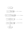
上述の実施形態の露光装置では、照明装置によってレチクル(マスク)を照明し(照明工程)、投影光学系を用いてマスクに形成された転写用のパターンを感光性基板に露光する(露光工程)ことにより、マイクロデバイス(半導体素子、撮像素子、液晶表示素子、薄膜磁気ヘッド等)を製造することができる。以下、本実施形態の露光装置を用いて感光性基板としてのウェハ等に所定の回路パターンを形成することによって、マイクロデバイスとしての半導体デバイスを得る際の手法の一例につき図12のフローチャートを参照して説明する。 In the exposure apparatus of the above-described embodiment, the reticle (mask) is illuminated by the illumination device (illumination process), and the transfer pattern formed on the mask is exposed to the photosensitive substrate using the projection optical system (exposure process). Thus, a micro device (semiconductor element, imaging element, liquid crystal display element, thin film magnetic head, etc.) can be manufactured. Hereinafter, referring to the flowchart of FIG. 12 for an example of a technique for obtaining a semiconductor device as a micro device by forming a predetermined circuit pattern on a wafer or the like as a photosensitive substrate using the exposure apparatus of this embodiment. I will explain.
先ず、図12のステップ301において、1ロットのウェハ上に金属膜が蒸着される。次のステップ302において、その1ロットのウェハ上の金属膜上にフォトレジストが塗布される。その後、ステップ303において、本実施形態の露光装置を用いて、マスク上のパターンの像がその投影光学系を介して、その1ロットのウェハ上の各ショット領域に順次露光転写される。その後、ステップ304において、その1ロットのウェハ上のフォトレジストの現像が行われた後、ステップ305において、その1ロットのウェハ上でレジストパターンをマスクとしてエッチングを行うことによって、マスク上のパターンに対応する回路パターンが、各ウェハ上の各ショット領域に形成される。 First, in step 301 of FIG. 12, a metal film is deposited on one lot of wafers. In the next step 302, a photoresist is applied on the metal film on the one lot of wafers. Thereafter, in step 303, using the exposure apparatus of the present embodiment, the image of the pattern on the mask is sequentially exposed and transferred to each shot area on the wafer of one lot via the projection optical system. Thereafter, in step 304, the photoresist on the one lot of wafers is developed, and in step 305, the resist pattern is etched on the one lot of wafers to form a pattern on the mask. Corresponding circuit patterns are formed in each shot area on each wafer.
その後、更に上のレイヤの回路パターンの形成等を行うことによって、半導体素子等のデバイスが製造される。上述の半導体デバイス製造方法によれば、極めて微細な回路パターンを有する半導体デバイスをスループット良く得ることができる。なお、ステップ301〜ステップ305では、ウェハ上に金属を蒸着し、その金属膜上にレジストを塗布、そして露光、現像、エッチングの各工程を行っているが、これらの工程に先立って、ウェハ上にシリコンの酸化膜を形成後、そのシリコンの酸化膜上にレジストを塗布、そして露光、現像、エッチング等の各工程を行っても良いことはいうまでもない。 Thereafter, a device pattern such as a semiconductor element is manufactured by forming a circuit pattern of an upper layer. According to the semiconductor device manufacturing method described above, a semiconductor device having an extremely fine circuit pattern can be obtained with high throughput. In steps 301 to 305, a metal is deposited on the wafer, a resist is applied on the metal film, and exposure, development, and etching processes are performed. Prior to these processes, on the wafer. It is needless to say that after forming a silicon oxide film, a resist may be applied on the silicon oxide film, and steps such as exposure, development, and etching may be performed.
また、本実施形態の露光装置では、プレート(ガラス基板)上に所定のパターン(回路パターン、電極パターン等)を形成することによって、マイクロデバイスとしての液晶表示素子を得ることもできる。以下、図13のフローチャートを参照して、このときの手法の一例につき説明する。図13において、パターン形成工程401では、本実施形態の露光装置を用いてマスクのパターンを感光性基板(レジストが塗布されたガラス基板等)に転写露光する、所謂光リソグラフィ工程が実行される。この光リソグラフィー工程によって、感光性基板上には多数の電極等を含む所定パターンが形成される。その後、露光された基板は、現像工程、エッチング工程、レジスト剥離工程等の各工程を経ることによって、基板上に所定のパターンが形成され、次のカラーフィルター形成工程402へ移行する。 In the exposure apparatus of this embodiment, a liquid crystal display element as a micro device can be obtained by forming a predetermined pattern (circuit pattern, electrode pattern, etc.) on a plate (glass substrate). Hereinafter, an example of the technique at this time will be described with reference to the flowchart of FIG. In FIG. 13, in a pattern forming process 401, a so-called photolithography process is performed in which a mask pattern is transferred and exposed to a photosensitive substrate (such as a glass substrate coated with a resist) using the exposure apparatus of the present embodiment. By this photolithography process, a predetermined pattern including a large number of electrodes and the like is formed on the photosensitive substrate. Thereafter, the exposed substrate undergoes steps such as a developing step, an etching step, and a resist stripping step, whereby a predetermined pattern is formed on the substrate, and the process proceeds to the next color filter forming step 402.
次に、カラーフィルター形成工程402では、R(Red)、G(Green)、B(Blue)に対応した3つのドットの組がマトリックス状に多数配列されたり、またはR、G、Bの3本のストライプのフィルターの組を複数水平走査線方向に配列されたりしたカラーフィルターを形成する。そして、カラーフィルター形成工程402の後に、セル組み立て工程403が実行される。セル組み立て工程403では、パターン形成工程401にて得られた所定パターンを有する基板、およびカラーフィルター形成工程402にて得られたカラーフィルター等を用いて液晶パネル(液晶セル)を組み立てる。 Next, in the color filter forming step 402, a large number of sets of three dots corresponding to R (Red), G (Green), and B (Blue) are arranged in a matrix or three of R, G, and B A color filter is formed by arranging a plurality of stripe filter sets in the horizontal scanning line direction. Then, after the color filter forming step 402, a cell assembly step 403 is executed. In the cell assembly step 403, a liquid crystal panel (liquid crystal cell) is assembled using the substrate having the predetermined pattern obtained in the pattern formation step 401, the color filter obtained in the color filter formation step 402, and the like.
セル組み立て工程403では、例えば、パターン形成工程401にて得られた所定パターンを有する基板とカラーフィルター形成工程402にて得られたカラーフィルターとの間に液晶を注入して、液晶パネル(液晶セル)を製造する。その後、モジュール組み立て工程404にて、組み立てられた液晶パネル(液晶セル)の表示動作を行わせる電気回路、バックライト等の各部品を取り付けて液晶表示素子として完成させる。上述の液晶表示素子の製造方法によれば、極めて微細な回路パターンを有する液晶表示素子をスループット良く得ることができる。 In the cell assembly step 403, for example, liquid crystal is injected between the substrate having the predetermined pattern obtained in the pattern formation step 401 and the color filter obtained in the color filter formation step 402, and a liquid crystal panel (liquid crystal cell) is obtained. ). Thereafter, in a module assembling step 404, components such as an electric circuit and a backlight for performing a display operation of the assembled liquid crystal panel (liquid crystal cell) are attached to complete a liquid crystal display element. According to the above-described method for manufacturing a liquid crystal display element, a liquid crystal display element having an extremely fine circuit pattern can be obtained with high throughput.
なお、上述の実施形態では、ArFエキシマレーザ光源を用いているが、これに限定されることなく、他の適当な光源を用いることもできる。また、上述の実施形態では、露光装置に搭載される投影光学系に対して本発明を適用しているが、これに限定されることなく、他の一般的な投影光学系に対して本発明を適用することもできる。 In the above-described embodiment, the ArF excimer laser light source is used. However, the present invention is not limited to this, and other appropriate light sources can also be used. In the above-described embodiment, the present invention is applied to the projection optical system mounted on the exposure apparatus. However, the present invention is not limited to this, and the present invention is applied to other general projection optical systems. Can also be applied.
Lb 境界レンズ
Lm 媒質(純水)
Li 各レンズ成分
100 レーザ光源
IL 照明光学系
R レチクル
RS レチクルステージ
PL 投影光学系
W ウェハ
WS ウェハステージ
Lb Boundary lens Lm Medium (pure water)
Li Each
Claims (12)
前記第1面における最大物高をφoとし、前記投影光学系中のすべてのレンズの有効径のうちの最大となる有効径の値をφmaxとするとき、
6.6<φmax/φo<12
の条件を満足することを特徴とする投影光学系。 In a projection optical system for forming a reduced image of the first surface on the second surface,
When the maximum object height on the first surface is φo, and the maximum effective diameter value of all the effective diameters of the lenses in the projection optical system is φmax,
6.6 <φmax / φo <12
A projection optical system characterized by satisfying the following conditions.
前記露光工程は、前記部分露光領域へ投影露光する部分露光工程を少なくとも2つ有し、
前記部分露光工程では、前記投影光学系に対して前記マスクおよび前記感光性基板を相対移動させつつ前記部分露光領域への走査露光を行うことを特徴とする請求項4に記載の露光方法。 In the exposure step, projection exposure is performed on one shot area including two partial exposure areas,
The exposure step includes at least two partial exposure steps of projecting and exposing to the partial exposure region,
5. The exposure method according to claim 4, wherein in the partial exposure step, scanning exposure is performed on the partial exposure region while moving the mask and the photosensitive substrate relative to the projection optical system.
前記露光工程は、前記複数のショット領域中の所定の前記部分露光領域へ投影露光する第1回目の部分露光工程と、前記複数のショット領域中の別の前記部分露光領域へ投影露光する第2回目の部分露光工程とを有することを特徴とする請求項5または7に記載の露光方法。 In the exposure step, projection exposure is performed on a plurality of shot areas,
The exposure step includes a first partial exposure step in which projection exposure is performed on the predetermined partial exposure region in the plurality of shot regions, and a second projection exposure is performed on another partial exposure region in the plurality of shot regions. The exposure method according to claim 5, further comprising a second partial exposure step.
前記マスクを支持して前記所定の方向とほぼ直交する方向にステップ移動させるためのマスクステージをさらに備えていることを特徴とする請求項11に記載の露光装置。 Scanning exposure to the photosensitive substrate while moving the mask and the photosensitive substrate in a predetermined direction with respect to the projection optical system,
The exposure apparatus according to claim 11, further comprising a mask stage for supporting the mask and moving it stepwise in a direction substantially orthogonal to the predetermined direction.
Priority Applications (1)
| Application Number | Priority Date | Filing Date | Title |
|---|---|---|---|
| JP2004065375A JP2005257740A (en) | 2004-03-09 | 2004-03-09 | Projection optical system, exposing device, and exposure method |
Applications Claiming Priority (1)
| Application Number | Priority Date | Filing Date | Title |
|---|---|---|---|
| JP2004065375A JP2005257740A (en) | 2004-03-09 | 2004-03-09 | Projection optical system, exposing device, and exposure method |
Publications (2)
| Publication Number | Publication Date |
|---|---|
| JP2005257740A true JP2005257740A (en) | 2005-09-22 |
| JP2005257740A5 JP2005257740A5 (en) | 2008-02-28 |
Family
ID=35083560
Family Applications (1)
| Application Number | Title | Priority Date | Filing Date |
|---|---|---|---|
| JP2004065375A Withdrawn JP2005257740A (en) | 2004-03-09 | 2004-03-09 | Projection optical system, exposing device, and exposure method |
Country Status (1)
| Country | Link |
|---|---|
| JP (1) | JP2005257740A (en) |
Cited By (13)
| Publication number | Priority date | Publication date | Assignee | Title |
|---|---|---|---|---|
| US7869122B2 (en) | 2004-01-14 | 2011-01-11 | Carl Zeiss Smt Ag | Catadioptric projection objective |
| US8199400B2 (en) | 2004-01-14 | 2012-06-12 | Carl Zeiss Smt Gmbh | Catadioptric projection objective |
| US20130271945A1 (en) | 2004-02-06 | 2013-10-17 | Nikon Corporation | Polarization-modulating element, illumination optical apparatus, exposure apparatus, and exposure method |
| US8913316B2 (en) | 2004-05-17 | 2014-12-16 | Carl Zeiss Smt Gmbh | Catadioptric projection objective with intermediate images |
| US9341954B2 (en) | 2007-10-24 | 2016-05-17 | Nikon Corporation | Optical unit, illumination optical apparatus, exposure apparatus, and device manufacturing method |
| US9423698B2 (en) | 2003-10-28 | 2016-08-23 | Nikon Corporation | Illumination optical apparatus and projection exposure apparatus |
| US9678437B2 (en) | 2003-04-09 | 2017-06-13 | Nikon Corporation | Illumination optical apparatus having distribution changing member to change light amount and polarization member to set polarization in circumference direction |
| US9678332B2 (en) | 2007-11-06 | 2017-06-13 | Nikon Corporation | Illumination apparatus, illumination method, exposure apparatus, and device manufacturing method |
| US9885872B2 (en) | 2003-11-20 | 2018-02-06 | Nikon Corporation | Illumination optical apparatus, exposure apparatus, and exposure method with optical integrator and polarization member that changes polarization state of light |
| US9891539B2 (en) | 2005-05-12 | 2018-02-13 | Nikon Corporation | Projection optical system, exposure apparatus, and exposure method |
| US10101666B2 (en) | 2007-10-12 | 2018-10-16 | Nikon Corporation | Illumination optical apparatus, exposure apparatus, and device manufacturing method |
| US10451973B2 (en) | 2005-05-03 | 2019-10-22 | Asml Netherlands B.V. | Lithographic apparatus and device manufacturing method |
| US10495981B2 (en) | 2005-03-04 | 2019-12-03 | Asml Netherlands B.V. | Lithographic apparatus and device manufacturing method |
-
2004
- 2004-03-09 JP JP2004065375A patent/JP2005257740A/en not_active Withdrawn
Cited By (35)
| Publication number | Priority date | Publication date | Assignee | Title |
|---|---|---|---|---|
| US9678437B2 (en) | 2003-04-09 | 2017-06-13 | Nikon Corporation | Illumination optical apparatus having distribution changing member to change light amount and polarization member to set polarization in circumference direction |
| US9885959B2 (en) | 2003-04-09 | 2018-02-06 | Nikon Corporation | Illumination optical apparatus having deflecting member, lens, polarization member to set polarization in circumference direction, and optical integrator |
| US9423698B2 (en) | 2003-10-28 | 2016-08-23 | Nikon Corporation | Illumination optical apparatus and projection exposure apparatus |
| US9760014B2 (en) | 2003-10-28 | 2017-09-12 | Nikon Corporation | Illumination optical apparatus and projection exposure apparatus |
| US10281632B2 (en) | 2003-11-20 | 2019-05-07 | Nikon Corporation | Illumination optical apparatus, exposure apparatus, and exposure method with optical member with optical rotatory power to rotate linear polarization direction |
| US9885872B2 (en) | 2003-11-20 | 2018-02-06 | Nikon Corporation | Illumination optical apparatus, exposure apparatus, and exposure method with optical integrator and polarization member that changes polarization state of light |
| US8730572B2 (en) | 2004-01-14 | 2014-05-20 | Carl Zeiss Smt Gmbh | Catadioptric projection objective |
| US8339701B2 (en) | 2004-01-14 | 2012-12-25 | Carl Zeiss Smt Gmbh | Catadioptric projection objective |
| US8289619B2 (en) | 2004-01-14 | 2012-10-16 | Carl Zeiss Smt Gmbh | Catadioptric projection objective |
| US8416490B2 (en) | 2004-01-14 | 2013-04-09 | Carl Zeiss Smt Gmbh | Catadioptric projection objective |
| US9772478B2 (en) | 2004-01-14 | 2017-09-26 | Carl Zeiss Smt Gmbh | Catadioptric projection objective with parallel, offset optical axes |
| US8908269B2 (en) | 2004-01-14 | 2014-12-09 | Carl Zeiss Smt Gmbh | Immersion catadioptric projection objective having two intermediate images |
| US8199400B2 (en) | 2004-01-14 | 2012-06-12 | Carl Zeiss Smt Gmbh | Catadioptric projection objective |
| US8208199B2 (en) | 2004-01-14 | 2012-06-26 | Carl Zeiss Smt Gmbh | Catadioptric projection objective |
| US8804234B2 (en) | 2004-01-14 | 2014-08-12 | Carl Zeiss Smt Gmbh | Catadioptric projection objective including an aspherized plate |
| US8355201B2 (en) | 2004-01-14 | 2013-01-15 | Carl Zeiss Smt Gmbh | Catadioptric projection objective |
| US7869122B2 (en) | 2004-01-14 | 2011-01-11 | Carl Zeiss Smt Ag | Catadioptric projection objective |
| US8208198B2 (en) | 2004-01-14 | 2012-06-26 | Carl Zeiss Smt Gmbh | Catadioptric projection objective |
| US10234770B2 (en) | 2004-02-06 | 2019-03-19 | Nikon Corporation | Polarization-modulating element, illumination optical apparatus, exposure apparatus, and exposure method |
| US20130271945A1 (en) | 2004-02-06 | 2013-10-17 | Nikon Corporation | Polarization-modulating element, illumination optical apparatus, exposure apparatus, and exposure method |
| US10007194B2 (en) | 2004-02-06 | 2018-06-26 | Nikon Corporation | Polarization-modulating element, illumination optical apparatus, exposure apparatus, and exposure method |
| US10241417B2 (en) | 2004-02-06 | 2019-03-26 | Nikon Corporation | Polarization-modulating element, illumination optical apparatus, exposure apparatus, and exposure method |
| US9134618B2 (en) | 2004-05-17 | 2015-09-15 | Carl Zeiss Smt Gmbh | Catadioptric projection objective with intermediate images |
| US9019596B2 (en) | 2004-05-17 | 2015-04-28 | Carl Zeiss Smt Gmbh | Catadioptric projection objective with intermediate images |
| US8913316B2 (en) | 2004-05-17 | 2014-12-16 | Carl Zeiss Smt Gmbh | Catadioptric projection objective with intermediate images |
| US9726979B2 (en) | 2004-05-17 | 2017-08-08 | Carl Zeiss Smt Gmbh | Catadioptric projection objective with intermediate images |
| US10495980B2 (en) | 2005-03-04 | 2019-12-03 | Asml Netherlands B.V. | Lithographic apparatus and device manufacturing method |
| US10495981B2 (en) | 2005-03-04 | 2019-12-03 | Asml Netherlands B.V. | Lithographic apparatus and device manufacturing method |
| US10451973B2 (en) | 2005-05-03 | 2019-10-22 | Asml Netherlands B.V. | Lithographic apparatus and device manufacturing method |
| US10488759B2 (en) | 2005-05-03 | 2019-11-26 | Asml Netherlands B.V. | Lithographic apparatus and device manufacturing method |
| US9891539B2 (en) | 2005-05-12 | 2018-02-13 | Nikon Corporation | Projection optical system, exposure apparatus, and exposure method |
| US10101666B2 (en) | 2007-10-12 | 2018-10-16 | Nikon Corporation | Illumination optical apparatus, exposure apparatus, and device manufacturing method |
| US9341954B2 (en) | 2007-10-24 | 2016-05-17 | Nikon Corporation | Optical unit, illumination optical apparatus, exposure apparatus, and device manufacturing method |
| US9857599B2 (en) | 2007-10-24 | 2018-01-02 | Nikon Corporation | Optical unit, illumination optical apparatus, exposure apparatus, and device manufacturing method |
| US9678332B2 (en) | 2007-11-06 | 2017-06-13 | Nikon Corporation | Illumination apparatus, illumination method, exposure apparatus, and device manufacturing method |
Similar Documents
| Publication | Publication Date | Title |
|---|---|---|
| JP6399121B2 (en) | Projection optical system, exposure apparatus, and exposure method | |
| JP2004205698A (en) | Projection optical system, exposure device and exposing method | |
| KR20030082452A (en) | Projective optical system, exposure apparatus and exposure method | |
| JP2004333761A (en) | Catadioptric projection optical system, projection aligner, and exposure method | |
| JP4370582B2 (en) | Projection optical system, exposure apparatus, and exposure method | |
| JP2005257740A (en) | Projection optical system, exposing device, and exposure method | |
| KR20070083543A (en) | Projection optical system, exposure equipment and exposure method | |
| JP2006086141A (en) | Projection optical system, aligner, and method of exposure | |
| JP2005003982A (en) | Projection optical system, and device and method of exposure | |
| JPWO2007114024A1 (en) | Projection optical system, exposure apparatus, and device manufacturing method | |
| JP4868209B2 (en) | Projection optical system, exposure apparatus, and exposure method | |
| JP4482874B2 (en) | Projection optical system, exposure apparatus, and exposure method | |
| JP2005195713A (en) | Projection optical system, exposure device, and exposure method | |
| JP6358242B2 (en) | Exposure apparatus, exposure method, device manufacturing method, and pattern forming method | |
| JP6525069B2 (en) | Exposure apparatus, exposure method and device manufacturing method | |
| JP2005235921A (en) | Optical system adjusting method, image-forming optical system, exposure system, and exposure method | |
| JP2004354555A (en) | Reflection refraction type projection optical system, exposing device and exposing method | |
| JP2014194552A (en) | Cata-dioptric type projection optical system, exposure device, and exposure method | |
| JP5664697B2 (en) | Catadioptric projection optical system, exposure apparatus, and exposure method | |
| JP5786919B2 (en) | Projection optical system, exposure apparatus and exposure method | |
| JP5877965B2 (en) | Projection optical system, exposure apparatus, exposure method, and device manufacturing method | |
| JP2016136273A (en) | Projection optical system, exposure device, exposure method and device fabrication method | |
| JP2015132843A (en) | Projection optical system, exposure device, exposure method, and device manufacturing method | |
| JP2014160274A (en) | Projection optical system, exposure device, exposure method, and method of manufacturing the device | |
| JP2006317753A (en) | Catadioptric optical system, and exposure device and method |
Legal Events
| Date | Code | Title | Description |
|---|---|---|---|
| A621 | Written request for application examination |
Free format text: JAPANESE INTERMEDIATE CODE: A621 Effective date: 20070131 |
|
| A521 | Written amendment |
Free format text: JAPANESE INTERMEDIATE CODE: A523 Effective date: 20080110 |
|
| A761 | Written withdrawal of application |
Free format text: JAPANESE INTERMEDIATE CODE: A761 Effective date: 20090706 |