JP2005243904A - Illumination optical apparatus, aligner, and exposure method - Google Patents
Illumination optical apparatus, aligner, and exposure method Download PDFInfo
- Publication number
- JP2005243904A JP2005243904A JP2004051442A JP2004051442A JP2005243904A JP 2005243904 A JP2005243904 A JP 2005243904A JP 2004051442 A JP2004051442 A JP 2004051442A JP 2004051442 A JP2004051442 A JP 2004051442A JP 2005243904 A JP2005243904 A JP 2005243904A
- Authority
- JP
- Japan
- Prior art keywords
- optical
- prism
- illumination
- light
- illumination optical
- Prior art date
- Legal status (The legal status is an assumption and is not a legal conclusion. Google has not performed a legal analysis and makes no representation as to the accuracy of the status listed.)
- Pending
Links
Images


Landscapes
- Exposure And Positioning Against Photoresist Photosensitive Materials (AREA)
- Exposure Of Semiconductors, Excluding Electron Or Ion Beam Exposure (AREA)
- Microscoopes, Condenser (AREA)
Abstract
Description
この発明は、半導体素子、液晶表示素子、薄膜磁気ヘッド等のマイクロデバイスをリソグラフィー工程で製造するための露光装置に用いられる照明光学装置、該照明光学装置を備えた露光装置及び該照明光学装置を用いた露光方法に関するものである。 The present invention relates to an illumination optical apparatus used in an exposure apparatus for manufacturing a microdevice such as a semiconductor element, a liquid crystal display element, and a thin film magnetic head in a lithography process, an exposure apparatus including the illumination optical apparatus, and the illumination optical apparatus. It relates to the exposure method used.
従来の露光装置においては、光源から射出された光束がオプティカルインテグレータとしてのフライアイレンズ(またはマイクロフライアイレンズ)に入射し、その後側焦点面に多数の光源からなる二次光源を形成する。二次光源からの光束は、必要に応じてフライアイレンズの後側焦点面の近傍に配置された開口絞りを介して制限された後、コンデンサーレンズに入射する。 In a conventional exposure apparatus, a light beam emitted from a light source is incident on a fly-eye lens (or micro fly-eye lens) as an optical integrator, and a secondary light source composed of a number of light sources is formed on the rear focal plane. The light beam from the secondary light source is restricted through an aperture stop disposed in the vicinity of the rear focal plane of the fly-eye lens as necessary, and then enters the condenser lens.
コンデンサーレンズにより集光された光束は、所定のパターンが形成されたマスクを重畳的に照明する。マスクのパターンを透過した光は、投影光学系を介してウエハ上に結像する。こうして、ウエハ上には、マスクパターンが投影露光(転写)される。なお、マスクに形成されたパターンは高集積化されており、この微細なパターンをウエハ上に正確に転写するためにはウエハ上において均一な照度分布を得ることが不可欠である。 The light beam condensed by the condenser lens illuminates the mask on which a predetermined pattern is formed in a superimposed manner. The light transmitted through the mask pattern forms an image on the wafer via the projection optical system. Thus, the mask pattern is projected and exposed (transferred) onto the wafer. The pattern formed on the mask is highly integrated. In order to accurately transfer the fine pattern onto the wafer, it is essential to obtain a uniform illuminance distribution on the wafer.
また、マスクのパターンが微細になり、露光装置の解像限界付近にて露光が行われるようになると、照明光学装置の開口絞りから射出した光のうち解像に寄与するのは、開口絞りの周辺部から射出した光のみとなり、開口部の中心部から射出した光は像のコントラストを下げるだけの働きしか持たなくなる。従って、近年、照明光学装置の照明瞳の周辺部に光強度分布を有する輪帯状や多極状(例えば、4極状)の変形照明を行うことにより、投影光学系の焦点深度や解像力を向上させる技術が注目されている(例えば、特許文献1及び特許文献2参照)。
Further, when the mask pattern becomes fine and exposure is performed near the resolution limit of the exposure apparatus, it is the aperture stop that contributes to the resolution of the light emitted from the aperture stop of the illumination optical apparatus. Only the light emitted from the peripheral portion becomes light, and the light emitted from the central portion of the opening only serves to lower the contrast of the image. Therefore, in recent years, the depth of focus and resolving power of the projection optical system have been improved by performing ring-shaped or multipolar (for example, quadrupolar) modified illumination having a light intensity distribution around the illumination pupil of the illumination optical device. The technique of making it attract attention (for example, refer
ところで、上述の照明光学装置において、照明光学装置を構成する光学部材の多くは、光学部材として容易に加工することができる石英により形成されている。しかしながら、石英により形成された光学部材を照明光学装置に搭載する場合、光源部から射出される光束が高いエネルギー密度を有する位置に、この光学部材が配置されるときには、光学素子の光束が通過する部分が損傷し、光学素子の内部構造に変化が生じるため、光学素子の光透過率が劣化する。従って、石英により形成された光学素子は、その光学素子が有する光学性能を維持することができなくなる。 By the way, in the illumination optical device described above, many of the optical members constituting the illumination optical device are formed of quartz that can be easily processed as an optical member. However, when an optical member formed of quartz is mounted on an illumination optical device, the light beam of the optical element passes when the optical member is disposed at a position where the light beam emitted from the light source unit has a high energy density. Since the portion is damaged and the internal structure of the optical element is changed, the light transmittance of the optical element is deteriorated. Therefore, an optical element formed of quartz cannot maintain the optical performance of the optical element.
この発明の課題は、光源部から射出される光束のエネルギー密度が高くなる所で用いられた場合においても光学性能を維持することができる光学素子を備える照明光学装置、該照明光学装置を備えた露光装置及び該照明光学装置を用いた露光方法を提供することである。 The subject of this invention was provided with the illumination optical apparatus provided with the optical element which can maintain an optical performance, even when it is used in the place where the energy density of the light beam inject | emitted from a light source part becomes high, and this illumination optical apparatus An exposure apparatus and an exposure method using the illumination optical apparatus are provided.
請求項1記載の照明光学装置は、光源部からの光束で被照射面を照明する照明光学装置において、前記光源部と前記被照射面との間の光路中に配置される第1オプティカルインテグレータと、前記第1オプティカルインテグレータと前記被照射面との間の光路中に配置される第2オプティカルインテグレータと、前記第1オプティカルインテグレータと前記第2オプティカルインテグレータとの間の光路中に配置され、前記第2オプティカルインテグレータへの入射光束の入射位置を変化させる入射位置変更素子とを備え、前記入射位置変更素子は前記光源部から射出される光束のエネルギー密度が高くなる所で用いられた場合においても前記入射位置変更素子の光学性能を維持することができる光学部材により構成されることを特徴とする。
The illumination optical device according to
この請求項1記載の照明光学装置によれば、光源部から射出される光束のエネルギー密度が高くなる所で用いられた場合においても光学性能を維持することができる光学部材により構成される入射位置変更素子を備えているため、光源部から射出される光束のエネルギー密度が高くなる所に配置される入射位置変更素子の内部構造の損傷を防止することができ、入射位置変更素子の光透過率の劣化を抑制することができる。従って、入射位置変更素子の光学性能を維持した状態で光源部から射出される光束が入射位置変更素子を通過するため、光束の光量の減少を抑えることができ、被照射面を良好に照明することができる。
According to the illumination optical device according to
また、請求項2記載の照明光学装置は、前記入射位置変更素子が前記照明光学装置の光軸方向に対して凹状屈折面を有する第1プリズムと、前記第1プリズムの前記凹状屈折面と相補的に形成された凸状屈折面を有する第2プリズムとを備え、前記第1プリズム及び前記第2プリズムのうち少なくとも一方は、前記照明光学装置の光軸に沿って移動可能に構成されていることを特徴とする。 The illumination optical device according to claim 2 is complementary to the first prism in which the incident position changing element has a concave refractive surface with respect to the optical axis direction of the illumination optical device, and the concave refractive surface of the first prism. And at least one of the first prism and the second prism is configured to be movable along the optical axis of the illumination optical device. It is characterized by that.
この請求項2記載の照明光学装置によれば、入射位置変更素子が備える第1プリズム及び第2プリズムのうち少なくとも一方が照明光学装置の光軸に沿って移動可能に構成されているため、第1プリズムの凹状屈折面と第2プリズムの凸状屈折面とを当接させることにより、入射位置変更素子が平行平面板を構成する。また、第1プリズムの凹状屈折面と第2プリズムの凸状屈折面とを離間させることにより、入射位置変更素子がいわゆるビームエキスパンダーを構成するため、第1プリズムの凹状屈折面と第2プリズムの凸状屈折面との間隔を調整することにより、第2オプティカルインテグレータへの入射光束の入射位置(光軸からの距離)を自由に変化させることができる。従って、例えば変形照明等(例えば輪帯照明または多極照明)を行う場合、被照射面の照射されるべき領域に対応した照明形状とすることができ、被照射面を良好に照明することができる。 According to the illumination optical apparatus of the second aspect, at least one of the first prism and the second prism included in the incident position changing element is configured to be movable along the optical axis of the illumination optical apparatus. By making the concave refracting surface of one prism and the convex refracting surface of the second prism abut, the incident position changing element forms a parallel plane plate. Further, by separating the concave refracting surface of the first prism from the convex refracting surface of the second prism, the incident position changing element forms a so-called beam expander, so that the concave refracting surface of the first prism and the second prism are By adjusting the distance from the convex refracting surface, the incident position (distance from the optical axis) of the incident light beam on the second optical integrator can be freely changed. Therefore, for example, when performing modified illumination or the like (for example, annular illumination or multipolar illumination), the illumination shape corresponding to the region to be illuminated of the illuminated surface can be obtained, and the illuminated surface can be illuminated well. it can.
また、請求項3記載の照明光学装置は、前記入射位置変更素子が前記照明光学装置の光軸方向に対して凹状屈折面の一部を有する第1プリズムと、前記照明光学装置の光軸方向に対して凸状屈折面の一部を有する第2プリズムとを備え、前記第1プリズム及び前記第2プリズムのうちの少なくとも一方は、前記照明光学装置の光軸方向に沿って移動可能に構成され、前記第1プリズムは複数の前記凹状屈折面の一部を有し、前記第2プリズムは複数の前記凸状屈折面の一部を有することを特徴とする。
The illumination optical device according to
この請求項3記載の照明光学装置によれば、入射位置変更素子が備える第1プリズムが複数の凹状屈折面の一部を有するため、凹状屈折面を有するプリズムと比較して第1プリズムの厚さを薄くすることができる。また、同様に、入射位置変更素子が備える第2プリズムが複数の凸状屈折面の一部を有するため、凸状屈折面を有するプリズムと比較して第2プリズムの厚さを薄くすることができる。従って、第1プリズム及び第2プリズムを照明光学装置に搭載する際に、配置スペースを小さくすることができる。 According to the illumination optical device of the third aspect, since the first prism included in the incident position changing element has a part of the plurality of concave refracting surfaces, the thickness of the first prism compared to the prism having the concave refracting surfaces. The thickness can be reduced. Similarly, since the second prism included in the incident position changing element has a part of the plurality of convex refracting surfaces, the thickness of the second prism can be reduced compared to the prism having the convex refracting surfaces. it can. Therefore, when the first prism and the second prism are mounted on the illumination optical device, the arrangement space can be reduced.
また、第1プリズム及び第2プリズムのうち少なくとも一方が照明光学装置の光軸に沿って移動可能に構成されているため、第1プリズムの複数の凹状屈折面の一部と第2プリズムの複数の凸状屈折面の一部とを当接させることにより、入射位置変更素子が平行平面板を構成する。また、第1プリズムの複数の凹状屈折面の一部と第2プリズムの複数の凸状屈折面の一部とを離間させることにより、入射位置変更素子がいわゆるビームエキスパンダーを構成するため、第1プリズムと第2プリズムとの間隔を調整することにより、第2オプティカルインテグレータへの入射光束の入射位置(光軸からの距離)を自由に変化させることができる。従って、変形照明等(例えば輪帯照明または多極照明)を行う場合、被照射面の照射されるべき領域に対応した照明形状とすることができ、被照射面を良好に照明することができる。 In addition, since at least one of the first prism and the second prism is configured to be movable along the optical axis of the illumination optical device, a part of the plurality of concave refractive surfaces of the first prism and the plurality of second prisms are arranged. The incident position changing element constitutes a plane parallel plate by contacting a part of the convex refracting surface. In addition, by separating a part of the plurality of concave refracting surfaces of the first prism from a part of the plurality of convex refracting surfaces of the second prism, the incident position changing element forms a so-called beam expander. By adjusting the distance between the prism and the second prism, the incident position (distance from the optical axis) of the incident light beam to the second optical integrator can be freely changed. Therefore, when performing modified illumination or the like (for example, annular illumination or multipolar illumination), it is possible to obtain an illumination shape corresponding to a region to be irradiated on the irradiated surface, and to illuminate the irradiated surface satisfactorily. .
また、請求項4記載の照明光学装置は、前記光学部材が結晶材料により形成される結晶光学部材を有することを特徴とする。 The illumination optical device according to claim 4 is characterized in that the optical member has a crystal optical member formed of a crystal material.
また、請求項5記載の照明光学装置は、前記結晶光学部材が蛍石または水晶を有することを特徴とする。 The illumination optical device according to claim 5 is characterized in that the crystal optical member has fluorite or crystal.
また、請求項6記載の照明光学装置は、前記結晶光学部材が前記結晶光学部材の結晶方位(111)と前記照明光学装置の光軸とが一致するように位置決めされることを特徴とする。 The illumination optical device according to claim 6 is characterized in that the crystal optical member is positioned so that a crystal orientation (111) of the crystal optical member coincides with an optical axis of the illumination optical device.
この請求項4〜請求項6記載の照明光学装置によれば、光学部材が結晶光学部材を有しており、結晶光学部材が結晶光学部材の結晶方位(111)と照明光学装置の光軸とが一致するように位置決めされているため、直線偏光状態の光束が光学部材に入射した場合において、直線偏光の振動方向の変化、直線偏光から楕円偏光や円偏光への変化を防止することができる。従って、被照射面の特性等に対応した最適な偏光状態の光束で照明を行うことができる。 According to the illumination optical device according to any one of claims 4 to 6, the optical member has a crystal optical member, and the crystal optical member has a crystal orientation (111) of the crystal optical member and an optical axis of the illumination optical device. Therefore, when a linearly polarized light beam enters the optical member, a change in the vibration direction of the linearly polarized light and a change from the linearly polarized light to the elliptically polarized light or the circularly polarized light can be prevented. . Therefore, illumination can be performed with a light beam in an optimal polarization state corresponding to the characteristics of the irradiated surface.
また、請求項7記載の照明光学装置は、前記入射位置変更素子が前記照明光学装置の瞳または該瞳の近傍に配置されることを特徴とする。 The illumination optical device according to claim 7 is characterized in that the incident position changing element is arranged in the pupil of the illumination optical device or in the vicinity of the pupil.
また、請求項8記載の照明光学装置は、前記第1オプティカルインテグレータが前記光源部からの光束に基づいて前記瞳または該瞳の近傍に所定形状の光強度分布を形成することを特徴とする。
The illumination optical apparatus according to
この請求項7及び請求項8記載の照明光学装置によれば、入射位置変更素子が照明光学装置の瞳または該瞳の近傍に配置され、第1オプティカルインテグレータが光源部からの光束に基づいて照明光学装置の瞳または該瞳の近傍に所定形状の光強度分布を形成する。即ち、入射位置変更素子が光源部から射出される光束のエネルギー密度が高くなる所に配置されているが、入射位置変更素子が光束のエネルギー密度が高くなる所で用いられた場合においても光学性能を維持することができる光学部材により構成されているため、入射位置変更素子の内部構造の損傷を防止することができ、入射位置変更素子の光透過率の劣化を抑制することができる。従って、入射位置変更素子の光学性能を維持した状態で光源部から射出される光束が入射位置変更素子を通過するため、光束の光量の減少を抑えることができ、被照射面を良好に照明することができる。
According to the illumination optical apparatus according to claim 7 and
また、請求項9記載の露光装置は、感光性基板上にマスクのパターンを転写する露光装置において、前記マスクを照明するための請求項1乃至請求項8の何れか一項に記載の照明光学装置と、前記マスクのパターンの像を前記感光性基板上に形成するための投影光学系とを備えることを特徴とする。
The exposure apparatus according to claim 9 is an illumination optical apparatus according to any one of
この請求項9記載の露光装置によれば、請求項1乃至請求項8の何れか一項に記載の照明光学装置を備えているため、照明光の光量の減少を抑えることができ、マスクのパターンの特性に対応した最適な偏光状態の照明光で照明することができる。従って、良好な露光を行うことができる。 According to the exposure apparatus of the ninth aspect, since the illumination optical apparatus according to any one of the first to eighth aspects is provided, a decrease in the amount of illumination light can be suppressed, and Illumination can be performed with illumination light in an optimal polarization state corresponding to the characteristics of the pattern. Therefore, good exposure can be performed.
また、請求項10記載の露光方法は、感光性基板上に所定のパターンを転写する露光方法において、請求項1乃至請求項8の何れか一項に記載の照明光学装置を用いて前記所定のパターンが形成されるマスクを照明する照明工程と、前記感光性基板上に前記所定のパターンを転写する転写工程とを含むことを特徴とする。 An exposure method according to a tenth aspect is the exposure method for transferring a predetermined pattern onto a photosensitive substrate, wherein the predetermined optical pattern is obtained using the illumination optical device according to any one of the first to eighth aspects. An illumination process for illuminating a mask on which a pattern is formed, and a transfer process for transferring the predetermined pattern onto the photosensitive substrate.
この請求項10記載の露光方法によれば、請求項1乃至請求項8の何れか一項に記載の照明光学装置を用いてマスクの照明を行うため、照明光の光量の減少を抑えることができ、マスクのパターンの特性に対応した最適な偏光状態の照明光で照明することができる。従って、良好な露光を行うことができる。 According to the exposure method of the tenth aspect, since the illumination of the mask is performed using the illumination optical apparatus according to any one of the first to eighth aspects, a decrease in the amount of illumination light can be suppressed. It is possible to illuminate with illumination light having an optimum polarization state corresponding to the characteristics of the mask pattern. Therefore, good exposure can be performed.
この発明の照明光学装置によれば、光源部から射出される光束のエネルギー密度が高くなる所で用いられた場合においても光学性能を維持することができる光学部材により構成される入射位置変更素子を備えているため、光源部から射出される光束のエネルギー密度が高くなる所に配置される入射位置変更素子の内部構造の損傷を防止することができ、入射位置変更素子の光透過率の劣化を抑制することができる。従って、入射位置変更素子の光学性能を維持した状態で光源部から射出される光束が入射位置変更素子を通過するため、光束の光量の減少を抑えることができ、被照射面を良好に照明することができる。 According to the illumination optical device of the present invention, the incident position changing element constituted by the optical member capable of maintaining the optical performance even when used in a place where the energy density of the light beam emitted from the light source unit is high. Therefore, it is possible to prevent damage to the internal structure of the incident position changing element arranged where the energy density of the light beam emitted from the light source unit is high, and to reduce the light transmittance of the incident position changing element. Can be suppressed. Accordingly, since the light beam emitted from the light source unit passes through the incident position changing element while maintaining the optical performance of the incident position changing element, it is possible to suppress a decrease in the amount of light of the light beam and to illuminate the irradiated surface satisfactorily. be able to.
また、光学部材が結晶光学部材を有しており、結晶光学部材が結晶光学部材の結晶方位(111)と照明光学装置の光軸とが一致するように位置決めされているため、直線偏光状態の光束が光学部材に入射した場合において、直線偏光の振動方向の変化、直線偏光から楕円偏光や円偏光への変化を防止することができる。従って、被照射面の特性等に対応した最適な偏光状態の光束で照明を行うことができる。 Further, since the optical member has a crystal optical member, and the crystal optical member is positioned so that the crystal orientation (111) of the crystal optical member coincides with the optical axis of the illumination optical device, When the light beam enters the optical member, it is possible to prevent a change in the vibration direction of the linearly polarized light and a change from the linearly polarized light to the elliptically polarized light or the circularly polarized light. Therefore, illumination can be performed with a light beam in an optimal polarization state corresponding to the characteristics of the irradiated surface.
また、この発明の露光装置によれば、この発明の照明光学装置を備えているため、照明光の光量の減少を抑えることができ、マスクのパターンの特性に対応した最適な偏光状態の照明光で照明することができる。従って、良好な露光を行うことができる。 In addition, according to the exposure apparatus of the present invention, since the illumination optical apparatus of the present invention is provided, a decrease in the amount of illumination light can be suppressed, and illumination light in an optimal polarization state corresponding to the mask pattern characteristics It can be illuminated with. Therefore, good exposure can be performed.
また、この発明の露光方法によれば、この発明の照明光学装置を用いてマスクの照明を行うため、照明光の光量の減少を抑えることができ、マスクのパターンの特性に対応した最適な偏光状態の照明光で照明することができる。従って、良好な露光を行うことができる。 In addition, according to the exposure method of the present invention, since the illumination optical device of the present invention is used to illuminate the mask, a decrease in the amount of illumination light can be suppressed, and the optimum polarization corresponding to the characteristics of the mask pattern It can be illuminated with state illumination light. Therefore, good exposure can be performed.
図面を参照して、この発明の第1の実施の形態にかかる露光装置ついて説明する。図1は、この実施の形態にかかる露光装置の概略構成を示す図である。なお、以下の説明においては、図1中に示すXYZ直交座標系を設定し、このXYZ直交座標系を参照しつつ各部材の位置関係について説明する。XYZ直交座標系は、X軸及びY軸がウエハWに対して平行となるように設定され、Z軸がウエハWに対して直交する方向に設定されている。また、この実施の形態にかかる照明光学装置は、輪帯照明を行うように構成されている。 An exposure apparatus according to a first embodiment of the present invention will be described with reference to the drawings. FIG. 1 is a view showing the schematic arrangement of an exposure apparatus according to this embodiment. In the following description, the XYZ orthogonal coordinate system shown in FIG. 1 is set, and the positional relationship of each member will be described with reference to this XYZ orthogonal coordinate system. The XYZ orthogonal coordinate system is set so that the X axis and the Y axis are parallel to the wafer W, and the Z axis is set in a direction orthogonal to the wafer W. The illumination optical device according to this embodiment is configured to perform annular illumination.
この実施の形態にかかる露光装置は、図1に示すように、露光光(照明光)を供給するためのレーザー光源(光源部)1として、例えば波長が約193nmの光を供給するArFエキシマレーザー光源または波長が約248nmの光を供給するKrFエキシマレーザー光源を備えている。レーザー光源1からZ方向に沿って射出された略平行な光束は、X方向に沿って細長く延びた矩形状の断面を有し、一対のレンズ2a及び2bからなるビームエキスパンダー2に入射する。各レンズ2a及び2bは、図1のYZ平面内において負の屈折力及び正の屈折力をそれぞれ有する。したがって、ビームエキスパンダー2に入射した光束は、図1のYZ平面内において拡大され、所定の矩形状の断面を有する光束に整形される。
As shown in FIG. 1, an exposure apparatus according to this embodiment is an ArF excimer laser that supplies light having a wavelength of about 193 nm, for example, as a laser light source (light source unit) 1 for supplying exposure light (illumination light). A light source or a KrF excimer laser light source that supplies light having a wavelength of about 248 nm is provided. The substantially parallel light beam emitted from the
整形光学系としてのビームエキスパンダー2を介した平行な光束は、折り曲げミラー3により反射されY方向に偏向された後、光軸AXを中心として結晶光学軸が回転自在に、かつ光軸AXから挿脱可能に構成されている1/4波長板11に入射する。ここで、1/4波長板11は、楕円偏光の光が入射した場合において、入射する楕円偏光の特性に応じてその1/4波長板11の結晶光学軸を設定することにより、楕円偏光の入射光を直線偏光の光に変換する機能を有する。
The parallel light beam that has passed through the beam expander 2 as the shaping optical system is reflected by the
即ち、レーザー光源1としてKrFエキシマレーザー光源やArFエキシマレーザー光源を用いる場合、レーザー光源1は略直線偏光の光を射出する。通常、レーザー光源1と1/4波長板11との間の光路中には裏面反射鏡としての複数個の直角プリズム(図示せず)が配置されている。一般的に、裏面反射鏡としての直角プリズムに入射する直線偏光の光が直角プリズムの入射面に対してP偏光またはS偏光に一致していない場合、直角プリズムでの全反射により直線偏光から楕円偏光に変化する。従って、例えば直角プリズムを介することにより入射光が直線偏光から楕円偏光に変化した場合においても、1/4波長板11に入射する楕円偏光の特性に応じて1/4波長板11の結晶光学軸を設定することにより、入射光を楕円偏光から直線偏光に変化させることができる。
That is, when a KrF excimer laser light source or an ArF excimer laser light source is used as the
1/4波長板11を通過した光束は、1/2波長板10及びデポラライザー(非偏光化素子)20を通過する。図2は、1/2波長板10及びデポラライザー20の概略構成を示す図である。図2に示すように、1/2波長板10は、光軸AXを中心として結晶光学軸が回転自在に構成されている。また、デポラライザー20は、くさび形状の水晶プリズム20aと、この水晶プリズム20aと相補的な形状を有するくさび形状の石英プリズム20bにより構成されている。水晶プリズム20aと石英プリズム20bとは、一体的なプリズム組立体として、照明光路に対して挿脱自在に構成されている。
The light beam that has passed through the quarter-
1/2波長板10の結晶光学軸が入射する直線偏光の偏光面に対して0度または90度の角度をなすように設定された場合、1/2波長板10に入射した直線偏光の光は偏光面が変化することなくそのまま通過する。また、1/2波長板10の結晶光学軸が入射する直線偏光の偏光面に対して45度の角度をなすように設定された場合、1/2波長板10に入射した直線偏光の光は偏光面が90度だけ変化した直線偏光の光に変換される。更に、水晶プリズム20aの結晶光学軸が入射する直線偏光の偏光面に対して45度の角度をなすように設定された場合、水晶プリズム20aに入射した直線偏光の光は、非偏光状態の光に変換(非偏光化)される。
When the crystal optical axis of the half-
この実施の形態においては、デポラライザー20が照明光路中に位置決めされたときに水晶プリズム20aの結晶光学軸が入射する直線偏光の偏光面に対して45度の角度をなすように構成されている。ちなみに、水晶プリズム20aの結晶光学軸が入射する直線偏光の偏光面に対して0度または90度の角度をなすように設定された場合、水晶プリズム20aに入射した直線偏光の光は偏光面が変化することなくそのまま通過する。また、1/2波長板10の結晶光学軸が入射する直線偏光の偏光面に対して22.5度の角度をなすように設定された場合、1/2波長板10に入射した直線偏光の光は、偏光面が変化することなくそのまま通過する直線偏光成分と偏光面が90度だけ変化した直線偏光成分とを含む非偏光状態の光に変換される。
In this embodiment, when the
この実施の形態においては、上述したように、直線偏光の光が1/2波長板10に入射する。デポラライザー20を照明光路中に位置決めした場合、1/2波長板10の結晶光学軸が入射する直線偏光の偏光面に対して0度または90度の角度をなすように設定すると、1/2波長板10に入射した直線偏光の光は偏光面が変化することなく通過して水晶プリズム20aに入射する。水晶プリズム20aの結晶光学軸は入射する直線偏光の偏光面に対して45度の角度をなすように設定されているので、水晶プリズム20aに入射した直線偏光の光は非偏光状態の光に変換される。
In this embodiment, as described above, linearly polarized light is incident on the half-
一方、1/2波長板10の結晶光学軸が入射する直線偏光の偏光面に対して45度の角度をなすように設定すると、1/2波長板10に入射した直線偏光の光は偏光面が90度だけ変化した直線偏光の光になって水晶プリズム20aに入射する。水晶プリズム20aの結晶光学軸は入射する直線偏光の偏光面に対しても45度の角度をなすように設定されているので、水晶プリズム20aに入射した直線偏光の光は非偏光状態の光に変換される。水晶プリズム20aを介して非偏光化された光は、光の進行方向を補償するためのコンペンセーターとしての石英プリズム20bを通過する。
On the other hand, if the crystal optical axis of the half-
これに対し、デポラライザー20を照明光路から退避させた場合、1/2波長板10の結晶光学軸が入射する直線偏光の偏光面に対して0度または90度の角度をなすように設定すると、1/2波長板10に入射した直線偏光の光は偏光面が変化することなく通過する。一方、1/2波長板10の結晶光学軸が入射する直線偏光の偏光面に対して45度の角度をなすように設定すると、1/2波長板10に入射した直線偏光の光は偏光面が90度だけ変化した直線偏光の光になる。
On the other hand, when the
以上のように、この実施の形態では、デポラライザー20を照明光路中に挿入して位置決めすることにより、非偏光状態の光に変換することができる。また、デポラライザー20を照明光路から退避させ且つ1/2波長板10の結晶光学軸が入射する直線偏光の偏光面に対して0度または90度の角度をなすように設定することにより、その直線偏光状態が変化することなく光は進行する。さらに、デポラライザー20を照明光路から退避させ且つ1/2波長板10の結晶光学軸が入射する直線偏光の偏光面に対して45度をなすように設定することにより、偏光面が90度変化した直線偏光状態の光に変換することができる。
As described above, in this embodiment, the
デポラライザー20を通過した光束は、回折光学素子(第1オプティカルインテグレータ)4aに入射する。一般に、回折光学素子(DOE)は、ガラス基板に露光光(照明光)の波長程度のピッチを有する段差を形成することによって構成され、入射ビームを所望の角度に回折する作用を有する。具体的には、回折光学素子4aは、矩形状の断面を有する平行光束が入射した場合に、そのファーフィールド(またはフラウンホーファー回折領域)に輪帯状の光強度分布を形成する機能を有する。したがって、回折光学素子4aを介した光束は、後述するアフォーカルレンズ85(ひいては照明光学装置)の瞳または該瞳の近傍に輪帯状の光強度分布、すなわち輪帯状の断面を有する光束を形成する。回折光学素子4aは、照明光路から退避可能に構成されている。
The light beam that has passed through the
回折光学素子4aを通過した光束は、アフォーカルレンズ(リレー光学系)85に入射する。アフォーカルレンズ85は、その前側焦点位置と回折光学素子4aの位置とがほぼ一致し且つその後側焦点位置と図中破線で示す所定面86の位置とがほぼ一致するように設定されたアフォーカル系(無焦点光学系)である。したがって、回折光学素子4aに入射した略平行な光束は、アフォーカルレンズ85の瞳面に輪帯状の光強度分布を形成した後、略平行な光束となってアフォーカルレンズ85から射出される。
The light beam that has passed through the diffractive optical element 4 a enters an afocal lens (relay optical system) 85. The
なお、アフォーカルレンズ85の前側レンズ群85aと後側レンズ群85bとの間の光路中において瞳またはその近傍には、光源側から順に、円錐アキシコン系87、第1シリンドリカルレンズ対88及び第2シリンドリカルレンズ対89が配置されている。1/2波長板10及びデポラライザー20を介することにより、直線偏光状態または非偏光状態の光に変換されている光束は、アフォーカルレンズ85の前側レンズ群85aを通過し、円錐アキシコン系(入射位置変更素子)87に入射する。
In the optical path between the
図3は、照明光学装置の瞳または該瞳の近傍に配置される円錐アキシコン系87の概略構成を示す図である。円錐アキシコン系87は、光源側から順に、光軸AX方向に対して凹円錐状の屈折面(凹状屈折面)を有する第1プリズム87a及び第1プリズム87aの凹円錐状の屈折面と互いに当接可能なように相補的に形成された凸円錐状の屈折面(凸状屈折面)を有する第2プリズム87bを備えている。第1プリズム87aは光源側に平面を向け且つマスクM側に凹円錐状の屈折面を向けて配置されており、第2プリズム87bは光軸側に凸円錐状の屈折面を向け且つマスクM側に平面をむけて配置されている。
FIG. 3 is a diagram showing a schematic configuration of the
第1プリズム87a及び第2プリズム87bは、結晶材料により形成される結晶光学部材として蛍石により形成されている。図4は、円錐アキシコン系87の結晶方位を説明するための図である。図4に示すように、円錐アキシコン系87は、円錐アキシコン系87を形成する蛍石の結晶方位(111)と光軸AXとが一致するように位置決めされており、結晶方位(100)、結晶方位(010)及び結晶方位(001)が所定位置に位置決めされている(図中矢印で示す)。
The
図5は、蛍石の結晶方位について説明するための図である。図5に示すように、蛍石の結晶方位は、立方晶系の結晶軸a1a2a3(図中細線矢印で示す)に基づいて規定される。即ち、結晶軸+a1に沿って結晶方位(100)、結晶軸+a2に沿って結晶方位(010)、結晶軸+a3に沿って結晶方位(001)がそれぞれ規定される(図中太線矢印で示す)。また、a1a3平面において結晶方位(100)及び結晶方位(001)と45度をなす方向に結晶方位(101)、a1a2平面において結晶方位(100)及び結晶方位(010)と45度をなす方向に結晶方位(110)、a2a3平面において結晶方位(010)及び結晶方位(001)と45度をなす方向に結晶方位(011)がそれぞれ規定される(図中破線矢印で示す)。更に、結晶軸a1a2a3の+方向、且つ結晶方位(100)、結晶方位(010)及び結晶方位(001)と同一の角度をなす方向に結晶方位(111)が規定される(図中太線矢印で示す)。円錐アキシコン系87は、円錐アキシコン系87を形成する蛍石の結晶方位(111)と光軸AXとが一致するように位置決めされている。
FIG. 5 is a diagram for explaining the crystal orientation of fluorite. As shown in FIG. 5, the crystal orientation of fluorite is defined on the basis of cubic crystal axes a 1 a 2 a 3 (indicated by thin line arrows in the figure). That is, the crystal orientation (100) is defined along the crystal axis + a 1 , the crystal orientation (010) is defined along the crystal axis + a 2 , and the crystal orientation (001) is defined along the crystal axis + a 3 (thick arrows in the figure). ). Further, a 1 a 3 crystal orientation in the plane (100) and crystal orientation (101) in the direction forming an 45 degree crystal orientation (001), crystal orientation in a 1 a 2 a plane (100) and the crystal orientation and (010) The crystal orientation (110) is defined in the direction forming 45 degrees, and the crystal orientation (010) and the crystal orientation (001) are defined in the direction forming 45 degrees in the a 2 a 3 plane (broken line in the figure). Indicated by an arrow). Furthermore, the crystal orientation (111) is defined in the + direction of the crystal axes a 1 a 2 a 3 and the direction that forms the same angle as the crystal orientation (100), the crystal orientation (010), and the crystal orientation (001) ( (Indicated by bold arrows in the figure). The
また、第1プリズム87a及び第2プリズム87bのうち少なくとも一方は光軸AXに沿って移動可能に構成されており、第1プリズム87aの凹円錐状の屈折面と第2プリズム87bの凸円錐状の屈折面との間隔が可変に構成されている。ここで、第1プリズム87aの凹円錐状の屈折面と第2プリズム87bの凸円錐状の屈折面とが互いに当接している状態では、円錐アキシコン系87は平行平面板として機能し、形成される輪帯状の二次光源に及ぼす影響はない。しかしながら、第1プリズム87aの凹円錐状の屈折面と第2プリズム87bの凸円錐状の屈折面とを離間させると、円錐アキシコン系87は、いわゆるビームエキスパンダーとして機能する。したがって、円錐アキシコン系87の間隔の変化に伴って、図1中破線で示す所定面86への入射光束の入射角度は変化する。
Further, at least one of the
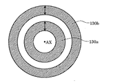
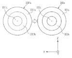
図6は、輪帯照明において形成される二次光源に対する円錐アキシコン系87の作用を説明するための図である。円錐アキシコン系87の間隔が0でかつ後述するズームレンズ90の焦点距離が最小値に設定された状態(以下、「標準状態」という)で形成された最も小さい輪帯状の二次光源130aは、円錐アキシコン系87の間隔を0から所定の値まで拡大させることにより、その幅(外径と内径との差の1/2:図中矢印で示す)が変化することなく、その外径および内径がともに拡大された輪帯状の二次光源130bに変化する。即ち、円錐アキシコン系87の作用により、輪帯状の二次光源の幅が変化することなく、その輪帯比(内径/外径)および大きさ(外径)がともに変化する。
FIG. 6 is a diagram for explaining the action of the
図7は、アフォーカルレンズ85の前側レンズ群85aと後側レンズ群85bとの間の光路中に配置された第1シリンドリカルレンズ対88および第2シリンドリカルレンズ対89の概略構成を示す図である。図7に示すように、第1シリンドリカルレンズ対88は、光源側から順に、たとえばYZ平面内に負屈折力を有し且つXY平面内に無屈折力の第1シリンドリカル負レンズ88aと、同じくYZ平面内に正屈折力を有し且つXY平面内に無屈折力の第1シリンドリカル正レンズ88bとにより構成されている。一方、第2シリンドリカルレンズ対89は、光源側から順に、たとえばXY平面内に負屈折力を有し且つYZ平面内に無屈折力の第2シリンドリカル負レンズ89aと、同じくXY平面内に正屈折力を有し且つYZ平面内に無屈折力の第2シリンドリカル正レンズ89bとにより構成されている。
FIG. 7 is a diagram showing a schematic configuration of the first
第1シリンドリカル負レンズ88aと第1シリンドリカル正レンズ88bとは、光軸AXを中心として一体的に回転するように構成されている。同様に、第2シリンドリカル負レンズ89aと第2シリンドリカル正レンズ89bとは、光軸AXを中心として一体的に回転するように構成されている。第1シリンドリカルレンズ対88はZ方向にパワーを有するビームエキスパンダーとして機能し、第2シリンドリカルレンズ対89はX方向にパワーを有するビームエキスパンダーとして機能する。また、この実施の形態においては、第1シリンドリカルレンズ対88及び第2シリンドリカルレンズ対89のパワーが同一となるように設定されている。従って、第1シリンドリカルレンズ対88及び第2シリンドリカルレンズ対89を通過した光束は、Z方向及びX方向に同一のパワーにより拡大作用を受ける。
The first cylindrical
アフォーカルレンズ85を介した光束は、σ値可変用のズームレンズ90を介して、第2オプティカルインテグレータとしてのマイクロレンズアレイ8に入射する。所定面86の位置はズームレンズ90の前側焦点位置またはその近傍に配置され、マイクロレンズアレイ8の入射面はズームレンズ90の後側焦点面またはその近傍に配置されている。即ち、ズームレンズ90は、所定面86とマイクロレンズアレイ8の入射面とを実質的にフーリエ変換の関係に配置し、ひいてはアフォーカルレンズ85の瞳面とマイクロレンズアレイ8の入射面とを光学的に略共役に配置している。したがって、マイクロレンズアレイ8の入射面上には、アフォーカルレンズ85の瞳面と同様に、例えば光軸AXを中心とした輪帯状の照野が形成される。この輪帯状の照野の全体形状は、ズームレンズ90の焦点距離に依存して相似的に変化する。
The light beam that has passed through the
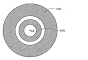
図8は、輪帯照明において形成される二次光源に対するズームレンズ90の作用を説明するための図である。標準状態で形成された輪帯状の二次光源130aは、ズームレンズ90の焦点距離を最小値から所定の値へ拡大させることにより、その全体形状が相似的に拡大された輪帯状の二次光源130cに変化する。即ち、ズームレンズ90の作用により、輪帯状の二次光源の輪帯比が変化することなく、その幅及び大きさ(外径)が共に変化する。
FIG. 8 is a diagram for explaining the action of the
ズームレンズ90を介した光束は、マイクロレンズアレイ8に入射する。ここでズームレンズ90が所定面86での角度変化をマイクロレンズアレイ8の入射面での位置変化(光軸からの距離変化)に変換する機能を有しているため、入射位置変更素子としての円錐アキシコン系87の間隔の変化に伴って、マイクロレンズアレイ8への入射光束の入射位置(光軸からの距離)が変化する。
The light beam that has passed through the
マイクロレンズアレイ8は、縦横にかつ稠密に配列された多数の正屈折力を有する微小レンズからなる光学素子である。マイクロレンズアレイ8を構成する各微小レンズは、マスクMにおいて形成すべき照野の形状(ひいてはウエハW上において形成すべき露光領域の形状)と相似な矩形上の断面を有する。マイクロレンズアレイ8に入射した光束は、多数の微小レンズにより二次元的に分割され、その後側焦点面(ひいては照明瞳)にはマイクロレンズアレイ8への入射光束によって形成される照野と略同じ光強度分布を有する二次光源、即ち光軸AXを中心とした輪帯状の実質的な面光源からなる二次光源が形成される。マイクロレンズアレイ8の後側焦点面に形成された輪帯状の二次光源からの光束は、コンデンサーレンズ9aを介して、マスクブラインドMBを重畳的に照明する。
The
照明視野絞りとしてのマスクブラインドMBには、マイクロレンズアレイ8を構成する各微小レンズの形状と焦点距離とに応じた矩形状の照野が形成される。マスクブラインドMBの矩形状の開口部(光透過部)を介した光束は、結像光学系9bの集光作用を受けた後、所定のパターンが形成されたマスク(被照射面)Mを重畳的に照明する。即ち、結像光学系9bは、マスクブラインドMBの矩形状開口部の像をマスクM上に形成する。マスクMのパターンを透過した光束は、投影光学系PLを介して、感光性基板であるウエハW上にマスクMのパターン像を形成する。こうして、投影光学系PLの光軸AXと直交する平面内においてウエハWを二次元的に駆動制御しながら一括露光またはスキャン露光を行うことにより、ウエハWの各露光領域にはマスクMのパターンが逐次露光される。
In the mask blind MB as an illumination field stop, a rectangular illumination field corresponding to the shape and focal length of each microlens constituting the
この第1の実施の形態にかかる露光装置によれば、この実施の形態にかかる入射位置変更素子としての円錐アキシコン系87がレーザ光源1から射出される照明光のエネルギー密度が高くなる所で用いられた場合においても光学性能を維持することができる結晶材料により形成される結晶光学部材として蛍石により構成されているため、照明光のエネルギー密度が高くなる所に配置される円錐アキシコン系87の内部構造の損傷を防止することができ、円錐アキシコン系87の光透過率の劣化を抑制することができる。従って、円錐アキシコン系87の光学性能を維持した状態で照明光が円錐アキシコン系87を通過するため、照明光の光量の減少を抑えることができ、マスクMを良好に照明することができる。
According to the exposure apparatus of the first embodiment, the
また、円錐アキシコン系87が円錐アキシコン系87を形成する蛍石の結晶方位(111)と光軸AXとが一致するように位置決めされているため、直線偏光状態の照明光が円錐アキシコン系87に入射した場合において、直線偏光の振動方向の変化、直線偏光から楕円偏光や円偏光への変化を防止することができる。従って、マスクMのパターン像の特性に対応した最適な偏光状態の照明光で照明を行うことができる。
Further, since the
次に、図面を参照して、この発明の第2の実施の形態について説明する。この第2の実施の形態にかかる露光装置の構成は、第1の実施の形態にかかる露光装置の円錐アキシコン系87を図9に示す入射位置変更素子としてのフレネルアキシコン系100に変更したものである。従って、第2の実施の形態の説明においては、第1の実施の形態にかかる露光装置の構成と同一の構成の詳細な説明は省略し、第1の実施の形態にかかる露光装置と同一の構成については同一の符号を用いて説明を行う。
Next, a second embodiment of the present invention will be described with reference to the drawings. The configuration of the exposure apparatus according to the second embodiment is such that the
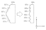
この第2の実施の形態にかかるフレネルアキシコン系100は、照明光学装置の瞳または該瞳の近傍に配置されている。図9は、フレネルアキシコン系100の概略構成を説明するための断面図である。フレネルアキシコン系100は、図9に示すように、光源側から順に、光軸AX方向に対して複数(この実施の形態においては3つ)の凹円錐状の屈折面(凹状屈折面)の一部を有する第1プリズム100a及び第1プリズム100aの凹円錐状の屈折面の一部と互いに当接可能なように相補的に形成された複数(この実施の形態においては3つ)の凸円錐状の屈折面(凸状屈折面)の一部を有する第2プリズム100bを備えている。第1プリズム100aは光源側に平面を向け且つマスクM側に3つの凹円錐状の屈折面の一部を向けて配置されており、第2プリズム100bは光軸側に3つの凸円錐状の屈折面の一部を向け且つマスクM側に平面を向けて配置されている。
The
第1プリズム100aは、3つの凹円錐状の屈折面の一部101a,101b,101cを有している。第1プリズム100aの凹円錐状の屈折面の一部101a,101b,101cは、図10の断面図及び図11の正面図に示す凹円錐状の屈折面を有するプリズム100´aの凹円錐状の屈折面を図10及び図11において破線で示すように区分し平面的に配置したものである。即ち、プリズム100´aの屈折面の領域101´a,101´b,101´cと同一の屈折面を有する。従って、第1プリズム100aに入射し第1プリズム100aの凹円錐状の屈折面の一部101a,101b,101cを通過する光束は、プリズム100´aに入射しプリズム100´aの屈折面の領域101´a,101´b,101´cを通過する光束と同様に屈折する。即ち、第1プリズム100aは、プリズム100´aと同一の機能を有する。
The
第2プリズム100bは、3つの凸円錐状の屈折面の一部102a,102b,102cを有している。第2プリズム100bの凸円錐状の屈折面の一部102a,102b,102cは、図12の断面図及び図13の正面図に示す凸円錐状の屈折面を有するプリズム100´bの凸円錐状の屈折面を図12及び図13において破線で示すように区分し平面的に配置したものである。即ち、プリズム100´bの屈折面の領域102´a,102´b,102´cと同一の屈折面を有する。従って、第2プリズム100bに入射し第2プリズム100bの凸円錐状の屈折面の一部102a,102b,102cを通過する光束は、プリズム100´bに入射しプリズム100´bの屈折面の領域102´a,102´b,102´cを通過する光束と同様に屈折する。即ち、第2プリズム100bは、プリズム100´bと同一の機能を有する。
The
第1プリズム100a及び第2プリズム100bは、結晶材料により形成される結晶光学部材として蛍石により形成されている。図4に示す第1の実施の形態にかかる円錐アキシコン系87と同様に、フレネルアキシコン系100は、フレネルアキシコン系100を形成する蛍石の結晶方位(111)と光軸AXとが一致するように位置決めされており、結晶方位(100)、結晶方位(010)及び結晶方位(001)が所定位置に位置決めされている。
The
また、第1プリズム100a及び第2プリズム100bのうち少なくとも一方は光軸AXに沿って移動可能に構成されており、第1プリズム100aの3つの凹円錐状の屈折面の一部101a〜101cと第2プリズム100bの3つの凸円錐状の屈折面の一部102a〜102cとの間隔が可変に構成されている。ここで、第1プリズム100aの3つの凹円錐状の屈折面の一部101a〜101cと第2プリズム100bの3つの凸円錐状の屈折面の一部102a〜102cとが互いに当接している状態では、フレネルアキシコン系100は平行平面板として機能し、形成される輪帯状の二次光源に及ぼす影響はない。
Further, at least one of the
しかしながら、第1プリズム100aの3つの凹円錐状の屈折面の一部101a〜101cと第2プリズム100bの3つの凸円錐状の屈折面の一部102a〜102cとを離間させると、フレネルアキシコン系100は、いわゆるビームエキスパンダーとして機能する。従って、フレネルアキシコン系100の間隔の変化に伴って、図1中破線で示す所定面86への入射角度が変化し、ズームレンズ90が所定面86での角度変化をマイクロレンズアレイ8の入射面での位置変化(光軸からの距離変化)に変換する機能を有しているため、第2オプティカルインテグレータとしてのマイクロレンズアレイ8への入射光束の入射位置(光軸からの距離)が変化する。従って、図6に示す第1の実施の形態にかかる円錐アキシコン系87の作用と同様に、フレネルアキシコン系100の作用により、輪帯状の二次光源の幅が変化することなく、その輪帯比(内径/外径)および大きさ(外径)がともに変化する。
However, if the
この第2の実施の形態にかかる露光装置によれば、この実施の形態にかかる入射位置変更素子としてのフレネルアキシコン系100がレーザ光源1から射出される照明光のエネルギー密度が高くなる所で用いられた場合においても光学性能を維持することができる蛍石により構成されているため、照明光のエネルギー密度が高くなる所に配置されるフレネルアキシコン系100の内部構造の損傷を防止することができ、フレネルアキシコン系100の光透過率の劣化を抑制することができる。従って、フレネルアキシコン系100の光学性能を維持した状態で照明光がフレネルアキシコン系100を通過するため、照明光の光量の減少を抑えることができ、マスクMを良好に照明することができる。
According to the exposure apparatus according to the second embodiment, the energy density of illumination light emitted from the
また、フレネルアキシコン系100がフレネルアキシコン系100を形成する蛍石の結晶方位(111)と光軸AXとが一致するように位置決めされているため、直線偏光状態の照明光がフレネルアキシコン系100に入射した場合において、直線偏光の振動方向の変化、直線偏光から楕円偏光や円偏光への変化を防止することができる。従って、マスクMのパターン像の特性に対応した最適な偏光状態の照明光で照明を行うことができる。
Further, since the
また、フレネルアキシコン系100が備える第1プリズム100aが平面的に配置される3つの凹円錐状の屈折面の一部101a〜101cを有するため、凹円錐状の屈折面を有するプリズム100´aと比較して第1プリズム100aの厚さを薄くすることができる。また、同様に、フレネルアキシコン系100が備える第2プリズム100bが平面的に配置される3つの凸円錐状の屈折面の一部102a〜102cを有するため、凸円錐状の屈折面を有するプリズム100´bと比較して第2プリズム100bの厚さを薄くすることができる。従って、厚さの薄い第1プリズム100a及び第2プリズム100bを備えるフレネルアキシコン系100の配置スペースを小さくすることができる。
In addition, since the
なお、この第2の実施の形態にかかる第1プリズム100aは3つの凹円錐状の屈折面の一部101a〜101cを有し、第2プリズム100bは3つの凸円錐状の屈折面の一部102a〜102cを有しているが、第1プリズムが2つまたは4つ以上の凹円錐状の屈折面の一部を有し、第2プリズムが2つまたは4つ以上の凸円錐状の屈折面の一部を有するようにしても良い。
The
また、上述の第1及び第2の実施の形態においては、角度変更素子として結晶材料により形成される結晶光学部材として蛍石により形成される光学部材を用いているが、結晶材料により形成される結晶光学部材として蛍石を有する光学部材、結晶材料により形成される結晶光学部材として水晶により形成される光学部材、または、結晶材料により形成される結晶光学部材として水晶を有する光学部材を用いても良い。 In the first and second embodiments described above, the optical member formed of fluorite is used as the crystal optical member formed of the crystal material as the angle changing element, but is formed of the crystal material. An optical member having fluorite as a crystal optical member, an optical member formed of crystal as a crystal optical member formed of a crystal material, or an optical member having crystal as a crystal optical member formed of a crystal material good.
また、上述の第1及び第2の実施の形態においては、入射する直線偏光の光の偏光面を必要に応じて変化させるための位相部材としての1/2波長板10を光源側に配置し、入射する直線偏光の光を必要に応じて非偏光化するためのデポラライザー20をマスク側に配置している。しかしながら、これに限定されることなく、デポラライザー20を光源側に配置し且つ1/2波長板10をマスク側に配置しても同じ光学的な作用効果を得ることができる。
In the first and second embodiments described above, the half-
また、上述の第1及び第2の実施の形態においては、水晶プリズム20aを介した光の進行方向を補償するためのコンペンセーターとして石英プリズム20bを用いている。しかしながら、これに限定されることなく、KrFエキシマレーザー光やArFエキシマレーザー光に対して耐久性の高い光学材料、たとえば水晶や蛍石などにより形成された楔形状のプリズムをコンペンセーターとして用いていることもできる。
In the first and second embodiments described above, the
また、上述の第1及び第2の実施の形態においては、第1オプティカルインテグレータとして回折光学素子を用いているが、第1オプティカルインテグレータとしてフライアイレンズを用いても良い。この場合には、円錐アキシコン系またはフレネルアキシコン系が配置されている位置またはその近傍に位置する照明光学装置の瞳位置において、フライアイレンズがフライアイレンズの入射側に備える多数のレンズ面の輪郭形状(例えば、六角形状や矩形状)に相似した形状の光強度分布が形成される。 In the first and second embodiments described above, a diffractive optical element is used as the first optical integrator, but a fly-eye lens may be used as the first optical integrator. In this case, at the pupil position of the illumination optical device located at or near the position where the conical axicon system or the Fresnel axicon system is arranged, the fly-eye lens has a large number of lens surfaces provided on the incident side of the fly-eye lens. A light intensity distribution having a shape similar to a contour shape (for example, a hexagonal shape or a rectangular shape) is formed.
なお、上述の各実施の形態に係る露光装置において、回折光学素子(DOE)4aからの0次光を遮光するための遮光部材を照明光学系の瞳位置近傍、例えば、第2オプティカルインテグレータとしてのマイクロレンズアレイ8の入射面側又は射出面側に配置しても良い。このような0次光遮光部材は、例えば、特開平4‐225359号や特開2001‐176766号、特開2001‐284240号などに開示されている。このとき特開2001‐284240号に開示される0次光遮光部材では、0次光遮光部材を保持するための4本の弦を互いに直交するように設けているが投影光学系PLに対してマスクMとウエハWとを相対的に移動させつつ露光を行う走査型投影露光装置に適用する場合において、この弦が被照射面上での照明むらに悪影響を及ぼす恐れがある。このときには、0次光遮光部材を保持するための4本の弦のうち、走査方向に対応した方向に沿った2本の弦を取り去り、非走査方向に対応した方向の弦のみで0次光遮光部材を保持することが好ましい。また、弦を非走査方向に対応した方向に延びた3本としても良い(このとき各弦のなす角は120度となる)。また、例えば、特開2001‐176766号に開示されるように光透過性の基板上に遮光部材をパターニングして弦を設けない手法を採用しても良い。
In the exposure apparatus according to each of the above-described embodiments, the light shielding member for shielding the 0th-order light from the diffractive optical element (DOE) 4a is used in the vicinity of the pupil position of the illumination optical system, for example, as a second optical integrator. The
上述の第1及び第2の実施の形態にかかる露光装置では、照明光学装置によってマスク(レチクル)Mを照明し(照明工程)、投影光学系PLを用いてマスクMに形成された転写用のパターンを感光性基板(ウエハ)Wに転写する(転写工程)ことにより、マイクロデバイス(半導体素子、撮像素子、液晶表示素子、薄膜磁気ヘッド等)を製造することができる。以下、第1または第2の実施の形態にかかる露光装置を用いて感光性基板としてのウエハW等に所定の回路パターンを形成することによって、マイクロデバイスとしての半導体デバイスを得る際の手法の一例につき図14のフローチャートを参照して説明する。 In the exposure apparatuses according to the first and second embodiments described above, the mask (reticle) M is illuminated by the illumination optical apparatus (illumination process), and the transfer is formed on the mask M using the projection optical system PL. By transferring the pattern onto the photosensitive substrate (wafer) W (transfer process), a microdevice (semiconductor element, imaging element, liquid crystal display element, thin film magnetic head, etc.) can be manufactured. Hereinafter, an example of a technique for obtaining a semiconductor device as a microdevice by forming a predetermined circuit pattern on a wafer W as a photosensitive substrate using the exposure apparatus according to the first or second embodiment. This will be described with reference to the flowchart of FIG.
先ず、図14のステップS301において、1ロットのウエハW上に金属膜が蒸着される。次のステップS302において、そのlロットのウエハW上の金属膜上にフォトレジストが塗布される。その後、ステップS303において、第1または第2の実施の形態にかかる露光装置を用いて、マスクM上のパターンの像がその投影光学系PLを介して、その1ロットのウエハW上の各ショット領域に順次露光転写される。その後、ステップS304において、その1ロットのウエハW上のフォトレジストの現像が行われた後、ステップS305において、その1ロットのウエハW上でレジストパターンをマスクMとしてエッチングを行うことによって、マスクM上のパターンに対応する回路パターンが、各ウエハW上の各ショット領域に形成される。 First, in step S301 in FIG. 14, a metal film is deposited on one lot of wafers W. In the next step S302, a photoresist is applied on the metal film on the wafer W of the l lot. Thereafter, in step S303, using the exposure apparatus according to the first or second embodiment, an image of the pattern on the mask M is shot on each wafer W of the lot through the projection optical system PL. The area is sequentially exposed and transferred. After that, in step S304, the photoresist on the one lot of wafers W is developed, and in step S305, etching is performed on the one lot of wafers W using the resist pattern as a mask M. A circuit pattern corresponding to the upper pattern is formed in each shot area on each wafer W.
その後、更に上のレイヤの回路パターンの形成等を行うことによって、半導体素子等のデバイスが製造される。上述の半導体デバイス製造方法によれば、第1または第2の実施の形態にかかる照明光学装置を用いているため、照明光の光量の減少を抑えることができ、回路パターンの特性に対応した最適な偏光状態の照明光(露光光)で照明することができる。従って、極めて微細な回路パターンを有する半導体デバイスを精度良く得ることができる。なお、ステップS301〜ステップS305では、ウエハW上に金属を蒸着し、その金属膜上にレジストを塗布、そして露光、現像、エッチングの各工程を行っているが、これらの工程に先立って、ウエハW上にシリコンの酸化膜を形成後、そのシリコンの酸化膜上にレジストを塗布、そして露光、現像、エッチング等の各工程を行っても良いことはいうまでもない。 Thereafter, a device pattern such as a semiconductor element is manufactured by forming a circuit pattern of an upper layer. According to the semiconductor device manufacturing method described above, since the illumination optical device according to the first or second embodiment is used, a decrease in the amount of illumination light can be suppressed, and the optimum corresponding to the characteristics of the circuit pattern It is possible to illuminate with illumination light (exposure light) in a polarized state. Therefore, a semiconductor device having an extremely fine circuit pattern can be obtained with high accuracy. In steps S301 to S305, a metal is deposited on the wafer W, a resist is applied onto the metal film, and exposure, development, and etching processes are performed. Prior to these processes, the wafer is processed. It goes without saying that after a silicon oxide film is formed on W, a resist is applied onto the silicon oxide film, and each step such as exposure, development, and etching may be performed.
また、第1及び第2の実施の形態にかかる露光装置では、プレート(ガラス基板)上に所定のパターン(回路パターン、電極パターン等)を形成することによって、マイクロデバイスとしての液晶表示素子を得ることもできる。以下、図15のフローチャートを参照して、このときの手法の一例につき説明する。図15において、パターン形成工程S401では、第1または第2の実施の形態にかかる露光装置を用いてマスクMのパターンを感光性基板(レジストが塗布されたガラス基板等)に転写露光する、所謂光リソグラフィ工程が実行される。この光リソグラフィー工程によって、感光性基板上には多数の電極等を含む所定パターンが形成される。その後、露光された基板は、現像工程、エッチング工程、レジスト剥離工程等の各工程を経ることによって、基板上に所定のパターンが形成され、次のカラーフィルター形成工程S402へ移行する。 In the exposure apparatus according to the first and second embodiments, a liquid crystal display element as a micro device is obtained by forming a predetermined pattern (circuit pattern, electrode pattern, etc.) on a plate (glass substrate). You can also Hereinafter, an example of the technique at this time will be described with reference to the flowchart of FIG. In FIG. 15, in the pattern formation step S401, the pattern of the mask M is transferred and exposed to a photosensitive substrate (such as a glass substrate coated with a resist) using the exposure apparatus according to the first or second embodiment. An optical lithography process is performed. By this photolithography process, a predetermined pattern including a large number of electrodes and the like is formed on the photosensitive substrate. Thereafter, the exposed substrate is subjected to various processes such as a developing process, an etching process, and a resist stripping process, whereby a predetermined pattern is formed on the substrate, and the process proceeds to the next color filter forming process S402.
次に、カラーフィルター形成工程S402では、R(Red)、G(Green)、B(Blue)に対応した3つのドットの組がマトリックス状に多数配列されたり、またはR、G、Bの3本のストライプのフィルターの組を複数水平走査線方向に配列されたりしたカラーフィルターを形成する。そして、カラーフィルター形成工程S402の後に、セル組み立て工程S403が実行される。セル組み立て工程S403では、パターン形成工程S401にて得られた所定パターンを有する基板、およびカラーフィルター形成工程S402にて得られたカラーフィルター等を用いて液晶パネル(液晶セル)を組み立てる。セル組み立て工程S403では、例えば、パターン形成工程S401にて得られた所定パターンを有する基板とカラーフィルター形成工程S402にて得られたカラーフィルターとの間に液晶を注入して、液晶パネル(液晶セル)を製造する。 Next, in the color filter forming step S402, a large number of groups of three dots corresponding to R (Red), G (Green), and B (Blue) are arranged in a matrix, or three of R, G, and B are arranged. A color filter is formed by arranging a plurality of stripe filter sets in the horizontal scanning line direction. Then, after the color filter formation step S402, a cell assembly step S403 is executed. In the cell assembly step S403, a liquid crystal panel (liquid crystal cell) is assembled using the substrate having the predetermined pattern obtained in the pattern formation step S401, the color filter obtained in the color filter formation step S402, and the like. In the cell assembling step S403, for example, liquid crystal is injected between the substrate having the predetermined pattern obtained in the pattern forming step S401 and the color filter obtained in the color filter forming step S402. ).
その後、モジュール組み立て工程S404にて、組み立てられた液晶パネル(液晶セル)の表示動作を行わせる電気回路、バックライト等の各部品を取り付けて液晶表示素子として完成させる。上述の液晶表示素子の製造方法によれば、第1または第2の実施の形態にかかる照明光学装置を用いているため、照明光の光量の減少を抑えることができ、回路パターンの特性に対応した最適な偏光状態の照明光(露光光)で照明することができる。従って、極めて微細な回路パターンを有する半導体デバイスを精度良く得ることができる。 Thereafter, in a module assembly step S404, components such as an electric circuit and a backlight for performing a display operation of the assembled liquid crystal panel (liquid crystal cell) are attached to complete a liquid crystal display element. According to the above-described method for manufacturing a liquid crystal display element, since the illumination optical device according to the first or second embodiment is used, a decrease in the amount of illumination light can be suppressed, and the characteristics of the circuit pattern can be accommodated. The illumination light (exposure light) having the optimum polarization state can be illuminated. Therefore, a semiconductor device having an extremely fine circuit pattern can be obtained with high accuracy.
1…レーザ光源、2…ビームエキスパンダー、3…折り曲げミラー、4a…回折光学素子、8…マイクロレンズアレイ、9a…コンデンサーレンズ、9b…結像光学系、10…1/2波長板、11…1/4波長板、20…デポラライザー、85…アフォーカルレンズ、87…円錐アキシコン系、87a…第1プリズム、87b…第2プリズム、88…第1シリンドリカルレンズ対、89…第2シリンドリカルレンズ対、90…ズームレンズ、100…フレネルアキシコン系、100a…第1プリズム、100b…第2プリズム、MB…マスクブラインド、M…マスク、PL…投影光学系、W…ウエハ。
DESCRIPTION OF
Claims (10)
前記光源部と前記被照射面との間の光路中に配置される第1オプティカルインテグレータと、
前記第1オプティカルインテグレータと前記被照射面との間の光路中に配置される第2オプティカルインテグレータと、
前記第1オプティカルインテグレータと前記第2オプティカルインテグレータとの間の光路中に配置され、前記第2オプティカルインテグレータへの入射光束の入射位置を変化させる入射位置変更素子と、
を備え、
前記入射位置変更素子は、前記光源部から射出される光束のエネルギー密度が高くなる所で用いられた場合においても前記入射位置変更素子の光学性能を維持することができる光学部材により構成されることを特徴とする照明光学装置。 In the illumination optical device that illuminates the irradiated surface with the light beam from the light source unit,
A first optical integrator disposed in an optical path between the light source unit and the irradiated surface;
A second optical integrator disposed in an optical path between the first optical integrator and the irradiated surface;
An incident position changing element that is arranged in an optical path between the first optical integrator and the second optical integrator and changes an incident position of an incident light beam to the second optical integrator;
With
The incident position changing element is composed of an optical member capable of maintaining the optical performance of the incident position changing element even when used in a place where the energy density of the light beam emitted from the light source unit is high. An illumination optical device.
前記照明光学装置の光軸方向に対して凹状屈折面を有する第1プリズムと、
前記第1プリズムの前記凹状屈折面と相補的に形成された凸状屈折面を有する第2プリズムと、
を備え、
前記第1プリズム及び前記第2プリズムのうち少なくとも一方は、前記照明光学装置の光軸に沿って移動可能に構成されていることを特徴とする請求項1記載の照明光学装置。 The incident position changing element is
A first prism having a concave refractive surface with respect to the optical axis direction of the illumination optical device;
A second prism having a convex refracting surface formed complementary to the concave refracting surface of the first prism;
With
2. The illumination optical apparatus according to claim 1, wherein at least one of the first prism and the second prism is configured to be movable along an optical axis of the illumination optical apparatus.
前記照明光学装置の光軸方向に対して凹状屈折面の一部を有する第1プリズムと、
前記照明光学装置の光軸方向に対して凸状屈折面の一部を有する第2プリズムと、
を備え、
前記第1プリズム及び前記第2プリズムのうちの少なくとも一方は、前記照明光学装置の光軸方向に沿って移動可能に構成され、
前記第1プリズムは複数の前記凹状屈折面の一部を有し、
前記第2プリズムは複数の前記凸状屈折面の一部を有することを特徴とする請求項1記載の照明光学装置。 The incident position changing element is
A first prism having a part of a concave refractive surface with respect to the optical axis direction of the illumination optical device;
A second prism having a part of a convex refractive surface with respect to the optical axis direction of the illumination optical device;
With
At least one of the first prism and the second prism is configured to be movable along the optical axis direction of the illumination optical device,
The first prism has a part of the plurality of concave refractive surfaces,
The illumination optical device according to claim 1, wherein the second prism has a part of the plurality of convex refractive surfaces.
前記マスクを照明するための請求項1乃至請求項8の何れか一項に記載の照明光学装置と、
前記マスクのパターンの像を前記感光性基板上に形成するための投影光学系と、
を備えることを特徴とする露光装置。 In an exposure apparatus that transfers a mask pattern onto a photosensitive substrate,
The illumination optical apparatus according to any one of claims 1 to 8, for illuminating the mask;
A projection optical system for forming an image of the mask pattern on the photosensitive substrate;
An exposure apparatus comprising:
請求項1乃至請求項8の何れか一項に記載の照明光学装置を用いて前記所定のパターンが形成されるマスクを照明する照明工程と、
前記感光性基板上に前記所定のパターンを転写する転写工程と、
を含むことを特徴とする露光方法。 In an exposure method for transferring a predetermined pattern onto a photosensitive substrate,
An illumination process for illuminating a mask on which the predetermined pattern is formed using the illumination optical apparatus according to any one of claims 1 to 8.
A transfer step of transferring the predetermined pattern onto the photosensitive substrate;
An exposure method comprising:
Priority Applications (1)
| Application Number | Priority Date | Filing Date | Title |
|---|---|---|---|
| JP2004051442A JP2005243904A (en) | 2004-02-26 | 2004-02-26 | Illumination optical apparatus, aligner, and exposure method |
Applications Claiming Priority (1)
| Application Number | Priority Date | Filing Date | Title |
|---|---|---|---|
| JP2004051442A JP2005243904A (en) | 2004-02-26 | 2004-02-26 | Illumination optical apparatus, aligner, and exposure method |
Publications (2)
| Publication Number | Publication Date |
|---|---|
| JP2005243904A true JP2005243904A (en) | 2005-09-08 |
| JP2005243904A5 JP2005243904A5 (en) | 2008-03-21 |
Family
ID=35025321
Family Applications (1)
| Application Number | Title | Priority Date | Filing Date |
|---|---|---|---|
| JP2004051442A Pending JP2005243904A (en) | 2004-02-26 | 2004-02-26 | Illumination optical apparatus, aligner, and exposure method |
Country Status (1)
| Country | Link |
|---|---|
| JP (1) | JP2005243904A (en) |
Cited By (11)
| Publication number | Priority date | Publication date | Assignee | Title |
|---|---|---|---|---|
| WO2006043458A1 (en) * | 2004-10-19 | 2006-04-27 | Nikon Corporation | Lighting optical device, exposure system, and exposure method |
| CN102221785A (en) * | 2010-04-14 | 2011-10-19 | 上海微电子装备有限公司 | Photolithographic illumination device using mercury lamp light source |
| WO2011152523A1 (en) * | 2010-06-03 | 2011-12-08 | 株式会社ニコン | Microscope device |
| US20130271945A1 (en) | 2004-02-06 | 2013-10-17 | Nikon Corporation | Polarization-modulating element, illumination optical apparatus, exposure apparatus, and exposure method |
| US9341954B2 (en) | 2007-10-24 | 2016-05-17 | Nikon Corporation | Optical unit, illumination optical apparatus, exposure apparatus, and device manufacturing method |
| US9423698B2 (en) | 2003-10-28 | 2016-08-23 | Nikon Corporation | Illumination optical apparatus and projection exposure apparatus |
| US9678437B2 (en) | 2003-04-09 | 2017-06-13 | Nikon Corporation | Illumination optical apparatus having distribution changing member to change light amount and polarization member to set polarization in circumference direction |
| US9678332B2 (en) | 2007-11-06 | 2017-06-13 | Nikon Corporation | Illumination apparatus, illumination method, exposure apparatus, and device manufacturing method |
| US9885872B2 (en) | 2003-11-20 | 2018-02-06 | Nikon Corporation | Illumination optical apparatus, exposure apparatus, and exposure method with optical integrator and polarization member that changes polarization state of light |
| US9891539B2 (en) | 2005-05-12 | 2018-02-13 | Nikon Corporation | Projection optical system, exposure apparatus, and exposure method |
| US10101666B2 (en) | 2007-10-12 | 2018-10-16 | Nikon Corporation | Illumination optical apparatus, exposure apparatus, and device manufacturing method |
-
2004
- 2004-02-26 JP JP2004051442A patent/JP2005243904A/en active Pending
Cited By (24)
| Publication number | Priority date | Publication date | Assignee | Title |
|---|---|---|---|---|
| US9885959B2 (en) | 2003-04-09 | 2018-02-06 | Nikon Corporation | Illumination optical apparatus having deflecting member, lens, polarization member to set polarization in circumference direction, and optical integrator |
| US9678437B2 (en) | 2003-04-09 | 2017-06-13 | Nikon Corporation | Illumination optical apparatus having distribution changing member to change light amount and polarization member to set polarization in circumference direction |
| US9423698B2 (en) | 2003-10-28 | 2016-08-23 | Nikon Corporation | Illumination optical apparatus and projection exposure apparatus |
| US9760014B2 (en) | 2003-10-28 | 2017-09-12 | Nikon Corporation | Illumination optical apparatus and projection exposure apparatus |
| US10281632B2 (en) | 2003-11-20 | 2019-05-07 | Nikon Corporation | Illumination optical apparatus, exposure apparatus, and exposure method with optical member with optical rotatory power to rotate linear polarization direction |
| US9885872B2 (en) | 2003-11-20 | 2018-02-06 | Nikon Corporation | Illumination optical apparatus, exposure apparatus, and exposure method with optical integrator and polarization member that changes polarization state of light |
| US20130271945A1 (en) | 2004-02-06 | 2013-10-17 | Nikon Corporation | Polarization-modulating element, illumination optical apparatus, exposure apparatus, and exposure method |
| US10241417B2 (en) | 2004-02-06 | 2019-03-26 | Nikon Corporation | Polarization-modulating element, illumination optical apparatus, exposure apparatus, and exposure method |
| US10234770B2 (en) | 2004-02-06 | 2019-03-19 | Nikon Corporation | Polarization-modulating element, illumination optical apparatus, exposure apparatus, and exposure method |
| US10007194B2 (en) | 2004-02-06 | 2018-06-26 | Nikon Corporation | Polarization-modulating element, illumination optical apparatus, exposure apparatus, and exposure method |
| US8004658B2 (en) | 2004-10-19 | 2011-08-23 | Nikon Corporation | Lighting optical device, exposure system, and exposure method |
| JP2006120675A (en) * | 2004-10-19 | 2006-05-11 | Nikon Corp | Optical illumination device, aligner, and exposure method |
| WO2006043458A1 (en) * | 2004-10-19 | 2006-04-27 | Nikon Corporation | Lighting optical device, exposure system, and exposure method |
| JP4535260B2 (en) * | 2004-10-19 | 2010-09-01 | 株式会社ニコン | Illumination optical apparatus, exposure apparatus, and exposure method |
| US9891539B2 (en) | 2005-05-12 | 2018-02-13 | Nikon Corporation | Projection optical system, exposure apparatus, and exposure method |
| US10101666B2 (en) | 2007-10-12 | 2018-10-16 | Nikon Corporation | Illumination optical apparatus, exposure apparatus, and device manufacturing method |
| US9857599B2 (en) | 2007-10-24 | 2018-01-02 | Nikon Corporation | Optical unit, illumination optical apparatus, exposure apparatus, and device manufacturing method |
| US9341954B2 (en) | 2007-10-24 | 2016-05-17 | Nikon Corporation | Optical unit, illumination optical apparatus, exposure apparatus, and device manufacturing method |
| US9678332B2 (en) | 2007-11-06 | 2017-06-13 | Nikon Corporation | Illumination apparatus, illumination method, exposure apparatus, and device manufacturing method |
| CN102221785A (en) * | 2010-04-14 | 2011-10-19 | 上海微电子装备有限公司 | Photolithographic illumination device using mercury lamp light source |
| JP5459399B2 (en) * | 2010-06-03 | 2014-04-02 | 株式会社ニコン | Microscope equipment |
| WO2011152523A1 (en) * | 2010-06-03 | 2011-12-08 | 株式会社ニコン | Microscope device |
| EP2579084A4 (en) * | 2010-06-03 | 2017-04-12 | Nikon Corporation | Microscope device |
| US8773758B2 (en) | 2010-06-03 | 2014-07-08 | Nikon Corporation | Microscope apparatus with an imaging system including an astigmatic difference changing device |
Similar Documents
| Publication | Publication Date | Title |
|---|---|---|
| JP6493325B2 (en) | Flux conversion element, illumination optical device, exposure apparatus, and exposure method | |
| JP4849165B2 (en) | Illumination optical apparatus, exposure apparatus, and exposure method | |
| JP4465720B2 (en) | Optical system, exposure apparatus, and exposure method | |
| JPWO2005010963A1 (en) | Illumination optical apparatus, exposure apparatus, and exposure method | |
| JP2005156592A (en) | Illumination optical device, exposure device and exposure method | |
| JP4976094B2 (en) | Illumination optical apparatus, exposure apparatus, exposure method, and microdevice manufacturing method | |
| JP2005243904A (en) | Illumination optical apparatus, aligner, and exposure method | |
| WO2011158912A1 (en) | Illuminating optical system, expose device, and device production method | |
| JP2005108925A (en) | Lighting optical device, exposure apparatus and exposure method | |
| JP2005302826A (en) | Lighting optical device, exposure system and method | |
| JP5531518B2 (en) | Polarization conversion unit, illumination optical system, exposure apparatus, and device manufacturing method | |
| JP2007048871A (en) | Illuminating optical device, exposure device and manufacturing method for micro-device | |
| JP2007027658A (en) | Illumination optical apparatus, exposure apparatus, and manufacturing method of micro device | |
| JP4581743B2 (en) | Illumination optical apparatus, exposure apparatus, and microdevice manufacturing method | |
| JP5534276B2 (en) | Illumination optical system, exposure apparatus, and device manufacturing method | |
| JP2007158271A (en) | Illumination optical device, exposure system, and method for manufacturing device | |
| JP2006100429A (en) | Projection optical system, exposure device, and exposure method |
Legal Events
| Date | Code | Title | Description |
|---|---|---|---|
| A621 | Written request for application examination |
Free format text: JAPANESE INTERMEDIATE CODE: A621 Effective date: 20070104 |
|
| A521 | Written amendment |
Free format text: JAPANESE INTERMEDIATE CODE: A523 Effective date: 20080131 |
|
| A977 | Report on retrieval |
Free format text: JAPANESE INTERMEDIATE CODE: A971007 Effective date: 20081001 |
|
| A131 | Notification of reasons for refusal |
Free format text: JAPANESE INTERMEDIATE CODE: A131 Effective date: 20081118 |
|
| A02 | Decision of refusal |
Free format text: JAPANESE INTERMEDIATE CODE: A02 Effective date: 20090407 |