JP2005195427A - Current measurement system, current measurement method, and current measurement program - Google Patents
Current measurement system, current measurement method, and current measurement program Download PDFInfo
- Publication number
- JP2005195427A JP2005195427A JP2004001214A JP2004001214A JP2005195427A JP 2005195427 A JP2005195427 A JP 2005195427A JP 2004001214 A JP2004001214 A JP 2004001214A JP 2004001214 A JP2004001214 A JP 2004001214A JP 2005195427 A JP2005195427 A JP 2005195427A
- Authority
- JP
- Japan
- Prior art keywords
- magnetic
- current
- conductor
- measured
- magnetic sensors
- Prior art date
- Legal status (The legal status is an assumption and is not a legal conclusion. Google has not performed a legal analysis and makes no representation as to the accuracy of the status listed.)
- Pending
Links
Images


Abstract
Description
本発明は、磁気センサを用いて被測定導体に流れる電流の大きさを測定する電流測定装置および電流測定方法に関し、特に、複数の磁気センサを被測定導体に近接して配置する電流測定装置、電流測定方法および電流測定プログラムに関する。 The present invention relates to a current measuring device and a current measuring method for measuring the magnitude of a current flowing through a conductor to be measured using a magnetic sensor, and in particular, a current measuring device in which a plurality of magnetic sensors are arranged close to a conductor to be measured, The present invention relates to a current measurement method and a current measurement program.
導体に流れる電流の大きさを測定する従来の技術として、磁気センサを用いた電流の測定方法が知られている。磁気センサでは、センサ内部に磁気検出素子が設けられ、その磁気検出素子に入力される磁界の大きさに比例した電圧を出力する。
そして、この磁気センサを用いて電流を測定する場合、磁気センサを導体の周辺に配置し、導体に流れる電流による誘導磁界を磁気センサで検出することにより、導体に流れる電流の大きさを測定することができる。
As a conventional technique for measuring the magnitude of a current flowing through a conductor, a current measuring method using a magnetic sensor is known. In a magnetic sensor, a magnetic detection element is provided inside the sensor, and a voltage proportional to the magnitude of a magnetic field input to the magnetic detection element is output.
When measuring the current using this magnetic sensor, the magnitude of the current flowing through the conductor is measured by arranging the magnetic sensor around the conductor and detecting the induced magnetic field caused by the current flowing through the conductor with the magnetic sensor. be able to.
また、被測定導体を有する基板上に表面実装の可能な磁気センサを配置して、電流の大きさを測定する電流測定装置がある。この電流測定装置では、磁気センサが実装面に対して平行な磁界を検出することができる。このため、被測定導体上に磁気センサを配置し、導体の幅方向に生じる磁界を磁気センサで検出することにより、導体に流れる電流の大きさを測定することができる。
また、例えば、特許文献1には、導体に流れる電流を磁気センサで測定する際の外乱磁場の影響を軽減するため、磁気センサを2個使用する方法が開示されている。
Further, for example, Patent Document 1 discloses a method of using two magnetic sensors in order to reduce the influence of a disturbing magnetic field when measuring a current flowing through a conductor with a magnetic sensor.
しかしながら、特許文献1に開示された方法では、磁気センサの配置位置と被測定導体の形状に制約が存在した。
すなわち、特許文献1に開示された方法では、外乱磁場に対する磁気センサの出力を一致させるために、2個の磁気センサが同一円周上に配置されるように被測定導体を挟み込み、2個の磁気センサの電流感度が互いに等しくなるようにする必要がある。もし、これらの磁気センサの配置が同一円周上からずれた場合、外乱磁場の大きさと方向が異なるため、外乱磁場をキャンセルできなくなり、電流の測定精度が劣化するという問題があった。
However, in the method disclosed in Patent Document 1, there are restrictions on the arrangement position of the magnetic sensor and the shape of the conductor to be measured.
That is, in the method disclosed in Patent Document 1, in order to match the output of the magnetic sensor with respect to the disturbance magnetic field, the conductor to be measured is sandwiched so that the two magnetic sensors are arranged on the same circumference. It is necessary to make the current sensitivities of the magnetic sensors equal to each other. If the arrangement of these magnetic sensors deviates from the same circumference, the disturbance magnetic field is different in magnitude and direction, so that the disturbance magnetic field cannot be canceled and the current measurement accuracy deteriorates.
また、磁気センサの配置位置や被測定導体の形状が制限を受けると、電流測定装置の大きさや形状が制約を受けたり、被測定導体に対して等間隔に磁気センサを配置するために、特殊な治具やスペーサ等が必要になったりするという問題があった。
また、磁気センサの電流感度は、ホール素子の磁気感度と被測定導体の距離に大きく影響を受ける。このため、被測定導体に流れる電流を精度よく測定するためには、2個の磁気センサを正確に配置し、被測定導体に流れる電流に対する電流感度を揃える必要があり、被測定導体に流れる電流の測定精度が、磁気センサの電流感度のバラツキに大きく影響を受けるという問題があった。
In addition, if the position of the magnetic sensor and the shape of the conductor to be measured are restricted, the size and shape of the current measuring device are restricted, or the magnetic sensor is placed at regular intervals with respect to the conductor to be measured. There is a problem that a jig or a spacer is required.
Further, the current sensitivity of the magnetic sensor is greatly influenced by the magnetic sensitivity of the Hall element and the distance of the conductor to be measured. For this reason, in order to accurately measure the current flowing through the conductor to be measured, it is necessary to arrange two magnetic sensors accurately and to equalize the current sensitivity to the current flowing through the conductor to be measured. The measurement accuracy is greatly affected by variations in the current sensitivity of the magnetic sensor.
さらに、特許文献1に開示された方法では、被測定導体が円柱状(または線状)の導体(または導線)の場合については、優れた測定精度を実現できるが、円柱以外の形状の被測定導体に流れる電流の測定については考慮されていなかった。
そこで、本発明の目的は、磁気センサの配置位置および被測定導体の形状に対する制約を緩和しつつ、被測定導体に流れる電流の測定精度を向上させることが可能な電流測定装置、電流測定方法および電流測定プログラムを提供することである。
Furthermore, in the method disclosed in Patent Document 1, excellent measurement accuracy can be achieved when the conductor to be measured is a cylindrical (or linear) conductor (or conductor), but the shape of the object to be measured is other than a cylinder. Measurement of the current flowing through the conductor was not considered.
Accordingly, an object of the present invention is to provide a current measuring apparatus, a current measuring method, and a current measuring apparatus capable of improving the measurement accuracy of a current flowing through a measured conductor while relaxing restrictions on the arrangement position of the magnetic sensor and the shape of the measured conductor. It is to provide a current measurement program.
上述した課題を解決するために、請求項1記載の電流測定装置によれば、複数の磁気センサと、前記磁気センサの電流感度の差異が反映された出力信号に基づいて、被測定導体に流れる電流の値を算出する信号処理手段とを備えることを特徴とする。
これにより、被測定導体に流れる電流の値を算出する際に、磁気センサの電流感度を互いに異ならせることが可能となり、外乱磁場の影響を軽減するために、磁気センサの電流感度を互いに一致させる必要がなくなる。このため、磁気センサの配置位置および被測定導体の形状に対する制約を緩和しつつ、被測定導体に流れる電流の測定精度を向上させることが可能となり、磁気センサの低価格化および小型化を図りつつ、被測定導体に流れる電流の測定を手軽に行うことが可能となる。
In order to solve the above-described problem, according to the current measuring device according to claim 1, the current flows to the conductor under measurement based on a plurality of magnetic sensors and an output signal reflecting a difference in current sensitivity between the magnetic sensors. Signal processing means for calculating a current value.
As a result, when calculating the value of the current flowing through the conductor to be measured, the current sensitivities of the magnetic sensors can be made different from each other, and the current sensitivities of the magnetic sensors are made to coincide with each other in order to reduce the influence of the disturbance magnetic field. There is no need. For this reason, it becomes possible to improve the measurement accuracy of the current flowing through the conductor to be measured while relaxing restrictions on the arrangement position of the magnetic sensor and the shape of the conductor to be measured, thereby reducing the price and size of the magnetic sensor. Thus, it is possible to easily measure the current flowing through the conductor to be measured.
また、請求項2記載の電流測定装置によれば、前記磁気センサは、感磁面が互いに平行に配置された磁電変換素子を備えることを特徴とする。
これにより、複数の磁気センサに対する外乱磁場の大きさと方向を容易に一致させることが可能となり、複数の磁気センサからの出力信号の差分をとることで、外乱磁場をキャンセルすることができる。
また、請求項3記載の電流測定装置によれば、前記複数の磁気センサの磁場感度は互いに等しいことを特徴とする。
これにより、複数の磁気センサからの出力信号の差分をとることで、外乱磁場をキャンセルすることができ、被測定導体に流れる電流の測定精度を向上させることが可能となる。
According to a second aspect of the present invention, the magnetic sensor includes a magnetoelectric conversion element having magnetic sensitive surfaces arranged in parallel to each other.
This makes it possible to easily match the magnitude and direction of the disturbance magnetic field with respect to the plurality of magnetic sensors, and cancel the disturbance magnetic field by taking the difference between the output signals from the plurality of magnetic sensors.
According to the current measuring device of the third aspect, the magnetic field sensitivities of the plurality of magnetic sensors are equal to each other.
Thereby, by taking the difference between the output signals from the plurality of magnetic sensors, the disturbance magnetic field can be canceled, and the measurement accuracy of the current flowing through the conductor to be measured can be improved.
また、請求項4記載の電流測定装置によれば、感磁面が互いに平行になるように前記複数の磁気センサが実装された基材をさらに備えることを特徴とする。
これにより、被測定導体に対して磁気センサが非対称となるように基材を被測定導体の近傍に設置するだけで、複数の磁気センサの感磁面を互いに平行にすることが可能となるとともに、磁気センサの電流感度を互いに異ならせることが可能となる。このため、外乱磁場の影響を軽減することを可能としつつ、被測定導体に流れる電流の測定することが可能となり、測定導体に流れる電流の測定精度を向上させることが可能となるとともに、被測定導体の形状に対する制約を緩和しつつ、被測定導体に流れる電流の測定を手軽に行うことが可能となる。
According to a fourth aspect of the present invention, there is provided the current measuring device further comprising a base material on which the plurality of magnetic sensors are mounted such that the magnetic sensitive surfaces are parallel to each other.
As a result, the magnetic sensitive surfaces of the plurality of magnetic sensors can be made parallel to each other only by placing the base material in the vicinity of the measured conductor so that the magnetic sensor is asymmetric with respect to the measured conductor. The current sensitivities of the magnetic sensors can be made different from each other. For this reason, it is possible to measure the current flowing through the conductor to be measured while reducing the influence of the disturbance magnetic field, and to improve the measurement accuracy of the current flowing through the conductor to be measured. It is possible to easily measure the current flowing through the conductor to be measured while relaxing restrictions on the shape of the conductor.
また、請求項5記載の電流測定装置によれば、前記磁気センサは、ホール素子と、前記ホール素子の感磁面に対して平行に配置され、前記被測定導体に流れる電流により発生する磁場を収束させ、前記収束させた磁場の垂直成分を前記ホール素子の感磁面に導く磁気収束板とを備えることを特徴とする。
これにより、被測定導体から発生する磁場に対してホール素子の感磁面を平行に配置した場合においても、被測定導体から発生する磁場を効率よく検出することが可能となり、被測定導体上に磁気センサを水平に配置することを可能としつつ、被測定導体に流れる電流を精度よく測定することが可能となる。
According to the current measuring device of
As a result, even when the magnetic sensing surface of the Hall element is arranged in parallel to the magnetic field generated from the conductor to be measured, the magnetic field generated from the conductor to be measured can be efficiently detected. While making it possible to arrange the magnetic sensor horizontally, the current flowing through the conductor to be measured can be accurately measured.
また、請求項6記載の電流測定装置によれば、前記信号処理手段は、前記複数の磁気センサのうち2個の磁気センサの磁場感度、前記2個の磁気センサの電流感度および前記2個の磁気センサの出力信号の値に基づいて、前記被測定導体に流れる電流の値を算出することを特徴とする。
これにより、磁気センサの電流感度が互いに異なる場合においても、演算処理によって被測定導体に流れる電流の値を算出することができ、磁気センサの配置位置および被測定導体の形状に対する制約を緩和しつつ、被測定導体に流れる電流の値の測定を手軽に行うことが可能となる。
Further, according to the current measuring device of
Thereby, even when the current sensitivities of the magnetic sensors are different from each other, the value of the current flowing through the conductor to be measured can be calculated by the arithmetic processing, and the restrictions on the position of the magnetic sensor and the shape of the conductor to be measured are relaxed. Therefore, it is possible to easily measure the value of the current flowing through the conductor to be measured.
また、請求項7記載の電流測定装置によれば、前記2個の磁気センサの電流感度がそれぞれSa、Sb[V/A]であり、前記2個の磁気センサの出力信号の値がそれぞれVa、Vb[V]である時、前記被測定導体に流れる電流の値I[A]は、I=(Va−Vb)/(Sa−Sb)であることを特徴とする。
これにより、複数の磁気センサからの出力信号の差分をとることで、外乱磁場をキャンセルすることができる。このため、磁気センサの電流感度および磁気センサの出力信号の値を用いることで、被測定導体に流れる電流の値を算出することが可能となり、被測定導体に流れる電流の測定精度を向上させることが可能となる。
According to the current measuring device of claim 7, the current sensitivities of the two magnetic sensors are Sa and Sb [V / A], respectively, and the values of the output signals of the two magnetic sensors are Va. , Vb [V], the current value I [A] flowing through the conductor to be measured is I = (Va−Vb) / (Sa−Sb).
Thereby, the disturbance magnetic field can be canceled by taking the difference between the output signals from the plurality of magnetic sensors. Therefore, by using the current sensitivity of the magnetic sensor and the value of the output signal of the magnetic sensor, the value of the current flowing through the conductor to be measured can be calculated, and the measurement accuracy of the current flowing through the conductor to be measured is improved. Is possible.
また、請求項8記載の電流測定装置によれば、前記信号処理手段は、前記被測定導体に流れる既知の電流値と、その時の前記2個の磁気センサの出力信号の値に基づいて、前記2個の磁気センサの電流感度の差分(Sa−Sb)を予め算出するキャリブレーション手段をさらに備えることを特徴とする。
これにより、磁気センサの電流感度の差分を簡易に求めることが可能となるとともに、磁気センサの個々の電流感度を求めることなく、被測定導体に流れる電流を算出することが可能となり、被測定導体に流れる電流の測定を手軽に行うことが可能となる。
Further, according to the current measuring device according to claim 8, the signal processing means is configured based on a known current value flowing through the conductor to be measured and output signal values of the two magnetic sensors at that time. It further comprises calibration means for preliminarily calculating a difference (Sa−Sb) in current sensitivity between the two magnetic sensors.
This makes it possible to easily obtain the difference in current sensitivity of the magnetic sensor, and to calculate the current flowing through the measured conductor without obtaining the individual current sensitivity of the magnetic sensor. It is possible to easily measure the current flowing through the.
また、請求項9記載の電流測定方法によれば、被測定導体に流れる電流に対する電流感度が互いに異なるように複数の磁気センサを配置するステップと、前記磁気センサからの出力信号を取り込むステップと、前記複数の磁気センサから取り込まれた出力信号に基づいて、前記被測定導体に流れる電流の値を算出するステップとを備えることを特徴とする。
これにより、被測定導体に流れる電流を測定する際に、磁気センサの電流感度が互いに一致するように磁気センサを配置することなく、外乱磁場の影響を軽減することが可能となり、磁気センサの配置位置および被測定導体の形状に対する制約を緩和しつつ、被測定導体に流れる電流の測定精度を向上させることができる。
According to the current measurement method of claim 9, the step of arranging a plurality of magnetic sensors so that the current sensitivities to the current flowing through the conductor to be measured are different from each other, and the step of capturing the output signal from the magnetic sensor; Calculating a value of a current flowing through the conductor to be measured based on output signals taken from the plurality of magnetic sensors.
As a result, when measuring the current flowing through the conductor to be measured, it is possible to reduce the influence of the disturbance magnetic field without arranging the magnetic sensor so that the current sensitivities of the magnetic sensors match each other. The measurement accuracy of the current flowing in the conductor to be measured can be improved while relaxing restrictions on the position and the shape of the conductor to be measured.
また、請求項10記載の電流測定方法によれば、前記複数の磁気センサは感磁面を有する磁電変換素子を有し、前記感磁面は前記被測定導体に流れる電流により発生する磁場に対して垂直であることを特徴とする。
これにより、被測定導体から発生する磁場を効率よく検出することを可能としつつ、複数の磁気センサに対する外乱磁場の大きさと方向を容易に一致させることが可能となる。このため、複数の磁気センサからの出力信号の差分をとることで、外乱磁場をキャンセルすることが可能となるとともに、被測定導体に流れる電流の値を精度よく測定することが可能となる。
According to the current measurement method of claim 10, the plurality of magnetic sensors include magnetoelectric transducers having a magnetic sensitive surface, and the magnetic sensitive surface is adapted to a magnetic field generated by a current flowing through the measured conductor. It is characterized by being vertical.
As a result, it is possible to easily detect the magnetic field generated from the conductor to be measured, and to easily match the magnitude and direction of the disturbance magnetic field with respect to the plurality of magnetic sensors. For this reason, by taking the difference between the output signals from the plurality of magnetic sensors, the disturbance magnetic field can be canceled and the value of the current flowing through the conductor to be measured can be accurately measured.
また、請求項11記載の電流測定方法によれば、前記複数の磁気センサは感磁面を有する磁電変換素子を有し、前記感磁面は前記被測定導体に流れる電流により発生する磁場に対して平行であることを特徴とする。
これにより、複数の磁気センサに対する外乱磁場の大きさと方向を容易に一致させることが可能となり、複数の磁気センサからの出力信号の差分をとることで、外乱磁場をキャンセルすることができる。
また、請求項12記載の電流測定方法によれば、前記被測定導体がブスバーであることを特徴とする。
これにより、被測定導体の形状に対する制約を緩和しつつ、被測定導体に流れる電流を測定することができ、円柱以外の形状の被測定導体に流れる電流の値を精度よく測定することができる。
According to the current measuring method of
This makes it possible to easily match the magnitude and direction of the disturbance magnetic field with respect to the plurality of magnetic sensors, and cancel the disturbance magnetic field by taking the difference between the output signals from the plurality of magnetic sensors.
The current measuring method according to claim 12 is characterized in that the conductor to be measured is a bus bar.
As a result, it is possible to measure the current flowing through the conductor to be measured while relaxing restrictions on the shape of the conductor to be measured, and to accurately measure the value of the current flowing through the conductor to be measured having a shape other than the cylinder.
また、請求項13記載の電流測定プログラムによれば、被測定導体に流れる電流に対する電流感度が互いに異なるように配置された複数の磁気センサからの出力信号を取り込むステップと、前記複数の磁気センサから取り込まれた出力信号に基づいて、前記被測定導体に流れる電流の値を算出するステップとをコンピュータに実行させることを特徴とする。
これにより、磁気センサの電流感度が互いに一致するように磁気センサを配置させることなく、被測定導体に流れる電流を測定する際の外乱磁場の影響を軽減することが可能となり、磁気センサの低価格化および小型化を図りつつ、被測定導体に流れる電流の測定精度を向上させることができる。
According to the current measurement program of the thirteenth aspect of the present invention, the step of acquiring output signals from a plurality of magnetic sensors arranged so that the current sensitivities to the current flowing through the conductor to be measured are different from each other; And causing the computer to execute a step of calculating a value of a current flowing through the conductor to be measured based on the fetched output signal.
As a result, it is possible to reduce the influence of the disturbance magnetic field when measuring the current flowing through the conductor to be measured without arranging the magnetic sensors so that the current sensitivities of the magnetic sensors coincide with each other. The measurement accuracy of the current flowing through the conductor to be measured can be improved while reducing the size and size.
以上説明したように、本発明によれば、被測定導体に流れる電流に対する電流感度が互いに異なるように磁気センサを配置し、これらの磁気センサからの出力信号に基づいて被測定導体に流れる電流の値を算出することにより、磁気センサの電流感度が互いに一致するように磁気センサを配置することなく、外乱磁場の影響を軽減することができる。このため、磁気センサの配置位置および被測定導体の形状に対する制約を緩和しつつ、被測定導体に流れる電流の測定精度を向上させることが可能となり、磁気センサの低価格化および小型化を図りつつ、被測定導体に流れる電流の測定を手軽に行うことが可能となる。 As described above, according to the present invention, the magnetic sensors are arranged so that the current sensitivities to the currents flowing through the conductors to be measured are different from each other, and the currents flowing through the conductors to be measured based on the output signals from these magnetic sensors. By calculating the value, it is possible to reduce the influence of the disturbance magnetic field without arranging the magnetic sensors so that the current sensitivities of the magnetic sensors coincide with each other. For this reason, it becomes possible to improve the measurement accuracy of the current flowing through the conductor to be measured while relaxing restrictions on the arrangement position of the magnetic sensor and the shape of the conductor to be measured, thereby reducing the price and size of the magnetic sensor. Thus, it is possible to easily measure the current flowing through the conductor to be measured.
以下、本発明の実施形態に係る電流測定装置および電流測定方法について図面を参照しながら説明する。
図1は、本発明の第1実施形態に係る電流測定装置の概略構成を示す斜視図である。
図1において、プリント基板1上には、2個のワンパッケージ磁気センサ2a、2bが実装されている。ここで、ワンパッケージ磁気センサ2a、2bの内部には、磁気センサ3a、3bがそれぞれ内蔵されるとともに、磁気センサ3a、3bからの出力信号に基づいて、被測定導体5に流れる電流Iの値を算出する信号処理部4a、4bが内蔵されている。なお、被測定導体5としては、例えば、ブスバー、円柱状導体または導線などを挙げることができる。
Hereinafter, a current measuring device and a current measuring method according to embodiments of the present invention will be described with reference to the drawings.
FIG. 1 is a perspective view showing a schematic configuration of a current measuring apparatus according to the first embodiment of the present invention.
In FIG. 1, two one-package
また、磁気センサ3a、3bとしては、例えば、ホール素子やMR、強磁性MRなどの磁電変換素子を用いることができ、これらの磁電変換素子の感磁面が互いに平行になるように、ワンパッケージ磁気センサ2a、2bをプリント基板1上に配置することができる。
そして、被測定導体5に流れる電流Iの値を測定する場合、被測定導体5に対して磁気センサ3a、3bが非対称に配置されるように、ワンパッケージ磁気センサ2a、2bを被測定導体5の近傍に設置する。
In addition, as the
When measuring the value of the current I flowing through the conductor to be measured 5, the one-package
ここで、磁気センサ3a、3bの感磁面が互いに平行になるように、ワンパッケージ磁気センサ2a、2bをプリント基板1上に配置することにより、ワンパッケージ磁気センサ2a、2bが実装されたプリント基板1を被測定導体5の近傍に設置するだけで、被測定導体5に対する磁気センサ3a、3bの感磁面の方向を互いに揃えることができる。
そして、被測定導体5の手前から奥に向かって電流Iが流れると、被測定導体5の周囲に磁場6が生成される。そして、被測定導体5の周囲に生成された磁場6の一部6a、6bは、磁気センサ3a、3bをそれぞれ貫通し、磁気センサ3a、3bは、被測定導体5の周囲に生成された磁場6の一部6a、6bをそれぞれ感知することができる。
Here, the one-package
When a current I flows from the front of the conductor to be measured 5 toward the back, a
そして、磁気センサ3a、3bは、被測定導体5の周囲に生成された磁場6の一部6a、6bを感知すると、信号処理部4a、4bは、磁気センサ3a、3bからの出力信号に基づいて、被測定導体5に流れる電流Iの値を算出することができる。
ここで、被測定導体5に対して磁気センサ3a、3bを非対称に配置するとともに、磁気センサ3a、3bの感磁面の方向を揃えて配置することにより、磁気センサ3a、3bの電流感度を互いに異ならせることが可能となるとともに、これらの磁気センサ3a、3bに対する外乱磁場の大きさと方向を一致させることが可能となる。
When the
Here, the
このため、被測定導体5に流れる電流Iの値を算出する際に、外乱磁場の影響を軽減することが可能となるとともに、磁気センサ3a、3bの電流感度を互いに一致するように磁気センサ3a、3bを配置する必要がなくなり、磁気センサ3a、3bの配置位置および被測定導体5の形状に対する制約を緩和しつつ、被測定導体5に流れる電流Iの測定精度を向上させることが可能となる。
For this reason, when calculating the value of the current I flowing through the
すなわち、磁気センサ3a、3bの電流感度をそれぞれSa、Sb[V/A]とし、被測定導体5に流れる電流をI[A]とする。また、磁気センサ3a、3bに外部から与えられる外乱磁場の磁束密度をそれぞれBa、Bb[T]とし、磁気センサ3a、3bの出力電圧をそれぞれVa、Vb[V]とする。
ここで、磁気センサ3a、3bの電流感度Sa、Sbは、磁気センサ3a、3bと被測定導体5との相対位置によって決めることができる。そして、被測定導体5に対する磁気センサ3a、3bの電流感度Sa、Sbが互いに異なるようにするため、磁気センサ3a、3bと被測定導体5aとの距離が互いに異なるように、2個の磁気センサ3a、3bが実装されたプリント基板1を設置することができる。
That is, the current sensitivities of the
Here, the current sensitivities Sa and Sb of the
例えば、図1の例では、被測定導体5に対し、磁気センサ3aの方が磁気センサ3bに比べて距離が近いので、磁気センサ3aの電流感度Saは磁気センサ3bの電流感度Sbよりも値を大きくすることができる。
そして、磁気センサ3a、3bの磁場感度をそれぞれma、mb[V/T]とすると、磁気センサ3a、3bの出力電圧Va、Vbは、以下の(1)式および(2)式でそれぞれ与えることができる。
Va=Sa×I+ma×Ba ・・・・・(1)
Vb=Sb×I+mb×Bb ・・・・・(2)
For example, in the example of FIG. 1, since the
If the magnetic field sensitivities of the
Va = Sa × I + ma × Ba (1)
Vb = Sb × I + mb × Bb (2)
そして、磁気センサ3a、3bの感磁面が互いに平行になるように、被測定導体5の近傍に磁気センサ3a、3bを設置すると、磁気センサ3a、3bが感じる外乱磁場の磁場感度は一様となり、外乱磁場の方向と値も等しくなると考えられる。このため、(1)式および(2)式において、Ba=Bbとすることができ、この時の被測定電流Iは、(1)式と(2)式の差分をとることにより、以下の(3)式で与えることができる。
I=(Va−Vb−Ba(ma−mb))/(Sa−Sb) ・・・・・(3)
When the
I = (Va−Vb−Ba (ma−mb)) / (Sa−Sb) (3)
また、2個の磁気センサ3a、3bの特性が互いに等しいならば、ma=mbと考えられるので、磁気センサ3a、3bの出力電圧Va、Vbは、以下の(4)式および(5)式でそれぞれ与えることができる。
Va=Sa×I+ma×Ba ・・・・・(4)
Vb=Sb×I+ma×Ba ・・・・・(5)
そして、(4)式と(5)式の差分をとることにより、外乱磁場の磁束密度Baを消去することができ、この時の被測定電流Iは、以下の(6)式で与えることができる。
I=(Va−Vb)/(Sa−Sb) ・・・・・(6)
If the characteristics of the two
Va = Sa × I + ma × Ba (4)
Vb = Sb × I + ma × Ba (5)
Then, by taking the difference between the equations (4) and (5), the magnetic flux density Ba of the disturbance magnetic field can be eliminated, and the measured current I at this time can be given by the following equation (6). it can.
I = (Va−Vb) / (Sa−Sb) (6)
ここで、各磁気センサ3a、3bの電流感度Sb、Saが既知であるとすると、磁気センサ3a、3bの出力電圧Va、Vbを用いることにより、被測定導体5に流れる電流Iを容易に算出することができる。なお、各磁気センサ3a、3bの電流感度Sb、Saは、被測定導体5の外形形状、断面形状および長さ等のサイズと、各磁気センサ3a、3bと被測定導体5の距離により、シミュレーションなどで計算して一概に容易に求めることができる。また、各磁気センサ3a、3bの磁場感度ma、mbは、基準の磁場を与えたときに出力される電圧値であり、その磁気センサ3a、3b固有の特性であるので予め決められている。
このため、被測定導体5に流れる電流Iの値を測定する場合、磁気センサ3a、3bと被測定導体5aとの距離が互いに異なるようにプリント基板1を設置すればよく、磁気センサ3a、3bの実装位置に関する自由度を向上させることを可能としつつ、高精度の電流計測を行うことが可能となる。
Here, assuming that the current sensitivities Sb and Sa of the
For this reason, when measuring the value of the current I flowing through the conductor to be measured 5, the printed circuit board 1 may be installed so that the distance between the
また、磁気センサ3a、3bの電流感度Sb、Saの差(Sa−Sb)は、キャリブレーションによって算出することができる。すなわち、既知の電流値I0を持つ電流を被測定導体5に流し、この時の磁気センサ3a、3bの出力電圧Va0、Vb0を測定する。そして、電流値I0の電流を流した時の磁気センサ3a、3bの出力電圧Va0、Vb0が求まると、式(6)を用いることにより、磁気センサ3a、3bの電流感度Sb、Saの差(Sa−Sb)は、以下の(7)式で与えることができる。
(Sa−Sb)=(Va0−Vb0)/I0 ・・・(7)
このように、各磁気センサ3a、3bの電流感度Sb、Saの差(Sa−Sb)を予め求めることにより、各磁気センサ3a、3bの個々の電流感度Sb、Saを求める必要がなくなり、磁気センサ3a、3bの出力電圧Va、Vbを測定するだけで、被測定電流Iを求めることができる。
Further, the difference (Sa−Sb) between the current sensitivities Sb and Sa of the
(Sa−Sb) = (Va0−Vb0) / I0 (7)
Thus, by previously obtaining the difference (Sa-Sb) between the current sensitivities Sb and Sa of the
なお、被測定導体5には特に制約はなく、ブスバーの他、直方体、円柱状、線状、方形状、縁り線状の導体であっても構わない。また、磁気センサ3a、3bは、磁場6を検出する磁電変換素子等の磁気センサであれば特に制約はない。ここで、磁電変換素子としては、磁気抵抗素子またはホール素子が好ましく、ホール素子を使用した磁気センサ3a、3bは、磁場6を直接感磁面に垂直に受けるものや、磁気収束版を使用し、磁場を感磁面に対して垂直に曲げて受けるものが好ましい。特に、磁電変換素子としては、モノリシックSiホール素子のほか、InSb、GaAs、InAsなどの高感度ホール素子の利用が好適である。また、磁気センサ3a、3bの電流感度が互いに異なるようにするため、磁気センサ3a、3bと被測定導体5との距離を互いに異ならせる方法の他、磁気センサ3a、3bと被測定導体5との距離を同じにし、磁気センサ3a、3b自体の磁気感度を変え、電流感度を変えるようにしてもよい。
The conductor to be measured 5 is not particularly limited, and may be a rectangular parallelepiped, cylindrical, linear, rectangular, or edge-lined conductor in addition to a bus bar. The
図2は、本発明の第2実施形態に係る電流測定装置の概略構成を示すブロック図である。
図2において、ワンパッケージ磁気センサ11には、磁気センサ部12aと信号処理部12bが内蔵されている。
ここで、磁気センサ部12aには、複数の磁気センサ14a、14bが設けられるとともに、磁気センサ14a、14bをそれぞれ駆動するバイアス回路13a、13bが設けられている。なお、磁気センサ14a、14bとしては、例えば、ホール素子などの磁電変換素子を用いることができ、これらの磁電変換素子の感磁面が互いに平行になるように配置することができる。
FIG. 2 is a block diagram showing a schematic configuration of a current measuring apparatus according to the second embodiment of the present invention.
In FIG. 2, a one-package
Here, the
また、信号処理部12bには、磁気センサ14a、14bからの出力信号をそれぞれ増幅する増幅回路15a、15bが設けられるとともに、各磁気センサ14a、14bの磁場感度ma、mb、電流感度Sb、Sa、さらには、キャリブレーション時の電流値I0などを記憶する記憶回路17が設けられている。さらに、信号処理部12bには、増幅回路15a、15bから出力された増幅値および記憶回路17に記憶された値に基づいて、被測定導体に流れる電流の値を算出する演算処理回路16および演算処理回路16にて算出された値を外部に出力する出力回路18が設けられている。
The
そして、被測定導体に流れる電流の値を測定する場合、被測定導体に対して磁気センサ14a、14bが非対称に配置されるように、ワンパッケージ磁気センサ11を被測定導体の近傍に設置する。
そして、被測定導体の周囲に生成された磁場が各磁気センサ14a、14bにて検出されると、各磁気センサ14a、14bからの出力信号は増幅回路15a、15bにてそれぞれ増幅される。
When measuring the value of the current flowing through the conductor to be measured, the one package
When magnetic fields generated around the conductor to be measured are detected by the
そして、増幅回路15a、15bにて増幅された信号は演算処理回路16にそれぞれ入力され、演算処理回路16は、記憶回路17に記憶された電流感度Sb、Saなどの値に基づいて、被測定導体に流れる電流の値を算出する。そして、被測定導体に流れる電流の値は、出力回路18にてバッファリングされ、外部に出力することができる。
また、キャリブレーション時に、演算処理回路16は、記憶回路17に記憶された電流値I0を読み出し、被測定導体に電流値I0の電流が流れた時の各磁気センサ14a、14bからの出力信号に基づいて、磁気センサ14a、14bの電流感度Sb、Saの差(Sa−Sb)を算出することができる。そして、演算処理回路16は、磁気センサ14a、14bの電流感度Sb、Saの差(Sa−Sb)を用いることにより、被測定導体に流れた電流の値を求めるようにしてもよい。
The signals amplified by the
At the time of calibration, the
あるいは、記憶回路17は、キャリブレーション時の電流感度Sb、Saの差(Sa−Sb)を予め記憶し、電流測定時に演算処理回路11にその値を出力するようにしてもよい。
これにより、複数の磁気センサ14a、14bおよび信号処理部12bをワンパッケージ化することが可能となり、被測定導体に流れる電流の測定精度を向上させることが可能となるとともに、ワンパッケージ磁気センサ11の低価格化および小型化を図りつつ、被測定導体に流れる電流の測定を手軽に行うことが可能となる。
Alternatively, the
As a result, the plurality of
図3は、本発明の第3実施形態に係る電流測定装置の概略構成を透視して示す斜視図である。
図3において、ワンパッケージ電流センサ21には、2個の磁気センサ23a、23bおよび信号処理回路24が設けられている。なお、磁気センサ23a、23bとしては、ホール素子、磁気抵抗素子、コイルなどを使用することができる。そして、磁気センサ23a、23bおよび信号処理回路24は、リードフレーム22上に実装され、磁気センサ23a、23bおよび信号処理回路24はリードピン22´に接続されている。
FIG. 3 is a perspective view illustrating a schematic configuration of a current measuring device according to the third embodiment of the present invention.
In FIG. 3, the one-package
ここで、磁気センサ23a、23bをリードフレーム22上に実装する場合、磁気センサ23a、23bの感磁面が互いに平行になるように配置することができる。そして、磁気センサ23a、23bおよび信号処理回路24が実装されたリードフレーム22は封止材25で封止されている。なお、封止材25としては、エポキシなどの封止樹脂を用いることができる。
Here, when the
これにより、製造工程の煩雑化を抑制しつつ、複数の磁気センサ23a、23bおよび信号処理回路24をワンパッケージ化することが可能となり、ワンパッケージ磁気センサ21の低価格化および小型化を図りつつ、被測定導体に流れる電流の測定を手軽に行うことが可能となる。
なお、磁気センサ23a、23bは、パッケージ面に垂直な磁場を検出できるホール素子などの磁気センサでもよく、あるいは、ホール素子をパッケージ面に対して垂直に立てたり、磁気収束板を使用して、パッケージ面に水平な磁界を検出できるようにしてもよい。いずれの場合も、リードフレーム22上への実装方向を適宜選べばよい。
As a result, it is possible to make the plurality of
The
図4は、本発明の第4実施形態に係る電流測定装置の概略構成を透視して示す斜視図である。
図4において、ワンパッケージ電流センサ31aには、磁気センサ33aおよび信号処理回路34aが設けられるとともに、ワンパッケージ電流センサ31bには、磁気センサ33bおよび信号処理回路34bが設けられている。なお、磁気センサ33a、33bとしては、ホール素子、磁気抵抗素子、コイルなどを使用することができる。
FIG. 4 is a perspective view illustrating a schematic configuration of a current measuring device according to the fourth embodiment of the present invention.
In FIG. 4, the one-package
そして、磁気センサ33aおよび信号処理回路34aは、リードフレーム32a上に実装され、磁気センサ33aおよび信号処理回路34aはリードピン32a´に接続されている。そして、磁気センサ33aおよび信号処理回路34aが実装されたリードフレーム32aは封止材35aで封止されている。
また、磁気センサ33bおよび信号処理回路34bは、リードフレーム32b上に実装され、磁気センサ33bおよび信号処理回路34bはリードピン32b´に接続されている。そして、磁気センサ33bおよび信号処理回路34bが実装されたリードフレーム32bは封止材35bで封止されている。
The
The
そして、被測定導体に流れる電流の測定を行う場合、磁気センサ33a、33bの感磁面が互いに平行になるようにワンパッケージ電流センサ31a、31bを配置することで、被測定導体に流れる電流の測定を行うことが可能となり、ワンパッケージ電流センサ31a、31bの配置位置に対する制約を緩和しつつ、被測定導体に流れる電流の測定精度を向上させることが可能となる。
When measuring the current flowing through the conductor under measurement, the one package
なお、磁気センサ33a、33bは、パッケージ面に垂直な磁場を検出できるホール素子などの磁気センサでもよく、あるいは、ホール素子をパッケージ面に対して垂直に立てたり、磁気収束板を使用して、パッケージ面に水平な磁界を検出できるようにしてもよい。いずれの場合も、リードフレーム32a、32b上への実装方向をそれぞれ適宜選べばよい。
The
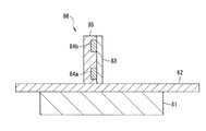
図5は、本発明の第5実施形態に係る電流測定方法の説明するための断面図である。なお、図5の第5実施形態では、被測定導体41と磁気センサ42a、42bとの位置関係に注目し、磁気センサ42a、42bを実装するプリント基板などは省略して示した。
図5において、被測定導体41上には、感磁面が互いに平行になるように複数の磁気センサ42a、42bが配置されている。ここで、左右の磁気センサ42a、42bは、被測定導体41との距離が異なっている。すなわち、被測定導体41に対して磁気センサ42aの方が磁気センサ42bに比べて距離が近いので、磁気センサ42aの電流感度の方が、磁気センサ42bの電流感度よりも大きくすることができる。そして、それらの距離の差異を大きくすると、これらの磁気センサ42a、42b間の感度差を大きくすることができ、被測定導体41に流れる電流の測定精度を向上させることができる。
FIG. 5 is a cross-sectional view for explaining a current measuring method according to the fifth embodiment of the present invention. In the fifth embodiment shown in FIG. 5, attention is paid to the positional relationship between the
In FIG. 5, a plurality of
ここで、磁気センサ42a、42bを配置する場合、被測定導体41に対する磁気センサ42a、42bの電流感度が異なるようによればよく、磁気センサ42a、42bの出力の極性は同じであっても、互いに逆であってもどちらでもかまわない。また、磁気センサ42a、42bを同一平面に配置することにより、同じ厚さを持つプリント基板やリードフレームの同一平面上に磁気センサ42a、42bを実装することができ、磁気センサ42a、42bの実装を容易化することができる。
Here, when the
図6は、本発明の第6実施形態に係る電流測定装置の概略構成を示す断面図である。なお、この第6実施形態は、図5の第5実施形態の一例に相当する。
図6において、磁気センサ56aには、基板面に平行な磁界を検出するように、基板53a上に垂直に立てられたホール素子54aが設けられ、ホール素子54aは封止材55aで封止されている。そして、ホール素子54aが設けられた磁気センサ56aはプリント基板52上に実装され、磁気センサ56aが実装されたプリント基板52はブスバー51上に配置されている。
FIG. 6 is a cross-sectional view showing a schematic configuration of a current measuring apparatus according to the sixth embodiment of the present invention. The sixth embodiment corresponds to an example of the fifth embodiment in FIG.
In FIG. 6, the
また、磁気センサ56bには、基板53b上に垂直に立てられたホール素子54bが設けられ、ホール素子54bは封止材55bで封止されている。そして、ホール素子54bが設けられた磁気センサ56bは、ホール素子54a、54bの感磁面が互いに平行になるように磁気センサ56aの横に配置されている。ここで、磁気センサ56bは、ホール素子54a、54bの感磁面が互いに平行であるならば、電流感度が得られる範囲内で任意の位置に配置することができる。
In addition, the
これにより、ブスバー51に流れる電流に起因して生成された磁場を効率よく検出させることを可能としつつ、ホール素子54a、54bの電流感度の差異に基づいてブスバー51に流れる電流を測定することが可能となるとともに、外乱磁場の影響をキャンセルさせることが可能となる。このため、磁気センサ56a、56bの配置位置およびブスバー51の形状の制約を緩和しつつ、ブスバー51に流れる電流の測定精度を向上させることが可能となる。
Accordingly, it is possible to efficiently detect the magnetic field generated due to the current flowing through the
図7は、本発明の第7実施形態に係る電流測定装置の概略構成を示す断面図である。なお、この第7実施形態は、図5の第5実施形態の一例に相当する。
図7において、磁気センサ66には、基板面に平行な磁界を検出するように、基板63a、63b上にそれぞれ垂直に立てられたホール素子64a、64bが設けられるとともに、信号処理回路63cが設けられ、ホール素子64a、64bおよび信号処理回路63cは封止材65で封止されている。そして、ホール素子64a、64bおよび信号処理回路63cが設けられた磁気センサ66はプリント基板62上に実装され、磁気センサ66が実装されたプリント基板62はブスバー61上に設置されている。ここで、磁気センサ66が実装されたプリント基板62をブスバー61上に設置する場合、ホール素子64aの直下にブスバー61を配置するとともに、ブスバー61の外部にホール素子64bが配置されるようにすることができる。
FIG. 7 is a sectional view showing a schematic configuration of a current measuring apparatus according to the seventh embodiment of the present invention. The seventh embodiment corresponds to an example of the fifth embodiment in FIG.
In FIG. 7, the
これにより、ブスバー61に流れる電流に起因して生成された磁場を効率よく検出させることを可能としつつ、ホール素子64a、64bの電流感度の差異に基づいてブスバー61に流れる電流を測定することが可能となるとともに、磁気センサ66が実装されたプリント基板62をブスバー61上に単に設置することで、外乱磁場の影響をキャンセルさせることが可能となる。このため、磁気センサ66の配置位置およびブスバー61の形状の制約を緩和しつつ、ブスバー61に流れる電流の測定精度を向上させることが可能となるとともに、ブスバー61に流れる電流の測定精度を手軽に行うことが可能となる。
Thus, it is possible to efficiently detect the magnetic field generated due to the current flowing through the
図8は、本発明の第8実施形態に係る電流測定方法の説明するための断面図である。なお、図8の第8実施形態では、被測定導体71と磁気センサ72a、72bとの位置関係に注目し、磁気センサ72a、72bを実装するプリント基板などは省略して示した。
図8において、被測定導体71上には、感磁面が互いに平行になるように複数の磁気センサ72a、72bが配置されている。ここで、一方の磁気センサ72aの被測定導体71への射影が、他方の磁気センサ72bの被測定導体71への射影と同じになるようにすることができる。
FIG. 8 is a cross-sectional view for explaining a current measuring method according to the eighth embodiment of the present invention. In the eighth embodiment shown in FIG. 8, attention is paid to the positional relationship between the conductor to be measured 71 and the
In FIG. 8, a plurality of
これにより、被測定導体71から磁気センサ72a、72bまでの距離を互いに異ならせることが可能となり、外乱磁場の影響をキャンセルさせることを可能としつつ、磁気センサ72a、72bの電流感度の差異に基づいて被測定導体71に流れる電流を測定することが可能となるとともに、磁気センサ72a、72bの組み立てを容易化することが可能となる。このため、被測定導体71に流れる電流の測定精度を向上させることが可能となるとともに、磁気センサ72a、72bの低価格化および小型化を図ることが可能となる。
As a result, the distance from the
図9は、本発明の第9実施形態に係る電流測定装置の概略構成を示す断面図である。なお、この第9実施形態は、図8の第8実施形態の一例に相当する。
図9において、磁気センサ86には、基板面に垂直な磁界を検出するように、基板83上に実装されたホール素子84a、84bが設けられ、ホール素子84a、84bは封止材85で封止されている。そして、磁気センサ86は垂直に立てられた状態でプリント基板82上に実装され、磁気センサ86が実装されたプリント基板82はブスバー81上に設置されている。
FIG. 9 is a cross-sectional view showing a schematic configuration of a current measuring apparatus according to the ninth embodiment of the present invention. The ninth embodiment corresponds to an example of the eighth embodiment in FIG.
In FIG. 9, the
ここで、ホール素子84a、84bの電流感度は、被測定導体81とホール素子84a、84bとの距離によって決めることができる。このため、被測定導体81とホール素子84a、84bとの距離を異ならせることにより、ホール素子84a、84bの電流感度の差異に基づいてブスバー81に流れる電流を測定することができる。また、ホール素子84a、84bを同一基板83上に実装することにより、ホール素子84a、84bの感磁面を互いに平行とすることができ、ホール素子84a、84bの感磁面が外乱磁場に対して同じ向きを向くようにすることができる。
Here, the current sensitivity of the
また、磁気センサ86が垂直に立てられた状態でプリント基板82上に実装することにより、ブスバー81に流れる電流によって生成された磁場をホール素子84a、84bの感磁面に効率よく貫通させることができる。また、複数のホール素子84a、84bが一体成型された磁気センサ86を用いることにより、磁気センサ86をブスバー81上に単に設置することで、ホール素子84a、84bの感磁面どうしが平行な状態を安定して維持することができる。
Further, by mounting the
このため、ブスバー81に流れる電流に起因して生成された磁場を効率よく検出させることを可能としつつ、ホール素子84a、84bの電流感度の差異に基づいてブスバー81に流れる電流を測定することが可能となるとともに、磁気センサ86が実装されたプリント基板82をブスバー81上に単に設置することで、外乱磁場の影響をキャンセルさせることが可能となる。この結果、磁気センサ86の配置位置およびブスバー81の形状の制約を緩和しつつ、ブスバー81に流れる電流の測定精度を向上させることが可能となるとともに、ブスバー81に流れる電流の測定精度を手軽に行うことが可能となる。
Therefore, the current flowing through the
図10は、本発明の第10実施形態に係る電流測定方法の説明するための断面図である。なお、図10の第10実施形態では、被測定導体91と磁気センサ92a、92bとの位置関係に注目し、磁気センサ92a、92bを実装するプリント基板などは省略して示した。
図10において、被測定導体91上には、感磁面が互いに平行になるように複数の磁気センサ92a、92bが配置されている。ここで、複数の磁気センサ92a、92bのうちの1個の磁気センサ92bは被測定導体91から十分離して配置され、被測定導体91に近接して配置された磁気センサ92aの電流感度が主となって電流を測定することができる。すなわち、磁気センサ92bの電流感度は無視できるくらい小さく、磁気センサ92bは、外乱磁場をキャンセルするためにだけのリファレンスとして用いることができる。
これにより、外乱磁場の影響による電流の測定精度の劣化を抑制しつつ、磁気センサ92bの実装位置に関する自由度を極めて高くすることができる。
FIG. 10 is a cross-sectional view for explaining a current measuring method according to the tenth embodiment of the present invention. In the tenth embodiment of FIG. 10, attention is paid to the positional relationship between the
In FIG. 10, a plurality of
As a result, it is possible to increase the degree of freedom regarding the mounting position of the
図11は、本発明の第11実施形態に係る電流測定装置の概略構成を示す断面図である。なお、この第11実施形態は、図10の第10実施形態の一例に相当する。
図11において、磁気センサ106には、基板面に平行な磁界を検出するように、基板103a、103b上にそれぞれ実装されたホール素子104a、104bが設けられている。そして、ホール素子104bが実装された基板103bは、ホール素子104aが実装された基板103a上に配置され、基板103a、103bの間で段差が構成されている。また、ホール素子104a、104bは封止材105で封止されている。そして、ホール素子104a、104bが設けられた磁気センサ106はプリント基板102上に実装され、磁気センサ106が実装されたプリント基板102はブスバー101上に設置されている。
FIG. 11 is a sectional view showing a schematic configuration of a current measuring device according to the eleventh embodiment of the present invention. The eleventh embodiment corresponds to an example of the tenth embodiment of FIG.
In FIG. 11, the
ここで、ホール素子104bが実装された基板103bをホール素子104aが実装された基板103a上に配置することにより、磁気センサ106が実装されたプリント基板102をブスバー101上に単に設置するだけで、ホール素子104a、104bの感磁面を互いに平行に保ちつつ、ブスバー101からホール素子104a、104bまでの距離を互いに異ならせることが可能となる。このため、外乱磁場の影響をキャンセルさせることを可能としつつ、磁気センサ72a、72bの電流感度の差異に基づいて被測定導体71に流れる電流を測定することが可能となり、ブスバー61に流れる電流の測定精度を向上させることが可能となる。
また、特殊に形状にフォーミングした基板を使うことにより、ホール素子104a、104bの実装位置に段差をつけた成型が可能となり、磁気センサ106の組み立てを容易化することが可能となる。
Here, by placing the
Further, by using a specially formed substrate, it is possible to mold the mounting positions of the
図12は、本発明の第12実施形態に係る電流測定方法の説明するための断面図である。なお、図12の第12実施形態では、被測定導体111と磁気センサ112a、112bとの位置関係に注目し、磁気センサ112a、112bを実装するプリント基板などは省略して示した。
図12において、被測定導体111上には、感磁面が互いに平行になるように複数の磁気センサ112a、112bが配置されている。ここで、被測定導体111は磁気センサ112a、112bの間に挟み込まれるとともに、磁気センサ112a、112bは、被測定導体111から磁気センサ112a、112bまでの距離が互いに異なるように配置することができる。
FIG. 12 is a cross-sectional view for explaining a current measuring method according to the twelfth embodiment of the present invention. In the twelfth embodiment of FIG. 12, attention is paid to the positional relationship between the
In FIG. 12, a plurality of
これにより、外乱磁場の影響をキャンセルさせることを可能としつつ、磁気センサ112a、112bの電流感度の差異に基づいて被測定導体111に流れる電流を測定することが可能となり、被測定導体111に流れる電流の測定精度を向上させることが可能となるとともに、磁気センサ112a、112bの配置の自由度を向上させることが可能となる。
As a result, it is possible to measure the current flowing through the conductor to be measured 111 based on the difference in current sensitivity between the
図13は、本発明の第13実施形態に係る電流測定装置の概略構成を示す断面図である。なお、この第13実施形態は、図12の第12実施形態の一例に相当する。
図13において、磁気センサ126aには、基板123a上に垂直に立てられたホール素子124aが設けられ、ホール素子124aは封止材125aで封止されている。そして、ホール素子124aが設けられた磁気センサ126aはプリント基板122a上に実装されている。
FIG. 13: is sectional drawing which shows schematic structure of the electric current measurement apparatus which concerns on 13th Embodiment of this invention. The thirteenth embodiment corresponds to an example of the twelfth embodiment of FIG.
In FIG. 13, the
また、磁気センサ126bには、基板123b上に垂直に立てられたホール素子124bが設けられ、ホール素子124bは封止材125bで封止されている。そして、ホール素子124bが設けられた磁気センサ126bはプリント基板122b上に実装されている。
そして、磁気センサ126a、126bがそれぞれ設けられたプリント基板122a、122bは、ブスバー121を挟み込むようにしてブスバー121の上下に配置されている。 SHAPE \* MERGEFORMAT ここで、磁気センサ126a、126bは、ホール素子124a、124bの感磁面が互いに平行であるならば、電流感度が得られる範囲内で任意の位置に配置することができる。
In addition, the
The printed
これにより、ブスバー121に流れる電流に起因して生成された磁場を効率よく検出させることを可能としつつ、ホール素子124a、124bの電流感度の差異に基づいてブスバー121に流れる電流を測定することが可能となるとともに、外乱磁場の影響をキャンセルさせることが可能となる。このため、磁気センサ126a、126bの配置位置およびブスバー121の形状の制約を緩和しつつ、ブスバー121に流れる電流の測定精度を向上させることが可能となる。
Thus, it is possible to efficiently detect the magnetic field generated due to the current flowing through the
図14は、本発明の第14実施形態に係る電流測定方法の説明するための断面図である。なお、図14の第14実施形態では、被測定導体131と磁気センサ132a、132bとの位置関係に注目し、磁気センサ132a、132bを実装するプリント基板などは省略して示した。
図14において、円柱状導体131上には、感磁面が互いに平行になるように複数の磁気センサ132a、132bが配置されている。ここで、円柱状導体131から磁気センサ132a、132bまでの距離が互いに異なるように磁気センサ132a、132bを配置することができる。
FIG. 14 is a cross-sectional view for explaining a current measuring method according to the fourteenth embodiment of the present invention. In the fourteenth embodiment shown in FIG. 14, attention is paid to the positional relationship between the conductor to be measured 131 and the
In FIG. 14, a plurality of
これにより、外乱磁場の影響をキャンセルさせることを可能としつつ、磁気センサ132a、132bの電流感度の差異に基づいて円柱状導体131に流れる電流を測定することが可能となり、円柱状導体131に流れる電流の測定精度を向上させることが可能となるとともに、円柱状導体131に流れる電流を測定する場合においても、磁気センサ132a、132bの配置の自由度を向上させることが可能となる。
This makes it possible to measure the current flowing through the
図15は、本発明の第15実施形態に係る電流測定装置の概略構成を示す断面図である。
図15において、基板141上には、信号処理回路142が実装され、信号処理回路142上には、磁気収束板144a、144bが互いに所定間隔だけ隔てて配置されている。ここで、信号処理回路142の表層には、ホール素子104a、104bが埋め込まれ、磁気収束板144aの端部がホール素子143a上に配置され、磁気収束板144bの端部がホール素子143b上に配置されるようにすることができる。そして、信号処理回路142、ホール素子143a、143bおよび磁気収束板144a、144bは、封止材145で封止されている。なお、磁気収束板144a、144bは、高透磁率、軟磁性材料で構成することができる。
FIG. 15 is a sectional view showing a schematic configuration of a current measuring apparatus according to the fifteenth embodiment of the present invention.
In FIG. 15, a
そして、ホール素子143a、143bの磁気抵抗が信号処理回路142の磁気抵抗よりも小さいものとすると、磁気収束板144aに水平に入射した磁場は、磁気収束板144a内を水平に進行する。そして、磁気収束板144a内を進行した磁場は、ホール素子143aの位置で曲げられて、ホール素子143aを垂直に貫通する。そして、ホール素子143aを貫通した磁場は、ホール素子143bの方向に曲げられて、ホール素子143bを垂直に貫通する。そして、ホール素子143bを貫通した磁場は、磁気収束板144aの位置で曲げられて、磁気収束板144a内を水平に進行する。
If the magnetic resistances of the
これにより、被測定導体から発生する磁場に対してホール素子143a、143bの感磁面を平行に配置した場合においても、被測定導体から発生する磁場を効率よく検出することが可能となり、被測定導体上に磁気センサを水平に配置することを可能としつつ、被測定導体に流れる電流を精度よく測定することが可能となる。
このように、上述した実施形態によれば、幅広で厚みのある長方形状、薄板状の被測定導体(例えば、ブスバー)に、磁気センサを近接して配置する電流測定装置または方法において、2つ以上の同一磁気センサを互いに平行になるように配置することにより、外乱等の磁気に対する2つの磁気センサの磁気感度は同じであっても、電流感度を異ならせることができる。このため、その出力信号の差分を取ることによって外乱磁場をキャンセルしつつ、同時に被測定導体に流れる電流を精度よく測定することができる。
As a result, even when the magnetic sensitive surfaces of the
As described above, according to the above-described embodiment, in the current measuring apparatus or method in which the magnetic sensor is disposed close to the wide and thick rectangular or thin plate-like measured conductor (for example, bus bar), two By arranging the above same magnetic sensors so as to be parallel to each other, even if the magnetic sensitivities of the two magnetic sensors with respect to magnetism such as disturbance are the same, the current sensitivities can be made different. For this reason, the current flowing through the conductor to be measured can be accurately measured while canceling the disturbance magnetic field by taking the difference between the output signals.
この場合、磁気センサの設置条件が磁気センサの感磁面が平行ということだけなので、磁気センサの実装位置に関する自由度を広げることができる。
また、被測定導体に対して同一の特性の磁気センサを平行に配置するだけよいため、同一プリント基板等の基板に貼り付けたり、同一リードフレームや同一基板上に一体成型することにより、極めて小型な電流センサ測定装置を構成することができる。
In this case, since the installation condition of the magnetic sensor is only that the magnetic sensitive surface of the magnetic sensor is parallel, the degree of freedom regarding the mounting position of the magnetic sensor can be expanded.
In addition, since magnetic sensors with the same characteristics need only be placed in parallel with the conductor to be measured, it is extremely small by being attached to a substrate such as the same printed circuit board or integrally formed on the same lead frame or the same substrate. A simple current sensor measuring device can be configured.
また、被測定導体の位置関係が判れば、計算によって二つの電流感度を正確に算出できるので、充分に実用的な電流測定を行うことが可能となる。
また、電流感度は、二つの磁気センサの配置関係によって広い範囲で可変・調整することができ、電流感度の調整を行うことができる。また、電流感度を厳密に規定しなくとも、規定の電流を流すことによって、キャリブレーションを行えば、正確に電流感度を求めることができるため、さらに高精度な測定が可能となる。
Further, if the positional relationship of the conductor to be measured is known, the two current sensitivities can be accurately calculated by calculation, so that sufficiently practical current measurement can be performed.
Further, the current sensitivity can be varied and adjusted in a wide range depending on the arrangement relationship between the two magnetic sensors, and the current sensitivity can be adjusted. Even if the current sensitivity is not strictly defined, if calibration is performed by passing a defined current, the current sensitivity can be obtained accurately, and therefore, a more accurate measurement is possible.
また、磁気センサの感磁面が互いに平行になるように配置すればよいため、ホール素子、MR素子、コイルなどの磁気センサをプリント基板面上に実装することで、磁気センサの感磁面平行状態を容易に作り出すことができ、極めて自由度の高い部品配置設計を行うことができる。また、部品配置の制約上、被測定導体の裏面に磁気センサを設置せざるを得ない場合も、同一平面上あるいは同一パッケージ内で電流測定装置を構成することができる。 In addition, since it is only necessary to arrange the magnetic sensitive surfaces of the magnetic sensors so as to be parallel to each other, the magnetic sensors such as Hall elements, MR elements, and coils are mounted on the printed circuit board surface so that the magnetic sensitive surfaces of the magnetic sensors are parallel. A state can be easily created, and a component placement design with a very high degree of freedom can be performed. Further, even when a magnetic sensor must be installed on the back surface of the conductor to be measured due to restrictions on component arrangement, the current measuring device can be configured on the same plane or in the same package.
本発明の電流測定装置では、磁気センサを用いて被測定導体に流れる電流の大きさを測定することができ、例えば、家電の消費電力をモニタするなどの様々の用途に用いることができる。 In the current measuring device of the present invention, the magnitude of the current flowing through the conductor to be measured can be measured using a magnetic sensor, and for example, it can be used for various applications such as monitoring the power consumption of home appliances.
1 プリント基板
2a、2b、11、21、31a、31b ワンパッケージ電流センサ
3a、3b、14a、14b、23a、23b、33a、33b、42a、42b、56a、56b、66、72a、72b、86、92a、92b、106、112a、112b、126a、126b、132a、132b 磁気センサ
4a、4b 信号処理部
5、41、71、91、111 被測定導体
6 被測定導体に流れる電流が作る磁界
6a、6b 被測定導体に流れる電流が作る磁界の一部
12a 磁気センサ部
12b、24、34a、34b、63c、142 信号処理回路
13a、13b バイアス回路
15a、15b 増幅回路
16 演算処理回路
17 記憶回路
18 出力回路
22、32a、32b リードフレーム
22´、32a´、32b´ リードピン
51、61、81、101、121 ブスバー
54a、54b、64a、64b、84a、84b、104a、104b、124a、124b、143a、143b ホール素子
8、52、62、82、102、122a、122b プリント基板
25、35a、35b、55a、55b、65、85、105、125a、125b、145 封止材
53a、53b、63a、63b、83、103a、103b、123a、123b、141 基板
131 円柱状導体
144a、144b 磁気収束板
1 Printed circuit board 2a, 2b, 11, 21, 31a, 31b One package current sensor 3a, 3b, 14a, 14b, 23a, 23b, 33a, 33b, 42a, 42b, 56a, 56b, 66, 72a, 72b, 86, 92 a, 92 b, 106, 112 a, 112 b, 126 a, 126 b, 132 a, 132 b Magnetic sensor 4 a, 4 b Signal processing unit 5, 41, 71, 91, 111 Measured conductor 6 Magnetic field generated by current flowing through the measured conductor 6 a, 6 b Part of the magnetic field generated by the current flowing through the conductor to be measured 12a Magnetic sensor unit 12b, 24, 34a, 34b, 63c, 142 Signal processing circuit 13a, 13b Bias circuit 15a, 15b Amplifying circuit 16 Arithmetic processing circuit 17 Storage circuit 18 Output circuit 22, 32a, 32b Lead frame 22 ', 32a', 32b ′ Lead pin 51, 61, 81, 101, 121 Bus bar 54a, 54b, 64a, 64b, 84a, 84b, 104a, 104b, 124a, 124b, 143a, 143b Hall element 8, 52, 62, 82, 102, 122a, 122b Printed circuit board 25, 35a, 35b, 55a, 55b, 65, 85, 105, 125a, 125b, 145 Sealant 53a, 53b, 63a, 63b, 83, 103a, 103b, 123a, 123b, 141 Substrate 131 Columnar conductor 144a, 144b Magnetic converging plate
Claims (13)
前記磁気センサの電流感度の差異が反映された出力信号に基づいて、被測定導体に流れる電流の値を算出する信号処理手段とを備えることを特徴とする電流測定装置。 A plurality of magnetic sensors;
And a signal processing unit configured to calculate a value of a current flowing through the conductor to be measured based on an output signal reflecting a difference in current sensitivity of the magnetic sensor.
ホール素子と、
前記ホール素子の感磁面に対して平行に配置され、前記被測定導体に流れる電流により発生する磁場を収束させ、前記収束させた磁場の垂直成分を前記ホール素子の感磁面に導く磁気収束板とを備えることを特徴とする請求項1〜4のいずれか1項記載の電流測定装置。 The magnetic sensor is
A Hall element;
Magnetic convergence arranged parallel to the magnetic sensing surface of the Hall element, converges the magnetic field generated by the current flowing through the conductor to be measured, and guides the vertical component of the converged magnetic field to the magnetic sensing surface of the Hall element A current measuring device according to claim 1, further comprising a plate.
前記複数の磁気センサのうち2個の磁気センサの磁場感度、前記2個の磁気センサの電流感度および前記2個の磁気センサの出力信号の値に基づいて前記被測定導体に流れる電流の値を算出することを特徴とする請求項1〜5のいずれか1項記載の電流測定装置。 The signal processing means includes
Based on the magnetic field sensitivity of two magnetic sensors of the plurality of magnetic sensors, the current sensitivity of the two magnetic sensors, and the value of the output signal of the two magnetic sensors, the value of the current flowing through the conductor to be measured is calculated. The current measuring device according to claim 1, wherein the current measuring device is calculated.
前記被測定導体に流れる電流の値I[A]は、
I=(Va−Vb)/(Sa−Sb)
であることを特徴とする請求項3〜6のいずれか1項記載の電流測定装置。 When the current sensitivities of the two magnetic sensors are Sa and Sb [V / A], respectively, and the values of the output signals of the two magnetic sensors are Va and Vb [V], respectively.
The value I [A] of the current flowing through the measured conductor is
I = (Va−Vb) / (Sa−Sb)
The current measurement device according to claim 3, wherein the current measurement device is a current measurement device.
前記被測定導体に流れる既知の電流値と、その時の前記2個の磁気センサの出力信号の値に基づいて、前記2個の磁気センサの電流感度の差分(Sa−Sb)を予め算出するキャリブレーション手段をさらに備えることを特徴とする請求項7記載の電流測定装置。 The signal processing means includes
Calibration for preliminarily calculating a difference (Sa−Sb) in current sensitivity between the two magnetic sensors based on a known current value flowing through the conductor to be measured and the output signal values of the two magnetic sensors at that time. The current measuring device according to claim 7, further comprising a measuring means.
前記磁気センサからの出力信号を取り込むステップと、
前記複数の磁気センサから取り込まれた出力信号に基づいて、前記被測定導体に流れる電流の値を算出するステップとを備えることを特徴とする電流測定方法。 Arranging a plurality of magnetic sensors so that current sensitivities to currents flowing through the conductor to be measured are different from each other;
Capturing an output signal from the magnetic sensor;
Calculating a value of a current flowing through the conductor to be measured based on output signals taken from the plurality of magnetic sensors.
前記複数の磁気センサから取り込まれた出力信号に基づいて、前記被測定導体に流れる電流の値を算出するステップとをコンピュータに実行させることを特徴とする電流測定プログラム。 Capturing output signals from a plurality of magnetic sensors arranged to have different current sensitivities to the current flowing through the conductor to be measured;
A computer program for causing a computer to execute a step of calculating a value of a current flowing through the conductor to be measured based on output signals taken from the plurality of magnetic sensors.
Priority Applications (1)
| Application Number | Priority Date | Filing Date | Title |
|---|---|---|---|
| JP2004001214A JP2005195427A (en) | 2004-01-06 | 2004-01-06 | Current measurement system, current measurement method, and current measurement program |
Applications Claiming Priority (1)
| Application Number | Priority Date | Filing Date | Title |
|---|---|---|---|
| JP2004001214A JP2005195427A (en) | 2004-01-06 | 2004-01-06 | Current measurement system, current measurement method, and current measurement program |
Publications (2)
| Publication Number | Publication Date |
|---|---|
| JP2005195427A true JP2005195427A (en) | 2005-07-21 |
| JP2005195427A5 JP2005195427A5 (en) | 2007-03-08 |
Family
ID=34816802
Family Applications (1)
| Application Number | Title | Priority Date | Filing Date |
|---|---|---|---|
| JP2004001214A Pending JP2005195427A (en) | 2004-01-06 | 2004-01-06 | Current measurement system, current measurement method, and current measurement program |
Country Status (1)
| Country | Link |
|---|---|
| JP (1) | JP2005195427A (en) |
Cited By (36)
| Publication number | Priority date | Publication date | Assignee | Title |
|---|---|---|---|---|
| JP2007114115A (en) * | 2005-10-21 | 2007-05-10 | Denso Corp | Current sensor device |
| JP2007187528A (en) * | 2006-01-12 | 2007-07-26 | Denso Corp | Current sensor |
| JP2007192820A (en) * | 2006-01-19 | 2007-08-02 | Sentron Ag | Current measurement device |
| JP2009276359A (en) * | 2009-08-27 | 2009-11-26 | Toyota Motor Corp | Current detecting device |
| JP2012026727A (en) * | 2010-07-19 | 2012-02-09 | Denso Corp | Current sensor |
| WO2012029439A1 (en) * | 2010-08-31 | 2012-03-08 | アルプス・グリーンデバイス株式会社 | Current sensor |
| CN102565506A (en) * | 2010-11-18 | 2012-07-11 | 英飞凌科技股份有限公司 | Current sensor |
| JP2012141301A (en) * | 2010-12-29 | 2012-07-26 | General Electric Co <Ge> | Current measuring systems, and methods of assembling current measuring systems |
| JP2012220469A (en) * | 2011-04-14 | 2012-11-12 | Alps Green Devices Co Ltd | Current sensor |
| JP2013531802A (en) * | 2010-07-02 | 2013-08-08 | ベルキン・インターナショナル・インコーポレイテッド | System and method for monitoring power usage in buildings |
| JP2013170878A (en) * | 2012-02-20 | 2013-09-02 | Alps Green Devices Co Ltd | Current sensor |
| JP2014029340A (en) * | 2006-01-20 | 2014-02-13 | Allegro Microsystems Llc | Arrangements for integrated sensor |
| JP2014055839A (en) * | 2012-09-12 | 2014-03-27 | Toyota Industries Corp | Current detector |
| JP2014222254A (en) * | 2008-06-02 | 2014-11-27 | アレグロ・マイクロシステムズ・エルエルシー | Current sense circuit and configuration of integrated current sensor |
| WO2015133621A1 (en) * | 2014-03-07 | 2015-09-11 | 日立金属株式会社 | Amperage detector |
| WO2016006410A1 (en) * | 2014-07-07 | 2016-01-14 | アルプス・グリーンデバイス株式会社 | Current sensor |
| US9291694B2 (en) | 2010-07-02 | 2016-03-22 | Belkin International, Inc. | System and method for monitoring electrical power usage in an electrical power infrastructure of a building |
| CN105486907A (en) * | 2014-10-07 | 2016-04-13 | 英飞凌科技股份有限公司 | Current sensor |
| US9766277B2 (en) | 2009-09-25 | 2017-09-19 | Belkin International, Inc. | Self-calibrating contactless power consumption sensing |
| US10247765B2 (en) | 2007-09-18 | 2019-04-02 | Georgia Tech Research Corporation | Detecting actuation of electrical devices using electrical noise over a power line |
| CN109752586A (en) * | 2019-03-13 | 2019-05-14 | 无锡乐尔科技有限公司 | Current detection means based on PCB |
| KR20190084000A (en) * | 2018-01-05 | 2019-07-15 | 멜렉시스 테크놀로기스 에스에이 | Offset Current Sensor Structure |
| EP3667334A1 (en) * | 2018-12-12 | 2020-06-17 | Melexis Technologies SA | Current sensor |
| CN111308153A (en) * | 2018-12-12 | 2020-06-19 | 迈来芯电子科技有限公司 | Current sensor with integrated current conductor |
| US10935612B2 (en) | 2018-08-20 | 2021-03-02 | Allegro Microsystems, Llc | Current sensor having multiple sensitivity ranges |
| US11255884B2 (en) | 2018-03-20 | 2022-02-22 | Denso Corporation | Current sensor |
| WO2022065311A1 (en) * | 2020-09-23 | 2022-03-31 | 甲神電機株式会社 | Current detection device |
| WO2022153869A1 (en) * | 2021-01-13 | 2022-07-21 | 株式会社オートネットワーク技術研究所 | Battery sensing unit and bus bar module for battery |
| US11397196B2 (en) | 2018-03-20 | 2022-07-26 | Denso Corporation | Current sensor |
| US11422165B2 (en) | 2018-03-20 | 2022-08-23 | Denso Corporation | Current sensor |
| US11567108B2 (en) | 2021-03-31 | 2023-01-31 | Allegro Microsystems, Llc | Multi-gain channels for multi-range sensor |
| WO2023053792A1 (en) * | 2021-09-29 | 2023-04-06 | 株式会社村田製作所 | Electric current sensor, method for correcting same, and method for correcting plurality of electric current sensors |
| US11656249B2 (en) | 2018-03-20 | 2023-05-23 | Denso Corporation | Current sensor with shielding for noise suppression |
| WO2023116280A1 (en) * | 2021-12-21 | 2023-06-29 | 江苏多维科技有限公司 | Stepped copper-bar current measurement apparatus |
| WO2023238585A1 (en) * | 2022-06-06 | 2023-12-14 | パナソニックIpマネジメント株式会社 | Shutoff system |
| CN109752586B (en) * | 2019-03-13 | 2024-05-10 | 宁波希磁电子科技有限公司 | PCB-based current detection device |
-
2004
- 2004-01-06 JP JP2004001214A patent/JP2005195427A/en active Pending
Cited By (64)
| Publication number | Priority date | Publication date | Assignee | Title |
|---|---|---|---|---|
| JP4506641B2 (en) * | 2005-10-21 | 2010-07-21 | 株式会社デンソー | Current sensor device |
| JP2007114115A (en) * | 2005-10-21 | 2007-05-10 | Denso Corp | Current sensor device |
| JP2007187528A (en) * | 2006-01-12 | 2007-07-26 | Denso Corp | Current sensor |
| JP4531702B2 (en) * | 2006-01-12 | 2010-08-25 | 株式会社デンソー | Current sensor |
| JP2007192820A (en) * | 2006-01-19 | 2007-08-02 | Sentron Ag | Current measurement device |
| JP2014029340A (en) * | 2006-01-20 | 2014-02-13 | Allegro Microsystems Llc | Arrangements for integrated sensor |
| US10069063B2 (en) | 2006-01-20 | 2018-09-04 | Allegro Microsystems, Llc | Integrated circuit having first and second magnetic field sensing elements |
| US9859489B2 (en) | 2006-01-20 | 2018-01-02 | Allegro Microsystems, Llc | Integrated circuit having first and second magnetic field sensing elements |
| US9082957B2 (en) | 2006-01-20 | 2015-07-14 | Allegro Microsystems, Llc | Arrangements for an integrated sensor |
| JP2014132269A (en) * | 2006-01-20 | 2014-07-17 | Allegro Microsystems Llc | Arrangements for integrated sensor |
| US11119141B2 (en) | 2007-09-18 | 2021-09-14 | Georgia Tech Research Corporation | Detecting actuation of electrical devices using electrical noise over a power line |
| US10247765B2 (en) | 2007-09-18 | 2019-04-02 | Georgia Tech Research Corporation | Detecting actuation of electrical devices using electrical noise over a power line |
| JP2014222254A (en) * | 2008-06-02 | 2014-11-27 | アレグロ・マイクロシステムズ・エルエルシー | Current sense circuit and configuration of integrated current sensor |
| JP2009276359A (en) * | 2009-08-27 | 2009-11-26 | Toyota Motor Corp | Current detecting device |
| US9594098B2 (en) | 2009-09-25 | 2017-03-14 | Belkin International Inc. | Systems and methods for measuring electrical power usage in a structure and systems and methods of calibrating the same |
| US10371728B2 (en) | 2009-09-25 | 2019-08-06 | Belkin International, Inc. | Self-calibrating contactless power consumption sensing |
| US9766277B2 (en) | 2009-09-25 | 2017-09-19 | Belkin International, Inc. | Self-calibrating contactless power consumption sensing |
| CN106093554B (en) * | 2010-07-02 | 2020-03-10 | 贝尔金国际股份有限公司 | Magnetic field sensing device and method for providing the same |
| JP2013531802A (en) * | 2010-07-02 | 2013-08-08 | ベルキン・インターナショナル・インコーポレイテッド | System and method for monitoring power usage in buildings |
| US10345423B2 (en) | 2010-07-02 | 2019-07-09 | Belkin International Inc. | System and method for monitoring electrical power usage in an electrical power infrastructure of a building |
| US10459012B2 (en) | 2010-07-02 | 2019-10-29 | Belkin International, Inc. | System for monitoring electrical power usage of a structure and method of same |
| US9857449B2 (en) | 2010-07-02 | 2018-01-02 | Belkin International, Inc. | System and method for monitoring electrical power usage in an electrical power infrastructure of a building |
| US9291694B2 (en) | 2010-07-02 | 2016-03-22 | Belkin International, Inc. | System and method for monitoring electrical power usage in an electrical power infrastructure of a building |
| CN106093554A (en) * | 2010-07-02 | 2016-11-09 | 贝尔金国际股份有限公司 | Magnetic field sensing equipment and the method for offer thereof |
| JP2012026727A (en) * | 2010-07-19 | 2012-02-09 | Denso Corp | Current sensor |
| WO2012029439A1 (en) * | 2010-08-31 | 2012-03-08 | アルプス・グリーンデバイス株式会社 | Current sensor |
| JP5487403B2 (en) * | 2010-08-31 | 2014-05-07 | アルプス・グリーンデバイス株式会社 | Current sensor |
| CN102565506B (en) * | 2010-11-18 | 2016-01-20 | 英飞凌科技股份有限公司 | Current sensor |
| CN102565506A (en) * | 2010-11-18 | 2012-07-11 | 英飞凌科技股份有限公司 | Current sensor |
| JP2012141301A (en) * | 2010-12-29 | 2012-07-26 | General Electric Co <Ge> | Current measuring systems, and methods of assembling current measuring systems |
| JP2012220469A (en) * | 2011-04-14 | 2012-11-12 | Alps Green Devices Co Ltd | Current sensor |
| JP2013170878A (en) * | 2012-02-20 | 2013-09-02 | Alps Green Devices Co Ltd | Current sensor |
| JP2014055839A (en) * | 2012-09-12 | 2014-03-27 | Toyota Industries Corp | Current detector |
| WO2015133621A1 (en) * | 2014-03-07 | 2015-09-11 | 日立金属株式会社 | Amperage detector |
| JPWO2015133621A1 (en) * | 2014-03-07 | 2017-04-06 | 日立金属株式会社 | Current detector |
| WO2016006410A1 (en) * | 2014-07-07 | 2016-01-14 | アルプス・グリーンデバイス株式会社 | Current sensor |
| US10241137B2 (en) | 2014-07-07 | 2019-03-26 | Alps Alpine Co., Ltd. | Current sensor having electromagnetic shield |
| JPWO2016006410A1 (en) * | 2014-07-07 | 2017-04-27 | アルプス電気株式会社 | Current sensor |
| CN105486907A (en) * | 2014-10-07 | 2016-04-13 | 英飞凌科技股份有限公司 | Current sensor |
| KR20190084000A (en) * | 2018-01-05 | 2019-07-15 | 멜렉시스 테크놀로기스 에스에이 | Offset Current Sensor Structure |
| KR102528062B1 (en) | 2018-01-05 | 2023-05-02 | 멜렉시스 테크놀로기스 에스에이 | Offset Current Sensor Structure |
| JP2019120687A (en) * | 2018-01-05 | 2019-07-22 | メレクシス・テクノロジーズ・ソシエテ・アノニムMelexis Technologies Sa | Offset current sensor structure |
| US11255884B2 (en) | 2018-03-20 | 2022-02-22 | Denso Corporation | Current sensor |
| US11953526B2 (en) | 2018-03-20 | 2024-04-09 | Denso Corporation | Current sensor |
| US11656249B2 (en) | 2018-03-20 | 2023-05-23 | Denso Corporation | Current sensor with shielding for noise suppression |
| US11422165B2 (en) | 2018-03-20 | 2022-08-23 | Denso Corporation | Current sensor |
| US11397196B2 (en) | 2018-03-20 | 2022-07-26 | Denso Corporation | Current sensor |
| US10935612B2 (en) | 2018-08-20 | 2021-03-02 | Allegro Microsystems, Llc | Current sensor having multiple sensitivity ranges |
| EP3667334A1 (en) * | 2018-12-12 | 2020-06-17 | Melexis Technologies SA | Current sensor |
| US11035887B2 (en) | 2018-12-12 | 2021-06-15 | Melexis Technologies Sa | Current sensor with integrated current conductor |
| EP3671228A1 (en) * | 2018-12-12 | 2020-06-24 | Melexis Technologies SA | Current sensor with integrated current conductor |
| US11422163B2 (en) | 2018-12-12 | 2022-08-23 | Melexis Technologies Sa | Current sensor |
| FR3090120A1 (en) * | 2018-12-12 | 2020-06-19 | Melexis Technologies | CURRENT SENSOR WITH INTEGRATED CURRENT CONDUCTOR |
| US11047883B2 (en) | 2018-12-12 | 2021-06-29 | Melexis Technologies Sa | Current sensor |
| CN111308153A (en) * | 2018-12-12 | 2020-06-19 | 迈来芯电子科技有限公司 | Current sensor with integrated current conductor |
| JP2020095029A (en) * | 2018-12-12 | 2020-06-18 | メレキシス テクノロジーズ エス エーMelexis Technologies SA | Current sensor |
| CN109752586A (en) * | 2019-03-13 | 2019-05-14 | 无锡乐尔科技有限公司 | Current detection means based on PCB |
| CN109752586B (en) * | 2019-03-13 | 2024-05-10 | 宁波希磁电子科技有限公司 | PCB-based current detection device |
| WO2022065311A1 (en) * | 2020-09-23 | 2022-03-31 | 甲神電機株式会社 | Current detection device |
| WO2022153869A1 (en) * | 2021-01-13 | 2022-07-21 | 株式会社オートネットワーク技術研究所 | Battery sensing unit and bus bar module for battery |
| US11567108B2 (en) | 2021-03-31 | 2023-01-31 | Allegro Microsystems, Llc | Multi-gain channels for multi-range sensor |
| WO2023053792A1 (en) * | 2021-09-29 | 2023-04-06 | 株式会社村田製作所 | Electric current sensor, method for correcting same, and method for correcting plurality of electric current sensors |
| WO2023116280A1 (en) * | 2021-12-21 | 2023-06-29 | 江苏多维科技有限公司 | Stepped copper-bar current measurement apparatus |
| WO2023238585A1 (en) * | 2022-06-06 | 2023-12-14 | パナソニックIpマネジメント株式会社 | Shutoff system |
Similar Documents
| Publication | Publication Date | Title |
|---|---|---|
| JP2005195427A (en) | Current measurement system, current measurement method, and current measurement program | |
| JP6116061B2 (en) | Current sensor | |
| JP6477684B2 (en) | Current detector | |
| JP5906488B2 (en) | Current sensor | |
| US20120306487A1 (en) | Electrical current sensing circuit, printed circuit board assembly and electrical current sensor device with the same | |
| WO2017116615A1 (en) | Sensing apparatus for sensing current through a conductor and methods therefor | |
| WO2016194240A1 (en) | Electric current sensor | |
| CN111308154A (en) | Current sensor | |
| JP2013011469A (en) | Current sensor | |
| JP2013064663A (en) | Current sensor and assembly structure of the same | |
| US20140266180A1 (en) | Sensors, systems and methods for residual current detection | |
| JP2008039517A (en) | Current sensor | |
| WO2014192625A1 (en) | Current sensor | |
| JP2002365350A (en) | Magnetic detector | |
| JP5187538B2 (en) | Magnetic sensor | |
| JP6384677B2 (en) | Current sensor | |
| JP6820367B2 (en) | Position sensor and position sensing method | |
| CN109655767B (en) | Integrated magnetic structure | |
| JP2016148597A (en) | Current sensor | |
| JP6720295B2 (en) | Current sensor | |
| JP5877728B2 (en) | Magnetic detector | |
| JP6413317B2 (en) | Current sensor | |
| US8125217B2 (en) | Magnetoresistive array design for improved sensor-to-magnet carrier tolerances | |
| JP5678285B2 (en) | Current sensor | |
| JP3961265B2 (en) | Magnetic sensor |
Legal Events
| Date | Code | Title | Description |
|---|---|---|---|
| A621 | Written request for application examination |
Free format text: JAPANESE INTERMEDIATE CODE: A621 Effective date: 20061227 |
|
| A521 | Written amendment |
Free format text: JAPANESE INTERMEDIATE CODE: A523 Effective date: 20070123 |
|
| A977 | Report on retrieval |
Free format text: JAPANESE INTERMEDIATE CODE: A971007 Effective date: 20090402 |
|
| A131 | Notification of reasons for refusal |
Free format text: JAPANESE INTERMEDIATE CODE: A131 Effective date: 20090421 |
|
| A02 | Decision of refusal |
Free format text: JAPANESE INTERMEDIATE CODE: A02 Effective date: 20090908 |