JP2005051269A - Semiconductor processing apparatus - Google Patents
Semiconductor processing apparatus Download PDFInfo
- Publication number
- JP2005051269A JP2005051269A JP2004297773A JP2004297773A JP2005051269A JP 2005051269 A JP2005051269 A JP 2005051269A JP 2004297773 A JP2004297773 A JP 2004297773A JP 2004297773 A JP2004297773 A JP 2004297773A JP 2005051269 A JP2005051269 A JP 2005051269A
- Authority
- JP
- Japan
- Prior art keywords
- processing
- model formula
- processing result
- processing apparatus
- sensor data
- Prior art date
- Legal status (The legal status is an assumption and is not a legal conclusion. Google has not performed a legal analysis and makes no representation as to the accuracy of the status listed.)
- Pending
Links
Images


Landscapes
- Drying Of Semiconductors (AREA)
Abstract
Description
本発明は半導体処理装置に係り、特に、処理結果を予測して装置の稼働率と信頼性を向上した半導体処理装置に関する。 The present invention relates to a semiconductor processing apparatus, and more particularly to a semiconductor processing apparatus that predicts a processing result and improves the operation rate and reliability of the apparatus.
近年、半導体デバイスの寸法は微細化しており、加工の寸法精度は0.1μm以下のゲート電極を10%以下の寸法精度で加工しなければならないほど厳しくなっている。一方、熱やプラズマを用いて半導体ウエハを物理化学的に加工する半導体製造装置では、装置内部の化学反応により生成される反応生成物などが装置の内壁に付着して残留し、時間と共にウエハの処理状態を変化させる。このためウエハの処理を何枚も重ねるにつれて、ウエハ上の半導体デバイスの加工形状が徐々に変化し、性能が劣化する。 In recent years, the dimensions of semiconductor devices have been miniaturized, and the dimensional accuracy of processing has become so severe that a gate electrode of 0.1 μm or less must be processed with a dimensional accuracy of 10% or less. On the other hand, in semiconductor manufacturing equipment that physicochemically processes semiconductor wafers using heat or plasma, reaction products generated by chemical reactions inside the equipment remain attached to the inner wall of the equipment, and over time, Change the processing state. For this reason, as the number of wafer processes increases, the processing shape of the semiconductor device on the wafer gradually changes and the performance deteriorates.
この問題に対しては、通常、チャンバ内壁の付着物をプラズマによってクリーニングするか、チャンバ壁の温度を上げて付着物が付き難くするなどの対策が取られる。しかし、大抵の場合、これらの対策は完全ではなく、結局半導体デバイスの加工形状は徐々に変化してしまう。このため、加工形状が問題となる場合には、加工形状が変わる前に製造装置の部品の交換や洗浄を行わなければならない。また、前記堆積膜以外にも様々な装置状態の変動がウエハの加工形状の変動に関与する。 For this problem, usually, measures are taken such as cleaning the deposits on the inner wall of the chamber with plasma, or increasing the temperature of the chamber walls to make the deposits difficult to adhere. However, in most cases, these measures are not perfect, and as a result, the processing shape of the semiconductor device gradually changes. For this reason, when the machining shape becomes a problem, the parts of the manufacturing apparatus must be replaced or cleaned before the machining shape is changed. In addition to the deposited film, various apparatus state variations are involved in wafer shape changes.
このため、半導体製造装置内部の処理状態の変化を検出し、検出結果を半導体製造処理装置の入力にフィードバックして処理状態を一定に保つなどの工夫がなされてきた。 For this reason, a device has been devised such as detecting a change in the processing state inside the semiconductor manufacturing apparatus and feeding back the detection result to the input of the semiconductor manufacturing processing apparatus to keep the processing state constant.
プラズマ処理の変動を監視する方法は、例えば特許文献1に示されている。この公報には、プラズマ処理特性と装置の電気信号の関係式
を用いて装置性能を予測したり、プラズマの状態を診断する方法が示されている。その方法としては、3つの電気信号と装置のプラズマ処理特性との関係を表す近似式を重回帰分析により求める方法が開示されている。
A method for monitoring fluctuations in plasma processing is disclosed in
また、もう一つの例が特許文献2に示されている。この公報には、既存の複数の検出器を取り付けた一般的な検出システムを半導体製造装
置に当てはめ、その検出信号の相関信号から装置の状態を監視する方法が示されている。その相関信号を生成する方法としては、6つの電気信号の比による計算式が開示されている。
Another example is shown in
また、もう一つの例が特許文献3に示されている。この公報には、光や質量分析器の数多くの信号を取り込んで相関信号を生成し装置の状態を監視する方法が示されている。また、この相関信号を生成する方法としては主成分分析を用いる方法が示されている。
しかしながら、前記特許文献1の方法では、装置を監視するセンサデータが多種類あったときに、予測しようとする処理性能と無関係な多くの信号が説明変数に入るため重回帰分析による予測がうまくいかなくなる。また、前記特許文献2の方法は、よく知られた複数の検出手段からの複数の検出信号の相関をとった信号を診断に用いるという一般的な方法である。また、開示された相関をとる方法もいくつかの信号の比をとるという従来の方法であり、これらの方法を、多くの変動原因に応じて多様な状態を取る半導体製造装置の状態を正確に監視するシステムに適用することは困難である。
However, in the method of
前記特許文献3には、以上の方法とは異なり装置からモニタした多量のデータを主成分分析して装置状態の変動を捉えることによりプラズマの状態を監視する方法が開示されている。しかし、実際の量産に用いられる半導体製造装置では、このように一般的な統計処理の方法をあてはめるだけではうまく稼動しない。例えば、主成分がどのように変化すると処理結果がどうなるのかがわからない場合がほとんどであるからである。
Unlike the above method,
本発明はこれらの問題点に鑑みてなされたもので、さまざまな種類のデバイスを処理する半導体処理装置において、処理状態をモニタし、モニタ出力に基づき異常処理を検出あるいは処理結果を予測することにより、装置の稼働率と信頼性を向上した半導体処理装置を提供する。 The present invention has been made in view of these problems. In a semiconductor processing apparatus that processes various types of devices, the processing state is monitored, and abnormal processing is detected or a processing result is predicted based on the monitor output. The present invention provides a semiconductor processing apparatus with improved operating rate and reliability of the apparatus.
本発明は上記課題を解決するため、次のような手段を採用した。 In order to solve the above problems, the present invention employs the following means.
半導体ウエハを処理する半導体処理装置の処理状態を監視するセンサと、前記半導体処理装置により処理した半導体ウエハの処理結果の測定値を入力する処理結果入力手段と、前記センサが取得したセンサデータおよび前記測定値をもとに前記センサデータを説明変数として処理結果を予測するモデル式を生成するモデル式生成部と、前記モデル式および前記センサデータをもとに処理結果を予測する処理結果予測部と、前記予測した処理結果と予め設定した設定値を比較してそのずれを補正するように前記半導体処理装置の処理条件を制御する処理条件制御部を備えた。 A sensor for monitoring a processing state of a semiconductor processing apparatus for processing a semiconductor wafer; processing result input means for inputting a measurement value of a processing result of a semiconductor wafer processed by the semiconductor processing apparatus; sensor data acquired by the sensor; A model formula generation unit that generates a model formula for predicting a processing result using the sensor data as an explanatory variable based on a measurement value; a processing result prediction unit for predicting a processing result based on the model formula and the sensor data; And a processing condition control unit that controls the processing conditions of the semiconductor processing apparatus so as to compare the predicted processing result with a preset set value and correct the deviation.
本発明によれば、処理状態をモニタし、モニタ出力に基づき異常処理を検出あるいは処理結果を予測するので、処理装置の稼働率および信頼性を向上することができる。 According to the present invention, the processing state is monitored, and the abnormal processing is detected or the processing result is predicted based on the monitor output, so that the operating rate and reliability of the processing apparatus can be improved.
図1は、本発明の第1の実施形態に係る半導体処理装置を示す図である。図において半導体処理装置1には、処理状態を監視する処理状態監視部2が備えられている。処理状態監視部2は半導体処理装置1の中に組み込まれていてもよいし、処理装置1の外側に設置しても良い。また、ネットワークなどを介して離れた場所に設置してもよい。さらに、図2に示すように機能の一部がネットワークなどを介して分離されていてもよい。
FIG. 1 is a diagram showing a semiconductor processing apparatus according to the first embodiment of the present invention. In the figure, the
処理状態監視部2の詳細を以下に示す。まず、処理装置1におけるウエハの処理状態を監視するためのセンサ3を備える。センサ3は通常、いくつかの種類のセンサを用いる。例えば、処理装置がプラズマエッチング装置やプラズマCVD装置などである場合、前記センサ3は処理中のプラズマの発光を分光器を用いてスペクトル分解し、分解した各波長ごとの発光強度をセンサデータとして取得する。例えば、1000チャンネルのCCDアレイを有する分光器を用いたときには1000個のセンサデータを1回のサンプリングごとに取得できる。また、装置の圧力や温度、ガス流量などもセンサデータとして用いる。また、電流、電圧、インピーダンスやそれらの高調波成分などの電気的測定結果をセンサデータとして用いることができる。
Details of the processing
ウエハの処理中には適当な時間間隔でこれらのセンサデータを取得し、取得したセンサデータはセンサデータ保存部4に保存する。一方、処理の終わったウエハは、処理装置1の外部あるいは装置に組み込まれた処理結果測定器により処理結果を測定する。処理結果測定は、CDSEMによるゲート幅の測定、断面SEMによる断面形状等の加工形状の測定、あるいは加工したデバイスの電気的特性の測定である。これらの測定は、全てのウエハについて行うことは必要でなく、通常は一部のウエハを抽出して処理結果を測定すればよい。
During the processing of the wafer, these sensor data are acquired at appropriate time intervals, and the acquired sensor data is stored in the sensor
処理状態監視部2は、この処理結果の測定値を受け取るために処理結果測定値入力手段5を持つ。入力手段5は、フレキシブルディスクあるいはCDROM等の可搬媒体に記録された情報を読み取る読み取り装置とすることができる。また、有線あるいは無線のネットワーク接続装置とすることもできる。
The processing
入力手段5により受け取った処理結果の測定値は、処理結果測定値保存部6に保存する。保存部6には処理結果の測定値が各種のデバイス毎に保存されることになる。
The processing result measurement value received by the input means 5 is stored in the processing result measurement
モデル式生成部7は、センサデータ保存部4および処理結果測定値保存部6から、センサデータおよび処理結果測定値データが保存されている同種のデバイスのサンプルを取り出す。このサンプルの数が、例えば3個以上あるときセンサデータを説明変数として処理結果測定値を予測するモデル式を作成することができる。通常、このときのセンサの種類およびセンサデータの数は多数であり、予測に用いるセンサおよびセンサデータを自動的に選び出すことは困難である。特に様々なデバイスが処理される場合などでは、デバイスごとに予測に有効なセンサデータの種類は異なるので、あらかじめ予測に用いるセンサを決めておくことは
困難である。
The model formula generation unit 7 extracts samples of the same type of device in which the sensor data and the processing result measurement value data are stored from the sensor
図6は、PLS法によるモデル式生成処理を説明する図である。図6に示すように、PLS法では、予測すべきデータの変動と最も相関が強くなるような説明変数を多数のセンサデータから自動的に生成する。このとき、同時にセンサデータから説明変数を計算するための関数も得られる。 FIG. 6 is a diagram for explaining model formula generation processing by the PLS method. As shown in FIG. 6, in the PLS method, explanatory variables that have the strongest correlation with fluctuations in data to be predicted are automatically generated from a large number of sensor data. At this time, a function for calculating the explanatory variable from the sensor data is also obtained.
まず、n枚のウエハの処理結果測定値を予測対象とし、Yiでi番目のウエハの処理結果測定値を表すこととする。また、一つのウエハからm個のセンサデータを得た場合は、Sijでi番目のウエハのj番目のセンサデータを示すこととする。この場合、m個のセンサデータは同じセンサの異なる時間におけるデータでもよいし、異なるセンサからのデータであってもよい。 First, the processing result measurement value of n wafers is set as a prediction target, and the processing result measurement value of the i-th wafer is represented by Yi. When m pieces of sensor data are obtained from one wafer, the j-th sensor data of the i-th wafer is indicated by Sij. In this case, the m pieces of sensor data may be data at different times of the same sensor, or may be data from different sensors.
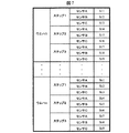
図7は、センサデータSijの例を説明する図である。図7に示すように、処理装置1の、1枚のウエハ1に対して施す処理が3ステップ(ステップ1ないしステップ3)あり、また、このとき処理状態を監視するセンサがA、B、Cの3種類であるとき、各ステップ毎の各センサのセンサデータSijを、それぞれ図に示すようにS11ないしSn9として取得する。なお、Sijは、各ステップ処理中のセンサデータの平均値としてもよいし、2乗や逆数等のセンサデータを変換した値とすることもできる。
FIG. 7 is a diagram illustrating an example of sensor data Sij. As shown in FIG. 7, the processing performed on one
PLS法を用いると、複数のセンサデータSijを、ウエハの処理結果測定値Yiの変動との相関の強さの順に並んだm個の説明変数Xikに変換することができる。センサデータSijから説明変数Xkへと変換する関数Fkは式(1)で表される。 When the PLS method is used, a plurality of sensor data Sij can be converted into m explanatory variables Xik arranged in the order of the strength of correlation with the fluctuation of the wafer processing result measurement value Yi. A function Fk for converting the sensor data Sij into the explanatory variable Xk is expressed by Expression (1).
Xik = Fk(Si1, Si2, ・・・, Sim)・・・(1)
この説明変数Xikのうちのいくつかを用いて処理結果測定値を予測する。通常は、説明変数Xi1が最も処理結果測定値Yiとの相関が強いので、Xi1,Xi2,Xi3などを説明変数として選ぶ。PLS法では式(2)のような予測式が同時に生成される。しかし、先に述べたXi1などの説明変数を用いて予測式(2)を生成した方がよいこともある。
Xik = Fk (Si1, Si2,..., Sim) (1)
A processing result measurement value is predicted using some of the explanatory variables Xik. Normally, since the explanatory variable Xi1 has the strongest correlation with the processing result measurement value Yi, Xi1, Xi2, Xi3, etc. are selected as explanatory variables. In the PLS method, a prediction formula like Formula (2) is generated simultaneously. However, it may be better to generate the prediction formula (2) using the explanatory variables such as Xi1 described above.
Yi = p(Xi1, Xi2, Xi3)・・・(2)
ところで、処理結果測定値の中には、ウエハの処理状態が悪く、異常な処理を施されたウエハの異常データも入っている。このようなデータ含めて通常の重回帰分析で予測を行うと、前記異常データに影響されて予測精度の悪いモデル式が生成される。
Yi = p (Xi1, Xi2, Xi3) (2)
By the way, the processing result measurement value includes abnormal data of a wafer which has been processed abnormally due to a bad processing state of the wafer. When prediction is performed by normal multiple regression analysis including such data, a model formula with poor prediction accuracy is generated due to the abnormal data.
図8は、ロバスト回帰分析を説明するグラフである。ロバスト回帰分析を予測に用いると、図8に示すように、異常のあるデータがアウトライアとして予測対象からはずされる。このため正しい予測モデル式を生成することができる。 FIG. 8 is a graph for explaining the robust regression analysis. When the robust regression analysis is used for prediction, as shown in FIG. 8, abnormal data is excluded from the prediction target as an outlier. Therefore, a correct prediction model formula can be generated.
図9は、モデル式生成部7のモデル式作成処理を説明するフローチャートである。モデル式生成部7において、センサデータの種類がたくさんあるときには、センサデータの主成分解析を行い(ステップ901,902)、得られた第1主成分を用いてロバスト回帰分析を行い処理結果を予測する(ステップ905〜906)。このとき、処理結果の予測に必要のない主成分も説明変数に含まれるので、回帰係数が小さい主成分を除去して(ステップ907)、別の主成分(第2主成分)を説明変数に追加(ステップ904)し、再び重回帰分析を行う(ステップ906)という処理を、予測誤差が設定値より小さくなるまで(ステップ908)繰り返し行う。予測誤差が設定値より小さくなると処理を終了する(ステップ909)。これらの回帰分析は線形でもよいし、処理の物理的特性や経験値から導かれる非線形の回帰分析を用いてもよい。
FIG. 9 is a flowchart for explaining the model formula creation process of the model formula generation unit 7. When there are many types of sensor data in the model formula generation unit 7, principal component analysis of the sensor data is performed (
このような方法で生成したモデル式は、図1に示すモデル式保存部8に保存する。モデル式は同種のデバイスごとに作成するため、モデル式保存部には処理装置1で処理するデバイスの数だけのモデル式が保存されることになる。
The model formula generated by such a method is stored in the model formula storage unit 8 shown in FIG. Since model formulas are created for each device of the same type, as many model formulas as the number of devices processed by the
処理装置1による処理が開始し、処理装置1に特定のデバイスを形成すべきウエハをロードして処理するとき、予測部9はモデル式保存部8から前記特定のデバイスに対応するモデル式をロードする。このウエハの処理中にセンサ3から得られた信号は、例えばPLS法により得られた式1を用いて説明変数に変換するか、あるいは主成分分析により主成分に変換し、式2のモデル式を用いて処理結果の予測値を計算する。計算した予測値は処理条件制御部10に渡す。処理条件制御部10は前記予測値と処理結果の設定値とのずれを補正するように処理条件
を変更する。
When processing by the
次に前記処理条件制御部10による処理条件の補正を説明する。ここで、再びPLS法を用いる。通常の半導体デバイスの処理では、加工の要求としていくつかの相反する処理性能が要求されることが多い。例えば、ゲート電極のエッチング加工などでは、ゲート電極の側壁の垂直性と下地酸化膜と、ゲートポリシリコンのエッチング選択性が要求される。
すなわち、側壁の垂直性を改善するためには堆積性の低いエッチング条件を用いたほうがよく、下地酸化膜との高選択性を達成するためには堆積性の高いエッチング条件を用いたほうがよい。このように二つの相反する要求がある場合には処理条件の制御は難しい。
図10,11,12は、このような相反する要求を満足する処理条件を求める方法を説明する図である。
Next, correction of processing conditions by the processing
That is, in order to improve the verticality of the sidewall, it is better to use etching conditions with low deposition properties, and in order to achieve high selectivity with the base oxide film, it is better to use etching conditions with high deposition properties. Thus, when there are two conflicting requirements, it is difficult to control the processing conditions.
10, 11, and 12 are diagrams for explaining a method for obtaining processing conditions that satisfy such conflicting requirements.
例えば、処理装置1の経時変化により側壁の垂直性が悪くなったときに、処理条件1(ここではガスAの流量)を減少させると垂直性が良くなるとしても、同時に下地酸化膜の選択性が悪くなる場合は処理条件としては好ましくない。
For example, when the verticality of the sidewall is deteriorated due to the change of the
このため、例えば、処理条件1と処理条件2(ここではウエハバイアス電力)を組み合わせ、側壁の垂直性を改善しながら、かつ、下地酸化膜の選択性が悪化しない条件を見出さなければならない。
For this reason, for example, it is necessary to combine the
このためには、まず、図10に示すように、通常の処理条件(中心条件)の周りに数点から数十点の処理条件を変えた実験条件を設定して加工処理を行い、処理結果を測定する。図12中の点1〜4は、図10の実験条件1〜4にあたる。ここでは処理結果測定値Aとして側壁の垂直性の測定値をとり、処理結果測定値Bとして下地酸化膜選択比をとる。
For this purpose, first, as shown in FIG. 10, processing conditions are set by setting experimental conditions in which several to several tens of processing conditions are changed around normal processing conditions (central conditions), and processing results are obtained. Measure.
次に、図11に示すように、以上の実験に対してPLS法を適用し、二種類の処理条件と二種類の処理結果測定値の相関を調べる。そうすると、図12に示すように側壁垂直性に相関の強い条件の方向Aが得られる。また、同様にしてPLS法により得られる下地酸化膜選択比に相関の強い方向から、方向Aに直交し下地酸化膜選択比に相関の強い方向Bが計算できる。この条件方向Aと条件方向Bを、図1に示す処理条件制御部10に設定しておく。このように設定しておけば、モデル式をもとに予測部9が側壁の垂直性が悪化していると予測したとき、処理条件を条件方向Aに振れば下地酸化膜選択比を犠牲にせずに側壁垂直性のみを改善することができる。計算した処理条件の制御方向は、制御条件制御部10の処理条件制御方向保存手段14に保存しておき、モデル式による処理結果予測値が設定値からずれた場合に処理条件を修正するのに用いる。
Next, as shown in FIG. 11, the PLS method is applied to the above experiment, and the correlation between the two types of processing conditions and the two types of processing result measured values is examined. Then, as shown in FIG. 12, a direction A having a strong correlation with the side wall perpendicularity is obtained. Similarly, a direction B perpendicular to the direction A and having a strong correlation with the base oxide film selection ratio can be calculated from a direction having a strong correlation with the base oxide film selection ratio obtained by the PLS method. The condition direction A and the condition direction B are set in the processing
以上の例では、二種類の処理条件を変化させたが、PLS法ではさらに多くの種類の処理条件を変化させることができ、多くの処理条件を変化させるほど好ましい結果が得られる。また、相反する処理結果測定値も、二種類だけでなく、もっと多数の処理結果を対象とすることができる。例えば、側壁の垂直性と下地酸化膜選択比に加えて、マスク選択比などを対象とすることができる。 In the above example, two types of processing conditions are changed. However, in the PLS method, more types of processing conditions can be changed, and a more favorable result is obtained as more processing conditions are changed. In addition, not only two types of conflicting processing result measurement values but also a larger number of processing results can be targeted. For example, in addition to the verticality of the side wall and the base oxide film selection ratio, the mask selection ratio can be targeted.
図3は、本発明の他の実施形態を示す図である。図において、11は予測値表示部であり、予測値、あるいは該予測値と予め設定した設定値とのずれを警告表示する。なお、図において図1に示される部分と同一部分については同一符号を付してその説明を省略する。なお、前記表示部は、警報を発するブザーあるいは電子メール等の発信手段とすることができる。 FIG. 3 is a diagram showing another embodiment of the present invention. In the figure, 11 is a predicted value display unit, which displays a predicted value or a deviation between the predicted value and a preset value. In the figure, the same parts as those shown in FIG. The display unit can be a sending means such as a buzzer for issuing an alarm or an e-mail.
図4は、本発明のさらに他の実施形態を示す図である。以上の説明では、モデル式が生成されていることを前提に処理条件制御部10の監視制御を説明した。しかし、モデル式を未だ生成していない種類のデバイスに対しては監視制御することができない。処理結果の測定には非常に時間がかかる場合が多く、ほとんど処理結果の測定が行われない場合があり、そのようなデバイスに対してはモデル式を生成することができない。図4は、このような場合でも監視制御することのできる処理状態監視部(副処理状態監視部)2’を示す図である。
FIG. 4 is a diagram showing still another embodiment of the present invention. In the above description, the monitoring control of the processing
図4に示すように、多数のセンサ3からの多種のセンサデータをもとに主成分抽出部12で主成分を抽出する。異常監視部13は前記抽出した主成分の変動のばらつきを監視することにより処理の異常を検出する。異常を検出した場合には次のウエハ処理の着手を停止すると良い。異常の検出には、例えばSPC(Statistical Process Control)と呼ばれるばらつきの管理方法を用いればよい。このためには、該当するデバイスの処理中の主成分の平均値と分散を記憶しておき、測定された主成分が平均値から分散の数倍以上離れたときに処理を異常と判定す
る。
As shown in FIG. 4, the principal
図5は、処理状態監視部2および副処理状態監視部2の双方を備えた処理装置に好適な処理フローを説明する図である。まず、処理しようとするデバイスに対するモデル式を生成し保存しているか否かを判定する(ステップ501)。モデル式が保存されている場合は処理状態監視部2により監視制御を実行する(ステップ502)。モデル式が保存されていない場合は処理状態監視部2’により監視制御を実行する(ステップ503)。
FIG. 5 is a diagram illustrating a processing flow suitable for a processing apparatus including both the processing
1 半導体処理装置
2 処理状態監視部
3 センサ
4 センサデータ保存部
5 処理結果測定値入力手段
6 処理結果測定値保存部
7 モデル式生成部
8 モデル式保存部
9 モデル式による予測部
10 処理条件制御部
11 予測値表示部
12 主成分抽出部
13 異常検出部
14 処理条件制御方向保存手段
DESCRIPTION OF
Claims (7)
前記半導体処理装置により処理した半導体ウエハの処理結果の測定値を入力する処理結果入力手段と、
前記センサが取得したセンサデータおよび前記測定値をもとに前記センサデータを説明変数として処理結果を予測するモデル式を生成するモデル式生成部と、
前記モデル式および前記センサデータをもとに処理結果を予測する処理結果予測部と、
前記予測した処理結果と予め設定した設定値を比較してそのずれを補正するように前記半導体処理装置の処理条件を制御する処理条件制御部を備えたことを特徴とする半導体処理装置。 A sensor for monitoring a processing state of a semiconductor processing apparatus for processing a semiconductor wafer;
Processing result input means for inputting a measurement value of a processing result of a semiconductor wafer processed by the semiconductor processing apparatus;
A model formula generation unit that generates a model formula for predicting a processing result using the sensor data as an explanatory variable based on the sensor data acquired by the sensor and the measurement value;
A processing result prediction unit that predicts a processing result based on the model formula and the sensor data;
A semiconductor processing apparatus, comprising: a processing condition control unit configured to control a processing condition of the semiconductor processing apparatus so as to compare the predicted processing result with a preset setting value and correct the deviation.
前記半導体処理装置により処理した半導体ウエハの処理結果の測定値を入力する処理結果入力手段と、
前記センサが取得したセンサデータおよび前記測定値をもとに前記センサデータを説明変数として処理結果を予測するモデル式を生成するモデル式生成部と、
前記モデル式および前記センサデータをもとに処理結果を予測する処理結果予測部と、
前記予測した予測値、あるいは該予測値と予め設定した設定値とのずれを表示する表示部を備えたことを特徴とする半導体処理装置。 A sensor for monitoring a processing state of a semiconductor processing apparatus for processing a semiconductor wafer;
Processing result input means for inputting a measurement value of a processing result of a semiconductor wafer processed by the semiconductor processing apparatus;
A model formula generation unit that generates a model formula for predicting a processing result using the sensor data as an explanatory variable based on the sensor data acquired by the sensor and the measurement value;
A processing result prediction unit that predicts a processing result based on the model formula and the sensor data;
A semiconductor processing apparatus, comprising: a display unit that displays the predicted value predicted or a deviation between the predicted value and a preset set value.
該抽出部が抽出した主成分の変動のばらつきをもとに処理の異常を検出する異常検出部を備え、
前記モデル式生成部にモデル式が生成されていない場合、前記異常検出部が異常を検出したとき処理を停止することを特徴とする半導体処理装置。 In Claim 1, The principal component extraction part which extracts a principal component based on a plurality of sensor data which a plurality of sensors acquired,
An abnormality detection unit that detects an abnormality in processing based on variation in fluctuation of the principal component extracted by the extraction unit,
The semiconductor processing apparatus according to claim 1, wherein when the model formula is not generated in the model formula generation unit, the process is stopped when the abnormality detection unit detects an abnormality.
Priority Applications (1)
| Application Number | Priority Date | Filing Date | Title |
|---|---|---|---|
| JP2004297773A JP2005051269A (en) | 2004-10-12 | 2004-10-12 | Semiconductor processing apparatus |
Applications Claiming Priority (1)
| Application Number | Priority Date | Filing Date | Title |
|---|---|---|---|
| JP2004297773A JP2005051269A (en) | 2004-10-12 | 2004-10-12 | Semiconductor processing apparatus |
Related Parent Applications (1)
| Application Number | Title | Priority Date | Filing Date |
|---|---|---|---|
| JP2001258116A Division JP3732768B2 (en) | 2001-08-28 | 2001-08-28 | Semiconductor processing equipment |
Related Child Applications (1)
| Application Number | Title | Priority Date | Filing Date |
|---|---|---|---|
| JP2008153133A Division JP4836994B2 (en) | 2008-06-11 | 2008-06-11 | Semiconductor processing equipment |
Publications (2)
| Publication Number | Publication Date |
|---|---|
| JP2005051269A true JP2005051269A (en) | 2005-02-24 |
| JP2005051269A5 JP2005051269A5 (en) | 2008-07-24 |
Family
ID=34270341
Family Applications (1)
| Application Number | Title | Priority Date | Filing Date |
|---|---|---|---|
| JP2004297773A Pending JP2005051269A (en) | 2004-10-12 | 2004-10-12 | Semiconductor processing apparatus |
Country Status (1)
| Country | Link |
|---|---|
| JP (1) | JP2005051269A (en) |
Cited By (6)
| Publication number | Priority date | Publication date | Assignee | Title |
|---|---|---|---|---|
| JP2007243015A (en) * | 2006-03-10 | 2007-09-20 | Hitachi Kokusai Electric Inc | Substrate processing apparatus |
| JP2007242809A (en) * | 2006-03-07 | 2007-09-20 | Toshiba Corp | Control method of semiconductor manufacturing method and control system of semiconductor manufacturing device |
| JP2009099960A (en) * | 2007-09-25 | 2009-05-07 | Toshiba Corp | Quality control method, manufacturing method of semiconductor device, and quality control system |
| WO2014065269A1 (en) * | 2012-10-24 | 2014-05-01 | 東京エレクトロン株式会社 | Correction value computation device, correction value computation method, and computer program |
| CN109643671A (en) * | 2016-08-26 | 2019-04-16 | 应用材料公司 | Self-regeneration formula semiconductor wafer processing |
| KR20190087940A (en) * | 2018-01-17 | 2019-07-25 | 가부시키가이샤 히다치 하이테크놀로지즈 | Plasma processing apparatus |
Citations (1)
| Publication number | Priority date | Publication date | Assignee | Title |
|---|---|---|---|---|
| JPH10125660A (en) * | 1996-08-29 | 1998-05-15 | Fujitsu Ltd | Plasma processor, process monitoring method and fabrication of semiconductor device |
-
2004
- 2004-10-12 JP JP2004297773A patent/JP2005051269A/en active Pending
Patent Citations (1)
| Publication number | Priority date | Publication date | Assignee | Title |
|---|---|---|---|---|
| JPH10125660A (en) * | 1996-08-29 | 1998-05-15 | Fujitsu Ltd | Plasma processor, process monitoring method and fabrication of semiconductor device |
Cited By (10)
| Publication number | Priority date | Publication date | Assignee | Title |
|---|---|---|---|---|
| JP2007242809A (en) * | 2006-03-07 | 2007-09-20 | Toshiba Corp | Control method of semiconductor manufacturing method and control system of semiconductor manufacturing device |
| JP2007243015A (en) * | 2006-03-10 | 2007-09-20 | Hitachi Kokusai Electric Inc | Substrate processing apparatus |
| JP2009099960A (en) * | 2007-09-25 | 2009-05-07 | Toshiba Corp | Quality control method, manufacturing method of semiconductor device, and quality control system |
| WO2014065269A1 (en) * | 2012-10-24 | 2014-05-01 | 東京エレクトロン株式会社 | Correction value computation device, correction value computation method, and computer program |
| JP5877908B2 (en) * | 2012-10-24 | 2016-03-08 | 東京エレクトロン株式会社 | Correction value calculation apparatus, correction value calculation method, and computer program |
| CN109643671A (en) * | 2016-08-26 | 2019-04-16 | 应用材料公司 | Self-regeneration formula semiconductor wafer processing |
| CN109643671B (en) * | 2016-08-26 | 2023-06-06 | 应用材料公司 | Self-repairing semiconductor wafer processing |
| KR20190087940A (en) * | 2018-01-17 | 2019-07-25 | 가부시키가이샤 히다치 하이테크놀로지즈 | Plasma processing apparatus |
| KR102100210B1 (en) * | 2018-01-17 | 2020-04-14 | 주식회사 히타치하이테크 | Plasma processing apparatus |
| US11289313B2 (en) | 2018-01-17 | 2022-03-29 | Hitachi High-Tech Corporation | Plasma processing apparatus |
Similar Documents
| Publication | Publication Date | Title |
|---|---|---|
| US6828165B2 (en) | Semiconductor plasma processing apparatus with first and second processing state monitoring units | |
| KR100446925B1 (en) | Process monitoring device for sample processing apparatus and control method of sample processing apparatus | |
| US10627788B2 (en) | Retrieval apparatus and retrieval method for semiconductor device processing | |
| US6590179B2 (en) | Plasma processing apparatus and method | |
| US7062411B2 (en) | Method for process control of semiconductor manufacturing equipment | |
| JP2018117116A (en) | Characteristic constraint method from time sequence of spectrum for controlling end point in processing | |
| TW200900921A (en) | Graphical user interface for presenting multivariate fault contributions | |
| JP3732768B2 (en) | Semiconductor processing equipment | |
| JP4836994B2 (en) | Semiconductor processing equipment | |
| JP2004355330A (en) | Diagnostic device and diagnostic method | |
| JP2005051269A (en) | Semiconductor processing apparatus | |
| KR100446926B1 (en) | Method of monitoring and/or controlling a semiconductor manufacturing apparatus and a system therefor | |
| JP4547396B2 (en) | Sample processing equipment | |
| JP6643202B2 (en) | Plasma processing apparatus and analysis method for analyzing plasma processing data | |
| KR101529827B1 (en) | Method for detecting endpoint of plasma etching | |
| IE20030437A1 (en) | A method for process control of semiconductor manufacturing equipment | |
| JP4344674B2 (en) | Plasma processing equipment | |
| TW511128B (en) | Method of monitoring and/or controlling a semiconductor manufacturing apparatus and a system therefor | |
| KR20230055609A (en) | Real time monitoring method and system for plasma appatus | |
| JP2016009720A (en) | Estimation method, and plasma processing apparatus | |
| JPH11238723A (en) | Method and apparatus for plasma processing | |
| IE83920B1 (en) | A method of fault detection in manufacturing equipment |
Legal Events
| Date | Code | Title | Description |
|---|---|---|---|
| A711 | Notification of change in applicant |
Effective date: 20060302 Free format text: JAPANESE INTERMEDIATE CODE: A711 |
|
| A521 | Written amendment |
Free format text: JAPANESE INTERMEDIATE CODE: A523 Effective date: 20080611 |
|
| A621 | Written request for application examination |
Free format text: JAPANESE INTERMEDIATE CODE: A621 Effective date: 20080611 |
|
| A977 | Report on retrieval |
Free format text: JAPANESE INTERMEDIATE CODE: A971007 Effective date: 20111130 |
|
| A131 | Notification of reasons for refusal |
Effective date: 20111206 Free format text: JAPANESE INTERMEDIATE CODE: A131 |
|
| A521 | Written amendment |
Free format text: JAPANESE INTERMEDIATE CODE: A523 Effective date: 20120120 |
|
| RD02 | Notification of acceptance of power of attorney |
Effective date: 20120125 Free format text: JAPANESE INTERMEDIATE CODE: A7422 |
|
| A02 | Decision of refusal |
Effective date: 20120221 Free format text: JAPANESE INTERMEDIATE CODE: A02 |