JP2005011990A - Scanning projection aligner, and illuminance calibrating method and aligning method thereof - Google Patents
Scanning projection aligner, and illuminance calibrating method and aligning method thereof Download PDFInfo
- Publication number
- JP2005011990A JP2005011990A JP2003174510A JP2003174510A JP2005011990A JP 2005011990 A JP2005011990 A JP 2005011990A JP 2003174510 A JP2003174510 A JP 2003174510A JP 2003174510 A JP2003174510 A JP 2003174510A JP 2005011990 A JP2005011990 A JP 2005011990A
- Authority
- JP
- Japan
- Prior art keywords
- illuminance
- optical system
- light
- scanning
- substrate
- Prior art date
- Legal status (The legal status is an assumption and is not a legal conclusion. Google has not performed a legal analysis and makes no representation as to the accuracy of the status listed.)
- Pending
Links
Images


Landscapes
- Exposure Of Semiconductors, Excluding Electron Or Ion Beam Exposure (AREA)
- Photometry And Measurement Of Optical Pulse Characteristics (AREA)
- Exposure And Positioning Against Photoresist Photosensitive Materials (AREA)
Abstract
Description
【0001】
【発明の属する技術分野】
この発明は、半導体のIC若しくは液晶表示素子の製造に用いられる走査型投影露光装置、該走査型投影露光装置の照度キャリブレーション方法及び該走査型投影露光装置を用いた露光方法に関するものである。
【0002】
【従来の技術】
従来、半導体素子又は液晶表示素子等を製造する際に、フォトレジストが塗布されているプレート(ガラスプレート、半導体ウエハ等)上の各ショット領域にマスク(レチクル、フォトマスク等)のパターン像をステップ・アンド・リピート方式で一括露光する投影露光装置(ステッパー)が多用されていた。
【0003】
近年、1つの大きな投影光学系を使用する代わりに、小さな複数の部分投影光学系を走査方向に沿って所定間隔で複数列に配置し、各部分投影光学系でそれぞれマスクパターンの一部の像をプレート上に投影露光する露光装置が提案されている(例えば特許文献1参照)。特許文献1に記載されているような露光装置における投影光学系は、反射プリズム、凹面鏡及び各レンズによって構成され、中間像を一度形成し、更に同一の光学系をもう一段備えることによってマスク上のパターンをプレート上に正立正像等倍にて投影する(例えば特許文献2及び特許文献3参照)。ここで、特許文献2に記載されている走査型投影露光装置においては、露光光としてg線とh線を使用しており、特許文献3に記載されている走査型露光装置においては、色収差を補正することができるように、露光光としてg,h,i線を使用している。
【0004】
また、マスク側のステージとプレート側のステージをキャリッジで保持し、一体的に走査方向に移動させ、大画面の走査露光を行う走査型露光装置が提案されている(例えば特許文献4及び特許文献5参照)。更に、近年の走査型露光装置においては、マスク側のステージとプレート側のステージを同期移動させることにより、マスクの像を繰り返し露光するいわゆるステップ・アンド・スキャン方式が主流になっている(例えば特許文献6参照)。
【0005】
また、近年の走査型露光装置においては、プレート上の照度を検出するためにプレートステージ上に照度センサが配置されている。例えば、プレートステージが1次元にしか移動できないために、複数の照度センサをプレートステージ上に配置して各部分投影光学系を通過した光の照度を検出する露光装置が存在する(例えば特許文献7参照)。また、プレートステージ上に配置された照度センサを2次元的に移動可能とした露光装置も存在する(例えば特許文献8及び特許文献9参照)。特許文献8に記載されている露光装置においては、各照明系内に配置された照度センサにより計測された照度とプレートステージ上に配置された1つの照度センサにより計測された照度に基づいて、プレートステージ上の照度を一定にしている。また、特許文献9に記載されている露光装置においては、オーバラップ露光領域の照度を測定し、オーバラップ露光領域の照度を一定にすることにより各投影位置での照度を一定にしている。
【0006】
【特許文献1】
特開平7−57986号公報
【特許文献2】
特開2000−187332号公報
【特許文献3】
特開2000−39557号公報
【特許文献4】
特開平7−283115号公報
【特許文献5】
特開平7−135165号公報
【特許文献6】
特開2000−298353号公報
【特許文献7】
特開平11−160887号公報
【特許文献8】
特開平7−153683号公報
【特許文献9】
特開平7−302753号公報
【0007】
【発明が解決しようとする課題】
しかしながら、特許文献7に開示されている露光装置のように、プレートステージ上に複数の照度センサを配置する場合、各照度センサの出力を一定とすることは可能であるが、各照度センサの感度のばらつきやフィルタ等の局所的な経年変化等により露光時の照度がばらつくといった問題が生じる。また、各計測点に応じて用いる照度センサは固定であるため、ある計測点の照度センサにゴミ等が付着した場合においても計測値に影響を与える。従って、各照度センサの計測値のばらつきが直接投影光学系にて露光される場合の照度分布に大きく影響し、一度に露光される面積内での照度むらとなる。
【0008】
一方、特許文献8に開示されている露光装置のようにプレートステージ上に1つの照度センサを配置する場合、この照度センサが経年変化等により絶対値が若干変動したとしても一度に露光される面積内で照度むらが発生することはない。従って、1つの照度センサを用いた方が精度的には良いが、計測点が増大することから計測時間が大幅に増大する。
【0009】
この発明の課題は、短時間での照度計測を可能とすることによる高スループットを実現し、かつ照度むらが生じにくい高精度な走査型投影露光装置、該走査型投影露光装置の照度キャリブレーション方法及び該走査型投影露光装置を用いた露光方法を提供することである。
【0010】
【課題を解決する為の手段】
請求項1に記載の走査型投影露光装置は、光源から射出される光束により第1の基板を照明する照明光学系と、前記第1の基板のパターンの一部の像を第2の基板上にそれぞれ投影する複数の部分投影光学系と、前記第1の基板を載置する第1のステージと、前記第2の基板を載置する第2のステージとを備え、前記第1のステージと前記第2のステージとを走査方向に同期移動させて走査露光を行う走査型投影露光装置において、前記第2のステージ上に配置され、前記照明光学系及び前記部分投影光学系を通過した光の光量又は照度を計測する複数の光電センサと、前記複数の光電センサ間の感度校正を行う感度校正手段と、前記照明光学系及び前記部分投影光学系の内の少なくとも一方に備えられ、前記複数の光電センサによる計測値に基づいて前記照明光学系及び前記部分投影光学系を通過する光の光量又は照度を調整する照度調整手段とを備え、前記感度校正手段による前記複数の光電センサ間の感度校正を前記複数の光電センサの個数よりも少ない回数の前記複数の光電センサによる計測に基づいて行うことを特徴とする。
【0011】
また、請求項2に記載の走査型投影露光装置は、前記複数の光電センサによる計測回数が2回であることを特徴とする。
【0012】
この請求項1及び請求項2に記載の走査型投影露光装置によれば、該走査型投影露光装置に設けられた複数の光電センサ間の感度校正を該複数の光電センサの個数よりも少ない回数の計測により行なうことができるため、短時間で光電センサ間の感度校正を行なうことができる。従って、照度むらが生じにくい高精度かつ高スループットの走査型投影露光装置を提供することができる。
【0013】
また、請求項3に記載の走査型投影露光装置は、前記複数の光電センサが走査方向を横切る方向に略等ピッチで配置され、前記感度校正手段による前記複数の光電センサ間の感度校正時における前記複数の光電センサによる第1回目の光量又は照度の計測後に少なくとも1ピッチ分前記第2のステージを走査方向を横切る方向に移動させて第2回目の光量又は照度の計測を行なうことを特徴とする。
【0014】
この請求項3に記載の走査型投影露光装置によれば、第1回目の光量又は照度の計測後に少なくとも1ピッチ分前記第2のステージを走査方向を横切る方向に移動させて第2回目の光量又は照度の計測を行なう、即ち、1つの計測点を2つの光電センサにより計測を行なうことにより短時間で複数の光電センサ間の感度校正を行なうことができる。
【0015】
また、請求項4に記載の走査型投影露光装置は、前記複数の光電センサ間の感度校正が前記第1の基板の交換時に行われることを特徴とする。
【0016】
この請求項4に記載の走査型投影露光装置によれば、複数の光電センサ間の感度校正が第1の基板の交換時に行われることにより、スループットを低下させることなく複数の光電センサ間の感度校正を行なうことができる。
【0017】
また、請求項5に記載の走査型投影露光装置は、光源から射出される光束により第1の基板を照明する照明光学系と、前記第1の基板のパターンの一部の像を第2の基板上にそれぞれ投影する複数の部分投影光学系と、前記第1の基板を載置する第1のステージと、前記第2の基板を載置する第2のステージとを備え、前記第1のステージと前記第2のステージとを走査方向に同期移動させて走査露光を行う走査型投影露光装置において、前記第2のステージ上に配置され、前記照明光学系及び前記部分投影光学系を通過した光の光量又は照度を計測する複数の光電センサと、前記照明光学系及び前記部分投影光学系の内の少なくとも一方に備えられ、前記複数の光電センサによる計測値に基づいて前記照明光学系及び前記部分投影光学系を通過する光の光量又は照度を調整する照度調整手段とを備え、前記部分投影光学系は、前記走査方向を横切る方向に所定間隔をもって第1列として複数配置されると共に前記走査方向を横切る前記方向に所定間隔をもって第2列として複数配置され、前記第1列の前記部分投影光学系に対応した露光領域と前記第2列の前記部分投影光学系に対応した露光領域とは、走査露光することによるオーバラップ露光領域を有し、前記照度調整手段は、前記複数の光電センサにより同時に計測された少なくとも2個所の前記オーバラップ露光領域の計測値に基づいて、前記照明光学系及び前記部分投影光学系を通過する光の光量又は照度を調整することを特徴とする。
【0018】
また、請求項6に記載の走査型投影露光装置は、前記複数の光電センサが前記第1列の前記部分投影光学系に対応した露光領域の前記オーバラップ露光領域及び前記第2列の前記部分投影光学系に対応した露光領域の前記オーバラップ露光領域の内の少なくとも一方の2個所の前記オーバラップ露光領域を同時に計測することを特徴とする。
【0019】
この請求項5及び請求項6に記載の走査型投影露光装置によれば、複数の光電センサにより同時に少なくとも2個所のオーバラップ露光領域の光量又は照度を計測するため、1つの光電センサを備える露光装置と比較して短時間に照明光学系及び部分投影光学系を通過する光の光量又は照度を調整することができる。従って、照度むらが生じにくい高精度かつ高スループットの走査型投影露光装置を提供することができる。
【0020】
また、請求項7に記載の走査型投影露光装置は、前記照明光学系が前記照明光学系から射出される光の波長を切り替える波長切り替え手段を備え、前記複数の光電センサは、前記波長切り替え手段により切り替えられた光の波長に応じた感度係数を有することを特徴とする。
【0021】
この請求項7に記載の走査型投影露光装置によれば、複数の光電センサが波長切り替え手段により切り替えられた光の波長に応じた感度係数を有しているため、光の波長毎に数種類の光電センサを設ける必要がなく、1種類の光電センサによりそれぞれの光の波長に応じた光の光量又は照度を正確に計測することができる。
【0022】
また、請求項8に記載の走査型投影露光装置は、前記照度調整手段による前記照明光学系及び前記部分投影光学系を通過した光の光量又は照度の調整が前記第1の基板の交換時に行われることを特徴とする。
【0023】
この請求項8に記載の走査型投影露光装置によれば、照明光学系及び部分投影光学系を通過した光の光量又は照度の調整が第1の基板の交換時に行われることにより、スループットを低下させることなく照明光学系及び部分投影光学系を通過した光の光量又は照度の調整を行なうことができる。
【0024】
また、請求項9に記載の走査型投影露光装置は、前記複数の光電センサが走査方向を横切る方向に略等ピッチで配置され、前記第1列の前記部分投影光学系又は前記第2列の前記部分投影光学系を通過した光の光量又は照度の計測を行う場合に、前記複数の光電センサによる第1回目の光量又は照度の計測後に少なくとも1ピッチ分、前記第2のステージを走査方向を横切る方向に移動させて第2回目の光量又は照度の計測を行なうことを特徴とする。
【0025】
この請求項9に記載の走査型投影露光装置によれば、第1回目の光量又は照度の計測後に少なくとも1ピッチ分前記第2のステージを走査方向を横切る方向に移動させて第2回目の光量又は照度の計測を行なう、即ち、1つの計測点を2つの光電センサにより計測を行なうことにより短時間で照明光学系及び部分投影光学系を通過する光の光量又は照度の調整を行なうことができる。
【0026】
また、請求項10に記載の走査型投影露光装置は、前記複数の光電センサの配置ピッチが前記部分投影光学系の配置ピッチに略等しいことを特徴とする。
【0027】
この請求項10に記載の走査型投影露光装置によれば、複数の光電センサの配置ピッチが部分投影光学系の配置ピッチに略等しいため、オーバラップ露光領域の光量又は照度を同時に計測することができ、短時間に複数の光電センサ間の感度校正及び照度調整を行なうことができる。
【0028】
また、請求項11に記載の走査型投影露光装置は、前記第1の基板を交換する位置が前記第1の基板ステージが前記第1列の前記部分投影光学系に対応した露光領域及び前記第2列の前記部分投影光学系に対応した露光領域の内の少なくとも一方の計測点を遮光しない位置とすることを特徴とする。
【0029】
この請求項11に記載の走査型投影露光装置によれば、第1の基板を交換する位置が第1の基板ステージが第1列の部分投影光学系に対応した露光領域及び第2列の部分投影光学系に対応した露光領域の内の少なくとも一方の計測点を遮光しない位置とすることにより、第1の基板の交換時に遮光されていない計測点における照明光学系及び部分投影光学系を通過する光の光量又は照度を計測することが可能となる。従って、高スループットの走査型投影露光装置を提供することができる。
【0030】
また、請求項12に記載の走査型投影露光装置は、前記照明光学系が前記光源から射出される光束に基づいて、それぞれ前記第1の基板上の一部の領域を照明する複数の部分照明光学系を備えることを特徴とする。
【0031】
この請求項12に記載の走査型投影露光装置によれば、第1の基板上の一部の領域を照明する複数の部分照明光学系を備えているため、各部分照明光学系が照度調整手段を備えることが可能となる。従って、部分照明光学系及び部分投影光学系を通過する光の光量又は照度の調整をきめ細かに行なうことができる。
【0032】
また、請求項13に記載の走査型投影露光装置の照度キャリブレーション方法は、光源から射出される光束により第1の基板を照明し、複数の部分投影光学系を用いて前記第1の基板のパターンの一部の像を第2の基板上の複数の露光領域へそれぞれ投影し、前記第1の基板と前記第2の基板とを走査方向に同期移動させて走査露光を行う走査型投影露光装置の照度キャリブレーション方法であって、前記第2の基板を載置する基板ステージ上に設けられた複数の光電センサを用いて、前記複数の露光領域の内の少なくとも2個所の光量又は照度を計測する第1計測工程と、前記第2の基板を載置する前記基板ステージを、前記複数の光電センサの配置ピッチの少なくとも1ピッチ分、前記走査方向を横切る方向に移動させる第1移動工程と、前記複数の露光領域の内の少なくとも2個所の光量又は照度を計測する第2計測工程と、前記第1計測工程及び前記第2計測工程により計測された前記照明光学系及び前記部分投影光学系を通過した光の光量又は照度に基づいて、前記複数の光電センサ間の感度を校正する感度校正工程と、前記第1計測工程及び前記第2計測工程により計測された前記照明光学系及び前記部分投影光学系を通過した光の光量又は照度に基づいて、前記照明光学系及び前記部分投影光学系を通過する光の光量又は照度を調整する照度調整工程とを含むことを特徴とする。
【0033】
この請求項13に記載の走査型投影露光装置の照度キャリブレーション方法によれば、短時間かつ高精度に複数の光電センサ間の感度校正と照明光学系及び部分投影光学系を通過する光の光量又は照度の調整を行なうことができる。
【0034】
また、請求項14に記載の走査型投影露光装置の照度キャリブレーション方法は、前記部分投影光学系が前記走査方向を横切る方向に所定間隔をもって第1列として複数配列されると共に前記走査方向を横切る前記方向に所定間隔をもって第2列として複数配置されており、前記部分投影光学系の前記第2列又は前記第1列に対応した露光領域の少なくとも2個所の光量又は照度を計測する第3計測工程とを更に含み、前記照度調整工程は、前記第1計測工程、前記第2計測工程及び前記第3計測工程により計測された前記照明光学系及び前記部分投影光学系を通過した光の光量又は照度に基づいて、前記照明光学系及び前記部分投影光学系を通過する光の光量又は照度を調整することを特徴とする。
【0035】
この請求項14に記載の走査型投影露光装置の照度キャリブレーション方法によれば、短時間かつ高精度に複数の光電センサ間の感度校正と照明光学系及び部分投影光学系を通過する光の光量又は照度の調整を行なうことができる。
【0036】
また、請求項15に記載の露光方法は、請求項1乃至請求項12の何れか一項に記載の走査型投影露光装置を用いた露光方法において、前記照明光学系を用いて前記第1の基板を照明する照明工程と、前記複数の部分投影光学系を用いて前記第1の基板のパターンの一部の像を前記第2の基板上にそれぞれ投影する投影露光工程とを含み、前記第1の基板が載置されている前記第1のステージと前記第2の基板が載置されている前記第2のステージとを同期移動させて走査露光を行うことを特徴とする。
【0037】
また、請求項16に記載の露光方法は、請求項13又は請求項14記載の走査型投影露光装置の照度キャリブレーション方法により照度のキャリブレーションを行った走査型投影露光装置を用いた露光方法において、前記照明光学系を用いて前記第1の基板を照明する照明工程と、前記複数の部分投影光学系を用いて前記第1の基板のパターンの一部の像を前記第2の基板上にそれぞれ投影する投影露光工程とを含み、前記第1の基板が載置されている前記第1のステージと前記第2の基板が載置されている前記第2のステージとを同期移動させて走査露光を行うことを特徴とする。
【0038】
この請求項15及び請求項16に記載の露光方法によれば、複数の光電センサの計測値に基づいて複数の光電センサ間の感度校正と照明光学系及び部分投影光学系を通過する光の光量又は照度の調整が短時間かつ高精度に行われた走査型投影露光装置を用いて露光を行うため、マスクパターンの転写を良好に行なうことができる。
【0039】
【発明の実施の形態】
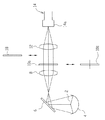
以下、図面を参照して、この発明の実施の形態について説明する。この実施の形態においては、マスク(第1の基板)Mのパターンの一部を感光性基板としてのプレート(第2の基板)Pに対して部分的に投影する複数の反射屈折型の部分投影光学系PL1〜PL7からなる投影光学系PLに対してマスクMとプレートPとを走査方向に同期移動させてマスクMに形成されたパターン像をプレートP上に走査露光するステップ・アンド・スキャン方式の走査型投影露光装置を例に挙げて説明する。
【0040】
図1は、この実施の形態にかかる走査型投影露光装置の全体の概略構成を示す斜視図である。また、図2は、この実施の形態にかかる走査型投影露光装置の光源2からライトガイドファイバ14の入射口14aまでの概略構成を示す図である。この実施の形態にかかる走査型投影露光装置は、例えば超高圧水銀ランプ光源からなる光源2を備えている。光源2より射出した光束は楕円鏡4及びダイクロイックミラー6により反射され、コリメートレンズ8に入射する。即ち、楕円鏡4の反射膜及びダイクロイックミラー6の反射膜によりg線(波長436nm)、h線(波長405nm)及びi線(波長365nm)の光を含む波長域の光が取り出され、g、h、i線の光を含む波長域の光がコリメートレンズ8に入射する。また、g、h、i線の光を含む波長域の光は、光源2が楕円鏡4の第1焦点位置に配置されているため、楕円鏡4の第2焦点位置に光源像を形成する。楕円鏡4の第2焦点位置に形成された光源像からの発散光束は、コリメートレンズ8により平行光となり、所定の露光波長域の光束のみを透過させる波長選択フィルタ10aまたは10bを透過する。
【0041】
ここで、波長選択フィルタ10aはi線の輝線近傍の光のみを透過させ、波長選択フィルタ10bはghi線の輝線近傍の光を透過させる。使用する露光波長は、必要な解像力及び露光パワーに応じて適宜選択される。即ち、投影光学系の収差が小さい場合、露光光の中心波長をλ、投影光学系の開口数をNA、プレートP上に塗布されるレジスト等によるプロセス定数をk(一般的な液晶用の工程では約0.7)とすると、解像力Rは、数式1により算出される。
【0042】
(数式1)
R = kλ/NA
また、焦点深度DOFは、数式2により算出される。
【0043】
(数式2)
DOF=λ/NA2
例えば、露光波長としてi線を用いた場合、解像力Rを3μmL/Sとし、露光光の中心波長λを365nmとすると、数式1により投影光学系の開口数NAiは0.085となり、数式2により焦点深度DOFiは約50.5μmとなる。一方、露光波長としてghi線を用いた場合、解像力Rを3μmL/Sとし、露光光の中心波長λを402nmとすると、数式1により投影光学系の開口数NAghiは0.094となり、数式2により焦点深度DOFghiは約45.5μmとなる。解像力Rを一定とした場合、露光波長としてi線を使用したときの焦点深度は、露光波長としてghi線を使用したときの焦点深度と比較すると、約1割向上する。
【0044】
また、露光波長としてi線を用いた場合、投影光学系の開口数NAは0.085とし、露光光の中心波長λを365nmとすると、数式1により解像力Riは3μmL/Sとなり、数式2により焦点深度DOFiは約50.5μmとなる。一方、露光波長としてghi線を用いた場合、投影光学系の開口数NAを0.085とし、露光光の中心波長λを402nmとすると、数式1により解像力Rghiは3.3μmL/S、数式2により焦点深度DOFghiは約55.6μmとなる。投影光学系の開口数NAを一定とした場合、露光波長としてghi線を使用したときの解像力は、露光波長としてi線を使用したときの解像力と比較すると、約1割大きい。
【0045】
例えば、約3μmL/Sの解像力を要求される液晶のTFT部において、樹脂層部分のパターンニングを行う場合には、要求される解像力は5〜10μmL/Sである。従って、低感度のレジストの使用が可能となるが、低感度のレジストを用いて良好な露光を行うためには、高い照度が必要とされる。そこで、低感度のレジストを用いる場合には、i線のみの波長を有する光を露光光として用いるより約2.5倍の照度でプレートを照明することができるghi線の波長を有する光を露光光として用いる。このようにして、解像力や露光パワーに応じて露光光に使用する波長を切り替えるために、波長選択フィルタ10aまたは10bを露光光の光路中に挿入する。
【0046】
波長選択フィルタ10aまたは10bを通過した光束は、集光レンズ12によりライトガイドファイバ14の入射口14aに集光される。ここで、ライトガイドファイバ14は、例えば多数のファイバ素線をランダムに束ねて構成されたランダムライトガイドファイバであって、入射口14a、5つの射出口14b、14d、14f、14g、14h、更に不図示の2つの射出口を備えている。ライトガイドファイバ14の入射口14aに入射した光束は、ライトガイドファイバ14の内部を伝播した後、5つの射出口14b、14d、14f、14g、14h、及び不図示の2つの射出口より分割されて射出し、マスクMを部分的に照明する複数の部分照明光学系(この実施の形態においては、7つの部分照明光学系IL1〜IL7)にそれぞれ入射する。
【0047】
なお、波長選択フィルタ10aまたは10bと集光レンズ12との間には、露光するプレートPに塗布されるレジストの感度をダイナミックに可変するための減光フィルタ機構18が配置されている。減光フィルタ機構18は、Cr等の遮光材により微小なパターンを形成しているガラス板で構成されており、光軸と直交する方向に駆動することによりパターン密度を線形的に可変し、通過する光の照度を調整する。
【0048】
また、この実施の形態においては、1つの光源を用いているが、各照明視野に応じてそれぞれ光源を有するようにしてもよい。また、多数の光源を有し、その多数の光源からの光束をランダム性の良い光ファイバ等のライトガイドファイバにより各照明視野に分割するようにしてもよい。この実施の形態においては、光源から射出された光束をライトガイドファイバ14に導く光学部材(ダイクロイックミラー6、コリメートレンズ8、波長選択フィルタ10a(10b)、集光レンズ12、減光フィルタ18)及び部分照明光学系IL1〜IL7が照明光学系を構成する。
【0049】
図3は、この実施の形態にかかる走査型投影露光装置の部分照明光学系IL1(ライトガイドファイバ14の射出口14b〜コンデンサーレンズ24b)及び部分投影光学系PL1の概略構成を示す図である。なお、部分照明光学系IL2〜IL7の構成は部分照明光学系ILと同一であり、部分投影光学系PL2〜PL7の構成は、部分投影光学系PL1の構成と同一である。
【0050】
ライトガイドファイバ14の射出口14bから射出した光束は、ライトガイドファイバ14の射出口14bの近傍に配置されている光を遮光するためのモジュールシャッタ15bを通過し、コリメートレンズ16bにより平行光にされる。
【0051】
なお、モジュールシャッタ15bとコリメートレンズ16bとの間には、部分照明光学系IL1及び部分投影光学系PL1を通過する光の照度を微調整することができるモジュール照度可変機構20bが配置されている。モジュール照度可変機構20bは、Cr等の遮光材により微小なパターンを形成しているガラス板で構成されており、光軸と直交する方向に駆動することによりパターン密度を線形的に可変し、通過する光の照度を調整する。
【0052】
コリメートレンズ16bにより集光された光束は、オプティカルインテグレータであるフライアイレンズ22bに入射する。ここで、フライアイレンズ22bは、多数の正レンズエレメントをその中心軸線が光軸に沿って伸びるように縦横に且つ稠密に配列することにより構成されている。従って、フライアイレンズ22bに入射した光束は、多数のレンズエレメントにより波面分割され、その後側焦点面(射出面近傍)にレンズエレメントの数と同数の光源像からなる二次光源を形成する。即ち、フライアイレンズ22bの後側焦点面には、実質的な面光源が形成される。フライアイレンズ22bの後側焦点面に形成された多数の二次光源からの光束は、コンデンサーレンズ24bによりマスクMをほぼ均一に照明する。
【0053】
ここで、フライアイレンズ22bとコンデンサーレンズ24bとの間には、僅かに光を反射するハーフミラー26bが配置されている。ハーフミラー26bにより反射された光は、レンズ28bを介して照明光の照度を計測する照明系内照度センサ30bに入射する。照明系内照度センサ30bは、ほぼプレートPと共役な位置に配置されており、モジュールシャッタ15bの開閉のチェック、モジュール照度可変機構20bの位置の照度チェック、露光中の照度コントロールや照度モニタに用いられる。なお、照明系内照度センサは、他の部分照明光学系IL2〜IL7のそれぞれに備えられており、照明系内照度センサ30bと同様に、それぞれの部分照明光学系IL2〜IL7のモジュールシャッタの開閉チェック、それぞれの部分照明光学系IL2〜IL7のモジュール照度可変機構の位置の照度チェック、露光中の照度コントロールや照度モニタに用いられる。
【0054】
マスクMの照明領域、即ち部分照明光学系IL1に対応する照明領域からの光は、各照明領域に対応するように配列されマスクMのパターンの一部の像をプレートP上にそれぞれ投影する複数の部分投影光学系(この実施の形態においては、7つの部分投影光学系PL1〜PL7)のうち、部分投影光学系PL1に入射する。即ち、プリズムミラー32b、屈折レンズ系34bを透過し、光学系の瞳面に配置された凹面鏡36bにより反射され、再び屈折レンズ系34bを透過し、プリズムミラー32bで反射され、視野絞り38b上に部分投影光学系PL1の中間像を形成する。更に、中間像までの光学系とほぼ同一の光学系を有する下側の光学系へと進み、プリズムミラー40b、屈折レンズ系42b、凹面鏡44b、屈折レンズ系42b、プリズムミラー40bを介して、プレートP上にマスクMのパターン像を結像する。この時の像は正立正像である。
【0055】
なお、部分照明光学系IL2〜IL7を通過した光は、各部分照明光学系IL2〜IL7のそれぞれに設けられているコンデンサーレンズによりマスクMをほぼ均一に照明し、部分照明光学系IL2〜IL7に対応して設けられている部分投影光学系PL2〜PL7に入射する。それぞれの部分投影光学系PL2〜PL7を透過した光は、プレートP上にマスクMのパターン像をそれぞれ結像する。
【0056】
ここで、マスクMはマスクホルダー(図示せず)にて固定されており、マスクステージ(第1のステージ、図示せず)に載置されている。また、マスクステージにはレーザ干渉計(図示せず)が配置されており、マスクステージレーザ干渉計はマスクステージの位置を計測及び制御する。また、プレートPはプレートホルダー(図示せず)にて固定されており、プレートステージ(第2のステージ、図示せず)に載置されている。また、プレートステージには移動鏡50(図1)が設けられている。移動鏡50には、図示していないプレートステージレーザ干渉計から射出されるレーザ光が入反射する。その入反射されたレーザ光の干渉に基づいてプレートステージの位置は計測及び制御されている。
【0057】
上述の部分照明光学系IL1、IL3、IL5、IL7は、走査方向と直交する方向(走査方向を横切る方向)に所定間隔をもって第1列として配置されており、部分照明光学系IL1、IL3、IL5、IL7に対応して設けられている部分投影光学系PL1、PL3、PL5、PL7も同様に走査方向と直交する方向に所定間隔をもって第1列として配置されている(第1列の部分投影光学系)。また、部分照明光学系IL2、IL4、IL6は、走査方向と直交する方向に所定間隔をもって第2列として配置されており、部分照明光学系IL2、IL4、IL6に対応して設けられている部分投影光学系PL2、PL4、PL6も同様に走査方向と直交する方向に所定間隔をもって第2列として配置されている(第2列の部分投影光学系)。第1列の部分投影光学系と第2列の部分投影光学系との間には、プレートPの位置合わせを行うために、オフアクシスのアライメント系52が配置されている。また、第1列の部分投影光学系と第2列の部分投影光学系との間には、マスクMやプレートPのフォーカスを合わせるために、オートフォーカス系54が配置されている。
【0058】
また、プレートステージ上には部分照明光学系IL1〜IL7及び部分投影光学系PL1〜PL7を通過した光の光量及び照度を計測する複数の光電センサ(この実施の形態においては、6つの照度センサI1〜I6)が配置されている。照度センサI1〜I6のそれぞれは、プレートPに対してほぼ共役位置に配置されたφ0.01mm〜φ1mm程度のピンホールと、このピンホールを介した光を受光する光電センサと、ピンホールと光電センサとの間に配置される色選択フィルタとから構成されている。この6つの照度センサI1〜I6は、走査方向を横切る方向に略等ピッチで配列されている。照度センサI1〜I6の配置ピッチは、部分投影光学系PL1〜PL7の視野絞りの間隔と同一ピッチである。照度センサI1〜I6により計測された照度計測値に基づいて、減光フィルタ18又はそれぞれの部分照明光学系に設けられたモジュール照度可変機構を用いて、部分照明光学系IL1〜IL7及び部分投影光学系PL1〜PL7を通過する光の照度を調整する。
【0059】
なお、照度センサI1〜I6は、ghi線の波長に対して照度センサI1〜I6の感度とレジストの分光感度とが合致するように、照度センサI1〜I6のそれぞれに光透過率を調整するための色選択フィルタを備えている。しかしながら、単一の波長を取り出し計測した場合においては、レジストの種類による分光感度の違いまたは色選択フィルタのばらつき等により、照度センサI1〜I6の感度とレジストの分光感度に若干差が生じる。従って、照度センサI1〜I6は、予めghi線及びi線の波長に応じた感度係数を有し、照明光の波長に応じた感度係数を用いて照度計測を行う。
【0060】
図4は、この実施の形態にかかる走査型投影露光装置のシステム構成を示すブロック図である。部分照明光学系IL1に備えられている照明系内照度センサ30bによる検出値は、制御装置60に入力される。部分照明光学系IL1には、モジュール照度可変機構20bを駆動するモジュール照度可変機構駆動部62が設けられており、制御部60からモジュール照度可変機構駆動部62に対して制御信号が出力される。同様に、各照明光学系IL2〜IL7に設けられている照明系内照度センサによる検出値は制御部60に入力され、制御部60から各照明光学系IL2〜IL7に設けられているモジュール照度可変機構駆動部に対して制御信号が出力される。
【0061】
また、制御装置60には、プレートP上の照度を計測する照度センサI1〜I6が接続されており、照度センサI1〜I6により計測された照度が入力される。また、制御装置60には、プレートステージの位置合わせを行なうアライメント系52、マスクMとプレートPのフォーカス合わせを行うオートフォーカス系54、プレートPの位置計測及び制御を行うプレートステージレーザ干渉計、マスクMの位置計測及び制御を行うマスクステージレーザ干渉計が接続されている。
【0062】
また、制御装置60には、波長選択フィルタ10を駆動する波長選択フィルタ駆動部64、減光フィルタ18を駆動する減光フィルタ駆動部66、マスクステージを走査方向に移動させるマスクステージ駆動部68を制御するマスクステージ制御部70、プレートステージを走査方向または走査方向を横切る方向に移動させるプレートステージ駆動部72を制御するプレートステージ制御部74が接続されている。
【0063】
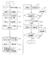
次に、図5の照度キャリブレーションの手順を示す図及び図6のフローチャートを参照して、走査型投影露光装置の照度キャリブレーション方法の手順を説明する。通常、走査型投影露光装置の照度キャリブレーションは、マスクMが投影光学系PLの視野から外れた位置にある時、若しくは、マスクMの交換時に行われる。図5(a)〜(d)に示すように、プレートP上における部分投影光学系PL1〜PL7のそれぞれによる露光領域76a〜76gは、各部分投影光学系PL1〜PL7の視野領域に対応して所定の形状に設定されており、この実施の形態においては台形形状を有している。露光領域76a、76c、76e、76gと露光領域76b、76d、76fとは、走査方向に沿って対向して形成されている。また、露光領域76a〜76gのそれぞれは、部分投影光学系PL1〜PL7が走査露光することによるオーバラップ露光領域を有する。即ち、露光領域76aは露光領域76b側の端部にオーバラップ露光領域を有し、露光領域76bは露光領域76a側及び露光領域76c側、即ち両端部にオーバラップ露光領域を有する。同様に、露光領域76c、76d、76e、76fは両端部にオーバラップ露光領域を有し、露光領域76gは露光領域76f側の端部にオーバラップ露光領域を有する。さらに、露光領域76a〜76gの継ぎ部(各露光領域の隣り合う露光領域との境界部)の走査方向における露光領域の幅とそれぞれの継ぎ部に対応する隣り合う露光領域の継ぎ部の走査方向における露光領域の幅との総計は、継ぎ部に相当しない露光領域76a〜76gの走査方向における露光領域の幅と略等しくなるように設定されている。
【0064】
なお、この実施の形態の露光領域76a〜76gの形状は台形であるが、六角形、菱形若しくは平行四辺形であっても構わない。
【0065】
また上述のように、照度センサI1〜I6は、部分投影光学系PL1〜PL7の視野絞りの間隔と同じピッチで配列されているため、露光領域76a〜76gの継ぎ部の位置の照度を計測することができる。
【0066】
まず、制御装置60は、照度センサI1〜I6により第2列の部分投影光学系の露光領域76b、76d、76fの少なくとも2個所の照度計測点(この実施の形態においては、6つの照度計測点m1〜m6)の位置の照度を計測できるように、プレートステージ制御部74を介してプレートステージ駆動部72に制御信号を出力し、プレートステージを走査方向に移動する(ステップS10)。照度計測点m1〜m6は、第2列の部分投影光学系のオーバラップ領域の継ぎ部に位置している。図5(b)は、ステップS10においてプレートステージを移動した後の照度センサI1〜I6の位置を示している。
【0067】
次に、制御装置60は、それぞれの照度センサI1〜I6により同時に計測された照度計測点m1〜m6の第1回目の照度計測値を取得する(ステップS11)。次に、制御装置60は、プレートステージ制御部74を介してプレートステージ駆動部72に制御信号を出力し、プレートステージを走査方向と直交する方向に1ピッチ分移動する(ステップS12)。図5(c)は、ステップS12においてプレートステージを移動した後の照度センサI1〜I6の位置を示している。即ち、照度計測点m2に位置していた照度センサI2が照度計測点m1の位置に、照度計測点m3に位置していた照度センサI3が照度計測点m2の位置に、照度計測点m4に位置していた照度センサI4が照度計測点m3の位置に、照度計測点m5に位置していた照度センサI5が照度計測点m4の位置に、照度計測点m6に位置していた照度センサI6が照度計測点m5の位置にそれぞれ移動する。
【0068】
なお、ステップS12において、プレートステージを走査方向と直交する方向に1ピッチ分移動させたが、プレートステージを走査方向と直交する方向に1ピッチより多いピッチ分移動させてもよい。
【0069】
次に、制御装置60は、それぞれの照度センサI2〜I6による照度計測点m1〜m5の第2回目の照度計測値を取得する(ステップS13)。ここで、ステップS13においては、照度センサI1は照度計測点m1〜m6の何れにも位置していないため、照度計測を行わない。次に、ステップS11及びステップS13においてそれぞれの照度センサI1〜I6により計測されたそれぞれの計測点m1〜m6の照度に基づいて、照度センサI1〜I6間の感度校正を行う(ステップS14)。
【0070】
ここで、予め照度センサI1に対して感度校正が施されている場合には、照度センサI1を基準照度センサとして用いる。照度センサI1により計測された計測点m1の照度と照度センサI2により計測された計測点m1に基づいて、照度センサI1の感度と同一の感度となるように照度センサI2の感度校正を行う。次に、感度校正された照度センサI2の感度、照度センサI2により計測された計測点m2の照度と照度センサI3により計測された計測点m2の照度に基づいて、照度センサI3の感度校正を行う。同様にして、照度センサI4〜I6の感度校正を行う。
【0071】
なお、この実施の形態においては、6つの照度センサを備えているが、2つ以上の照度センサを備えていればよい。また、この実施の形態においては、照度センサI1を基準照度センサとして用いているが、照度センサI2〜I6の何れか1つに対して感度校正を施しておき、感度校正を施した照度センサを基準照度センサとして用いてもよい。
【0072】
次に、制御装置60は、照度センサI1〜I6により第1列の部分投影光学系の露光領域76a、76c、76e、76gの照度計測点m7〜m12の位置の照度を計測できるように、プレートステージ制御部74を介してプレートステージ駆動部72に制御信号を出力し、プレートステージを走査方向と直交する方向に1ピッチ分移動すると共にプレートステージを走査方向に移動する(ステップS15)。図5(d)は、ステップS15においてプレートステージを走査方向と直交する方向に1ピッチ分移動すると共にプレートステージを走査方向に移動した後の照度センサI1〜I6の位置を示す図である。制御装置60は、それぞれの照度センサI2〜I6による照度計測点m7〜m12の照度計測値を取得する(ステップS16)。
【0073】
次に、制御装置60は、ステップS11及びステップS13において計測された計測点m1〜m6の照度計測値、ステップS16において計測された計測点m7〜m12の照度計測値、並びにステップS14において感度校正された照度センサI1〜I6の感度に基づいて、部分照明光学系IL1〜IL7及び部分投影光学系PL1〜PL7を通過する光の照度を調整する(ステップS17)。
【0074】
即ち、それぞれの計測点m1〜m12の照度計測値に基づいて、部分照明光学系IL1〜IL7及び部分投影光学系PL1〜PL7を通過する光の照度を全体的に調節する必要がある場合には、制御装置60は、減光フィルタ駆動部64に制御信号を出力し、減光フィルタ18を光軸と直交する方向に移動し、減光フィルタ18を通過する光の照度を調節する。また、各部分照明光学系IL1〜IL7及び各部分投影光学系PL1〜PL7を通過する光の照度を個々に調節する必要がある場合には、制御装置60は、照度調節を行う計測点に対応した部分照明光学系に設けられているモジュール照度可変機構駆動部に制御信号を出力する。制御信号を出力することにより、部分照明光学系IL1〜IL7に設けられているモジュール照度可変機構を移動し、それぞれの部分照明光学系IL1〜IL7から射出される光の照度を調節する。
【0075】
次に、制御装置60は、照度センサI1〜I6により再度計測された計測点m7〜m12の照度の計測値を取得する(ステップS18)。次に、ステップS18において取得した計測点m7〜m12の照度計測値に基づいて、ステップS17において部分照明光学系IL1、IL3、IL5、IL7及び部分投影光学系PL1、PL3、PL5、PL7を通過する光の照度調整が正確に行われた否かの判定を行う(ステップS19)。部分照明光学系IL1、IL3、IL5、IL7及び部分投影光学系PL1、PL3、PL5、PL7を通過する光の照度調整が正確に行われたと判定された場合には、制御装置60は、プレートステージ制御部74を介してプレートステージ駆動部72に制御信号を出力し、プレートステージを走査方向(第1列の部分投影光学系から第2列の部分投影光学系へ向かう方向)に移動する(ステップS20)。
【0076】
一方、ステップS19において部分照明光学系IL1、IL3、IL5、IL7及び部分投影光学系PL1、PL3、PL5、PL7を通過する光の照度調整が正確に行われていないと判定された場合には、ステップS17と同様にして、部分照明光学系IL1〜IL7及び部分投影光学系PL1〜PL7を通過する光の照度を調整し(ステップS21)、再度、計測点m7〜m12の照度の計測を行うと共に照度調整が正確に行われたか否かの判定を行う。
【0077】
次に、制御装置60は、照度センサI1〜I6により再度計測された計測点m1〜m6の計測値を取得する(ステップS22)。次に、ステップS22において取得した計測点m1〜m6の照度に基づいて、ステップS17において部分照明光学系IL2、IL4、IL6及び部分投影光学系PL2、PL4、PL6を通過する光の照度調整が正確に行われた否かの判定を行う(ステップS23)。部分照明光学系IL2、IL4、IL6及び部分投影光学系PL2、PL4、PL6を通過する光の照度調整が正確に行われたと判定された場合には、走査型投影露光装置の照度キャリブレーションの処理を終了する。一方、ステップS23において部分照明光学系IL2、IL4、IL6及び部分投影光学系PL2、PL4、PL6を通過する光の照度調整が正確に行われていないと判定された場合には、ステップS17と同様にして、部分照明光学系IL2、IL4、IL6及び部分投影光学系PL2、PL4、PL6を通過する光の照度を調整し(ステップS24)、再度、計測点m1〜m6の照度の計測を行うと共に照度調整が正確に行われたか否かの判定を行う。
【0078】
この実施の形態にかかる走査型投影露光装置によれば、複数の照度センサ間の感度校正を複数の照度センサの個数よりも少ない回数の計測により行なうことができるため、短時間で照度センサ間の感度校正を行なうことができる。また、1つの照度センサを備える露光装置と比較しても同一の精度を得ることができ、照度むらが生じにくい高精度かつ高スループットの走査型投影露光装置を提供することができる。
【0079】
また、この実施の形態にかかる走査型投影露光装置によれば、第1列の部分投影光学系のオーバラップ露光領域の照度と、その第1列の部分投影光学系のオーバラップ露光領域とオーバラップする第2列の部分投影光学系のオーバラップ露光領域の照度を同一の照度センサにより照度計測し、部分投影光学系を通過する光の照度調整を行なう。従って、照度センサ間の感度校正のための照度計測が行われている時に照度リップル等の影響を受けた場合であっても、第1列の部分投影光学系のオーバラップ露光領域の照度と、その第1列の部分投影光学系のオーバラップ露光領域とオーバラップする第2列の部分投影光学系のオーバラップ露光領域の照度を同一の照度センサで計測するため、オーバラップ露光領域部分に極端な照度差が生じることもない。
【0080】
また、上述の実施の形態にかかる走査型投影露光装置の照度キャリブレーション方法によれば、複数の照度センサを備えることにより短時間での照度センサ間の感度校正並びに部分照明光学系及び部分投影光学系を通過する光の照度調整が可能となる。即ち、通常の照度キャリブレーションによれば、照度調整後の確認のための計測を含めると、3回の走査方向に沿った移動、4回の照度計測及び1回の照度調整機構の駆動により部分投影光学系を通過する光の照度調整し、照度センサ間の感度校正は別途行う必要がある。一方、この実施の形態にかかる照度キャリブレーションによれば、照度調整後の確認のための計測を含めると、3回の走査方向に沿った移動、5回の照度計測、1回の照度調整機構駆動及び1回の走査方向と直交する方向の移動により照度センサ間の感度校正及び部分投影光学系を通過する光の照度調整を同時に行なうことができる。
【0081】
即ち、この実施の形態にかかる部分投影光学系を通過する光の照度調整には、通常の照度キャリブレーションと同様に、照度調整後の確認のための計測を含め、3回の走査方向に沿った移動、4回の照度計測及び1回の照度調整機構の駆動が必要である。また、照度センサ間の感度校正には、1回の走査方向に沿った移動、2回の照度計測、及び1回の走査方向と直交する方向の移動が必要である。照度センサ間の感度校正における1回の走査方向に沿った移動は、部分投影光学系を通過する光の照度調整における3回の走査方向に沿った移動の内の1回の走査方向に沿った移動と同一動作とすることができる。また、照度センサ間の感度校正における2回の照度計測の内の1回の照度計測は、部分投影光学系を通過する光の照度調整における4回の照度計測の内の1回の照度計測と同一動作とすることができる。従って、照度センサ間の感度校正に必要である1回の走査方向に沿った移動及び1回の照度計測に要する時間を短縮することができ、1回の照度計測及び1回の走査方向と直交する方向の移動に要する時間の増加のみで照度センサ間の感度校正を部分投影光学系を通過する光の照度調整と同時に行なうことができる。
【0082】
また、この実施の形態にかかる走査型投影露光装置の照度キャリブレーション方法においては、少なくとも2つ以上の照度センサにより1つの計測点の照度を計測するが、各照度センサにより計測された各照度計測値をそれぞれ比較し、極端に低い照度計測値を出力した照度センサがある場合、該照度センサにゴミ等が付着している可能性が考えられる。従って、予め1つの計測点に対して一方の照度センサにより計測される照度計測値と他方の照度センサにより計測される照度計測値との差を求め、その差に閾値を設けるようにしてもよい。閾値を設けることによりその閾値を越えた場合において、極端に低い照度度計測値を出力した照度センサにゴミ等が付着しているか否かの点検を行うように設定することができる。
【0083】
また、複数の照度センサを備えることにより、照度センサ間の感度校正を行う際に、それぞれの照度センサの感度、精度または劣化等の比較を容易に行なうことができ、それぞれの照度センサの精度や経年劣化の変動を早期に検出することも可能である。
【0084】
なお、この実施の形態においては、照度センサ間の感度校正と照度キャリブレーションを同時に行ったが、照度センサ間の感度校正と照度キャリブレーションを別々に行ってもよい。
【0085】
また、この実施の形態においては、第2列の部分投影光学系のオーバーラップ露光領域の継ぎ部の照度を6つの照度センサI1〜I6で計測し照度センサ間の感度校正を行なったが、第1列の部分投影光学系のオーバラップ露光領域の継ぎ部の照度を7つの照度センサで計測し照度センサ間の感度校正を行ってもよい。この場合においては、部分投影光学系PL1に対応する露光領域76aの両端部、部分投影光学系PL3に対応する露光領域76cの両端部、部分投影光学系PL5に対応する露光領域76eの両端部、部分投影光学系PL7に対応する露光領域76gの露光領域76e側の端部に位置する計測点の照度を7つの照度センサで計測する(第1回目の計測)。次に、プレートステージを走査方向と直交する方向に移動させて、露光領域76aの露光領域76c側の端部、露光領域76cの両端部、露光領域76eの両端部、露光領域76gの両端部に位置する計測点の照度を7つの照度センサで計測する(第2回目の計測)。第1回目及び第2回目の照度計測を行うことにより、部分投影光学系PL1〜PL7に対応する露光領域全ての端部における照度計測を行なうことができる。
【0086】
また、この実施の形態にかかる走査型投影露光装置の照度キャリブレーション方法において、照度キャリブレーションをマスクの交換時に行うことにより更に照度キャリブレーションに要する時間を短縮することができる。例えば、マスクの交換は通常マスクステージのストロークエンドに近い位置で行われる。マスクの交換時に、マスクステージが第1列の部分投影光学系及び第2列の部分投影光学系に対応した露光領域の内の少なくとも一方の計測点を遮光しないようにすることにより、マスクの交換にかかる受け渡し時間を照度キャリブレーション方法に要する動作時間に割り当てることができる。即ち、マスクステージがマスク交換をするために移動している間に、照度センサが最初の計測点における照度を計測できるようにプレートステージを走査方向に沿って移動させる。次にマスク交換を行っている間に、1回目の照度計測、走査方向と直交する方向の移動、及び2回目の照度計測を行なうことができればよい。この場合において、マスク交換、照度センサ間の感度校正、部分照明光学系及び部分投影光学系を通過した光の照度調整を別々に行った場合にかかる時間と比較して、大幅に時間短縮することができる。
【0087】
走査型投影露光装置の照度キャリブレーション方法をマスクの交換時に行う場合においては、時間的余裕がある場合、走査方向を横切る方向でプラス側とマイナス側にステップ移動させ、複数の照度センサにより照度計測を行うことにより全ての照度センサが照度計測値を2つ以上持つことになるため、更なる高精度な感度校正及び照度調整が可能となる。
【0088】
なお、上述の実施形態では、1つの照度センサによって計測する領域をピンホールにより規定しているが、走査方向に積算された光量を計測するために、走査方向に沿って所定の長さを有するスリットを用いても良い。ここで、スリットの走査方向に沿った長さは露光幅(露光領域の走査方向に沿った幅)よりも長く設定されることが望ましい。なお、ピンホールを用いた局所点での計測とスリットを用いた露光幅を考慮した計測とを使い分けるように構成してもかまわない。
【0089】
上述の実施の形態における露光装置では、照明装置によってレチクル(マスク)を照明し(照明工程)、投影光学系を用いてマスクに形成された転写用のパターンを感光性基板に露光する(露光工程)ことにより、マイクロデバイス(半導体素子、撮像素子、液晶表示素子、薄膜磁気ヘッド等)を製造することができる。以下、この実施の形態にかかる走査型投影露光装置を用いて感光性基板としてのウエハ等に所定の回路パターンを形成することによって、マイクロデバイスとしての半導体デバイスを得る際の手法の一例につき図7のフローチャートを参照して説明する。
【0090】
先ず、図7のステップ301において、1ロットのウエハ上に金属膜が蒸着される。次のステップ302において、その1ロットのウエハ上の金属膜上にフォトレジストが塗布される。次に、この実施の形態にかかる走査型投影露光装置の照度キャリブレーション方法に従い、それぞれの部分照明光学系及び部分投影光学系を透過した光の照度を計測し、その計測結果に基づいて照度センサ間の感度校正並びにそれぞれの部分照明光学系及び部分投影光学系を通過する光の照度調整を行なう。その後、ステップ303において、この実施の形態にかかる走査型投影露光装置を用いて、マスク上のパターンの像がその部分投影光学系を介して、その1ロットのウエハ上の各ショット領域に順次露光転写される。その後、ステップ304において、その1ロットのウエハ上のフォトレジストの現像が行われた後、ステップ305において、その1ロットのウエハ上でレジストパターンをマスクとしてエッチングを行うことによって、マスク上のパターンに対応する回路パターンが、各ウエハ上の各ショット領域に形成される。
【0091】
その後、更に上のレイヤの回路パターンの形成等を行うことによって、半導体素子等のデバイスが製造される。上述の半導体デバイス製造方法によれば、予め複数の照度センサ間の感度校正並びにそれぞれの部分照明光学系及び部分投影光学系を通過する光の照度調整が短時間かつ高精度に行われているため、良好な露光を行なうことができる。なお、ステップ301〜ステップ305では、ウエハ上に金属を蒸着し、その金属膜上にレジストを塗布、そして露光、現像、エッチングの各工程を行っているが、これらの工程に先立って、ウエハ上にシリコンの酸化膜を形成後、そのシリコンの酸化膜上にレジストを塗布、そして露光、現像、エッチング等の各工程を行っても良いことはいうまでもない。
【0092】
また、この実施の形態にかかる露光装置では、プレート(ガラス基板)上に所定のパターン(回路パターン、電極パターン等)を形成することによって、マイクロデバイスとしての液晶表示素子を得ることもできる。以下、図8のフローチャートを参照して、このときの手法の一例につき説明する。まず、この実施の形態にかかる走査型投影露光装置の照度キャリブレーション方法に従い、それぞれの部分照明光学系及び部分投影光学系を通過する光の照度を計測し、その計測結果に基づいて照度センサ間の感度校正並びにそれぞれの部分照明光学系及び部分投影光学系を通過する光の照度の調整を行なう。図8において、パターン形成工程401では、この実施の形態にかかる露光装置を用いてマスクのパターンを感光性基板に転写露光する、所謂光リソグラフィ工程が実行される。この光リソグラフィ工程によって、感光性基板上には多数の電極等を含む所定パターンが形成される。その後、露光された基板は、現像工程、エッチング工程、レジスト剥離工程等の各工程を経ることによって、基板上に所定のパターンが形成され、次のカラーフィルタ形成工程402へ移行する。
【0093】
次に、カラーフィルタ形成工程402では、R(Red)、G(Green)、B(Blue)に対応した3つのドットの組がマトリックス状に多数配列されたり、またはR、G、Bの3本のストライプのフィルタの組を複数水平走査線方向に配列されたりしたカラーフィルタを形成する。そして、カラーフィルタ形成工程402の後に、セル組み立て工程403が実行される。セル組み立て工程403では、パターン形成工程401にて得られた所定パターンを有する基板、およびカラーフィルタ形成工程402にて得られたカラーフィルタ等を用いて液晶パネル(液晶セル)を組み立てる。セル組み立て工程403では、例えば、パターン形成工程401にて得られた所定パターンを有する基板とカラーフィルタ形成工程402にて得られたカラーフィルタとの間に液晶を注入して、液晶パネル(液晶セル)を製造する。
【0094】
その後、モジュール組み立て工程404にて、組み立てられた液晶パネル(液晶セル)の表示動作を行わせる電気回路、バックライト等の各部品を取り付けて液晶表示素子として完成させる。上述の液晶表示素子の製造方法によれば、予め複数の照度センサ間の感度校正並びにそれぞれの部分照明光学系及び部分投影光学系を通過する光の照度調整が短時間かつ高精度に行われているため、露光を良好に行なうことができる。
【0095】
【発明の効果】
この発明の走査型投影露光装置によれば、該走査型投影露光装置に設けられた複数の光電センサ間の感度校正を該複数の光電センサの個数よりも少ない回数の計測により行なうことができるため、短時間で光電センサ間の感度校正を行なうことができる。従って、照度むらが生じにくい高精度かつ高スループットの走査型投影露光装置を提供することができる。
【0096】
また、この発明の走査型投影露光装置によれば、複数の光電センサにより同時に少なくとも2個所のオーバラップ領域の光量又は照度を計測するため、1つの光電センサを備える露光装置と比較して短時間に照明光学系及び部分投影光学系を通過する光の光量または照度を調整することができる。従って、照度むらが生じにくい高精度かつ高スループットの走査型投影露光装置を提供することができる。
【0097】
また、この発明の走査型投影露光装置の照度キャリブレーション方法によれば、短時間かつ高精度に複数の光電センサ間の感度校正と照明光学系及び部分投影光学系を通過する光の光量又は照度の調整を行なうことができる。
【0098】
また、この発明の露光方法によれば、複数の光電センサの計測値に基づいて複数の光電センサ間の感度校正と照明光学系及び部分投影光学系を通過する光の光量または照度の調整が短時間かつ高精度に行われた走査型投影露光装置を用いて露光を行うため、マスクパターンの転写を良好に行なうことができる。
【図面の簡単な説明】
【図1】この発明の実施の形態にかかる走査型投影露光装置の斜視図である。
【図2】この発明の実施の形態にかかる走査型投影露光装置の照明光学系の一部を示す図である。
【図3】この発明の実施の形態にかかる走査型投影露光装置の部分照明光学系の一部及び部分投影光学系を示す図である。
【図4】この発明の実施の形態にかかる走査型投影露光装置のシステム構成を示すブロック図である。
【図5】この発明の実施の形態にかかる走査型投影露光装置の照度キャリブレーションの手順を示す図である。
【図6】この発明の実施の形態にかかる走査型投影露光装置の照度キャリブレーションの方法を示すフローチャートである。
【図7】この発明の実施の形態にかかるマイクロデバイスとしての半導体デバイスを製造する方法を示すフローチャートである。
【図8】この発明の実施の形態にかかるマイクロデバイスとしての液晶表示素子を製造する方法を示すフローチャートである。
【符号の説明】
2…光源、4…楕円鏡、6…ダイクロイックミラー、8…コリメートレンズ、10a、10b…波長選択フィルタ、12…集光レンズ、14…ライトガイドファイバ、15b…モジュールシャッタ、16b…コリメートレンズ、18…減光フィルタ機構、20b…モジュール照度可変機構、22b…フライアイレンズ、24b…コンデンサーレンズ、26b…ハーフミラー、28b…レンズ、30b…照明系内照度センサ、IL1〜IL7…部分照明光学系、PL1〜PL7…部分投影光学系、I1〜I6…照度センサ、M…マスク、P…プレート、50…移動鏡、52…アライメント系、54…オートフォーカス系、60…制御装置。[0001]
BACKGROUND OF THE INVENTION
The present invention relates to a scanning projection exposure apparatus used for manufacturing a semiconductor IC or a liquid crystal display element, an illuminance calibration method for the scanning projection exposure apparatus, and an exposure method using the scanning projection exposure apparatus.
[0002]
[Prior art]
Conventionally, when manufacturing a semiconductor element or a liquid crystal display element, a pattern image of a mask (reticle, photomask, etc.) is stepped on each shot area on a plate (glass plate, semiconductor wafer, etc.) coated with a photoresist. A projection exposure apparatus (stepper) that performs batch exposure by the and repeat method has been widely used.
[0003]
In recent years, instead of using one large projection optical system, a plurality of small partial projection optical systems are arranged in a plurality of rows at predetermined intervals along the scanning direction. An exposure apparatus has been proposed that projects and exposes the image on a plate (see, for example, Patent Document 1). The projection optical system in the exposure apparatus as described in Patent Document 1 is composed of a reflecting prism, a concave mirror, and each lens, forms an intermediate image once, and further includes the same optical system on the mask. A pattern is projected on the plate at an equal size of an erect image (see, for example,
[0004]
In addition, scanning exposure apparatuses have been proposed in which a mask-side stage and a plate-side stage are held by a carriage and integrally moved in the scanning direction to perform scanning exposure on a large screen (for example, Patent Documents 4 and 4) 5). Further, in recent scanning exposure apparatuses, a so-called step-and-scan method in which a mask image is repeatedly exposed by synchronously moving a mask side stage and a plate side stage (for example, patents). Reference 6).
[0005]
In recent scanning exposure apparatuses, an illuminance sensor is disposed on the plate stage in order to detect the illuminance on the plate. For example, since the plate stage can move only one-dimensionally, there is an exposure apparatus that detects the illuminance of light that has passed through each partial projection optical system by arranging a plurality of illuminance sensors on the plate stage (for example, Patent Document 7). reference). There is also an exposure apparatus that allows an illuminance sensor arranged on a plate stage to move two-dimensionally (see, for example,
[0006]
[Patent Document 1]
Japanese Patent Laid-Open No. 7-57986
[Patent Document 2]
JP 2000-187332 A
[Patent Document 3]
JP 2000-39557 A
[Patent Document 4]
Japanese Patent Laid-Open No. 7-283115
[Patent Document 5]
JP-A-7-135165
[Patent Document 6]
JP 2000-298353 A
[Patent Document 7]
JP-A-11-160887
[Patent Document 8]
JP-A-7-153683
[Patent Document 9]
Japanese Patent Laid-Open No. 7-302753
[0007]
[Problems to be solved by the invention]
However, when a plurality of illuminance sensors are arranged on the plate stage as in the exposure apparatus disclosed in Patent Document 7, it is possible to make the output of each illuminance sensor constant, but the sensitivity of each illuminance sensor There arises a problem that the illuminance at the time of exposure varies due to variations in exposure and local aging such as filters. In addition, since the illuminance sensor used according to each measurement point is fixed, the measurement value is affected even when dust or the like adheres to the illuminance sensor at a certain measurement point. Therefore, variations in the measurement values of the illuminance sensors greatly affect the illuminance distribution when the projection optical system is directly exposed, resulting in uneven illuminance within the area exposed at one time.
[0008]
On the other hand, when one illuminance sensor is arranged on the plate stage as in the exposure apparatus disclosed in
[0009]
An object of the present invention is to provide a high-accuracy scanning projection exposure apparatus that realizes high throughput by enabling illuminance measurement in a short time and is less likely to cause illuminance unevenness, and an illuminance calibration method for the scanning projection exposure apparatus And an exposure method using the scanning projection exposure apparatus.
[0010]
[Means for solving the problems]
The scanning projection exposure apparatus according to claim 1, an illumination optical system that illuminates the first substrate with a light beam emitted from a light source, and an image of a part of the pattern of the first substrate on the second substrate. A plurality of partial projection optical systems that respectively project to the first stage, a first stage on which the first substrate is placed, and a second stage on which the second substrate is placed, the first stage, In a scanning projection exposure apparatus that performs scanning exposure by moving the second stage synchronously in the scanning direction, the light is disposed on the second stage and passes through the illumination optical system and the partial projection optical system. A plurality of photoelectric sensors for measuring light quantity or illuminance; sensitivity calibration means for calibrating sensitivity between the plurality of photoelectric sensors; and at least one of the illumination optical system and the partial projection optical system, Measurement value by photoelectric sensor Illuminance adjusting means for adjusting the amount of light or illuminance of light passing through the illumination optical system and the partial projection optical system based on the sensitivity calibration between the plurality of photoelectric sensors by the sensitivity calibration means. It is based on the measurement by the plurality of photoelectric sensors that is less than the number of the above.
[0011]
The scanning projection exposure apparatus according to
[0012]
According to the scanning projection exposure apparatus of the first and second aspects, the sensitivity calibration between the plurality of photoelectric sensors provided in the scanning projection exposure apparatus is performed less than the number of the plurality of photoelectric sensors. Therefore, sensitivity calibration between photoelectric sensors can be performed in a short time. Therefore, it is possible to provide a scanning projection exposure apparatus with high accuracy and high throughput in which unevenness in illuminance hardly occurs.
[0013]
In the scanning projection exposure apparatus according to claim 3, the plurality of photoelectric sensors are arranged at a substantially equal pitch in a direction crossing the scanning direction, and the sensitivity calibration unit performs sensitivity calibration between the plurality of photoelectric sensors. After the first light quantity or illuminance measurement by the plurality of photoelectric sensors, the second stage is moved in a direction crossing the scanning direction by at least one pitch to measure the second light quantity or illuminance. To do.
[0014]
According to the scanning projection exposure apparatus of claim 3, after the first light amount or illuminance measurement, the second stage is moved in the direction crossing the scanning direction by at least one pitch to measure the second light amount. Alternatively, the illuminance is measured, that is, the sensitivity calibration between a plurality of photoelectric sensors can be performed in a short time by measuring one measurement point with two photoelectric sensors.
[0015]
The scanning projection exposure apparatus according to claim 4 is characterized in that sensitivity calibration between the plurality of photoelectric sensors is performed at the time of replacement of the first substrate.
[0016]
According to the scanning projection exposure apparatus according to claim 4, the sensitivity calibration between the plurality of photoelectric sensors is performed at the time of exchanging the first substrate, so that the sensitivity between the plurality of photoelectric sensors is not reduced without reducing the throughput. Calibration can be performed.
[0017]
According to a fifth aspect of the present invention, there is provided a scanning projection exposure apparatus that includes an illumination optical system that illuminates the first substrate with a light beam emitted from a light source, and a second image of a pattern on the first substrate. A plurality of partial projection optical systems that respectively project onto a substrate; a first stage that mounts the first substrate; and a second stage that mounts the second substrate; In a scanning projection exposure apparatus that performs scanning exposure by synchronously moving a stage and the second stage in a scanning direction, the stage is disposed on the second stage and passes through the illumination optical system and the partial projection optical system Provided in at least one of a plurality of photoelectric sensors for measuring the amount of light or illuminance, and the illumination optical system and the partial projection optical system, and based on the measurement values by the plurality of photoelectric sensors, Partial projection optics Illuminance adjusting means for adjusting the amount of light or illuminance of the passing light, and the plurality of partial projection optical systems are arranged in a first row with a predetermined interval in the direction crossing the scanning direction and the direction crossing the scanning direction A plurality of second rows are arranged at predetermined intervals in the first row, and an exposure region corresponding to the partial projection optical system in the first row and an exposure region corresponding to the partial projection optical system in the second row are subjected to scanning exposure. The illumination optical system and the partial projection optics are based on measured values of at least two overlapping exposure areas simultaneously measured by the plurality of photoelectric sensors. The light quantity or illuminance of light passing through the system is adjusted.
[0018]
The scanning projection exposure apparatus according to
[0019]
According to the scanning projection exposure apparatus according to claim 5 and
[0020]
The scanning projection exposure apparatus according to claim 7, wherein the illumination optical system includes a wavelength switching unit that switches a wavelength of light emitted from the illumination optical system, and the plurality of photoelectric sensors includes the wavelength switching unit. It has a sensitivity coefficient according to the wavelength of the light switched by.
[0021]
According to the scanning projection exposure apparatus according to the seventh aspect, since the plurality of photoelectric sensors have sensitivity coefficients corresponding to the wavelengths of the light switched by the wavelength switching means, there are several types for each light wavelength. There is no need to provide a photoelectric sensor, and the amount of light or illuminance corresponding to the wavelength of each light can be accurately measured by one type of photoelectric sensor.
[0022]
In the scanning projection exposure apparatus according to
[0023]
According to the scanning projection exposure apparatus of
[0024]
The scanning projection exposure apparatus according to claim 9, wherein the plurality of photoelectric sensors are arranged at a substantially equal pitch in a direction crossing the scanning direction, and the partial projection optical system of the first row or the second row of the photoelectric sensor is arranged. When measuring the amount of light or illuminance of the light that has passed through the partial projection optical system, the second stage is moved in the scanning direction by at least one pitch after the first light amount or illuminance measurement by the plurality of photoelectric sensors. The second measurement of the light amount or the illuminance is performed by moving in the transverse direction.
[0025]
According to the scanning projection exposure apparatus according to claim 9, after the first light amount or illuminance measurement, the second stage is moved in a direction crossing the scanning direction by at least one pitch to obtain the second light amount. Or the illuminance is measured, that is, by measuring one measurement point with two photoelectric sensors, the amount of light passing through the illumination optical system and the partial projection optical system or the illuminance can be adjusted in a short time. .
[0026]
The scanning projection exposure apparatus according to claim 10 is characterized in that an arrangement pitch of the plurality of photoelectric sensors is substantially equal to an arrangement pitch of the partial projection optical system.
[0027]
According to the scanning projection exposure apparatus of the tenth aspect, since the arrangement pitch of the plurality of photoelectric sensors is substantially equal to the arrangement pitch of the partial projection optical system, it is possible to simultaneously measure the light amount or the illuminance in the overlap exposure region. It is possible to perform sensitivity calibration and illuminance adjustment between a plurality of photoelectric sensors in a short time.
[0028]
The scanning projection exposure apparatus according to
[0029]
According to the scanning projection exposure apparatus of
[0030]
The scanning projection exposure apparatus according to
[0031]
According to the scanning projection exposure apparatus according to
[0032]
The illuminance calibration method for a scanning projection exposure apparatus according to
[0033]
According to the illuminance calibration method for a scanning projection exposure apparatus according to
[0034]
Further, in the illuminance calibration method for a scanning projection exposure apparatus according to
[0035]
According to the illuminance calibration method for a scanning projection exposure apparatus according to
[0036]
An exposure method according to a fifteenth aspect is the exposure method using the scanning projection exposure apparatus according to any one of the first to twelfth aspects, wherein the first illumination optical system is used. An illumination step of illuminating the substrate, and a projection exposure step of projecting an image of a part of the pattern of the first substrate onto the second substrate using the plurality of partial projection optical systems, Scanning exposure is performed by synchronously moving the first stage on which one substrate is placed and the second stage on which the second substrate is placed.
[0037]
The exposure method according to
[0038]
According to the exposure method of
[0039]
DETAILED DESCRIPTION OF THE INVENTION
Embodiments of the present invention will be described below with reference to the drawings. In this embodiment, a plurality of catadioptric partial projections in which a part of a pattern of a mask (first substrate) M is partially projected onto a plate (second substrate) P as a photosensitive substrate. A step-and-scan method in which the mask M and the plate P are synchronously moved in the scanning direction with respect to the projection optical system PL including the optical systems PL1 to PL7 to scan and expose the pattern image formed on the mask M onto the plate P. The scanning projection exposure apparatus will be described as an example.
[0040]
FIG. 1 is a perspective view showing an overall schematic configuration of a scanning projection exposure apparatus according to this embodiment. FIG. 2 is a diagram showing a schematic configuration from the
[0041]
Here, the wavelength selection filter 10a transmits only light in the vicinity of the bright line of i line, and the
[0042]
(Formula 1)
R = kλ / NA
Further, the depth of focus DOF is calculated by
[0043]
(Formula 2)
DOF = λ / NA2
For example, when i-line is used as the exposure wavelength, assuming that the resolving power R is 3 μmL / S and the center wavelength λ of the exposure light is 365 nm, the numerical aperture NA of the projection optical system is given by Equation 1.iBecomes 0.085, and the depth of focus DOF is calculated according to Equation 2.iIs about 50.5 μm. On the other hand, when the ghi line is used as the exposure wavelength, when the resolving power R is 3 μmL / S and the center wavelength λ of the exposure light is 402 nm, the numerical aperture NA of the projection optical system is given by Equation 1.ghiBecomes 0.094, and the depth of focus DOF is calculated according to Equation 2.ghiIs about 45.5 μm. When the resolving power R is constant, the depth of focus when the i-line is used as the exposure wavelength is improved by about 10% compared to the depth of focus when the ghi-line is used as the exposure wavelength.
[0044]
When i-line is used as the exposure wavelength, if the numerical aperture NA of the projection optical system is 0.085 and the center wavelength λ of the exposure light is 365 nm, the resolution RiBecomes 3 μmL / S, and the focal depth DOF is calculated according to Equation 2.iIs about 50.5 μm. On the other hand, when the ghi line is used as the exposure wavelength, when the numerical aperture NA of the projection optical system is 0.085 and the center wavelength λ of the exposure light is 402 nm, the resolution RghiIs 3.3 μmL / S. Depth of focus DOF according to
[0045]
For example, when the resin layer portion is patterned in a liquid crystal TFT portion that requires a resolution of about 3 μmL / S, the required resolution is 5 to 10 μmL / S. Therefore, a low-sensitivity resist can be used, but high illuminance is required in order to perform good exposure using the low-sensitivity resist. Therefore, when using a low-sensitivity resist, the light having the wavelength of the ghi line that can illuminate the plate at an illuminance of about 2.5 times the light having the wavelength of only the i line as the exposure light is exposed. Used as light. In this way, the
[0046]
The light beam that has passed through the
[0047]
A neutral
[0048]
In this embodiment, one light source is used, but each light source may be provided according to each illumination field. Further, a plurality of light sources may be provided, and light beams from the many light sources may be divided into respective illumination fields by a light guide fiber such as an optical fiber having good randomness. In this embodiment, optical members (
[0049]
FIG. 3 is a view showing a schematic configuration of the partial illumination optical system IL1 (the
[0050]
The light beam emitted from the
[0051]
Note that a module illuminance variable mechanism 20b that can finely adjust the illuminance of light passing through the partial illumination optical system IL1 and the partial projection optical system PL1 is disposed between the module shutter 15b and the
[0052]
The light beam collected by the
[0053]
Here, a
[0054]
The light from the illumination area of the mask M, that is, the illumination area corresponding to the partial illumination optical system IL1, is arranged so as to correspond to each illumination area, and a plurality of images each projecting an image of the pattern of the mask M onto the plate P. Of the partial projection optical systems (in this embodiment, seven partial projection optical systems PL1 to PL7) are incident on the partial projection optical system PL1. That is, the light passes through the
[0055]
The light that has passed through the partial illumination optical systems IL2 to IL7 illuminates the mask M almost uniformly by the condenser lens provided in each of the partial illumination optical systems IL2 to IL7. The light is incident on the corresponding partial projection optical systems PL2 to PL7. The light transmitted through the partial projection optical systems PL2 to PL7 forms a pattern image of the mask M on the plate P, respectively.
[0056]
Here, the mask M is fixed by a mask holder (not shown) and placed on a mask stage (first stage, not shown). Further, a laser interferometer (not shown) is disposed on the mask stage, and the mask stage laser interferometer measures and controls the position of the mask stage. The plate P is fixed by a plate holder (not shown), and is placed on a plate stage (second stage, not shown). The plate stage is provided with a movable mirror 50 (FIG. 1). Laser light emitted from a plate stage laser interferometer (not shown) enters and reflects on the
[0057]
The partial illumination optical systems IL1, IL3, IL5, and IL7 are arranged in a first row with a predetermined interval in a direction orthogonal to the scanning direction (a direction crossing the scanning direction), and the partial illumination optical systems IL1, IL3, and IL5 are arranged. Similarly, the partial projection optical systems PL1, PL3, PL5, and PL7 provided corresponding to IL7 are also arranged in the first row with a predetermined interval in the direction orthogonal to the scanning direction (partial projection optics in the first row). system). The partial illumination optical systems IL2, IL4, and IL6 are arranged in a second row with a predetermined interval in a direction orthogonal to the scanning direction, and are provided corresponding to the partial illumination optical systems IL2, IL4, and IL6. Similarly, the projection optical systems PL2, PL4, and PL6 are arranged in the second row with a predetermined interval in the direction orthogonal to the scanning direction (second row partial projection optical system). An off-
[0058]
Further, on the plate stage, a plurality of photoelectric sensors (in this embodiment, six illuminance sensors I1) that measure the amount of light and the illuminance of light that has passed through the partial illumination optical systems IL1 to IL7 and the partial projection optical systems PL1 to PL7. To I6) are arranged. Each of the illuminance sensors I1 to I6 includes a pinhole having a diameter of about 0.01 mm to 1 mm arranged at a substantially conjugate position with respect to the plate P, a photoelectric sensor that receives light via the pinhole, a pinhole, and a photoelectric sensor. It is comprised from the color selection filter arrange | positioned between sensors. The six illuminance sensors I1 to I6 are arranged at a substantially equal pitch in a direction crossing the scanning direction. The arrangement pitch of the illuminance sensors I1 to I6 is the same as the distance between the field stops of the partial projection optical systems PL1 to PL7. Based on the illuminance measurement values measured by the illuminance sensors I1 to I6, the partial illumination optical systems IL1 to IL7 and the partial projection optics are used by using the
[0059]
The illuminance sensors I1 to I6 adjust the light transmittance of each of the illuminance sensors I1 to I6 so that the sensitivity of the illuminance sensors I1 to I6 matches the spectral sensitivity of the resist with respect to the wavelength of the ghi line. The color selection filter is provided. However, when a single wavelength is extracted and measured, there is a slight difference between the sensitivity of the illuminance sensors I1 to I6 and the spectral sensitivity of the resist due to differences in spectral sensitivity depending on the type of resist or variations in the color selection filter. Therefore, the illuminance sensors I1 to I6 have sensitivity coefficients corresponding to the wavelengths of the ghi line and i line in advance, and perform illuminance measurement using the sensitivity coefficient corresponding to the wavelength of the illumination light.
[0060]
FIG. 4 is a block diagram showing the system configuration of the scanning projection exposure apparatus according to this embodiment. A value detected by the illumination
[0061]
In addition, illuminance sensors I1 to I6 that measure the illuminance on the plate P are connected to the
[0062]
Further, the
[0063]
Next, the procedure of the illuminance calibration method of the scanning projection exposure apparatus will be described with reference to the illuminance calibration procedure of FIG. 5 and the flowchart of FIG. Usually, the illuminance calibration of the scanning projection exposure apparatus is performed when the mask M is out of the field of the projection optical system PL or when the mask M is replaced. As shown in FIGS. 5A to 5D, the exposure areas 76a to 76g of the partial projection optical systems PL1 to PL7 on the plate P correspond to the visual field areas of the partial projection optical systems PL1 to PL7, respectively. It is set to a predetermined shape, and in this embodiment, has a trapezoidal shape. The
[0064]
In addition, although the shape of the exposure regions 76a to 76g in this embodiment is a trapezoid, it may be a hexagon, a rhombus, or a parallelogram.
[0065]
Further, as described above, since the illuminance sensors I1 to I6 are arranged at the same pitch as the field stop intervals of the partial projection optical systems PL1 to PL7, the illuminance is measured at the positions of the joint portions of the exposure regions 76a to 76g. be able to.
[0066]
First, the
[0067]
Next, the
[0068]
In step S12, the plate stage is moved by one pitch in the direction orthogonal to the scanning direction. However, the plate stage may be moved by more than one pitch in the direction orthogonal to the scanning direction.
[0069]
Next, the
[0070]
Here, when sensitivity calibration is performed on the illuminance sensor I1 in advance, the illuminance sensor I1 is used as a reference illuminance sensor. Based on the illuminance at the measurement point m1 measured by the illuminance sensor I1 and the measurement point m1 measured by the illuminance sensor I2, the sensitivity calibration of the illuminance sensor I2 is performed so as to have the same sensitivity as that of the illuminance sensor I1. Next, sensitivity calibration of the illuminance sensor I3 is performed based on the sensitivity of the illuminance sensor I2 calibrated for sensitivity, the illuminance at the measurement point m2 measured by the illuminance sensor I2, and the illuminance at the measurement point m2 measured by the illuminance sensor I3. . Similarly, sensitivity calibration of the illuminance sensors I4 to I6 is performed.
[0071]
In this embodiment, six illuminance sensors are provided, but two or more illuminance sensors may be provided. In this embodiment, the illuminance sensor I1 is used as a reference illuminance sensor. However, sensitivity calibration is performed on any one of the illuminance sensors I2 to I6, and the illuminance sensor subjected to sensitivity calibration is used. It may be used as a reference illuminance sensor.
[0072]
Next, the
[0073]
Next, the
[0074]
That is, when it is necessary to adjust the illuminance of light passing through the partial illumination optical systems IL1 to IL7 and the partial projection optical systems PL1 to PL7 as a whole based on the illuminance measurement values at the respective measurement points m1 to m12. The
[0075]
Next, the
[0076]
On the other hand, if it is determined in step S19 that the illuminance adjustment of the light passing through the partial illumination optical systems IL1, IL3, IL5, IL7 and the partial projection optical systems PL1, PL3, PL5, PL7 is not accurately performed, Similarly to step S17, the illuminance of light passing through the partial illumination optical systems IL1 to IL7 and the partial projection optical systems PL1 to PL7 is adjusted (step S21), and the illuminance at the measurement points m7 to m12 is measured again. It is determined whether or not the illuminance adjustment has been performed accurately.
[0077]
Next, the
[0078]
According to the scanning projection exposure apparatus of this embodiment, sensitivity calibration between a plurality of illuminance sensors can be performed by measuring fewer times than the number of illuminance sensors. Sensitivity calibration can be performed. In addition, it is possible to provide a scanning projection exposure apparatus with high accuracy and high throughput that can obtain the same accuracy even when compared with an exposure apparatus including one illuminance sensor, and is less likely to cause illuminance unevenness.
[0079]
According to the scanning projection exposure apparatus of this embodiment, the illuminance of the overlap exposure area of the first column partial projection optical system and the overlap exposure area of the first column partial projection optical system overlap. The illuminance of the overlapped exposure area of the second row partial projection optical system to be wrapped is measured by the same illuminance sensor, and the illuminance adjustment of the light passing through the partial projection optical system is performed. Therefore, even when the illuminance measurement for calibrating the sensitivity between the illuminance sensors is being performed, the illuminance of the overlap exposure region of the partial projection optical system in the first row, Since the illuminance of the overlap exposure area of the second column partial projection optical system that overlaps the overlap exposure area of the first column partial projection optical system is measured by the same illuminance sensor, No significant difference in illuminance occurs.
[0080]
Further, according to the illuminance calibration method of the scanning projection exposure apparatus according to the above-described embodiment, the sensitivity calibration between the illuminance sensors and the partial illumination optical system and the partial projection optics can be performed in a short time by providing a plurality of illuminance sensors. It is possible to adjust the illuminance of light passing through the system. That is, according to normal illuminance calibration, including measurement for confirmation after adjustment of illuminance, partial movement is performed by moving along the scanning direction three times, measuring illuminance four times, and driving the illuminance adjustment mechanism once. It is necessary to adjust the illuminance of the light passing through the projection optical system and calibrate the sensitivity between the illuminance sensors separately. On the other hand, according to the illuminance calibration according to this embodiment, including measurement for confirmation after illuminance adjustment, movement along the scanning direction three times, illuminance measurement five times, illuminance adjustment mechanism once Sensitivity calibration between illuminance sensors and adjustment of illuminance of light passing through the partial projection optical system can be performed simultaneously by driving and movement in a direction perpendicular to the scanning direction.
[0081]
That is, the illuminance adjustment of the light passing through the partial projection optical system according to this embodiment includes measurement for confirmation after the illuminance adjustment, along with the three scanning directions, as in normal illuminance calibration. Therefore, it is necessary to drive the illuminance adjustment mechanism once and illuminance adjustment four times. In addition, sensitivity calibration between illuminance sensors requires one movement along the scanning direction, two illuminance measurements, and one movement in the direction orthogonal to the scanning direction. One movement along the scanning direction in sensitivity calibration between the illuminance sensors is along one scanning direction out of three movements along the scanning direction in illuminance adjustment of light passing through the partial projection optical system. It can be the same operation as movement. Also, one illuminance measurement out of two illuminance measurements in sensitivity calibration between illuminance sensors is one illuminance measurement out of four illuminance measurements in the illuminance adjustment of light passing through the partial projection optical system. The same operation can be performed. Therefore, it is possible to shorten the time required for one movement in the scanning direction and the time required for one illuminance measurement required for sensitivity calibration between the illuminance sensors, and to be orthogonal to one illuminance measurement and one scanning direction. The sensitivity calibration between the illuminance sensors can be performed simultaneously with the adjustment of the illuminance of the light passing through the partial projection optical system only by increasing the time required to move in the direction in which the light is transmitted.
[0082]
In the illuminance calibration method for the scanning projection exposure apparatus according to this embodiment, the illuminance at one measurement point is measured by at least two illuminance sensors, but each illuminance measurement measured by each illuminance sensor is performed. When there is an illuminance sensor that compares the values and outputs an extremely low illuminance measurement value, there is a possibility that dust or the like is attached to the illuminance sensor. Therefore, a difference between the illuminance measurement value measured by one illuminance sensor and the illuminance measurement value measured by the other illuminance sensor for one measurement point may be obtained in advance, and a threshold value may be provided for the difference. . By setting a threshold value, when the threshold value is exceeded, it can be set to check whether dust or the like is attached to the illuminance sensor that outputs an extremely low illuminance measurement value.
[0083]
In addition, by providing a plurality of illuminance sensors, when calibrating the sensitivity between the illuminance sensors, it is possible to easily compare the sensitivity, accuracy, or deterioration of each illuminance sensor. It is also possible to detect changes in aging deterioration at an early stage.
[0084]
In this embodiment, sensitivity calibration and illuminance calibration between illuminance sensors are performed simultaneously. However, sensitivity calibration between illuminance sensors and illuminance calibration may be performed separately.
[0085]
In this embodiment, the illuminance at the joint of the overlap exposure area of the partial projection optical system in the second row is measured by the six illuminance sensors I1 to I6, and the sensitivity calibration between the illuminance sensors is performed. Sensitivity calibration between the illuminance sensors may be performed by measuring the illuminance at the joint portion of the overlap exposure region of the partial projection optical system in one row with seven illuminance sensors. In this case, both ends of the exposure region 76a corresponding to the partial projection optical system PL1, both ends of the
[0086]
Further, in the illuminance calibration method for the scanning projection exposure apparatus according to this embodiment, the time required for the illuminance calibration can be further shortened by performing the illuminance calibration when the mask is replaced. For example, the replacement of the mask is usually performed at a position close to the stroke end of the mask stage. When replacing the mask, the mask stage does not shield at least one measurement point in the exposure area corresponding to the first column of the partial projection optical system and the second column of the partial projection optical system, thereby replacing the mask. Can be allocated to the operation time required for the illumination calibration method. That is, while the mask stage is moving to replace the mask, the plate stage is moved along the scanning direction so that the illuminance sensor can measure the illuminance at the first measurement point. Next, it is only necessary that the first illuminance measurement, the movement in the direction orthogonal to the scanning direction, and the second illuminance measurement can be performed during the mask exchange. In this case, the time is greatly reduced compared to the time required for mask exchange, sensitivity calibration between illuminance sensors, and illuminance adjustment of light that has passed through the partial illumination optical system and partial projection optical system. Can do.
[0087]
When performing the illuminance calibration method of a scanning projection exposure apparatus at the time of mask replacement, if there is a time allowance, the illuminance measurement is performed with multiple illuminance sensors by stepping in the direction crossing the scanning direction to the plus side and minus side. Since all the illuminance sensors have two or more illuminance measurement values by performing the above, further highly accurate sensitivity calibration and illuminance adjustment are possible.
[0088]
In the above-described embodiment, the region to be measured by one illuminance sensor is defined by a pinhole, but has a predetermined length along the scanning direction in order to measure the amount of light integrated in the scanning direction. A slit may be used. Here, it is desirable that the length of the slit along the scanning direction is set longer than the exposure width (the width of the exposure region along the scanning direction). In addition, you may comprise so that the measurement in the local point using a pinhole and the measurement which considered the exposure width | variety using a slit may be used separately.
[0089]
In the exposure apparatus in the above-described embodiment, the reticle (mask) is illuminated by the illumination device (illumination process), and the transfer pattern formed on the mask is exposed to the photosensitive substrate using the projection optical system (exposure process). Thus, a micro device (semiconductor element, imaging element, liquid crystal display element, thin film magnetic head, etc.) can be manufactured. Hereinafter, an example of a technique for obtaining a semiconductor device as a micro device by forming a predetermined circuit pattern on a wafer or the like as a photosensitive substrate using the scanning projection exposure apparatus according to this embodiment will be described with reference to FIG. This will be described with reference to the flowchart of FIG.
[0090]
First, in
[0091]
Thereafter, a device pattern such as a semiconductor element is manufactured by forming a circuit pattern of an upper layer. According to the above semiconductor device manufacturing method, sensitivity calibration between a plurality of illuminance sensors and adjustment of illuminance of light passing through each partial illumination optical system and partial projection optical system are performed in a short time and with high accuracy. Good exposure can be performed. In
[0092]
In the exposure apparatus according to this embodiment, a liquid crystal display element as a micro device can be obtained by forming a predetermined pattern (circuit pattern, electrode pattern, etc.) on a plate (glass substrate). Hereinafter, an example of the technique at this time will be described with reference to the flowchart of FIG. First, according to the illuminance calibration method of the scanning projection exposure apparatus according to this embodiment, the illuminance of light passing through each partial illumination optical system and partial projection optical system is measured, and between the illuminance sensors based on the measurement result And the illuminance of light passing through the respective partial illumination optical system and partial projection optical system are adjusted. In FIG. 8, in a pattern formation process 401, a so-called photolithography process is performed in which the exposure pattern according to this embodiment is used to transfer and expose a mask pattern onto a photosensitive substrate. By this photolithography process, a predetermined pattern including a large number of electrodes and the like is formed on the photosensitive substrate. Thereafter, the exposed substrate undergoes steps such as a developing step, an etching step, and a resist stripping step, whereby a predetermined pattern is formed on the substrate, and the process proceeds to the next color filter forming step 402.
[0093]
Next, in the color filter forming step 402, a large number of sets of three dots corresponding to R (Red), G (Green), and B (Blue) are arranged in a matrix or three of R, G, and B A color filter is formed by arranging a plurality of stripe filter sets in the horizontal scanning line direction. Then, after the color filter forming step 402, a cell assembling step 403 is executed. In the cell assembling step 403, a liquid crystal panel (liquid crystal cell) is assembled using the substrate having the predetermined pattern obtained in the pattern forming step 401, the color filter obtained in the color filter forming step 402, and the like. In the cell assembly step 403, for example, liquid crystal is injected between the substrate having the predetermined pattern obtained in the pattern formation step 401 and the color filter obtained in the color filter formation step 402, and a liquid crystal panel (liquid crystal cell) is obtained. ).
[0094]
Thereafter, in a module assembling step 404, components such as an electric circuit and a backlight for performing display operation of the assembled liquid crystal panel (liquid crystal cell) are attached to complete the liquid crystal display element. According to the above-described method for manufacturing a liquid crystal display element, sensitivity calibration between a plurality of illuminance sensors and illuminance adjustment of light passing through each partial illumination optical system and partial projection optical system are performed in a short time and with high accuracy. Therefore, exposure can be performed satisfactorily.
[0095]
【The invention's effect】
According to the scanning projection exposure apparatus of the present invention, the sensitivity calibration between the plurality of photoelectric sensors provided in the scanning projection exposure apparatus can be performed by measuring fewer times than the number of the plurality of photoelectric sensors. Sensitivity calibration between photoelectric sensors can be performed in a short time. Therefore, it is possible to provide a scanning projection exposure apparatus with high accuracy and high throughput in which unevenness in illuminance hardly occurs.
[0096]
Further, according to the scanning projection exposure apparatus of the present invention, the light quantity or illuminance of at least two overlapping regions is simultaneously measured by a plurality of photoelectric sensors, so that it takes a shorter time than an exposure apparatus having one photoelectric sensor. It is possible to adjust the light quantity or illuminance of light passing through the illumination optical system and the partial projection optical system. Therefore, it is possible to provide a scanning projection exposure apparatus with high accuracy and high throughput in which unevenness in illuminance hardly occurs.
[0097]
Further, according to the illumination calibration method of the scanning projection exposure apparatus of the present invention, sensitivity calibration between a plurality of photoelectric sensors and the light quantity or illumination of light passing through the illumination optical system and the partial projection optical system in a short time and with high accuracy Can be adjusted.
[0098]
Further, according to the exposure method of the present invention, the sensitivity calibration between the plurality of photoelectric sensors based on the measurement values of the plurality of photoelectric sensors and the adjustment of the light amount or illuminance of the light passing through the illumination optical system and the partial projection optical system are short. Since exposure is performed using a scanning projection exposure apparatus that is performed with time and high accuracy, the mask pattern can be transferred satisfactorily.
[Brief description of the drawings]
FIG. 1 is a perspective view of a scanning projection exposure apparatus according to an embodiment of the present invention.
FIG. 2 is a view showing a part of an illumination optical system of a scanning projection exposure apparatus according to an embodiment of the present invention.
FIG. 3 is a diagram showing a part of a partial illumination optical system and a partial projection optical system of a scanning projection exposure apparatus according to an embodiment of the present invention.
FIG. 4 is a block diagram showing a system configuration of the scanning projection exposure apparatus according to the embodiment of the present invention.
FIG. 5 is a diagram showing an illuminance calibration procedure of the scanning projection exposure apparatus according to the embodiment of the present invention.
FIG. 6 is a flowchart showing a method of illuminance calibration of the scanning projection exposure apparatus according to the embodiment of the present invention.
FIG. 7 is a flowchart showing a method of manufacturing a semiconductor device as a micro device according to an embodiment of the present invention.
FIG. 8 is a flowchart showing a method of manufacturing a liquid crystal display element as a micro device according to an embodiment of the present invention.
[Explanation of symbols]
DESCRIPTION OF
Claims (16)
前記第1の基板のパターンの一部の像を第2の基板上にそれぞれ投影する複数の部分投影光学系と、
前記第1の基板を載置する第1のステージと、
前記第2の基板を載置する第2のステージと
を備え、
前記第1のステージと前記第2のステージとを走査方向に同期移動させて走査露光を行う走査型投影露光装置において、
前記第2のステージ上に配置され、前記照明光学系及び前記部分投影光学系を通過した光の光量又は照度を計測する複数の光電センサと、
前記複数の光電センサ間の感度校正を行う感度校正手段と、
前記照明光学系及び前記部分投影光学系の内の少なくとも一方に備えられ、前記複数の光電センサによる計測値に基づいて前記照明光学系及び前記部分投影光学系を通過する光の光量又は照度を調整する照度調整手段と
を備え、
前記感度校正手段による前記複数の光電センサ間の感度校正を前記複数の光電センサの個数よりも少ない回数の前記複数の光電センサによる計測に基づいて行うことを特徴とする走査型投影露光装置。An illumination optical system that illuminates the first substrate with a light beam emitted from a light source;
A plurality of partial projection optical systems each projecting an image of a part of the pattern of the first substrate onto a second substrate;
A first stage on which the first substrate is placed;
A second stage on which the second substrate is placed;
In a scanning projection exposure apparatus that performs scanning exposure by synchronously moving the first stage and the second stage in a scanning direction,
A plurality of photoelectric sensors arranged on the second stage for measuring the amount of light or illuminance of light passing through the illumination optical system and the partial projection optical system;
Sensitivity calibration means for performing sensitivity calibration between the plurality of photoelectric sensors;
Provided in at least one of the illumination optical system and the partial projection optical system, and adjusts the light quantity or illuminance of light passing through the illumination optical system and the partial projection optical system based on the measurement values of the plurality of photoelectric sensors Illuminance adjusting means to
A scanning projection exposure apparatus, wherein sensitivity calibration between the plurality of photoelectric sensors by the sensitivity calibration unit is performed based on measurement by the plurality of photoelectric sensors a number of times smaller than the number of the plurality of photoelectric sensors.
前記感度校正手段による前記複数の光電センサ間の感度校正時における前記複数の光電センサによる第1回目の光量又は照度の計測後に少なくとも1ピッチ分前記第2のステージを走査方向を横切る方向に移動させて第2回目の光量又は照度の計測を行なうことを特徴とする請求項1または請求項2に記載の走査型投影露光装置。The plurality of photoelectric sensors are arranged at a substantially equal pitch in a direction crossing the scanning direction,
After the first light quantity or illuminance measurement by the plurality of photoelectric sensors at the time of sensitivity calibration between the plurality of photoelectric sensors by the sensitivity calibration means, the second stage is moved in a direction crossing the scanning direction by at least one pitch. 3. The scanning projection exposure apparatus according to claim 1, wherein the second light quantity or illuminance is measured.
前記第1の基板のパターンの一部の像を第2の基板上にそれぞれ投影する複数の部分投影光学系と、
前記第1の基板を載置する第1のステージと、
前記第2の基板を載置する第2のステージと
を備え、
前記第1のステージと前記第2のステージとを走査方向に同期移動させて走査露光を行う走査型投影露光装置において、
前記第2のステージ上に配置され、前記照明光学系及び前記部分投影光学系を通過した光の光量又は照度を計測する複数の光電センサと、
前記照明光学系及び前記部分投影光学系の内の少なくとも一方に備えられ、前記複数の光電センサによる計測値に基づいて前記照明光学系及び前記部分投影光学系を通過する光の光量又は照度を調整する照度調整手段と
を備え、
前記部分投影光学系は、前記走査方向を横切る方向に所定間隔をもって第1列として複数配置されると共に前記走査方向を横切る前記方向に所定間隔をもって第2列として複数配置され、前記第1列の前記部分投影光学系に対応した露光領域と前記第2列の前記部分投影光学系に対応した露光領域とは、走査露光することによるオーバラップ露光領域を有し、
前記照度調整手段は、前記複数の光電センサにより同時に計測された少なくとも2個所の前記オーバラップ露光領域の計測値に基づいて、前記照明光学系及び前記部分投影光学系を通過する光の光量又は照度を調整することを特徴とする走査型投影露光装置。An illumination optical system that illuminates the first substrate with a light beam emitted from a light source;
A plurality of partial projection optical systems each projecting an image of a part of the pattern of the first substrate onto a second substrate;
A first stage on which the first substrate is placed;
A second stage on which the second substrate is placed;
In a scanning projection exposure apparatus that performs scanning exposure by synchronously moving the first stage and the second stage in a scanning direction,
A plurality of photoelectric sensors arranged on the second stage for measuring the amount of light or illuminance of light passing through the illumination optical system and the partial projection optical system;
Provided in at least one of the illumination optical system and the partial projection optical system, and adjusts the light quantity or illuminance of light passing through the illumination optical system and the partial projection optical system based on the measurement values of the plurality of photoelectric sensors Illuminance adjusting means to
A plurality of the partial projection optical systems are arranged as first rows with a predetermined interval in a direction crossing the scanning direction, and a plurality of partial projection optical systems are arranged as second columns with a predetermined interval in the direction crossing the scanning direction. The exposure area corresponding to the partial projection optical system and the exposure area corresponding to the partial projection optical system in the second row have an overlap exposure area by scanning exposure,
The illuminance adjusting means is configured to determine the light amount or illuminance of light passing through the illumination optical system and the partial projection optical system based on measurement values of at least two overlap exposure areas simultaneously measured by the plurality of photoelectric sensors. A scanning projection exposure apparatus characterized by adjusting the above.
前記複数の光電センサは、前記波長切り替え手段により切り替えられた光の波長に応じた感度係数を有することを特徴とする請求項5または請求項6に記載の走査型投影露光装置。The illumination optical system includes wavelength switching means for switching the wavelength of light emitted from the illumination optical system,
The scanning projection exposure apparatus according to claim 5, wherein the plurality of photoelectric sensors have a sensitivity coefficient corresponding to a wavelength of light switched by the wavelength switching unit.
前記第1列の前記部分投影光学系又は前記第2列の前記部分投影光学系を通過した光の光量又は照度の計測を行う場合に、前記複数の光電センサによる第1回目の光量又は照度の計測後に少なくとも1ピッチ分、前記第2のステージを走査方向を横切る方向に移動させて第2回目の光量又は照度の計測を行なうことを特徴とする請求項5乃至請求項8の何れか一項に記載の走査型投影露光装置。The plurality of photoelectric sensors are arranged at a substantially equal pitch in a direction crossing the scanning direction,
When measuring the light amount or illuminance of light that has passed through the partial projection optical system in the first row or the partial projection optical system in the second row, the first light amount or illuminance of the plurality of photoelectric sensors is measured. 9. The second light quantity or illuminance measurement is performed by moving the second stage in a direction crossing the scanning direction by at least one pitch after the measurement. 10. 2. A scanning projection exposure apparatus according to 1.
前記第2の基板を載置する基板ステージ上に設けられた複数の光電センサを用いて、前記複数の露光領域の内の少なくとも2個所の光量又は照度を計測する第1計測工程と、
前記第2の基板を載置する前記基板ステージを、前記複数の光電センサの配置ピッチの少なくとも1ピッチ分、前記走査方向を横切る方向に移動させる第1移動工程と、
前記複数の露光領域の内の少なくとも2個所の光量又は照度を計測する第2計測工程と、
前記第1計測工程及び前記第2計測工程により計測された前記照明光学系及び前記部分投影光学系を通過した光の光量又は照度に基づいて、前記複数の光電センサ間の感度を校正する感度校正工程と、
前記第1計測工程及び前記第2計測工程により計測された前記照明光学系及び前記部分投影光学系を通過した光の光量又は照度に基づいて、前記照明光学系及び前記部分投影光学系を通過する光の光量又は照度を調整する照度調整工程と、を含むことを特徴とする走査型投影露光装置の照度キャリブレーション方法。A first substrate is illuminated with a light beam emitted from a light source, and a plurality of partial projection optical systems are used to project partial images of the pattern on the first substrate onto a plurality of exposure regions on the second substrate, respectively. An illuminance calibration method for a scanning projection exposure apparatus that performs scanning exposure by synchronously moving the first substrate and the second substrate in a scanning direction,
Using a plurality of photoelectric sensors provided on a substrate stage on which the second substrate is placed, a first measurement step of measuring the light quantity or illuminance at least two of the plurality of exposure regions;
A first movement step of moving the substrate stage on which the second substrate is placed in a direction crossing the scanning direction by at least one arrangement pitch of the plurality of photoelectric sensors;
A second measurement step of measuring the light amount or the illuminance at least in two of the plurality of exposure regions;
Sensitivity calibration that calibrates the sensitivity between the plurality of photoelectric sensors based on the light amount or illuminance of light that has passed through the illumination optical system and the partial projection optical system measured in the first measurement step and the second measurement step. Process,
Based on the amount of light or illuminance of light that has passed through the illumination optical system and the partial projection optical system measured in the first measurement step and the second measurement step, the illumination optical system and the partial projection optical system pass through. And an illuminance adjustment step of adjusting an amount of light or an illuminance, and an illuminance calibration method for a scanning projection exposure apparatus.
前記部分投影光学系の前記第2列又は前記第1列に対応した露光領域の少なくとも2個所の光量又は照度を計測する第3計測工程とを更に含み、
前記照度調整工程は、前記第1計測工程、前記第2計測工程及び前記第3計測工程により計測された前記照明光学系及び前記部分投影光学系を通過した光の光量又は照度に基づいて、前記照明光学系及び前記部分投影光学系を通過する光の光量又は照度を調整することを特徴とする請求項13記載の走査型投影露光装置の照度キャリブレーション方法。A plurality of the partial projection optical systems are arranged as a first row with a predetermined interval in a direction crossing the scanning direction, and a plurality of second projection optical systems are arranged as a second row with a predetermined interval in the direction crossing the scanning direction,
A third measurement step of measuring the light quantity or illuminance at least at two locations in the exposure region corresponding to the second row or the first row of the partial projection optical system,
The illuminance adjustment step is based on the amount of light or illuminance of light that has passed through the illumination optical system and the partial projection optical system measured in the first measurement step, the second measurement step, and the third measurement step. 14. The illuminance calibration method for a scanning projection exposure apparatus according to claim 13, wherein the light quantity or illuminance of light passing through the illumination optical system and the partial projection optical system is adjusted.
前記照明光学系を用いて前記第1の基板を照明する照明工程と、
前記複数の部分投影光学系を用いて前記第1の基板のパターンの一部の像を前記第2の基板上にそれぞれ投影する投影露光工程とを含み、
前記第1の基板が載置されている前記第1のステージと前記第2の基板が載置されている前記第2のステージとを同期移動させて走査露光を行うことを特徴とする露光方法。In the exposure method using the scanning projection exposure apparatus according to any one of claims 1 to 12,
An illumination step of illuminating the first substrate using the illumination optical system;
A projection exposure step of projecting an image of a part of the pattern of the first substrate onto the second substrate using the plurality of partial projection optical systems,
An exposure method comprising performing scanning exposure by synchronously moving the first stage on which the first substrate is placed and the second stage on which the second substrate is placed. .
前記照明光学系を用いて前記第1の基板を照明する照明工程と、
前記複数の部分投影光学系を用いて前記第1の基板のパターンの一部の像を前記第2の基板上にそれぞれ投影する投影露光工程とを含み、
前記第1の基板が載置されている前記第1のステージと前記第2の基板が載置されている前記第2のステージとを同期移動させて走査露光を行うことを特徴とする露光方法。In the exposure method using the scanning projection exposure apparatus which calibrated the illuminance by the illuminance calibration method of the scanning projection exposure apparatus according to claim 13 or 14,
An illumination step of illuminating the first substrate using the illumination optical system;
A projection exposure step of projecting an image of a part of the pattern of the first substrate onto the second substrate using the plurality of partial projection optical systems,
An exposure method comprising performing scanning exposure by synchronously moving the first stage on which the first substrate is placed and the second stage on which the second substrate is placed. .
Priority Applications (1)
| Application Number | Priority Date | Filing Date | Title |
|---|---|---|---|
| JP2003174510A JP2005011990A (en) | 2003-06-19 | 2003-06-19 | Scanning projection aligner, and illuminance calibrating method and aligning method thereof |
Applications Claiming Priority (1)
| Application Number | Priority Date | Filing Date | Title |
|---|---|---|---|
| JP2003174510A JP2005011990A (en) | 2003-06-19 | 2003-06-19 | Scanning projection aligner, and illuminance calibrating method and aligning method thereof |
Publications (2)
| Publication Number | Publication Date |
|---|---|
| JP2005011990A true JP2005011990A (en) | 2005-01-13 |
| JP2005011990A5 JP2005011990A5 (en) | 2008-03-21 |
Family
ID=34097974
Family Applications (1)
| Application Number | Title | Priority Date | Filing Date |
|---|---|---|---|
| JP2003174510A Pending JP2005011990A (en) | 2003-06-19 | 2003-06-19 | Scanning projection aligner, and illuminance calibrating method and aligning method thereof |
Country Status (1)
| Country | Link |
|---|---|
| JP (1) | JP2005011990A (en) |
Cited By (12)
| Publication number | Priority date | Publication date | Assignee | Title |
|---|---|---|---|---|
| WO2006080285A1 (en) * | 2005-01-25 | 2006-08-03 | Nikon Corporation | Exposure device, exposure method, and micro device manufacturing method |
| JP2010251409A (en) * | 2009-04-13 | 2010-11-04 | Nikon Corp | Exposure method, exposure apparatus, and device manufacturing method |
| JP2013520814A (en) * | 2010-02-25 | 2013-06-06 | エーエスエムエル ネザーランズ ビー.ブイ. | Lithographic apparatus and device manufacturing method |
| US20130271945A1 (en) | 2004-02-06 | 2013-10-17 | Nikon Corporation | Polarization-modulating element, illumination optical apparatus, exposure apparatus, and exposure method |
| US9341954B2 (en) | 2007-10-24 | 2016-05-17 | Nikon Corporation | Optical unit, illumination optical apparatus, exposure apparatus, and device manufacturing method |
| US9423698B2 (en) | 2003-10-28 | 2016-08-23 | Nikon Corporation | Illumination optical apparatus and projection exposure apparatus |
| US9678437B2 (en) | 2003-04-09 | 2017-06-13 | Nikon Corporation | Illumination optical apparatus having distribution changing member to change light amount and polarization member to set polarization in circumference direction |
| US9678332B2 (en) | 2007-11-06 | 2017-06-13 | Nikon Corporation | Illumination apparatus, illumination method, exposure apparatus, and device manufacturing method |
| US9885872B2 (en) | 2003-11-20 | 2018-02-06 | Nikon Corporation | Illumination optical apparatus, exposure apparatus, and exposure method with optical integrator and polarization member that changes polarization state of light |
| US9891539B2 (en) | 2005-05-12 | 2018-02-13 | Nikon Corporation | Projection optical system, exposure apparatus, and exposure method |
| US10101666B2 (en) | 2007-10-12 | 2018-10-16 | Nikon Corporation | Illumination optical apparatus, exposure apparatus, and device manufacturing method |
| JP2022534574A (en) * | 2019-05-29 | 2022-08-02 | オスラム オプト セミコンダクターズ ゲゼルシャフト ミット ベシュレンクテル ハフツング | Optoelectronic sensor components for light measurements with built-in redundancy |
-
2003
- 2003-06-19 JP JP2003174510A patent/JP2005011990A/en active Pending
Cited By (22)
| Publication number | Priority date | Publication date | Assignee | Title |
|---|---|---|---|---|
| US9885959B2 (en) | 2003-04-09 | 2018-02-06 | Nikon Corporation | Illumination optical apparatus having deflecting member, lens, polarization member to set polarization in circumference direction, and optical integrator |
| US9678437B2 (en) | 2003-04-09 | 2017-06-13 | Nikon Corporation | Illumination optical apparatus having distribution changing member to change light amount and polarization member to set polarization in circumference direction |
| US9760014B2 (en) | 2003-10-28 | 2017-09-12 | Nikon Corporation | Illumination optical apparatus and projection exposure apparatus |
| US9423698B2 (en) | 2003-10-28 | 2016-08-23 | Nikon Corporation | Illumination optical apparatus and projection exposure apparatus |
| US9885872B2 (en) | 2003-11-20 | 2018-02-06 | Nikon Corporation | Illumination optical apparatus, exposure apparatus, and exposure method with optical integrator and polarization member that changes polarization state of light |
| US10281632B2 (en) | 2003-11-20 | 2019-05-07 | Nikon Corporation | Illumination optical apparatus, exposure apparatus, and exposure method with optical member with optical rotatory power to rotate linear polarization direction |
| US20130271945A1 (en) | 2004-02-06 | 2013-10-17 | Nikon Corporation | Polarization-modulating element, illumination optical apparatus, exposure apparatus, and exposure method |
| US10234770B2 (en) | 2004-02-06 | 2019-03-19 | Nikon Corporation | Polarization-modulating element, illumination optical apparatus, exposure apparatus, and exposure method |
| US10241417B2 (en) | 2004-02-06 | 2019-03-26 | Nikon Corporation | Polarization-modulating element, illumination optical apparatus, exposure apparatus, and exposure method |
| US10007194B2 (en) | 2004-02-06 | 2018-06-26 | Nikon Corporation | Polarization-modulating element, illumination optical apparatus, exposure apparatus, and exposure method |
| TWI402627B (en) * | 2005-01-25 | 2013-07-21 | 尼康股份有限公司 | Exposure apparatus and exposure method and method of manufacturing microcomponent |
| JP4858439B2 (en) * | 2005-01-25 | 2012-01-18 | 株式会社ニコン | Exposure apparatus, exposure method, and microdevice manufacturing method |
| WO2006080285A1 (en) * | 2005-01-25 | 2006-08-03 | Nikon Corporation | Exposure device, exposure method, and micro device manufacturing method |
| US7864293B2 (en) | 2005-01-25 | 2011-01-04 | Nikon Corporation | Exposure apparatus, exposure method, and producing method of microdevice |
| US9891539B2 (en) | 2005-05-12 | 2018-02-13 | Nikon Corporation | Projection optical system, exposure apparatus, and exposure method |
| US10101666B2 (en) | 2007-10-12 | 2018-10-16 | Nikon Corporation | Illumination optical apparatus, exposure apparatus, and device manufacturing method |
| US9857599B2 (en) | 2007-10-24 | 2018-01-02 | Nikon Corporation | Optical unit, illumination optical apparatus, exposure apparatus, and device manufacturing method |
| US9341954B2 (en) | 2007-10-24 | 2016-05-17 | Nikon Corporation | Optical unit, illumination optical apparatus, exposure apparatus, and device manufacturing method |
| US9678332B2 (en) | 2007-11-06 | 2017-06-13 | Nikon Corporation | Illumination apparatus, illumination method, exposure apparatus, and device manufacturing method |
| JP2010251409A (en) * | 2009-04-13 | 2010-11-04 | Nikon Corp | Exposure method, exposure apparatus, and device manufacturing method |
| JP2013520814A (en) * | 2010-02-25 | 2013-06-06 | エーエスエムエル ネザーランズ ビー.ブイ. | Lithographic apparatus and device manufacturing method |
| JP2022534574A (en) * | 2019-05-29 | 2022-08-02 | オスラム オプト セミコンダクターズ ゲゼルシャフト ミット ベシュレンクテル ハフツング | Optoelectronic sensor components for light measurements with built-in redundancy |
Similar Documents
| Publication | Publication Date | Title |
|---|---|---|
| US9594316B2 (en) | Surface positioning detecting apparatus, exposure apparatus and device manufacturing method | |
| US7233386B2 (en) | Method of optimizing imaging performance | |
| TWI431430B (en) | Explosure method, explosure apparatus, photomask, and method for manufacturing photomask | |
| TWI471679B (en) | Alterable slit device, lighting device, exposure device, exposure method and device manufacturing method | |
| KR101267144B1 (en) | Sensor calibration method, exposure method, exposure device, device fabrication method, and reflection type mask | |
| US20030227607A1 (en) | Exposure apparatus and an exposure method | |
| JP2004327660A (en) | Scanning projection aligner, exposure method, and device manufacturing method | |
| EP2120097A1 (en) | Position measuring module, position measuring apparatus, stage apparatus, exposure apparatus and device manufacturing method | |
| JP2007052214A (en) | Scanning exposure apparatus and method for manufacturing microdevice | |
| JP4692862B2 (en) | Inspection apparatus, exposure apparatus provided with the inspection apparatus, and method for manufacturing microdevice | |
| JP2005011990A (en) | Scanning projection aligner, and illuminance calibrating method and aligning method thereof | |
| JP2007101592A (en) | Scanning exposure apparatus and method for manufacturing microdevice | |
| JP2002329651A (en) | Aligner, method of manufacturing aligner and method of manufacturing micro-device | |
| JP3743576B2 (en) | Projection exposure apparatus and method for manufacturing semiconductor element or liquid crystal display element using the same | |
| JP2001297975A (en) | Aligner and method of exposure | |
| JP2007059510A (en) | Lighting optical device, aligner and manufacturing method of micro device | |
| JP2003203853A (en) | Aligner and its method, and manufacturing method for microdevice | |
| JP4599632B2 (en) | Illuminance distribution evaluation method, optical member manufacturing method, illuminance measuring apparatus, exposure apparatus, and exposure method | |
| JP2006330441A (en) | Projection exposure apparatus, and method for manufacturing micro device | |
| JP2004327769A (en) | Observation device, position-detecting device, exposure device, and exposure method | |
| JP2004200430A (en) | Aligner, method of adjusting the same, and method of exposure | |
| JP2001337462A (en) | Exposure device, method for manufacturing exposure device and method for manufacturing microdevice | |
| JP2007132981A (en) | Objective optical system, aberration measuring instrument and exposure device | |
| JP4707924B2 (en) | Projection optical system, exposure apparatus, and microdevice manufacturing method | |
| JP3214027B2 (en) | Exposure apparatus and method of manufacturing semiconductor chip using the same |
Legal Events
| Date | Code | Title | Description |
|---|---|---|---|
| A621 | Written request for application examination |
Free format text: JAPANESE INTERMEDIATE CODE: A621 Effective date: 20060607 |
|
| A521 | Written amendment |
Free format text: JAPANESE INTERMEDIATE CODE: A523 Effective date: 20080131 |
|
| A977 | Report on retrieval |
Free format text: JAPANESE INTERMEDIATE CODE: A971007 Effective date: 20080226 |
|
| A131 | Notification of reasons for refusal |
Free format text: JAPANESE INTERMEDIATE CODE: A131 Effective date: 20080408 |
|
| A977 | Report on retrieval |
Free format text: JAPANESE INTERMEDIATE CODE: A971007 Effective date: 20080226 |
|
| A02 | Decision of refusal |
Free format text: JAPANESE INTERMEDIATE CODE: A02 Effective date: 20081021 |