JP2004233687A - Optical waveguide substrate and optical module - Google Patents
Optical waveguide substrate and optical module Download PDFInfo
- Publication number
- JP2004233687A JP2004233687A JP2003022612A JP2003022612A JP2004233687A JP 2004233687 A JP2004233687 A JP 2004233687A JP 2003022612 A JP2003022612 A JP 2003022612A JP 2003022612 A JP2003022612 A JP 2003022612A JP 2004233687 A JP2004233687 A JP 2004233687A
- Authority
- JP
- Japan
- Prior art keywords
- optical
- substrate
- optical waveguide
- optical element
- signal input
- Prior art date
- Legal status (The legal status is an assumption and is not a legal conclusion. Google has not performed a legal analysis and makes no representation as to the accuracy of the status listed.)
- Pending
Links
Images


Landscapes
- Optical Integrated Circuits (AREA)
- Semiconductor Lasers (AREA)
- Light Receiving Elements (AREA)
- Optical Couplings Of Light Guides (AREA)
Abstract
Description
【0001】
【発明の属する技術分野】
本発明は、光導波路基板および光モジュールに関し、特に基板に光導波路が形成され、光導波路に対し光素子が光学的に結合される光導波路基板および当該光導波路基板に光素子が光学的に結合された光モジュールに関する。
【0002】
【従来の技術】
最近の回路処理速度の上昇に伴って、電気配線では信号遅延や波形の歪み等が生じ、正確に信号伝達ができなくなってきている。この様な問題を解決するために、従来の電気信号を光に置き換えて信号伝達する光インターコネクション技術が注目を集めている。電気信号を光信号に置き換えることによって、最近問題となっている電磁波障害も解決することができる。
【0003】
このような背景から、近年、光通信システムにおいて、基板に光導波路が形成された光導波路基板にレーザダイオードやフォトダイオード等の光素子を結合させた光モジュールの開発が進んでいる。このような光モジュールでは、光導波路と光素子とを低い光損失で結合させるために、基板上に設けられた光導波路と光素子との位置合わせが重要となる。
【0004】
従来の光モジュールとして、面発光型発光素子に対しフレキシブルな光導波路の端部を物理的に直接接着することにより、面発光型発光素子と光導波路とを光学的に結合させるものがある(特許文献1参照)。
【0005】
他の光モジュールとして、フィルム状の光導波路に対しはんだ等からなるバンプを用いて結合するものもある(特許文献2参照)。
【0006】
【特許文献1】
特開2001−188146号公報
【特許文献2】
特許第3257776号
【0007】
【発明が解決しようとする課題】
しかしながら、特許文献1に記載の光モジュールでは、面発光型発光素子等の光素子と結合される光導波路がフレキシブルであることから、接合時の位置決めおよび接着を精度良く行うことが困難である。また、基板側に設けられた光導波路とフレキシブルな光導波路とを光学的に結合させるための接続用の溝を基板に設けているが、この場合においても、光導波路がフレキシブルであるため接着時の位置ずれが問題となる。
【0008】
また、特許文献2に記載の光モジュールのように、光導波路と光素子をはんだ等のバンプを用いて結合する場合には、はんだリフロー時の熱処理による導波路特性の変化が懸念されるとともに、バンプを介して光結合するために、直接接合する場合に比べて光結合損失が増加する。さらに、バンプ形成等のための工程も増えることとなり、生産性を低下させることとなる。
【0009】
本発明は上記の事情に鑑みてなされたものであり、その目的は、光導波路基板に光素子を直接接合させる際に、光導波路と光素子との位置を精度良く合わせることができる光導波路基板を提供することにある。
また、本発明の他の目的は、光導波路基板に直接接合された光素子と、光導波路との位置精度を向上することにより、光導波路と光素子との結合効率を高めることができる光モジュールを提供することにある。
【0010】
【課題を解決するための手段】
上記の目的を達成するため、本発明の光導波路基板は、基板に光導波路が形成され、前記光導波路の光信号入出力部に対し光素子が光学的に結合される光導波路基板であって、前記光素子を前記光導波路の前記光信号入出力部に光学的に結合させる位置決め部が前記基板に形成されている。
【0011】
前記光信号入出力部は、入射した光信号を反射して前記光素子と前記光導波路とを光学的に結合し、前記位置決め部は、前記光素子が前記基板に直接接合されて前記基板を介して前記光信号入出力部に光学的に結合されるように、前記光素子を位置決めする。
【0012】
前記位置決め部は、前記光素子が前記光導波路の前記光信号入出力部に直接接合されて前記光信号入出力部に光学的に結合されるように、前記光素子を位置決めする。
【0013】
上記の本発明の光導波路基板によれば、光導波路が形成された基板に位置決め部が形成されていることから、この位置決め部を用いて光素子と光導波路の光信号入出力部との位置合わせを行うことにより、光素子が光導波路の光信号入出力部に光学的に結合される。
【0014】
さらに、上記の目的を達成するため、本発明の光モジュールは、基板に光導波路が形成された光導波路基板を有し、前記光導波路の光信号入出力部に対し光素子が光学的に結合された光モジュールであって、前記光素子を前記光導波路の前記光信号入出力部に光学的に結合させる位置決め部が前記基板に形成されている。
【0015】
前記光信号入出力部は、入射した光信号を反射して前記光素子と前記光導波路とを光学的に結合し、前記位置決め部は、前記光素子が前記基板に直接接合されて前記基板を介して前記光信号入出力部に光学的に結合されるように、前記光素子を位置決めする。前記光素子は、面発光型発光素子である。
【0016】
前記位置決め部は、前記光素子が前記光導波路の前記光信号入出力部に直接接合されて前記光信号入出力部に光学的に結合されるように、前記光素子を位置決めする。前記光素子は、端面発光型発光素子である。
【0017】
前記端面発光型発光素子は、支持体により支持されており、前記位置決め部は、前記端面発光型発光素子が前記光導波路の前記光信号入出力部に直接接合されて前記光信号入出力部に光学的に結合されるように、前記支持体および前記端面発光型発光素子を位置決めする。
【0018】
上記の本発明の光モジュールによれば、光導波路が形成された基板に位置決め部が形成されていることから、この位置決め部を用いて光素子と光導波路の光信号入出力部との位置合わせが行われ、光素子が光導波路の光信号入出力部に光学的に結合される。
【0019】
【発明の実施の形態】
以下に、本発明の光導波路基板および光モジュールの実施の形態について、図面を参照して説明する。
【0020】
第1実施形態
図1は、本実施形態に係る光導波路基板を備えた光モジュールの断面図である。
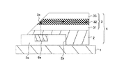
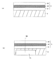
図1に示す光モジュールは、基板2と光導波路3とを有する光導波路基板4が配線基板1上に実装されており、さらに、光導波路基板4には、ヒートシンク5aに埋め込まれた光素子6aが直接接合されている。光導波路3は、クラッド部31,32に埋め込まれたコア部32を有し、当該光導波路3の端面が反射面となって光入出力部(光信号入出力部)3aを構成している。光入出力部3aは、例えば45°反射面から構成される。
【0021】
基板2は、使用する光に対して吸収のない光学的に透明な材料により形成されており、例えばガラス基板により構成されている。基板2の厚さは、例えば、200〜500μm程度である。なお、ガラス基板の他、Si基板、GaAs基板、サファイア基板により構成されていてもよい。
【0022】
上記の光導波路3が形成された基板2には、光素子6aと光導波路3の光信号入出力部3aとを低損失で光学的に結合させるため、ヒートシンク5aに埋め込まれた光素子6aの位置決めを行うための段差又は溝からなる位置決め部2aが設けられている。具体的には、位置決め部2aは、光素子6aの光軸中心が、光入出力部3aにおけるコア部32の光軸中心と合わさる位置に光素子6aを位置決めする。
【0023】
光導波路3を構成するコア部32は、使用する光に対して吸収がなく、かつクラッド部31,33よりも使用する光に対する屈折率が高い材料により形成されている。コア部32は、例えばエポキシ樹脂やフッ素化ポリイミド等の高分子材料により形成され、これらに不純物を加えることにより屈折率が調整される。
【0024】
クラッド部31,33は、使用する光に対して吸収がなく、かつコア部32よりも使用する光に対する屈折率が低い材料により形成されている。クラッド部31,33は、例えばエポキシ樹脂やフッ素化ポリイミド等の高分子材料により形成され、これらに不純物を加えることにより屈折率が調整される。なお、クラッド部31,33とコア部32とは、同種材料であっても、異種材料であってもよい。
【0025】
ヒートシンク5aは、熱伝達率の高い例えば金属材料により形成されており、光素子6aからの熱を外部に放出する。光素子6aが半導体レーザ等である場合、半導体レーザの発振波長の安定化を図るために設けられている。
【0026】
光素子6aは、フォトダイオート等の受光素子あるいはレーザダイオード等の発光素子により構成される。本実施形態では、光素子6aが発光素子の場合には、端面発光型半導体レーザではなく、面発光型半導体レーザ(面発光型発光素子)を用いる。
【0027】
なお、図示はしないが、光素子6aが埋め込まれたヒートシンク5aと基板2の位置決め部2aとの間、ヒートシンク5aと配線基板1との間、基板2と配線基板1との間には接着剤が塗布されており、当該接着剤により直接接合されている。特に、光素子6aが埋め込まれたヒートシンク5aと基板2の位置決め部2aとの間に塗布される接着剤は、光の散乱を防止する観点から、基板2の屈折率に近い接着剤を用いる。接着剤としては、例えば紫外線硬化樹脂を用いる。
また、光導波路3の先には、光ファイバが結合されていてもよく、あるいは他端側にも同様の反射面からなる光入出力部が形成されていてもよい。
【0028】
上記の本実施形態に係る光モジュールの動作について、図1を参照して説明する。
【0029】
光素子6aが面発光型発光素子である場合には、光素子6aから出射された送信用の信号光は基板2を透過して光導波路3の反射面からなる光入出力部3aに入射し、光入出力部3aにより反射されて光路が90°曲げられてコア部32に結合される。
コア部32に結合された光信号は、コア部32により導波されて、図示しない光導波路あるいは光ファイバにより導波され、図示しない受光素子により受光される。
【0030】
光素子6aが受光素子である場合には、光導波路3のコア部32を導波してきた受信用の信号光が、反射面からなる光入出力部3aに入射すると、当該光入出力部3aにより反射されて光路が90°曲げられて、受光素子からなる光素子6aに受光される。受光素子により光信号が電気信号に変換されて配線基板1上の図示しない受信回路に入力される。
【0031】
次に、上記の本実施形態に係る光導波路基板および光モジュールの製造方法について、図2〜図3を参照して説明する。
【0032】
まず、光導波路基板の製造方法について説明する。
基板2上にエポキシ樹脂あるいはフッ素化ポリイミド等を全面に塗布してクラッド部31を形成した後に、エポキシ樹脂あるいはフッ素化ポリイミド等をさらに全面に塗布してコア部32を形成する。クラッド部31とコア部32の屈折率差は、不純物を含有させて調整する。
【0033】
次に、コア部32上にフォトリソグラフィにより所望のパターンをもつレジストを形成し、当該レジストをマスクとしてコア部32の反応性イオンエッチングを行うことにより、コア部32のパターンを形成する。
【0034】
レジストを除去した後に、コア部32を覆うようにエポキシ樹脂あるいはフッ素化ポリイミド等を全面に塗布してクラッド部33を形成することにより、図2(a)に示すように基板2上に光導波路3が形成される。
【0035】
次に、図2(b)に示すように、ブレードソーによる機械的加工あるいはエッチングにより、基板2に段差又は溝からなる位置決め部2aを形成する。この位置決め部2aの形成において、光素子6aが埋め込まれたヒートシンク5aが位置決め部2aに嵌め込まれた際に、光入出力部のうちコア部32の中心部が、光素子6aの光軸中心に位置するように位置決め部32aを形成する。なお、図2(b)に示す加工面M1が、後に光入出力部となる。
【0036】
次に、図3(c)に示すように、ブレードソーによる機械的加工により例えば45°反射面となる光入出力部3aを形成する。機械的加工では、加工面M1の角度と等しい先端形状をもつブレードソーを用いればよい。なお、45°反射面をもつ光入出力部3aの形成は、エッチングにより行うことも可能である。
以上により、光入出力部3aおよび位置決め部2aを有する光導波路基板4が製造される。
【0037】
一方、図3(d)に示すように、光素子6aが埋め込まれたヒートシンク5aを配線基板1上に実装する。実装には、例えば紫外線硬化樹脂等からなる接着剤を用いる。
【0038】
そして、図3(c)に示す工程で製造された光導波路基板4の位置決め部2aを用いて、図3(d)に示す配線基板1上の光素子6aとの位置決め行い、光導波路基板4と光素子6aとを直接接合する。接合には、例えば紫外線硬化樹脂等からなる接着剤を用いる。
以上により、図1に示す本実施形態に係る光モジュールが製造される。
【0039】
本実施形態に係る光導波路基板4によれば、光導波路基板4に光素子6aを直接接合させる際に、基板2に光素子6aの位置決めを行う段差又は溝からなる位置決め部2aが設けられていることから、光導波路3と光素子6aとの位置を精度良く合わせることができる。
【0040】
従って、光導波路3と光素子6aとを結合させる際に、簡単なパッシブアライメントを用いても光導波路3と光素子6aとの結合効率を高めることができる。パッシブアライメントとは、光素子と光導波路を光軸合わせしてモジュール化する際に、光を用いずに目視や嵌め込み等による機械的な位置合わせのみで光軸合わせを行う方法をいう。これに対し、光を試験的に光路に入射させて光強度が最大となる箇所で光軸合わせ作業を行う方法をアクティブアライメントと呼ぶが、パッシブアライメントはアクティブアライメントに比べて、実装工程が簡素化されるため、光モジュールの低コスト化を図ることができる。
【0041】
また、上記の光導波路基板4を用いて光導波路3と光素子6aとが光学的に結合された光モジュールは、光導波路基板4に直接接合された光素子と光導波路との位置精度を向上することができ、光導波路と光素子との結合効率を高めることができる。
【0042】
第2実施形態
第1実施形態では、光素子6aが発光素子の場合には、面発光型発光素子を用いる場合の例について説明した。本実施形態では、発光素子として面発光型発光素子でなく、端面発光型発光素子を用いる場合における光導波路基板および光モジュールについて説明する。なお、第1実施形態と同一の構成要素には同一の符号を付しており、その説明は省略する。
【0043】
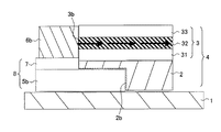
図4は、本実施形態に係る光導波路基板を備えた光モジュールの断面図である。
図4に示す光モジュールは、基板2と光導波路3とを有する光導波路基板4が配線基板1上に実装されており、さらに、光導波路基板4には、ヒートシンク5b上にサブマウント基板7を介して搭載された光素子6bが直接接合されている。上記のヒートシンク5bおよびサブマウント基板7が本発明の支持体8に相当する。
光導波路3は、クラッド部31,32に埋め込まれたコア部32を有し、当該光導波路3の端面は光軸に対して90°となる光入出力部(光信号入出力部)3bを構成している。
【0044】
本実施形態では、基板2を介して光信号の送受信を行わないため、使用する材料に特に限定はない。基板2の厚さは、例えば、200〜500μm程度である。基板2は、例えば、ガラス基板、Si基板、GaAs基板、あるいはサファイア基板により構成される。
【0045】
基板2には、光素子6bと光導波路3の光入出力部3bとを低損失で光学的に結合させるため、光素子6bを搭載する支持体8の位置決めを行うための段差又は溝からなる位置決め部2bが設けられている。具体的には、位置決め部2bは、光素子6bの光軸中心が、光入出力部3bにおけるコア部32の光軸中心と合わさる位置に光素子6bを位置決めする。
【0046】
光素子6bは、フォトダイオート等の受光素子あるいはレーザダイオード等の発光素子により構成される。本実施形態では、光素子6bが発光素子の場合には、面発光型半導体レーザではなく、端面発光型半導体レーザ(端面発光型発光素子)を用いる。
【0047】
なお、図示はしないが、光素子6bが搭載された支持体8と光導波路基板4との間、光導波路基板4と配線基板1との間には接着剤が塗布されており、当該接着剤により直接接合されている。特に、光素子6bが搭載された支持体8と基板2の位置決め部2bとの間に塗布される接着剤は、光の散乱を防止する観点から、コア部32の屈折率に近い接着剤を用いる。接着剤としては、例えば紫外線硬化樹脂を用いる。
また、光導波路3の先には、光ファイバが結合されていてもよく、あるいは他端側にも同様の光入出力部が形成されていてもよい。
【0048】
上記の本実施形態に係る光モジュールの動作について、図4を参照して説明する。
【0049】
光素子6bが端面発光型発光素子である場合には、光素子6bから出射された送信用の光信号は光導波路3の光入出力部3bに入射し、コア部32に結合される。
コア部32に結合された光信号は、コア部32により導波されて、図示しない光導波路あるいは光ファイバにより導波されて、図示しない受光素子により受光される。
【0050】
光素子6bが受光素子である場合には、光導波路3のコア部32を導波してきた受信用の光信号が、光入出力部3bに入射すると、当該光入出力部3bを介して光素子6bに受光される。受光素子により光信号が電気信号に変換されて配線基板1上の図示しない受信回路に入力される。
【0051】
次に、上記の本実施形態に係る光導波路および光モジュールの製造方法について、図5〜図6を参照して説明する。
【0052】
まず、図5(a)に示すように、第1実施形態と同様にして、基板2にクラッド部31,33およびコア部32を形成する。
【0053】
次に、図5(b)に示すように、ブレードソーによる機械的加工あるいはエッチングにより、基板2に段差又は溝からなる位置決め部2bを形成する。この位置決め部2bの形成において、位置決め部2bに支持体8が嵌め込まれた際に、光入出力部のうちコア部32の中心部が、光素子6bの光軸中心に位置するように位置決め部2bを形成する。なお、図5(b)に示す加工面M2が、後に入出力部となる。
【0054】
次に、図6(c)に示すように、ブレードソーによる機械的加工により例えば光導波路3の光軸に対して90°となる光入出力部3bを形成する。なお、光入出力部3bの形成は、エッチングにより行うことも可能である。
以上により、光入出力部3bおよび位置決め部2bを有する光導波路基板4が製造される。
【0055】
一方、図6(d)に示すように、例えばヒートシンク5bおよびサブマウント基板7からなる支持体8に支持された光素子6bを配線基板1上に実装する。実装には、例えば紫外線硬化樹脂等からなる接着剤を用いる。
【0056】
そして、図6(c)に示す工程で製造された光導波路基板4の位置決め部2bを用いて、図6(d)に示す配線基板1上の光素子6bとの位置決め行い、光導波路基板4と光素子6bとを直接接合する。接合には、例えば紫外線硬化樹脂等からなる接着剤を用いる。
以上により、図4に示す本実施形態に係る光モジュールが製造される。
【0057】
本実施形態に係る光導波路基板によれば、光導波路基板4に光素子6bを直接接合させる際に、基板2に光素子6bの位置決めを行う段差又は溝からなる位置決め部2bが設けられていることから、光導波路3と光素子6bとの位置を精度良く合わせることができる。
【0058】
従って、光導波路3と光素子6bとを結合させる際に、簡単なパッシブアライメントを用いても光導波路3と光素子6bとの結合効率を高めることができる。このように、実装工程が簡素化されるため、光モジュールの低コスト化を図ることができる。
【0059】
また、上記の光導波路基板4を用いて光導波路3と光素子6bとが光学的に結合された光モジュールは、光導波路基板4に直接接合された光素子と光導波路との位置精度を向上することができ、光導波路と光素子との結合効率を高めることができる。
【0060】
本発明の光導波路基板および光モジュールは、上記の実施形態の説明に限定されない。
例えば、基板2や、光導波路3を構成するクラッド部31,33およびコア部32を構成する材料には特に限定されず、また、ヒートシンク5a,5bは一例であり、基板2に位置決め部が設けられてあれば特に限定はない。また、第2実施形態におけるサブマウント基板7等は必要に応じて用いなくてもよい。
その他、本発明の要旨を逸脱しない範囲で、種々の変更が可能である。
【0061】
【発明の効果】
本発明の光導波路基板によれば、光導波路基板に光素子を直接接合させる際に、光導波路と光素子との位置を精度良く合わせることができる。
【0062】
本発明の光モジュールによれば、光導波路基板に光素子が直接接合され、かつ、光導波路と光素子との位置精度を向上することができることから、光導波路と光素子との結合効率を高めることができる。
【図面の簡単な説明】
【図1】第1実施形態に係る光導波路基板を備えた光モジュールの断面図である。
【図2】第1実施形態に係る光モジュールを製造するための工程断面図である。
【図3】図2の続きの工程を示す工程断面図である。
【図4】第2実施形態に係る光導波路基板を備えた光モジュールの断面図である。
【図5】第2実施形態に係る光モジュールを製造するための工程断面図である。
【図6】図5の続きの工程を示す工程断面図である。
【符号の説明】
1…配線基板、2…基板、2a,2b…位置決め部、3…光導波路、3a,3b…光入出力部、4…光導波路基板、5a,5b…ヒートシンク、6a,6b…光素子、7…サブマウント基板、8…支持体、31…クラッド部、32…コア部、33…クラッド部、M1,M2…加工面。[0001]
TECHNICAL FIELD OF THE INVENTION
The present invention relates to an optical waveguide substrate and an optical module, and more particularly to an optical waveguide substrate in which an optical waveguide is formed on a substrate and an optical element is optically coupled to the optical waveguide, and an optical element is optically coupled to the optical waveguide substrate. Optical module.
[0002]
[Prior art]
With the recent increase in circuit processing speed, signal delay and waveform distortion have occurred in electrical wiring, and accurate signal transmission has become impossible. In order to solve such a problem, attention has been paid to a conventional optical interconnection technique for transmitting a signal by replacing an electric signal with light. Replacing the electric signal with the optical signal can also solve the electromagnetic interference that has recently become a problem.
[0003]
From such a background, in recent years, in an optical communication system, an optical module in which an optical element such as a laser diode or a photodiode is coupled to an optical waveguide substrate having an optical waveguide formed on a substrate has been developed. In such an optical module, alignment between the optical waveguide provided on the substrate and the optical element is important in order to couple the optical waveguide and the optical element with low optical loss.
[0004]
As a conventional optical module, there is a module that optically couples a surface emitting light emitting device and an optical waveguide by physically directly bonding an end of a flexible optical waveguide to the surface emitting light emitting device (Patent) Reference 1).
[0005]
As another optical module, there is an optical module which is coupled to a film-shaped optical waveguide using a bump made of solder or the like (see Patent Document 2).
[0006]
[Patent Document 1]
JP 2001-188146 A [Patent Document 2]
Patent No. 3257776 [0007]
[Problems to be solved by the invention]
However, in the optical module described in Patent Literature 1, it is difficult to accurately perform positioning and bonding at the time of bonding because an optical waveguide coupled to an optical element such as a surface-emitting type light emitting element is flexible. In addition, a connection groove for optically coupling the optical waveguide provided on the substrate side to the flexible optical waveguide is provided on the substrate. In this case, too, the optical waveguide is flexible, so Is a problem.
[0008]
Further, when an optical waveguide and an optical element are coupled by using a bump such as solder as in the optical module described in
[0009]
The present invention has been made in view of the above circumstances, and an object of the present invention is to provide an optical waveguide substrate capable of accurately aligning an optical waveguide and an optical element when an optical element is directly bonded to the optical waveguide substrate. Is to provide.
Another object of the present invention is to improve the positional accuracy between an optical device directly bonded to an optical waveguide substrate and the optical waveguide, thereby improving the coupling efficiency between the optical waveguide and the optical device. Is to provide.
[0010]
[Means for Solving the Problems]
In order to achieve the above object, an optical waveguide substrate of the present invention is an optical waveguide substrate in which an optical waveguide is formed on a substrate and an optical element is optically coupled to an optical signal input / output unit of the optical waveguide. A positioning portion for optically coupling the optical element to the optical signal input / output portion of the optical waveguide is formed on the substrate.
[0011]
The optical signal input / output unit reflects an incident optical signal to optically couple the optical element and the optical waveguide, and the positioning unit connects the substrate by directly joining the optical element to the substrate. The optical element is positioned so as to be optically coupled to the optical signal input / output unit through the optical element.
[0012]
The positioning section positions the optical element such that the optical element is directly joined to the optical signal input / output section of the optical waveguide and optically coupled to the optical signal input / output section.
[0013]
According to the above-described optical waveguide substrate of the present invention, since the positioning portion is formed on the substrate on which the optical waveguide is formed, the position of the optical element and the optical signal input / output portion of the optical waveguide is determined using the positioning portion. By performing the alignment, the optical element is optically coupled to the optical signal input / output unit of the optical waveguide.
[0014]
Further, in order to achieve the above object, an optical module according to the present invention has an optical waveguide substrate having an optical waveguide formed on a substrate, and an optical element is optically coupled to an optical signal input / output unit of the optical waveguide. A positioning unit for optically coupling the optical element to the optical signal input / output unit of the optical waveguide is formed on the substrate.
[0015]
The optical signal input / output unit reflects an incident optical signal to optically couple the optical element and the optical waveguide, and the positioning unit connects the substrate by directly joining the optical element to the substrate. The optical element is positioned so as to be optically coupled to the optical signal input / output unit through the optical element. The optical element is a surface emitting light emitting element.
[0016]
The positioning section positions the optical element such that the optical element is directly joined to the optical signal input / output section of the optical waveguide and optically coupled to the optical signal input / output section. The optical element is an edge emitting light emitting element.
[0017]
The edge-emitting light-emitting element is supported by a support, and the positioning portion is configured such that the edge-emitting light-emitting element is directly joined to the optical signal input / output section of the optical waveguide and is connected to the optical signal input / output section. The support and the edge-emitting light emitting device are positioned so as to be optically coupled.
[0018]
According to the optical module of the present invention, since the positioning portion is formed on the substrate on which the optical waveguide is formed, the positioning between the optical element and the optical signal input / output portion of the optical waveguide is performed using the positioning portion. Is performed, and the optical element is optically coupled to the optical signal input / output unit of the optical waveguide.
[0019]
BEST MODE FOR CARRYING OUT THE INVENTION
Hereinafter, embodiments of an optical waveguide substrate and an optical module according to the present invention will be described with reference to the drawings.
[0020]
First Embodiment FIG. 1 is a sectional view of an optical module including an optical waveguide substrate according to the present embodiment.
In the optical module shown in FIG. 1, an
[0021]
The
[0022]
In order to optically couple the
[0023]
The
[0024]
The
[0025]
The
[0026]
The
[0027]
Although not shown, an adhesive is provided between the
In addition, an optical fiber may be coupled to the end of the
[0028]
The operation of the optical module according to the embodiment will be described with reference to FIG.
[0029]
When the
The optical signal coupled to the
[0030]
When the
[0031]
Next, a method for manufacturing the optical waveguide substrate and the optical module according to the present embodiment will be described with reference to FIGS.
[0032]
First, a method for manufacturing an optical waveguide substrate will be described.
After a
[0033]
Next, a resist having a desired pattern is formed on the
[0034]
After the resist is removed, an epoxy resin or fluorinated polyimide or the like is applied on the entire surface so as to cover the
[0035]
Next, as shown in FIG. 2B, a
[0036]
Next, as shown in FIG. 3C, an optical input /
As described above, the
[0037]
On the other hand, as shown in FIG. 3D, the
[0038]
Then, by using the
As described above, the optical module according to the present embodiment shown in FIG. 1 is manufactured.
[0039]
According to the
[0040]
Therefore, when coupling the
[0041]
Further, the optical module in which the
[0042]
Second Embodiment In the first embodiment, an example has been described in which the surface emitting light emitting element is used when the
[0043]
FIG. 4 is a cross-sectional view of an optical module including the optical waveguide substrate according to the present embodiment.
In the optical module shown in FIG. 4, an
The
[0044]
In the present embodiment, the transmission and reception of the optical signal via the
[0045]
In order to optically couple the
[0046]
The
[0047]
Although not shown, an adhesive is applied between the
Further, an optical fiber may be coupled to the end of the
[0048]
The operation of the optical module according to the embodiment will be described with reference to FIG.
[0049]
When the
The optical signal coupled to the
[0050]
When the
[0051]
Next, a method for manufacturing the optical waveguide and the optical module according to the above-described embodiment will be described with reference to FIGS.
[0052]
First, as shown in FIG. 5A, clad
[0053]
Next, as shown in FIG. 5B, a
[0054]
Next, as shown in FIG. 6C, an optical input /
As described above, the
[0055]
On the other hand, as shown in FIG. 6D, for example, the
[0056]
Then, by using the
Thus, the optical module according to the present embodiment shown in FIG. 4 is manufactured.
[0057]
According to the optical waveguide substrate according to the present embodiment, when the
[0058]
Therefore, when coupling the
[0059]
Further, the optical module in which the
[0060]
The optical waveguide substrate and the optical module of the present invention are not limited to the description of the above embodiment.
For example, the material forming the
In addition, various changes can be made without departing from the spirit of the present invention.
[0061]
【The invention's effect】
According to the optical waveguide substrate of the present invention, when the optical element is directly joined to the optical waveguide substrate, the positions of the optical waveguide and the optical element can be accurately adjusted.
[0062]
According to the optical module of the present invention, since the optical element is directly bonded to the optical waveguide substrate and the positional accuracy between the optical waveguide and the optical element can be improved, the coupling efficiency between the optical waveguide and the optical element is increased. be able to.
[Brief description of the drawings]
FIG. 1 is a cross-sectional view of an optical module including an optical waveguide substrate according to a first embodiment.
FIG. 2 is a process sectional view for manufacturing the optical module according to the first embodiment.
FIG. 3 is a process sectional view showing a process continued from FIG. 2;
FIG. 4 is a cross-sectional view of an optical module including an optical waveguide substrate according to a second embodiment.
FIG. 5 is a process sectional view for manufacturing the optical module according to the second embodiment.
FIG. 6 is a process cross-sectional view showing a process continued from FIG. 5;
[Explanation of symbols]
DESCRIPTION OF SYMBOLS 1 ... Wiring board, 2 ... Substrate, 2a, 2b ... Positioning part, 3 ... Optical waveguide, 3a, 3b ... Optical input / output part, 4 ... Optical waveguide board, 5a, 5b ... Heat sink, 6a, 6b ... Optical element, 7 ... submount substrate, 8 ... support, 31 ... cladding part, 32 ... core part, 33 ... cladding part, M1, M2 ... work surface.
Claims (9)
前記光素子を前記光導波路の前記光信号入出力部に光学的に結合させる位置決め部が前記基板に形成されている
光導波路基板。An optical waveguide substrate in which an optical waveguide is formed on the substrate and an optical element is optically coupled to an optical signal input / output unit of the optical waveguide,
An optical waveguide substrate, wherein a positioning portion for optically coupling the optical element to the optical signal input / output portion of the optical waveguide is formed on the substrate.
前記位置決め部は、前記光素子が前記基板に直接接合されて前記基板を介して前記光信号入出力部に光学的に結合されるように、前記光素子を位置決めする
請求項1記載の光導波路基板。The optical signal input / output unit optically couples the optical element and the optical waveguide by reflecting an incident optical signal,
The optical waveguide according to claim 1, wherein the positioning unit positions the optical element such that the optical element is directly bonded to the substrate and optically coupled to the optical signal input / output unit via the substrate. substrate.
請求項1記載の光導波路基板。2. The positioning section positions the optical element such that the optical element is directly joined to the optical signal input / output section of the optical waveguide and optically coupled to the optical signal input / output section. 3. Optical waveguide substrate.
前記光素子を前記光導波路の前記光信号入出力部に光学的に結合させる位置決め部が前記基板に形成されている
光モジュール。An optical module having an optical waveguide substrate having an optical waveguide formed on a substrate, and an optical element optically coupled to an optical signal input / output unit of the optical waveguide,
An optical module, wherein a positioning portion for optically coupling the optical element to the optical signal input / output portion of the optical waveguide is formed on the substrate.
前記位置決め部は、前記光素子が前記基板に直接接合されて前記基板を介して前記光信号入出力部に光学的に結合されるように、前記光素子を位置決めする
請求項4記載の光モジュール。The optical signal input / output unit optically couples the optical element and the optical waveguide by reflecting an incident optical signal,
The optical module according to claim 4, wherein the positioning unit positions the optical element such that the optical element is directly bonded to the substrate and optically coupled to the optical signal input / output unit via the substrate. .
請求項5記載の光モジュール。The optical module according to claim 5, wherein the optical element is a surface-emitting type light emitting element.
請求項4記載の光モジュール。5. The positioning unit according to claim 4, wherein the positioning unit positions the optical element such that the optical element is directly joined to the optical signal input / output unit of the optical waveguide and optically coupled to the optical signal input / output unit. Optical module.
請求項7記載の光モジュール。The optical module according to claim 7, wherein the optical element is an edge-emitting light emitting element.
前記位置決め部は、前記端面発光型発光素子が前記光導波路の前記光信号入出力部に直接接合されて前記光信号入出力部に光学的に結合されるように、前記支持体および前記端面発光型発光素子を位置決めする
請求項8記載の光モジュール。The edge-emitting light emitting element is supported by a support,
The support and the edge light-emitting device are arranged such that the edge-emitting type light emitting element is directly joined to the optical signal input / output portion of the optical waveguide and optically coupled to the optical signal input / output portion. 9. The optical module according to claim 8, wherein the light emitting element is positioned.
Priority Applications (1)
| Application Number | Priority Date | Filing Date | Title |
|---|---|---|---|
| JP2003022612A JP2004233687A (en) | 2003-01-30 | 2003-01-30 | Optical waveguide substrate and optical module |
Applications Claiming Priority (1)
| Application Number | Priority Date | Filing Date | Title |
|---|---|---|---|
| JP2003022612A JP2004233687A (en) | 2003-01-30 | 2003-01-30 | Optical waveguide substrate and optical module |
Publications (1)
| Publication Number | Publication Date |
|---|---|
| JP2004233687A true JP2004233687A (en) | 2004-08-19 |
Family
ID=32951640
Family Applications (1)
| Application Number | Title | Priority Date | Filing Date |
|---|---|---|---|
| JP2003022612A Pending JP2004233687A (en) | 2003-01-30 | 2003-01-30 | Optical waveguide substrate and optical module |
Country Status (1)
| Country | Link |
|---|---|
| JP (1) | JP2004233687A (en) |
Cited By (10)
| Publication number | Priority date | Publication date | Assignee | Title |
|---|---|---|---|---|
| JP2007148107A (en) * | 2005-11-29 | 2007-06-14 | Omron Corp | Optical cable module, its manufacturing method and electronic equipment having the same |
| JP2008152060A (en) * | 2006-12-19 | 2008-07-03 | Fujikura Ltd | Optical path conversion-type optical connector and circuit board using the same |
| JP2008176071A (en) * | 2007-01-18 | 2008-07-31 | Omron Corp | Optical transmission module, electronic device, and manufacturing method for the optical transmission module |
| JPWO2007074911A1 (en) * | 2005-12-28 | 2009-06-04 | オムロン株式会社 | Optical module |
| JP2009198804A (en) * | 2008-02-21 | 2009-09-03 | Sony Corp | Optical module and optical waveguide |
| US7590315B2 (en) * | 2006-12-08 | 2009-09-15 | Sony Corporation | Optical waveguide and optical module using the same |
| US7657140B2 (en) | 2006-04-07 | 2010-02-02 | Omron Corporation | Optical cable module |
| JP2010152075A (en) * | 2008-12-25 | 2010-07-08 | Fuji Xerox Co Ltd | Optical transmission apparatus |
| JP2012150242A (en) * | 2011-01-18 | 2012-08-09 | Hitachi Chem Co Ltd | Method of manufacturing optical waveguide with mirror, optical waveguide with mirror, and opto-electric composite substrate with mirror |
| JP5321740B2 (en) * | 2010-05-12 | 2013-10-23 | コニカミノルタ株式会社 | Scanning optical system and projector provided with the same |
-
2003
- 2003-01-30 JP JP2003022612A patent/JP2004233687A/en active Pending
Cited By (13)
| Publication number | Priority date | Publication date | Assignee | Title |
|---|---|---|---|---|
| JP4631671B2 (en) * | 2005-11-29 | 2011-02-16 | オムロン株式会社 | Optical cable module and electronic device including optical cable module |
| JP2007148107A (en) * | 2005-11-29 | 2007-06-14 | Omron Corp | Optical cable module, its manufacturing method and electronic equipment having the same |
| JP4645651B2 (en) * | 2005-12-28 | 2011-03-09 | オムロン株式会社 | Optical module |
| JPWO2007074911A1 (en) * | 2005-12-28 | 2009-06-04 | オムロン株式会社 | Optical module |
| US7657140B2 (en) | 2006-04-07 | 2010-02-02 | Omron Corporation | Optical cable module |
| US7590315B2 (en) * | 2006-12-08 | 2009-09-15 | Sony Corporation | Optical waveguide and optical module using the same |
| JP2008152060A (en) * | 2006-12-19 | 2008-07-03 | Fujikura Ltd | Optical path conversion-type optical connector and circuit board using the same |
| JP2008176071A (en) * | 2007-01-18 | 2008-07-31 | Omron Corp | Optical transmission module, electronic device, and manufacturing method for the optical transmission module |
| JP2009198804A (en) * | 2008-02-21 | 2009-09-03 | Sony Corp | Optical module and optical waveguide |
| US8100589B2 (en) | 2008-02-21 | 2012-01-24 | Sony Corporation | Optical module and optical waveguide |
| JP2010152075A (en) * | 2008-12-25 | 2010-07-08 | Fuji Xerox Co Ltd | Optical transmission apparatus |
| JP5321740B2 (en) * | 2010-05-12 | 2013-10-23 | コニカミノルタ株式会社 | Scanning optical system and projector provided with the same |
| JP2012150242A (en) * | 2011-01-18 | 2012-08-09 | Hitachi Chem Co Ltd | Method of manufacturing optical waveguide with mirror, optical waveguide with mirror, and opto-electric composite substrate with mirror |
Similar Documents
| Publication | Publication Date | Title |
|---|---|---|
| US8827572B2 (en) | Side coupling optical fiber assembly and fabrication method thereof | |
| US6912332B2 (en) | Parallel optical interconnection module and method for manufacturing the same | |
| JP7117133B2 (en) | Optical subassembly, manufacturing method thereof, and optical module | |
| KR19980030121A (en) | Optical module with lens aligned in V-groove and manufacturing method thereof | |
| TW442678B (en) | Connector-type optical transceiver using SOI optical waveguide | |
| JP2004029798A (en) | Alignment device | |
| JP2014522999A (en) | Optical interposer with common inclined surface | |
| JP2002033546A (en) | Surface emitting optical element, surface emitting optical element mount, its manufacturing method and optical wiring device using the same | |
| JP2004233687A (en) | Optical waveguide substrate and optical module | |
| JP2006267502A (en) | Optical waveguide module | |
| JP2008102283A (en) | Optical waveguide, optical module and method of manufacturing optical waveguide | |
| JP6929103B2 (en) | Optical module | |
| JP2009008766A (en) | Optical module | |
| JPH10170765A (en) | Optical waveguide | |
| JP2007086367A (en) | Optical pin, optical pin connector and optical path conversion module | |
| JP2006201499A (en) | Optical communication module | |
| JP3835018B2 (en) | Optical device including optical device and optical device | |
| JP2004251976A (en) | Optical module | |
| JP4288604B2 (en) | Optical coupling device | |
| JP2001188146A (en) | Optical coupling method and optical circuit | |
| JP2005070141A (en) | Optical waveguide structure with optical path conversion component and manufacturing method therefor and optical path conversion component | |
| JP2006030224A (en) | Optical waveguide and optical coupling device | |
| JP2009008767A (en) | Optical module | |
| JP4119809B2 (en) | Opto-electric hybrid board | |
| JP2000321453A (en) | Optical switching device and optical transmitter and manufacture of these |