JP2004207696A - Aligner and method for manufacturing device - Google Patents
Aligner and method for manufacturing device Download PDFInfo
- Publication number
- JP2004207696A JP2004207696A JP2003393858A JP2003393858A JP2004207696A JP 2004207696 A JP2004207696 A JP 2004207696A JP 2003393858 A JP2003393858 A JP 2003393858A JP 2003393858 A JP2003393858 A JP 2003393858A JP 2004207696 A JP2004207696 A JP 2004207696A
- Authority
- JP
- Japan
- Prior art keywords
- substrate
- liquid
- light
- exposure
- exposure apparatus
- Prior art date
- Legal status (The legal status is an assumption and is not a legal conclusion. Google has not performed a legal analysis and makes no representation as to the accuracy of the status listed.)
- Granted
Links
- 238000004519 manufacturing process Methods 0.000 title claims description 16
- 238000000034 method Methods 0.000 title description 31
- 239000007788 liquid Substances 0.000 claims abstract description 324
- 239000000758 substrate Substances 0.000 claims abstract description 291
- 230000003287 optical effect Effects 0.000 claims abstract description 279
- 238000001514 detection method Methods 0.000 claims description 235
- 230000001678 irradiating effect Effects 0.000 claims description 5
- 230000006866 deterioration Effects 0.000 abstract description 2
- 238000007654 immersion Methods 0.000 description 70
- 238000011084 recovery Methods 0.000 description 45
- 238000012545 processing Methods 0.000 description 40
- 238000005259 measurement Methods 0.000 description 17
- 238000010586 diagram Methods 0.000 description 15
- XLYOFNOQVPJJNP-UHFFFAOYSA-N water Substances O XLYOFNOQVPJJNP-UHFFFAOYSA-N 0.000 description 13
- 230000008569 process Effects 0.000 description 12
- 238000003860 storage Methods 0.000 description 12
- 239000003795 chemical substances by application Substances 0.000 description 9
- 230000002950 deficient Effects 0.000 description 9
- 239000004065 semiconductor Substances 0.000 description 9
- 230000007423 decrease Effects 0.000 description 8
- 238000005286 illumination Methods 0.000 description 7
- 238000012546 transfer Methods 0.000 description 6
- 230000015572 biosynthetic process Effects 0.000 description 4
- 230000007547 defect Effects 0.000 description 4
- 101000891579 Homo sapiens Microtubule-associated protein tau Proteins 0.000 description 3
- 102100040243 Microtubule-associated protein tau Human genes 0.000 description 3
- 239000008186 active pharmaceutical agent Substances 0.000 description 3
- 238000013461 design Methods 0.000 description 3
- 238000009434 installation Methods 0.000 description 3
- XUIMIQQOPSSXEZ-UHFFFAOYSA-N Silicon Chemical compound [Si] XUIMIQQOPSSXEZ-UHFFFAOYSA-N 0.000 description 2
- 230000004075 alteration Effects 0.000 description 2
- 230000008901 benefit Effects 0.000 description 2
- 238000009826 distribution Methods 0.000 description 2
- 230000000694 effects Effects 0.000 description 2
- 239000012535 impurity Substances 0.000 description 2
- 238000005339 levitation Methods 0.000 description 2
- 239000004973 liquid crystal related substance Substances 0.000 description 2
- QSHDDOUJBYECFT-UHFFFAOYSA-N mercury Chemical compound [Hg] QSHDDOUJBYECFT-UHFFFAOYSA-N 0.000 description 2
- 229910052753 mercury Inorganic materials 0.000 description 2
- 229910052751 metal Inorganic materials 0.000 description 2
- 239000002184 metal Substances 0.000 description 2
- 231100000989 no adverse effect Toxicity 0.000 description 2
- 239000003921 oil Substances 0.000 description 2
- 238000000206 photolithography Methods 0.000 description 2
- 229920002120 photoresistant polymer Polymers 0.000 description 2
- 238000004904 shortening Methods 0.000 description 2
- 229910052710 silicon Inorganic materials 0.000 description 2
- 239000010703 silicon Substances 0.000 description 2
- 239000000126 substance Substances 0.000 description 2
- 239000010409 thin film Substances 0.000 description 2
- 241000218645 Cedrus Species 0.000 description 1
- 206010010071 Coma Diseases 0.000 description 1
- YCKRFDGAMUMZLT-UHFFFAOYSA-N Fluorine atom Chemical compound [F] YCKRFDGAMUMZLT-UHFFFAOYSA-N 0.000 description 1
- 239000004721 Polyphenylene oxide Substances 0.000 description 1
- 239000000919 ceramic Substances 0.000 description 1
- 238000004140 cleaning Methods 0.000 description 1
- 230000003749 cleanliness Effects 0.000 description 1
- 230000007797 corrosion Effects 0.000 description 1
- 238000005260 corrosion Methods 0.000 description 1
- 239000006059 cover glass Substances 0.000 description 1
- 230000003247 decreasing effect Effects 0.000 description 1
- 229910052731 fluorine Inorganic materials 0.000 description 1
- 239000011737 fluorine Substances 0.000 description 1
- 230000014509 gene expression Effects 0.000 description 1
- 239000011521 glass Substances 0.000 description 1
- 238000003384 imaging method Methods 0.000 description 1
- 230000006872 improvement Effects 0.000 description 1
- 238000007689 inspection Methods 0.000 description 1
- 230000010354 integration Effects 0.000 description 1
- 238000012423 maintenance Methods 0.000 description 1
- 230000007257 malfunction Effects 0.000 description 1
- 239000000463 material Substances 0.000 description 1
- 239000011159 matrix material Substances 0.000 description 1
- 230000007246 mechanism Effects 0.000 description 1
- 239000003960 organic solvent Substances 0.000 description 1
- 238000004806 packaging method and process Methods 0.000 description 1
- 239000002245 particle Substances 0.000 description 1
- 229920000570 polyether Polymers 0.000 description 1
- 239000010453 quartz Substances 0.000 description 1
- 230000009467 reduction Effects 0.000 description 1
- 238000000926 separation method Methods 0.000 description 1
- VYPSYNLAJGMNEJ-UHFFFAOYSA-N silicon dioxide Inorganic materials O=[Si]=O VYPSYNLAJGMNEJ-UHFFFAOYSA-N 0.000 description 1
- 230000001360 synchronised effect Effects 0.000 description 1
- 238000002834 transmittance Methods 0.000 description 1
Images


Classifications
-
- G—PHYSICS
- G03—PHOTOGRAPHY; CINEMATOGRAPHY; ANALOGOUS TECHNIQUES USING WAVES OTHER THAN OPTICAL WAVES; ELECTROGRAPHY; HOLOGRAPHY
- G03F—PHOTOMECHANICAL PRODUCTION OF TEXTURED OR PATTERNED SURFACES, e.g. FOR PRINTING, FOR PROCESSING OF SEMICONDUCTOR DEVICES; MATERIALS THEREFOR; ORIGINALS THEREFOR; APPARATUS SPECIALLY ADAPTED THEREFOR
- G03F7/00—Photomechanical, e.g. photolithographic, production of textured or patterned surfaces, e.g. printing surfaces; Materials therefor, e.g. comprising photoresists; Apparatus specially adapted therefor
- G03F7/70—Microphotolithographic exposure; Apparatus therefor
- G03F7/70216—Mask projection systems
- G03F7/70341—Details of immersion lithography aspects, e.g. exposure media or control of immersion liquid supply
Landscapes
- Physics & Mathematics (AREA)
- General Physics & Mathematics (AREA)
- Exposure And Positioning Against Photoresist Photosensitive Materials (AREA)
- Exposure Of Semiconductors, Excluding Electron Or Ion Beam Exposure (AREA)
- Investigating Materials By The Use Of Optical Means Adapted For Particular Applications (AREA)
- Investigating Or Analysing Materials By Optical Means (AREA)
Abstract
Description
本発明は、投影光学系と基板との間の少なくとも一部を液体で満たした状態で投影光学系を介して基板にパターンを露光する露光装置、及びこの露光装置を用いるデバイス製造方法に関するものである。 The present invention relates to an exposure apparatus that exposes a substrate to a pattern via a projection optical system while at least a portion between the projection optical system and the substrate is filled with a liquid, and a device manufacturing method using the exposure apparatus. is there.
半導体デバイスや液晶表示デバイスは、マスク上に形成されたパターンを感光性の基板上に転写する、いわゆるフォトリソグラフィの手法により製造される。このフォトリソグラフィ工程で使用される露光装置は、マスクを支持するマスクステージと基板を支持する基板ステージとを有し、マスクステージ及び基板ステージを逐次移動しながらマスクのパターンを投影光学系を介して基板に転写するものである。近年、デバイスパターンのより一層の高集積化に対応するために投影光学系の更なる高解像度化が望まれている。投影光学系の解像度は、使用する露光波長が短くなるほど、また投影光学系の開口数が大きいほど高くなる。そのため、露光装置で使用される露光波長は年々短波長化しており、投影光学系の開口数も増大している。そして、現在主流の露光波長は、KrFエキシマレーザの248nmであるが、更に短波長のArFエキシマレーザの193nmも実用化されつつある。また、露光を行う際には、解像度と同様に焦点深度(DOF)も重要となる。解像度R、及び焦点深度δはそれぞれ以下の式で表される。
R=k1・λ/NA … (1)
δ=±k2・λ/NA2 … (2)
ここで、λは露光波長、NAは投影光学系の開口数、k1、k2はプロセス係数である。(1)式、(2)式より、解像度Rを高めるために、露光波長λを短くして、開口数NAを大きくすると、焦点深度δが狭くなることが分かる。
A semiconductor device and a liquid crystal display device are manufactured by a so-called photolithography technique of transferring a pattern formed on a mask onto a photosensitive substrate. The exposure apparatus used in this photolithography process has a mask stage that supports a mask and a substrate stage that supports a substrate, and sequentially moves the mask stage and the substrate stage to project a pattern of the mask through a projection optical system. This is to be transferred to a substrate. In recent years, further improvement in the resolution of the projection optical system has been desired in order to cope with higher integration of device patterns. The resolution of the projection optical system increases as the exposure wavelength used decreases and as the numerical aperture of the projection optical system increases. For this reason, the exposure wavelength used in the exposure apparatus is becoming shorter year by year, and the numerical aperture of the projection optical system is also increasing. The exposure wavelength currently mainstream is 248 nm of KrF excimer laser, but 193 nm of shorter wavelength ArF excimer laser is also being put to practical use. When performing exposure, the depth of focus (DOF) becomes important as well as the resolution. The resolution R and the depth of focus δ are respectively represented by the following equations.
R = k 1 · λ / NA (1)
δ = ± k 2 · λ / NA 2 (2)
Here, λ is the exposure wavelength, NA is the numerical aperture of the projection optical system, and k 1 and k 2 are the process coefficients. From the expressions (1) and (2), it can be seen that when the exposure wavelength λ is shortened and the numerical aperture NA is increased in order to increase the resolution R, the depth of focus δ becomes narrower.
焦点深度δが狭くなり過ぎると、投影光学系の像面に対して基板表面を合致させることが困難となり、露光動作時のマージンが不足する恐れがある。そこで、実質的に露光波長を短くして、且つ焦点深度を広くする方法として、例えば下記特許文献1に開示されている液浸法が提案されている。この液浸法は、投影光学系の下面と基板表面との間を水や有機溶媒等の液体で満たし、液体中での露光光の波長が、空気中の1/n(nは液体の屈折率で通常1.2〜1.6程度)になることを利用して解像度を向上するとともに、焦点深度を約n倍に拡大するというものである。
液浸法により露光処理を行う場合、投影光学系と基板との間の液体中(特に、基板の表面)に気泡などの気体部分が存在すると、この気泡(気体部分)により基板上に形成されるパターン像が劣化する恐れがある。例えば、気泡は、供給されている液体に含まれている場合だけでなく、その供給後に液体中で発生する可能性もある。そのようなパターンの像の結像不良を放置しておくと、最終的なデバイスになってから不良品として発見することになり、デバイス生産性の低下を招く恐れがある。 In the case of performing the exposure processing by the immersion method, if a gas portion such as bubbles is present in the liquid between the projection optical system and the substrate (particularly, the surface of the substrate), the gas is formed on the substrate by the bubbles (gas portion). Pattern image may be degraded. For example, bubbles may be generated in the liquid after the supply, as well as when contained in the supplied liquid. If the image formation failure of such an image of the pattern is left unchecked, it will be discovered as a defective product after the final device is formed, which may lead to a decrease in device productivity.
また、液浸法に基づく露光処理を行う際、投影光学系と基板との間に液体を供給する液体供給装置が動作不能となる等、なんらかの原因で投影光学系と基板との間の少なくとも一部に液体が満たされない状態が生じて気体部分が形成される場合が考えられる。すなわち、パターンの像のすべて、あるいは一部が液体を介さずに基板上に投影されてしまう恐れがある。この場合、パターンの像が基板上で結像しない可能性があり、放置しておくと、最終的なデバイスになるまで不良であることが発見できず、生産性の低下を招く恐れがある。 In addition, when performing the exposure process based on the liquid immersion method, at least one of the distances between the projection optical system and the substrate for some reason such as a liquid supply device that supplies liquid between the projection optical system and the substrate becomes inoperable. It is conceivable that a state in which the liquid is not filled in the portion occurs and a gas portion is formed. That is, all or a part of the image of the pattern may be projected onto the substrate without passing through the liquid. In this case, the image of the pattern may not be formed on the substrate, and if left unchecked, a defect cannot be found until a final device is formed, which may lead to a decrease in productivity.
また、液浸法を用いる場合には、投影光学系の像面側の液体を介して各種の計測を行う場合があるが、投影光学系の像面側に気体部分が存在し、十分に液体で満たされていないと、計測誤差が発生したり、計測不能状態に陥る可能性もある。 When using the liquid immersion method, various measurements may be performed via the liquid on the image plane side of the projection optical system. If not, there is a possibility that a measurement error may occur or the measurement may not be possible.
本発明はこのような事情に鑑みてなされたものであって、液浸法を用いる場合にも、生産性の低下を抑えることができる露光装置、及びこの露光装置を用いるデバイス製造方法を提供することを目的とする。また、投影光学系と基板との間に液体を満たして露光処理する際、液体中の気泡に起因するパターン像の劣化などを検知できる露光装置、及びこの露光装置を用いるデバイス製造方法を提供することを目的とする。また、投影光学系と基板との間に液体が満たされないことに起因する生産性の低下を抑えることができる露光装置、及びこの露光装置を用いるデバイス製造方法を提供することを目的とする。また、本発明は、液浸法を用いる場合にも、露光不良や計測不良などの発生を抑えることのできる露光装置、及びこの露光装置を用いるデバイス製造方法を提供することを目的とする。 The present invention has been made in view of such circumstances, and provides an exposure apparatus capable of suppressing a decrease in productivity even when using an immersion method, and a device manufacturing method using the exposure apparatus. The purpose is to: Further, there is provided an exposure apparatus capable of detecting deterioration of a pattern image or the like caused by bubbles in a liquid when a liquid is filled between a projection optical system and a substrate, and a device manufacturing method using the exposure apparatus. The purpose is to: It is another object of the present invention to provide an exposure apparatus capable of suppressing a decrease in productivity caused by a liquid being not filled between a projection optical system and a substrate, and a device manufacturing method using the exposure apparatus. Another object of the present invention is to provide an exposure apparatus capable of suppressing the occurrence of exposure failure and measurement failure even when using the liquid immersion method, and a device manufacturing method using the exposure apparatus.
上記の課題を解決するため、本発明は実施の形態に示す図1〜図16に対応付けした以下の構成を採用している。
本発明の露光装置(EX)は、投影光学系(PL)と基板(P)との間の少なくとも一部を液体(50)で満たし、投影光学系(PL)と液体(50)とを介してパターンの像を基板(P)上に投影することによって、基板(P)を露光する露光装置において、投影光学系(PL)と基板(P)との間の液体(50)中の気泡を検出する気泡検出器(20)を備えたことを特徴とする。
また、本発明のデバイス製造方法は、上記記載の露光装置(EX)を用いることを特徴とする。
In order to solve the above-described problem, the present invention employs the following configuration corresponding to FIGS.
The exposure apparatus (EX) of the present invention fills at least a part between the projection optical system (PL) and the substrate (P) with the liquid (50), and interposes the liquid through the projection optical system (PL) and the liquid (50). In an exposure apparatus that exposes the substrate (P) by projecting an image of the pattern onto the substrate (P), bubbles in the liquid (50) between the projection optical system (PL) and the substrate (P) are removed. A bubble detector (20) for detection is provided.
Further, a device manufacturing method of the present invention uses the above-described exposure apparatus (EX).
本発明によれば、液浸法に基づいて露光処理する際、気泡検出器により投影光学系と基板との間の液体中の気泡を検出することで、パターン転写精度に大きく係わる部分である投影光学系と基板との間の液体中の気泡に関する情報を検出することができる。したがって、この検出結果に基づいて露光不良(不良ショット)を把握できるため、高いデバイス生産性を維持するための適切な処置を施すことができる。 According to the present invention, when performing exposure processing based on the liquid immersion method, by detecting bubbles in the liquid between the projection optical system and the substrate with the bubble detector, the projection which is a part greatly related to the pattern transfer accuracy is performed. Information about bubbles in the liquid between the optical system and the substrate can be detected. Therefore, an exposure defect (defective shot) can be grasped on the basis of the detection result, so that an appropriate measure for maintaining high device productivity can be taken.
本発明の露光装置(EX)は、投影光学系(PL)と基板(P)との間の少なくとも一部を液体(50)で満たし、投影光学系(PL)と液体(50)とを介してパターンの像を基板(P)上に投影することによって、基板(P)を露光する露光装置において、投影光学系(PL)と基板(P)との間の少なくとも一部の液体(50)が切れるのを検出する液切検出装置(20)を備えることを特徴とする。 The exposure apparatus (EX) of the present invention fills at least a part between the projection optical system (PL) and the substrate (P) with the liquid (50), and interposes the liquid through the projection optical system (PL) and the liquid (50). In an exposure apparatus for exposing the substrate (P) by projecting an image of the pattern onto the substrate (P), at least a part of the liquid (50) between the projection optical system (PL) and the substrate (P). A liquid drain detection device (20) for detecting that the liquid has run out.
本発明によれば、液浸法に基づいて露光処理する際、液切検出装置により投影光学系と基板との間の液体が切れたかどうかを検出することができる。したがって、この検出結果に基づいて露光不良や不良ショットの発生を早期に把握することができ、液切れに起因する不良デバイスを発生させないための適切な処置を施すことができる。例えば、水切れが検出された場合には、その水切れが解消してから露光を行うようにすることで、露光不良や不良ショットの発生を抑えることができる。 According to the present invention, at the time of performing the exposure processing based on the liquid immersion method, it is possible to detect whether or not the liquid between the projection optical system and the substrate has run out by the liquid drain detection device. Therefore, the occurrence of an exposure failure or a defective shot can be grasped at an early stage based on the detection result, and appropriate measures can be taken to prevent the occurrence of a defective device due to liquid shortage. For example, when a water shortage is detected, exposure is performed after the water shortage is eliminated, so that the occurrence of exposure failure and a defective shot can be suppressed.
本発明の露光装置は、投影光学系と液体とを介して露光光を基板に照射して前記基板を露光する露光装置において、前記露光光の光路中における気体部分の有無を検出する気体検出系を備えたことを特徴とする。 An exposure apparatus of the present invention is an exposure apparatus that exposes a substrate by irradiating the substrate with exposure light through a projection optical system and a liquid, wherein a gas detection system that detects the presence or absence of a gas portion in an optical path of the exposure light is provided. It is characterized by having.
本発明によれば、気体検出系で露光光の光路中における気体部分の有無を検出することで、例えば、基板の露光中に、その気体部分に起因してパターン像の結像不良や不良ショットが生じたか否かを把握することができ、高いデバイス生産性を維持するための適切な処置を施すことができる。また、露光光の光路中に、気体部分が無いことを確認してから、基板の露光を開始できるため、不良デバイスの発生を抑えることもできる。 According to the present invention, by detecting the presence or absence of a gas portion in the optical path of exposure light by a gas detection system, for example, during exposure of a substrate, poor image formation or defective shot of a pattern image due to the gas portion is detected. Can be grasped, and appropriate measures can be taken to maintain high device productivity. Further, since it is possible to start exposure of the substrate after confirming that there is no gas portion in the optical path of the exposure light, it is possible to suppress occurrence of a defective device.
本発明の露光装置は、投影光学系と液体とを介して露光光を基板に照射して前記基板を露光する露光装置において、前記基板上の液体を介して前記基板上に検出光を投射するとともに、前記基板上で反射した検出光を受光して、前記基板の面位置を検出する面位置検出系を備え、前記面位置検出系の出力に基づいて、前記検出光の光路中における気体部分の有無を検出することを特徴とする。 An exposure apparatus of the present invention is an exposure apparatus that irradiates a substrate with exposure light through a projection optical system and a liquid to expose the substrate, and projects detection light onto the substrate through a liquid on the substrate. And a surface position detection system that receives the detection light reflected on the substrate and detects a surface position of the substrate, based on an output of the surface position detection system, a gas portion in an optical path of the detection light. It is characterized by detecting the presence or absence of.
本発明によれば、液体を介して基板の面位置情報を検出する面位置検出系を使って、その検出光の光路中における気体部分の有無を検出することで、例えば、基板の露光中に、その気体部分に起因してパターン像の結像不良や不良ショットが生じたか否かを把握することができ、高いデバイス生産性を維持するための適切な処置を施すことができる。また、面位置検出系を気体部分の有無を検出する気体検出系と兼用することで、装置構成を複雑化することなく気体部分の有無を検出することができる。 According to the present invention, by using a surface position detection system that detects surface position information of a substrate via a liquid, by detecting the presence or absence of a gas portion in the optical path of the detection light, for example, during exposure of the substrate In addition, it is possible to determine whether or not an image formation defect or a defective shot has occurred due to the gas portion, and appropriate measures can be taken to maintain high device productivity. Further, by using the surface position detection system also as a gas detection system for detecting the presence or absence of a gas portion, the presence or absence of the gas portion can be detected without complicating the device configuration.
本発明によれば、液浸法に基づいて露光処理する際、気泡検出器や気体検出系によりパターン転写精度に大きく係わる部分である投影光学系と基板との間の液体中の気泡を含む気体部分を検出することができる。また、投影光学系と基板との間の液体が切れたかどうか、また、投影光学系の像面側が露光や計測に十分な液体で満たされているかを検出することもできる。したがって、この検出結果に基づいて良好な生産性を維持するための適切な処置を施すことができる。 According to the present invention, when performing exposure processing based on the liquid immersion method, a gas containing bubbles in the liquid between the projection optical system and the substrate, which is a part largely related to the pattern transfer accuracy by the bubble detector and the gas detection system Parts can be detected. It is also possible to detect whether or not the liquid between the projection optical system and the substrate has run out, and whether or not the image plane side of the projection optical system is filled with a sufficient amount of liquid for exposure and measurement. Therefore, appropriate measures can be taken to maintain good productivity based on the detection result.
以下、本発明の露光装置及びデバイス製造方法について図面を参照しながら説明する。図1は本発明の露光装置の一実施形態を示す概略構成図である。
図1において、露光装置EXは、マスクMを支持するマスクステージMSTと、基板Pを支持する基板ステージPSTと、マスクステージMSTに支持されているマスクMを露光光ELで照明する照明光学系ILと、露光光ELで照明されたマスクMのパターンの像を基板ステージPSTに支持されている基板Pに投影露光する投影光学系PLと、露光装置EX全体の動作を統括制御する制御装置CONTと、制御装置CONTに接続され、露光処理に関する情報を記憶する記憶装置MRYと、露光処理に関する情報を表示する表示装置DSとを備えている。
Hereinafter, an exposure apparatus and a device manufacturing method of the present invention will be described with reference to the drawings. FIG. 1 is a schematic configuration diagram showing an embodiment of the exposure apparatus of the present invention.
1, an exposure apparatus EX includes a mask stage MST that supports a mask M, a substrate stage PST that supports a substrate P, and an illumination optical system IL that illuminates the mask M supported by the mask stage MST with exposure light EL. A projection optical system PL for projecting and exposing an image of the pattern of the mask M illuminated by the exposure light EL onto a substrate P supported on the substrate stage PST, and a control device CONT for controlling the overall operation of the exposure apparatus EX. The storage device MRY is connected to the control device CONT and stores information related to the exposure processing. The display device DS displays information related to the exposure processing.
ここで、本実施形態では、露光装置EXとしてマスクMと基板Pとを走査方向における互いに異なる向き(逆方向)に同期移動しつつマスクMに形成されたパターンを基板Pに露光する走査型露光装置(所謂スキャニングステッパ)を使用する場合を例にして説明する。以下の説明において、投影光学系PLの光軸AXと一致する方向をZ軸方向、Z軸方向に垂直な平面内でマスクMと基板Pとの同期移動方向(走査方向)をX軸方向、Z軸方向及びY軸方向に垂直な方向(非走査方向)をY軸方向とする。また、X軸、Y軸、及びZ軸まわり方向をそれぞれ、θX、θY、及びθZ方向とする。なお、ここでいう「基板」は半導体ウエハ上にレジストを塗布したものを含み、「マスク」は基板上に縮小投影されるデバイスパターンを形成されたレチクルを含む。 Here, in the present embodiment, the exposure apparatus EX scans the mask M and the substrate P synchronously in directions different from each other in the scanning direction (opposite directions) while exposing the pattern formed on the mask M to the substrate P. An example in which an apparatus (a so-called scanning stepper) is used will be described. In the following description, the direction that coincides with the optical axis AX of the projection optical system PL is the Z-axis direction, the synchronous movement direction (scanning direction) between the mask M and the substrate P in a plane perpendicular to the Z-axis direction is the X-axis direction, A direction perpendicular to the Z-axis direction and the Y-axis direction (non-scanning direction) is defined as a Y-axis direction. In addition, directions around the X axis, the Y axis, and the Z axis are defined as θX, θY, and θZ directions, respectively. Here, the “substrate” includes a semiconductor wafer coated with a resist, and the “mask” includes a reticle on which a device pattern to be reduced and projected onto the substrate is formed.
照明光学系ILは、マスクステージMSTに支持されているマスクMを露光光ELで照明するものであり、露光用光源、露光用光源から射出された光束の照度を均一化するオプティカルインテグレータ、オプティカルインテグレータからの露光光ELを集光するコンデンサレンズ、リレーレンズ系、露光光ELによるマスクM上の照明領域をスリット状に設定する可変視野絞り等を有している。マスクM上の所定の照明領域は照明光学系ILにより均一な照度分布の露光光ELで照明される。照明光学系ILから射出される露光光ELとしては、例えば水銀ランプから射出される紫外域の輝線(g線、h線、i線)及びKrFエキシマレーザ光(波長248nm)等の遠紫外光(DUV光)や、ArFエキシマレーザ光(波長193nm)及びF2レーザ光(波長157nm)等の真空紫外光(VUV光)などが用いられる。本実施形態では、ArFエキシマレーザ光を用いる。 The illumination optical system IL illuminates the mask M supported by the mask stage MST with the exposure light EL, and includes an exposure light source, an optical integrator for equalizing the illuminance of a light beam emitted from the exposure light source, and an optical integrator. A condenser lens, a relay lens system, and a variable field stop for setting an illumination area on the mask M by the exposure light EL in a slit shape. A predetermined illumination area on the mask M is illuminated by the illumination optical system IL with exposure light EL having a uniform illuminance distribution. The exposure light EL emitted from the illumination optical system IL includes, for example, ultraviolet bright lines (g-line, h-line, i-line) emitted from a mercury lamp and far ultraviolet light (KrF excimer laser light (wavelength: 248 nm)). DUV light) and, ArF excimer laser light (wavelength 193 nm) and F 2 laser beam (wavelength 157 nm) vacuum ultraviolet light (VUV light) and the like. In this embodiment, ArF excimer laser light is used.
マスクステージMSTは、マスクMを支持するものであって、投影光学系PLの光軸AXに垂直な平面内、すなわちXY平面内で2次元移動可能及びθZ方向に微小回転可能である。マスクステージMSTはリニアモータ等のマスクステージ駆動装置MSTDにより駆動される。マスクステージ駆動装置MSTDは制御装置CONTにより制御される。マスクステージMST上のマスクMの2次元方向の位置、及び回転角はレーザ干渉計によりリアルタイムで計測され、計測結果は制御装置CONTに出力される。制御装置CONTはレーザ干渉計の計測結果に基づいてマスクステージ駆動装置MSTDを駆動することでマスクステージMSTに支持されているマスクMの位置決めを行う。 The mask stage MST supports the mask M, and is two-dimensionally movable in a plane perpendicular to the optical axis AX of the projection optical system PL, that is, in an XY plane, and is capable of minute rotation in the θZ direction. The mask stage MST is driven by a mask stage driving device MSTD such as a linear motor. The mask stage driving device MSTD is controlled by the control device CONT. The position and the rotation angle of the mask M on the mask stage MST in the two-dimensional direction are measured in real time by a laser interferometer, and the measurement result is output to the control device CONT. The control device CONT drives the mask stage driving device MSTD based on the measurement result of the laser interferometer to position the mask M supported by the mask stage MST.
投影光学系PLは、マスクMのパターンを所定の投影倍率βで基板Pに投影露光するものであって、複数の光学素子(レンズ)で構成されており、これら光学素子は金属部材としての鏡筒PKで支持されている。本実施形態において、投影光学系PLは、投影倍率βが例えば1/4あるいは1/5の縮小系である。なお、投影光学系PLは等倍系及び拡大系のいずれでもよい。また、本実施形態の投影光学系PLの先端側(基板P側)には、光学素子(レンズ)60が鏡筒PKより露出している。この光学素子60は鏡筒PKに対して着脱(交換)可能に設けられている。
The projection optical system PL projects and exposes the pattern of the mask M onto the substrate P at a predetermined projection magnification β, and is composed of a plurality of optical elements (lenses). These optical elements are mirrors as metal members. It is supported by the cylinder PK. In the present embodiment, the projection optical system PL is a reduction system in which the projection magnification β is, for example, 4 or 5. Note that the projection optical system PL may be either a unity magnification system or an enlargement system. Further, an optical element (lens) 60 is exposed from the lens barrel PK on the distal end side (substrate P side) of the projection optical system PL of the present embodiment. The
基板ステージPSTは、基板Pを支持するものであって、基板Pを基板ホルダを介して保持するZステージ51と、Zステージ51を支持するXYステージ52と、XYステージ52を支持するベース53とを備えている。基板ステージPSTはリニアモータ等の基板ステージ駆動装置PSTDにより駆動される。基板ステージ駆動装置PSTDは制御装置CONTにより制御される。Zステージ51を駆動することにより、Zステージ51に保持されている基板PのZ軸方向における位置(フォーカス位置)、及びθX、θY方向における位置が制御される。また、XYステージ52を駆動することにより、基板PのXY方向における位置(投影光学系PLの像面と実質的に平行な方向の位置)が制御される。すなわち、Zステージ51は、基板Pのフォーカス位置及び傾斜角を制御して基板Pの表面をオートフォーカス方式、及びオートレベリング方式で投影光学系PLの像面に合わせ込み、XYステージ52は基板PのX軸方向及びY軸方向における位置決めを行う。なお、ZステージとXYステージとを一体的に設けてよいことは言うまでもない。
The substrate stage PST supports the substrate P, and includes a
基板ステージPST(Zステージ51)上には移動鏡54が設けられている。また、移動鏡54に対向する位置にはレーザ干渉計55が設けられている。基板ステージPST上の基板Pの2次元方向の位置、及び回転角はレーザ干渉計55によりリアルタイムで計測され、計測結果は制御装置CONTに出力される。制御装置CONTはレーザ干渉計55の計測結果に基づいて基板ステージ駆動装置PSTDを駆動することで基板ステージPSTに支持されている基板Pの位置決めを行う。
A
本実施形態では、露光波長を実質的に短くして解像度を向上するとともに、焦点深度を実質的に広くするために、液浸法を適用する。そのため、少なくともマスクMのパターンの像を基板P上に転写している間は、基板Pの表面と投影光学系PLの基板P側の光学素子(レンズ)60の先端面(下面)7との間に所定の液体50が満たされる。上述したように、投影光学系PLの先端側にはレンズ60が露出しており、液体50はレンズ60のみに接触するように構成されている。これにより、金属からなる鏡筒PKの腐蝕等が防止されている。本実施形態において、液体50には純水が用いられる。純水は、ArFエキシマレーザ光のみならず、露光光ELを例えば水銀ランプから射出される紫外域の輝線(g線、h線、i線)及びKrFエキシマレーザ光(波長248nm)等の遠紫外光(DUV光)とした場合、この露光光ELを透過可能である。
In the present embodiment, the immersion method is applied to improve the resolution by substantially shortening the exposure wavelength and substantially widen the depth of focus. Therefore, at least while the image of the pattern of the mask M is being transferred onto the substrate P, the surface of the substrate P and the tip surface (lower surface) 7 of the optical element (lens) 60 on the substrate P side of the projection optical system PL are connected. A
露光装置EXは、投影光学系PLの先端面(レンズ60の先端面)7と基板Pとの間の空間56に所定の液体50を供給する液体供給装置1と、空間56の液体50を回収する液体回収装置2とを備えている。液体供給装置1は、投影光学系PLと基板Pとの間の少なくとも一部を液体50で満たすためのものであって、液体50を収容するタンク、加圧ポンプなどを備えている。液体供給装置1には供給管3の一端部が接続され、供給管3の他端部には供給ノズル4が接続されている。液体供給装置1は供給管3及び供給ノズル4を介して空間56に液体50を供給する。液体供給装置1は、空間56に供給する液体50の温度を、例えば露光装置EXが収容されているチャンバ内の温度(例えば23℃)と同程度に設定する。
The exposure apparatus EX supplies the
液体回収装置2は、吸引ポンプ、回収した液体50を収容するタンクなどを備えている。液体回収装置2には回収管6の一端部が接続され、回収管6の他端部には回収ノズル5が接続されている。液体回収装置2は回収ノズル5及び回収管6を介して空間56の液体50を回収する。空間56に液体50を満たす際、制御装置CONTは液体供給装置1を駆動し、供給管3及び供給ノズル4を介して空間56に対して単位時間当たり所定量の液体50を供給するとともに、液体回収装置2を駆動し、回収ノズル5及び回収管6を介して単位時間当たり所定量の液体50を空間56より回収する。これにより、投影光学系PLの先端面7と基板Pとの間の空間56に液体50が配置される。
The
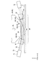
露光装置EXは、投影光学系PLと基板Pとの間の空間56の液体50中の気泡を検出する気泡検出器20を備えている。気泡検出器20は液体50中の気泡を光学的に検出するものであって、空間56の液体50に検出光を投射する投射系21と、空間56の液体50からの検出光を受光する受光系22とを備えている。投射系21は検出光を基板Pの表面に対して傾斜方向から投射することにより、空間56の液体50に検出光を投射する。投射系21は、投影光学系PLの光軸AXに対して基板Pの走査方向であるX軸方向に離れた位置から検出光を基板Pの表面に対して投射する。本実施形態では、投射系21は投影光学系PLの光軸AXに対して−X方向に離れた位置に設けられ、受光系22は投影光学系PLの光軸AXに対して+X方向に離れた位置に設けられている。
The exposure apparatus EX includes a
図2は、露光装置EXの投影光学系PLの下部、液体供給装置1、及び液体回収装置2などを示す正面図である。図2において、投影光学系PLの最下端のレンズ60は、先端部60Aが走査方向に必要な部分だけを残してY軸方向(非走査方向)に細長い矩形状に形成されている。走査露光時には、先端部60Aの直下の矩形の投影領域PAにマスクMの一部のパターン像が投影され、投影光学系PLに対して、マスクMが−X方向(又は+X方向)に速度Vで移動するのに同期して、XYステージ52を介して基板Pが+X方向(又は−X方向)に速度β・V(βは投影倍率)で移動する。そして、1つのショット領域への露光終了後に、基板Pのステッピングによって次のショット領域が走査開始位置に移動し、以下、ステップ・アンド・スキャン方式で各ショット領域に対する露光処理が順次行われる。本実施形態では、基板Pの走査方向と平行に液体50を流すように設定されている。
FIG. 2 is a front view showing the lower part of the projection optical system PL of the exposure apparatus EX, the
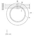
図3は、投影光学系PLのレンズ60の先端部60Aと、液体50をX軸方向に供給する供給ノズル4(4A〜4C)と、液体50を回収する回収ノズル5(5A、5B)との位置関係を示す図である。図3において、レンズ60の先端部60Aの形状はY軸方向に細長い矩形状となっており、投影光学系PLのレンズ60の先端部60AをX軸方向に挟むように、+X方向側に3つの供給ノズル4A〜4Cが配置され、−X方向側に2つの回収ノズル5A、5Bが配置されている。そして、供給ノズル4A〜4Cは供給管3を介して液体供給装置1に接続され、回収ノズル5A、5Bは回収管4を介して液体回収装置2に接続されている。また、供給ノズル4A〜4Cと回収ノズル5A、5Bとをほぼ180°回転した配置に、供給ノズル8A〜8Cと、回収ノズル9A、9Bとが配置されている。供給ノズル4A〜4Cと回収ノズル9A、9BとはY軸方向に交互に配列され、供給ノズル8A〜8Cと回収ノズル5A、5BとはY軸方向に交互に配列され、供給ノズル8A〜8Cは供給管10を介して液体供給装置1に接続され、回収ノズル9A、9Bは回収管11を介して液体回収装置2に接続されている。
FIG. 3 shows a
なお、矢印Xa(図3参照)で示す走査方向(−X方向)に基板Pを移動させて走査露光を行う場合には、供給管3、供給ノズル4A〜4C、回収管4、及び回収ノズル5A、5Bを用いて、液体供給装置1及び液体回収装置2により液体50の供給及び回収が行われる。すなわち、基板Pが−X方向に移動する際には、供給管3及び供給ノズル4(4A〜4C)を介して液体供給装置1から液体50が投影光学系PLと基板Pとの間に供給されるとともに、回収ノズル5(5A、5B)、及び回収管6を介して液体50が液体回収装置2に回収され、レンズ60と基板Pとの間を満たすように−X方向に液体50が流れる。一方、矢印Xbで示す走査方向(+X方向)に基板Pを移動させて走査露光を行う場合には、供給管10、供給ノズル8A〜8C、回収管11、及び回収ノズル9A、9Bを用いて、液体供給装置1及び液体回収装置2により液体50の供給及び回収が行われる。すなわち、基板Pが+X方向に移動する際には、供給管10及び供給ノズル8(8A〜8C)を介して液体供給装置1から液体50が投影光学系PLと基板Pとの間に供給されるとともに、回収ノズル9(9A、9B)、及び回収管11を介して液体50が液体回収装置2に回収され、レンズ60と基板Pとの間を満たすように+X方向に液体50が流れる。このように、制御装置CONTは、液体供給装置1及び液体回収装置2を用いて、基板Pの移動方向に沿って基板の移動方向と同一方向に液体50を流す。この場合、例えば液体供給装置1から供給ノズル4を介して供給される液体50は基板Pの−X方向への移動に伴って空間56に引き込まれるようにして流れるので、液体供給装置1の供給エネルギーが小さくでも液体50を空間56に容易に供給できる。そして、走査方向に応じて液体50を流す方向を切り替えることにより、+X方向、又は−X方向のどちらの方向に基板Pを走査する場合にも、レンズ60の先端面7と基板Pとの間を液体50で満たすことができ、高い解像度及び広い焦点深度を得ることができる。
In addition, when performing scanning exposure by moving the substrate P in the scanning direction (−X direction) indicated by the arrow Xa (see FIG. 3), the
図4は、気泡検出器20の概略構成を示す平面図である。投射系21及び受光系22は投影光学系PLのレンズ60の先端部60A、すなわち投影光学系PLの基板P上における投影領域PAをX軸方向に挟むように設けられている。投射系21は、Y軸方向に並ぶ複数の投射部21Aを有しており、投射部21Aのそれぞれから基板Pに対して検出光が投射される。複数の投射部21Aから投射される検出光の基板P表面に対する入射角度はそれぞれ同じ角度に設定されている。受光系22は、投射系21の投射部21Aに対応する複数の受光部22Aを有している。投射部21Aのそれぞれから投射された検出光は、液体中に気泡がなければ液体50を通過して基板Pの表面で反射し、受光部22Aに受光される。
FIG. 4 is a plan view showing a schematic configuration of the
また、受光系22は、投射系21からの検出光が直接入射しない位置に配置された受光部22B、22Cを有しており、投射系21からの検出光が液体中の気泡に当たって反射する散乱光は、その受光部22B、22Cで受光(暗視野検出)される。
Further, the
投射系21から投射される複数の検出光のうち、一部の検出光L1は基板P上のうちレンズ60の先端部60Aに対応する領域(投影光学系PLの投影領域PA)に投射されるようになっており、残りの一部の検出光L2は投影領域PAのY軸方向両外側の領域に投射されるようになっている。そして、投射系21は、複数の検出光のうち少なくとも一部の検出光Leを投影領域PAのY軸方向における境界部近傍に対して投射する。ここで、レンズ60の先端部60Aと基板Pとの間、すなわち基板P上の投影領域PAに対応する部分に液体供給装置1より液体50が供給されるため、この投影領域PAに対応する部分が液浸部分となっている。
Of the plurality of detection lights projected from the
図7(a)は、基板Pの表面に付着している気泡18に対して検出光が照射される状態を側方から見た模式図、図7(b)は図7(a)の平面図である。
図7(a)に示すように、例えば検出光がスポット光であってその光束の径がD1である場合、検出光を基板Pに対して傾斜方向から投射することにより、基板P上における検出光は図7(b)に示すようにX軸方向(走査方向)を長手方向とする楕円状となる。検出光の基板P上における楕円状の検出領域の長手方向の大きさD2は上記径D1より大きい。すなわち、例えば検出光を基板Pの表面に対して垂直方向から照射した場合は検出光の検出領域のX軸方向における大きさはD1となるが、傾斜方向から検出光を照射することで、X軸方向においてD1より大きいD2の検出領域で気泡18を検出することができる。したがって、X軸方向に走査する基板P上の気泡18を検出する際、気泡18は径D1の検出領域に比べてより広い検出領域で検出されることになり、気泡検出器20は気泡18の検出精度を向上することができる。なお、ここでは検出光をスポット光として説明したが、検出光がスリット光であっても同様の効果が得られる。
FIG. 7A is a schematic view of a state in which the detection light is applied to the air bubbles 18 attached to the surface of the substrate P as viewed from the side, and FIG. 7B is a plan view of FIG. FIG.
As shown in FIG. 7A, for example, when the detection light is a spot light and the diameter of the light beam is D1, the detection light is projected on the substrate P from an oblique direction, thereby detecting the light on the substrate P. The light has an elliptical shape whose longitudinal direction is in the X-axis direction (scanning direction) as shown in FIG. The size D2 of the detection light on the substrate P in the longitudinal direction of the elliptical detection region is larger than the diameter D1. That is, for example, when the detection light is applied to the surface of the substrate P from the vertical direction, the size of the detection area of the detection light in the X-axis direction is D1. The
次に、上述した構成を有する露光装置EXを用いてマスクMのパターンを投影光学系PL及び液体50を介して基板Pに露光する手順について図5のフローチャート図を参照しながら説明する。
マスクMがマスクステージMSTにロードされるとともに、基板Pが基板ステージPSTにロードされたら、制御装置CONTは液体供給装置1及び液体回収装置2を駆動し、空間56に対する液体供給動作を開始する。これにより、投影光学系PLの下面7(先端部60A)と基板Pの投影領域PAとの間に液体50が満たされる(ステップS1)。
Next, a procedure for exposing the pattern of the mask M to the substrate P via the projection optical system PL and the liquid 50 using the exposure apparatus EX having the above-described configuration will be described with reference to the flowchart of FIG.
When the mask M is loaded on the mask stage MST and the substrate P is loaded on the substrate stage PST, the control device CONT drives the
次いで、制御装置CONTは、基板ステージPSTを駆動して基板PをX軸方向に走査しつつ、照明光学系ILからの露光光ELでマスクMを照明し、マスクMのパターンを投影光学系PL及び液体50を介して基板Pに投影する。これと同時に、制御装置CONTは投射系21より検出光を基板Pに対して傾斜方向から投射する(ステップS2)。
制御装置CONTは基板P表面のZ軸方向における位置を検出しつつ基板Pに対して露光処理する。
Next, the control device CONT illuminates the mask M with the exposure light EL from the illumination optical system IL while driving the substrate stage PST to scan the substrate P in the X-axis direction, and illuminates the pattern of the mask M with the projection optical system PL. And the liquid P is projected onto the substrate P via the liquid 50. At the same time, the control device CONT projects the detection light from the
The controller CONT performs exposure processing on the substrate P while detecting the position of the surface of the substrate P in the Z-axis direction.
投射系21から基板Pに投射された検出光は空間56に満たされている液体50中を通過し、基板P上の投影領域に投射される。ここで、図4に示すように、投影領域内の基板Pの表面に気泡18が存在(付着)している場合、気泡18に投射された検出光は散乱する。気泡18に投射された検出光の一部が散乱することで、通常では検出されない強い光が受光部22B、22Cに入射し、この検出光に対応する受光部22Aに受光される光強度が低下する。受光部22A、22B、22Cの検出結果は制御装置CONTに出力され、制御装置CONTはこの受光系22で検出される光の強度に基づいて、基板P上に気泡が存在するか否かを検出する(ステップS3)。
The detection light projected on the substrate P from the
ここで、制御装置CONTは、受光部22B、22Cで検出される光の強度に基づいて気泡18の大きさや量を求めることができる。例えば、小さい気泡はより大きな角度で光を散乱するので、制御装置CONTは、受光部22B、22Cの検出結果に基づいて、気泡18からの散乱光の方向を求めることにより、気泡18の大きさを求めることができる。更に、受光した光の強度を検出することで基板P上の単位面積当たりの気泡18の量を求めることもできる。
Here, the control device CONT can determine the size and amount of the
このとき、基板PのXY方向の位置はレーザ干渉計55の計測結果より特定されるとともに、気泡18に投射された検出光を受光した受光部22AのY軸方向における設置位置も設計値に基づいて特定される。したがって、制御装置CONTは、レーザ干渉計55の計測結果及び受光する光の強度が低下した受光部22Aの設置位置に関する情報に基づいて、基板P上において気泡18が存在する位置を特定することができる。気泡18が存在する位置を特定したら、制御装置CONTはこの気泡18の位置情報を記憶装置MRYに記憶する(ステップS4)。
At this time, the position of the substrate P in the XY directions is specified from the measurement result of the
そして、制御装置CONTは基板PをX軸方向に走査しつつ基板Pに対して検出光を投射することで、気泡18の存在の有無や気泡の量など、ショット領域のそれぞれについての気泡18に関する情報を検出することができる。
Then, the control device CONT projects the detection light onto the substrate P while scanning the substrate P in the X-axis direction, thereby controlling the presence / absence of the
ここで、記憶装置MRYには、基板Pに対して所望のパターン転写精度でパターンが転写されるかどうかの気泡18に関するしきい値情報が記憶されている。このしきい値は、気泡18の大きさに関するしきい値、あるいは1つのショット領域についての気泡18の量(数)に関するしきい値を含む。制御装置CONTは、記憶装置MRYに記憶されているしきい値情報と、気泡検出器20による気泡検出結果とを比較する(ステップS5)。
Here, the storage device MRY stores threshold information on the
制御装置CONTは、気泡検出器20による気泡検出結果が前記しきい値以上であるかどうかを判別する(ステップS6)。
例えば、径の小さい気泡18が液体50中を僅かに浮遊している場合など、気泡18が液体中に存在していても所望のパターン転写精度を得られる場合がある。そこで、気泡18の量及び大きさに関するしきい値を予め求めておき、気泡検出結果が前記しきい値以下であれば基板Pの露光を適切に行うことができると判断できる。すなわち、制御装置CONTは、記憶装置MRYに記憶されている気泡に関するしきい値情報を参照し、気泡検出器20の検出結果に基づいて、基板Pの露光が適切に行われたか否かを判断する。なお、前記しきい値は例えば予め実験的に求めることができ、記憶装置MRYに記憶されている。
The control device CONT determines whether or not the bubble detection result by the
For example, a desired pattern transfer accuracy may be obtained even when the
気泡18が上記しきい値以下であると判断したら、つまり基板Pの露光が適切に行われると判断したら、制御装置CONTは露光処理を継続する。一方、気泡18が上記しきい値以上であると判断したら、つまり、気泡18の存在により基板Pの露光が適切に行われないと判断したら、制御装置CONTは、例えば露光処理動作を中断したり、あるいは表示装置DSや不図示の警報装置を駆動して、許容範囲以上(しきい値以上)の気泡が存在する旨を通知したり、あるいは基板P上における気泡18の位置情報を表示装置DSで表示する等の処置を施す(ステップS7)。
If it is determined that the
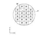
ここで、図6に示すように、基板P上の複数のショット領域SHのそれぞれについて露光する場合について考える。この場合、ステップS6において気泡18が上記しきい値以上であると判断した場合でも、制御装置CONTは露光処理を継続する。このとき、制御装置CONTは、基板P上の複数のショット領域SHのそれぞれの露光中に気泡検出器20による気泡18の検出を行い、上記しきい値情報とレーザ干渉計による気泡の位置情報とを参照し、複数のショット領域SHのうち気泡18によりパターンの像の結像が適切に行われなかったショット領域SH’を記憶装置MRYに記憶する(ステップS8)。
そして、露光処理終了後において、記憶装置MRYに記憶した情報に基づいて、複数のショット領域SHのうちパターンの像の結像が適切に行われなかったショット領域SH’は、その後に続く、別のレイヤの露光処理から除外されたり、レジストをつけ直して再露光される。
Here, as shown in FIG. 6, a case where each of the plurality of shot areas SH on the substrate P is exposed will be considered. In this case, even if it is determined in step S6 that the
After the end of the exposure processing, a shot area SH ′ of the plurality of shot areas SH where the image of the pattern was not appropriately formed based on the information stored in the storage device MRY is replaced by another shot area SH ′. Layer is excluded from the exposure processing, or the resist is re-attached and re-exposed.
本実施形態においては、複数の検出光のうち、基板P上の投影領域PAには検出光L1が投射され、Y軸方向の両側境界部に対して検出光Leが投射されている。したがって、この検出光L1やLeの受光系22での受光結果に基づいて、空間56に液体50が満たされているかどうかを判断することができる。例えば、基板P上の投影領域PAの境界部付近で液体50の剥離などの不都合が生じて空間56の一部に液体50が配置されてない状態が生じると、検出光Leの光路が変化して受光系22に受光されず、非入射状態となる。したがって、制御装置CONTは、検出光Leを受光した受光部22Aの受光結果に基づいて、空間56に液体50が満たされているかどうかを判断することができる。また、例えば、液体供給装置1が何らかの原因で動作不能となり、投影光学系PLと基板Pとの間の液体50が切れてしまう(無くなってしまう)場合も考えられる。この場合においても、検出光L1の光路が変化して受光部22Aに対して非入射状態となる。制御装置CONTは、受光部22Aの受光結果に基づいて、空間56の液体が切れるのを検出することができる。このように、気泡検出器20は、投影光学系PLと基板Pとの間の液体50が切れるのを検出する液切検出装置としての機能も有する。
In the present embodiment, of the plurality of detection lights, the detection light L1 is projected on the projection area PA on the substrate P, and the detection light Le is projected on both side boundaries in the Y-axis direction. Therefore, it is possible to determine whether or not the
この場合においても、制御装置CONTは、基板P上の複数のショット領域SHのそれぞれの露光中に液切検出装置20による液切れの検出を行い、レーザ干渉計の位置計測結果に基づいて、複数のショット領域SHのうち露光中に液切れが生じたショット領域(不良ショット領域)SH’を記憶装置MRYに記憶する。そして、露光処理終了後において、記憶装置MRYに記憶した情報に基づいて、複数のショット領域SHのうち液切れに起因してパターンの像の結像が適切に行われなかったショット領域SH’を、その後に行われる別レイヤの露光処理から除外したり、レジストをつけ直して再露光を行う。
Also in this case, the control device CONT detects the liquid shortage by the liquid
なお、上述した液切検出装置は、液切れが生じているかどうかを光学的に検出する構成であるが、例えば、液体供給装置1の供給管3や供給ノズル4に設けた流量計(流量検出装置)により液切検出装置を構成してもよい。流量検出装置は、空間56に供給される液体50の単位時間当たりの液体流量を検出し、制御装置CONTに検出結果を出力する。制御装置CONTは流量検出装置の検出結果に基づいて、液体の流量が所定値以下である場合、液切れが生じていると判断する。
Note that the above-described liquid drain detection device is configured to optically detect whether or not liquid has run out. For example, a flow meter (flow detection sensor) provided in the
また、気泡のような小さい気体部分だけでなく、比較的大きな気体の空間(気体部分)が液体中に発生してしまう場合や、液体供給装置1から液体の供給を開始したときに、投影光学系PLの像面側に気体が残ってしまう場合も考えられる。こうした場合にも、検出光L1が受光部22Aに対して非入射状態となるため、受光部22Aの受光結果に基づいて、投影光学系PLの像面側の気体部分の有無を検出することができる。このように、気泡検出器20は、液体中の気泡の検出だけでなく、投影光学系PLと基板Pとの間の気体部分の有無を検出する機能も有する。
In addition, when a relatively large gas space (gas portion) is generated in the liquid in addition to a small gas portion such as a bubble, or when the supply of the liquid from the
以上説明したように、投影光学系PLと基板Pとの間の空間56に満たされた液体50中の気泡18を検出する気泡検出器20を設けたので、パターン転写精度に大きく影響するこの空間56での気泡18の情報を検出することで良好な生産性を維持するための適切な処置を施すことができる。そして、気泡が存在した場合には、気泡検出結果に基づいてパターンが適切に転写されたかどうかを判断することで、例えばパターンが適切に転写されたショット領域に対応するデバイスのみを製品として用いたり、あるいは露光処理を一旦中断して気泡を除去するための処理を施すといった処置を施すことができる。
As described above, since the
なお、本実施形態では、基板Pの表面に付着している気泡18を検出する場合について説明したが、液体50中に気泡が浮遊している場合においても、この浮遊している気泡に検出光が照射されることにより受光系22で受光される光の強度が変化するので、液体50中に浮遊している気泡の量を検出することも可能である。また、浮遊している気泡を検出した検出光と、基板Pに付着している気泡を検出した検出光とでは受光部22B、22Cに受光される光の強度が異なるので、検出した気泡が浮遊しているものか基板Pに付着しているものかを受光部22B、22Cの受光結果に基づいて判別することも可能である。また、検出光を投影光学系PLの下面7に対して照射することにより、この投影光学系PLの下面7に付着している気泡に関する情報を検出することもできる。また、投射系21からの検出光の一部を基板Pの表面位置の検出に用いてもよい。
In the present embodiment, the case where the air bubbles 18 attached to the surface of the substrate P are detected has been described. However, even when the air bubbles are floating in the liquid 50, the detection light is applied to the floating air bubbles. Is irradiated, the intensity of light received by the
なお、本実施形態では、投射系21は基板Pの走査方向と離れた方向から基板Pに対してXZ平面と平行に検出光を投射することにより、検出精度の向上を図っているが、基板Pに対してYZ平面と平行に検出光を投射する構成とすることもできる。また、本実施形態では、基板Pに対してY軸方向に複数並んだスポット光(検出光)を照射するように説明したが、例えば1つのスポット光をY軸方向に走査しつつ、このスポット光に対して基板PをX軸方向に走査するようにしてもよい。あるいは、Y軸方向に延びるスポット光を基板Pに投射するようにしてもい。このような構成であっても、基板P表面の所定の領域に対する気泡検出動作を行うことができる。
In the present embodiment, the
また、上述の実施形態においては、基板P上に液浸領域を形成する場合について説明したが、特開2002−14005号公報、特開平11−16816号公報、特開昭57−117238号公報、特開平11−238680号公報、特開2000−97916号公報、特開平4−324923号公報などに開示されているような、基板ステージPST(Zステージ51)上の各種計測部材やセンサを用いる場合にも、投影光学系PLの像面側を液体で満たすことが考えられる。こうした計測部材やセンサで液体を介して計測を行うときに、投影光学系PLの像面側に気体部分(液中の気泡など)が存在すると計測誤差となってしまうおそれがある場合には、気泡検出器20を使って気体部分の有無などを検出するようにしてもよい。
In the above-described embodiment, the case where the liquid immersion area is formed on the substrate P has been described. However, Japanese Patent Application Laid-Open Nos. 2002-14005, 11-16816, and 57-117238, When using various measuring members and sensors on a substrate stage PST (Z stage 51) as disclosed in JP-A-11-238680, JP-A-2000-97916, JP-A-4-324923, and the like. Also, it is conceivable that the image plane side of the projection optical system PL is filled with the liquid. When performing measurement via a liquid with such a measurement member or sensor, if there is a possibility that a measurement error may occur if a gas portion (such as a bubble in the liquid) exists on the image plane side of the projection optical system PL, The presence or absence of a gas portion may be detected using the
次に、本発明の別の実施形態について図8を参照しながら説明する。以下の説明において、上述した実施形態と同一又は同等の構成部分については同一の符号を付し、その説明を簡略もしくは省略する。
図8は、投影光学系PLの先端部近傍を示す側面図である。図8において、投影光学系PLの先端部の光学素子60と基板Pとの間には液体50が満たされており、基板P上には液体50の液浸領域ARが形成されている。なお図8には、基板P上に液体50を供給する供給ノズル4及び基板P上の液体50を回収する回収ノズル5は図示されていない。
Next, another embodiment of the present invention will be described with reference to FIG. In the following description, the same or equivalent components as those of the above-described embodiment are denoted by the same reference numerals, and the description thereof will be simplified or omitted.
FIG. 8 is a side view showing the vicinity of the distal end of the projection optical system PL. In FIG. 8, the liquid 50 is filled between the substrate P and the
なお、本実施形態の以下の説明においては、基板Pが投影光学系PLの光学素子60と対向している場合について説明するが、特開2002−14005号公報、特開平11−16816号公報、特開昭57−117238号公報、特開平11−238680号公報、特開2000−97916号公報、特開平4−324923号公報などに開示されているような、基板ステージPST(Zステージ51)上の各種計測部材やセンサが投影光学系PLの光学素子60に対向している場合も同様である。
In the following description of the present embodiment, a case where the substrate P is opposed to the
露光装置EXは、基板Pの面位置情報を検出するフォーカス検出系70を備えている。フォーカス検出系70は、投影光学系PLの投影領域PAを挟んでその両側にそれぞれ設けられている投射系71と受光系72とを有し、投射系71から基板P上の液体50を介して基板P表面(露光面)に斜め方向から検出光Laを投射し、基板P上で反射した検出光(反射光)Laを受光系72で受光する。制御装置CONTは、フォーカス検出系70の動作を制御するとともに、受光系72の受光結果に基づいて、所定基準面に対する基板P表面のZ軸方向における位置(フォーカス位置)及び傾きを検出する。なお図8に示す例では、投射系71及び受光系72は投影領域PAを挟んで±X側のそれぞれにおいて投影領域PAに対して離れた位置に設けられているが、投射系71及び受光系72は投影領域PAを挟んで±Y側のそれぞれに設けられてもよい。
The exposure apparatus EX includes a
フォーカス検出系70の投射系71は複数の投射部を有し、図9に示す模式図のように、基板P上に複数の検出光Laを投射する。また受光系72は前記複数の投射部に応じた複数の受光部を有している。これにより、フォーカス検出系70は、基板P表面における例えばマトリクス状の複数の各点(各位置)での各フォーカス位置を求めることができ、求めた複数の各点でのフォーカス位置に基づいて、基板Pの傾斜方向の姿勢を求めることができる。なお、フォーカス検出系70の構成としては、例えば特開平8−37149号公報に開示されているものを用いることができる。制御装置CONTは、フォーカス検出系70の検出結果に基づいて、基板ステージ駆動装置PSTDを介して基板ステージPSTのZステージ51(図1参照)を駆動することにより、Zステージ51に保持されている基板PのZ軸方向における位置(フォーカス位置)、及びθX、θY方向における位置を制御する。すなわち、Zステージ51は、フォーカス検出系70の検出結果に基づく制御装置CONTからの指令に基づいて動作し、基板Pのフォーカス位置(Z位置)及び傾斜角を制御して基板Pの表面(露光面)を投影光学系PL及び液体50を介して形成される像面に合わせ込む。
The
図8に戻って、投影光学系PLの先端部近傍には、フォーカス検出系70の投射系71から射出された検出光Laを透過可能な第1光学部材81と、基板P上で反射した検出光Laを透過可能な第2光学部材82とが設けられている。第1光学部材81及び第2光学部材82は、投影光学系PL先端の光学素子60とは分離した状態で支持されており、第1光学部材81は光学素子60の−X側に配置され、第2光学部材82は光学素子60の+X側に配置されており、露光光ELの光路及び基板Pの移動を妨げない位置において、液浸領域ARの液体50に接触可能な位置に設けられている。
Returning to FIG. 8, near the tip of the projection optical system PL, a first
そして、図8に示すように、基板Pの露光処理中においては、投影光学系PLを通過した露光光ELの光路、つまり光学素子60と基板P(基板P上の投影領域PA)との間の露光光ELの光路が全て液体50で満たされるように、液体供給装置1(図1参照)から液体50が基板P上に供給される。また、光学素子60と基板Pとの間の露光光ELの光路の全てが液体50で満たされ、基板P上において液浸領域ARが投影領域PAの全てを覆うように所望状態に形成されたとき、その液浸領域ARを形成する液体50は第1光学部材81及び第2光学部材82の端面のそれぞれに密着(接触)するようになっている。基板P上に液浸領域ARが形成され、液体50が第1光学部材81及び第2光学部材82の端面のそれぞれに密着している状態においては、フォーカス検出系70の投射系71から射出された検出光La及びその基板P上での反射光Laの光路のうち第1光学部材81と第2光学部材82との間の光路は全て液体50で満たされる。また、検出光Laの光路の全てが液体50で満たされた状態のとき、フォーカス検出系70の投射系71から射出された検出光Laは、基板P上の投影光学系PLの投影領域PAに照射されるように設定されている。
なお、投影領域PAの外側、特に投影領域PAに対して基板Pの走査方向(X軸方向)に離れた位置に照射される検出光があってもよい。
Then, as shown in FIG. 8, during the exposure processing of the substrate P, the optical path of the exposure light EL passing through the projection optical system PL, that is, between the
Note that the detection light may be emitted to the outside of the projection area PA, particularly to a position separated from the projection area PA in the scanning direction (X-axis direction) of the substrate P.
液浸領域ARが所望状態で形成され、第1光学部材81と第2光学部材82との間における検出光Laの光路の全てが液体50で満たされた状態においては、フォーカス検出系70の投射系71から射出された検出光Laは、散乱や屈折などを生じることなく、第1光学部材81及び液浸領域ARの液体50を通過して基板P(投影領域PA)に所望状態で照射され、その反射光Laは、液浸領域ARの液体50及び第2光学部材82を通過して受光系72に所望状態で受光される。換言すれば、フォーカス検出系70の投射系71から射出された検出光Laが受光系72に受光されるとき、液浸領域ARは所望状態に形成されている。このように、フォーカス検出系70の受光系72の出力に基づいて、検出光Laの光路中の全てが液体50で満たされているか否かを光学的に検出することができる。
When the liquid immersion area AR is formed in a desired state and the entire optical path of the detection light La between the first
また上述したように、液浸領域ARが所望状態で形成されている状態においては、フォーカス検出系70の投射系71から射出された検出光Laは、投影光学系PLの投影領域PAに照射されるようになっており、投影領域PAを含む露光光ELの光路の少なくとも一部を通過するようになっている。したがって、フォーカス検出系70は、受光系72の出力に基づいて、露光光ELの光路が液体50で満たされているか否かを光学的に検出することができる。
As described above, in a state where the liquid immersion area AR is formed in a desired state, the detection light La emitted from the
なおここでは、第1光学部材81と第2光学部材82とは互いに独立した部材であるように説明したが、例えば投影光学系PLの先端部の光学素子60を囲むように環状の光学部材を配置し、その環状の光学部材の一部に検出光を照射し、液浸領域AR及び基板P表面を通過した検出光を、環状の光学部材を介して受光するようにしてもよい。光学部材を環状に設けて液浸領域ARの液体50を環状の光学部材の内側面に密着させることにより液浸領域AR2の形状を良好に維持することができる。また本実施形態においては、第1光学部材81及び第2光学部材82は投影光学系PLに対して分離しているが、投影光学系PLの光学素子60と一体で設けられていてもよい。
Here, the first
なお、上記第1、第2光学部材81、82の端面である液体接触面や、上記環状の光学部材の液体接触面を例えば親液化処理して親液性とすることにより、液浸領域ARの液体50は光学部材の液体接触面に密着し易くなるため、液浸領域ARの形状を維持し易くなる。
The liquid immersion area AR can be obtained by making the liquid contact surfaces, which are the end surfaces of the first and second
図10は、液浸領域ARの液体50中に気泡18が存在している状態を示す図である。図10に示すように、フォーカス検出系70の投射系71から射出された複数の検出光Laのうち、気泡18に当たった検出光Laは散乱や屈折などを生じる。したがって、気泡18に当たった検出光Laは、受光系72に光量を低下した状態で受光されるか、あるいはその光路を変化させるため受光されない。つまり、液体50中に気泡(気体部分)18がある場合、受光系72に受光される光強度が変化(低下)する。したがって、フォーカス検出系70は、受光系72の出力に基づいて、露光光ELの光路上に形成された液浸領域ARの液体50中に存在する気泡(気体部分)18を光学的に検出することができる。そして、液浸領域ARは露光光ELの光路上に形成されるものであり、検出光Laは露光光ELの光路の一部である投影領域PAを照射する構成であるため、フォーカス検出系70は、受光系72の出力に基づいて、露光光ELの光路中における気泡(気体部分)の有無、すなわち露光光ELの光路が液体50で満たされているか否かを検出することができる。更に、フォーカス検出系70は、液体50のうち検出光Laの光路中の気泡(気体部分)を検出することができる。
FIG. 10 is a diagram illustrating a state in which bubbles 18 are present in the liquid 50 in the liquid immersion area AR. As shown in FIG. 10, among the plurality of detection lights La emitted from the
ここで、気泡18とは、図10中、液体50中を浮遊している気泡18A、第1光学部材81の端面(液体接触面)に付着している気泡18B、第2光学部材82の端面(液体接触面)に付着している気泡18C、及び基板P上に付着している気泡(不図示)を含む。このように、液浸領域ARの液体50中に気泡18が存在する場合、フォーカス検出系70の投射系71から射出された検出光Laは、散乱や屈折などを生じ、受光系72に対する光量(受光量)を変化させるか、あるいはその光路を変化させて受光系72に受光されないので(符号Lb参照)、フォーカス検出系70は、受光系72の出力に基づいて、露光光ELの光路上に設けられている液浸領域ARの液体50中の気体部分(気泡)の有無を検出することができる。
Here, the
そして、本実施形態においては、フォーカス検出系70は、受光系72の出力に基づいて、検出光Laの光路中の気泡18を検出する構成であるため、基板P上に付着している気泡や第1、第2光学部材81、82に付着している気泡18(18B、18C)はもちろん、液浸領域ARを形成する液体50中を浮遊している気泡18(18A)も検出することができる。そのため、検出光Laの光路上であれば、液浸領域ARの液体50のうち露光光ELの光路以外の位置に存在する気泡18も検出することができる。そして、制御装置CONTは、フォーカス検出系70を使って基板Pの面位置情報を検出しつつ露光処理を行うため、フォーカス検出系70は、基板Pの露光処理中に検出光Laを投射し、露光光ELの光路上の液体50中の気体部分の有無や、検出光Laの光路中の気体部分の有無を検出することができる。もちろん、フォーカス検出系70は、露光処理以外のタイミングにおいても液浸領域ARの液体50中の気体部分の有無を検出することもできる。
In the present embodiment, the
また、フォーカス検出系70は、検出光Laの光路上であれば、液浸領域ARの液体50のうち露光光ELの光路以外の位置に存在する気泡18も検出することができるため、例えば走査露光中において露光光ELの光路以外の位置に存在する気泡18が基板Pの移動に伴って液体50中を移動して露光光ELの光路上に配置されたり基板Pや光学素子60に付着する可能性があっても、フォーカス検出系70によって、露光光ELの光路以外の位置に存在する気泡18が露光光ELの光路上に配置されたり、基板Pや光学素子60に付着する前に、その気泡18を検出することができる。したがって、露光処理中において、例えば液体50中を浮遊していた気泡18が露光光ELの光路上や基板P上に配置される前に、フォーカス検出系70の出力に基づいて、気泡18が露光光ELの光路上や基板P上に配置されることを予測し、例えば露光処理を停止したり、警報装置を駆動するなどの適切な処置を行うことができ、露光不良や不良ショットが発生する不都合を回避することができる。
In addition, the
また、フォーカス検出系70の投射系71は複数の検出光Laを基板P上のマトリクス状の各点に照射するため、受光系72に受光される複数の検出光Laそれぞれの光強度(受光量)に基づいて、フォーカス検出系70は気泡18の位置情報を求めることができる。ここで、複数の検出光Laそれぞれの照射位置情報は設計値に基づいて特定される。したがって、制御装置CONTは、複数の検出光Laのうち受光系72の各受光部に入射する光強度を低下させた検出光Laの照射位置情報、あるいはその検出光Laに対応する受光系72の受光部の設置位置に関する情報に基づいて、気泡18の位置(気泡18が存在した検出光の光路)を特定することができる。
In addition, since the
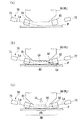
また、図11の模式図に示すように、投影光学系PLの光学素子60と基板Pとの間に液体50が十分に満たされずに液体50の一部が切れて液浸領域ARが所望状態で形成されない状況が発生し、露光光ELの光路中に気体領域AGが生成される可能性があるが、フォーカス検出系70は、その気体領域AGの有無を検出することもできる。なお気体領域AGは、例えば基板Pの移動に伴う液体50の剥離や液体供給装置1の動作不良などによって生じる。図11に示す例では、気体領域AGは第2光学部材82近傍に形成されており、液浸領域ARの液体50は第2光学部材82の端面に密着(接触)していない。この場合においても、フォーカス検出系70の投射系71から射出された検出光Laは、液浸領域ARの液体50と気体領域AGとの界面で散乱や屈折などを生じ、受光系72に光量を低下した状態で受光されるか、あるいは受光されない。フォーカス検出系70は、受光系72の出力に基づいて、液浸領域ARのうち露光光ELの光路中の気体領域AGの有無、すなわち露光光ELの光路が液体50で満たされているか否かを検出することができる。また、この場合においても、制御装置CONTは、フォーカス検出系70を使って基板Pの面位置情報を検出しつつ露光処理を行うため、そのフォーカス検出系70(受光系72)の出力に基づいて、基板Pの露光中に露光光ELの光路中の気体部分の有無や検出光Laの光路中の気体部分の有無を検出することができる。そして、露光処理中に気体領域AGをフォーカス検出系70で検出した場合には、制御装置CONTは、そのフォーカス検出系70の出力に基づいて、例えば露光動作を停止したり、液体供給装置1による液体供給量や液体回収装置2による液体回収量を調整して液浸領域ARを所望状態に形成する等の適切な処置を施すことができる。
Further, as shown in the schematic diagram of FIG. 11, the liquid 50 is not sufficiently filled between the
ところで、基板Pを液浸露光処理する際には、図12(a)の模式図に示すように、基板Pを基板ステージPSTにロードした後、露光処理を開始する前に、液体供給装置1及び液体回収装置2を駆動することで基板P上に液浸領域ARを形成する液浸領域形成動作が行われる。このとき、制御装置CONTは、フォーカス検出系70の投射系71より検出光Laを基板Pに照射しつつ露光処理前の液浸領域形成動作を行うことにより、そのフォーカス検出系70(受光系72)の出力に基づいて、基板Pの露光開始の適否を判断することができる。すなわち、露光処理前の液浸領域形成動作において、図12(b)に示すように、液浸領域ARが未だ十分に形成されずに気体領域AGがある場合、受光系72に達する検出光Laの光強度は低下するので、制御装置CONTは、フォーカス検出系70の受光系72の出力に基づいて、液浸領域ARは未だ十分に形成されていないと判断し、液浸露光処理を開始することは不適切であると判断する。そして、制御装置CONTは、液浸領域ARが所望状態に形成されるまで液浸領域形成動作を継続し、場合によっては液体供給装置1の液体供給量や液体回収装置2の液体回収量を変更したり基板Pの位置を動かす等の液浸領域形成動作条件を変更する。そして、図12(c)に示すように、液浸領域ARが十分に形成されて、第1光学部材81と第2光学部材82との間の検出光Laの光路が液体50で満たされた状態となると、投影光学系PLの光学素子60と基板Pとの間の露光光ELの光路も液体50で満たされたことになる。この状態においては、投射系71から射出された検出光Laは受光系72に所定の光強度で入射するので、制御装置CONTは、フォーカス検出系70の受光系72の出力に基づいて、液浸領域ARが形成されたと判断し、液浸露光処理を開始することは適切であると判断する。液浸露光処理を開始することは適切であると判断した制御装置CONTは、露光光ELの照射を開始して露光処理を行う。
When the substrate P is subjected to the liquid immersion exposure processing, as shown in the schematic diagram of FIG. 12A, after the substrate P is loaded on the substrate stage PST and before the exposure processing is started, the
ところで、上述したように、基板Pの露光中において、フォーカス検出系70によって露光光ELの光路を含む液浸領域AR中に気泡18や気体領域AG等の気体部分が検出された場合、制御装置CONTはその基板Pの露光処理を停止する等の処置を行うが、露光光ELの光路上に液体50が満たされているにも係わらず、検出光Laが受光系72に所定の光強度で受光されない状況が発生することが考えられ、その場合、液浸露光処理可能であるにも係わらず、露光処理を停止してしまう不都合が生じる。例えば図13の模式図に示すように、フォーカス検出系70の投射系71から投射された複数の検出光La1〜La5のうち、基板Pのエッジ部Eと基板Pの周りに設けられたプレート部材57との間の隙間58に照射された検出光La3は、散乱や屈折などを生じて受光系72に所定の光強度で受光されない可能性がある。ここで、プレート部材57は基板Pに同心状に設けられた環状部材であって、プレート部材57の上面と基板Pの上面とはほぼ面一となっており、このプレート部材57によって、基板Pのエッジ部E近傍を液浸露光する際にも投影光学系PLの光学素子60の下に液体50を保持して液浸領域ARの形状を維持できるようになっている。そして、基板Pとプレート部材57との間に隙間58が形成されているが、その隙間58に照射された検出光La3は、液浸領域ARが良好に形成されているにも係わらず、受光系72に所定の光強度で受光されない可能性があり、制御装置CONTは、受光系72の出力に基づいて露光処理を停止してしまう不都合が生じる。また、プレート部材57が設けられていない構成も考えられるが、その場合、基板Pと基板ステージPST(Zステージ51)との間に段差が形成され、エッジ部E近傍の基板P上には液浸領域ARが形成されているにも係わらず、基板Pの外側に照射される検出光La3、La4、La5などが受光系72に所定の光強度で受光されない可能性がある。
By the way, as described above, during exposure of the substrate P, when the
その場合、制御装置CONTは、基板Pを支持する基板ステージPSTの位置を計測するレーザ干渉計55(図1参照)の計測結果と、レーザ干渉計55で規定されるステージ座標系での基板Pのエッジ部E(隙間58)の位置情報とに基づいて、露光動作を制御する。具体的には、例えば露光処理前のアライメント処理時などにおいて、制御装置CONTは前記ステージ座標系での基板Pのエッジ部E(隙間58)の位置情報を予め求めて記憶装置MRYに記憶しておく。そして、制御装置CONTは、レーザ干渉計55により基板Pの位置情報を計測しつつ露光処理する。露光処理中において、制御装置CONTは、隙間58を含む基板Pのエッジ部E近傍に検出光Laが照射されているか否かを、記憶装置MRYに記憶されている基板Pのエッジ部Eの位置情報を参照することで判断する。そして、例えば隙間58に検出光Laが照射されていると判断したときに、受光系72に受光される検出光Laの光量が低下したりあるいは受光されない状況が生じても、制御装置CONTは、受光系72の出力を無視し、露光処理を継続する。こうすることにより、液浸露光処理が良好に行われているにも係わらず露光処理を停止してしまうといった不都合を回避できる。
In this case, the control device CONT determines the measurement result of the laser interferometer 55 (see FIG. 1) for measuring the position of the substrate stage PST supporting the substrate P, and the substrate P in the stage coordinate system defined by the
図14は、本発明の別の実施形態を示す図である。本実施形態の特徴的な部分は、フォーカス検出系70の検出光Laを透過可能な光学部材81、82が投影光学系PLの光学素子60と一体で設けられている点である。そして、フォーカス検出系70の投射系71から射出される複数の検出光Laのうち一部又は全部の検出光Laは、投影光学系PLを構成する複数の光学素子のうち一部(先端部)の光学素子60を通過するように設けられており、フォーカス検出系70は、その光学素子60を介して検出光Laを基板P上に投射する。このような構成によっても、フォーカス検出系70は、露光光ELの光路中の気体部分の有無を検出することができる。また、図14に示す例では、光学部材81、82の下端面(液体接触面)のそれぞれは、XY平面に略平行な平坦面となっており、光学素子60の先端面(下端面)とほぼ面一となっている。そして、液浸領域ARの液体50は、光学部材81、82の下端面及び光学素子60の下端面に密着するように設けられ、投影光学系PLと基板Pとの間において、広い領域に液浸領域ARが形成される。
FIG. 14 is a diagram showing another embodiment of the present invention. A characteristic part of this embodiment is that
そして、図15に示すように液浸領域ARの液体50中に気泡18が存在する場合には、上記実施形態同様、投射系71から射出された検出光Laは気泡18に当たって散乱などするため、光強度を低下した状態で受光系72に受光される。したがって、フォーカス検出系70は、受光系72の出力に基づいて、液浸領域ARのうち露光光ELの光路中や検出光Laの光路中における気泡(気体部分)18の有無を検出することができる。
Then, as shown in FIG. 15, when bubbles 18 are present in the liquid 50 in the liquid immersion area AR, the detection light La emitted from the
なおこの場合においても、光学部材81、82のそれぞれは互いに独立した部材であってもよいし、投影光学系PLの先端部の光学素子60を囲むように環状に一体で形成されてもよい。
Also in this case, each of the
上述したように、本実施形態における液体50は純水により構成されている。純水は、半導体製造工場等で容易に大量に入手できるとともに、基板P上のフォトレジストや光学素子(レンズ)等に対する悪影響がない利点がある。また、純水は環境に対する悪影響がないとともに、不純物の含有量が極めて低いため、基板Pの表面、及び投影光学系PLの先端面に設けられている光学素子の表面を洗浄する作用も期待できる。 As described above, the liquid 50 in the present embodiment is made of pure water. Pure water has the advantage that it can be easily obtained in large quantities at a semiconductor manufacturing plant or the like, and that there is no adverse effect on the photoresist on the substrate P, optical elements (lenses), and the like. In addition, since pure water has no adverse effect on the environment and has a very low impurity content, an effect of cleaning the surface of the substrate P and the surface of the optical element provided on the tip end surface of the projection optical system PL can be expected. .
そして、波長が193nm程度の露光光ELに対する純水(水)の屈折率nはほぼ1.44と言われており、露光光ELの光源としてArFエキシマレーザ光(波長193nm)を用いた場合、基板P上では1/n、すなわち約134nmに短波長化されて高い解像度が得られる。更に、焦点深度は空気中に比べて約n倍、すなわち約1.44倍に拡大されるため、空気中で使用する場合と同程度の焦点深度が確保できればよい場合には、投影光学系PLの開口数をより増加させることができ、この点でも解像度が向上する。 The refractive index n of pure water (water) with respect to the exposure light EL having a wavelength of about 193 nm is said to be approximately 1.44, and when ArF excimer laser light (wavelength 193 nm) is used as the light source of the exposure light EL, On the substrate P, the wavelength is shortened to 1 / n, that is, about 134 nm, and high resolution is obtained. Further, since the depth of focus is expanded to about n times, that is, about 1.44 times as compared with that in the air, if it is sufficient to secure the same depth of focus as used in the air, the projection optical system PL Can be further increased, and also in this respect, the resolution is improved.
本実施形態では、投影光学系PLの先端にレンズ60が取り付けられているが、投影光学系PLの先端に取り付ける光学素子としては、投影光学系PLの光学特性、例えば収差(球面収差、コマ収差等)の調整に用いる光学プレートであってもよい。あるいは露光光ELを透過可能な平行平面板であってもよい。液体50と接触する光学素子を、レンズより安価な平行平面板とすることにより、露光装置EXの運搬、組立、調整時等において投影光学系PLの透過率、基板P上での露光光ELの照度、及び照度分布の均一性を低下させる物質(例えばシリコン系有機物等)がその平行平面板に付着しても、液体50を供給する直前にその平行平面板を交換するだけでよく、液体50と接触する光学素子をレンズとする場合に比べてその交換コストが低くなるという利点がある。すなわち、露光光ELの照射によりレジストから発生する飛散粒子、または液体50中の不純物の付着などに起因して液体50に接触する光学素子の表面が汚れるため、その光学素子を定期的に交換する必要があるが、この光学素子を安価な平行平面板とすることにより、レンズに比べて交換部品のコストが低く、且つ交換に要する時間を短くすることができ、メンテナンスコスト(ランニングコスト)の上昇やスループットの低下を抑えることができる。
In the present embodiment, the
また、液体50の流れによって生じる投影光学系PLの先端の光学素子と基板Pとの間の圧力が大きい場合には、その光学素子を交換可能とするのではなく、その圧力によって光学素子が動かないように堅固に固定してもよい。 When the pressure between the optical element at the tip of the projection optical system PL and the substrate P caused by the flow of the liquid 50 is large, the optical element is not replaced but the optical element is moved by the pressure. It may be fixed firmly so that it does not occur.
なお、本実施形態では、投影光学系PLと基板P表面との間は液体50で満たされている構成であるが、例えば基板Pの表面に平行平面板からなるカバーガラスを取り付けた状態で液体50を満たす構成であってもよい。そして、本実施形態では、このカバーガラスも投影光学系PLの一部を構成する。すなわち、本実施形態において、マスクMと基板Pとの間における露光光ELの光路上に存在する全ての光学素子を投影光学系とする。 In the present embodiment, the space between the projection optical system PL and the surface of the substrate P is filled with the liquid 50. 50 may be satisfied. In the present embodiment, the cover glass also forms a part of the projection optical system PL. That is, in the present embodiment, all optical elements existing on the optical path of the exposure light EL between the mask M and the substrate P are used as projection optical systems.
なお、本実施形態の液体50は水であるが、水以外の液体であってもよい、例えば、露光光ELの光源がF2レーザである場合、このF2レーザ光は水を透過しないので、この場合、液体50としてはF2レーザ光を透過可能な例えば過フッ化ポリエーテル(PFPE)やフッ素系オイルであってもよい。また、液体50としては、その他にも、露光光ELに対する透過性があってできるだけ屈折率が高く、投影光学系PLや基板P表面に塗布されているフォトレジストに対して安定なもの(例えばセダー油)を用いることも可能である。 The liquid 50 of the present embodiment is water, a liquid other than water may be, for example, when the light source of exposure light EL is an F 2 laser, the F 2 laser beam is not transmitted through water in this case, it may be a permeable example perfluorinated polyether (PFPE) or fluorine based oil an F 2 laser light as the liquid 50. In addition, as the liquid 50, a liquid that has transparency to the exposure light EL, has a refractive index as high as possible, and is stable with respect to the photoresist applied to the projection optical system PL and the surface of the substrate P (for example, Cedar) Oil) can also be used.
なお、上記各実施形態において、上述したノズルの形状は特に限定されるものでなく、例えば先端部60Aの長辺について2対のノズルで液体50の供給又は回収を行うようにしてもよい。なお、この場合には、+X方向、又は−X方向のどちらの方向からも液体50の供給及び回収を行うことができるようにするため、供給ノズルと回収ノズルと上下に並べて配置してもよい。
In each of the above embodiments, the shape of the above-described nozzle is not particularly limited. For example, supply or recovery of the liquid 50 may be performed by two pairs of nozzles on the long side of the
なお、上記各実施形態の基板Pとしては、半導体デバイス製造用の半導体ウエハのみならず、ディスプレイデバイス用のガラス基板や、薄膜磁気ヘッド用のセラミックウエハ、あるいは露光装置で用いられるマスクまたはレチクルの原版(合成石英、シリコンウエハ)等が適用される。 The substrate P in each of the above embodiments is not limited to a semiconductor wafer for manufacturing a semiconductor device, but also a glass substrate for a display device, a ceramic wafer for a thin-film magnetic head, or an original mask or reticle used in an exposure apparatus. (Synthetic quartz, silicon wafer) and the like are applied.
また、上述の実施形態においては、投影光学系PLと基板Pとの間を局所的に液体で満たす露光装置を採用しているが、特開平6−124873号公報に開示されているような露光対象の基板を保持したステージを液槽の中で移動させる液浸露光装置や、特開平10−303114号公報に開示されているようなステージ上に所定深さの液体槽を形成し、その中に基板を保持する液浸露光装置にも本発明を適用可能である。 Further, in the above-described embodiment, the exposure device that locally fills the space between the projection optical system PL and the substrate P with a liquid is adopted. However, the exposure device disclosed in Japanese Patent Application Laid-Open No. 6-124873 is used. A liquid immersion exposure apparatus for moving a stage holding a target substrate in a liquid tank, or a liquid tank of a predetermined depth formed on a stage as disclosed in Japanese Patent Application Laid-Open No. 10-303114, in which The present invention is also applicable to a liquid immersion exposure apparatus that holds a substrate at a low temperature.
露光装置EXとしては、マスクMと基板Pとを同期移動してマスクMのパターンを走査露光するステップ・アンド・スキャン方式の走査型露光装置(スキャニングステッパ)の他に、マスクMと基板Pとを静止した状態でマスクMのパターンを一括露光し、基板Pを順次ステップ移動させるステップ・アンド・リピート方式の投影露光装置(ステッパ)にも適用することができる。また、本発明は基板P上で少なくとも2つのパターンを部分的に重ねて転写するステップ・アンド・スティッチ方式の露光装置にも適用できる。 The exposure apparatus EX includes a step-and-scan type scanning exposure apparatus (scanning stepper) that scans and exposes the pattern of the mask M by synchronously moving the mask M and the substrate P. Can be applied to a step-and-repeat type projection exposure apparatus (stepper) in which the pattern of the mask M is exposed collectively while the substrate is stationary, and the substrate P is sequentially moved stepwise. The present invention is also applicable to a step-and-stitch type exposure apparatus that transfers at least two patterns on the substrate P while partially overlapping each other.
また、本発明は、特開平10−163099号公報、特開平10−214783号公報、特表2000−505958号公報などに開示されているツインステージ型の露光装置にも適用できる。 Further, the present invention can be applied to a twin-stage type exposure apparatus disclosed in JP-A-10-163099, JP-A-10-214783, JP-T-2000-505958, and the like.
露光装置EXの種類としては、基板Pに半導体素子パターンを露光する半導体素子製造用の露光装置に限られず、液晶表示素子製造用又はディスプレイ製造用の露光装置や、薄膜磁気ヘッド、撮像素子(CCD)あるいはレチクル又はマスクなどを製造するための露光装置などにも広く適用できる。 The type of the exposure apparatus EX is not limited to an exposure apparatus for manufacturing a semiconductor element for exposing a semiconductor element pattern onto the substrate P, but may be an exposure apparatus for manufacturing a liquid crystal display element or a display, a thin film magnetic head, an imaging element (CCD). ) Or an exposure apparatus for manufacturing a reticle or a mask.
基板ステージPSTやマスクステージMSTにリニアモータ(USP5,623,853またはUSP5,528,118参照)を用いる場合は、エアベアリングを用いたエア浮上型およびローレンツ力またはリアクタンス力を用いた磁気浮上型のどちらを用いてもよい。また、各ステージPST、MSTは、ガイドに沿って移動するタイプでもよく、ガイドを設けないガイドレスタイプであってもよい。 When a linear motor (see US Pat. No. 5,623,853 or US Pat. No. 5,528,118) is used for the substrate stage PST and the mask stage MST, either an air levitation type using an air bearing or a magnetic levitation type using Lorentz force or reactance force is used. Is also good. Each of the stages PST and MST may be of a type that moves along a guide, or may be a guideless type that does not have a guide.
各ステージPST、MSTの駆動機構としては、二次元に磁石を配置した磁石ユニットと、二次元にコイルを配置した電機子ユニットとを対向させ電磁力により各ステージPST、MSTを駆動する平面モータを用いてもよい。この場合、磁石ユニットと電機子ユニットとのいずれか一方をステージPST、MSTに接続し、磁石ユニットと電機子ユニットとの他方をステージPST、MSTの移動面側に設ければよい。 As a driving mechanism of each stage PST, MST, a planar motor that drives each stage PST, MST by electromagnetic force by facing a magnet unit having a two-dimensionally arranged magnet and an armature unit having a two-dimensionally arranged coil. May be used. In this case, one of the magnet unit and the armature unit may be connected to the stages PST and MST, and the other of the magnet unit and the armature unit may be provided on the moving surface side of the stages PST and MST.
基板ステージPSTの移動により発生する反力は、投影光学系PLに伝わらないように、特開平8−166475号公報(USP5,528,118)に記載されているように、フレーム部材を用いて機械的に床(大地)に逃がしてもよい。
マスクステージMSTの移動により発生する反力は、投影光学系PLに伝わらないように、特開平8−330224号公報(US S/N 08/416,558)に記載されているように、フレーム部材を用いて機械的に床(大地)に逃がしてもよい。
As described in JP-A-8-166475 (US Pat. No. 5,528,118), a reaction force generated by the movement of the substrate stage PST is not mechanically transmitted to the projection optical system PL by using a frame member. You may escape to the floor (earth).
As described in JP-A-8-330224 (US S / N 08 / 416,558), a reaction force generated by the movement of the mask stage MST is not transmitted to the projection optical system PL by using a frame member. May be mechanically released to the floor (ground).
以上のように、本願実施形態の露光装置EXは、本願特許請求の範囲に挙げられた各構成要素を含む各種サブシステムを、所定の機械的精度、電気的精度、光学的精度を保つように、組み立てることで製造される。これら各種精度を確保するために、この組み立ての前後には、各種光学系については光学的精度を達成するための調整、各種機械系については機械的精度を達成するための調整、各種電気系については電気的精度を達成するための調整が行われる。各種サブシステムから露光装置への組み立て工程は、各種サブシステム相互の、機械的接続、電気回路の配線接続、気圧回路の配管接続等が含まれる。この各種サブシステムから露光装置への組み立て工程の前に、各サブシステム個々の組み立て工程があることはいうまでもない。各種サブシステムの露光装置への組み立て工程が終了したら、総合調整が行われ、露光装置全体としての各種精度が確保される。なお、露光装置の製造は温度およびクリーン度等が管理されたクリーンルームで行うことが望ましい。 As described above, the exposure apparatus EX according to the embodiment of the present invention controls various subsystems including the respective components described in the claims of the present application so as to maintain predetermined mechanical accuracy, electrical accuracy, and optical accuracy. Manufactured by assembling. Before and after this assembly, adjustments to achieve optical accuracy for various optical systems, adjustments to achieve mechanical accuracy for various mechanical systems, and various electric systems to ensure these various accuracy Are adjusted to achieve electrical accuracy. The process of assembling the exposure apparatus from the various subsystems includes mechanical connection, wiring connection of an electric circuit, and piping connection of a pneumatic circuit among the various subsystems. It goes without saying that there is an assembling process for each subsystem before the assembling process from these various subsystems to the exposure apparatus. When the process of assembling the various subsystems into the exposure apparatus is completed, comprehensive adjustment is performed, and various precisions of the entire exposure apparatus are secured. It is desirable that the exposure apparatus be manufactured in a clean room in which the temperature, the degree of cleanliness, and the like are controlled.
半導体デバイス等のマイクロデバイスは、図16に示すように、マイクロデバイスの機能・性能設計を行うステップ201、この設計ステップに基づいたマスク(レチクル)を製作するステップ202、デバイスの基材である基板を製造するステップ203、前述した実施形態の露光装置EXによりマスクのパターンを基板に露光する露光処理ステップ204、デバイス組み立てステップ(ダイシング工程、ボンディング工程、パッケージ工程を含む)205、検査ステップ206等を経て製造される。
As shown in FIG. 16, for a micro device such as a semiconductor device, a
1…液体供給装置、2…液体回収装置、20…気泡検出器(液切検出装置)、
21…投射系、22…受光系、50…液体、56…空間、CONT…制御装置、
EX…露光装置、PL…投影光学系、P…基板
DESCRIPTION OF
21: Projection system, 22: Light reception system, 50: Liquid, 56: Space, CONT: Control device,
EX: exposure apparatus, PL: projection optical system, P: substrate
Claims (27)
前記投影光学系と前記基板との間の液体中の気泡を検出する気泡検出器を備えたことを特徴とする露光装置。 An exposure apparatus that exposes the substrate by filling at least a portion between the projection optical system and the substrate with a liquid and projecting an image of a pattern onto the substrate through the projection optical system and the liquid.
An exposure apparatus comprising an air bubble detector for detecting air bubbles in a liquid between the projection optical system and the substrate.
前記投射系は、前記投影光学系の光軸に対して前記走査方向に離れた位置から光を投射することを特徴とする請求項3記載の露光装置。 The substrate is scanned and exposed while moving in a predetermined scanning direction,
The exposure apparatus according to claim 3, wherein the projection system projects light from a position separated in the scanning direction with respect to an optical axis of the projection optical system.
前記液体は、前記走査露光中に、前記投影光学系と前記基板との間を前記走査方向と平行に流れることを特徴とする請求項4記載の露光装置。 A supply device for supplying the liquid,
The exposure apparatus according to claim 4, wherein the liquid flows between the projection optical system and the substrate in parallel with the scanning direction during the scanning exposure.
該検出結果に基づき、前記気泡により前記パターンの像の結像が適切に行われなかったショット領域を記憶することを特徴とする請求項7記載の露光装置。 During the exposure of each of the plurality of shot areas on the substrate to perform detection of bubbles by the bubble detector,
8. The exposure apparatus according to claim 7, wherein a shot area in which the image of the pattern is not appropriately formed by the bubble based on the detection result is stored.
前記投影光学系と前記基板との間の少なくとも一部の液体が切れるのを検出する液切検出装置を備えることを特徴とする露光装置。 An exposure apparatus that exposes the substrate by filling at least a portion between the projection optical system and the substrate with a liquid and projecting an image of a pattern onto the substrate through the projection optical system and the liquid.
An exposure apparatus, comprising: a drain-off detection device that detects that at least a part of the liquid between the projection optical system and the substrate runs off.
前記露光光の光路中における気体部分の有無を検出する気体検出系を備えたことを特徴とする露光装置。 An exposure apparatus that exposes the substrate by irradiating the substrate with exposure light through a projection optical system and a liquid,
An exposure apparatus comprising a gas detection system for detecting the presence or absence of a gas portion in an optical path of the exposure light.
前記基板上の液体を介して前記基板上に検出光を投射するとともに、前記基板上で反射した検出光を受光して、前記基板の面位置を検出する面位置検出系を備え、
前記面位置検出系の出力に基づいて、前記検出光の光路中における気体部分の有無を検出することを特徴とする露光装置。 An exposure apparatus that exposes the substrate by irradiating the substrate with exposure light through a projection optical system and a liquid,
While projecting the detection light onto the substrate via the liquid on the substrate, receiving the detection light reflected on the substrate, comprising a surface position detection system for detecting the surface position of the substrate,
An exposure apparatus for detecting the presence or absence of a gas portion in an optical path of the detection light based on an output of the surface position detection system.
A device manufacturing method using the exposure apparatus according to any one of claims 1 to 26.
Priority Applications (10)
| Application Number | Priority Date | Filing Date | Title |
|---|---|---|---|
| JP2003393858A JP4352874B2 (en) | 2002-12-10 | 2003-11-25 | Exposure apparatus and device manufacturing method |
| EP03777406A EP1571699A4 (en) | 2002-12-10 | 2003-12-09 | Exposure apparatus and method for manufacturing device |
| SG200704275-7A SG158744A1 (en) | 2002-12-10 | 2003-12-09 | Exposure apparatus and method for producing device |
| KR1020057009284A KR101066084B1 (en) | 2002-12-10 | 2003-12-09 | Exposure apparatus and method for manufacturing device |
| AU2003289273A AU2003289273A1 (en) | 2002-12-10 | 2003-12-09 | Exposure apparatus and method for manufacturing device |
| PCT/JP2003/015737 WO2004053958A1 (en) | 2002-12-10 | 2003-12-09 | Exposure apparatus and method for manufacturing device |
| TW092134806A TW200421443A (en) | 2002-12-10 | 2003-12-10 | Exposure apparatus and device manufacturing method |
| US11/147,288 US7460207B2 (en) | 2002-12-10 | 2005-06-08 | Exposure apparatus and method for producing device |
| US11/345,392 US7436487B2 (en) | 2002-12-10 | 2006-02-02 | Exposure apparatus and method for producing device |
| US11/350,787 US7379158B2 (en) | 2002-12-10 | 2006-02-10 | Exposure apparatus and method for producing device |
Applications Claiming Priority (2)
| Application Number | Priority Date | Filing Date | Title |
|---|---|---|---|
| JP2002357960 | 2002-12-10 | ||
| JP2003393858A JP4352874B2 (en) | 2002-12-10 | 2003-11-25 | Exposure apparatus and device manufacturing method |
Publications (2)
| Publication Number | Publication Date |
|---|---|
| JP2004207696A true JP2004207696A (en) | 2004-07-22 |
| JP4352874B2 JP4352874B2 (en) | 2009-10-28 |
Family
ID=32510638
Family Applications (1)
| Application Number | Title | Priority Date | Filing Date |
|---|---|---|---|
| JP2003393858A Expired - Fee Related JP4352874B2 (en) | 2002-12-10 | 2003-11-25 | Exposure apparatus and device manufacturing method |
Country Status (8)
| Country | Link |
|---|---|
| US (3) | US7460207B2 (en) |
| EP (1) | EP1571699A4 (en) |
| JP (1) | JP4352874B2 (en) |
| KR (1) | KR101066084B1 (en) |
| AU (1) | AU2003289273A1 (en) |
| SG (1) | SG158744A1 (en) |
| TW (1) | TW200421443A (en) |
| WO (1) | WO2004053958A1 (en) |
Cited By (41)
| Publication number | Priority date | Publication date | Assignee | Title |
|---|---|---|---|---|
| WO2004114380A1 (en) * | 2003-06-19 | 2004-12-29 | Nikon Corporation | Exposure device and device producing method |
| WO2005010962A1 (en) * | 2003-07-28 | 2005-02-03 | Nikon Corporation | Exposure apparatus, device producing method, and exposure apparatus controlling method |
| WO2005076321A1 (en) * | 2004-02-03 | 2005-08-18 | Nikon Corporation | Exposure apparatus and method of producing device |
| WO2006013806A1 (en) * | 2004-08-03 | 2006-02-09 | Nikon Corporation | Exposure equipment, exposure method and device manufacturing method |
| WO2006019124A1 (en) * | 2004-08-18 | 2006-02-23 | Nikon Corporation | Exposure apparatus and device manufacturing method |
| WO2006027942A1 (en) * | 2004-09-06 | 2006-03-16 | Tokyo Ohka Kogyo Co., Ltd. | Immersion liquid for liquid immersion lithography process and method for forming resist pattern using such immersion liquid |
| WO2006054682A1 (en) * | 2004-11-18 | 2006-05-26 | Nikon Corporation | Position measurement method, position control method, measurement method, loading method, exposure method, exoposure apparatus, and device production method |
| WO2006062096A1 (en) * | 2004-12-07 | 2006-06-15 | Nikon Corporation | Exposure apparatus and method for manufacturing device |
| JP2006234598A (en) * | 2005-02-25 | 2006-09-07 | Nikon Corp | Surface inspection apparatus |
| WO2006106832A1 (en) * | 2005-03-30 | 2006-10-12 | Nikon Corporation | Method for determining exposure conditions, exposure method, exposure device, and apparatus for producing device |
| JP2006295107A (en) * | 2004-08-03 | 2006-10-26 | Nikon Corp | Exposing device, exposing method and device manufacturing method |
| JP2007005525A (en) * | 2005-06-23 | 2007-01-11 | Nikon Corp | Photolithography apparatus and device manufacturing method |
| JP2007005830A (en) * | 2003-07-28 | 2007-01-11 | Nikon Corp | Exposure system, exposure method, and method for manufacturing device |
| JP2007502539A (en) * | 2003-08-11 | 2007-02-08 | アドバンスト・マイクロ・ディバイシズ・インコーポレイテッド | Method and apparatus for monitoring and controlling immersion lithography system |
| JP2007081390A (en) * | 2005-08-17 | 2007-03-29 | Nikon Corp | Device for observation, device for measurement, device for exposure and method for exposure, method for producing device, substrate for producing device and device for positioning |
| JP2008010892A (en) * | 2003-06-11 | 2008-01-17 | Asml Netherlands Bv | Lithography device and method of manufacturing device |
| US7352440B2 (en) | 2004-12-10 | 2008-04-01 | Asml Netherlands B.V. | Substrate placement in immersion lithography |
| JP2008124283A (en) * | 2006-11-13 | 2008-05-29 | Nikon Corp | Exposure method and apparatus, immersion member, maintenance method for exposure apparatus, and device manufacturing method |
| JP2008160155A (en) * | 2003-05-13 | 2008-07-10 | Asml Netherlands Bv | Lithographic apparatus and method of manufacturing device |
| US7880860B2 (en) | 2004-12-20 | 2011-02-01 | Asml Netherlands B.V. | Lithographic apparatus and device manufacturing method |
| JP2011112410A (en) * | 2009-11-25 | 2011-06-09 | Hitachi High-Technologies Corp | Measuring device and total reflection fluorescence measuring device |
| US8035796B2 (en) | 2007-06-27 | 2011-10-11 | Canon Kabushiki Kaisha | Immersion exposure apparatus and device manufacturing method |
| JP2012123039A (en) * | 2010-12-06 | 2012-06-28 | Sony Corp | Microscope, region determining method, and program |
| US8319939B2 (en) | 2004-07-07 | 2012-11-27 | Asml Netherlands B.V. | Immersion lithographic apparatus and device manufacturing method detecting residual liquid |
| US8384874B2 (en) | 2004-07-12 | 2013-02-26 | Nikon Corporation | Immersion exposure apparatus and device manufacturing method to detect if liquid on base member |
| JP2013142625A (en) * | 2012-01-11 | 2013-07-22 | Yamashin-Filter Corp | Particle detector and particle detection method |
| US20130271945A1 (en) | 2004-02-06 | 2013-10-17 | Nikon Corporation | Polarization-modulating element, illumination optical apparatus, exposure apparatus, and exposure method |
| US8654305B2 (en) | 2007-02-15 | 2014-02-18 | Asml Holding N.V. | Systems and methods for insitu lens cleaning in immersion lithography |
| US8817226B2 (en) | 2007-02-15 | 2014-08-26 | Asml Holding N.V. | Systems and methods for insitu lens cleaning using ozone in immersion lithography |
| US8937704B2 (en) | 2003-07-31 | 2015-01-20 | Asml Netherlands B.V. | Lithographic apparatus and device manufacturing method involving a resistivity sensor |
| US9341954B2 (en) | 2007-10-24 | 2016-05-17 | Nikon Corporation | Optical unit, illumination optical apparatus, exposure apparatus, and device manufacturing method |
| US9423698B2 (en) | 2003-10-28 | 2016-08-23 | Nikon Corporation | Illumination optical apparatus and projection exposure apparatus |
| US9500960B2 (en) | 2003-04-11 | 2016-11-22 | Nikon Corporation | Apparatus and method for maintaining immersion fluid in the gap under the projection lens during wafer exchange in an immersion lithography machine |
| US9632431B2 (en) | 2004-02-02 | 2017-04-25 | Nikon Corporation | Lithographic apparatus and method having substrate and sensor tables |
| US9678437B2 (en) | 2003-04-09 | 2017-06-13 | Nikon Corporation | Illumination optical apparatus having distribution changing member to change light amount and polarization member to set polarization in circumference direction |
| US9678332B2 (en) | 2007-11-06 | 2017-06-13 | Nikon Corporation | Illumination apparatus, illumination method, exposure apparatus, and device manufacturing method |
| US9885872B2 (en) | 2003-11-20 | 2018-02-06 | Nikon Corporation | Illumination optical apparatus, exposure apparatus, and exposure method with optical integrator and polarization member that changes polarization state of light |
| US9891539B2 (en) | 2005-05-12 | 2018-02-13 | Nikon Corporation | Projection optical system, exposure apparatus, and exposure method |
| USRE46933E1 (en) | 2005-04-08 | 2018-07-03 | Asml Netherlands B.V. | Dual stage lithographic apparatus and device manufacturing method |
| US10101666B2 (en) | 2007-10-12 | 2018-10-16 | Nikon Corporation | Illumination optical apparatus, exposure apparatus, and device manufacturing method |
| US11187991B2 (en) | 2008-05-28 | 2021-11-30 | Asml Netherlands B.V. | Lithographic apparatus and a method of operating the apparatus |
Families Citing this family (161)
| Publication number | Priority date | Publication date | Assignee | Title |
|---|---|---|---|---|
| CN100568101C (en) | 2002-11-12 | 2009-12-09 | Asml荷兰有限公司 | Lithographic equipment and device making method |
| US10503084B2 (en) | 2002-11-12 | 2019-12-10 | Asml Netherlands B.V. | Lithographic apparatus and device manufacturing method |
| US9482966B2 (en) | 2002-11-12 | 2016-11-01 | Asml Netherlands B.V. | Lithographic apparatus and device manufacturing method |
| DE60335595D1 (en) | 2002-11-12 | 2011-02-17 | Asml Netherlands Bv | Immersion lithographic apparatus and method of making a device |
| US7110081B2 (en) | 2002-11-12 | 2006-09-19 | Asml Netherlands B.V. | Lithographic apparatus and device manufacturing method |
| SG121822A1 (en) | 2002-11-12 | 2006-05-26 | Asml Netherlands Bv | Lithographic apparatus and device manufacturing method |
| CN101382738B (en) | 2002-11-12 | 2011-01-12 | Asml荷兰有限公司 | Lithographic projection apparatus |
| SG135052A1 (en) | 2002-11-12 | 2007-09-28 | Asml Netherlands Bv | Lithographic apparatus and device manufacturing method |
| SG131766A1 (en) | 2002-11-18 | 2007-05-28 | Asml Netherlands Bv | Lithographic apparatus and device manufacturing method |
| SG121829A1 (en) | 2002-11-29 | 2006-05-26 | Asml Netherlands Bv | Lithographic apparatus and device manufacturing method |
| US7242455B2 (en) | 2002-12-10 | 2007-07-10 | Nikon Corporation | Exposure apparatus and method for producing device |
| EP3301511A1 (en) | 2003-02-26 | 2018-04-04 | Nikon Corporation | Exposure apparatus, exposure method, and method for producing device |
| EP2166413A1 (en) | 2003-04-11 | 2010-03-24 | Nikon Corporation | Cleanup method for optics in immersion lithography |
| TWI503865B (en) | 2003-05-23 | 2015-10-11 | 尼康股份有限公司 | A method of manufacturing an exposure apparatus and an element |
| TWI442694B (en) | 2003-05-30 | 2014-06-21 | Asml Netherlands Bv | Lithographic apparatus and device manufacturing method |
| US7213963B2 (en) | 2003-06-09 | 2007-05-08 | Asml Netherlands B.V. | Lithographic apparatus and device manufacturing method |
| US7317504B2 (en) * | 2004-04-08 | 2008-01-08 | Asml Netherlands B.V. | Lithographic apparatus and device manufacturing method |
| US6867844B2 (en) | 2003-06-19 | 2005-03-15 | Asml Holding N.V. | Immersion photolithography system and method using microchannel nozzles |
| US6809794B1 (en) | 2003-06-27 | 2004-10-26 | Asml Holding N.V. | Immersion photolithography system and method using inverted wafer-projection optics interface |
| EP1498778A1 (en) | 2003-06-27 | 2005-01-19 | ASML Netherlands B.V. | Lithographic apparatus and device manufacturing method |
| DE60308161T2 (en) | 2003-06-27 | 2007-08-09 | Asml Netherlands B.V. | Lithographic apparatus and method for making an article |
| EP1494074A1 (en) | 2003-06-30 | 2005-01-05 | ASML Netherlands B.V. | Lithographic apparatus and device manufacturing method |
| EP1975721A1 (en) | 2003-06-30 | 2008-10-01 | ASML Netherlands B.V. | Lithographic apparatus and device manufacturing method |
| KR101296501B1 (en) | 2003-07-09 | 2013-08-13 | 가부시키가이샤 니콘 | Exposure apparatus and method for manufacturing device |
| SG109000A1 (en) | 2003-07-16 | 2005-02-28 | Asml Netherlands Bv | Lithographic apparatus and device manufacturing method |
| EP1500982A1 (en) | 2003-07-24 | 2005-01-26 | ASML Netherlands B.V. | Lithographic apparatus and device manufacturing method |
| EP1503244A1 (en) | 2003-07-28 | 2005-02-02 | ASML Netherlands B.V. | Lithographic projection apparatus and device manufacturing method |
| US7175968B2 (en) | 2003-07-28 | 2007-02-13 | Asml Netherlands B.V. | Lithographic apparatus, device manufacturing method and a substrate |
| US8149381B2 (en) | 2003-08-26 | 2012-04-03 | Nikon Corporation | Optical element and exposure apparatus |
| EP2278402B1 (en) | 2003-08-26 | 2013-03-06 | Nikon Corporation | Exposure apparatus |
| US6954256B2 (en) | 2003-08-29 | 2005-10-11 | Asml Netherlands B.V. | Gradient immersion lithography |
| TWI263859B (en) | 2003-08-29 | 2006-10-11 | Asml Netherlands Bv | Lithographic apparatus and device manufacturing method |
| TWI245163B (en) | 2003-08-29 | 2005-12-11 | Asml Netherlands Bv | Lithographic apparatus and device manufacturing method |
| EP2261740B1 (en) | 2003-08-29 | 2014-07-09 | ASML Netherlands BV | Lithographic apparatus |
| JP4444920B2 (en) * | 2003-09-19 | 2010-03-31 | 株式会社ニコン | Exposure apparatus and device manufacturing method |
| EP1519230A1 (en) | 2003-09-29 | 2005-03-30 | ASML Netherlands B.V. | Lithographic apparatus and device manufacturing method |
| US7158211B2 (en) | 2003-09-29 | 2007-01-02 | Asml Netherlands B.V. | Lithographic apparatus and device manufacturing method |
| EP1519231B1 (en) | 2003-09-29 | 2005-12-21 | ASML Netherlands B.V. | Lithographic apparatus and device manufacturing method |
| KR101361892B1 (en) | 2003-10-08 | 2014-02-12 | 가부시키가이샤 자오 니콘 | Substrate carrying apparatus, substrate carrying method, exposure apparatus, exposure method, and method for producing device |
| EP1524558A1 (en) | 2003-10-15 | 2005-04-20 | ASML Netherlands B.V. | Lithographic apparatus and device manufacturing method |
| EP1524557A1 (en) | 2003-10-15 | 2005-04-20 | ASML Netherlands B.V. | Lithographic apparatus and device manufacturing method |
| US7411653B2 (en) | 2003-10-28 | 2008-08-12 | Asml Netherlands B.V. | Lithographic apparatus |
| US7352433B2 (en) | 2003-10-28 | 2008-04-01 | Asml Netherlands B.V. | Lithographic apparatus and device manufacturing method |
| US7528929B2 (en) | 2003-11-14 | 2009-05-05 | Asml Netherlands B.V. | Lithographic apparatus and device manufacturing method |
| US7545481B2 (en) | 2003-11-24 | 2009-06-09 | Asml Netherlands B.V. | Lithographic apparatus and device manufacturing method |
| US7394521B2 (en) * | 2003-12-23 | 2008-07-01 | Asml Netherlands B.V. | Lithographic apparatus and device manufacturing method |
| US7589818B2 (en) | 2003-12-23 | 2009-09-15 | Asml Netherlands B.V. | Lithographic apparatus, alignment apparatus, device manufacturing method, and a method of converting an apparatus |
| US7050146B2 (en) | 2004-02-09 | 2006-05-23 | Asml Netherlands B.V. | Lithographic apparatus and device manufacturing method |
| JP5076497B2 (en) | 2004-02-20 | 2012-11-21 | 株式会社ニコン | Exposure apparatus, liquid supply method and recovery method, exposure method, and device manufacturing method |
| US7227619B2 (en) | 2004-04-01 | 2007-06-05 | Asml Netherlands B.V. | Lithographic apparatus and device manufacturing method |
| US7034917B2 (en) * | 2004-04-01 | 2006-04-25 | Asml Netherlands B.V. | Lithographic apparatus, device manufacturing method and device manufactured thereby |
| US7295283B2 (en) | 2004-04-02 | 2007-11-13 | Asml Netherlands B.V. | Lithographic apparatus and device manufacturing method |
| US7898642B2 (en) | 2004-04-14 | 2011-03-01 | Asml Netherlands B.V. | Lithographic apparatus and device manufacturing method |
| US7379159B2 (en) | 2004-05-03 | 2008-05-27 | Asml Netherlands B.V. | Lithographic apparatus and device manufacturing method |
| US7616383B2 (en) | 2004-05-18 | 2009-11-10 | Asml Netherlands B.V. | Lithographic apparatus and device manufacturing method |
| US7486381B2 (en) | 2004-05-21 | 2009-02-03 | Asml Netherlands B.V. | Lithographic apparatus and device manufacturing method |
| CN103439863B (en) | 2004-06-09 | 2016-01-06 | 株式会社尼康 | Exposure device, exposure method, manufacturing method and maintaining method |
| US7481867B2 (en) | 2004-06-16 | 2009-01-27 | Edwards Limited | Vacuum system for immersion photolithography |
| US7161663B2 (en) | 2004-07-22 | 2007-01-09 | Asml Netherlands B.V. | Lithographic apparatus |
| US7304715B2 (en) | 2004-08-13 | 2007-12-04 | Asml Netherlands B.V. | Lithographic apparatus and device manufacturing method |
| US7701550B2 (en) | 2004-08-19 | 2010-04-20 | Asml Netherlands B.V. | Lithographic apparatus and device manufacturing method |
| US7144779B2 (en) | 2004-09-01 | 2006-12-05 | Micron Technology, Inc. | Method of forming epitaxial silicon-comprising material |
| WO2006029824A2 (en) * | 2004-09-16 | 2006-03-23 | Carl Zeiss Smt Ag | Monitoring element for lithographic projection systems |
| US7133114B2 (en) | 2004-09-20 | 2006-11-07 | Asml Netherlands B.V. | Lithographic apparatus and device manufacturing method |
| US7522261B2 (en) | 2004-09-24 | 2009-04-21 | Asml Netherlands B.V. | Lithographic apparatus and device manufacturing method |
| US7355674B2 (en) | 2004-09-28 | 2008-04-08 | Asml Netherlands B.V. | Lithographic apparatus, device manufacturing method and computer program product |
| US7894040B2 (en) | 2004-10-05 | 2011-02-22 | Asml Netherlands B.V. | Lithographic apparatus and device manufacturing method |
| US7385670B2 (en) * | 2004-10-05 | 2008-06-10 | Asml Netherlands B.V. | Lithographic apparatus, cleaning system and cleaning method for in situ removing contamination from a component in a lithographic apparatus |
| US7209213B2 (en) | 2004-10-07 | 2007-04-24 | Asml Netherlands B.V. | Lithographic apparatus and device manufacturing method |
| US7379155B2 (en) | 2004-10-18 | 2008-05-27 | Asml Netherlands B.V. | Lithographic apparatus and device manufacturing method |
| US7119876B2 (en) | 2004-10-18 | 2006-10-10 | Asml Netherlands B.V. | Lithographic apparatus and device manufacturing method |
| JP2006120674A (en) * | 2004-10-19 | 2006-05-11 | Canon Inc | Aligner and exposure method, and method for manufacturing device |
| US7414699B2 (en) | 2004-11-12 | 2008-08-19 | Asml Netherlands B.V. | Lithographic apparatus and device manufacturing method |
| US7251013B2 (en) | 2004-11-12 | 2007-07-31 | Asml Netherlands B.V. | Lithographic apparatus and device manufacturing method |
| US7423720B2 (en) | 2004-11-12 | 2008-09-09 | Asml Netherlands B.V. | Lithographic apparatus and device manufacturing method |
| US7583357B2 (en) | 2004-11-12 | 2009-09-01 | Asml Netherlands B.V. | Lithographic apparatus and device manufacturing method |
| US7411657B2 (en) | 2004-11-17 | 2008-08-12 | Asml Netherlands B.V. | Lithographic apparatus and device manufacturing method |
| US7145630B2 (en) | 2004-11-23 | 2006-12-05 | Asml Netherlands B.V. | Lithographic apparatus and device manufacturing method |
| US7161654B2 (en) | 2004-12-02 | 2007-01-09 | Asml Netherlands B.V. | Lithographic apparatus and device manufacturing method |
| US7446850B2 (en) | 2004-12-03 | 2008-11-04 | Asml Netherlands B.V. | Lithographic apparatus and device manufacturing method |
| US7248334B2 (en) | 2004-12-07 | 2007-07-24 | Asml Netherlands B.V. | Sensor shield |
| US7397533B2 (en) | 2004-12-07 | 2008-07-08 | Asml Netherlands B.V. | Lithographic apparatus and device manufacturing method |
| US7196770B2 (en) | 2004-12-07 | 2007-03-27 | Asml Netherlands B.V. | Prewetting of substrate before immersion exposure |
| US7365827B2 (en) | 2004-12-08 | 2008-04-29 | Asml Netherlands B.V. | Lithographic apparatus and device manufacturing method |
| JP4752473B2 (en) | 2004-12-09 | 2011-08-17 | 株式会社ニコン | Exposure apparatus, exposure method, and device manufacturing method |
| US7403261B2 (en) | 2004-12-15 | 2008-07-22 | Asml Netherlands B.V. | Lithographic apparatus and device manufacturing method |
| US7528931B2 (en) | 2004-12-20 | 2009-05-05 | Asml Netherlands B.V. | Lithographic apparatus and device manufacturing method |
| US7491661B2 (en) | 2004-12-28 | 2009-02-17 | Asml Netherlands B.V. | Device manufacturing method, top coat material and substrate |
| US7405805B2 (en) | 2004-12-28 | 2008-07-29 | Asml Netherlands B.V. | Lithographic apparatus and device manufacturing method |
| US20060147821A1 (en) | 2004-12-30 | 2006-07-06 | Asml Netherlands B.V. | Lithographic apparatus and device manufacturing method |
| DE602006012746D1 (en) | 2005-01-14 | 2010-04-22 | Asml Netherlands Bv | Lithographic apparatus and manufacturing method |
| SG124351A1 (en) | 2005-01-14 | 2006-08-30 | Asml Netherlands Bv | Lithographic apparatus and device manufacturing method |
| US8692973B2 (en) | 2005-01-31 | 2014-04-08 | Nikon Corporation | Exposure apparatus and method for producing device |
| EP3079164A1 (en) | 2005-01-31 | 2016-10-12 | Nikon Corporation | Exposure apparatus and method for producing device |
| KR101211570B1 (en) | 2005-02-10 | 2012-12-12 | 에이에스엠엘 네델란즈 비.브이. | Immersion liquid, exposure apparatus, and exposure process |
| US8018573B2 (en) | 2005-02-22 | 2011-09-13 | Asml Netherlands B.V. | Lithographic apparatus and device manufacturing method |
| US7224431B2 (en) | 2005-02-22 | 2007-05-29 | Asml Netherlands B.V. | Lithographic apparatus and device manufacturing method |
| US7378025B2 (en) | 2005-02-22 | 2008-05-27 | Asml Netherlands B.V. | Fluid filtration method, fluid filtered thereby, lithographic apparatus and device manufacturing method |
| US7428038B2 (en) | 2005-02-28 | 2008-09-23 | Asml Netherlands B.V. | Lithographic apparatus, device manufacturing method and apparatus for de-gassing a liquid |
| US7324185B2 (en) | 2005-03-04 | 2008-01-29 | Asml Netherlands B.V. | Lithographic apparatus and device manufacturing method |
| US7684010B2 (en) | 2005-03-09 | 2010-03-23 | Asml Netherlands B.V. | Lithographic apparatus, device manufacturing method, seal structure, method of removing an object and a method of sealing |
| US7330238B2 (en) | 2005-03-28 | 2008-02-12 | Asml Netherlands, B.V. | Lithographic apparatus, immersion projection apparatus and device manufacturing method |
| US7411654B2 (en) | 2005-04-05 | 2008-08-12 | Asml Netherlands B.V. | Lithographic apparatus and device manufacturing method |
| US7291850B2 (en) | 2005-04-08 | 2007-11-06 | Asml Netherlands B.V. | Lithographic apparatus and device manufacturing method |
| US20060232753A1 (en) | 2005-04-19 | 2006-10-19 | Asml Holding N.V. | Liquid immersion lithography system with tilted liquid flow |
| US7433016B2 (en) | 2005-05-03 | 2008-10-07 | Asml Netherlands B.V. | Lithographic apparatus and device manufacturing method |
| US7317507B2 (en) | 2005-05-03 | 2008-01-08 | Asml Netherlands B.V. | Lithographic apparatus and device manufacturing method |
| US8248577B2 (en) | 2005-05-03 | 2012-08-21 | Asml Netherlands B.V. | Lithographic apparatus and device manufacturing method |
| US7751027B2 (en) | 2005-06-21 | 2010-07-06 | Asml Netherlands B.V. | Lithographic apparatus and device manufacturing method |
| US7652746B2 (en) | 2005-06-21 | 2010-01-26 | Asml Netherlands B.V. | Lithographic apparatus and device manufacturing method |
| WO2007000995A1 (en) * | 2005-06-28 | 2007-01-04 | Nikon Corporation | Exposure apparatus and method, and device manufacturing method |
| US7468779B2 (en) | 2005-06-28 | 2008-12-23 | Asml Netherlands B.V. | Lithographic apparatus and device manufacturing method |
| US8693006B2 (en) | 2005-06-28 | 2014-04-08 | Nikon Corporation | Reflector, optical element, interferometer system, stage device, exposure apparatus, and device fabricating method |
| US7834974B2 (en) | 2005-06-28 | 2010-11-16 | Asml Netherlands B.V. | Lithographic apparatus and device manufacturing method |
| US7474379B2 (en) | 2005-06-28 | 2009-01-06 | Asml Netherlands B.V. | Lithographic apparatus and device manufacturing method |
| US7535644B2 (en) | 2005-08-12 | 2009-05-19 | Asml Netherlands B.V. | Lens element, lithographic apparatus, device manufacturing method, and device manufactured thereby |
| US8054445B2 (en) | 2005-08-16 | 2011-11-08 | Asml Netherlands B.V. | Lithographic apparatus and device manufacturing method |
| US7411658B2 (en) | 2005-10-06 | 2008-08-12 | Asml Netherlands B.V. | Lithographic apparatus and device manufacturing method |
| JPWO2007052659A1 (en) * | 2005-11-01 | 2009-04-30 | 株式会社ニコン | Exposure apparatus, exposure method, and device manufacturing method |
| US7804577B2 (en) | 2005-11-16 | 2010-09-28 | Asml Netherlands B.V. | Lithographic apparatus |
| US7656501B2 (en) | 2005-11-16 | 2010-02-02 | Asml Netherlands B.V. | Lithographic apparatus |
| US7864292B2 (en) | 2005-11-16 | 2011-01-04 | Asml Netherlands B.V. | Lithographic apparatus and device manufacturing method |
| US7633073B2 (en) | 2005-11-23 | 2009-12-15 | Asml Netherlands B.V. | Lithographic apparatus and device manufacturing method |
| US7773195B2 (en) | 2005-11-29 | 2010-08-10 | Asml Holding N.V. | System and method to increase surface tension and contact angle in immersion lithography |
| US8125610B2 (en) | 2005-12-02 | 2012-02-28 | ASML Metherlands B.V. | Method for preventing or reducing contamination of an immersion type projection apparatus and an immersion type lithographic apparatus |
| US7420194B2 (en) | 2005-12-27 | 2008-09-02 | Asml Netherlands B.V. | Lithographic apparatus and substrate edge seal |
| US7839483B2 (en) | 2005-12-28 | 2010-11-23 | Asml Netherlands B.V. | Lithographic apparatus, device manufacturing method and a control system |
| US7649611B2 (en) | 2005-12-30 | 2010-01-19 | Asml Netherlands B.V. | Lithographic apparatus and device manufacturing method |
| US8045134B2 (en) | 2006-03-13 | 2011-10-25 | Asml Netherlands B.V. | Lithographic apparatus, control system and device manufacturing method |
| JP4889331B2 (en) * | 2006-03-22 | 2012-03-07 | 大日本スクリーン製造株式会社 | Substrate processing apparatus and substrate processing method |
| EP2005222A4 (en) * | 2006-04-03 | 2010-07-28 | Incidence surfaces and optical windows that are solvophobic to immersion liquids | |
| US9477158B2 (en) | 2006-04-14 | 2016-10-25 | Asml Netherlands B.V. | Lithographic apparatus and device manufacturing method |
| US7969548B2 (en) | 2006-05-22 | 2011-06-28 | Asml Netherlands B.V. | Lithographic apparatus and lithographic apparatus cleaning method |
| US20070296937A1 (en) * | 2006-06-26 | 2007-12-27 | International Business Machines Corporation | Illumination light in immersion lithography stepper for particle or bubble detection |
| KR20090060270A (en) * | 2006-09-08 | 2009-06-11 | 가부시키가이샤 니콘 | Cleaning member, cleaning method and device manufacturing method |
| JP4357514B2 (en) * | 2006-09-29 | 2009-11-04 | 株式会社東芝 | Immersion exposure method |
| US8045135B2 (en) | 2006-11-22 | 2011-10-25 | Asml Netherlands B.V. | Lithographic apparatus with a fluid combining unit and related device manufacturing method |
| US9632425B2 (en) | 2006-12-07 | 2017-04-25 | Asml Holding N.V. | Lithographic apparatus, a dryer and a method of removing liquid from a surface |
| US8634053B2 (en) | 2006-12-07 | 2014-01-21 | Asml Netherlands B.V. | Lithographic apparatus and device manufacturing method |
| US7791709B2 (en) | 2006-12-08 | 2010-09-07 | Asml Netherlands B.V. | Substrate support and lithographic process |
| US7866330B2 (en) | 2007-05-04 | 2011-01-11 | Asml Netherlands B.V. | Cleaning device, a lithographic apparatus and a lithographic apparatus cleaning method |
| US8011377B2 (en) | 2007-05-04 | 2011-09-06 | Asml Netherlands B.V. | Cleaning device and a lithographic apparatus cleaning method |
| US7900641B2 (en) | 2007-05-04 | 2011-03-08 | Asml Netherlands B.V. | Cleaning device and a lithographic apparatus cleaning method |
| US8947629B2 (en) | 2007-05-04 | 2015-02-03 | Asml Netherlands B.V. | Cleaning device, a lithographic apparatus and a lithographic apparatus cleaning method |
| US20090025753A1 (en) * | 2007-07-24 | 2009-01-29 | Asml Netherlands B.V. | Lithographic Apparatus And Contamination Removal Or Prevention Method |
| US7916269B2 (en) | 2007-07-24 | 2011-03-29 | Asml Netherlands B.V. | Lithographic apparatus and contamination removal or prevention method |
| US8451427B2 (en) | 2007-09-14 | 2013-05-28 | Nikon Corporation | Illumination optical system, exposure apparatus, optical element and manufacturing method thereof, and device manufacturing method |
| NL1035942A1 (en) * | 2007-09-27 | 2009-03-30 | Asml Netherlands Bv | Lithographic Apparatus and Method of Cleaning a Lithographic Apparatus. |
| SG151198A1 (en) * | 2007-09-27 | 2009-04-30 | Asml Netherlands Bv | Methods relating to immersion lithography and an immersion lithographic apparatus |
| NL1036009A1 (en) * | 2007-10-05 | 2009-04-07 | Asml Netherlands Bv | An Immersion Lithography Apparatus. |
| CN101681123B (en) | 2007-10-16 | 2013-06-12 | 株式会社尼康 | Illumination optical system, exposure apparatus, and device manufacturing method |
| EP2179329A1 (en) | 2007-10-16 | 2010-04-28 | Nikon Corporation | Illumination optical system, exposure apparatus, and device manufacturing method |
| JP5017232B2 (en) * | 2007-10-31 | 2012-09-05 | エーエスエムエル ネザーランズ ビー.ブイ. | Cleaning apparatus and immersion lithography apparatus |
| NL1036273A1 (en) * | 2007-12-18 | 2009-06-19 | Asml Netherlands Bv | Lithographic apparatus and method of cleaning a surface or an immersion lithographic apparatus. |
| NL1036306A1 (en) | 2007-12-20 | 2009-06-23 | Asml Netherlands Bv | Lithographic apparatus and in-line cleaning apparatus. |
| US8339572B2 (en) | 2008-01-25 | 2012-12-25 | Asml Netherlands B.V. | Lithographic apparatus and device manufacturing method |
| EP2282188B1 (en) | 2008-05-28 | 2015-03-11 | Nikon Corporation | Illumination optical system and exposure apparatus |
| NL2005207A (en) | 2009-09-28 | 2011-03-29 | Asml Netherlands Bv | Heat pipe, lithographic apparatus and device manufacturing method. |
| US8946514B2 (en) * | 2009-12-28 | 2015-02-03 | E.I. Du Pont De Nemours And Company | Sorghum fertility restorer genotypes and methods of marker-assisted selection |
| EP2381310B1 (en) | 2010-04-22 | 2015-05-06 | ASML Netherlands BV | Fluid handling structure and lithographic apparatus |
| NL2006818A (en) | 2010-07-02 | 2012-01-03 | Asml Netherlands Bv | A method of adjusting speed and/or routing of a table movement plan and a lithographic apparatus. |
Family Cites Families (92)
| Publication number | Priority date | Publication date | Assignee | Title |
|---|---|---|---|---|
| US165159A (en) * | 1875-07-06 | Improvement in hydraulic hose | ||
| US4346164A (en) * | 1980-10-06 | 1982-08-24 | Werner Tabarelli | Photolithographic method for the manufacture of integrated circuits |
| US4468120A (en) * | 1981-02-04 | 1984-08-28 | Nippon Kogaku K.K. | Foreign substance inspecting apparatus |
| JPS57153433A (en) * | 1981-03-18 | 1982-09-22 | Hitachi Ltd | Manufacturing device for semiconductor |
| JPS58202448A (en) | 1982-05-21 | 1983-11-25 | Hitachi Ltd | Exposing device |
| JPS5919912A (en) | 1982-07-26 | 1984-02-01 | Hitachi Ltd | Immersion distance holding device |
| DD221563A1 (en) | 1983-09-14 | 1985-04-24 | Mikroelektronik Zt Forsch Tech | IMMERSIONS OBJECTIVE FOR THE STEP-BY-STEP PROJECTION IMAGING OF A MASK STRUCTURE |
| DD224448A1 (en) | 1984-03-01 | 1985-07-03 | Zeiss Jena Veb Carl | DEVICE FOR PHOTOLITHOGRAPHIC STRUCTURAL TRANSMISSION |
| JPS629353A (en) * | 1985-07-08 | 1987-01-17 | Fuji Photo Film Co Ltd | Bubble detecting method |
| JPS6265326A (en) | 1985-09-18 | 1987-03-24 | Hitachi Ltd | Exposure device |
| JPS63157419A (en) | 1986-12-22 | 1988-06-30 | Toshiba Corp | Fine pattern transfer apparatus |
| US5257128A (en) * | 1988-06-22 | 1993-10-26 | Board Of Regents, The University Of Texas System | Freezing/perfusion microscope stage |
| JP3158446B2 (en) * | 1990-12-13 | 2001-04-23 | 株式会社ニコン | Surface position detecting device, surface position detecting method, exposure apparatus, exposure method, and semiconductor manufacturing method |
| JPH04305915A (en) | 1991-04-02 | 1992-10-28 | Nikon Corp | Adhesion type exposure device |
| JPH04305917A (en) | 1991-04-02 | 1992-10-28 | Nikon Corp | Adhesion type exposure device |
| JPH0562877A (en) | 1991-09-02 | 1993-03-12 | Yasuko Shinohara | Optical system for lsi manufacturing contraction projection aligner by light |
| JPH05304072A (en) * | 1992-04-08 | 1993-11-16 | Nec Corp | Manufacture of semiconductor device |
| JPH05296812A (en) * | 1992-04-20 | 1993-11-12 | Hitachi Ltd | Optical-cable liquid-level gauge |
| JPH06124873A (en) * | 1992-10-09 | 1994-05-06 | Canon Inc | Liquid-soaking type projection exposure apparatus |
| JP2753930B2 (en) * | 1992-11-27 | 1998-05-20 | キヤノン株式会社 | Immersion type projection exposure equipment |
| JPH07220990A (en) * | 1994-01-28 | 1995-08-18 | Hitachi Ltd | Pattern forming method and exposure apparatus therefor |
| JPH08316125A (en) | 1995-05-19 | 1996-11-29 | Hitachi Ltd | Method and apparatus for projection exposing |
| JPH08316124A (en) * | 1995-05-19 | 1996-11-29 | Hitachi Ltd | Method and apparatus for projection exposing |
| US5825043A (en) * | 1996-10-07 | 1998-10-20 | Nikon Precision Inc. | Focusing and tilting adjustment system for lithography aligner, manufacturing apparatus or inspection apparatus |
| JPH10255319A (en) * | 1997-03-12 | 1998-09-25 | Hitachi Maxell Ltd | Master disk exposure device and method therefor |
| JP3747566B2 (en) * | 1997-04-23 | 2006-02-22 | 株式会社ニコン | Immersion exposure equipment |
| JP3817836B2 (en) * | 1997-06-10 | 2006-09-06 | 株式会社ニコン | EXPOSURE APPARATUS, ITS MANUFACTURING METHOD, EXPOSURE METHOD, AND DEVICE MANUFACTURING METHOD |
| US6330052B1 (en) * | 1997-06-13 | 2001-12-11 | Canon Kabushiki Kaisha | Exposure apparatus and its control method, stage apparatus, and device manufacturing method |
| US5900354A (en) * | 1997-07-03 | 1999-05-04 | Batchelder; John Samuel | Method for optical inspection and lithography |
| JPH11176727A (en) * | 1997-12-11 | 1999-07-02 | Nikon Corp | Projection aligner |
| AU2747999A (en) * | 1998-03-26 | 1999-10-18 | Nikon Corporation | Projection exposure method and system |
| JP2000058436A (en) * | 1998-08-11 | 2000-02-25 | Nikon Corp | Projection aligner and exposure method |
| US7187503B2 (en) * | 1999-12-29 | 2007-03-06 | Carl Zeiss Smt Ag | Refractive projection objective for immersion lithography |
| US6995930B2 (en) * | 1999-12-29 | 2006-02-07 | Carl Zeiss Smt Ag | Catadioptric projection objective with geometric beam splitting |
| JP2001282141A (en) * | 2000-03-31 | 2001-10-12 | Sony Corp | Photon control device |
| US6301055B1 (en) * | 2000-08-16 | 2001-10-09 | California Institute Of Technology | Solid immersion lens structures and methods for producing solid immersion lens structures |
| KR100866818B1 (en) * | 2000-12-11 | 2008-11-04 | 가부시키가이샤 니콘 | Projection optical system and exposure apparatus comprising the same |
| WO2002091078A1 (en) | 2001-05-07 | 2002-11-14 | Massachusetts Institute Of Technology | Methods and apparatus employing an index matching medium |
| DE10229818A1 (en) * | 2002-06-28 | 2004-01-15 | Carl Zeiss Smt Ag | Focus detection method and imaging system with focus detection system |
| DE10210899A1 (en) * | 2002-03-08 | 2003-09-18 | Zeiss Carl Smt Ag | Refractive projection lens for immersion lithography |
| US7092069B2 (en) * | 2002-03-08 | 2006-08-15 | Carl Zeiss Smt Ag | Projection exposure method and projection exposure system |
| TWI242691B (en) | 2002-08-23 | 2005-11-01 | Nikon Corp | Projection optical system and method for photolithography and exposure apparatus and method using same |
| US6954993B1 (en) * | 2002-09-30 | 2005-10-18 | Lam Research Corporation | Concentric proximity processing head |
| US6988326B2 (en) * | 2002-09-30 | 2006-01-24 | Lam Research Corporation | Phobic barrier meniscus separation and containment |
| US7093375B2 (en) * | 2002-09-30 | 2006-08-22 | Lam Research Corporation | Apparatus and method for utilizing a meniscus in substrate processing |
| US6788477B2 (en) * | 2002-10-22 | 2004-09-07 | Taiwan Semiconductor Manufacturing Co., Ltd. | Apparatus for method for immersion lithography |
| SG135052A1 (en) * | 2002-11-12 | 2007-09-28 | Asml Netherlands Bv | Lithographic apparatus and device manufacturing method |
| DE60335595D1 (en) * | 2002-11-12 | 2011-02-17 | Asml Netherlands Bv | Immersion lithographic apparatus and method of making a device |
| CN100568101C (en) * | 2002-11-12 | 2009-12-09 | Asml荷兰有限公司 | Lithographic equipment and device making method |
| CN101382738B (en) | 2002-11-12 | 2011-01-12 | Asml荷兰有限公司 | Lithographic projection apparatus |
| US7110081B2 (en) * | 2002-11-12 | 2006-09-19 | Asml Netherlands B.V. | Lithographic apparatus and device manufacturing method |
| SG121822A1 (en) * | 2002-11-12 | 2006-05-26 | Asml Netherlands Bv | Lithographic apparatus and device manufacturing method |
| SG131766A1 (en) * | 2002-11-18 | 2007-05-28 | Asml Netherlands Bv | Lithographic apparatus and device manufacturing method |
| DE10253679A1 (en) * | 2002-11-18 | 2004-06-03 | Infineon Technologies Ag | Optical arrangement used in the production of semiconductor components comprises a lens system arranged behind a mask, and a medium having a specified refractive index lying between the mask and the lens system |
| FR2847670B1 (en) * | 2002-11-26 | 2005-06-10 | Sc2N Sa | OPTICAL DETECTOR FOR THE PRESENCE OF GAS BUBBLES IN A LIQUID |
| DE10258718A1 (en) * | 2002-12-09 | 2004-06-24 | Carl Zeiss Smt Ag | Projection lens, in particular for microlithography, and method for tuning a projection lens |
| EP1429190B1 (en) * | 2002-12-10 | 2012-05-09 | Canon Kabushiki Kaisha | Exposure apparatus and method |
| JP4184346B2 (en) | 2002-12-13 | 2008-11-19 | コーニンクレッカ フィリップス エレクトロニクス エヌ ヴィ | Liquid removal in a method and apparatus for irradiating a spot on a layer |
| US7010958B2 (en) * | 2002-12-19 | 2006-03-14 | Asml Holding N.V. | High-resolution gas gauge proximity sensor |
| CN1316482C (en) | 2002-12-19 | 2007-05-16 | 皇家飞利浦电子股份有限公司 | Method and device for irradiating spots on a layer |
| KR100971441B1 (en) | 2002-12-19 | 2010-07-21 | 코닌클리케 필립스 일렉트로닉스 엔.브이. | Method and device for irradiating spots on a layer |
| US6781670B2 (en) * | 2002-12-30 | 2004-08-24 | Intel Corporation | Immersion lithography |
| TWI247339B (en) * | 2003-02-21 | 2006-01-11 | Asml Holding Nv | Lithographic printing with polarized light |
| US6943941B2 (en) * | 2003-02-27 | 2005-09-13 | Asml Netherlands B.V. | Stationary and dynamic radial transverse electric polarizer for high numerical aperture systems |
| US7206059B2 (en) * | 2003-02-27 | 2007-04-17 | Asml Netherlands B.V. | Stationary and dynamic radial transverse electric polarizer for high numerical aperture systems |
| US7029832B2 (en) * | 2003-03-11 | 2006-04-18 | Samsung Electronics Co., Ltd. | Immersion lithography methods using carbon dioxide |
| KR20050122269A (en) * | 2003-04-17 | 2005-12-28 | 가부시키가이샤 니콘 | Optical arrangement of autofocus elements for use with immersion lithography |
| JP4025683B2 (en) * | 2003-05-09 | 2007-12-26 | 松下電器産業株式会社 | Pattern forming method and exposure apparatus |
| JP4146755B2 (en) * | 2003-05-09 | 2008-09-10 | 松下電器産業株式会社 | Pattern formation method |
| EP2261742A3 (en) * | 2003-06-11 | 2011-05-25 | ASML Netherlands BV | Lithographic apparatus and device manufacturing method. |
| JP4054285B2 (en) * | 2003-06-12 | 2008-02-27 | 松下電器産業株式会社 | Pattern formation method |
| JP4084710B2 (en) * | 2003-06-12 | 2008-04-30 | 松下電器産業株式会社 | Pattern formation method |
| US6867844B2 (en) * | 2003-06-19 | 2005-03-15 | Asml Holding N.V. | Immersion photolithography system and method using microchannel nozzles |
| JP4029064B2 (en) * | 2003-06-23 | 2008-01-09 | 松下電器産業株式会社 | Pattern formation method |
| JP4084712B2 (en) * | 2003-06-23 | 2008-04-30 | 松下電器産業株式会社 | Pattern formation method |
| JP2005019616A (en) | 2003-06-25 | 2005-01-20 | Canon Inc | Immersion type exposure apparatus |
| US6809794B1 (en) * | 2003-06-27 | 2004-10-26 | Asml Holding N.V. | Immersion photolithography system and method using inverted wafer-projection optics interface |
| US7006209B2 (en) * | 2003-07-25 | 2006-02-28 | Advanced Micro Devices, Inc. | Method and apparatus for monitoring and controlling imaging in immersion lithography systems |
| US7700267B2 (en) * | 2003-08-11 | 2010-04-20 | Taiwan Semiconductor Manufacturing Company, Ltd. | Immersion fluid for immersion lithography, and method of performing immersion lithography |
| US7061578B2 (en) * | 2003-08-11 | 2006-06-13 | Advanced Micro Devices, Inc. | Method and apparatus for monitoring and controlling imaging in immersion lithography systems |
| US7579135B2 (en) * | 2003-08-11 | 2009-08-25 | Taiwan Semiconductor Manufacturing Company, Ltd. | Lithography apparatus for manufacture of integrated circuits |
| US7085075B2 (en) * | 2003-08-12 | 2006-08-01 | Carl Zeiss Smt Ag | Projection objectives including a plurality of mirrors with lenses ahead of mirror M3 |
| US7070915B2 (en) * | 2003-08-29 | 2006-07-04 | Tokyo Electron Limited | Method and system for drying a substrate |
| US6954256B2 (en) * | 2003-08-29 | 2005-10-11 | Asml Netherlands B.V. | Gradient immersion lithography |
| US7014966B2 (en) * | 2003-09-02 | 2006-03-21 | Advanced Micro Devices, Inc. | Method and apparatus for elimination of bubbles in immersion medium in immersion lithography systems |
| US6961186B2 (en) * | 2003-09-26 | 2005-11-01 | Takumi Technology Corp. | Contact printing using a magnified mask image |
| US7369217B2 (en) * | 2003-10-03 | 2008-05-06 | Micronic Laser Systems Ab | Method and device for immersion lithography |
| US7678527B2 (en) * | 2003-10-16 | 2010-03-16 | Intel Corporation | Methods and compositions for providing photoresist with improved properties for contacting liquids |
| US7924397B2 (en) * | 2003-11-06 | 2011-04-12 | Taiwan Semiconductor Manufacturing Company, Ltd. | Anti-corrosion layer on objective lens for liquid immersion lithography applications |
| US7545481B2 (en) * | 2003-11-24 | 2009-06-09 | Asml Netherlands B.V. | Lithographic apparatus and device manufacturing method |
| US7125652B2 (en) * | 2003-12-03 | 2006-10-24 | Advanced Micro Devices, Inc. | Immersion lithographic process using a conforming immersion medium |
| US7050146B2 (en) * | 2004-02-09 | 2006-05-23 | Asml Netherlands B.V. | Lithographic apparatus and device manufacturing method |
-
2003
- 2003-11-25 JP JP2003393858A patent/JP4352874B2/en not_active Expired - Fee Related
- 2003-12-09 EP EP03777406A patent/EP1571699A4/en not_active Withdrawn
- 2003-12-09 AU AU2003289273A patent/AU2003289273A1/en not_active Abandoned
- 2003-12-09 SG SG200704275-7A patent/SG158744A1/en unknown
- 2003-12-09 KR KR1020057009284A patent/KR101066084B1/en not_active IP Right Cessation
- 2003-12-09 WO PCT/JP2003/015737 patent/WO2004053958A1/en active Application Filing
- 2003-12-10 TW TW092134806A patent/TW200421443A/en not_active IP Right Cessation
-
2005
- 2005-06-08 US US11/147,288 patent/US7460207B2/en not_active Expired - Fee Related
-
2006
- 2006-02-02 US US11/345,392 patent/US7436487B2/en not_active Expired - Fee Related
- 2006-02-10 US US11/350,787 patent/US7379158B2/en not_active Expired - Fee Related
Cited By (121)
| Publication number | Priority date | Publication date | Assignee | Title |
|---|---|---|---|---|
| US9678437B2 (en) | 2003-04-09 | 2017-06-13 | Nikon Corporation | Illumination optical apparatus having distribution changing member to change light amount and polarization member to set polarization in circumference direction |
| US9885959B2 (en) | 2003-04-09 | 2018-02-06 | Nikon Corporation | Illumination optical apparatus having deflecting member, lens, polarization member to set polarization in circumference direction, and optical integrator |
| US9946163B2 (en) | 2003-04-11 | 2018-04-17 | Nikon Corporation | Apparatus and method for maintaining immersion fluid in the gap under the projection lens during wafer exchange in an immersion lithography machine |
| US9500960B2 (en) | 2003-04-11 | 2016-11-22 | Nikon Corporation | Apparatus and method for maintaining immersion fluid in the gap under the projection lens during wafer exchange in an immersion lithography machine |
| JP2008160155A (en) * | 2003-05-13 | 2008-07-10 | Asml Netherlands Bv | Lithographic apparatus and method of manufacturing device |
| US9110389B2 (en) | 2003-06-11 | 2015-08-18 | Asml Netherlands B.V. | Lithographic apparatus and device manufacturing method |
| US8363208B2 (en) | 2003-06-11 | 2013-01-29 | Asml Netherlands B.V. | Lithographic apparatus and device manufacturing method |
| US7684008B2 (en) | 2003-06-11 | 2010-03-23 | Asml Netherlands B.V. | Lithographic apparatus and device manufacturing method |
| JP4580968B2 (en) * | 2003-06-11 | 2010-11-17 | エーエスエムエル ネザーランズ ビー.ブイ. | Lithographic apparatus and device manufacturing method |
| US9964858B2 (en) | 2003-06-11 | 2018-05-08 | Asml Netherlands B.V. | Lithographic apparatus and device manufacturing method |
| JP2010239158A (en) * | 2003-06-11 | 2010-10-21 | Asml Netherlands Bv | Lithographic projection apparatus |
| JP2008010892A (en) * | 2003-06-11 | 2008-01-17 | Asml Netherlands Bv | Lithography device and method of manufacturing device |
| US9551943B2 (en) | 2003-06-19 | 2017-01-24 | Nikon Corporation | Exposure apparatus and device manufacturing method |
| US10007188B2 (en) | 2003-06-19 | 2018-06-26 | Nikon Corporation | Exposure apparatus and device manufacturing method |
| US9810995B2 (en) | 2003-06-19 | 2017-11-07 | Nikon Corporation | Exposure apparatus and device manufacturing method |
| US8436979B2 (en) | 2003-06-19 | 2013-05-07 | Nikon Corporation | Exposure apparatus, and device manufacturing method |
| WO2004114380A1 (en) * | 2003-06-19 | 2004-12-29 | Nikon Corporation | Exposure device and device producing method |
| US10191388B2 (en) | 2003-06-19 | 2019-01-29 | Nikon Corporation | Exposure apparatus, and device manufacturing method |
| JP2007005830A (en) * | 2003-07-28 | 2007-01-11 | Nikon Corp | Exposure system, exposure method, and method for manufacturing device |
| US9760026B2 (en) | 2003-07-28 | 2017-09-12 | Nikon Corporation | Exposure apparatus, method for producing device, and method for controlling exposure apparatus |
| JP4492600B2 (en) * | 2003-07-28 | 2010-06-30 | 株式会社ニコン | Exposure apparatus, exposure method, and device manufacturing method |
| WO2005010962A1 (en) * | 2003-07-28 | 2005-02-03 | Nikon Corporation | Exposure apparatus, device producing method, and exposure apparatus controlling method |
| US10185232B2 (en) | 2003-07-28 | 2019-01-22 | Nikon Corporation | Exposure apparatus, method for producing device, and method for controlling exposure apparatus |
| JP2012151493A (en) * | 2003-07-28 | 2012-08-09 | Nikon Corp | Exposure apparatus, method for manufacturing device, and method for controlling exposure apparatus |
| JP2010109393A (en) * | 2003-07-28 | 2010-05-13 | Nikon Corp | Exposure apparatus, method for manufacturing device, and method for controlling exposure apparatus |
| JP2010109392A (en) * | 2003-07-28 | 2010-05-13 | Nikon Corp | Exposure apparatus, and method for manufacturing device |
| JP2010118690A (en) * | 2003-07-28 | 2010-05-27 | Nikon Corp | Exposure apparatus, method for manufacturing device, and method for controlling exposure apparatus |
| JP2010118689A (en) * | 2003-07-28 | 2010-05-27 | Nikon Corp | Exposure apparatus, method for manufacturing device, and method for controlling exposure apparatus |
| US9285686B2 (en) | 2003-07-31 | 2016-03-15 | Asml Netherlands B.V. | Lithographic apparatus involving an immersion liquid supply system with an aperture |
| US8937704B2 (en) | 2003-07-31 | 2015-01-20 | Asml Netherlands B.V. | Lithographic apparatus and device manufacturing method involving a resistivity sensor |
| JP2007502539A (en) * | 2003-08-11 | 2007-02-08 | アドバンスト・マイクロ・ディバイシズ・インコーポレイテッド | Method and apparatus for monitoring and controlling immersion lithography system |
| US9423698B2 (en) | 2003-10-28 | 2016-08-23 | Nikon Corporation | Illumination optical apparatus and projection exposure apparatus |
| US9760014B2 (en) | 2003-10-28 | 2017-09-12 | Nikon Corporation | Illumination optical apparatus and projection exposure apparatus |
| US10281632B2 (en) | 2003-11-20 | 2019-05-07 | Nikon Corporation | Illumination optical apparatus, exposure apparatus, and exposure method with optical member with optical rotatory power to rotate linear polarization direction |
| US9885872B2 (en) | 2003-11-20 | 2018-02-06 | Nikon Corporation | Illumination optical apparatus, exposure apparatus, and exposure method with optical integrator and polarization member that changes polarization state of light |
| US9684248B2 (en) | 2004-02-02 | 2017-06-20 | Nikon Corporation | Lithographic apparatus having substrate table and sensor table to measure a patterned beam |
| US10007196B2 (en) | 2004-02-02 | 2018-06-26 | Nikon Corporation | Lithographic apparatus and method having substrate and sensor tables |
| US9632431B2 (en) | 2004-02-02 | 2017-04-25 | Nikon Corporation | Lithographic apparatus and method having substrate and sensor tables |
| US9665016B2 (en) | 2004-02-02 | 2017-05-30 | Nikon Corporation | Lithographic apparatus and method having substrate table and sensor table to hold immersion liquid |
| US10139737B2 (en) | 2004-02-02 | 2018-11-27 | Nikon Corporation | Lithographic apparatus and method having substrate and sensor tables |
| JP2010103576A (en) * | 2004-02-03 | 2010-05-06 | Nikon Corp | Exposure apparatus and device manufacturing method |
| JP2011160000A (en) * | 2004-02-03 | 2011-08-18 | Nikon Corp | Exposure apparatus and method of manufacturing device |
| WO2005076321A1 (en) * | 2004-02-03 | 2005-08-18 | Nikon Corporation | Exposure apparatus and method of producing device |
| JPWO2005076321A1 (en) * | 2004-02-03 | 2008-01-10 | 株式会社ニコン | Exposure apparatus and device manufacturing method |
| JP4506674B2 (en) * | 2004-02-03 | 2010-07-21 | 株式会社ニコン | Exposure apparatus and device manufacturing method |
| KR101227211B1 (en) | 2004-02-03 | 2013-01-28 | 가부시키가이샤 니콘 | Exposure apparatus and method of producing device |
| US10151983B2 (en) | 2004-02-03 | 2018-12-11 | Nikon Corporation | Exposure apparatus and device manufacturing method |
| JP2012134553A (en) * | 2004-02-03 | 2012-07-12 | Nikon Corp | Exposure device and device manufacturing method |
| US20130271945A1 (en) | 2004-02-06 | 2013-10-17 | Nikon Corporation | Polarization-modulating element, illumination optical apparatus, exposure apparatus, and exposure method |
| US10007194B2 (en) | 2004-02-06 | 2018-06-26 | Nikon Corporation | Polarization-modulating element, illumination optical apparatus, exposure apparatus, and exposure method |
| US10241417B2 (en) | 2004-02-06 | 2019-03-26 | Nikon Corporation | Polarization-modulating element, illumination optical apparatus, exposure apparatus, and exposure method |
| US10234770B2 (en) | 2004-02-06 | 2019-03-19 | Nikon Corporation | Polarization-modulating element, illumination optical apparatus, exposure apparatus, and exposure method |
| US9104117B2 (en) | 2004-07-07 | 2015-08-11 | Bob Streefkerk | Lithographic apparatus having a liquid detection system |
| US10338478B2 (en) | 2004-07-07 | 2019-07-02 | Asml Netherlands B.V. | Lithographic apparatus and device manufacturing method |
| US10739684B2 (en) | 2004-07-07 | 2020-08-11 | Asml Netherlands B.V. | Lithographic apparatus and device manufacturing method |
| US8319939B2 (en) | 2004-07-07 | 2012-11-27 | Asml Netherlands B.V. | Immersion lithographic apparatus and device manufacturing method detecting residual liquid |
| US9250537B2 (en) | 2004-07-12 | 2016-02-02 | Nikon Corporation | Immersion exposure apparatus and method with detection of liquid on members of the apparatus |
| US8384874B2 (en) | 2004-07-12 | 2013-02-26 | Nikon Corporation | Immersion exposure apparatus and device manufacturing method to detect if liquid on base member |
| KR101230712B1 (en) * | 2004-08-03 | 2013-02-07 | 가부시키가이샤 니콘 | Exposure equipment, exposure method and device manufacturing method |
| KR101337007B1 (en) * | 2004-08-03 | 2013-12-06 | 가부시키가이샤 니콘 | Exposure equipment, exposure method and device manufacturing method |
| JP2006295107A (en) * | 2004-08-03 | 2006-10-26 | Nikon Corp | Exposing device, exposing method and device manufacturing method |
| JP2011097121A (en) * | 2004-08-03 | 2011-05-12 | Nikon Corp | Exposure apparatus, exposure method and device manufacturing method |
| WO2006013806A1 (en) * | 2004-08-03 | 2006-02-09 | Nikon Corporation | Exposure equipment, exposure method and device manufacturing method |
| CN102998910A (en) * | 2004-08-03 | 2013-03-27 | 株式会社尼康 | Exposure apparatus, exposure method and device manufacturing method |
| WO2006019124A1 (en) * | 2004-08-18 | 2006-02-23 | Nikon Corporation | Exposure apparatus and device manufacturing method |
| JPWO2006019124A1 (en) * | 2004-08-18 | 2008-05-08 | 株式会社ニコン | Exposure apparatus and device manufacturing method |
| WO2006027942A1 (en) * | 2004-09-06 | 2006-03-16 | Tokyo Ohka Kogyo Co., Ltd. | Immersion liquid for liquid immersion lithography process and method for forming resist pattern using such immersion liquid |
| US9298108B2 (en) | 2004-11-18 | 2016-03-29 | Nikon Corporation | Position measurement method, position control method, measurement method, loading method, exposure method and exposure apparatus, and device manufacturing method |
| US8072578B2 (en) | 2004-11-18 | 2011-12-06 | Nikon Corporation | Position measurement method, position control method, measurement method, loading method, exposure method and exposure apparatus, and device manufacturing method |
| JP2015111682A (en) * | 2004-11-18 | 2015-06-18 | 株式会社ニコン | Exposure device, exposure method and device manufacturing method |
| JP2010118684A (en) * | 2004-11-18 | 2010-05-27 | Nikon Corp | Position measurement method, position control method, measurement method, loading method, exposure method and exposure apparatus, and device manufacturing method |
| KR101452483B1 (en) | 2004-11-18 | 2014-10-21 | 가부시키가이샤 니콘 | Position measurement method, position control method, measurement method, loading method, exposure method, exoposure apparatus, and device production method |
| KR101578629B1 (en) | 2004-11-18 | 2015-12-17 | 가부시키가이샤 니콘 | Position measurement method, position control method, measurement method, loading method, exposure method, exoposure apparatus, and device production method |
| US9223230B2 (en) | 2004-11-18 | 2015-12-29 | Nikon Corporation | Position measurement method, position control method, measurement method, loading method, exposure method and exposure apparatus, and device manufacturing method |
| US9223231B2 (en) | 2004-11-18 | 2015-12-29 | Nikon Corporation | Position measurement method, position control method, measurement method, loading method, exposure method and exposure apparatus, and device manufacturing method |
| WO2006054682A1 (en) * | 2004-11-18 | 2006-05-26 | Nikon Corporation | Position measurement method, position control method, measurement method, loading method, exposure method, exoposure apparatus, and device production method |
| KR101437298B1 (en) | 2004-11-18 | 2014-09-02 | 가부시키가이샤 니콘 | Position measurement method, position control method, measurement method, loading method, exposure method, exoposure apparatus, and device production method |
| JP2018067014A (en) * | 2004-11-18 | 2018-04-26 | 株式会社ニコン | Exposure device, exposure method and semiconductor device manufacturing method |
| JP2016040624A (en) * | 2004-11-18 | 2016-03-24 | 株式会社ニコン | Exposure equipment and exposure method and device manufacturing method |
| US9857692B2 (en) | 2004-11-18 | 2018-01-02 | Nikon Corporation | Position measurement method, position control method, measurement method, loading method, exposure method and exposure apparatus, and device manufacturing method |
| JP2016075955A (en) * | 2004-11-18 | 2016-05-12 | 株式会社ニコン | Exposure apparatus, exposure method, and method for producing device |
| JP2011155285A (en) * | 2004-11-18 | 2011-08-11 | Nikon Corp | Exposure device and method of manufacturing device |
| US9348238B2 (en) | 2004-11-18 | 2016-05-24 | Niko Corporation | Position measurement method, position control method, measurement method, loading method, exposure method and exposure apparatus, and device manufacturing method |
| JPWO2006054682A1 (en) * | 2004-11-18 | 2008-06-05 | 株式会社ニコン | Position measurement method, position control method, measurement method, loading method, exposure method and exposure apparatus, and device manufacturing method |
| JP2016173607A (en) * | 2004-11-18 | 2016-09-29 | 株式会社ニコン | Exposure apparatus, exposure method, and method for manufacturing device |
| JP2019066887A (en) * | 2004-11-18 | 2019-04-25 | 株式会社ニコン | Exposure device and exposure method, and production method for semiconductor device |
| KR101421850B1 (en) | 2004-11-18 | 2014-07-24 | 가부시키가이샤 니콘 | Position measurement method, position control method, measurement method, loading method, exposure method, exoposure apparatus, and device production method |
| KR101421849B1 (en) | 2004-11-18 | 2014-07-24 | 가부시키가이샤 니콘 | Position measurement method, position control method, measurement method, loading method, exposure method, exoposure apparatus, and device production method |
| JP2014131082A (en) * | 2004-11-18 | 2014-07-10 | Nikon Corp | Exposure device |
| JP4877653B2 (en) * | 2004-11-18 | 2012-02-15 | 株式会社ニコン | Exposure apparatus and device manufacturing method |
| US8054465B2 (en) | 2004-11-18 | 2011-11-08 | Nikon Corporation | Position measurement method |
| US8059260B2 (en) | 2004-11-18 | 2011-11-15 | Nikon Corporation | Position measurement method, position control method, measurement method, loading method, exposure method and exposure apparatus, and device manufacturing method |
| US10222708B2 (en) | 2004-11-18 | 2019-03-05 | Nikon Corporation | Position measurement method, position control method, measurement method, loading method, exposure method and exposure apparatus, and device manufacturing method |
| KR101493641B1 (en) | 2004-11-18 | 2015-02-13 | 가부시키가이샤 니콘 | Position measurement method, position control method, measurement method, loading method, exposure method, exoposure apparatus, and device production method |
| US8576379B2 (en) | 2004-11-18 | 2013-11-05 | Nikon Corporation | Position measurement method, position control method, measurement method, loading method, exposure method and exposure apparatus, and device manufacturing method |
| WO2006062096A1 (en) * | 2004-12-07 | 2006-06-15 | Nikon Corporation | Exposure apparatus and method for manufacturing device |
| US7352440B2 (en) | 2004-12-10 | 2008-04-01 | Asml Netherlands B.V. | Substrate placement in immersion lithography |
| US8077291B2 (en) | 2004-12-10 | 2011-12-13 | Asml Netherlands B.V. | Substrate placement in immersion lithography |
| US7880860B2 (en) | 2004-12-20 | 2011-02-01 | Asml Netherlands B.V. | Lithographic apparatus and device manufacturing method |
| JP2006234598A (en) * | 2005-02-25 | 2006-09-07 | Nikon Corp | Surface inspection apparatus |
| WO2006106832A1 (en) * | 2005-03-30 | 2006-10-12 | Nikon Corporation | Method for determining exposure conditions, exposure method, exposure device, and apparatus for producing device |
| JPWO2006106832A1 (en) * | 2005-03-30 | 2008-09-11 | 株式会社ニコン | Exposure condition determination method, exposure method and exposure apparatus, and device manufacturing method |
| US9239524B2 (en) | 2005-03-30 | 2016-01-19 | Nikon Corporation | Exposure condition determination method, exposure method, exposure apparatus, and device manufacturing method involving detection of the situation of a liquid immersion region |
| JP4605219B2 (en) * | 2005-03-30 | 2011-01-05 | 株式会社ニコン | Exposure condition determination method, exposure method and exposure apparatus, and device manufacturing method |
| USRE47943E1 (en) | 2005-04-08 | 2020-04-14 | Asml Netherlands B.V. | Dual stage lithographic apparatus and device manufacturing method |
| USRE46933E1 (en) | 2005-04-08 | 2018-07-03 | Asml Netherlands B.V. | Dual stage lithographic apparatus and device manufacturing method |
| US9891539B2 (en) | 2005-05-12 | 2018-02-13 | Nikon Corporation | Projection optical system, exposure apparatus, and exposure method |
| JP2007005525A (en) * | 2005-06-23 | 2007-01-11 | Nikon Corp | Photolithography apparatus and device manufacturing method |
| JP2007081390A (en) * | 2005-08-17 | 2007-03-29 | Nikon Corp | Device for observation, device for measurement, device for exposure and method for exposure, method for producing device, substrate for producing device and device for positioning |
| JP2008124283A (en) * | 2006-11-13 | 2008-05-29 | Nikon Corp | Exposure method and apparatus, immersion member, maintenance method for exposure apparatus, and device manufacturing method |
| US8817226B2 (en) | 2007-02-15 | 2014-08-26 | Asml Holding N.V. | Systems and methods for insitu lens cleaning using ozone in immersion lithography |
| US8654305B2 (en) | 2007-02-15 | 2014-02-18 | Asml Holding N.V. | Systems and methods for insitu lens cleaning in immersion lithography |
| US8035796B2 (en) | 2007-06-27 | 2011-10-11 | Canon Kabushiki Kaisha | Immersion exposure apparatus and device manufacturing method |
| US10101666B2 (en) | 2007-10-12 | 2018-10-16 | Nikon Corporation | Illumination optical apparatus, exposure apparatus, and device manufacturing method |
| US9341954B2 (en) | 2007-10-24 | 2016-05-17 | Nikon Corporation | Optical unit, illumination optical apparatus, exposure apparatus, and device manufacturing method |
| US9857599B2 (en) | 2007-10-24 | 2018-01-02 | Nikon Corporation | Optical unit, illumination optical apparatus, exposure apparatus, and device manufacturing method |
| US9678332B2 (en) | 2007-11-06 | 2017-06-13 | Nikon Corporation | Illumination apparatus, illumination method, exposure apparatus, and device manufacturing method |
| US11187991B2 (en) | 2008-05-28 | 2021-11-30 | Asml Netherlands B.V. | Lithographic apparatus and a method of operating the apparatus |
| JP2011112410A (en) * | 2009-11-25 | 2011-06-09 | Hitachi High-Technologies Corp | Measuring device and total reflection fluorescence measuring device |
| JP2012123039A (en) * | 2010-12-06 | 2012-06-28 | Sony Corp | Microscope, region determining method, and program |
| JP2013142625A (en) * | 2012-01-11 | 2013-07-22 | Yamashin-Filter Corp | Particle detector and particle detection method |
Also Published As
| Publication number | Publication date |
|---|---|
| US7460207B2 (en) | 2008-12-02 |
| US20060126044A1 (en) | 2006-06-15 |
| AU2003289273A1 (en) | 2004-06-30 |
| EP1571699A1 (en) | 2005-09-07 |
| US20050264774A1 (en) | 2005-12-01 |
| KR101066084B1 (en) | 2011-09-20 |
| EP1571699A4 (en) | 2007-10-31 |
| US20060126043A1 (en) | 2006-06-15 |
| US7379158B2 (en) | 2008-05-27 |
| SG158744A1 (en) | 2010-02-26 |
| WO2004053958A1 (en) | 2004-06-24 |
| US7436487B2 (en) | 2008-10-14 |
| KR20050085134A (en) | 2005-08-29 |
| TW200421443A (en) | 2004-10-16 |
| TWI331357B (en) | 2010-10-01 |
| JP4352874B2 (en) | 2009-10-28 |
Similar Documents
| Publication | Publication Date | Title |
|---|---|---|
| JP4352874B2 (en) | Exposure apparatus and device manufacturing method | |
| JP4232449B2 (en) | Exposure method, exposure apparatus, and device manufacturing method | |
| US8023100B2 (en) | Exposure apparatus, supply method and recovery method, exposure method, and device producing method | |
| US7834976B2 (en) | Exposure apparatus and method for producing device | |
| US9110381B2 (en) | Substrate conveyance device and substrate conveyance method, exposure apparatus and exposure method, device manufacturing method | |
| JP4565270B2 (en) | Exposure method, device manufacturing method | |
| JP4655763B2 (en) | Exposure apparatus, exposure method, and device manufacturing method | |
| JP4720747B2 (en) | Exposure apparatus, exposure method, and device manufacturing method | |
| JP2010118714A (en) | Exposure apparatus, exposure method, and method for manufacturing device | |
| JP2010199615A (en) | Exposure method, aligner and device manufacturing method | |
| JP2009105472A (en) | Vacuum system, immersion exposure device and method for exposure, and method for manufacturing device | |
| WO2005076323A1 (en) | Aligner, device manufacturing method, maintenance method and aligning method | |
| JP2005012201A (en) | Exposure method, aligner and device manufacturing method | |
| JP2004207710A (en) | Exposure system, exposure method, and device-manufacturing method | |
| JP2005101488A (en) | Aligner, exposure method, and manufacturing method of device | |
| JP2005286286A (en) | Exposure method, aligner, device manufacturing method | |
| JP2005209705A (en) | Exposure device and manufacturing method for device | |
| JP4701606B2 (en) | Exposure method, exposure apparatus, and device manufacturing method | |
| WO2005106930A1 (en) | Exposure method, exposure system, and method for fabricating device | |
| JP2007027631A (en) | Exposure method, exposure apparatus, and device manufacturing method | |
| JP2005166997A (en) | Exposure system and method and device manufacturing method | |
| JP2006310587A (en) | Exposure device and device manufacturing method | |
| JP2010212695A (en) | Exposure method and apparatus, and device manufacturing method |
Legal Events
| Date | Code | Title | Description |
|---|---|---|---|
| A621 | Written request for application examination |
Free format text: JAPANESE INTERMEDIATE CODE: A621 Effective date: 20060928 |
|
| A131 | Notification of reasons for refusal |
Free format text: JAPANESE INTERMEDIATE CODE: A131 Effective date: 20080401 |
|
| A521 | Request for written amendment filed |
Free format text: JAPANESE INTERMEDIATE CODE: A523 Effective date: 20080530 |
|
| A131 | Notification of reasons for refusal |
Free format text: JAPANESE INTERMEDIATE CODE: A131 Effective date: 20090331 |
|
| A521 | Request for written amendment filed |
Free format text: JAPANESE INTERMEDIATE CODE: A523 Effective date: 20090410 |
|
| TRDD | Decision of grant or rejection written | ||
| A01 | Written decision to grant a patent or to grant a registration (utility model) |
Free format text: JAPANESE INTERMEDIATE CODE: A01 Effective date: 20090707 |
|
| A01 | Written decision to grant a patent or to grant a registration (utility model) |
Free format text: JAPANESE INTERMEDIATE CODE: A01 |
|
| A61 | First payment of annual fees (during grant procedure) |
Free format text: JAPANESE INTERMEDIATE CODE: A61 Effective date: 20090720 |
|
| R150 | Certificate of patent or registration of utility model |
Ref document number: 4352874 Country of ref document: JP Free format text: JAPANESE INTERMEDIATE CODE: R150 Free format text: JAPANESE INTERMEDIATE CODE: R150 |
|
| FPAY | Renewal fee payment (event date is renewal date of database) |
Free format text: PAYMENT UNTIL: 20120807 Year of fee payment: 3 |
|
| FPAY | Renewal fee payment (event date is renewal date of database) |
Free format text: PAYMENT UNTIL: 20120807 Year of fee payment: 3 |
|
| FPAY | Renewal fee payment (event date is renewal date of database) |
Free format text: PAYMENT UNTIL: 20150807 Year of fee payment: 6 |
|
| S531 | Written request for registration of change of domicile |
Free format text: JAPANESE INTERMEDIATE CODE: R313531 |
|
| FPAY | Renewal fee payment (event date is renewal date of database) |
Free format text: PAYMENT UNTIL: 20150807 Year of fee payment: 6 |
|
| R350 | Written notification of registration of transfer |
Free format text: JAPANESE INTERMEDIATE CODE: R350 |
|
| FPAY | Renewal fee payment (event date is renewal date of database) |
Free format text: PAYMENT UNTIL: 20150807 Year of fee payment: 6 |
|
| R250 | Receipt of annual fees |
Free format text: JAPANESE INTERMEDIATE CODE: R250 |
|
| R250 | Receipt of annual fees |
Free format text: JAPANESE INTERMEDIATE CODE: R250 |
|
| R250 | Receipt of annual fees |
Free format text: JAPANESE INTERMEDIATE CODE: R250 |
|
| R250 | Receipt of annual fees |
Free format text: JAPANESE INTERMEDIATE CODE: R250 |
|
| R250 | Receipt of annual fees |
Free format text: JAPANESE INTERMEDIATE CODE: R250 |
|
| LAPS | Cancellation because of no payment of annual fees |