JP2004201281A - Wireless lan antenna and wireless lan card provided with the same - Google Patents
Wireless lan antenna and wireless lan card provided with the same Download PDFInfo
- Publication number
- JP2004201281A JP2004201281A JP2003350451A JP2003350451A JP2004201281A JP 2004201281 A JP2004201281 A JP 2004201281A JP 2003350451 A JP2003350451 A JP 2003350451A JP 2003350451 A JP2003350451 A JP 2003350451A JP 2004201281 A JP2004201281 A JP 2004201281A
- Authority
- JP
- Japan
- Prior art keywords
- electrode
- antenna
- wireless lan
- matching
- feeding
- Prior art date
- Legal status (The legal status is an assumption and is not a legal conclusion. Google has not performed a legal analysis and makes no representation as to the accuracy of the status listed.)
- Pending
Links
- 230000005540 biological transmission Effects 0.000 claims abstract description 15
- 230000005855 radiation Effects 0.000 claims description 47
- 238000012545 processing Methods 0.000 claims description 5
- 239000004065 semiconductor Substances 0.000 claims description 4
- 229910000746 Structural steel Inorganic materials 0.000 claims description 3
- 239000000758 substrate Substances 0.000 claims description 3
- 229910000831 Steel Inorganic materials 0.000 claims description 2
- 239000010959 steel Substances 0.000 claims description 2
- 230000000694 effects Effects 0.000 abstract description 6
- 230000009977 dual effect Effects 0.000 description 14
- 230000005404 monopole Effects 0.000 description 6
- 238000010586 diagram Methods 0.000 description 4
- 238000000034 method Methods 0.000 description 4
- 229920000642 polymer Polymers 0.000 description 4
- 238000012986 modification Methods 0.000 description 3
- 230000004048 modification Effects 0.000 description 3
- 238000005476 soldering Methods 0.000 description 3
- 229910052802 copper Inorganic materials 0.000 description 2
- 238000005259 measurement Methods 0.000 description 2
- 239000002184 metal Substances 0.000 description 2
- 229910052751 metal Inorganic materials 0.000 description 2
- 238000010295 mobile communication Methods 0.000 description 2
- 230000010287 polarization Effects 0.000 description 2
- 238000003825 pressing Methods 0.000 description 2
- 238000007639 printing Methods 0.000 description 2
- 229910052709 silver Inorganic materials 0.000 description 2
- 239000000919 ceramic Substances 0.000 description 1
- 239000004020 conductor Substances 0.000 description 1
- 230000007423 decrease Effects 0.000 description 1
- 238000013461 design Methods 0.000 description 1
- 230000001747 exhibiting effect Effects 0.000 description 1
- 238000004519 manufacturing process Methods 0.000 description 1
- 239000000463 material Substances 0.000 description 1
- 238000007747 plating Methods 0.000 description 1
- 238000007650 screen-printing Methods 0.000 description 1
- 238000004904 shortening Methods 0.000 description 1
Images


Classifications
-
- H—ELECTRICITY
- H01—ELECTRIC ELEMENTS
- H01Q—ANTENNAS, i.e. RADIO AERIALS
- H01Q1/00—Details of, or arrangements associated with, antennas
- H01Q1/12—Supports; Mounting means
- H01Q1/22—Supports; Mounting means by structural association with other equipment or articles
- H01Q1/2258—Supports; Mounting means by structural association with other equipment or articles used with computer equipment
- H01Q1/2275—Supports; Mounting means by structural association with other equipment or articles used with computer equipment associated to expansion card or bus, e.g. in PCMCIA, PC cards, Wireless USB
-
- H—ELECTRICITY
- H01—ELECTRIC ELEMENTS
- H01Q—ANTENNAS, i.e. RADIO AERIALS
- H01Q1/00—Details of, or arrangements associated with, antennas
- H01Q1/12—Supports; Mounting means
- H01Q1/22—Supports; Mounting means by structural association with other equipment or articles
- H01Q1/24—Supports; Mounting means by structural association with other equipment or articles with receiving set
-
- H—ELECTRICITY
- H01—ELECTRIC ELEMENTS
- H01Q—ANTENNAS, i.e. RADIO AERIALS
- H01Q1/00—Details of, or arrangements associated with, antennas
- H01Q1/36—Structural form of radiating elements, e.g. cone, spiral, umbrella; Particular materials used therewith
- H01Q1/38—Structural form of radiating elements, e.g. cone, spiral, umbrella; Particular materials used therewith formed by a conductive layer on an insulating support
-
- H—ELECTRICITY
- H01—ELECTRIC ELEMENTS
- H01Q—ANTENNAS, i.e. RADIO AERIALS
- H01Q5/00—Arrangements for simultaneous operation of antennas on two or more different wavebands, e.g. dual-band or multi-band arrangements
- H01Q5/30—Arrangements for providing operation on different wavebands
- H01Q5/307—Individual or coupled radiating elements, each element being fed in an unspecified way
- H01Q5/342—Individual or coupled radiating elements, each element being fed in an unspecified way for different propagation modes
- H01Q5/357—Individual or coupled radiating elements, each element being fed in an unspecified way for different propagation modes using a single feed point
- H01Q5/364—Creating multiple current paths
-
- H—ELECTRICITY
- H01—ELECTRIC ELEMENTS
- H01Q—ANTENNAS, i.e. RADIO AERIALS
- H01Q9/00—Electrically-short antennas having dimensions not more than twice the operating wavelength and consisting of conductive active radiating elements
- H01Q9/04—Resonant antennas
- H01Q9/30—Resonant antennas with feed to end of elongated active element, e.g. unipole
- H01Q9/42—Resonant antennas with feed to end of elongated active element, e.g. unipole with folded element, the folded parts being spaced apart a small fraction of the operating wavelength
Landscapes
- Engineering & Computer Science (AREA)
- Computer Networks & Wireless Communication (AREA)
- Computer Hardware Design (AREA)
- General Engineering & Computer Science (AREA)
- Waveguide Aerials (AREA)
- Details Of Aerials (AREA)
- Variable-Direction Aerials And Aerial Arrays (AREA)
- Transceivers (AREA)
- Support Of Aerials (AREA)
Abstract
Description
本発明は無線LANに内蔵されるアンテナに関するもので、より詳しくは、サイズを増大させることなく高帯域(5GHz)及び低帯域(2.4GHz)の無線信号を送受信でき、構造を変更させることなく簡単にアンテナの特性調整が可能な無線LANアンテナ及びこれから具現した無線LANカードに関するものである。 The present invention relates to an antenna built in a wireless LAN, and more specifically, can transmit and receive high-band (5 GHz) and low-band (2.4 GHz) radio signals without increasing the size, and without changing the structure. The present invention relates to a wireless LAN antenna capable of easily adjusting the characteristics of the antenna and a wireless LAN card embodied therefrom.
最近、移動通信装置が小型化及び軽量化され、送受信帯域が2帯域以上に多重化されながら、移動通信端末機の無線送受信を担う重要部品の一つであるアンテナも外装型のヘリカルアンテナからF型または逆F型アンテナへと発展してきた。 Recently, as mobile communication devices have been reduced in size and weight, and transmission / reception bands have been multiplexed into two or more bands, an antenna, which is one of the important components responsible for wireless transmission / reception of mobile communication terminals, has been changed from an external helical antenna to an F-type antenna. Or inverted-F antennas.
とりわけ、無線LAN(Wireless Local Area Network)においては、現在の使用帯域である2.4GHzばかりでなく、向後マルチメディアなど大量のデータ伝送も可能にすべく5GHz帯域まで送受信できるデュアルバンド形態のアンテナが要求されている。 In particular, in a wireless LAN (Wireless Local Area Network), a dual-band antenna capable of transmitting and receiving up to a 5-GHz band in order to enable transmission of a large amount of data such as post-multimedia as well as the current band of 2.4 GHz is used. Is required.
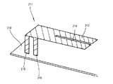
図9は従来のデュアルバンドアンテナを表すもので、図示のように、アンテナ(211)は所定の面積を有する放射電極(213)と、前記放射電極(213)の内部に位置して前記放射電極(213)の電流経路を多重化するスロット(214)と、前記放射電極(213)に電流を印加する給電電極(216)と、前記放射電極(213)を接地させる接地電極(215)とで成る。 FIG. 9 shows a conventional dual-band antenna. As shown, an antenna (211) has a radiation electrode (213) having a predetermined area and the radiation electrode (213) located inside the radiation electrode (213). A slot (214) for multiplexing the current path of (213), a feeding electrode (216) for applying a current to the radiation electrode (213), and a ground electrode (215) for grounding the radiation electrode (213). Become.
ここで、1つのスロット(214)は前記給電電極(216)を基準に放射電極(213)上に並列連結された2個の電流経路を形成し、各々の電流経路に対応する2個の周波数帯域において共振が起こるようにする。そして、前記共振の起こる2個の周波数帯域が該当アンテナの送受信帯域となる。従って、前記2個の送受信帯域は各々放射電極(213)のスロット(214)により区分された両放射領域の面積により決定される。 Here, one slot (214) forms two current paths connected in parallel on the radiation electrode (213) based on the power supply electrode (216), and two frequencies corresponding to each current path. Resonance occurs in the band. Then, the two frequency bands in which the resonance occurs are transmission / reception bands of the corresponding antenna. Therefore, each of the two transmission / reception bands is determined by the area of both radiation regions divided by the slot (214) of the radiation electrode (213).
図9に表すアンテナはその形状から平板逆F型アンテナ(Planar Inverted F Antenna:PIFA)と称され、他に、図9の構造において接地電極が無いものとしてモノポール型(Monopole type)のアンテナも用いられる。 The antenna shown in FIG. 9 is called a planar inverted F antenna (PIFA) due to its shape. In addition, a monopole type (Monopole type) antenna having no ground electrode in the structure of FIG. 9 is also used. Used.
ところで、図9のような従来のデュアルバンドアンテナを無線LANに適用する場合、無線LAN自体のサイズから、アンテナの高さ、長さ、面積などに制約がかかる。 When a conventional dual-band antenna as shown in FIG. 9 is applied to a wireless LAN, the height, length, area, and the like of the antenna are restricted due to the size of the wireless LAN itself.
具体的に説明すると、図9のような構造のアンテナが適切な中心周波数を有し所望のインピーダンスマッチングを成すためには、アンテナの放射電極(213)がPCBのグラウンド面からできる限り離れ、その面積は大きくなければならないが、最近の無線LAN製品はPCMCIAカード、CFカードなどのようなカード(card)形態が殆どで、アンテナの放射電極とグラウンド面との最大高が制限される。従って、無線LAN用デュアルバンドアンテナの場合、高さ及び面積の制限から2.4GHz及び5GHz帯域において送受信特性が満足に出ない。 More specifically, in order for the antenna having the structure shown in FIG. 9 to have an appropriate center frequency and achieve desired impedance matching, the radiation electrode (213) of the antenna is as far away from the ground plane of the PCB as possible. Although the area must be large, most recent wireless LAN products have a card form such as a PCMCIA card or a CF card, and the maximum height between a radiation electrode of an antenna and a ground plane is limited. Therefore, in the case of a dual band antenna for a wireless LAN, transmission / reception characteristics are not satisfactory in the 2.4 GHz and 5 GHz bands due to restrictions on height and area.
図10は図9の従来の構造から具現した2.4GHz/5GHz用無線LANデュアルバンドアンテナの特性を表すグラフである。前記グラフによると、従来の無線LANデュアルバンドアンテナの2.4GHz帯域と5GHz帯域においてVSWRの幅が狭く大変シャープになることがわかる。前記グラフに表示されたマーカーP1〜P2とP3〜P4の帯域を基準にして見ると、2.4GHz帯域のVSWR値が2以上と高く、2.4GHz帯域の信号特性が劣化する問題があり、信号特性を基準に見ると、2.4GHz帯域で2以下のVSWR値を満足する帯域の幅が狭く、セットや周辺環境の変化に応じてアンテナ特性がずれ易くなる欠点がある。 FIG. 10 is a graph showing the characteristics of the 2.4 GHz / 5 GHz wireless LAN dual band antenna implemented from the conventional structure of FIG. The graph shows that the width of the VSWR is narrow and very sharp in the 2.4 GHz band and the 5 GHz band of the conventional wireless LAN dual band antenna. When viewed with reference to the bands of the markers P1 to P2 and P3 to P4 displayed in the graph, there is a problem that the VSWR value in the 2.4 GHz band is as high as 2 or more, and the signal characteristics in the 2.4 GHz band deteriorate. In view of the signal characteristics, the width of the band satisfying the VSWR value of 2 or less in the 2.4 GHz band is narrow, and there is a disadvantage that the antenna characteristics easily shift according to changes in the set and the surrounding environment.
こうした欠点を改善するためには、先に説明したように、放射電極の面積を拡大するか、放射電極とグラウンドとの間隙を広げなければならないが、この場合アンテナのサイズが大きくなってしまい、カード形態の無線LAN製品には適用し難いという問題があった。 To remedy these drawbacks, as described above, the area of the radiating electrode must be increased or the gap between the radiating electrode and the ground must be increased, but in this case, the size of the antenna increases, There is a problem that it is difficult to apply to a card type wireless LAN product.
本発明は上述した目的を成し遂げるための構成手段として、サイズを増大させることなく高帯域及び低帯域のアンテナ特性を満足させられ、構造を変更させることなく簡単にアンテナの特性調整が可能な無線LANアンテナ及びこれから具現した無線LANカードを提供することに目的がある。 The present invention provides a wireless LAN capable of satisfying high-band and low-band antenna characteristics without increasing the size and capable of easily adjusting the antenna characteristics without changing the structure, as a means for achieving the above object. It is an object to provide an antenna and a wireless LAN card embodied therefrom.
本発明はアンテナ構造やパターンを変形させることなく結電位置を変更させるだけでインピーダンスマッチング及び共振周波数の調節が可能な無線LAN用デュアルバンドアンテナを提供することに他の目的がある。 It is another object of the present invention to provide a dual band antenna for wireless LAN that can adjust impedance matching and resonance frequency only by changing a connection position without deforming an antenna structure or pattern.
本発明はパターン形態や構造を変化させることなく簡単にモノポール型から逆F型のアンテナに変更でき、セットの変化に適切且つ迅速な対応が可能な無線LAN用デュアルバンドアンテナを提供することにさらに他の目的がある。 An object of the present invention is to provide a dual band antenna for a wireless LAN which can easily change from a monopole type to an inverted F type antenna without changing the pattern form and structure, and can appropriately and promptly respond to a change in set. There are still other purposes.
本発明の目的を成し遂げるための構成手段として、本発明による無線LANアンテナは、所定の面積を有しながらアンテナの送受信周波数帯域を決定する放射電極;1つ以上のオープンスタブを有する整合電極;及び、一端は前記放射電極に連結され他端は前記整合電極に連結され、電極上の任意の位置に電流が印加される給電点を有する給電電極で成ることを特徴とする。さらに、本発明による無線LANアンテナは、前記放射電極を2つ以上の領域に区分して給電電極を基準に並列連結された電流経路を形成する1つ以上のスロットを含むことを特徴とする。さらに、本発明による無線LANアンテナは、前記整合電極のオープンスタブ(open stub)の長さを調節してインピーダンスマッチング調節可能なことを特徴とする。さらに、本発明による無線LANアンテナは、前記給電電極内の給電点位置を調節することにより、アンテナ共振周波数及びインピーダンスマッチングの調節が可能なことを特徴とする。さらに、本発明による無線LANアンテナは、前記給電電極上に接地点をさらに形成することができ、接地点の形成の有無に応じてモノポール型アンテナから逆F型アンテナへの変更が可能なことを特徴とする。 As a means for achieving the object of the present invention, a wireless LAN antenna according to the present invention includes a radiation electrode that determines a transmission / reception frequency band of the antenna while having a predetermined area; a matching electrode having one or more open stubs; One end is connected to the radiation electrode, and the other end is connected to the matching electrode, and comprises a feeding electrode having a feeding point to which a current is applied to an arbitrary position on the electrode. Further, the wireless LAN antenna according to the present invention is characterized in that the radiating electrode is divided into two or more regions and includes one or more slots forming a current path connected in parallel with respect to the feeding electrode. Further, the wireless LAN antenna according to the present invention is characterized in that impedance matching can be adjusted by adjusting the length of an open stub of the matching electrode. Further, the wireless LAN antenna according to the present invention is characterized in that the antenna resonance frequency and the impedance matching can be adjusted by adjusting the position of the feeding point in the feeding electrode. Further, in the wireless LAN antenna according to the present invention, a ground point can be further formed on the power supply electrode, and it is possible to change from a monopole antenna to an inverted F antenna depending on whether or not a ground point is formed. It is characterized by.
さらに、本発明は、無線LAN信号を処理すべく複数の半導体チップ及び素子が装着される印刷回路基板;及び、直方体形状の誘電体ブロックの上面に所定の面積を有しながらアンテナの送受信周波数帯域を決定する放射電極が印刷され、前記誘電体ブロックの前面に前記放射電極とは直に接触しないようオープンスタブの整合電極が印刷され、前記誘電体ブロックの後面及び下面にかけて一端は前記放射電極に他端は前記整合電極に連結される給電電極が印刷されて成り、相互垂直に配置されるよう前記印刷回路基板上に装着される第1、第2アンテナを含み、前記第1、第2アンテナにおいて印刷回路基板への装着時に給電電極上の給電点を調整することにより、インピーダンスマッチングを調整することを特徴とする無線LANカードを提供する。 Further, the present invention provides a printed circuit board on which a plurality of semiconductor chips and elements are mounted for processing wireless LAN signals; and a transmission / reception frequency band of an antenna having a predetermined area on an upper surface of a rectangular parallelepiped dielectric block. The radiation electrode that determines the is printed, an open stub matching electrode is printed on the front surface of the dielectric block so as not to directly contact with the radiation electrode, and one end is connected to the radiation electrode over the rear surface and the lower surface of the dielectric block. The other end includes a first and a second antenna mounted on the printed circuit board so as to be arranged perpendicular to each other, and includes a first and a second antenna. Wherein the impedance matching is adjusted by adjusting a power supply point on a power supply electrode when the wireless LAN card is mounted on a printed circuit board. To provide.
さらに、本発明は、無線LAN信号を処理すべく複数の半導体チップ及び素子が装着される印刷回路基板;前記印刷回路基板の所定の位置に基板から所定の高さで位置するよう固定されるアンテナ支持部材;及び、所定の面積を有しながらアンテナの送受信周波数帯域を決定する放射電極と、1つ以上のオープンスタブを有する整合電極と、一端は前記放射電極に連結され他端は前記整合電極に連結され、電極上の任意の位置に電流が印加される給電点を有する給電電極とで成り、各々の放射電極が前記アンテナ支持部材により相互垂直に支持され、各々の給電電極は給電点において印刷回路基板にハンダ付けされる第1、第2アンテナを含み、前記第1、第2アンテナのハンダ付けされる給電点を変更することによりインピーダンスマッチングを成せる無線LANカードを提供する。 The present invention further provides a printed circuit board on which a plurality of semiconductor chips and elements are mounted for processing a wireless LAN signal; an antenna fixed at a predetermined position on the printed circuit board at a predetermined height from the substrate A supporting member; a radiating electrode having a predetermined area and determining a transmission / reception frequency band of the antenna; a matching electrode having at least one open stub; one end connected to the radiating electrode; And a feed electrode having a feed point to which a current is applied to an arbitrary position on the electrode.Each radiating electrode is vertically supported by the antenna support member, and each feed electrode is at a feed point. Includes first and second antennas that are soldered to a printed circuit board, and impedance matching by changing the soldering feed points of the first and second antennas To provide a nacelle wireless LAN card immediately.
本発明による無線LANアンテナは、結電部分を基準に放射電極とオープンスタブの整合電極とを連結して形成することにより、アンテナの超小型化及び高性能化を具現する効果がある。さらに、本発明による無線LANアンテナは、電極の長さを変更させることなく結電位置の変更のみでもアンテナインピーダンス及び共振周波数の調節が可能で、簡単な方法からアンテナ特性の調整が可能になり、結果としてアンテナ作製費用を節減できる効果がある。さらに、本発明による無線LANアンテナは、結電された給電電極の一部をグラウンドに短絡させることにより、モノポールタイプアンテナから逆F型アンテナへのアンテナ構造変更が自在で、また前記給電点と接地点との間隔及び位置の調整によりアンテナ特性を調整できることにより、セット変化に迅速に対応できる効果がある。 The wireless LAN antenna according to the present invention has an effect of realizing ultra-small size and high performance of the antenna by forming the radiation electrode and the open stub matching electrode based on the connection portion. Further, the wireless LAN antenna according to the present invention can adjust the antenna impedance and the resonance frequency only by changing the connection position without changing the length of the electrodes, and can adjust the antenna characteristics from a simple method. As a result, there is an effect that the antenna manufacturing cost can be reduced. Further, in the wireless LAN antenna according to the present invention, the antenna structure can be freely changed from a monopole type antenna to an inverted F type antenna by short-circuiting a part of the connected power supply electrode to the ground. Since the antenna characteristics can be adjusted by adjusting the distance and position from the ground point, there is an effect that the change in the set can be quickly dealt with.
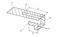
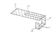
以下、添付の図面を参照しながら本発明の構成及び作用について詳細に説明する。図1は本発明による無線LANアンテナの一実施の形態を表す斜視図である。図1によると、本発明による無線LANアンテナは、所定の面積を有しながらアンテナの送受信周波数帯域を決定する放射電極(31)と、前記放射電極(31)を給電点(FP)から並列連結された2個の電流経路を有するよう区分するスロット(32)と、一端が前記放射電極(31)の所定部分に連結されて、任意の位置に電流が印加される給電点(FP)が形成される給電電極(33)と、前記給電電極(33)の他側端部に連結されて、前記放射電極(31)と所定の間隔を有する1つ以上のオープンスタブを有する整合電極(34)とで成る。 Hereinafter, the configuration and operation of the present invention will be described in detail with reference to the accompanying drawings. FIG. 1 is a perspective view illustrating a wireless LAN antenna according to an embodiment of the present invention. Referring to FIG. 1, a wireless LAN antenna according to the present invention has a radiation electrode (31) having a predetermined area and determining a transmission / reception frequency band of the antenna, and the radiation electrode (31) is connected in parallel from a feeding point (FP). A slot (32) for dividing the current into two current paths, and one end connected to a predetermined portion of the radiation electrode (31) to form a feed point (FP) to which a current is applied to an arbitrary position. A power supply electrode (33), and a matching electrode (34) connected to the other end of the power supply electrode (33) and having one or more open stubs having a predetermined distance from the radiation electrode (31). And
前記のような構造のアンテナは、誘電体セラミックあるいはポリマーから製造された所定の厚さを有する誘電体ブロックの各面に印刷して具現することもでき、またはプレス(press)により形成された後、所定の支持部材(例えば、プラスチックやポリマーから成り印刷回路基板上に固定される)により図1の形状を維持するよう支持させることもできる。 The antenna having the above structure can be embodied by printing on each surface of a dielectric block having a predetermined thickness made of dielectric ceramic or polymer, or after being formed by pressing. 1 may be supported by a predetermined supporting member (for example, made of plastic or polymer and fixed on the printed circuit board).
前記のように、本発明のアンテナはその具現方法に関係無く、前記放射電極(31)、スロット(32)、給電電極(33)、及び整合電極(34)の面積と距離、そして高さにより特性が左右される。同じく、前記放射電極(31)と給電電極(33)と整合電極(34)は、ペースト状のAg、Cuあるいは他の導電性物質をスクリーンプリンティングなどの方法により誘電体ブロックの表面に印刷後熱処理して形成するか、メッキなどの方法により形成することができ、また、板金形態のAg、Cuあるいは他の導電性電極を図3の形態に切り取り前記誘電体ブロックの表面に付着するか、印刷回路基板上に位置する支持部材でその形状を支持するよう具現することができる。 As described above, the antenna according to the present invention is not limited to the method of realizing the antenna, but has the area, the distance, and the height of the radiation electrode (31), the slot (32), the feeding electrode (33), and the matching electrode (34). Characteristics are affected. Similarly, the radiation electrode (31), the power supply electrode (33), and the matching electrode (34) are formed by printing a paste of Ag, Cu, or another conductive material on the surface of the dielectric block by a method such as screen printing. It can be formed by a method such as plating or the like, and a sheet metal form of Ag, Cu or another conductive electrode is cut into the form of FIG. 3 and attached to the surface of the dielectric block or printed. The shape may be embodied to be supported by a support member located on the circuit board.
異なった方法として、前記アンテナは前述した支持体を使用せず、前記電極ら(31、33、34)を印刷回路基板(Printed Circuit Board)上に直接形成することもできる。そして、前記スロット(32)は、給電点(FP)から入力された電流が流れる並列連結された2個以上の経路を放射電極(31)上に形成するもので、各放射領域の電気的長さに応じて相異する共振周波数が生じるようにする。従って、前記スロット(32)は、該当アンテナに要求される周波数帯域が1つの場合は必要無く、該当アンテナに要求される周波数帯域が2つ以上であれば、それに応じて多数個形成することもできる。 Alternatively, the antenna does not use the support described above, and the electrodes (31, 33, 34) can be formed directly on a printed circuit board (Printed Circuit Board). The slot (32) forms two or more paths connected in parallel on the radiation electrode (31) through which the current input from the feeding point (FP) flows, and the electrical length of each radiation area. A different resonance frequency is generated accordingly. Therefore, the slot (32) is not necessary when only one frequency band is required for the corresponding antenna, and if the frequency band required for the corresponding antenna is two or more, a large number of slots may be formed accordingly. it can.
図1の実施の形態は2.4GHzと5GHzのデュアルバンドにおいて送受信可能な無線LANアンテナを表すもので、1つのスロット(32)が形成され、前記スロット(32)により区分された放射電極(31)の2つの領域の電気的長さにより2つの帯域で共振が起こるもので、同面積の放射電極(31)があるとすれば、前記スロット(32)の長さ(D1)に応じて共振帯域が異なってくる。即ち、スロット(32)の長さ(D1)が長くなるとそれだけ電流経路が長くなり全体として共振周波数帯域が低くなり、逆にスロット(32)の長さ(D1)が短くなると電流経路が短くなり全体として共振周波数帯域が高くなる。即ち、スロット(D1)の長さ調整により、低周波数帯域と高周波数帯域両方での共振周波数を同時に調整できるのである。 The embodiment of FIG. 1 shows a wireless LAN antenna capable of transmitting and receiving signals in dual bands of 2.4 GHz and 5 GHz. One slot (32) is formed, and the radiation electrode (31) is divided by the slot (32). ), Resonance occurs in two bands due to the electrical length of the two regions. If there is a radiation electrode (31) having the same area, resonance occurs according to the length (D1) of the slot (32). The band will be different. That is, the longer the length (D1) of the slot (32), the longer the current path and the overall resonance frequency band becomes lower. Conversely, the shorter the length (D1) of the slot (32), the shorter the current path. As a whole, the resonance frequency band increases. That is, the resonance frequency in both the low frequency band and the high frequency band can be adjusted simultaneously by adjusting the length of the slot (D1).
前記放射電極(31)及びスロット(32)の形状は図1の形状に限定されず、一般に周知の如何なる形態でもよい。そして、前記整合電極(34)は「┐」(アングル、山形鋼)形態に形成され、一端は給電電極(33)を介して放射電極(31)と連結され、他端にはオープンスタブが形成され、アンテナのインピーダンスマッチング(インピーダンス整合)を調節する手段として前記オープンスタブの長さ(D2)に応じてアンテナのインピーダンスが調節される。 The shape of the radiation electrode (31) and the slot (32) is not limited to the shape shown in FIG. 1, but may be any generally known form. The matching electrode (34) is formed in the shape of "┐" (angle, angle steel), one end is connected to the radiation electrode (31) through the feeding electrode (33), and the other end is formed with an open stub. Then, as a means for adjusting the impedance matching (impedance matching) of the antenna, the impedance of the antenna is adjusted according to the length (D2) of the open stub.
具体的には、前記オープンスタブの長さ(D2)を長くすると、該当アンテナのインピーダンスサークルが大きくなりアンテナのインピーダンスが低くなり、逆にオープンスタブの長さ(D2)を短くすると、アンテナのインピーダンスが高くなり、前記整合電極(34)によりアンテナインピーダンスマッチングが可能になる。さらに、前記スロット(32)の長さ(D1)と整合電極(34)のオープンスタブ長さ(D2)とを共に調整することにより、アンテナの周波数特性及び帯域特性を共に調節できるようになる。 Specifically, when the length (D2) of the open stub is increased, the impedance circle of the corresponding antenna is increased and the impedance of the antenna is reduced. Conversely, when the length (D2) of the open stub is reduced, the impedance of the antenna is reduced. And the matching electrode (34) enables antenna impedance matching. Further, by adjusting both the length (D1) of the slot (32) and the length (D2) of the open stub of the matching electrode (34), both the frequency characteristics and the band characteristics of the antenna can be adjusted.
図1の実施の形態は本発明による無線LANアンテナの基本的な構成例を表すもので、前記構成においてスロット(32)と整合電極(34)のオープンスタブの数及び形態を変更でき、そうして最適のアンテナ設計値が得られる。例えば、図5は「┐」(アングル、山形鋼)形態のオープンスタブから突出した「−」部分を除去した本発明の無線LANアンテナにおける変形例を表すもので、整合電極(34’)が棒形状となり、この際インピーダンスマッチング(インピーダンス整合)は前記整合電極(34’)の長さ(即ち、高さ)調整により行われる。 The embodiment of FIG. 1 shows a basic configuration example of a wireless LAN antenna according to the present invention. In the above configuration, the number and configuration of the open stubs of the slot (32) and the matching electrode (34) can be changed. And an optimum antenna design value is obtained. For example, FIG. 5 shows a modification of the wireless LAN antenna of the present invention in which a “−” portion protruding from an open stub in the form of “┐” (angle, angle iron) is removed, and a matching electrode (34 ′) is a rod. At this time, impedance matching (impedance matching) is performed by adjusting the length (that is, height) of the matching electrode (34 ').
本発明のさらに他の変形例として、図6は複数のオープンスタブを有する無線LANアンテナを表すものである。図6に表すように、本発明の無線LANアンテナは給電電極(33)の他端に並列連結された2個の整合電極(34、35)をさらに具備することができる。この際、インピーダンスは前記2個の整合電極(34、35)のオープンスタブ長さの和に依存することになる。前記整合電極(34、35)の数は必要に応じてさらに増加させられる。以上のような整合電極(34、35)の変形は必要に応じて行われる。 FIG. 6 shows a wireless LAN antenna having a plurality of open stubs as still another modification of the present invention. As shown in FIG. 6, the wireless LAN antenna according to the present invention may further include two matching electrodes (34, 35) connected in parallel to the other end of the feeding electrode (33). At this time, the impedance depends on the sum of the open stub lengths of the two matching electrodes (34, 35). The number of the matching electrodes (34, 35) is further increased as needed. The deformation of the matching electrodes (34, 35) as described above is performed as needed.
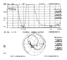
図2は図1のように2.4GHz及び5GHzの無線LAN用デュアルバンドアンテナを具現し、そのVSWRを測定したもので、この際アンテナのサイズは図10において測定した従来のアンテナと同じくした。 FIG. 2 illustrates a dual band antenna for wireless LAN of 2.4 GHz and 5 GHz as shown in FIG. 1 and its VSWR is measured. At this time, the size of the antenna is the same as the conventional antenna measured in FIG.
図10の従来の測定値と比較して図2の測定結果を見ると、従来のアンテナはマーカーP1とP2間の2.4〜2.484GHz帯域において高いVSWRを表すが、本発明のアンテナはマーカーP1とP2間の2.4〜2.484GHz帯域より広い帯域において2以下の定在波比を表す。 Referring to the measurement result of FIG. 2 in comparison with the conventional measurement value of FIG. 10, the conventional antenna shows a high VSWR in the 2.4 to 2.484 GHz band between the markers P1 and P2, but the antenna of the present invention does not A standing wave ratio of 2 or less is shown in a band wider than the 2.4 to 2.484 GHz band between the markers P1 and P2.
一般に、アンテナはVSWR(定在波電圧比)を満足する共振周波数帯域が広いほど、セット周囲環境の変化によるアンテナの特性ずれが無く安定して高性能を実現することができる。従来の無線LANアンテナは、2.4GHz帯域においてはセット及び周辺環境によりアンテナ特性が容易に歪んでしまい要求される性能を満足できないが、本発明によるアンテナは両帯域全てにおいて広い帯域幅特性を表しセット及び周辺環境の変化に対して安定した特性を呈する利点がある。 In general, the wider the resonance frequency band that satisfies the VSWR (standing-wave voltage ratio), the more stable the antenna performance can be realized without deviation of the antenna characteristics due to a change in the environment around the set. In the conventional wireless LAN antenna, the antenna characteristics are easily distorted due to the set and surrounding environment in the 2.4 GHz band, and the required performance cannot be satisfied. However, the antenna according to the present invention exhibits a wide bandwidth characteristic in both bands. There is an advantage of exhibiting stable characteristics against changes in the set and the surrounding environment.
さらに、本発明によるアンテナは5GHz帯域(マーカーP3〜マーカーP4間の帯域)においても従来のアンテナより低い定在波比を表し、このことから本発明によるデュアルバンドの無線LANアンテナは2.4GHz帯域ばかりでなく5GHz帯域までも全て良好な信号特性を呈する。 Further, the antenna according to the present invention exhibits a lower standing wave ratio than the conventional antenna even in the 5 GHz band (the band between the markers P3 and P4). Therefore, the dual-band wireless LAN antenna according to the present invention uses the 2.4 GHz band. Not only that, it also exhibits good signal characteristics up to the 5 GHz band.
そして、本発明による無線LANアンテナは、前述した整合電極(34)のオープンスタブの長さやスロット(32)の長さを調節せずに、給電電極(33)上に実際電流が入力される、即ち外部回路と接する給電点(FP)の位置を変更することによりアンテナマッチングを成すことができる。 In the wireless LAN antenna according to the present invention, an actual current is input to the feeding electrode (33) without adjusting the length of the open stub or the length of the slot (32) of the matching electrode (34). That is, antenna matching can be achieved by changing the position of the feeding point (FP) in contact with the external circuit.
図3(A)と(B)は、図1の無線LANアンテナにおいて給電点(FP)の位置を変更した例を表すものである。先ず、図3(A)は、図1の無線LANアンテナにおいて給電点(FP)を放射電極(31)側に偏るよう位置させたもので、この場合、相対的に整合電極(34)のオープンスタブの長さが長くなる効果が得られる。即ち、給電点(FP)が放射電極(31)側へ偏った分だけ整合電極(34)のオープンスタブ長さが長くなり、その結果アンテナのインピーダンスが低くなる方(即ち、インピーダンスサークルが大きくなる方向)にインピーダンスを調節できるようになる。さらに、放射電極(31)の側面から見ると給電点(FP)が放射電極(31)側に偏ることにより、相対的に電流経路が短くなる効果を奏し、従って共振帯域の中心周波数が高い方に移動する。 FIGS. 3A and 3B show an example in which the position of the feeding point (FP) is changed in the wireless LAN antenna of FIG. First, FIG. 3A shows the wireless LAN antenna of FIG. 1 in which the feeding point (FP) is positioned so as to be biased toward the radiation electrode (31). In this case, the matching electrode (34) is relatively opened. The effect of increasing the length of the stub is obtained. That is, the length of the open stub of the matching electrode (34) is increased by an amount corresponding to the deviation of the feeding point (FP) toward the radiation electrode (31), and as a result, the impedance of the antenna decreases (that is, the impedance circle increases). Direction) to adjust the impedance. Furthermore, when viewed from the side surface of the radiation electrode (31), the feeding point (FP) is biased toward the radiation electrode (31), which has the effect of shortening the current path relatively. Therefore, the center frequency of the resonance band is higher. Go to
次に、図3(B)は図1の無線LANアンテナにおいて給電点(FP)を整合電極(34)側に偏るよう形成した場合で、今度は逆に、電流経路は長くなりオープンスタブの長さは短くなり、アンテナのインピーダンスが高くなる方向に調節され、共振帯域の中心周波数は低い周波数方向へ移動する。 Next, FIG. 3B shows a case in which the feeding point (FP) is formed so as to be biased toward the matching electrode (34) in the wireless LAN antenna of FIG. 1. On the contrary, the current path becomes longer and the length of the open stub becomes longer. And the antenna frequency is adjusted to increase the impedance of the antenna, and the center frequency of the resonance band moves in the lower frequency direction.
従って、本発明による無線LANアンテナは、給電点(FP)の位置変更だけでもアンテナのインピーダンスと中心周波数を共に変化させ、セット別に各々最適のアンテナ具現を容易にする。さらに、本発明による無線LANアンテナはモノポールタイプアンテナから逆F型アンテナに変更することができる。 Therefore, the wireless LAN antenna according to the present invention changes both the impedance and the center frequency of the antenna only by changing the position of the feeding point (FP), and facilitates the implementation of the optimum antenna for each set. Further, the wireless LAN antenna according to the present invention can be changed from a monopole type antenna to an inverted F type antenna.
先に説明したように、逆F型アンテナは一側から放射電極へ電流を与えると同時に放射電極を接地させる。従って、給電点と接地点とが同時に表れるが、図4のように、本発明による無線LANアンテナは給電点(FP)を有する給電電極(33)の所定の点を接地させることにより、逆F型アンテナに変形させられる。前記給電電極(33)上において接地された部分を接地点(SP)といい、前記給電点(FP)と接地点(SP)との間隔及び位置を調整することにより、セットにおいて印刷回路基板のグラウンド条件が大幅に異なってもアンテナのインピーダンスマッチング(インピーダンス整合)及びこのうち共振周波数の変更を容易にすることができる。以上のような本発明の無線LANアンテナは、垂直偏波用と水平偏波用とに2個のアンテナを用するダイバーシチアンテナの具現にとりわけ有利である。 As described above, the inverted-F antenna applies a current to the radiation electrode from one side and grounds the radiation electrode at the same time. Therefore, the feeding point and the ground point appear at the same time, but as shown in FIG. 4, the wireless LAN antenna according to the present invention connects the predetermined point of the feeding electrode (33) having the feeding point (FP) to the ground so that the reverse F Shaped antenna. The portion grounded on the power supply electrode (33) is referred to as a ground point (SP). By adjusting the distance and position between the power supply point (FP) and the ground point (SP), the set of the printed circuit board in the set is adjusted. Even if the ground conditions are significantly different, it is possible to easily change the impedance matching (impedance matching) of the antenna and change the resonance frequency. The wireless LAN antenna of the present invention as described above is particularly advantageous for implementing a diversity antenna using two antennas for vertical polarization and horizontal polarization.
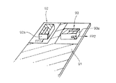
図7及び図8は無線LANカードにおいて本発明のアンテナを用いてダイバーシチアンテナを具現する実施の形態を表すものである。先ず、図7は本発明による無線LANアンテナをチップアンテナタイプに製造して用いたもので、無線LANカードの印刷回路基板(91)上に、縦方向に第1アンテナ(92)を付着後、前記第1アンテナ(92)に直交する方向に第2アンテナ(93)を付着する。この際、第1アンテナ(92)との干渉により第2アンテナ(93)の特性がセット毎に異なることがある。このため、第2アンテナ(93)を印刷回路基板(91)上にハンダ付けする前に、誘電体ブロック(93a)の下面に形成された給電電極上の給電点(FP2)(即ち、印刷回路基板のパターンとハンダ付けされる点)の位置を調整しながら最適の特性を呈するようアンテナ特性を調整することができる。同じく、第1アンテナ(92)も給電点(FP1)の位置を調整してアンテナ特性を調整することができる。 7 and 8 show an embodiment in which a diversity antenna is implemented using the antenna of the present invention in a wireless LAN card. First, FIG. 7 shows a case where a wireless LAN antenna according to the present invention is manufactured and used as a chip antenna type, and a first antenna (92) is attached in a vertical direction on a printed circuit board (91) of a wireless LAN card. A second antenna (93) is attached in a direction orthogonal to the first antenna (92). At this time, the characteristics of the second antenna (93) may be different for each set due to interference with the first antenna (92). Therefore, before soldering the second antenna (93) on the printed circuit board (91), the feeding point (FP2) on the feeding electrode formed on the lower surface of the dielectric block (93a) (that is, the printed circuit) The antenna characteristics can be adjusted so as to exhibit the optimum characteristics while adjusting the position of the point of soldering with the pattern of the substrate. Similarly, the antenna characteristics of the first antenna (92) can be adjusted by adjusting the position of the feeding point (FP1).
次に、図8は本発明による無線LANアンテナで具現した異なる形態のダイバーシチアンテナで、無線LAN信号を処理する複数の回路及び素子が装着される印刷回路基板(101)上の所定位置にポリマーまたはプラスチック材質から成るアンテナ支持部材(102)を形成し、前記アンテナ支持部材(102)により本発明の第1、第2アンテナ(103、104)が相互に垂直に配置されるよう支持する。 Next, FIG. 8 shows a diversity antenna of a different form embodied by the wireless LAN antenna according to the present invention, wherein a polymer or a polymer is placed at a predetermined position on a printed circuit board (101) on which a plurality of circuits and elements for processing a wireless LAN signal are mounted. An antenna support member (102) made of a plastic material is formed, and the first and second antennas (103, 104) of the present invention are supported by the antenna support member (102) so as to be arranged perpendicular to each other.
この際、第1、第2アンテナ(103、104)の放射電極はアンテナ支持部材(102)の上部面に位置し、第1、第2アンテナ(103、104)の給電電極は印刷回路基板(101)に位置して、その電極上の所定の点が信号パターン及び/または接地パターンにハンダ付けされる。 At this time, the radiation electrodes of the first and second antennas (103, 104) are located on the upper surface of the antenna support member (102), and the feed electrodes of the first and second antennas (103, 104) are printed circuit boards ( At 101), a predetermined point on the electrode is soldered to the signal and / or ground pattern.
前記アンテナ支持部材(102)は第1、第2アンテナ(103、104)の放射電極が印刷回路基板(101)から所定の高さで位置するよう支持するもので、特別な形態に制限されはしない。この際、第1、第2アンテナ(103、104)は、金属板をプレスにより先述した放射電極(31)、スロット(32)、給電電極(33)、整合電極(34)を有するよう形成して成ったものである。 The antenna support member (102) supports the radiation electrodes of the first and second antennas (103, 104) at a predetermined height from the printed circuit board (101), and is not limited to a special form. do not do. At this time, the first and second antennas (103, 104) are formed by pressing a metal plate to have the above-mentioned radiation electrode (31), slot (32), feeding electrode (33), and matching electrode (34). It is made up of
そして、図8のダイバーシチアンテナも、先に図7で説明したように、第1、第2アンテナ(103、104)の給電点を変更しインピーダンスを調節することにより第1、第2アンテナ(103、104)間の干渉による影響を最小化することができる。 The diversity antenna of FIG. 8 also changes the feed points of the first and second antennas (103, 104) and adjusts the impedance as described with reference to FIG. , 104) can be minimized.
30 誘電体ブロック
31 放射電極
32 スロット
33 給電電極
34 整合電極
FP 給電点(feeding point)
SP 接地点(short point)
Reference Signs List 30
SP ground point (short point)
Claims (12)
1つ以上のオープンスタブを有する整合電極と、
一端は前記放射電極に連結されて他端は前記整合電極に連結され、電極上の任意の位置に電流が印加される給電点を有する給電電極と、
を有することを特徴とする無線LANアンテナ。 A radiation electrode that determines the transmission and reception frequency band of the antenna while having a predetermined area,
A matching electrode having one or more open stubs;
One end is connected to the radiation electrode, the other end is connected to the matching electrode, and a feeding electrode having a feeding point to which a current is applied to an arbitrary position on the electrode;
A wireless LAN antenna comprising:
1つ以上のオープンスタブを有する整合電極と、
一端は前記放射電極に連結されて他端は前記整合電極に連結され、電極上の任意の位置に電流が印加される給電点とグラウンドに連結される接地点とが具備される給電電極と、
を有することを特徴とする逆Fタイプ無線LANアンテナ。 A radiation electrode that determines the transmission and reception frequency band of the antenna while having a predetermined area,
A matching electrode having one or more open stubs;
One end is connected to the radiation electrode, the other end is connected to the matching electrode, and a power supply electrode including a power supply point to which a current is applied to an arbitrary position on the electrode and a ground point connected to the ground;
An inverted-F type wireless LAN antenna, comprising:
所定の面積を有するよう前記誘電体ブロックの上面に形成されながらアンテナの送受信周波数帯域を決定する放射電極と、
前記誘電体ブロックの前面に前記放射電極とは直に接触しないよう「┐」(アングル、山形鋼)形状に形成された整合電極と、
前記誘電体ブロックの後面及び下面にかけて形成され、一端は前記放射電極に他端は前記整合電極に連結され、下面に形成された電極上に給電点が形成される給電電極と、
を有することを特徴とする無線LANアンテナ。 A rectangular parallelepiped dielectric block;
A radiation electrode that determines a transmission / reception frequency band of the antenna while being formed on the upper surface of the dielectric block so as to have a predetermined area,
A matching electrode formed in a “┐” (angle, angle steel) shape so as not to directly contact the radiation electrode on the front surface of the dielectric block;
A power supply electrode formed over the rear surface and the lower surface of the dielectric block, one end connected to the radiation electrode and the other end to the matching electrode, and a power supply point formed on an electrode formed on the lower surface;
A wireless LAN antenna comprising:
直方体形状の誘電体ブロックの上面に所定の面積を有しながらアンテナの送受信周波数帯域を決定する放射電極が印刷され、前記誘電体ブロックの前面に前記放射電極とは直に接触しないようオープンスタブの整合電極が印刷され、前記誘電体ブロックの後面及び下面にかけて一端は前記放射電極に他端は前記整合電極に連結される給電電極が印刷されて成り、相互垂直に配置されるよう前記印刷回路基板上に装着される第1、第2アンテナとを含み、
前記第1、第2アンテナにおいて前記印刷回路基板への装着時に前記給電電極上の給電点を調整することにより、インピーダンスマッチングを調整できることを特徴とする無線LANカード。 A printed circuit board on which a plurality of semiconductor chips and elements are mounted for processing wireless LAN signals;
A radiating electrode that determines the transmitting and receiving frequency band of the antenna is printed on the upper surface of the rectangular parallelepiped dielectric block while having a predetermined area, and an open stub is formed on the front surface of the dielectric block so as not to directly contact the radiating electrode. The printed circuit board is printed with a matching electrode, and has a radiation electrode on one end and a feeding electrode connected to the matching electrode on the other end printed on the rear surface and the lower surface of the dielectric block. First and second antennas mounted thereon,
A wireless LAN card wherein impedance matching can be adjusted by adjusting a feed point on the feed electrode when the first and second antennas are mounted on the printed circuit board.
前記印刷回路基板の所定の位置に当該基板から所定の高さで位置するよう固定されるアンテナ支持部材と、
所定の面積を有しながらアンテナの送受信周波数帯域を決定する放射電極と、1つ以上のオープンスタブを有する整合電極と、一端は前記放射電極に連結されて他端は前記整合電極に連結され電極上の任意の位置に電流が印加される給電点を有する給電電極とで成り、各々の放射電極が前記アンテナ支持部材により相互垂直するよう支持され、前記給電電極は前記印刷回路基板の所定の位置にハンダ付けされる第1、第2アンテナとを含み、
前記第1、第2アンテナにおいて前記印刷回路基板への装着時に前記給電電極上の給電点を調整することにより、インピーダンスマッチングを調整できることを特徴とする無線LANカード。 A printed circuit board on which a plurality of semiconductor chips and elements are mounted for processing wireless LAN signals;
An antenna support member fixed to a predetermined position of the printed circuit board at a predetermined height from the substrate,
A radiating electrode having a predetermined area and determining a transmission / reception frequency band of the antenna, a matching electrode having one or more open stubs, and one end connected to the radiating electrode and the other end connected to the matching electrode. And a feed electrode having a feed point to which a current is applied at an arbitrary position above, and each radiation electrode is supported by the antenna support member so as to be perpendicular to each other, and the feed electrode is located at a predetermined position on the printed circuit board. First and second antennas soldered to
A wireless LAN card wherein impedance matching can be adjusted by adjusting a feed point on the feed electrode when the first and second antennas are mounted on the printed circuit board.
Applications Claiming Priority (2)
| Application Number | Priority Date | Filing Date | Title |
|---|---|---|---|
| KR20020080250 | 2002-12-16 | ||
| KR1020030041171A KR100541080B1 (en) | 2002-12-16 | 2003-06-24 | Antenna for wireless-lan and wireless lan card with the same |
Publications (1)
| Publication Number | Publication Date |
|---|---|
| JP2004201281A true JP2004201281A (en) | 2004-07-15 |
Family
ID=32599372
Family Applications (1)
| Application Number | Title | Priority Date | Filing Date |
|---|---|---|---|
| JP2003350451A Pending JP2004201281A (en) | 2002-12-16 | 2003-10-09 | Wireless lan antenna and wireless lan card provided with the same |
Country Status (5)
| Country | Link |
|---|---|
| US (1) | US6965346B2 (en) |
| JP (1) | JP2004201281A (en) |
| CN (1) | CN1314165C (en) |
| DE (1) | DE10347722A1 (en) |
| TW (1) | TWI256179B (en) |
Cited By (11)
| Publication number | Priority date | Publication date | Assignee | Title |
|---|---|---|---|---|
| JP2007184883A (en) * | 2005-12-06 | 2007-07-19 | Furukawa Electric Co Ltd:The | Multiple frequency antenna |
| JP2007266669A (en) * | 2006-03-27 | 2007-10-11 | Fujitsu Ltd | Antenna and radio device |
| KR100849810B1 (en) | 2006-02-10 | 2008-07-31 | 가시오 히타치 모바일 커뮤니케이션즈 컴퍼니 리미티드 | Antenna apparatus |
| US7538732B2 (en) | 2005-01-05 | 2009-05-26 | Murata Manufacturing Co., Ltd. | Antenna structure and radio communication apparatus including the same |
| WO2009113143A1 (en) * | 2008-03-11 | 2009-09-17 | パナソニック株式会社 | Anntena element |
| KR100964652B1 (en) * | 2007-05-03 | 2010-06-22 | 주식회사 이엠따블유 | Multi-band antenna and wireless communication device including the same |
| JP2010199876A (en) * | 2009-02-24 | 2010-09-09 | Fujikura Ltd | Antenna and wireless communication apparatus |
| JP2010206795A (en) * | 2009-02-27 | 2010-09-16 | Thomson Licensing | Compact antenna system with diversity order of 2 |
| KR101561945B1 (en) | 2009-07-13 | 2015-10-21 | 삼성전자 주식회사 | Antenna apparatus and mobile device having the same |
| JP2018129769A (en) * | 2017-02-10 | 2018-08-16 | 株式会社フジクラ | Antenna device |
| JP7123641B2 (en) | 2018-06-07 | 2022-08-23 | 株式会社東芝 | chip antenna |
Families Citing this family (31)
| Publication number | Priority date | Publication date | Assignee | Title |
|---|---|---|---|---|
| KR100548057B1 (en) * | 2005-06-03 | 2006-02-01 | (주)파트론 | Surface mount technology antenna apparatus with trio land structure |
| WO2006134701A1 (en) * | 2005-06-17 | 2006-12-21 | Murata Manufacturing Co., Ltd. | Antenna device and wireless communication device |
| GB2434697B (en) * | 2006-01-31 | 2008-07-02 | Motorola Inc | RF communication device and method of operation of the device |
| US7548208B2 (en) * | 2006-02-24 | 2009-06-16 | Palm, Inc. | Internal diversity antenna architecture |
| TWI313526B (en) * | 2006-07-14 | 2009-08-11 | Hon Hai Prec Ind Co Ltd | Antenna device |
| TW200810231A (en) * | 2006-08-11 | 2008-02-16 | Hon Hai Prec Ind Co Ltd | Antenna device |
| JP2008124617A (en) | 2006-11-09 | 2008-05-29 | Tyco Electronics Amp Kk | Antenna |
| TWI412176B (en) * | 2006-12-04 | 2013-10-11 | Wistron Neweb Corp | Three-dimensional multi-frequency antenna |
| US7903032B2 (en) * | 2007-04-05 | 2011-03-08 | Sony Ericsson Mobile Communications Ab | Antenna for a communication terminal |
| EP2028718B1 (en) * | 2007-08-23 | 2014-01-15 | BlackBerry Limited | Multi-band antenna, and associated methodology, for a radio communication device |
| KR100910526B1 (en) * | 2007-11-20 | 2009-07-31 | 삼성전기주식회사 | Antenna and mobile communication device using the same |
| JP4849172B2 (en) * | 2008-01-29 | 2012-01-11 | 株式会社村田製作所 | Antenna structure and wireless communication apparatus including the same |
| WO2010008269A1 (en) * | 2008-07-14 | 2010-01-21 | Laird Technologies, Inc. | Multi-band antenna assemblies for use with wireless application devices |
| TWI491111B (en) * | 2008-12-12 | 2015-07-01 | Chi Mei Comm Systems Inc | Monopole antenna |
| EP2323217B1 (en) * | 2009-11-13 | 2014-04-30 | BlackBerry Limited | Antenna for multi mode mimo communication in handheld devices |
| US8754814B2 (en) * | 2009-11-13 | 2014-06-17 | Blackberry Limited | Antenna for multi mode MIMO communication in handheld devices |
| JP2011119949A (en) * | 2009-12-02 | 2011-06-16 | Mitsumi Electric Co Ltd | Card device |
| TWI496349B (en) * | 2010-12-23 | 2015-08-11 | Hon Hai Prec Ind Co Ltd | Antenna |
| CN104332719A (en) * | 2013-07-22 | 2015-02-04 | 联想(北京)有限公司 | Antenna device, electronic equipment and method for setting the antenna device |
| CN105409058B (en) * | 2014-04-28 | 2018-08-14 | 华为终端(东莞)有限公司 | A kind of antenna assembly and terminal |
| USD754108S1 (en) * | 2014-10-29 | 2016-04-19 | Airgain, Inc. | Antenna |
| EP3200280B1 (en) * | 2014-10-31 | 2021-08-25 | Huawei Technologies Co., Ltd. | Wireless mobile device |
| CN106299638A (en) * | 2016-05-20 | 2017-01-04 | 北京小鸟听听科技有限公司 | A kind of for surface-pasted antenna and design and production method thereof |
| NL2019365B1 (en) | 2017-07-28 | 2019-02-18 | The Antenna Company International N V | Component for a dual band antenna, a dual band antenna comprising said component, and a dual band antenna system. |
| USD856313S1 (en) | 2017-04-25 | 2019-08-13 | The Antenna Company International N.V. | Dual port antenna |
| US10985455B2 (en) | 2017-04-25 | 2021-04-20 | The Antenna Company International N.V. | EBG structure, EBG component, and antenna device |
| USD883962S1 (en) | 2017-04-25 | 2020-05-12 | The Antenna Company International N.V. | Dual port antenna assembly |
| CN107482306A (en) * | 2017-07-06 | 2017-12-15 | 安徽省广播电视科研所 | Back feed type film-type DTV isotropic receiving antenna |
| CN109309283A (en) | 2017-07-27 | 2019-02-05 | 国基电子(上海)有限公司 | Antenna assembly |
| TWI658646B (en) * | 2017-07-27 | 2019-05-01 | 鴻海精密工業股份有限公司 | Antenna device |
| TWI747538B (en) * | 2020-10-05 | 2021-11-21 | 廣達電腦股份有限公司 | Antenna system |
Family Cites Families (11)
| Publication number | Priority date | Publication date | Assignee | Title |
|---|---|---|---|---|
| US5696517A (en) | 1995-09-28 | 1997-12-09 | Murata Manufacturing Co., Ltd. | Surface mounting antenna and communication apparatus using the same |
| FI105061B (en) | 1998-10-30 | 2000-05-31 | Lk Products Oy | Planar antenna with two resonant frequencies |
| US6768460B2 (en) * | 2000-03-29 | 2004-07-27 | Matsushita Electric Industrial Co., Ltd. | Diversity wireless device and wireless terminal unit |
| JP2002028803A (en) | 2000-05-10 | 2002-01-29 | Mitsubishi Materials Corp | Throw-away cutting tip made of surface coated tungsten carbide-base cemented carbide having good interlayer adhesiveness of hard coat layer |
| DE10049845A1 (en) | 2000-10-09 | 2002-04-11 | Philips Corp Intellectual Pty | Multiband microwave aerial with substrate with one or more conductive track structures |
| US6448933B1 (en) | 2001-04-11 | 2002-09-10 | Tyco Electronics Logisitics Ag | Polarization and spatial diversity antenna assembly for wireless communication devices |
| TW538559B (en) * | 2001-07-18 | 2003-06-21 | Matsushita Electric Ind Co Ltd | Antenna device and mobile communications apparatus including the device |
| US6717548B2 (en) * | 2001-08-02 | 2004-04-06 | Auden Techno Corp. | Dual- or multi-frequency planar inverted F-antenna |
| TW512558B (en) * | 2002-01-16 | 2002-12-01 | Accton Technology Corp | Surface-mountable dual-band monopole antenna for WLAN application |
| KR100483043B1 (en) * | 2002-04-11 | 2005-04-18 | 삼성전기주식회사 | Multi band built-in antenna |
| US20030206136A1 (en) * | 2002-05-02 | 2003-11-06 | Po-Chao Chen | Inverted-F antenna |
-
2003
- 2003-09-30 US US10/673,265 patent/US6965346B2/en not_active Expired - Fee Related
- 2003-10-07 TW TW092127869A patent/TWI256179B/en not_active IP Right Cessation
- 2003-10-09 JP JP2003350451A patent/JP2004201281A/en active Pending
- 2003-10-14 DE DE10347722A patent/DE10347722A1/en not_active Ceased
- 2003-10-15 CN CNB2003101012510A patent/CN1314165C/en not_active Expired - Fee Related
Cited By (17)
| Publication number | Priority date | Publication date | Assignee | Title |
|---|---|---|---|---|
| US7538732B2 (en) | 2005-01-05 | 2009-05-26 | Murata Manufacturing Co., Ltd. | Antenna structure and radio communication apparatus including the same |
| JP2007184883A (en) * | 2005-12-06 | 2007-07-19 | Furukawa Electric Co Ltd:The | Multiple frequency antenna |
| JP4676340B2 (en) * | 2005-12-06 | 2011-04-27 | 古河電気工業株式会社 | Multi-frequency antenna |
| KR100849810B1 (en) | 2006-02-10 | 2008-07-31 | 가시오 히타치 모바일 커뮤니케이션즈 컴퍼니 리미티드 | Antenna apparatus |
| US7554495B2 (en) | 2006-02-10 | 2009-06-30 | Casio Hitachi Mobile Communications Co., Ltd. | Antenna apparatus |
| JP2007266669A (en) * | 2006-03-27 | 2007-10-11 | Fujitsu Ltd | Antenna and radio device |
| JP4522386B2 (en) * | 2006-03-27 | 2010-08-11 | 富士通株式会社 | Antenna and radio apparatus |
| JP2010526471A (en) * | 2007-05-03 | 2010-07-29 | イーエムダブリュ カンパニー リミテッド | Multi-band antenna and wireless communication apparatus including the same |
| KR100964652B1 (en) * | 2007-05-03 | 2010-06-22 | 주식회사 이엠따블유 | Multi-band antenna and wireless communication device including the same |
| JP2009218917A (en) * | 2008-03-11 | 2009-09-24 | Panasonic Corp | Antenna element |
| CN101971421A (en) * | 2008-03-11 | 2011-02-09 | 松下电器产业株式会社 | Antenna element |
| WO2009113143A1 (en) * | 2008-03-11 | 2009-09-17 | パナソニック株式会社 | Anntena element |
| JP2010199876A (en) * | 2009-02-24 | 2010-09-09 | Fujikura Ltd | Antenna and wireless communication apparatus |
| JP2010206795A (en) * | 2009-02-27 | 2010-09-16 | Thomson Licensing | Compact antenna system with diversity order of 2 |
| KR101561945B1 (en) | 2009-07-13 | 2015-10-21 | 삼성전자 주식회사 | Antenna apparatus and mobile device having the same |
| JP2018129769A (en) * | 2017-02-10 | 2018-08-16 | 株式会社フジクラ | Antenna device |
| JP7123641B2 (en) | 2018-06-07 | 2022-08-23 | 株式会社東芝 | chip antenna |
Also Published As
| Publication number | Publication date |
|---|---|
| US20040125030A1 (en) | 2004-07-01 |
| DE10347722A1 (en) | 2004-07-15 |
| TWI256179B (en) | 2006-06-01 |
| CN1314165C (en) | 2007-05-02 |
| US6965346B2 (en) | 2005-11-15 |
| TW200411982A (en) | 2004-07-01 |
| CN1508907A (en) | 2004-06-30 |
Similar Documents
| Publication | Publication Date | Title |
|---|---|---|
| JP2004201281A (en) | Wireless lan antenna and wireless lan card provided with the same | |
| US5828340A (en) | Wideband sub-wavelength antenna | |
| US8581785B2 (en) | Multilevel and space-filling ground-planes for miniature and multiband antennas | |
| KR100707242B1 (en) | Dielectric chip antenna | |
| US6606067B2 (en) | Apparatus for wideband directional antenna | |
| KR100265510B1 (en) | Omnidirectional dipole antenna | |
| JP2006115448A (en) | Wide-band built-in antenna | |
| US20050122267A1 (en) | Internal triple-band antenna | |
| KR20030090716A (en) | Dual band patch bowtie slot antenna structure | |
| JP2006319767A (en) | Flat antenna | |
| KR100616545B1 (en) | Multi-band laminated chip antenna using double coupling feeding | |
| JP2011528520A (en) | Antenna device | |
| US20040217910A1 (en) | Monolithic low profile omni-directional surface-mount antenna | |
| US9985349B1 (en) | Multi-band LTE antenna | |
| JPH07303005A (en) | Antenna system for vehicle | |
| JP2010087752A (en) | Multiband antenna | |
| US20100164811A1 (en) | Solid Antenna | |
| KR100541080B1 (en) | Antenna for wireless-lan and wireless lan card with the same | |
| US11811149B2 (en) | Multi-band antenna | |
| US7924233B2 (en) | Three-dimensional antenna and related wireless communication device | |
| KR100992864B1 (en) | Wideband antenna for covering both CDMA frequency band and UWB frequency band | |
| US7482980B2 (en) | Three-dimensional wideband antenna and related wireless communication device | |
| KR100862533B1 (en) | Multi band antenna | |
| JPH09232854A (en) | Small planar antenna system for mobile radio equipment | |
| CN112242605B (en) | Antenna structure |
Legal Events
| Date | Code | Title | Description |
|---|---|---|---|
| A131 | Notification of reasons for refusal |
Free format text: JAPANESE INTERMEDIATE CODE: A131 Effective date: 20060214 |
|
| A601 | Written request for extension of time |
Free format text: JAPANESE INTERMEDIATE CODE: A601 Effective date: 20060512 |
|
| A602 | Written permission of extension of time |
Free format text: JAPANESE INTERMEDIATE CODE: A602 Effective date: 20060517 |
|
| A02 | Decision of refusal |
Free format text: JAPANESE INTERMEDIATE CODE: A02 Effective date: 20060627 |