JP2004072060A - Transistor and semiconductor memory using the same, and method of driving the transistor - Google Patents
Transistor and semiconductor memory using the same, and method of driving the transistor Download PDFInfo
- Publication number
- JP2004072060A JP2004072060A JP2002322905A JP2002322905A JP2004072060A JP 2004072060 A JP2004072060 A JP 2004072060A JP 2002322905 A JP2002322905 A JP 2002322905A JP 2002322905 A JP2002322905 A JP 2002322905A JP 2004072060 A JP2004072060 A JP 2004072060A
- Authority
- JP
- Japan
- Prior art keywords
- insulating film
- source
- gate
- floating gate
- erasing
- Prior art date
- Legal status (The legal status is an assumption and is not a legal conclusion. Google has not performed a legal analysis and makes no representation as to the accuracy of the status listed.)
- Pending
Links
- 239000004065 semiconductor Substances 0.000 title claims abstract description 79
- 238000000034 method Methods 0.000 title claims description 57
- 238000007667 floating Methods 0.000 claims abstract description 262
- 239000000758 substrate Substances 0.000 claims abstract description 45
- 238000002347 injection Methods 0.000 claims description 36
- 239000007924 injection Substances 0.000 claims description 36
- 239000002344 surface layer Substances 0.000 claims description 10
- 229910021420 polycrystalline silicon Inorganic materials 0.000 abstract description 17
- 229920005591 polysilicon Polymers 0.000 abstract description 17
- 239000012535 impurity Substances 0.000 abstract description 16
- 230000015654 memory Effects 0.000 description 44
- 229910052581 Si3N4 Inorganic materials 0.000 description 34
- HQVNEWCFYHHQES-UHFFFAOYSA-N silicon nitride Chemical compound N12[Si]34N5[Si]62N3[Si]51N64 HQVNEWCFYHHQES-UHFFFAOYSA-N 0.000 description 34
- VYPSYNLAJGMNEJ-UHFFFAOYSA-N Silicium dioxide Chemical compound O=[Si]=O VYPSYNLAJGMNEJ-UHFFFAOYSA-N 0.000 description 31
- 229910052814 silicon oxide Inorganic materials 0.000 description 31
- 229910052796 boron Inorganic materials 0.000 description 26
- ZOXJGFHDIHLPTG-UHFFFAOYSA-N Boron Chemical compound [B] ZOXJGFHDIHLPTG-UHFFFAOYSA-N 0.000 description 25
- 229920002120 photoresistant polymer Polymers 0.000 description 25
- 238000005530 etching Methods 0.000 description 20
- 238000004519 manufacturing process Methods 0.000 description 18
- XUIMIQQOPSSXEZ-UHFFFAOYSA-N Silicon Chemical compound [Si] XUIMIQQOPSSXEZ-UHFFFAOYSA-N 0.000 description 17
- 229910052710 silicon Inorganic materials 0.000 description 17
- 239000010703 silicon Substances 0.000 description 17
- 230000008859 change Effects 0.000 description 15
- 238000010586 diagram Methods 0.000 description 15
- 238000005468 ion implantation Methods 0.000 description 13
- 150000002500 ions Chemical class 0.000 description 13
- 239000010410 layer Substances 0.000 description 13
- 229910052785 arsenic Inorganic materials 0.000 description 10
- RQNWIZPPADIBDY-UHFFFAOYSA-N arsenic atom Chemical compound [As] RQNWIZPPADIBDY-UHFFFAOYSA-N 0.000 description 10
- 230000006870 function Effects 0.000 description 10
- 230000001133 acceleration Effects 0.000 description 9
- 230000008901 benefit Effects 0.000 description 9
- 230000005684 electric field Effects 0.000 description 9
- 230000003647 oxidation Effects 0.000 description 9
- 238000007254 oxidation reaction Methods 0.000 description 9
- 229920006395 saturated elastomer Polymers 0.000 description 8
- 230000007423 decrease Effects 0.000 description 7
- 239000002784 hot electron Substances 0.000 description 7
- 238000002955 isolation Methods 0.000 description 7
- 239000000969 carrier Substances 0.000 description 6
- 230000003247 decreasing effect Effects 0.000 description 6
- 238000009826 distribution Methods 0.000 description 6
- 230000015556 catabolic process Effects 0.000 description 5
- 238000009825 accumulation Methods 0.000 description 4
- QVGXLLKOCUKJST-UHFFFAOYSA-N atomic oxygen Chemical compound [O] QVGXLLKOCUKJST-UHFFFAOYSA-N 0.000 description 4
- 238000005229 chemical vapour deposition Methods 0.000 description 4
- 230000002950 deficient Effects 0.000 description 4
- OAICVXFJPJFONN-UHFFFAOYSA-N Phosphorus Chemical compound [P] OAICVXFJPJFONN-UHFFFAOYSA-N 0.000 description 3
- 230000008878 coupling Effects 0.000 description 3
- 238000010168 coupling process Methods 0.000 description 3
- 238000005859 coupling reaction Methods 0.000 description 3
- 238000009792 diffusion process Methods 0.000 description 3
- 229910052698 phosphorus Inorganic materials 0.000 description 3
- 239000011574 phosphorus Substances 0.000 description 3
- -1 Metal Oxide Nitride Chemical class 0.000 description 2
- 230000007547 defect Effects 0.000 description 2
- 230000000694 effects Effects 0.000 description 2
- 238000011065 in-situ storage Methods 0.000 description 2
- 229910052743 krypton Inorganic materials 0.000 description 2
- DNNSSWSSYDEUBZ-UHFFFAOYSA-N krypton atom Chemical compound [Kr] DNNSSWSSYDEUBZ-UHFFFAOYSA-N 0.000 description 2
- 229910052751 metal Inorganic materials 0.000 description 2
- 239000002184 metal Substances 0.000 description 2
- 229910052760 oxygen Inorganic materials 0.000 description 2
- 239000001301 oxygen Substances 0.000 description 2
- 238000001020 plasma etching Methods 0.000 description 2
- 230000008569 process Effects 0.000 description 2
- 238000012545 processing Methods 0.000 description 2
- 230000009467 reduction Effects 0.000 description 2
- 229910052782 aluminium Inorganic materials 0.000 description 1
- XAGFODPZIPBFFR-UHFFFAOYSA-N aluminium Chemical compound [Al] XAGFODPZIPBFFR-UHFFFAOYSA-N 0.000 description 1
- 230000004888 barrier function Effects 0.000 description 1
- 230000015572 biosynthetic process Effects 0.000 description 1
- 238000012790 confirmation Methods 0.000 description 1
- 238000007796 conventional method Methods 0.000 description 1
- 239000013078 crystal Substances 0.000 description 1
- 230000007812 deficiency Effects 0.000 description 1
- 238000001514 detection method Methods 0.000 description 1
- 230000006866 deterioration Effects 0.000 description 1
- 230000002542 deteriorative effect Effects 0.000 description 1
- 238000011161 development Methods 0.000 description 1
- 238000005516 engineering process Methods 0.000 description 1
- 239000007943 implant Substances 0.000 description 1
- 238000009413 insulation Methods 0.000 description 1
- 239000012212 insulator Substances 0.000 description 1
- 230000010354 integration Effects 0.000 description 1
- 239000012528 membrane Substances 0.000 description 1
- 229910044991 metal oxide Inorganic materials 0.000 description 1
- 150000004767 nitrides Chemical class 0.000 description 1
- 238000000059 patterning Methods 0.000 description 1
- 238000004904 shortening Methods 0.000 description 1
- 239000007787 solid Substances 0.000 description 1
- 239000000243 solution Substances 0.000 description 1
- 238000011105 stabilization Methods 0.000 description 1
- 238000003860 storage Methods 0.000 description 1
- 230000005641 tunneling Effects 0.000 description 1
Images


Classifications
-
- H—ELECTRICITY
- H01—ELECTRIC ELEMENTS
- H01L—SEMICONDUCTOR DEVICES NOT COVERED BY CLASS H10
- H01L27/00—Devices consisting of a plurality of semiconductor or other solid-state components formed in or on a common substrate
- H01L27/02—Devices consisting of a plurality of semiconductor or other solid-state components formed in or on a common substrate including semiconductor components specially adapted for rectifying, oscillating, amplifying or switching and having potential barriers; including integrated passive circuit elements having potential barriers
- H01L27/04—Devices consisting of a plurality of semiconductor or other solid-state components formed in or on a common substrate including semiconductor components specially adapted for rectifying, oscillating, amplifying or switching and having potential barriers; including integrated passive circuit elements having potential barriers the substrate being a semiconductor body
- H01L27/10—Devices consisting of a plurality of semiconductor or other solid-state components formed in or on a common substrate including semiconductor components specially adapted for rectifying, oscillating, amplifying or switching and having potential barriers; including integrated passive circuit elements having potential barriers the substrate being a semiconductor body including a plurality of individual components in a repetitive configuration
- H01L27/105—Devices consisting of a plurality of semiconductor or other solid-state components formed in or on a common substrate including semiconductor components specially adapted for rectifying, oscillating, amplifying or switching and having potential barriers; including integrated passive circuit elements having potential barriers the substrate being a semiconductor body including a plurality of individual components in a repetitive configuration including field-effect components
-
- H—ELECTRICITY
- H01—ELECTRIC ELEMENTS
- H01L—SEMICONDUCTOR DEVICES NOT COVERED BY CLASS H10
- H01L29/00—Semiconductor devices specially adapted for rectifying, amplifying, oscillating or switching and having potential barriers; Capacitors or resistors having potential barriers, e.g. a PN-junction depletion layer or carrier concentration layer; Details of semiconductor bodies or of electrodes thereof ; Multistep manufacturing processes therefor
- H01L29/40—Electrodes ; Multistep manufacturing processes therefor
- H01L29/401—Multistep manufacturing processes
- H01L29/4011—Multistep manufacturing processes for data storage electrodes
- H01L29/40114—Multistep manufacturing processes for data storage electrodes the electrodes comprising a conductor-insulator-conductor-insulator-semiconductor structure
-
- H—ELECTRICITY
- H01—ELECTRIC ELEMENTS
- H01L—SEMICONDUCTOR DEVICES NOT COVERED BY CLASS H10
- H01L29/00—Semiconductor devices specially adapted for rectifying, amplifying, oscillating or switching and having potential barriers; Capacitors or resistors having potential barriers, e.g. a PN-junction depletion layer or carrier concentration layer; Details of semiconductor bodies or of electrodes thereof ; Multistep manufacturing processes therefor
- H01L29/66—Types of semiconductor device ; Multistep manufacturing processes therefor
- H01L29/66007—Multistep manufacturing processes
- H01L29/66075—Multistep manufacturing processes of devices having semiconductor bodies comprising group 14 or group 13/15 materials
- H01L29/66227—Multistep manufacturing processes of devices having semiconductor bodies comprising group 14 or group 13/15 materials the devices being controllable only by the electric current supplied or the electric potential applied, to an electrode which does not carry the current to be rectified, amplified or switched, e.g. three-terminal devices
- H01L29/66409—Unipolar field-effect transistors
- H01L29/66477—Unipolar field-effect transistors with an insulated gate, i.e. MISFET
- H01L29/66825—Unipolar field-effect transistors with an insulated gate, i.e. MISFET with a floating gate
-
- H—ELECTRICITY
- H01—ELECTRIC ELEMENTS
- H01L—SEMICONDUCTOR DEVICES NOT COVERED BY CLASS H10
- H01L29/00—Semiconductor devices specially adapted for rectifying, amplifying, oscillating or switching and having potential barriers; Capacitors or resistors having potential barriers, e.g. a PN-junction depletion layer or carrier concentration layer; Details of semiconductor bodies or of electrodes thereof ; Multistep manufacturing processes therefor
- H01L29/66—Types of semiconductor device ; Multistep manufacturing processes therefor
- H01L29/68—Types of semiconductor device ; Multistep manufacturing processes therefor controllable by only the electric current supplied, or only the electric potential applied, to an electrode which does not carry the current to be rectified, amplified or switched
- H01L29/76—Unipolar devices, e.g. field effect transistors
- H01L29/772—Field effect transistors
- H01L29/78—Field effect transistors with field effect produced by an insulated gate
- H01L29/788—Field effect transistors with field effect produced by an insulated gate with floating gate
- H01L29/7887—Programmable transistors with more than two possible different levels of programmation
-
- H—ELECTRICITY
- H10—SEMICONDUCTOR DEVICES; ELECTRIC SOLID-STATE DEVICES NOT OTHERWISE PROVIDED FOR
- H10B—ELECTRONIC MEMORY DEVICES
- H10B41/00—Electrically erasable-and-programmable ROM [EEPROM] devices comprising floating gates
- H10B41/40—Electrically erasable-and-programmable ROM [EEPROM] devices comprising floating gates characterised by the peripheral circuit region
- H10B41/42—Simultaneous manufacture of periphery and memory cells
- H10B41/43—Simultaneous manufacture of periphery and memory cells comprising only one type of peripheral transistor
- H10B41/48—Simultaneous manufacture of periphery and memory cells comprising only one type of peripheral transistor with a tunnel dielectric layer also being used as part of the peripheral transistor
-
- G—PHYSICS
- G11—INFORMATION STORAGE
- G11C—STATIC STORES
- G11C16/00—Erasable programmable read-only memories
- G11C16/02—Erasable programmable read-only memories electrically programmable
- G11C16/04—Erasable programmable read-only memories electrically programmable using variable threshold transistors, e.g. FAMOS
- G11C16/0408—Erasable programmable read-only memories electrically programmable using variable threshold transistors, e.g. FAMOS comprising cells containing floating gate transistors
- G11C16/0441—Erasable programmable read-only memories electrically programmable using variable threshold transistors, e.g. FAMOS comprising cells containing floating gate transistors comprising cells containing multiple floating gate devices, e.g. separate read-and-write FAMOS transistors with connected floating gates
- G11C16/0458—Erasable programmable read-only memories electrically programmable using variable threshold transistors, e.g. FAMOS comprising cells containing floating gate transistors comprising cells containing multiple floating gate devices, e.g. separate read-and-write FAMOS transistors with connected floating gates comprising two or more independent floating gates which store independent data
-
- G—PHYSICS
- G11—INFORMATION STORAGE
- G11C—STATIC STORES
- G11C16/00—Erasable programmable read-only memories
- G11C16/02—Erasable programmable read-only memories electrically programmable
- G11C16/04—Erasable programmable read-only memories electrically programmable using variable threshold transistors, e.g. FAMOS
- G11C16/0491—Virtual ground arrays
Landscapes
- Engineering & Computer Science (AREA)
- Microelectronics & Electronic Packaging (AREA)
- Power Engineering (AREA)
- Physics & Mathematics (AREA)
- Condensed Matter Physics & Semiconductors (AREA)
- General Physics & Mathematics (AREA)
- Computer Hardware Design (AREA)
- Manufacturing & Machinery (AREA)
- Ceramic Engineering (AREA)
- Non-Volatile Memory (AREA)
- Semiconductor Memories (AREA)
- Read Only Memory (AREA)
Abstract
Description
【0001】
【発明の属する技術分野】
本発明は、多値トランジスタとそれを用いた半導体メモリ、および多値トランジスタの駆動方法に関する。より詳細には、本発明は、半導体メモリの多値化に有用な技術に関する。
【0002】
【従来の技術】
EEPROM (Electrically Erasable Programmable Read Only Memory)等の不揮発性メモリは、携帯電話機等に搭載されて、現在広く普及している。通常、EEPROMは、1つのセルトランジスタに1ビットの情報しか書き込めない。しかし、デバイスの小型化を図るためには、セルトランジスタの多値化を図り、1つのセルトランジスタに2ビット以上書き込めることが好ましい。
【0003】
この多値技術の一例を図26に示す。図26は、従来例に係る多値セルトランジスタの断面図である(この多値技術については、たとえば特許文献1参照。)
【0004】
図26において、セルトランジスタ1は、所謂MONOS (Metal Oxide Nitride Oxide Semiconductor)構造を有している。このMONOS構造を構成するのは、コントロールゲート7(Metal)、シリコン酸化膜6(Oxide)、シリコン窒化膜5(Nitride)、シリコン酸化膜4(Oxide)、そしてp型シリコン基板2(Semiconductor)である。
【0005】
この種のセルトランジスタにおいては、n型のソース・ドレイン領域3, 8は、書き込みシーケンスや読出シーケンスにおける種々のステージで、今までソースであったものがドレインになったりする。すなわち、ソース・ドレイン領域3, 8のどちらがソースでどちらがドレインであるとは確定できない。よって、ソースと言う場合には、ソース・ドレイン領域3, 8のうちキャリア(この例では電子)が放出される方を指し、ドレインはもう一方を指すことにする。
【0006】
このセルトランジスタ1にデータを書き込むには、図27(a)のような方法を採る。この方法では、ソース8を接地し、ドレイン3とコントロールゲート7とに適当な正電位VD1、VG1を与える。
【0007】
これによって、ソース・ドレイン領域8、 3間の電界で電子が加速されて、ドレイン3の近傍でホットエレクトロンが発生する。ホットエレクトロンは、フォノン等との衝突や、コントロールゲート7の正電位により、シリコン酸化膜4のエネルギ障壁を越えてシリコン窒化膜5に注入される。シリコン窒化膜5には導電性がないから、注入されたホットエレクトロンは、シリコン窒化膜5においてドレイン3に近い部位(右側ビットと言う)に局在する。この状態が“(1、0)”状態である。
【0008】
同じことをソース・ドレイン電圧を入れ替えて行えば、図27(b)に示すように、シリコン窒化膜5においてドレイン8に近い部位(左側ビットと言う)に電子が局在し、“(0、1)”状態が得られる。
【0009】
図28(a)〜(d)は、このセルトランジスタ1で達成し得る4値状態を示す。“(1、1)”状態(図28(a)参照)は、左右のいずれのビットにも電子が蓄積されない。そして、“(0、0)”状態(図28(d)参照)は、左右の両ビットに電子が蓄積される。こうして、セルトランジスタ1では、4ビットのデータを書き込むことができる。ただし、この書き込み方法は、ホットエレクトロンをシリコン窒化膜5に注入するために、コントロールゲート7に高電位VG1を印加する必要がある点で好ましくない。
【0010】
ホットエレクトロンがシリコン窒化膜5に注入されるには、ホットエレクトロンは、シリコン基板2の導電帯からシリコン酸化膜4の導電帯にトンネリングしないといけない。これらの導電帯間のエネルギ差は約3.2eVである。
【0011】
しかし、ホットエレクトロンは、シリコン基板2中のフォノンとの衝突の際にエネルギを失うので、3.2Vの電圧をコントロールゲート7に印加しても、上記の導電帯間をトンネリングできない。よって、実際には、12〜13Vの高電圧VG1をコントロールゲート7に印加する必要がある。
【0012】
この高電圧を供給するのはデコーダ回路(不図示)中の高耐圧トランジスタであるが、高耐圧トランジスタは微細化できない。これは、微細化すると、高耐圧トランジスタのソース・ドレインがパンチスルーしてしまうという不都合が生じるからである。よって、この書き込み方法では、デコーダ回路を含むEEPROM全体のチップサイズを縮小できない。
【0013】
一方、読出しは、ソース・ドレイン領域3, 8の各々への印加電圧を入れ替えることにより2種類のドレイン電流を計測し、各々のドレイン電流値と基準電流値との大小を比較して行われる。
【0014】
“(0、0)”状態(図28(d)参照)は、両ビットに電子が局在するから、シリコン窒化膜5の電位が4値の中で最も低くなる。よって、セルトランジスタ1の閾値電圧が最も高くなり、ドレイン電流は殆ど流れない。このドレイン電流値は、ソース・ドレイン領域3, 8の印加電圧を入れ替えても同じで、ほとんど零である。よって、2種類のドレイン電流値は、ともに基準電流よりも小であると計測される。
【0015】
“(1、1)”状態(図28(a)参照)は両ビットに電子が無いから、シリコン窒化膜5の電位が4値の中で最も高い。よって、閾値電圧が4値の中で最も低くなり、ドレイン電流が最も多く流れる。このドレイン電流値は、ソース・ドレイン領域3, 8を入れ替えても同じで、4値の中で最も大きい。すなわち、2種類のドレイン電流値は、ともに基準電流よりも大であると計測される。
【0016】
一方、“(1、0)”と“(0、1)”の各状態(図28(b)、(c)参照)は、電子が一方のビットにのみ局在するから、セルトランジスタ1が左右非対称になり、ソース・ドレイン領域3, 8の印加電圧を入れ替えるとドレイン電流値が異なる。
【0017】
よって、“(1、0)”と“(0、1)”との分別は、2種類のドレイン電流のうち、どちらが基準電流より大であるか(または小であるか)を判定することにより行える。
【0018】
ただし、この読出方法では、“(1、0)”や“(0、1)”を読み出す際、ドレイン電流の電流ウインドウが小さい点で好ましくない。電流ウインドウとは、“(1、0)”や“(0、1)”を読む際に、ソース・ドレイン領域3, 8の印加電圧を入れ替えて計測した2種類のドレイン電流値の差を言う。
【0019】
電流ウインドウは、シリコン窒化膜5の右端(または左端)に電子がしっかりと局在し、従ってセルトランジスタ1が明確な非対称性を有する場合に所望に大きくなる。
【0020】
ところが、セルトランジスタ1では、電子がシリコン窒化膜5にある程度の広がりをもって分布するから、非対称性が現れ難い。特に、セル縮小を図るべくゲート長L(図27(a)参照)を短くすると、左右どちらのビットに電子が局在するのかはっきりしなくなるから、セルトランジスタ1の非対称性が小さくなり、よって電流ウインドウも小さくなる。このように電流ウインドウが小さいと、ドレイン電流と基準電流値とのマージンが小さくなるから、書き込みデータを誤認する危険性が高くなる。
【0021】
また、セルトランジスタ1は、バンド間トンネル耐性に乏しい点でも好ましくない。これについて図29を参照して説明する。図29は、セルトランジスタ1が非選択状態の場合を示す。非選択状態にすべく、コントロールゲート7には、読出し時よりも低電位の接地電位が与えられる。一方、選択された他のセルトランジスタのドレインには正電位VD1が印加され、正電位VD1はコラム方向のセルに共通であるから、ドレイン3には正電位VD1が印加される。
【0022】
この状態では、シリコン窒化膜5とドレイン3との電位差ΔVは、コントロールゲート7の電位が低電位となったので、読出し時よりも大きくなる。特に、シリコン窒化膜5に電子が局在する場合は、電子によってシリコン窒化膜5の電位が下げられるから、電位差ΔVは一層大きくなる。しかしながら、電位差ΔVがこのように大きいと、ドレイン3とシリコン窒化膜5との間にトンネル電流が流れ、トンネル電流によりシリコン酸化膜4が劣化するという問題が生じる。
【0023】
また、電位差ΔVが大きいことから、ドレイン3の端縁が高電界に曝されて、ドレイン3と基板2とのpn接合で降伏が起き易くなる。この降伏によって、円内に示す如く、ホットホールと電子とが対生成する。このうち、ホットホールは、低電位側(シリコン窒化膜5側)に引き付けられて、シリコン酸化膜4を通過する。よって、シリコン酸化膜4は、ホットホールによっても劣化してしまう。これを、セルトランジスタ1は「バンド間トンネル耐性が悪い」と言う。
【0024】
【特許文献1】
米国特許第6,011,725号明細書。
【0025】
【発明が解決しようとする課題】
本発明は、係る従来例の問題点に鑑みて創作されたものであり、従来よりも書込電圧が低くかつ電流ウインドウが広い多値トランジスタとそれを用いた半導体メモリにおいて、フローティングゲートに蓄積された電荷を消去可能とするとともに、多値トランジスタの駆動方法を提供することを目的とする。
【0026】
ところで、EEPROM 等の不揮発性メモリに関しては、次のような問題もある。EEPROMは、携帯電話機等に搭載されて広く普及している。メモリは、一般に1ビット当たりの単価が低いことがもっとも重要であり、そのために単純な構造でメモリセルが構成されることが必要である。
【0027】
一方、これらのメモリにおいて、書込速度を上げることが大きな関心事となっている。例えば、コンビニエンスストアなどの小売店等に設置した端末から音楽データをダウンロードするようなことが考えられている。その場合、1枚のコンパクトディスク(CD)分に相当する音楽データを数秒程度でダウンロードできることが望まれている。
【0028】
書込速度を上げるために、書込電流を小さくすることが1つの解決策と考えられている。書込電流が小さくなると、複数ビットの記憶セルに並列に書込みが可能となり、書込速度の向上が図れるからである。
【0029】
書込電流を小さくする従来技術として、たとえば、T. Kobayashi他、「A Giga−Scale Assist−Gate(AG)−AND−Type Flash Memory Cell with 20−MB/s Programming Throughput for Content−Downloading Applications」, International ELECTRON DEVICES Meeting (IEDM) 2001, Washington, DC, December 2 − 5, 2001, .2.2.1頁〜.2.2.4頁に開示されたものがある。この技術は、MOS半導体のチャネル領域の上部にフローティングゲートを設け、さらにその上部にコントロールゲートを設け、チャネル領域の上部のうち一部にフローティングゲートを設けずに、補助ゲートを設ける。補助ゲートは、フローティングゲートへの電荷の蓄積(書込み)を制御して、少ない書込電流を可能にする。
【0030】
上述した従来技術は、補助ゲートを設ける必要があり、メモリセルの構造が複雑化するという点で問題がある。
【0031】
本発明はこのような従来技術の欠点を解消し、単純な構造を有しつつ書込速度を向上させたトランジスタを提供することを別の目的とする。
【0032】
【課題を解決するための手段】
上記した課題は、第1の発明である、対向する一対の側面を有する凸部が設けられた一導電型半導体基板と、凸部の頂面上に形成された第1の絶縁膜と、凸部を挟む半導体基板の表面に形成された一対の反対導電型ソース・ドレイン領域と、凸部の側面と前記ソース・ドレイン領域とを覆う第2の絶縁膜と、凸部の各側面側に設けられ、第2の絶縁膜を介して側面とソース・ドレイン領域とに対向する一対のフローティングゲートと、各フローティングゲート上に形成された第3の絶縁膜と、第3の絶縁膜を介して各フローティングゲートと対向し、かつ第1の絶縁膜を介して凸部の頂面と対向するコントロールゲートとを備え、第2および第3の絶縁膜は第1の絶縁膜に比して静電容量が大きくなるように形成されており、コントロールゲートと、ソース・ドレイン領域との間に、フローティングゲート中の蓄積電荷を消去するための消去電圧が印加されて、コントロールゲートまたはソース・ドレイン領域に向けて消去電流が流れ、蓄積電荷が消去されることを特徴とするトランジスタによって解決する。
【0033】
または、第2の発明である、対向する一対の側面を有する凸部が設けられた一導電型半導体基板と、凸部の頂面上に形成された第1の絶縁膜と、凸部を挟む半導体基板の表面に形成された一対の反対導電型ソース・ドレイン領域と、凸部の側面とソース・ドレイン領域とを覆う第2の絶縁膜と、凸部の各側面側に設けられ、第2の絶縁膜を介して側面とソース・ドレイン領域とに対向する一対のフローティングゲートと、各フローティングゲート上に形成された第3の絶縁膜と、第3の絶縁膜を介して各フローティングゲートと対向し、かつ第1の絶縁膜を介して凸部の頂面と対向するコントロールゲートとを備え、凸部の頂面と対向するコントロールゲートにより、コントロールゲートに対向するチャネル領域のオン・オフ状態は制御され、コントロールゲートと、ソース・ドレイン領域との間に、前記フローティングゲート中の蓄積電荷を過消去するための消去電圧が印加されて、フローティングゲートに蓄積された電荷が実質的に0以下の状態となるように、フローティングゲート中の蓄積電荷が過消去されることを特徴とするトランジスタによって解決する。
【0034】
または、第3の発明である、一導電型半導体基体の表層に形成された一対の反対導電型ソース・ドレイン領域と、フローティングゲートと、コントロールゲートとを含み、フローティングゲートに電荷を蓄積することによりデータを記憶することが可能であり、フローティングゲートは、ソース・ドレイン領域の間にあるチャネル領域の一部にのみ対向するように設けられているトランジスタにおいて、コントロールゲートと、ソース・ドレイン領域との間に、フローティングゲート中の蓄積電荷を過消去するための消去電圧が印加されて、フローティングゲートに蓄積された電荷が実質的に0以下の状態となるように、過消去されることを特徴とするトランジスタによって解決する。
【0035】
または、第4の発明である、第2の発明または第3の発明に記載のトランジスタにおいて、過消去後に、前記フローティングゲートへの書込みまたは該フローティングゲートの読出しを行うことを特徴とするトランジスタによって解決する。
【0036】
または、第5の発明である、第2の発明から第4の発明までのいずれかに記載のトランジスタにおいて、コントロールゲートに消去用電圧を印加する期間を所定の時間維持することにより過消去を行うことを特徴とするトランジスタによって解決する。
【0037】
または、第6の発明である、第2の発明から第4の発明までのいずれかに記載のトランジスタにおいて、フローティングゲートに蓄積された電荷は、ファウラーノルドハイム電流を用いて消去され、ファウラーノルドハイム電流の値が所定値より少なくなるまでフローティングゲートに蓄積された電荷を過消去することを特徴とするトランジスタによって解決する。
【0038】
または、第7の発明である、第2の発明から第6の発明までのいずれかに記載のトランジスタにおいて、消去の対象となるフローティングゲートのうち少なくとも、データの書込みが行われていないフローティングゲートに対して電荷を注入する電荷注入動作を行うことを特徴とするトランジスタによって解決する。
【0039】
または、第8の発明である、第2の発明から第7の発明までのいずれかに記載のトランジスタにおいて、フローティングゲートへのデータの書込みを、書込可能な書込電圧値のうち、最小の電圧値の近傍にある第2の書込電圧を用いて行うことを特徴とするトランジスタによって解決する。
【0040】
または、第9の発明である、第1の発明から第8の発明までのいずれかに記載のトランジスタをコラム方向およびロウ方向に複数配列して成る半導体メモリによって解決する。
【0041】
または、第10の発明である、第9の発明に記載のトランジスタにおいて、コラム方向に隣接するセルトランジスタのソース・ドレイン領域が共通であり、ロウ方向に隣接するセルトランジスタ同士が、コントロールゲートを共有し、かつ、セルトランジスタ間のソース・ドレイン領域を共有することを特徴とする半導体メモリによって解決する。
【0042】
または、第11の発明である、対向する一対の側面を有する凸部が設けられた一導電型半導体基板と、凸部の頂面上に形成された第1の絶縁膜と、凸部を挟む半導体基板の表面に形成された一対の反対導電型ソース・ドレイン領域と、凸部の側面とソース・ドレイン領域とを覆う第2の絶縁膜と、凸部の各側面側に設けられ、第2の絶縁膜を介して、側面とソース・ドレイン領域とに対向する一対のフローティングゲートと、各フローティングゲート上に形成された第3の絶縁膜と、第3の絶縁膜を介して各フローティングゲートと対向し、かつ第1の絶縁膜を介して凸部の頂面と対向するコントロールゲートとを備え、第2および第3の絶縁膜は第1の絶縁膜に比して静電容量が大きくなるように形成されているトランジスタの駆動方法であって、コントロールゲートと、ソース・ドレイン領域との間に、フローティングゲート中の蓄積電荷を消去するための消去電圧を印加し、コントロールゲートまたはソース・ドレイン領域に向けて消去電流を流し、前記蓄積電荷を消去する消去ステップを含むことを特徴とするトランジスタの駆動方法によって解決する。
【0043】
または、第12の発明である、対向する一対の側面を有する凸部が設けられた一導電型半導体基板と、凸部の頂面上に形成された第1の絶縁膜と、凸部を挟む半導体基板の表面に形成された一対の反対導電型ソース・ドレイン領域と、凸部の側面とソース・ドレイン領域とを覆う第2の絶縁膜と、凸部の各側面側に設けられ、第2の絶縁膜を介して側面とソース・ドレイン領域とに対向する一対のフローティングゲートと、各フローティングゲート上に形成された第3の絶縁膜と、第3の絶縁膜を介して各フローティングゲートと対向し、かつ第1の絶縁膜を介して凸部の頂面と対向するコントロールゲートとを備えたトランジスタの駆動方法であって、凸部の頂面と対向するコントロールゲートにより、コントロールゲートに対向するチャネル領域のオン・オフ状態を制御するステップと、コントロールゲートと、ソース・ドレイン領域との間に、フローティングゲート中の蓄積電荷を過消去するための消去電圧を印加して、フローティングゲートに蓄積された電荷が実質的に0以下の状態となるように、フローティングゲート中の蓄積電荷を過消去するステップとを含むことを特徴とするトランジスタの駆動方法によって解決する。
【0044】
次に、本発明の作用について説明する。第1および第11の発明によれば、チャネルは、ソース・ドレイン領域を直線的に結ぶ領域以外の領域、すなわち、凸部の一方の側面→頂面→他方の側面に形成される。これにより、少ない占有面積でチャネル長を稼ぐことができ、トランジスタの小型化を図ることができる。
【0045】
また、これにより各側面は、フローティングゲートと対向するから、頂面を流れているキャリアの進行方向にフローティングゲートが位置することになる。よって、書き込みの際、キャリアがフローティングゲートに注入されるためには、従来のように当該キャリアの進行方向を変える必要が無いから、キャリアを加速するための加速電圧を低減することができる。従って、本発明では、従来よりも書込電圧を低くすることができる。
【0046】
さらに、上記の構成によれば、ソース・ドレイン領域のパンチスルーを防止することができる。その結果、読出電圧を比較的高くしても、パンチスルーを発生させることがなく、大きな読出信号を得ることができる。さらには、パンチスルーを防止することができる結果、セルトランジスタのソース・ドレイン間の間隙をさらに小さくすることが可能となり、更なる微細化が可能となる。
【0047】
これに加え、本発明ではフローティングゲートが2つ設けられ、各フローティングゲートに電子が独立に存在するから、トランジスタを微細化する場合でも、どちらのフローティングゲートに電子が存在するかが明確であり、従来例の如くどちらのビットに電子が局在するか不明瞭になることが無い。
【0048】
さらにまた、トランジスタが非選択状態の場合、このトランジスタに繋がる他のトランジスタを選択するために、ソース・ドレイン領域に種々の電位を与えても、フローティングゲートは、当該ソース・ドレイン領域との対向容量により、このソース・ドレイン領域の電位側に引き付けられる。
【0049】
よって、フローティングゲートとソース・ドレイン領域との間の電位差が小さくなるから、それらの間の第2の絶縁膜に高電界が印加されることが無い。従って、第2の絶縁膜にトンネル電流が流れ難くなり、第2の絶縁膜が劣化することが防がれる。
【0050】
その上、上記のように電位差が小さくなることから、ソース・ドレイン領域と基板とのpn接合で高電界によりホットホールが発生することが抑えられるので、ホットホールにより第2の絶縁膜が劣化するのも防がれる。換言するなら、本発明ではバンド間トンネル耐性が向上する。
【0051】
本発明の読出しについて述べる。読出しでは、まず、ソース・ドレイン領域間に読出し用の電位差を与えるとともに、コントロールゲートに読出電圧を印加し、第1のドレイン電流Id 1を流す。
【0052】
このとき、フローティングゲートの電位は、それへの注入電荷による電位低下分に加え、ソース・ドレイン領域やコントロールゲートとの容量結合によっても定まる。
【0053】
例えば、コントロールゲートに読出電圧として正電位を与えると、フローティングゲートは、容量結合によって正電位側に引き付けられる。特に、このフローティングゲートが、一対のソース・ドレイン領域のうち高電位側にあると、このソース・ドレイン領域との容量結合によってもその電位が正電位側に引き付けられる。よって、フローティングゲートに電子(電荷)が注入されている場合でも、当該電子によるフローティングゲートの低電位化が抑えられ、このフローティングゲート近傍のチャネルは比較的大きくなる。よって、このフローティングゲートに電子が注入されていても、第1のドレインId 1は所望に大となる。
【0054】
次いで、上記読出し用の電位差を反転させるとともに、コントロールゲートに上記読出電圧を印加することにより第2のドレイン電流Id 2を流す。
【0055】
読出し用の電位差が反転されるから、電子が注入されたフローティングゲートは、低電位側のソース・ドレイン領域と対向することになる。従って、フローティングゲートの電位は、注入電子による電位降下に加え、ソース・ドレイン領域との対向容量によっても引き下げられる。よって、フローティングゲート近傍のチャネル抵抗が大となるから、第2のドレイン電流Id 2は所望に小となる。
【0056】
このように、本発明では、各ドレイン電流Id 1 、Id 2を所望に大にしたり小にしたりできるので、それらの差(電流ウインドウ)が所望に広げられる。
【0057】
以上のように、従来よりも書込電圧が低くかつ電流ウインドウが広い多値トランジスタが実現できるとともに、コントロールゲートと、ソース・ドレイン領域との間に、フローティングゲート中の蓄積電荷を消去するための消去電圧を印加することにより、コントロールゲートまたはソース・ドレイン領域に蓄積電荷を引き抜いて、フローティングゲートに蓄積された電荷を消去できる。
【0058】
第2の発明、第3の発明および第12の発明は、トランジスタにおいて、フローティングゲートが、2つの反対導電型領域の間にあるチャネル領域の一部にのみ設けられている場合、過消去が可能であり、過消去により、書込効率が向上することに着目したものである。消去手段は、少なくともコントロールゲートに消去用電圧を印加して、フローティングゲートに蓄積された電荷を過消去する。この後、通常の書込みを行った場合、書込効率が向上しているため、少ない書込電流で書込みを行うことができる。
【0059】
ここで、過消去とは、フローティングゲートに蓄積されていた電子が、フローティングゲートから引抜かれて、フローティングゲートに蓄積されている電子数が、実質的に「0」個以下である状態をいう。この状態のとき、メモリセルのしきい値電圧は、約0V、もしくは0V以下である。ここで、電子数が「0」個より少ないとは、フローティングゲートに正の電荷(ホール(hole))が蓄積されていることをいう。
【0060】
過消去により書込効率が向上する理由は、過消去によりフローティングゲートの電圧が高くなり、チャネル領域との電位差が大きくなるためである。
【0061】
第4の発明によれば、過消去後に書込みまたは読出しを行うため、書込効率が向上するとともに、電流ウインドウが広がる。書込効率が向上する理由は、過消去されているために、過消去されたフローティングゲートの電位が高くなっており(蓄積電荷が電子の場合)、キャリアの注入が容易になっているからである。
【0062】
電流ウインドウが広がる理由は、過消去されているために、過消去されたフローティングゲートの電位が高くなっており(蓄積電荷が電子の場合)、電荷が蓄積されたフローティングゲートの電位との差が拡大しているからである。
【0063】
第5の発明によれば、コントロールゲートに消去用電圧を印加する期間を所定の時間維持することにより過消去を行うことができる。所定の時間としては、たとえば、フローティングゲート内の電子が確実に過消去される時間に設定することができる。
【0064】
第6の発明によれば、フローティングゲートに蓄積された電荷は、ファウラーノルドハイム (Fowler−Nordheim) 電流(以下ではFN電流と呼ぶ)を用いて消去され、FN電流の値が所定値より少なくなるまでフローティングゲートに蓄積された電荷を過消去する。
【0065】
消去は、フローティングゲートからFN電流により電子が引き抜かれることにより行われ、FN電流は消去開始後、過消去がある程度進むと、一定値となり、フローティングゲート内の電荷量も一定となる。すなわち消去がそれ以上行われない状態となる。そこで、FN電流の所定値として、たとえば、この一定値を採用することができる。
【0066】
第7の発明によれば、消去の対象となるセルのフローティングゲートのうち、データの書込みが行われていないフローティングゲートに対して電荷を注入する電荷注入動作を行なった後に過消去を行う。
【0067】
電荷注入動作を行なう理由は次の通りである。データの書込みが行われていない“0”論理状態にあるフローティングゲート(以下では「未書込フローティングゲート」と呼ぶ。)に対して、繰返し多数回の過消去を、電荷注入を行なうことなく行うと、未書込フローティングゲートは強制的に、電荷(たとえば電子)を抜き取る操作が繰り返し行われることとなる。その結果、過消去状態すなわち飽和状態で安定していた未書込フローティングゲートが、飽和状態を越えた電子欠乏状態(以下では「過剰消去状態」と呼ぶ)になり、しきい値電圧等が変化する可能性がある。
【0068】
過消去動作前に電荷注入動作を行なうと、多数回の過消去を行なう場合、電荷注入動作を行わないときに比べて、データの書込みが行われていない状態が続いている未書込フローティングゲートに対して電荷の除去操作のみが繰返し行なわれることがなくなる。
【0069】
上記の電荷注入動作は、コントロールゲートに消去用電圧を印加する前に、消去の対象となるセルのフローティングゲートのうち、未書込フローティングゲートに対して電荷を注入するプリセット注入動作として行うことが好ましい。
【0070】
また、本願発明のトランジスタにおいては、コントロールゲートに電荷注入用電圧を印加して電荷注入動作を行うこととしてもよい。
【0071】
この際に、フローティングゲートに対してデータの書込みが行われているかどうかを問わずに、すなわち、未書込フローティングゲートであるかどうかを考慮せずに、消去の対象となるセルに対して電荷注入用電圧を印加することができる。たとえば、未書込フローティングゲートには電荷が注入されるが、書込済であるフローティングゲートに対しては、電荷が注入されないように、電荷注入用電圧の大きさおよび印加時間を選択することができる。この方法を採用すると、未書込フローティングゲートであるかどうかを判別する必要がないため、消去操作が簡単になる。
【0072】
第8の発明によれば、消去後のフローティングゲートへのデータの書込みを、書込可能な書込電圧値のうち、最小の電圧値の近傍にある第2の書込電圧を用いて行う。本発明においては、過消去により書込効率が従来技術と比較して向上しており、この書込効率は、書込可能な書込電圧値のうち、最小の電圧値のときに最大となっている。したがって、書込可能な書込電圧値のうち、最小の電圧値で書込みを行うことにより、書込み電流を最小化することができ、多くのメモリセルへの同時書込みが可能となり、実効的な書込速度が高速化する。
【0073】
第9の発明および第10の発明によれば、トランジスタをコラム方向およびロウ方向に複数配列してなる半導体メモリ、およびコラム方向に隣接するセルトランジスタのソース・ドレイン領域が共通であり、ロウ方向に隣接するセルトランジスタ同士がコントロールゲートを共有し、かつセルトランジスタ間のソース・ドレイン領域を共有する半導体メモリとしたため、上記のトランジスタを集積化した半導体メモリを構成することができる。
【0074】
【発明の実施の形態】
次に、本発明の実施例について、添付図面を参照しながら詳細に説明する。
【0075】
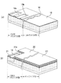
(1)デバイス構造
図1は、本実施例に係る半導体メモリの切り欠き斜視図である。この半導体メモリ10は、一導電型半導体基板であるp型シリコン基板12上に形成されている。p型シリコン基板12は、p+基板12bと、その上のp型エピタキシャル層12aとから成る。p型エピタキシャル層12aには、pウエル13が形成される。
【0076】
また、本発明の特徴を成す凸部13aは、p型シリコン基板12に複数設けられている。ビット線BL1〜BL4は、凸部13a、13a、・・・を挟むpウエル13の表面に形成されている。ビット線BL1〜BL4は、pウエル13の表面の所要部位に、反対導電型であるn型不純物をイオン注入して形成される。同図では他の構成部材に隠れているが、各ビット線BL1〜BL4は、コラム方向に一体化しており、ロウ方向に複数形成される。
【0077】
フローティングゲートFG1、FG2と、コントロールゲートCGはいずれもポリシリコンから成る。コントロールゲートCGは、ロウ方向に一体化しており、コラム方向に複数形成されて、その各々はワード線WL1、WL2、・・・として機能する。
【0078】
コントロールゲートCG、CG、・・・の抵抗を下げるべくWSi膜36が設けられており、コントロールゲートCG、CG、・・・を保護すべくキャップ膜38が設けられており、これは、シリコン酸化膜から成る。
【0079】
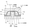
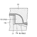
本発明の一特徴を成すセルトランジスタTCの拡大断面図を図2に示す。凸部13aの頂面13cには第1の絶縁膜であるゲート絶縁膜15cが形成されている。また、凸部13aは対向する一対の側面13b、13bを有し、各側面13b、13bの表層には、反対導電型領域であるn型領域17、17が形成されている。このn型領域17, 17の不純物濃度は、上記ビット線BL1、BL2の不純物濃度に比して1/100から1/10000、好ましくは1/1000程度の不純物濃度に選択される。
【0080】
第2の絶縁膜であるトンネル絶縁膜15aは、各側面13b、13bとビット線BL1、BL2とを覆っている。後述するが、ビット線BL1、BL2はソース・ドレイン領域としても機能するので、以下ではビット線BL1、BL2のことをソース・ドレイン領域とも称す。
【0081】
フローティングゲートFG1、FG2は、凸部13aの各側面側に設けられ、各々トンネル絶縁膜15aを介して、ソース・ドレイン領域BL1、BL2および側面13b、13bと対向する。第3の絶縁膜であるインターポリ絶縁膜15bは、フローティングゲートFG、FGの各表面に形成される。
【0082】
なお、トンネル絶縁膜15a、インターポリ絶縁膜15b、およびゲート絶縁膜15cは、いずれもシリコン酸化膜から成る。そして、コントロールゲートCGは、上記インターポリ絶縁膜15bを介してフローティングゲートFG1、FG2と対向し、またゲート絶縁膜15cを介して頂面13cと対向する。このコントロールゲートCGは、上記インターポリ絶縁膜15bを介してフローティングゲートFG1、FG2と対向する部分と、ゲート絶縁膜15cを介して頂面13cと対向する部分とを各々電気的に独立して形成し、これらを独立に電気制御するようにしてもよい。
【0083】
上記の構造では、チャネルは、凸部13aの両側面13b、13bと頂面13cの各表層に三次元的に形成され、従来のように一平面内に形成されていないので、少ない占有面積でチャネル長を稼ぐことができ、デバイスの小型化を図ることができる。
【0084】
凸部13aのp型不純物濃度は、セルトランジスタTCがノーマリーオフとなるように調整される。すなわち、一方のソース・ドレイン領域BL1(BL2)に所定電圧がバイアスされた状態で、このバイアスされたソース・ドレイン領域BL1(BL2)とコントロールゲートCGとの電位差が閾値電圧以下のとき、ゲート絶縁膜15cを介してコントロールゲートCGによって制御される凸部の頂面近傍のチャネル領域がオフ状態となり、その結果、セルトランジスタTCがオフ状態となり、上記電位差が閾値電圧以上のとき、トランジスタTCがオン状態となるように、上記p型不純物濃度は調整される。なお、ソース・ドレイン領域BL1(BL2)にバイアスされる所定電圧とは、書込み、読出し等の各種の動作時に印加される後述の電圧VDDを言う。
【0085】
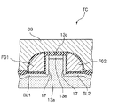
図3は、セルトランジスタTCの等価回路を模式的に表した図であり、様々な容量を示している。各容量の意味は次の通りである。
・CCG ・・・コントロールゲートCGと凸部13aの頂面13cとの対向容量である。
・CCF1(CCF2)・・・コントロールゲートCGとフローティングゲートFG1(FG2)との対向容量である。
・CFG1(CFG2)・・・フローティングゲートFG1(FG2)と、凸部13aの側面13bとの対向容量である。
・CFS(CFD)・・・フローティングゲートFG1(FG2)と、ソース・ドレイン領域BL1(BL2)との対向容量である。
【0086】
再び図1を参照されたい。セルトランジスタTC、TC、・・・は、コラム方向およびロウ方向に複数配列される。コラム方向に隣接するセルトランジスタ(例えばTCaとTCb)同士は、ソース・ドレイン領域BL3、BL4が共通であり、素子分離領域40により電気的に分離される。ロウ方向に隣接するセルトランジスタ(例えばTCcとTCa)は、コントロールゲートCGを共有し、かつ、それらの間のソース・ドレイン領域BL3を共有する。
【0087】
(2)駆動方法
次に、上述のセルトランジスタTCの駆動方法について説明する。
【0088】
I) 書込動作
書込動作について、図4を参照して説明する。図4は、セルトランジスタTCへの書込動作について示す断面図である。上述の如く、凸部13aの両側方には一対のフローティングゲートFG1、FG2が設けられており、本実施例によれば、各フローティングゲートFG1、FG2に独立に電子を注入することができる。
【0089】
例えば、右側のフローティングゲートFG2に電子を注入するには、図4に示すように、コントロールゲートCGに書込電圧VG(たとえば2.2V)を印加する。そして、電子が注入される側のソース・ドレイン領域BL2に電圧VDD(たとえば6V)を印加する。基板12と、電子が注入されない側のソース・ドレイン領域BL1とは接地する。これにより、ソース・ドレイン領域BL1〜BL2間には、書込み用の電位差(本実施例では6V)が与えられる。
【0090】
これによれば、コントロールゲートCGに正電位が印加されるから、頂面13cの表層に反転層13dが形成され、n型領域17、17同士がこの反転層13dにより電気的に接続される。またn型領域17、17は、それと同じ導電型(すなわちn型)のソース・ドレイン領域BL1、BL2に接しているから、結局、ソース・ドレイン領域BL1、BL2が電気的に接続される。
【0091】
従って、キャリア(本実施例では電子)は、同図の矢印の経路を流れることになる。特に、頂面13cを流れる電子に注目されたい。この電子から見れば、その運動方向に右側のフローティングゲートFG2が位置する。よって、電子がこのフローティングゲートFG2に注入されるためには、従来のように電子の運動方向を変える必要が無いから、電子をフローティングゲートFG2に引き付けるためのゲート電圧(書込電圧)VGを従来よりも下げることができる。さらにフローティングゲートFG2は、静電容量の大きなゲート絶縁膜15aを介してドレイン電圧によって電位が引き上げられているから、電子をフローティングゲートFG2に引き付けるためのゲート電圧(書込電圧)VGをさらに下げることができる。
【0092】
しかも、側面13bにn型領域17、17を設けたことで、側面13bが低抵抗となり、そこでの電圧降下が抑えられる。よって、頂面13cの両端に、ソース・ドレイン領域BL1〜BL2間電圧(たとえば6V)より若干低下した高い電圧が印加されるから、この電圧により電子が頂面13cで勢いよく加速され、フローティングゲートFG2に電子が効率良く注入される。このように、n型領域17、17も、書込電圧VGを低減するのに寄与する。
【0093】
上述の利点は、頂面13cでのチャネル抵抗を大きくしても得ることができる。チャネル抵抗を大きくするには、ゲート絶縁膜15cを厚膜に形成して、コントロールゲートCGとチャネル領域との間の静電容量を小さくすれば良い。本実施例では、図4に示すように、ゲート絶縁膜15cをトンネル絶縁膜15aよりも厚くすることで静電容量を小さくし、チャネル抵抗を大きくしている。
【0094】
チャネル抵抗を大きくする構造は上記に限定されず、図5の構造を採用しても良い。この構造では、凸部13aの頂面13cに高抵抗領域(一導電型不純物領域)13eを設ける。係る高抵抗領域13eは、頂面13cに、凸部13aよりも高濃度のp型不純物をイオン注入して形成される。
【0095】
図4または図5のように、頂面13cでのチャネル抵抗を大きくすると、頂面13cでの電圧降下が大きくなるから、頂面13cの両端にソース・ドレイン領域BL1〜BL2間電圧より若干低下した高い電圧が印加される。よって、上述したのと同じ理由により、書込電圧VGを低減することができる。
【0096】
上記を約言すれば、書込電圧VGを低減するには、ii)トンネル絶縁膜の静電容量を大きくして、フローティングゲートをドレイン電圧によって引き上げるか、iii)ゲート絶縁膜15cを厚膜にするか、またはiv)頂面13cに高抵抗領域13eを設ければ良い。これらi)〜iv)を任意に組み合わせることで、上述の利点を得ることもできる。i)〜iv)のいずれの場合であっても、書込電圧VGは約2.2V程度で良く、従来例(約12〜13V)よりも格段に低くすることができる。
【0097】
図4では、右側のフローティングゲートFG2にのみ電子が注入されたが、左側のフローティングゲートFG1に電子を注入するには、ソース・ドレイン領域BL1、BL2の電圧を入れ替えれば良い。よって、本発明では、図6(a)〜(d)に示す4状態が得られる。
【0098】
図6(a)は、両フローティングゲートFG1、FG2に電子が注入されていない“(1、1)”状態を示す。図6(b)、(c)は、フローティングゲートFG1、FG2の一方にのみ電子が注入された“(1、0)”、“(0、1)”状態を示す。図6(d)は、両フローティングゲートFG1、FG2に電子が注入された“(0、0)”状態を示す。この状態を得るには、例えば、右側のフローティングゲートFG2に電子を注入した後、左側のフローティングゲートFG1に電子を注入すれば良い。かくして、本実施例では、1つのセルトランジスタTCに2ビットのデータ“(0、0)”〜“(1、1)”を書き込むことができる。
【0099】
本実施例ではフローティングゲートFG1、FG2が2つ設けられ、各フローティングゲートFG1、FG2に電子が独立に存在するから、セル縮小を図る場合でも、どちらのフローティングゲートFG1、FG2に電子が存在するのかが明確であり、従来例の如くどちらのビットに電子が局在するか不明瞭になることが無い。
【0100】
II)読出動作
次に、読出動作について、図7(a)〜(b)を参照して説明する。データを読み出すには、まず、図7(a)に示すように、コントロールゲートCGに読出電圧VG(たとえば2.2V)を印加する。そして、一方のソース・ドレイン領域BL2に電圧VDD(たとえば1.6V)を印加し、他方のソース・ドレイン領域BL1と基板12とを接地する。これにより、ソース・ドレイン領域BL1〜BL2間には、読出し用の電位差(本実施例では1.6V)が印加される。
【0101】
係る電位配分だと、コントロールゲートCGが正電位となるから、凸部13aの頂面に反転層13dが形成される。よって、同図の矢印の向きに第1のドレイン電流Id1が流れる。
【0102】
次いで、図7(b)に示すように、読出電圧VG(すなわち2.2V)はそのままで、ソース・ドレイン領域BL1、BL2の電圧を入れ替える。このようにすると、ソース・ドレイン領域BL1〜BL2間の電位差が反転するから、同図の矢印の向きに第2のドレイン電流Id2が流れる。
【0103】
本実施例では、上記のようにソース・ドレイン領域BL1、BL2の電圧を入れ替えることにより、2種類のドレイン電流Id1、Id2を計測する。係るドレイン電流Id1、Id2の大きさは、4値状態の各状態によって後述の如く異なる。よって、2種類のドレイン電流値のセット(Id1、Id2)と、各状態とを一対一に対応させることにより、どの状態が記憶されているかを読み出すことができる。次に、各状態“(1、1)”〜“(0、0)”におけるドレイン電流値について説明する。
【0104】
(i)“(1、0)”状態
図8(a)〜(b)は、“(1、0)”状態を読み出す場合の断面図である。図8(a)において、それぞれの部材に印加する電圧は上述の図7(a)の通りであって、係る電圧によりドレイン電流Id1が流れる。図8(a)の状態では、右側のフローティングゲートFG2は、電子が注入されたことにより電位が下がる。しかし、係るフローティングゲートFG2の電位は、対向容量CCF2、CFDによって、コントロールゲートCG(2.2V)やソース・ドレインBL2(1.6V)の正電位側に引き上げられる。
【0105】
結局、フローティングゲートFG2の電位下降が抑えられるから、フローティングゲートFG2近傍でのチャネル抵抗はそれ程大きくない。従って、ドレイン電流Id1の電流値は比較的大きくなる。
【0106】
特に、図のようにn型領域17を設けた場合は、n型領域17はソース・ドレイン領域BL2に接するから、n型領域17の電位がソース・ドレイン領域BL2のそれとほぼ同じとなる。従って、フローティングゲートFG2の電位は、対向容量CFG2によってもソース・ドレインBL2側に引き上げられる。よって、右側のフローティングゲートFG2近傍のチャネル抵抗がさらに小さくなるから、ドレイン電流Id1の電流値はより一層大きくなる。
【0107】
一方、図8(b)は、ソース・ドレインBL1、BL2の電圧を入れ替えて、ドレイン電流Id2を流した場合である。この場合、注入電子によって、右側のフローティングゲートFG2の電位が下がる。しかも、右側のソース・ドレイン領域BL2が接地されるから、フローティングゲートFG2の電位は、ソース・ドレイン領域BL2との対向容量CFDにより接地側に引き下げられる。よって、フローティングゲートFG2の電位が図8(a)の場合よりも低くなるから、フローティングゲートFG2近傍のチャネル抵抗が大きくなり、ドレイン電流Id2が先のId1よりも小さくなる。
【0108】
特に、n型領域17を設けると、右側のフローティングゲートFG2の電位は対向容量CFG2によっても接地側に引き下げられ、ドレイン電流Id2がより一層小さくなる。このように、“(1、0)”状態は、
・(Id1、Id2)=(大、小)
で識別することができる。このドレイン電流Id1、Id2の大小の判定は、不図示のセンスアンプが基準電流と比較して行う。
【0109】
本実施例では、各ドレイン電流Id1、Id2の電流量は、対向容量CCF2、CFD、CFG2によって、上述の如く所望に大にしたり小にしたりすることができる。よって、その差(I d1−Id2)を所望に大きくすることができる。差(I d1−Id2)とは電流ウインドウであるから、本実施例では電流ウインドウを所望に広げることができる。電流ウインドウが広いので、ドレイン電流Id1、Id2と基準電流とのマージンが広くなり、書込データを誤認する危険性が低減できる。
【0110】
(ii)“(0、1)”状態
“(0、1)”状態は、上記とは反対に左側のフローティングゲートFG1に電子が注入される。よって、各ドレイン電流Id1、Id2の電流値は、上記の議論と同様にして評価され、
・(Id1、Id2)=(小、大)
となる。
【0111】
(iii)“(1、1)”状態
“(1、1)”状態は、いずれのフローティングゲートFG1、FG2にも電子が注入されない。従って、各フローティングゲートFG1、FG2の電位は電子によって引き下げられないから、Id1、Id2の双方とも大となる。また、この状態は左右対称であるから、Id1とId2とに差は生じず、
・(Id1、Id2)=(大、大)
となる。
【0112】
(iV)“(0、0)”状態
“(0、0)”状態は、両方のフローティングゲートFG1、FG2に電子が注入されるから、左右対称となる。従って、Id1とId2とに差は生じず、
・(Id1、Id2)=(小、小)
となる。
【0113】
本発明の半導体メモリの読出動作にあっては、上記のごとき“(0, 0)”〜“(1, 1)”論理状態を判定した後、これに基づく読出しを行なってもよいが、以下のようにして読出動作を行なうこともできる。すなわち、本発明の半導体メモリの読出動作にあっては、結局のところ、読出電圧の印加されない側(接地側)のソース・ドレインに対向するフローティングゲートで電荷が蓄積されているか否かに応じてドレイン電流値Idが変化することになる。したがって、一方のソース・ドレインにドレイン電圧を付与した際に、それによって得られるドレイン電流値を検出するのみで、電圧の印加されない側のフローティングゲートの電荷蓄積状況を単独に検出することが可能であり、このようにして読出しを行なうことも可能である。
【0114】
III)消去動作
次に、フローティングゲートFG1、FG2に注入された電子の消去方法について説明する。蓄積電子を引き抜くには、図9に示すように、電子をソース・ドレイン領域BL1、BL2に引き抜く方法が考えられる。この方法では、コントロールゲートCGを接地して、ソース・ドレイン領域BL1、BL2に高電位“H”(たとえば12V)を与える。ここで、コントロールゲートCGと、ソース・ドレイン領域BL1、BL2との電位差は相対的に設定することができ、たとえば、コントロールゲートCGに−6Vを、ソース・ドレイン領域BL1、BL2に6Vを印加するようにしてもよい。
【0115】
他の方法としては、図10に示すように、コントロールゲートCGに高電位VG(たとえば12V)を印加し、基板12とソース・ドレイン領域BL1、BL2とを接地する。この電位配分によれば、フローティングゲートFG1(FG2)から見ると、コントロールゲートCG側の電位が高いので、蓄積電子はインターポリ絶縁膜15bを介してコントロールゲートCGに引き抜かれる。ここでも同様に、コントロールゲートCGに6Vを、ソース・ドレイン領域BL1、BL2に−6Vを印加し、両者間に相対的に12Vの電位差を生じるようにしてもよい。
【0116】
また、図10の電位配分では、コントロールゲートCGが凸部13aよりも高電位だから、図示のように電子層が形成される。この電子層によって、対向容量CFG1(CFG2)の静電容量値が大きくなる。よって、当該対向容量CFG1(CFG2)によって、フローティングゲートFG1(FG2)の電位が、凸部の側面13bの電位に引き付けられる。
【0117】
従って、フローティングゲートFG1(FG2)の電位がより一層下がるから、フローティングFG1(FG2)と側面13bとの電位差が僅かとなり、両者の間のトンネル絶縁膜15aがトンネル電流により破壊されることが無い。
【0118】
その上、フローティングゲートFG1(FG2)の電位がソース・ドレイン領域BL1(BL2)や側面13b側の電位に引き付けられることで、フローティングゲートFG1(FG2)とコントロールゲートCGとの電位差が相対的に増大するから、これらの間に強い電界が生じ、この強電界により蓄積電子がコントロールゲートCGに効率良く引き抜かれる。
【0119】
iv) 非選択時
上記i)〜iii)は、いずれもセルトランジスタ1が選択されている場合であった。実際の動作では、セルトランジスタ1が常に選択されているということはなく、非選択状態の場合もある。
【0120】
非選択状態でも、ビット線BL1(図3参照)には、他のセルトランジスタTCを選択すべく、各動作用の電圧VDDが印加される。この場合、非選択セルトランジスタTCのフローティングゲートFG1は、ビット線BL1との大きい対向容量CFSにより、ビット線BL1の電位に引き付けられる。よって、フローティングゲートFG1とソース・ドレイン領域BL1との間の電位差が小さくなるから、それらの間のトンネル絶縁膜15aが高電界に曝されることが無い。従って、トンネル絶縁膜15aにトンネル電流が流れ難くなり、該トンネル絶縁膜15aが劣化することが防がれる。
【0121】
その上、上記のように電位差が小さくなることから、ソース・ドレイン領域BL1と基板12とのpn接合で高電界によりホットホールが発生することが抑えられるので、当該ホットホールによりトンネル絶縁膜15aが劣化することも防がれる。このように、本実施例ではバンド間トンネル耐性が向上する。
【0122】
ここで、上記駆動時i)〜iv)の各利点を得るために、フローティングゲートFG1(FG2)とソース・ドレイン領域BL1(BL2)との対向容量CFs(CFD)が重要な役割を果たしているのに注意されたい。本実施例では、フローティングゲートFG1(FG2)をソース・ドレイン領域BL1(BL2)上に覆設することにより、フローティングゲートFG1〜FG2の間隔を狭めてデバイスを小型化するとともに、上記対向容量CFD、CFSを大きく稼いで上述の利点を得やすくしている。
【0123】
フローティングゲートFG1(FG2)とソース・ドレイン領域BL1(BL2)との対向面積は限定されない。対向面積が大きいほど上述の利点を得やすいが、小さくても得ることは可能である。従って、図25に示すように、ソース・ドレイン領域BL1(BL2)を凸部13aから後退させ、該ソース・ドレイン領域BL1(BL2)の一部をフローティングゲートFG1(FG2)と対向させても上述の利点が得られる。
【0124】
(3)パンチスルー対策と閾値電圧Vthの安定化
ところで、上記の書き込みや読み出し動作の際に、ソース・ドレインBL1〜BL2間のパンチスルーが問題になるなら、図30に示す構造を採用することが良い。図30中のグラフは、凸部13aの深さと、その深さでのボロン(p型不純物)濃度との関係を示すものである。この構造では、凸部13aのボロン濃度を深さ方向に漸増させて、凸部13aの基端部でのボロン濃度を高くする。このようにすると、ソース・ドレイン領域BL1、BL2に近い部位の側面13b、13bにおいて、ボロン濃度が高くなる。
【0125】
上記の構造により、n型のソース・ドレインBL1、BL2に近い部位のチャネルにおいてp型不純物の濃度が高くなるから、チャネルは、n型のソース・ドレインBL1、BL2を直線的に結んだ領域(n型のソース・ドレインBL1、BL2に近い部位)から離間した領域、すなわち凸部の側面13b, 13bと頂面13cの各表層に形成されることとなる。このことは、上記の構造により、n型のソース・ドレインBL1、BL2に近い部位のチャネルにおいてp型不純物の濃度が高くなるから、ソース・ドレインBL1、BL2がパンチスルーしにくくなることも意味しており、このセルトランジスタを集積化して半導体メモリを形成する場合に、高い集積度を実現することが可能となる。
【0126】
ところで、セルトランジスタTCの閾値電圧Vthは、基端部の側面13b、13bでの不純物濃度に大きく影響される。従って、上述のように基端部でボロン濃度を高くすると、セルトランジスタTCの閾値電圧Vthは高くなる。
【0127】
しかし、側面13bにn型領域17を設けると、このn型領域17中のn型不純物と側面13bのp型不純物とが補償するから、側面13bでの実質的なアクセプタ濃度を下げることができる。よって、たとえ凸部13aの基端部でのボロン濃度を高くしても、n型領域17を設けることで、トランジスタの閾値電圧Vthの増加を抑えることができる。
【0128】
また、上述の如く、閾値電圧Vthは基端部の不純物濃度にデリケートであるから、Vthを安定させるためには基端部で不純物濃度が余り変動しないようにすることが好ましい。従って、凸部13aにおけるボロン濃度は、単に漸増するだけでなく、太線で示すピークをなるべくフラット(平坦)に形成し、フラットな部位を凸部13aの基端部に位置させることが好ましい。フラットな部位では、ボロン濃度が余り変動しないから、ボロン濃度とn型領域17中のヒ素濃度との濃度関係がほぼ一定となり、閾値電圧Vthを安定させることができる。
【0129】
(4)コントロールゲート−ビット線間のリーク電流対策
本実施例では、図11に示すように、ロウ方向に隣接するセルトランジスタTC、TC間のA部において、コントロールゲートCGとビット線BL2とが対向する。よって、A部において、各種の動作時に、コントロールゲートCGとビット線BL2との間にリーク電流が流れることが考えられる。
【0130】
この点が懸念される場合は、図示のように、選択酸化膜34をトンネル絶縁膜15aに繋げて設け、さらに、その厚みをトンネル絶縁膜15aよりも厚膜にすると良い。このようにすると、選択酸化膜34の厚みによって、上記のリーク電流を防ぐことができる。図36の例においては、コントロールゲートCGとビット線BL1, BL2との間のリーク電流を防ぐために、第4の絶縁膜を選択酸化により形成しているが、これに限られるものではなく、隣接するフローティングゲート間に開口を形成して、これに酸化物を充填し、その上に、コントロールゲートCGを形成するようにしてもよい。
【0131】
このようにコントロールゲートCGとビット線BL1, BL2との間に絶縁物が埋められると、フローティングゲートFG1, FG2はコントロールゲートCGと、インターポリ絶縁膜15bを介する部分のみが対向することになる。
【0132】
(5)全体の回路構成
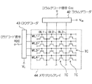
図12に、本実施例全体の回路構成を示す。図12に示す如く、メモリセルアレイ44は、上述のセルトランジスタTC、TC、・・・をコラム方向およびロウ方向に複数配列したものである。各セルトランジスタTC、TC、・・・のコントロールゲート(ワード線)WL1〜WL4は、ロウデコーダ43の出力と接続される。係るロウデコーダ43は、所定ビットのロウデコート゛信号RDCをデコードして、該信号RDCに対応するワード線WL1〜WL4を選択する。
【0133】
選択されたワード線WL1〜WL4には、ゲート電圧VGが供給される。ゲート電圧VGは、書き込み/読出し/消去の各動作時に所望に切り替えられ、各々の動作用の電圧が印加される。上述したように、ゲート電圧VGは、書込み時、2.2V、読出し時、2.2V、消去時、12Vである。一方、ワード線WL1〜WL4は非選択時にはフローティング状態となることがある。
【0134】
一方、各セルトランジスタTC、TC、・・・のビット線BL1〜BL3は、コラムデコーダ42の出力に接続される。コラムデコーダ42は、所定ビットのコラムデコード信号CDCをデコードして、信号CDCに対応するビット線BL1〜BL3を選択する。
【0135】
選択されたビット線BL1〜BL3には電圧VDDが供給される。電圧VDDは、書き込み/読出し/消去の各動作時に所望に切り替えられ、各々の動作用の電圧が印加される。上述したように、電圧VDDは、書込み時、接地または6V、読出し時、接地または1.6V、消去時、接地である。一方、ビット線BL1〜BL3は非選択時にはフローティング状態となることがある。任意のセルトランジスタTCは、選択ビット線BLiと選択ワード線WLjとによって選択されて、書込み/読出し/消去の各動作が行われる。
【0136】
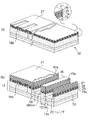
(7)製造プロセス
次に、本実施例に係る半導体メモリの製造方法について、図13〜図24を参照して説明する。最初に、図13(a)に示すように、一導電型半導体基板であるp型シリコン基板12を準備する。p型シリコン基板12は、p+基板(ボロン濃度4.0×1018cm−2)12b上にp型のエピタキシャル層(ボロン濃度1.0×1015cm−2)12aを形成したものである。その表面に、シリコン熱酸化膜18を予め形成しておく。
【0137】
次いで、図13(b)に示すように、シリコン窒化膜19をシリコン熱酸化膜18上に形成する。その後、このシリコン窒化膜19をパターニングして、開口部19aを形成する。
【0138】
本実施例では、セルトランジスタの製造工程を、CMOSトランジスタの製造工程と両立して行うことができる。以下では、セルトランジスタだけでなく、CMOSトランジスタの製造工程も併記する。図中、CMOSトランジスタ部とは、後でCMOSトランジスタが形成される部位を指す。セルトランジスタ部が、セルトランジスタが形成される部位を指す。上述の開口19aは、CMOSトランジスタ部の所要部位に形成する。
【0139】
続いて、図14(a)に示すように、フィールド酸化膜18aを成長させる。係るフィールド酸化膜18aは、シリコン窒化膜19(図13(b)参照)を酸化時のマスクにして成長させる。フィールド酸化膜18aを成長後、このシリコン窒化膜19はエッチングして除去される。
【0140】
次いで、図14(b)に示すように、全体にフォトレジスト20を塗布する。このフォトレジスト20を露光・現像することにより、開口20aを形成する。その後、フォトレジスト20をマスクにし、ヒ素をイオン注入して、開口20aの下にnウエル21を形成する。nウエル21を形成後、フォトレジスト20は除去される。
【0141】
次に、図15(a)に示すように、新たなフォトレジスト22を全体に塗布する。このフォトレジスト22を露光・現像して、開口22aを形成する。その後、フォトレジスト22をマスクにし、ボロンをイオン注入して、開口22aの下にpウエル23を形成する。pウエル23を形成後、フォトレジスト22を除去する。
【0142】
次いで、図15(b)に示すように、全体にフォトレジスト24を塗布する。フォトレジスト24には、露光・現像により、開口24aを形成する。開口24aは、セルトランジスタ部の上方に形成される。このフォトレジスト24をマスクにしてイオン注入を行い、pウエル13を形成する。このイオン注入は4回行われ、各回の条件は次の通りである。
【0143】
・1回目・・・イオン種:BF2
加速エネルギ:15(KeV)
ドーズ量:5.0×10¹¹(cm−2)
・2回目・・・イオン種:BF2
加速エネルギ:45(KeV)
ドーズ量:5.0×10¹¹(cm−2)
・3回目・・・イオン種:B(ボロン)
加速エネルギ:20(KeV)
ドーズ量:6.0×10¹²(cm−2)
・4回目・・・イオン種:B(ボロン)
加速エネルギ:40(KeV)
ドーズ量:5.0×10¹²(cm−2)
ドーズ量:5.0×10¹²(cm −2)
上記4回のイオン注入により、pウエル13は、図31のようなボロン濃度分布を示す。図31は、pウエル13の表面からの深さと、その深さでのボロン濃度との関係を示すグラフである。
【0144】
図において、正味のボロン濃度は、各回のボロン濃度(点線)の包絡線(実線)で表される。これより明らかなように、ボロンの濃度分布にピーク(太線部分)が形成される。ピークを、イオン注入条件を適宜調節してフラットに形成し、フラットな部位を深さ方向にできるだけ広範に存在させることが好ましい。この理由は、後述の図16(b)で明らかになる。
【0145】
次に、図16(a)に示すように、先のフィールド酸化膜18aは残しつつ、シリコン熱酸化膜18(図15(b)参照)をエッチングして除去する。その後、基板12の表面を再び熱酸化し、ゲート絶縁膜15cを形成する。ゲート絶縁膜15cの膜厚は、約10nm程度である。
【0146】
このゲート絶縁膜15c上に、順に、シリコン窒化膜25(たとえば膜厚約10nm)、シリコン酸化膜26(たとえば膜厚4nm)、およびシリコン窒化膜27(たとえば膜厚50nm)を形成する。各膜の機能は、後の工程で明らかになる。これらの膜は、公知のCVD法(化学的気相成長法)により形成される。
【0147】
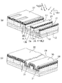
次いで、図16(b)に示すように、最上層のシリコン窒化膜27上にフォトレジスト45を塗布する。塗布後、フォトレジスト45を露光・現像することにより、帯状の開口45a、45a、・・・を形成する。フォトレジスト45をエッチングマスクとして用い、エッチングを行う。エッチングにより、シリコン窒化膜25、27、シリコン酸化膜26、およびゲート絶縁膜15cが開口される。これらの膜の開口を通じてp型シリコン基板12がエッチングされ、トレンチ28、28、・・・が形成される。
【0148】
トレンチ28、28、・・・は、その底部がボロン濃度のピーク(図31参照)に位置するように形成する。ピークは、図15(b)の工程においてフラットに形成され、しかもこのフラットな部位を深さ方向に広範に存在させたから、プロセス上でトレンチ28の深さにばらつきが生じても、トレンチ28の底部をボロン濃度のピークに確実に位置させることができる。
【0149】
これにより、基端部でのボロン濃度が高い凸部13a(図30参照)が形成される。基端部での不純物濃度は、閾値電圧Vthに大きく影響するが、上述のようにトレンチ28の底部をボロンの濃度のピークに確実に位置させることができるから、閾値電圧Vthが変動するのを防ぐことができる。
【0150】
再び、図16(b)に戻ると、トレンチ28、28、・・・のサイズは限定されないが、本実施例ではその深さは約380nm程度である。また、隣接するトレンチ28、28、・・・の間隔(即ち凸部13aの幅)は、約160nm程度である。トレンチ28、28、・・・を形成後、フォトレジスト45は除去される。
【0151】
続いて、図17(a)に示すように、露出面全体にシリコン酸化膜29(膜厚は約20nm)を形成する。シリコン酸化膜29は、CVD法により成膜される。次に、17(b)に示すように、シリコン酸化膜29を厚み方向に異方的にエッチングする。このエッチングは、RIE (Reactive Ion Etching)により行われる。これにより、シリコン酸化膜29は、凸部13aの側面13bに形成されたものを残して、除去される。
【0152】
その後、ヒ素をイオン注入することにより、トレンチ28、28、・・・の底部にビット線BL1、BL2、・・・を形成する。イオン注入の際、側面13bにはシリコン酸化膜29が形成されているから、側面13bにヒ素が注入されることが防がれる。また、凸部13aがマスクとして機能するので、各ビット線BL1、BL2、・・・をトレンチ28の底にセルフアライン的に形成することができる。このイオン注入の条件は次の通りである。
【0153】
イオン種:As(ヒ素)
加速エネルギ:15(KeV)
ドーズ量:2.0×10¹⁴(cm−2)
イオン注入を終了後、側面13bに残存するシリコン酸化膜29を約10nm程度エッチングして薄くする。薄いため、以下では、残存するシリコン酸化膜29の図示を省略する。
【0154】
次いで、図18(a)に示すように、凸部13aの両側面13b、13bにヒ素をイオン注入して、反対導電型領域であるn型領域17、17、・・・を形成する。側面13bにイオン注入するには、基板12をイオンの入射方向に対して傾ければ良い。本実施例では、p型シリコン基板12の法線n1を、イオンの入射方向n0に対して約+/−20°傾ける。このイオン注入の条件は次の通りである。
【0155】
イオン種:As(ヒ素)
加速エネルギ:10(KeV)
ドーズ量:5.0×10¹¹(cm−2)
イオン注入の際、側面13bには薄いシリコン酸化膜29(図17(b)参照)が残存するから、側面13bに過剰にヒ素が注入することを防ぐことができる。
【0156】
ところで、トレンチ28、28、・・・の表層は、デバイスのチャネルとなる部位であり、その性質はデバイスの特性に大きく影響する。よって、後の種々の工程において、トレンチ28、28、・・・の表面が汚染されないようにする必要がある。
【0157】
この点に鑑み、本実施例では、図18(b)に示すように、犠牲シリコン酸化膜31をトレンチ28、28、・・・の側面と底面とに形成する。犠牲シリコン酸化膜31の膜厚は約4nm程度であって、それは熱酸化により形成される。
【0158】
トレンチ28、28、・・・の表面は、犠牲シリコン酸化膜31によって覆われて保護されるから、後の工程で汚染されることが防がれる。しかも、このシリコン酸化膜31は、トレンチ28、28、・・・の表層の格子欠陥を取り除くようにも機能するので、格子欠陥によりデバイスの特性が劣化するのも防がれる。その後、シリコン窒化膜(すなわちマスク膜)30を、トレンチ28、28、・・・内を含む露出面全体に形成する。シリコン窒化膜30の膜厚は約60nm程度であって、それはCVD法により形成される。
【0159】
続いて、図19(a)に示すように、上記のシリコン窒化膜30を厚み方向に異方的にエッチングして、開口である長穴30aを形成する。長穴30aを形成後、シリコン窒化膜30をエッチングマスクにし、先の犠牲シリコン酸化膜31と、各ビット線BL1、BL2、・・・の一部とを選択的にエッチングする。エッチングにより、各ビット線BL1、BL2、・・・には、リセス(窪み)32(深さ約10nm)が形成される。
【0160】
その後、ビット線BL1、BL2、・・・の抵抗を下げるべく、長穴30aを通じて、ヒ素をビット線BL1、BL2、・・・にイオン注入する。図に、イオン注入によりヒ素が注入された部位(n+領域)33を示す。イオン注入の条件は次の通りである。
【0161】
イオン種:As(ヒ素)
加速エネルギ:30(KeV)
ドーズ量:3.0×10¹⁵(cm−2)
次いで、図19(b)に示すように、シリコン窒化膜30をマスクにし、リセス32、32、・・・を選択的に酸化して選択酸化膜34、34、・・・を形成する。選択酸化膜34、34、・・・を形成した後は、シリコン窒化膜27、30をエッチングして除去する。エッチングでは、シリコン酸化膜26と犠牲シリコン酸化膜31とがエッチングストッパして機能する。次いで、シリコン酸化膜26をエッチングして除去する。今度は、シリコン窒化膜25がエッチングストッパとして機能する。エッチングは、シリコン酸化膜26が完全に除去され、かつ、選択酸化膜34、34、・・・が残存する程度に行う。
【0162】
その後、図20(a)に示すように、トレンチ28、28、・・・の底面と側面とを再び酸化して、膜厚が約5nm程度のトンネル絶縁膜15aを形成する。トンネル絶縁膜15aは、その膜質がデバイス動作に大きく影響するから、良好な膜質になるように形成することが好ましい。
【0163】
本実施例では、良質なトンネル絶縁膜15aを形成すべく、プラズマ酸化法を用いる。プラズマ酸化法においては、ラジアルラインスロットアンテナを使用したマイクロ波励起高密度プラズマ装置が用いられる。そして、該装置内に、クリプトン(Kr)と酸素(O2)との混合ガスを導入する。
【0164】
マイクロ波により励起されたクリプトンは、酸素(O2)と衝突して大量の原子状酸素O*を生成せしめる。原子状酸素O*は、トレンチ28、28、・・・の表層部に容易に浸入する。よって、面方位に依存することなく、全ての面方位が概略同じ酸化速度で均一に酸化される。そのため、同図の円内に示す如く、トレンチ28、28、・・・のコーナ部に均一な膜厚でトンネル絶縁膜15aが形成できる。なお、上記のプラズマ酸化法については、「第48回応用物理学関係連合講演会 講演予稿集 29p−YC−4」や、特開2001−160555号公報に詳しい。
【0165】
上記のようにトンネル絶縁膜15aを形成した後は、図20(b)の工程が行われる。この工程では、ポリシリコン膜34を、上記トンネル絶縁膜15a上とシリコン窒化膜25上とに形成する。ポリシリコン膜34は、in−situでリン(P)が予めドープされている。また、このポリシリコン膜34の膜厚は、約50nm程度である。
【0166】
次に、図21(a)に示すように、ポリシリコン膜34を厚み方向に異方的にエッチングする。これにより、シリコン窒化膜25上のポリシリコン膜34を除去しつつ、トレンチ28、28、・・・の側面上のトンネル絶縁膜15a上にポリシリコン膜34を残存させる。残存したポリシリコン膜34は、フローティングゲートFG1、FG2となる。フローティングゲートFG1、FG2を形成後、シリコン窒化膜25をエッチングして除去する。
【0167】
続いて、図21(b)に示すように、全体にフォトレジスト35を塗布する。塗布後、フォトレジスト35を露光・現像することにより、開口35aを形成する。この開口35aは、CMOSトランジスタ部上に形成する。このフォトレジスト35をエッチングマスクとして使用し、CMOSトランジスタ部上のゲート絶縁膜15cをエッチングする。これにより、CMOSトランジスタ部のnウエル21とpウエル23の表面が露出する。
【0168】
次いで、図22(a)に示すように、フォトレジスト35を除去後、露出面全体を既述のプラズマ酸化法により酸化する。これにより、ゲート絶縁膜15c下のシリコンが酸化されるから、ゲート絶縁膜15cが厚膜となる。同時に、フローティングゲートFG1、FG2の表面も酸化され、インターポリ絶縁膜15bが形成される。インターポリ絶縁膜15bの膜厚は、約8nm程度である。
【0169】
フローティングゲートFG1、FG2は、ポリシリコンから成るので、その表面には様々な面方位の結晶粒が多数形成されている。このように面方位がまちまちでも、上述のプラズマ酸化法によれば、面方位に依存すること無しに、均一にシリコン酸化膜が形成できる。よって、インターポリ絶縁膜15bの膜厚が局所的に薄くなることが防がれ、薄い部位での絶縁特性が劣化するという不都合が生じない。この利点は、ポリシリコンにリン(P)がドープされていても得ることができる。
【0170】
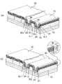
続いて、図22(b)に示す構造を作製する。この構造を得るには、まず、露出面全体にポリシリコン膜を形成する。このポリシリコン膜は後でコントロールゲートCGとなる。ポリシリコン膜は、in−situプロセスでリン(P)が予めドープされている。次いで、ポリシリコン膜上に、WSi膜36を形成する。さらに、WSi膜36上に、シリコン酸化膜からなるキャップ膜38を形成する。そして、これらの積層膜をパターニングすることで、図示の構造が得られる。
【0171】
この工程により、ロウ方向に一体化して成るコントロールゲートCG、CG、・・・が複数形成される。同時に、CMOSトランジスタ部上のpウエル23、nウエル21上に、ゲート電極41が形成される。ゲート電極41は、ポリシリコン膜37を主体に構成され、WSi膜36により、その抵抗が下げられている。WSi膜36は、コントロールゲートCG上にも形成されるから、コントロールゲートCGの抵抗も下がる。
【0172】
次いで、図23(a)に示すように、全体にフォトレジスト39を塗布する。塗布後、フォトレジスト39を露光・現像することにより、開口39aを形成する。開口39aを形成する部位は、隣接するコントロールゲートCG、CG、・・・の間である。
【0173】
続いて、図23(b)に示すように、フォトレジスト39をエッチングマスクとして使用し、コントロールゲートCG、CG、・・・で覆われていない部位のインターポリ絶縁膜15bをエッチングして除去する。エッチングの際、コントロールゲートCG、CG、・・・間のゲート絶縁膜15cも僅かにエッチングされる。さらに、エッチャントを変えて、コントロールゲートCG、CG、・・・で覆われていない部位のフローティングゲートFG1、FG2をエッチングして除去する。この工程により、隣接するコントロールゲートCG、CG、・・・の間に、トンネル絶縁膜15aが露出する。
【0174】
最後に、図24に示すように、素子分離領域40を形成する。この素子分離領域40を形成すべき部位は、コントロールゲートCG、CG、・・・で覆われていない凸部13aの、側面13bおよび頂面13cである。側面13bおよび頂面13cは、コントロールゲートCG下でチャネルとなるが、素子分離領域40によって、隣接するコントロールCG、CG下のチャネルが電気的に分離される。
【0175】
素子分離領域40を形成するには、フォトレジスト39をマスクにして、ボロンをイオン注入する。イオン注入に際しては、素子分離領域40を凸部13aの側面13bに形成すべく、基板12をイオンの入射方向に対して傾ける。本実施例では、p型シリコン基板12の法線n1を、イオンの入射方向noに対して約+/−20°傾ける。イオン注入の条件は次の通りである。
・イオン種:BF2
・加速エネルギ:20(KeV)
・ドーズ量:1.0×10¹³(cm−2)
その後、フォトレジスト39を除去することで、図1に示される半導体メモリ10が完成する。なお、CMOSトランジスタ部については、所要部位にソース・ドレイン領域を形成して完成させる。
【0176】
次に本発明の他の実施例について説明する。本実施例では、メモリセルを過消去することに1つの特徴がある。本実施例は、フローティングゲートに蓄積された電荷を実質的に0以下の状態となるように過消去させることにより、書込効率が改善され、書込速度が向上することに着目したものである。
【0177】
なお、本実施例においては、フローティングゲートが、2つの反対導電型領域の間にあるチャネル領域の一部にのみ設けられている半導体メモリを対象としているため、コントロールゲートを接地することにより、フローティングゲートが設けられていないチャネル領域において電流を遮断することができ、読出し時等において選択されていないメモリセルに電流が流れることを防ぐことができる。すなわち、読出し時等において選択されていないメモリセルのコントロールゲートを接地しているときに、電流が流れることはないからである。さらに、過消去により、電流ウィンドウマージン(すなわちフローティングゲートに電荷が蓄積されているときと、いないときの電流差)が大きくなるという利点もある。
【0178】
本実施例では、過消去は、消去したいメモリセルに対して前述の消去動作を、当該メモリセルに過消去が生じる時間、たとえば5msecの間、実行することにより行う。この程度の時間が経過すると、フローティングゲートの過消去状態で消去動作は飽和状態となり安定した電荷喪失状態(電子欠乏状態、正孔蓄積状態)となり、FN電流値は、ほぼ0となって、フローティングゲートに、これ以上の正の電荷が蓄積されることはない。
【0179】
次に、本実施例に係る半導体メモリについて具体的に説明する。以下の説明では、既述の実施例の構成要素と同一の機能を有するものについては同一の参照符号を用いることとし、その説明も一部省略する。
【0180】
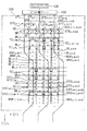
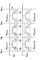
本実施例に係る半導体メモリの回路構成について説明する。図32は、本実施例に係る半導体メモリアレイ126の回路構成図である。同図において、参照符号TCi ,m,pはiロウmコラム目(i=0,1,2,・・・、m=0,1,2,・・・)のバンクBNKi,m内のp番目(p=0,1,2,・・・)のセルトランジスタを表し、その構造と動作は、上述の図2に示すトランジスタと同一である。
【0181】
セルトランジスタTCi ,m,pの各々は、バンクBNKi,mにバンク分けされ、図1を参照して前述したTCに相当する。各バンクBNKi,mは、(1コラム)×(nロウ)に配列されたn個のセルトランジスタTCi ,m,pからなる。なお、nは所定の自然数を表し、その値はとくに限定されない。また、バンクBNKi,mにおけるiおよびmは、そのバンクに属するセルトランジスタTCi ,m,Pの共通のロウ番号およびコラム番号をそれぞれ表す。
【0182】
この回路では、通常のフラッシュメモリがワード線とビット線との組み合わせでセルトランジスタを選択するのに対して、まず、iロウにある偶数バンク群BNKi,m(m=0,2,4・・・)と奇数バンク群BNKi,m(m=1,3,5・・・)のいずれか一方の群を選択線SEi, SOiを用いて選択し、当該バンク群からビット線BLm(m=0,1,2,・・・)を用いて(より正確には、ビット線BLmに接続された仮想接地線VTKを用いて)、1つのバンクを選択し、次いでそのバンクBNKi,m内の一つのセルトランジスタTCi ,m,pをワード線WLpを用いて選択する。以下、これを具体的に説明する。
【0183】
各バンクBNKi,mには、それを選択するための選択トランジスタSTEi ,m, STOi ,mが1個ずつ接続されている。このうち、選択トランジスタSTEi ,mは、iロウにあるバンクBNKi,mのうち、コラム番号が偶数であるバンクBNKi,m(m=0,2,4・・・)を選択するためのものであって、以下では偶数バンク選択トランジスタとも言う。選択トランジスタSTEi ,mを指定するために、選択線SEiを用いる。1本の選択線SEiには、iロウに配列されたすべての選択トランジスタSTEi ,m(m=0,1,2,・・・)が接続されている。選択線SEiにより、選択線SEiに接続されたすべての選択トランジスタSTEi ,m(m=0,1,2,・・・)が選択される。
【0184】
また、選択トランジスタSTOi, mはiロウにあるバンクBNKi,mのうち、コラム番号が奇数であるバンクBNKi,m(m=1,3,5・・・)を選択するためのものであって、以下では奇数バンク選択トランジスタとも言う。選択トランジスタSTOi ,mを指定するために、選択線SOiを用いる。1本の選択線SOiには、iロウに配列されたすべての選択トランジスタSTOi ,m(m=0,1,2,・・・)が接続されている。選択線SOiにより、選択線SOiに接続されたすべての選択トランジスタSTOi ,m(m=0,1,2,・・・)が選択される。
【0185】
同図に示されるように、偶数バンク選択トランジスタSTEi, mの各々は、それらの一方のソース・ドレインが1コラムおきに共通接続され、その共通接続ノードA, D, Eに仮想接地線VTk(k=0,1,2,・・・)が接続されている。
【0186】
奇数バンク選択トランジスタSTOi, mも同様であるが、その共通接続点は、偶数バンク選択トランジスタSTEi, mのそれよりも1コラムだけずれている。
【0187】
なお、図中、符号STEi−1 ,m(m=O,2,・・・)は、コラム方向に数えてi−1番目のバンク中、偶数バンクを選択するための偶数バンク選択トランジスタである。これに対して、符号STOi+1,m(m=1, ,・・・)は、コラム方向に数えてi+1番目のバンク中、奇数バンクを選択するための奇数バンク選択トランジスタである。
【0188】
また、仮想接地線VTk(k=0,1,2,・・・)は、その電気抵抗を減らすべく、アルミニウム等の金属からなる。一方、ビット線BLm(m=0,1,2・・・)は拡散層からなり、その電気抵抗は仮想接地線VTkのそれよりもずっと高い。
【0189】
回路動作は次の通りである。例えば、読出し時に同図中のセルトランジスタTCi,m,0を選択する場合を考える(ここでは、mは偶数と仮定する)。セルトランジスタTCi,m,0は偶数バンクBNKi,mに属する。よって、まず偶数バンク群BNKi,m(m=0,2,4・・・)を選択すべく、偶数バンク選択線SEiをハイレベルにし、各偶数バンク選択トランジスタSTEi,m(m=0,1,2・・・)をオン状態にする。その他の選択線(SEr(r=0,1,2,・・・,i−1,i+1,・・・)、SOr(r=0,1,2,・・・))はすべてローレベルにし、その選択線がゲートに接続されるトランジスタをすべてオフ状態にする。
【0190】
上述の電圧配分によれば、オン状態の偶数バンク選択トランジスタSTEi,m、STEi,m+1によって、ビット線BLm, BLm+1が仮想接地線VTk, VTk+1に電気的に接続状態となる。他の偶数バンクBNKi,m−2, BNKi,m+4等に繋がるビット線も同様にして仮想接地線と電気的に接続状態となる。
【0191】
次いで、目的のセルトランジスタTCi,m,0を選択するため、それにビット線BLmを介して繋がる仮想接地線VTkを接地レベルにし、かつビット線BLm+1を介して繋がる仮想接地線VTk +1に低い電圧VDD(=1.6V)を印加する。それ以外の仮想接地線VTはオープン状態にする。このようにして、まず偶数バンク群i,m(m=0,2,4・・・)が選択される。具体的に、このように仮想接地線VTを設定することは、仮想接地線VTに接続されたビット線ゲート122が行う。ビット線ゲート122の詳細は後述する。そして、ワード線WL0に読出し電圧VG(=2.2V)を印加する。さらに、仮想接地線VTに接続されたビット線ゲート122により、仮想接地線VTk +1のみをセンスアンプ128に接続し、仮想接地線VTk +1に流れる電流をセンスアンプ128により検知する。
【0192】
ソース・ドレインに印加されたこれらの電圧値により、図8(a)で説明したように、セルトランジスタTCi,m,0に第1のドレイン電流Id1が流れる。この第1のドレイン電流Id1は、センスアンプ128からビット線ゲート122、仮想接地線VGk+1、ノードD、ノードC、偶数バンク選択トランジスタSTEi,m+1、ビット線BLm+1、セルトランジスタTCi,m,0、ビット線BLm、偶数バンク選択トランジスタSTEi,m、ノードB、ノードA、仮想接地線VGk、ビット線ゲート122の順に流れる。
【0193】
次いで、ビット線ゲート122により、ビット線BLmとBLm+1との間の電位差を反転させ、それ以外の電圧値を上記と同様のままにしておく。このようにすると、図8(b)で説明したように、セルトランジスタTCi,m,0に第2のドレイン電流Id2が流れる。この第2のドレイン電流Id2の電流経路は、第1のドレイン電流Id1のそれの逆である。
【0194】
このようにしてセルトランジスタTCi,m,0の第1のドレイン電流Id1および第2のドレイン電流Id2がセンスアンプにより計測され、セルトランジスタTCi,m,0に4値状態“(0, 0)”〜“(1, 1)”のいずれが記憶されているかが識別される。
【0195】
この回路構成によれば、第1のドレイン電流Id1は、拡散層からなる高抵抗のビット線BLm、BLm+1内を常に流れるという訳ではなく、目的のバンクBNKi,mに到達するまでは低抵抗の仮想接地線VGk+1内を流れ、目的のバンクBNKi,mに到達してからビット線BLm+1を流れるようになる。そして、セルトランジスタTCi,m.0を流れた後、第1のドレイン電流Id1はビット線BLmを経由して仮想接地線VGkを流れる。
【0196】
このように、常にビット線BLm, BLm+1内を流れる場合よりも低抵抗なので、本実施例では第1のドレイン電流Id1を高速で読み出すことが可能となる。第2のドレイン電流Id2についても同様の利点が得られる。
【0197】
上述の例では、偶数バンクBNKi,m内のセルトランジスタTCi,m,0が選択された。一方、奇数バンク群BNKi,m(m=1,3,5・・・)内のセルトランジスタをTCi,m,pを選択するには、奇数バンク選択線SOiをハイレベルにし、各奇数バンク選択トランジスタSTOi,m(m=0,1,2・・・)をオン状態にする。そして、その他の選択線(SEr(r=0,1,2,・・・)、SOr(r=0,1,2,・・・,i−1,i+1,・・・))はすべてローレベルにし、これらの選択線がゲートに接続されるトランジスタをすべてオフ状態にする。これ以外は偶数バンクを選択する場合と同様なので、奇数バンクについてはこれ以上説明しない。上述したセルトランジスタの選択方法は仮想接地方式とも称される。
【0198】
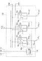
図33は、本発明に係わる半導体メモリの一実施例の構成を示す機能ブロック図である。本実施例の半導体メモリはフラッシュメモリ120である。
【0199】
図33のフラッシュメモリ120は、アドレス信号線124を介してアドレス信号124を受け取る。また、データ線146を介して、書込データ146を入力され、また読出データ146を出力する。アドレス信号124は、メモリアレイ126内のメモリセルのうちのいずれに対してデータ読出しまたはデータ書込みを行うかを指示する信号である。
【0200】
なお、消去は、通常たとえば64Kバイト単位で一括して行う。その際に、64Kバイトのセルのうち、1つのロウに繋がったセルのすべてについて一度に消去を行ない、順次各ロウに対して消去を行なって、64Kバイトのセルの一括消去を行なう。
【0201】
書込データ146および読出データ146は、たとえば8ビットのデータである。ただし、以下では、説明を簡単にするために、書込データ146および読出データ146は、2ビット(1メモリセル分)であり、消去は、全メモリセルに対して一括して一度に行われるとする。
【0202】
制御部130は、入力されたアドレス信号124を蓄積して、アドレス信号124から、バンクデータ132と、ワードデータ134と、ビット線データ136とを生成し、それぞれ、バンクデコーダ138、ワードデコーダ140、ビット線ゲート122に出力する。また、制御部130は、バンクデコーダ138、ワードデコーダ140、ビット線ゲート122に対して、書込動作、読出動作、消去動作のいずれを行うかを示す情報(以下ではモード情報と呼ぶ)を信号線150を介して出力する。制御部130自体は、モード情報を外部から、図示しない信号線を介して受け取り、バンクデコーダ138、ワードデコーダ140、ビット線ゲート122に対して、モード情報として出力する。
【0203】
制御部130は、書込動作時に書込データ146を、信号線148を介して書込データ148としてビット線ゲート122に送る。ビット線ゲート122は、ビット線データ136で指定された仮想接地線VTに対して、書込データ148に応じて、仮想接地線VTに6.0Vを印加するか(ドレイン側)、もしくは仮想接地線VTを接地する(ソース側)。ただし書込み時、書込データが(1, 1)である場合は、書込みを行う必要がないため、制御部130は書込動作を、各部に対して指示しない。
【0204】
読出データ146に関しては、制御部130は読出動作時に、センスアンプ128から信号線142を介して送られてくるデータ142に基づいて生成する。すなわち、1つのメモリセルに対してビット線ゲート122は、ドレインとソースを入れ替えて2回の読出しを行う。制御部130は、センスアンプ128から信号線142を介して送られてくる2つの信号142(これは既述のId1, Id2から生成された信号である)から、(Id1, Id2)が、(大、大)、(大、小)、(小、大)、(小、小)のいずれであるかを判定して、読出しデータ146を生成する。
【0205】
本発明の半導体メモリの読出動作にあっては、上記のごとき“(0, 0)”〜“(1, 1)”論理状態を判定した後、これに基づく読出しを行なってもよいが、以下のようにして読出動作を行なうこともできる。すなわち、本発明の半導体メモリの読出動作にあっては、結局のところ、読出電圧の印加されない側(接地側)のソース・ドレインに対向するフローティングゲートで電荷が蓄積されているか否かに応じてドレイン電流値Idが変化することになる。したがって、一方のソース・ドレインにドレイン電圧を付与した際に、それによって得られるドレイン電流値を検出するのみで、電圧の印加されない側のフローティングゲートの電荷蓄積状況を単独に検出することが可能であり、このようにして読出しを行なうことも可能である。
【0206】
バンクデコーダ138は、制御部130からバンクデータ132を入力されて、メモリアレイ126内の選択線SE, SOのうちのいずれか1本(読出動作時および書込動作時)、もしくはすべて(消去動作時)を選択することにより、当該選択線に接続されたバンク選択トランジスタを選択する。選択は、選択された選択線SE, SOに、選択トランジスタSTE, STOのゲートしきい値電圧以上の電圧を印加することにより行う。選択されなかった選択線SE, SOには、選択トランジスタSTE, STOのゲートしきい値電圧より小さい電圧を印加して、ビット線BLと仮想接地線VTとを非接続にする。
【0207】
ワードデコーダ140は、制御部130からワードデータ134を入力されて、メモリアレイ126内のワード線WLのうちのいずれか1本(読出動作時および書込動作時)、もしくはすべて(消去動作時)を選択する。そして、選択したワード線WLに、電源部144から入力される電圧VE, VW, VRを供給する。ここで電圧VEは、消去時にセルトランジスタTCのコントロールゲートに印加される電圧(たとえば12V)、電圧VWは、書込み時にセルトランジスタTCのコントロールゲートに印加される電圧(たとえば2.2V)、電圧VRは、読出し時にセルトランジスタTCのコントロールゲートに印加される電圧(たとえば2.2V)である。消去時には、ワードデコーダ140は、過消去を行なうために、ワード線WLに電圧VEを5msecの間、印加する。
【0208】
なお、フローティングゲートへのデータの書込みは、書込可能な書込電圧値のうち、最小の電圧値の近傍にある書込電圧VWを用いて行うことが好ましい。このとき書込効率が最大となるためである。ここで書込効率とは、フローティングゲートに注入される電流Ifgとソース電流Isとの比、Ifg/Isをいう。
【0209】
選択されなかったワード線WLには、セルトランジスタTCのゲートしきい値電圧より小さい電圧を印加して、選択されなかったセルトランジスタTCに電流が流れることを防ぐ。小さい電圧を印加するために、通常は、ワード線を接地する。
【0210】
ビット線ゲート122は、読出動作時および書込動作時に、制御部130からビット線データ136を入力されて、メモリアレイ126内の1コラム内のバンクBNKi,m(i=0,1,2,・・・)に含まれるセルトランジスタTCi,m,p(i=0,1,2,・・・)を選択するように、仮想接地線VTに所定の電圧を印加する。消去動作時はすべてのバンク、すなわちすべてのセルトランジスタを選択して、そのドレインとソースを接地する。選択されなかったバンクに接続された仮想接地線VTはオープン状態にする。以下、これについて図34を参照して詳述する。
【0211】
図34は、ビット線ゲート122の構成例を示すブロック図である。ビット線ゲート122のビット線制御部152は制御部130から、ビット線データ136、書込データ148(書込動作時のみ)、モード情報150を入力される。ビット線データ136は、具体的にはたとえば書込みまたは読出し対象のバンクBNKi,mのコラム番号mである。
【0212】
ビット線制御部152は、ビット線データ136を入力されると、対象となるバンクBNKi,m内のドレイン側のビット線BLに接続された仮想接地線VTと、ソース側のビット線BLに接続された仮想接地線VTに所定の電圧を、スイッチ54k(k=0,1,2,・・・)を介して印加する。これ以外の仮想接地線VTは、スイッチ54kによってオープン状態にする。このために、ビット線制御部152は、各スイッチ54kに対して、電圧指示信号56k(k=0,1,2,・・・)を出力する。
【0213】
スイッチ54kは、仮想接地線VTkごとに設けられており、電圧指示信号56kを入力されて、仮想接地線VTkに所定の電圧を印加すること、もしくは仮想接地線VTkとセンスアンプ128とを接続することを行う。
【0214】
スイッチ54kは、いずれも同一の構成を有しており、端子58a, 58b, 58cを含む。端子58aには、電源部144から電圧VDWが供給され、端子58bは、信号線60を介してセンスアンプ128と接続され、端子58cは接地されている。書込動作時は、ドレイン側の仮想接地線VTを端子58aに接続して、電圧VDWを印加し、ソース側の仮想接地線VTを端子58cに接続して接地し、他の仮想接地線VTは、端子58a, 58b, 58cのいずれにも接続しないオープン状態にする。
【0215】
書込データが(0, 0)の場合は、上記の操作によりドレインに電荷を蓄積した後、ドレイン側とソース側を入れ替えて、すなわち端子58aに接続した仮想接地線VTを端子58cに接続し、端子58cに接続した仮想接地線VTを端子58aに接続して、入れ替え後のドレインにも電荷を蓄積する。
【0216】
読出動作時は、ドレイン側の仮想接地線VTを端子58bに接続して、センスアンプ128に接続し、ソース側の仮想接地線VTを端子58cに接続して接地し、他の仮想接地線VTは、端子58a, 58b, 58cのいずれにも接続しないオープン状態にする。こうして、セルトランジスタTCに流れる電流をセンスアンプ128で検知する。読出動作時はドレイン側に低い電圧1.6Vを印加する必要があるが、これは、センスアンプ128を介して行なう。
【0217】
次に、ドレイン側とソース側を入れ替えて、すなわち端子58bに接続した仮想接地線VTを端子58cに接続し、端子58cに接続した仮想接地線VTを端子58bに接続し、他の仮想接地線VTの接続は変更しないで、再度、セルトランジスタTCに流れる電流をセンスアンプ128により検知する。
【0218】
図34に示す仮想接地線VTの接続状態は、読出動作時のものであり、仮想接地線VTk+1がドレイン側(端子58b)、仮想接地線VTkがソース側(端子58c)の場合であり、仮想接地線VTk+2はオープン状態にある。この場合、図32のm番目のコラムを構成するバンクBNKi,m(i=0,1,2,・・・)のみが読出しの対象として選択されている。読出動作時は、ドレインとソースを入れ替えて2回の読出しを行なうため、図34の接続状態で読出しを行なった後、仮想接地線VTk+1をソース側(端子58c)に、仮想接地線VTkをドレイン側(端子58b)に接続する。仮想接地線VTk+2はオープン状態のままである。これで、1つのセルトランジスタに対する読出動作が終了する。
【0219】
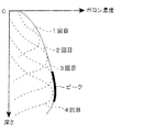
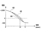
消去動作時は、すべての仮想接地線VTを本実施例では5msecの間、端子58cに接続して、仮想接地線VTを接地する。5msecという時間は、次のような考え方に基づいて設定されている。フローティングゲートに蓄積された電荷(この場合は電子)は、FN電流を用いて消去される。消去時に、時間の経過とともに、フローティングゲートに蓄積された電子の数が減っていく様子の一例を図35に示す。
【0220】
本図は、1個のフローティングゲートに蓄積された電子の数を、消去開始時からの時間の関数として表示した曲線66を示す。縦軸は電子の数を示し、消去開始時の電子の数は1000個とした。時刻t1において、電子の数が「0」個となり、その後は、正の電荷(ホール(hole))が蓄積されることを示す。5msec経過したときにフローティングゲートに蓄積された正の電荷の数は、500個である。このときに、FN電流値は、ほぼ「0」となっている。この後は、蓄積された正の電荷の数は、ほぼ変化しない。
【0221】
ところで、実際の消去における電子の数の減り方にはばらつきがある。これを示すために、平均的な減り方を示す実線の曲線66に対して、減り方が速い場合の曲線64と、遅い場合の曲線62を図中に点線で示す。曲線66, 62, 64からわかるように、電子の数の減り方の特徴は、減少している途中においては、減り方に幅、すなわちばらつきがあり、電子の数が「0」個になるときの時刻は変動する。一方、最終的にFN電流が「0」になったときの電子数には変動がない。
【0222】
このため、従来のように電子数が「0」個の近傍(時刻t1)で消去を停止させようとすると、ばらつきを考慮した対策が必要であった。たとえば、過消去されないように、少しずつ消去を行い、そのたびに過消去されていないことをベリファイすることが必要があった。本実施例のように、FN電流の値が「0」になる近傍まで過消去させる場合、この電子が欠乏した状態にはばらつきがほとんどない。すなわち電荷数が飽和した状態となり、安定したゲートしきい値電圧が得られる。このため、ベリファイという操作が不要となる利点もある。
【0223】
なお、本発明は、FN電流の値が「0」になるまで過消去を行う場合に限られるものではなく、FN電流の値が所定値より少なくなるまで、フローティングゲートに蓄積された電荷を消去して、過消去を行うこととしてもよい。また、フローティングゲートに蓄積された正の電荷が所定数以上になるまで、たとえば、500個以上になるまで、過消去を行なうこととしてもよい。
【0224】
以上の説明からわかるように、本実施例の場合、選択手段は、バンクデコーダ138とワードデコーダ140とビット線ゲート122とから構成され、過消去手段は、ワードデコーダ140とビット線ゲート122と電源部144とから構成されている。また書込手段は、ワードデコーダ140とビット線ゲート122と電源部144から構成されている。
【0225】
図33に戻って、センスアンプ128は、読出動作時にビット線ゲート122により、読出対象であるセルトランジスタTCのドレイン側に接続され、セルトランジスタTCに流れる電流の大小を検知する。検知結果は、信号線142を介して制御部130に送られる。読出データ142はたとえば、高い電圧と低い電圧であり、高い電圧が電流「大」に対応し、低い電圧が電流「小」に対応する。電源部144は、ワードデコーダ140に電圧VE, VW, VRを供給し、ビット線ゲート122に電圧VDWを供給する。
【0226】
次に、上述のように構成されたフラッシュメモリ120の動作について述べる。書込動作時、制御部130は、外部から書込み指示と、書込み対象であるアドレス信号124と、書込データ146とを受け取る。制御部130は、アドレス信号124から、バンクデータ132と、ワードデータ134と、ビット線データ136とを生成し、それぞれ、バンクデコーダ138、ワードデコーダ140、ビット線ゲート122に出力する。また、バンクデコーダ138、ワードデコーダ140、ビット線ゲート122に対して、書込みであることを示すモード情報を出力する。さらに、書込データ146を、信号線148を介して書込データ148としてビット線ゲート122に送る。
【0227】
バンクデコーダ138は、制御部130から入力されたモード情報により、書込動作を行う。すなわちバンクデータ132に従って、メモリアレイ126内の選択線SE, SOのうちのいずれか1本にのみ、バンク選択トランジスタSTO, STEのゲートしきい値電圧以上の電圧を印加し、他の選択線SE, SOは接地することにより、当該選択線に接続されたバンク選択トランジスタのみを選択する。
【0228】
ワードデコーダ140は、制御部130から入力されたモード情報により、書込動作を行う。すなわちワードデータ134に従って、メモリアレイ126内のワード線WLのうちのいずれか1本を選択して、選択したワード線WLにのみ、電源部144から入力された電圧VWを供給し、他のワード線WLは接地する。
【0229】
ビット線ゲート122は、制御部130から入力されたモード情報により、書込動作を行う。すなわちビット線データ136と、書込データ148に従って、指定されたビット線、すなわち仮想接地線のうち、ドレイン側ビット線に電圧VDWを印加し、ソース側ビット線を接地する。書込データが(0, 0)の場合は、この操作によりドレインに電荷を蓄積した後、ドレイン側とソース側を入れ替えて、入れ替え後のドレインにも電荷を蓄積する。
【0230】
読出動作時、制御部130は、外部から読込み指示と、読込み対象であるアドレス信号124とを受け取る。制御部130は、アドレス信号124から、バンクデータ132と、ワードデータ134と、ビット線データ136とを生成し、それぞれ、バンクデコーダ138、ワードデコーダ140、ビット線ゲート122に出力する。また、バンクデコーダ138、ワードデコーダ140、ビット線ゲート122に対して、読込みであることを示すモード情報を出力する。
【0231】
バンクデコーダ138は、制御部130から入力されたモード情報により、読出動作を行う。すなわちバンクデータ132に従って、メモリアレイ126内の選択線SE, SOのうちのいずれか1本にのみ、バンク選択トランジスタSTO, STEのゲートしきい値電圧以上の電圧を印加し、他の選択線SE, SOは接地することにより、当該選択線に接続されたバンク選択トランジスタのみを選択する。
【0232】
ワードデコーダ140は、制御部130から入力されたモード情報により、読出動作を行う。すなわちワードデータ134に従って、メモリアレイ126内のワード線WLのうちのいずれか1本を選択して、選択したワード線WLにのみ、電源部144から入力された電圧VRを供給し、他のワード線WLは接地する。
【0233】
ビット線ゲート122は、制御部130から入力されたモード情報により、読出動作を行う。すなわちビット線データ136に従って、指定された2本のビット線、すなわち仮想接地線のうち、ドレイン側ビット線をセンスアンプ128に接続し、ソース側ビット線を接地する。センスアンプ128でセルトランジスタTCに流れる電流を検知した後、ドレイン側とソース側を入れ替えて、再度、センスアンプ128でセルトランジスタTCに流れる電流を検知する。
【0234】
センスアンプ128は検知した結果を読出データ142として制御部130に、2回出力し、制御部130は、これらの読出データ142から2ビットの読出データ146を生成し、外部に出力する。
【0235】
消去動作時、制御部130は、外部から消去指示を受け取る。制御部130は、バンクデコーダ138、ワードデコーダ140、ビット線ゲート122に対して、消去動作であることを示すモード情報を出力する。
【0236】
バンクデコーダ138は、制御部130から入力されたモード情報により、消去動作を行う。すなわち、メモリアレイ126内のすべての選択線SE, SOに、バンク選択トランジスタSTO, STEのゲートしきい値電圧以上の電圧を印加し、すべてのバンク選択トランジスタを選択する。
【0237】
ワードデコーダ140は、制御部130から入力されたモード情報により、消去動作を行う。すなわち、メモリアレイ126内のすべてのワード線WLを選択して、すべてのワード線WLに、電源部144から入力された電圧VEを供給する。
【0238】
ビット線ゲート122は、制御部130から入力されたモード情報により、消去動作を行う。すなわち、すべての仮想接地線VTを5msecの間、接地する。
【0239】
このように本実施例によれば、フローティングゲートが過消去状態、すなわち電子欠乏状態まで消去される。このため、全セルについて電荷数が飽和した状態になり、全セルが均一に消去される。さらに、消去されたセルに書き込みを行う場合、ソース・ドレイン電流の流れを、フローティングゲートに蓄積された電荷が妨害することなく、むしろ蓄積された電荷は、当該電流に対して負の抵抗として働き、すなわち電流を増加させ、書込効率が向上し、書込速度を向上させる。
【0240】
この書込電流の増加は、図2に示すセル構造が可能とするBallistic(弾丸型)電流書込方式とともに、書込みのための電力消費量を極限まで小さくする。ここで、Ballistic電流書込方式とは、チャネル電流の大部分が、フローティングゲートFGのゲート絶縁膜に垂直な方向に流れている書込方式をいう。
【0241】
電力消費量の低下により、比較的小さな電力量で複数のセルに並列して書込みを行うことが可能となり、書込速度を実質的に高速化する。書込速度の高速化により、例えば、音楽媒体や映像媒体を短時間でダビングするサービスも可能になる。また、積極的に過消去させているため、従来のように、過消去がされていないことをベリファイする必要がなくなり、処理速度が上がり、また処理が簡単になる。さらに、過消去が行われることにより、読出し時の電流ウィンドウの改善の効果もある。すなわち、過消去が行われたセルの一方にのみ書込みを行って電子を注入すると、電子が注入されなかった過消去状態のセルとの間の電位差をさらに大きくすることができる。その結果、読出し時の電流ウィンドウをさらに改善することができる。
【0242】
次に、本発明のさらに別の実施例について説明する。この実施例では、コントロールゲートに消去用電圧を印加する前に、消去の対象となるセルのフローティングゲートのうち、未書込フローティングゲートに対して電荷を注入する電荷注入動作、特にプリセット注入動作を行う。なお、本実施例における半導体メモリのセルトランジスタの構造と動作は、上述の図2に示すトランジスタと同一である。
【0243】
ところで、電荷注入を行なうタイミングは、コントロールゲートに消去用電圧を印加する前に限られるものではなく、コントロールゲートに消去用電圧を印加している途中において、消去用電圧の印加を中断して電荷注入の期間を設けてもよい。
【0244】
またコントロールゲートに消去用電圧を印加した後に、電荷注入の期間を設けてもよい。この場合、消去動作を行なうたびに電荷注入動作を行なうのではなく、過消去が繰り返されたときにのみ電荷注入動作を行なうようにしてもよい。
【0245】
電荷注入を行なう頻度に関しては、本実施例では、消去動作を行なうたびに電荷注入動作を行なうこととしたが、これに限られるものではなく、複数回の消去動作のうちの1回の消去動作においてのみ電荷注入動作を行なうこととしてもよい。
【0246】
本実施例では、プリセット注入動作の実施方法として、コントロールゲートに消去用電圧を印加する前に、消去の対象となるセルに対しプリセット用電圧を印加してプリセット注入動作を行い、プリセット注入動作により、消去対象セルの2個のフローティングゲートのうち、未書込フローティングゲートに対してのみ電荷を注入する。
【0247】
この際に、未書込フローティングゲートに対してのみ電荷が注入され、データの書込みが行われているフローティングゲート(以下では「書込済フローティングゲート」と呼ぶ。)に対しては電荷が注入されないように、プリセット用電圧の電圧値および印加時間を設定する。
【0248】
プリセット注入動作中に、書込済フローティングゲートにさらに電荷が注入されるような電圧値および印加時間を選択してもよいが、その場合、消去に要する時間が延びるため、好ましくない。
【0249】
本実施例の方法ではプリセット注入動作時に、未書込フローティングゲートに対してのみ電荷の注入が行われるような電圧値を用いているため、消去対象であるセルに含まれるフローティングゲートが未書込フローティングゲートであるか、書込済フローティングゲートであるかを消去前に確認する必要はない。
【0250】
プリセット注入動作の実施方法としては、消去対象であるメモリセルのフローティングゲートのうち、未書込フローティングゲートのみを選択して電荷を注入する方法も可能である。
【0251】
たとえば、消去動作を行う前に、データの読出動作を行い、未書込フローティングゲートを判別し、当該フローティングゲートに対して、通常の書込動作により所定の電荷を注入することとしてもよい。ただし、この方法の場合、未書込フローティングゲートであるかどうかを判別するために、消去動作を行う前に、データの読出動作を行うという追加のステップが必要になる。また未書込フローティングゲートであるかどうかの情報を一時的に保存するための記憶領域を設ける必要もある。
【0252】
次に、本実施例を具体的に説明する。以下の説明では、既述の実施例の構成要素と同一の機能を有するものについては同一の参照符号を用いることとし、その説明も一部省略する。また、書込動作および読出動作については、記述の実施例と同様であるため、以下では消去動作についてのみ説明する。
【0253】
本実施例では、所定の消去対象のメモリセル、たとえば64Kバイトのメモリセルを一括消去する際に、1本のワード線WLに繋がったセル、すなわち1つのロウのすべてのセルについて一度に消去を行ない、順次各ロウに対して消去を行なって、64Kバイトのセルの一括消去を行なう。
【0254】
図32の機能回路図の一部を示す図36において、1本のワード線WLnに接続されたセルトランジスタTCi,m−1,n, TCi,m,n, TCi,m+1,n 等が消去対象であり、別のワード線WLn+1に接続されたセルトランジスタTCi,m−1,n+1, TCi,m,n+1, TCi,m+1,n+1 等は消去対象でないとする。図32では、セルトランジスタTCi,m−1,n のフローティングゲートFG1、セルトランジスタTCi,m,n のフローティングゲートFG1,FG2が、書込済フローティングゲートであり、セルトランジスタTCi,m−1,n のフローティングゲートFG2、セルトランジスタTCi,m+1,n のフローティングゲートFG1,FG2が、未書込フローティングゲートである。
【0255】
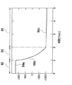
消去動作時に、消去対象であるワード線WLnに、すなわちコントロールゲートCGに、図37の電圧カーブ74が印加される。図37の横軸は時間をmsec単位で示し、縦軸は電圧をV(ボルト)単位で示す。図37には、このとき同時に、ワード線WLn+1に印加される電圧カーブ76と、消去対象であるセルトランジスタTCi,m−1,n,TCi,m,n, TCi,m+1,n のソースおよびドレインに印加される電圧カーブ78も合わせて示す。電圧カーブ76と、電圧カーブ78は、図に示すように、消去動作中、常に0Vである。電圧カーブ76を0Vとした理由は、消去が生じないようにするためにであり、電圧カーブ78を0Vとした理由は、コントロールゲートCGとフローティングゲートFGとの間に所定の電位差を生じさせるためである。
【0256】
本実施例では、電圧カーブ74が示すように、プリセット注入動作時にコントロールゲートCGにたとえば −13V(図37の矢印80)を、1msec(図37の矢印82)の間、印加して(この期間を以下では「プリセット期間」と呼ぶ。)、未書込フローティングゲートFGに電子を注入する。これにより、未書込フローティングゲートFG内の正電荷、すなわち正孔の数を減らす。
【0257】
その後、コントロールゲートCGに 13V(図37の矢印84)を、lmsec(図37の矢印86)の間印加し(この期間を以下では「第1の消去期間」と呼ぶ。)、続いて 11.5V(図37の矢印88)を、3msec(図37の矢印90)の間印加する(この期間を以下では「第2の消去期間」と呼ぶ。)。第1の消去期間と第2の消去期間を合わせた4msecの期間(矢印86, 90)が実質的な消去期間であり、この期間中に、プリセット期間に未書込フローティングゲートに注入された電子が消去されて、未書込フローティングゲートはプリセット注入動作開始時の状態に戻る。
【0258】
電圧カーブ74がコントロールゲートCGに印加されたときの、未書込フローティングゲートFG内の電荷数の変化を図38に示す。図38の縦軸は、フローティングゲートFG内に蓄積されている電子数を示し、「−」は、正孔が蓄積されていることを示す。横軸は時間をmsec単位で示す。
【0259】
図38の曲線92は、電荷数の変化を、コンピュータを用いてシミュレートしたものであり、プリセット期間82と、第1、第2の消去期間86, 90における電荷数の変化が曲線92a, 92b, 92c によりそれぞれ示されている。プリセット期間中に正孔の数が1200個から300個程度まで減少し、第1の消去期間に1100個程度まで増加し、第2の消去期間が終了するときには、正孔の数は1200個に戻っている。
【0260】
本発明においては、プリセット期間において未書込フローティングゲートFG内に電荷が注入され、消去動作が終了したときには、消去動作開始時の電荷数に実質的に戻っていることが重要である。
【0261】
電圧カーブ74がコントロールゲートCGに印加されたときの、書込済フローティングゲートFG内の電荷数の変化を図39に示す。図39の縦軸は、フローティングゲートFG内に蓄積されている電子数を示し、「−」は、正孔が蓄積されていることを示す。横軸は時間をmsec単位で示す。
【0262】
図39の曲線94は、電荷数の変化を、コンピュータを用いてシミュレートしたものであり、プリセット期間82と、第1、第2の消去期間86, 90の電荷数の変化が曲線94a, 94b, 94c によりそれぞれ示されている。プリセット期間82中は、電子の数は、1200個で安定しており、第1の消去期間中に電子がなくなり正孔の数が1100個程度まで増加し、第2の消去期間が終了するときには、正孔の数は1200個程度になっている。
【0263】
このように、“0”論理状態にある書込済フローティングゲートFGは、プリセツト注入によっても電荷の注入を受けず、一方、“1”論理状態にある未書込フローティングゲートFGは、一旦、電荷の注入を受ける。その後、いずれのフローティングゲートFGも消去操作を受けることとなる。ここで特徴的なことは、書込済フローティングゲートFGも、未書込フローティングゲートFGも最終的には、約−1200個の電子、すなわち1200個の正孔が充電された飽和状態で安定することである。
【0264】
なお、プリセット期間中に注入される電子数の下限値は、未書込フローティングゲートFGにおいて、飽和状態(すなわち1200個の正孔がある状態)よりも正孔がいくらかでも減少した状態になるような数であればよい。
【0265】
また注入される電子数の上限値に関しては、特に制限はなく、プリセット期間終了時に未書込フローティングゲートFG内の電子数が、書込済フローティングゲートFG内に当初あった電子数(+1,200)を越えるように、電子数を注入することも可能である。ただし、この電子数(+1,200)より少ないほうが、消去時間の短縮という点で望ましい。
【0266】
次に参考として、本実施例とは異なって消去動作において、電荷注入期間を設けないとした場合、消去動作時に消去対象であるワード線WLnに印加される電圧カーブ96を図40に示す。図40の横軸は時間をmsec単位で示し、縦軸は電圧をV(ボルト)単位で示す。
【0267】
図40には、ワード線WLn+1に印加される電圧カーブ76と、消去対象であるセルトランジスタTCi,m−1,n, TCi,m,n, TCi,m+1,n のソースおよびドレインに印加される電圧カーブ78も合わせて示す。電圧カーブ76と、電圧カーブ78は、図に示すように、消去動作中、常に0Vであり、図37と同じである。電圧カーブ96が示すように、消去動作時にコントロールゲートCGにたとえば +13V(図40の矢印98)を、5msecの間(図40の矢印100)、印加して消去動作を行なう。
【0268】
図37に戻って、ワード線WLnへ電圧カーブ74の電圧を印加するには、図33の電源部144が出力する電圧カーブ74に従った電圧をワードデコーダ140に入力し、ワードデコーダ140はワード線WLnを選択して、選択されたワード線WLnに当該電圧を印加する。このとき同時にワード線WLn+1に電圧カーブ76を印加するには、ワードデコーダ140によってワード線WLn+1を選択し、選択されたワード線WLn+1を接地することを同時に行なえばよい。
【0269】
消去対象のセルのソースおよびドレインへの0Vの電圧印加は、図33のビット線ゲート122が、接地すべきビット線BLm−1, BLm, BLm+1, BLm+2 に接続した仮想接地線VTを選択して、選択した仮想接地線VTを接地することにより行なう。
【0270】
消去対象であるセルトランジスタTCi,m−1,n, TCi,m,n, TCi,m+1,n と、消去対象ではないセルトランジスタTCi,m−1,n+1, TCi,m,n+1, TCi,m+1,n+1 は、いずれもバンクBNKi,m−1, BNKi,m, BNKi,m+1 に属するが、バンクBNKi,m−1, BNKi,m, BNKi,m+1 の選択は、既述のように行われる。
【0271】
以上述べたように、本実施例によれば、未書込フローティングゲートに対して過消去を繰り返すことができる。
【0272】
以上、本発明を詳細に説明したが、本発明は上記実施例に限定されない。本発明は、その主旨を逸脱しない範囲内で、適宜変形することができる。例えば、上記実施例では、一導電型としてp型を用い、反対導電型としてn型を用いたが、これに代えて、一導電型としてn型を用い、反対導電型としてp型を用いても良い。
【0273】
【発明の効果】
このように本発明によれば、書込みでは、ソース・ドレイン領域間に書き込み用の電位差を与えると共に、コントロールゲートに書き込み電圧を印加する。これにより、チャネルが、凸部の両側面と頂面の各表層に形成される。そして、頂面を流れるキャリアは、その進行方向を変える必要なくフローティングゲートに注入されるから、従来よりも書き込み電圧を低くすることができる。
【0274】
そして、読出しでは、ソース・ドレイン領域間に読出し用の電位差を与えるとともに、コントロールゲートに読出電圧を印加し、第1のドレイン電流Id1を流す。そして、上記読出し用の電位差を反転させることにより、第2のドレイン電流Id2を流す。フローティングゲートの電位は、ソース・ドレイン領域やコントロールゲートとの対向容量により、これらの部材の電位に引き付けられる。よって、上記ドレイン電流Id1、Id2を所望に大にしたり小にしたりすることができるから、電流ウインドウを所望に広げることができる。
【0275】
このように従来よりも書込電圧が低くかつ電流ウインドウが広い多値トランジスタが実現できるとともに、コントロールゲートと、ソース・ドレイン領域との間に、フローティングゲート中の蓄積電荷を消去するための消去電圧を印加することにより、コントロールゲートまたはソース・ドレイン領域に蓄積電荷を引き抜いて、フローティングゲートに蓄積された電荷を消去できる。
【0276】
また本発明によれば、過消去させることにより、単純な構造を有しつつ、書込効率を大きくして書込速度を向上させた半導体装置を提供することができる。
【0277】
また、本発明によれば、消去の際、書込みがなされているメモリと書込みが行われていないメモリを確認してその消去条件を切り替えるための確認ステップが不要になり、このステップに要する時間が短縮できる。
【0278】
さらに、本発明によれば、すべてのメモリに蓄積された電荷に対して実質的に零レベル以下(反対電荷が充電される状態)にまで過消去し、さらにその反対電荷がほぼ飽和するレベルまで過消去を行なうことにより、消去後のメモリを安定した電荷喪失状態(電子欠乏状態、正孔蓄積状態)とすることができ、安定した書込み、読出しおよび消去動作を実現することができる。
【図面の簡単な説明】
【図1】本発明の実施例に係る半導体メモリの切り欠き斜視図である。
【図2】本発明の実施例に係る半導体メモリが備えるセルトランジスタの拡大断面図である。
【図3】本発明の実施例に係る半導体メモリが備えるセルトランジスタの等価回路を模式的に表した図である。
【図4】本発明の実施例に係る半導体メモリが備えるセルトランジスタへの書込動作について示す断面図である。
【図5】本発明の実施例に係る半導体メモリが備えるセルトランジスタにおいて、凸部の頂面に高抵抗領域を設けた場合の断面図である。
【図6】本発明の実施例に係る半導体メモリが備えるセルトランジスタが達成し得る4値状態を示す断面図である。
【図7】本発明の実施例に係る半導体メモリが備えるセルトランジスタの読出動作について示す断面図である。
【図8】本発明の実施例に係る半導体メモリが備えるセルトランジスタにおいて、“(1、0)”状態を読み出す場合の断面図である。
【図9】フローティングゲートに注入された電子の消去方法の一例を示す断面図である。
【図10】本発明の実施例に係る半導体メモリが備えるセルトランジスタにおいて、フローティングゲートに注入された電子の消去方法を示す断面図である。
【図11】本発明の実施例に係る半導体メモリが備えるセルトランジスタにおいて、トンネル絶縁膜に繋がる厚膜の選択酸化膜を設けた場合の断面図である。
【図12】本発明の実施例に係る半導体メモリ全体の回路構成図である。
【図13】本発明の実施例に係る半導体メモリの製造方法について示す切り欠き斜視図(その1)である。
【図14】本発明の実施例に係る半導体メモリの製造方法について示す切り欠き斜視図(その2)である。
【図15】本発明の実施例に係る半導体メモリの製造方法について示す切り欠き斜視図(その3)である。
【図16】本発明の実施例に係る半導体メモリの製造方法について示す切り欠き斜視図(その4)である。
【図17】本発明の実施例に係る半導体メモリの製造方法について示す切り欠き斜視図(その5)である。
【図18】本発明の実施例に係る半導体メモリの製造方法について示す切り欠き斜視図(その6)である。
【図19】本発明の実施例に係る半導体メモリの製造方法について示す切り欠き斜視図(その7)である。
【図20】本発明の実施例に係る半導体メモリの製造方法について示す切り欠き斜視図(その8)である。
【図21】本発明の実施例に係る半導体メモリの製造方法について示す切り欠き斜視図(その9)である。
【図22】本発明の実施例に係る半導体メモリの製造方法について示す切り欠き斜視図(その10)である。
【図23】本発明の実施例に係る半導体メモリの製造方法について示す切り欠き斜視図(その11)である。
【図24】本発明の実施例に係る半導体メモリの製造方法について示す切り欠き斜視図(その12)である。
【図25】本発明の実施例において、ソース・ドレイン領域を凸部から後退させた場合の断面図である。
【図26】従来例に係る多値セルトランジスタの断面図である。
【図27】従来例に係る多値セルトランジスタへの書込動作を示すための断面図である。
【図28】従来例に係る多値セルトランジスタが達成し得る4値状態の断面図である。
【図29】従来例に係る多値セルトランジスタがバンド間トンネル耐性に乏しいことを説明するための断面図である。
【図30】本発明の実施例に係る半導体メモリが備えるセルトランジスタにおいて、凸部の基端部のボロン濃度を高くした場合の断面図である。
【図31】本発明の実施例に係る半導体メモリの製造方法において、pウエルの表面からの深さと、その深さでのボロン濃度との関係を示すグラフである。
【図32】本発明の半導体メモリの別の実施例における回路構成のうち、セルトタンジスタに関する部分の機能回路図である。
【図33】本発明の半導体メモリの別の実施例の構成を示す機能ブロック図である。
【図34】ビット線デコーダの一実施例を示す機能ブロック図である。
【図35】消去動作時にフローティングゲート内の電荷が減少するようすを例示するグラフである。
【図36】図32の一部を取り出して示す機能回路図である。
【図37】本発明の半導体メモリのさらに別の実施例における過消去動作での電圧プロファイルを示す図である。
【図38】図37に示す電圧を印加された未書込フローティングゲート内の電荷数の変化を示す図である。
【図39】図37に示す電圧を印加された書込済フローティングゲート内の電荷数の変化を示す図である。
【図40】電荷注入動作を行なわない場合の過消去動作での電圧プロファイルを参考として示す図である。
【符号の説明】
1、TC セルトランジスタ
2、12 p型シリコン基板
3、8、BL1〜BL4 ソース・ドレイン領域
4、6、26、29 シリコン酸化膜
5、25、27、30 シリコン窒化膜
7、CG コントロールゲート
12a p型エピタキシャル層
12b p+基板
13 pウエル
13a 凸部
13b 凸部の側面
13c 凸部の頂面
13d 反転層
13e 高抵抗領域
15a トンネル絶縁膜
15b インターポリ絶縁膜
15c ゲート絶縁膜
17 n型領域
18 シリコン熱酸化膜
20、24、35、39、45 フォトレジスト
21 nウエル
23 pウエル
28 トレンチ
30a 長穴
31 犠牲シリコン酸化膜
32 リセス
33 n+領域
34 選択酸化膜
36 WSi膜
37 ポリシリコン膜
38 キャップ膜
40 素子分離領域
41 ゲート電極
42 コラムデコーダ
43 ロウデコーダ
44 メモリセルアレイ
FG1、FG2 フローティングゲート
WL1〜WL4 ワード線[0001]
TECHNICAL FIELD OF THE INVENTION
The present invention relates to a multi-level transistor, a semiconductor memory using the same, and a driving method of the multi-level transistor. More specifically, the present invention relates to a technique useful for multi-valued semiconductor memory.
[0002]
[Prior art]
2. Description of the Related Art A non-volatile memory such as an EEPROM (Electrically Erasable Programmable Read Only Memory) is mounted on a mobile phone or the like and is now widely used. Normally, an EEPROM can write only one bit of information in one cell transistor. However, in order to reduce the size of the device, it is preferable that the cell transistor be multi-valued and two or more bits can be written in one cell transistor.
[0003]
FIG. 26 shows an example of this multilevel technique. FIG. 26 is a cross-sectional view of a multi-level cell transistor according to a conventional example (for this multi-level technology, see, for example, Patent Document 1).
[0004]
In FIG. 26, the
[0005]
In this type of cell transistor, in the n-type source /
[0006]
To write data into the
[0007]
As a result, electrons are accelerated by the electric field between the source /
[0008]
If the same is done by exchanging the source / drain voltage, as shown in FIG. 27B, the electrons are localized in a portion (referred to as a left bit) in the
[0009]
FIGS. 28A to 28D show quaternary states that can be achieved by the
[0010]
In order for the hot electrons to be injected into the
[0011]
However, hot electrons lose energy when they collide with phonons in the
[0012]
The high voltage is supplied by a high breakdown voltage transistor in a decoder circuit (not shown), but the high breakdown voltage transistor cannot be miniaturized. This is because, when miniaturized, there arises an inconvenience that the source / drain of the high breakdown voltage transistor punches through. Therefore, this writing method cannot reduce the chip size of the entire EEPROM including the decoder circuit.
[0013]
On the other hand, reading is performed by measuring two types of drain currents by exchanging applied voltages to the source /
[0014]
In the “(0, 0)” state (see FIG. 28D), since electrons are localized in both bits, the potential of the
[0015]
In the “(1, 1)” state (see FIG. 28A), since there is no electron in both bits, the potential of the
[0016]
On the other hand, in each of the states of “(1, 0)” and “(0, 1)” (see FIGS. 28B and 28C), since the electrons are localized only in one bit, the
[0017]
Therefore, "(1, 0)" and "(0, 1)" are distinguished by determining which of the two types of drain current is larger (or smaller) than the reference current. I can do it.
[0018]
However, this reading method is not preferable in reading “(1, 0)” or “(0, 1)” because the current window of the drain current is small. The current window refers to a difference between two types of drain current values measured by replacing the applied voltage of the source /
[0019]
The current window is desirably large when electrons are firmly localized at the right end (or left end) of the
[0020]
However, in the
[0021]
Further, the
[0022]
In this state, the potential difference ΔV between the
[0023]
In addition, since the potential difference ΔV is large, the edge of the
[0024]
[Patent Document 1]
U.S. Patent No. 6,011,725.
[0025]
[Problems to be solved by the invention]
SUMMARY OF THE INVENTION The present invention has been made in view of the problems of the conventional example. In a multi-valued transistor having a lower writing voltage and a wider current window than in the related art and a semiconductor memory using the same, the charge stored in the floating gate is high. It is an object of the present invention to provide a method for driving a multi-valued transistor while enabling erased charges.
[0026]
By the way, there are the following problems with nonvolatile memories such as EEPROM #. The EEPROM is widely used by being mounted on a mobile phone or the like. In the memory, it is generally most important that the unit cost per bit is low, and therefore, it is necessary that the memory cell be configured with a simple structure.
[0027]
On the other hand, increasing the writing speed in these memories is of great interest. For example, it has been considered to download music data from a terminal installed in a retail store such as a convenience store. In that case, it is desired that music data corresponding to one compact disk (CD) can be downloaded in about several seconds.
[0028]
To increase the write speed, reducing the write current is considered as one solution. This is because, when the write current is reduced, writing can be performed in parallel on the memory cells of a plurality of bits, and the writing speed can be improved.
[0029]
As a conventional technique for reducing the write current, for example, T.I. Kobayashi et al., "A Giga-Scale Assist-Gate (AG) -AND-Type Flash Memory Cell with 20-MB / s Programming Throughput for Content-Downloading Applications", International ELECTRON DEVICES Meeting (IEDM) 2001, Washington, DC, December 2}-{5, {2001,}. 2.2. There is one disclosed on page 2.2.4. According to this technique, a floating gate is provided above a channel region of a MOS semiconductor, a control gate is further provided above the floating gate, and an auxiliary gate is provided without providing a floating gate in a part of the upper portion of the channel region. The auxiliary gate controls the accumulation (writing) of electric charges in the floating gate to enable a small write current.
[0030]
The above-described prior art has a problem in that an auxiliary gate needs to be provided, and the structure of the memory cell is complicated.
[0031]
Another object of the present invention is to solve such a disadvantage of the prior art and to provide a transistor having a simple structure and improved writing speed.
[0032]
[Means for Solving the Problems]
An object of the present invention is to provide a first conductivity type semiconductor substrate provided with a convex portion having a pair of opposed side surfaces, a first insulating film formed on a top surface of the convex portion, A pair of opposite conductivity type source / drain regions formed on the surface of the semiconductor substrate sandwiching the portion, a second insulating film covering the side surface of the convex portion and the source / drain region, and provided on each side surface of the convex portion A pair of floating gates facing the side surface and the source / drain region with the second insulating film interposed therebetween, a third insulating film formed on each floating gate, and a third insulating film interposed therebetween. A control gate opposed to the floating gate and opposed to the top surface of the projection via the first insulating film, wherein the second and third insulating films have a capacitance higher than that of the first insulating film; Is formed so that the An erase voltage is applied between the gate and the source / drain region to erase the accumulated charge in the floating gate, an erase current flows toward the control gate or the source / drain region, and the accumulated charge is erased. The problem is solved by a transistor characterized in that:
[0033]
Alternatively, according to the second invention, a one-conductivity-type semiconductor substrate provided with a convex portion having a pair of opposed side surfaces, a first insulating film formed on a top surface of the convex portion, and the convex portion interposed therebetween. A pair of opposite conductivity type source / drain regions formed on the surface of the semiconductor substrate, a second insulating film covering the side surfaces of the protrusions and the source / drain regions, and a second insulating film provided on each side surface of the protrusions; A pair of floating gates facing the side surface and the source / drain regions via the insulating film, a third insulating film formed on each floating gate, and facing each floating gate via the third insulating film. And a control gate facing the top surface of the convex portion via the first insulating film, and the on / off state of the channel region facing the control gate is controlled by the control gate facing the top surface of the convex portion. Controlled An erasing voltage is applied between the control gate and the source / drain region to over-erase the charge stored in the floating gate, and the charge stored in the floating gate becomes substantially 0 or less. Thus, the problem is solved by a transistor characterized in that the charge stored in the floating gate is over-erased.
[0034]
Alternatively, a third aspect of the present invention includes a pair of opposite conductivity type source / drain regions formed in a surface layer of a semiconductor substrate of one conductivity type, a floating gate, and a control gate, and accumulating charges in the floating gate. It is possible to store data, and in a transistor in which a floating gate is provided so as to face only a part of a channel region between source / drain regions, a floating gate is provided between a control gate and a source / drain region. In the meantime, an erasing voltage for over-erasing the accumulated charge in the floating gate is applied, and the over-erasing is performed so that the charge accumulated in the floating gate becomes substantially 0 or less. Solved by transistors.
[0035]
Alternatively, in the transistor according to the second invention or the third invention, which is the fourth invention, writing to or reading from the floating gate is performed after overerasing. I do.
[0036]
Alternatively, in the transistor according to any one of the second to fourth inventions, which is the fifth invention, over-erasing is performed by maintaining a period for applying an erasing voltage to the control gate for a predetermined time. The problem is solved by a transistor characterized in that:
[0037]
Alternatively, in the transistor according to any one of the second invention to the fourth invention, which is the sixth invention, the electric charge accumulated in the floating gate is erased using a Fowler-Nordheim current, and The problem is solved by a transistor characterized in that charges accumulated in the floating gate are overerased until the value of the current becomes smaller than a predetermined value.
[0038]
Alternatively, in the transistor according to any one of the second invention to the sixth invention, which is the seventh invention, at least one of the floating gates to which data is not written among floating gates to be erased. The problem is solved by a transistor characterized in that a charge injection operation for injecting charges is performed.
[0039]
Alternatively, in the transistor according to any one of the second to seventh aspects of the present invention, writing of data to the floating gate is performed using a minimum write voltage value among writable write voltage values. The problem is solved by a transistor characterized in that the operation is performed using the second write voltage near the voltage value.
[0040]
Alternatively, a ninth invention, a semiconductor memory in which a plurality of transistors according to any one of the first invention to the eighth invention are arranged in a column direction and a row direction.
[0041]
Alternatively, in the transistor according to the ninth aspect, which is the tenth aspect, the cell transistors adjacent in the column direction have a common source / drain region, and the cell transistors adjacent in the row direction share a control gate. In addition, the problem is solved by a semiconductor memory characterized by sharing a source / drain region between cell transistors.
[0042]
Alternatively, in the eleventh aspect, a one-conductivity-type semiconductor substrate provided with a convex portion having a pair of opposed side surfaces, a first insulating film formed on a top surface of the convex portion, and the convex portion interposed therebetween. A pair of opposite conductivity type source / drain regions formed on the surface of the semiconductor substrate, a second insulating film covering the side surfaces of the protrusions and the source / drain regions, and a second insulating film provided on each side surface of the protrusions; A pair of floating gates facing the side surface and the source / drain regions via the insulating film, a third insulating film formed on each floating gate, and each floating gate via the third insulating film. A control gate opposed to the top surface of the projection with the first insulating film interposed therebetween, and the second and third insulating films have a larger capacitance than the first insulating film. In the driving method of the transistor that is formed as Thus, an erasing voltage for erasing stored charges in the floating gate is applied between the control gate and the source / drain region, and an erasing current is caused to flow toward the control gate or the source / drain region. The problem is solved by a transistor driving method including an erasing step of erasing charges.
[0043]
Alternatively, a twelfth invention, a one-conductivity-type semiconductor substrate provided with a convex portion having a pair of opposed side surfaces, a first insulating film formed on the top surface of the convex portion, and the first conductive film sandwiching the convex portion A pair of opposite conductivity type source / drain regions formed on the surface of the semiconductor substrate, a second insulating film covering the side surfaces of the protrusions and the source / drain regions, and a second insulating film provided on each side surface of the protrusions; A pair of floating gates facing the side surface and the source / drain regions via the insulating film, a third insulating film formed on each floating gate, and facing each floating gate via the third insulating film. And a control gate having a control gate opposed to the top surface of the projection via the first insulating film, wherein the control gate is opposed to the control gate by the control gate opposed to the top surface of the projection. Cha Controlling the on / off state of the floating gate, applying an erasing voltage between the control gate and the source / drain region for over-erasing the stored charge in the floating gate, Over-erasing the accumulated charge in the floating gate so that the accumulated charge is substantially zero or less.
[0044]
Next, the operation of the present invention will be described. According to the first and eleventh aspects, the channel is formed in a region other than the region connecting the source / drain regions linearly, that is, on one side → the top surface → the other side of the projection. Thus, the channel length can be increased with a small occupation area, and the size of the transistor can be reduced.
[0045]
In addition, since each side faces the floating gate, the floating gate is positioned in the traveling direction of the carrier flowing on the top surface. Therefore, at the time of writing, in order for carriers to be injected into the floating gate, it is not necessary to change the traveling direction of the carriers as in the related art, so that the acceleration voltage for accelerating the carriers can be reduced. Therefore, in the present invention, the write voltage can be made lower than in the prior art.
[0046]
Further, according to the above configuration, punch-through of the source / drain region can be prevented. As a result, even if the read voltage is relatively high, a large read signal can be obtained without causing punch-through. Furthermore, as a result of preventing punch-through, the gap between the source and drain of the cell transistor can be further reduced, and further miniaturization can be achieved.
[0047]
In addition, in the present invention, two floating gates are provided, and electrons are independently present in each floating gate. Therefore, even when miniaturizing a transistor, it is clear which of the floating gates has electrons, There is no ambiguity as to which bit the electron is localized as in the conventional example.
[0048]
Further, when the transistor is in a non-selected state, even if various potentials are applied to the source / drain regions to select another transistor connected to the transistor, the floating gate is not connected to the source / drain region. Thereby, it is attracted to the potential side of the source / drain region.
[0049]
Therefore, the potential difference between the floating gate and the source / drain region is reduced, so that no high electric field is applied to the second insulating film between them. Therefore, a tunnel current hardly flows through the second insulating film, so that the second insulating film is prevented from being deteriorated.
[0050]
In addition, since the potential difference is reduced as described above, the generation of hot holes due to a high electric field at the pn junction between the source / drain region and the substrate is suppressed, and the hot holes deteriorate the second insulating film. Is also prevented. In other words, the present invention improves the inter-band tunnel resistance.
[0051]
The reading of the present invention will be described. In the read operation, first, a read potential is applied between the source / drain regions, a read voltage is applied to the control gate, and the first drain current Id 1Flow.
[0052]
At this time, the potential of the floating gate is determined by the capacitive coupling with the source / drain region and the control gate, in addition to the potential drop due to the injected charge.
[0053]
For example, when a positive potential is applied to the control gate as a read voltage, the floating gate is attracted to the positive potential by capacitive coupling. In particular, when the floating gate is on the higher potential side of the pair of source / drain regions, the potential is also attracted to the positive potential side by capacitive coupling with the source / drain regions. Therefore, even when electrons (charges) are injected into the floating gate, lowering of the potential of the floating gate due to the electrons is suppressed, and the channel near the floating gate becomes relatively large. Therefore, even if electrons are injected into the floating gate, the first drain Id 1Will be as large as desired.
[0054]
Next, the potential difference for reading is inverted, and the read voltage is applied to the control gate, thereby causing the second drain current Id 2Flow.
[0055]
Since the potential difference for reading is inverted, the floating gate into which electrons have been injected faces the source / drain region on the lower potential side. Therefore, the potential of the floating gate is lowered not only by the potential drop due to the injected electrons, but also by the capacitance opposed to the source / drain regions. Therefore, the channel resistance near the floating gate becomes large, so that the second drain current Id 2Is desirably small.
[0056]
Thus, in the present invention, each drain current Id 1, Id 2Can be made as large or small as desired, so that their difference (current window) is widened as desired.
[0057]
As described above, it is possible to realize a multi-valued transistor having a lower write voltage and a wider current window than the conventional one, and to erase accumulated charges in the floating gate between the control gate and the source / drain regions. By applying the erasing voltage, the charges accumulated in the control gate or the source / drain regions can be extracted, and the charges accumulated in the floating gate can be erased.
[0058]
According to the second, third, and twelfth aspects, in the transistor, over-erasing is possible when the floating gate is provided only in a part of the channel region between the two opposite conductivity type regions. And that the over-erasing improves the writing efficiency. The erasing means applies an erasing voltage to at least the control gate to over-erase the charge accumulated in the floating gate. Thereafter, when normal writing is performed, writing can be performed with a small write current because the writing efficiency is improved.
[0059]
Here, the over-erase refers to a state in which electrons stored in the floating gate are extracted from the floating gate, and the number of electrons stored in the floating gate is substantially “0” or less. In this state, the threshold voltage of the memory cell is about 0 V or less than 0 V. Here, that the number of electrons is smaller than “0” means that positive charges (holes) are accumulated in the floating gate.
[0060]
The reason why the over-erasing improves the writing efficiency is that the voltage of the floating gate is increased by the over-erasing, and the potential difference from the channel region is increased.
[0061]
According to the fourth aspect, since writing or reading is performed after over-erasing, the writing efficiency is improved and the current window is widened. The write efficiency is improved because the overerased floating gate has a high potential (when the stored charge is an electron) due to overerased, which facilitates carrier injection. is there.
[0062]
The reason for the widening of the current window is that the potential of the over-erased floating gate is high (when the stored charge is an electron) because of over-erasing, and the difference from the potential of the floating gate in which the charge is stored is different. Because it is expanding.
[0063]
According to the fifth aspect, over-erasing can be performed by maintaining a period for applying the erasing voltage to the control gate for a predetermined time. The predetermined time can be set, for example, to a time during which electrons in the floating gate are surely overerased.
[0064]
According to the sixth aspect, the electric charge accumulated in the floating gate is erased using the Fowler-Nordheim {(Fowler-Nordheim)} current (hereinafter referred to as the FN current), and the value of the FN current becomes smaller than the predetermined value. Until the charge accumulated in the floating gate is over-erased.
[0065]
The erasing is performed by extracting electrons from the floating gate by the FN current. After the erasing starts, the FN current becomes a constant value when over-erasing proceeds to some extent, and the charge amount in the floating gate also becomes constant. In other words, a state where erasing is not performed any more is brought about. Therefore, for example, this constant value can be adopted as the predetermined value of the FN current.
[0066]
According to the seventh aspect, of the floating gates of cells to be erased, over-erasing is performed after performing a charge injection operation of injecting charges into a floating gate to which data is not written.
[0067]
The reason for performing the charge injection operation is as follows. For a floating gate in a “0” logic state in which data is not written (hereinafter, referred to as “unwritten floating gate”), over-erasing is repeatedly performed many times without performing charge injection. Then, the operation of forcibly extracting the charge (for example, electrons) from the unwritten floating gate is repeatedly performed. As a result, the unwritten floating gate that has been stable in the over-erased state, that is, the saturated state, becomes an electron deficient state (hereinafter, referred to as “excessively erased state”) beyond the saturated state, and the threshold voltage and the like change. there's a possibility that.
[0068]
If the charge injection operation is performed before the over-erase operation, the unwritten floating gate in which the data is not written continues when the over-erase operation is performed many times compared to when the charge injection operation is not performed. Is not repeated.
[0069]
The above-described charge injection operation may be performed as a preset injection operation of injecting charge into an unwritten floating gate among floating gates of a cell to be erased before applying an erasing voltage to the control gate. preferable.
[0070]
Further, in the transistor of the present invention, the charge injection operation may be performed by applying a charge injection voltage to the control gate.
[0071]
At this time, regardless of whether or not data is being written to the floating gate, that is, without considering whether or not the floating gate is an unwritten floating gate, a charge is applied to the cell to be erased. An injection voltage can be applied. For example, it is necessary to select the magnitude of the charge injection voltage and the application time so that the charge is injected into the unwritten floating gate, but the charge is not injected into the written floating gate. it can. By employing this method, it is not necessary to determine whether or not the floating gate is an unwritten floating gate, so that the erasing operation is simplified.
[0072]
According to the eighth aspect, the writing of data to the floating gate after erasing is performed using the second write voltage near the minimum voltage value among the writable write voltage values. In the present invention, the write efficiency is improved as compared with the prior art due to over-erasing, and the write efficiency is maximized when the writable write voltage value is the minimum voltage value. ing. Therefore, by performing writing with the minimum voltage value among the writable write voltage values, the write current can be minimized, and simultaneous writing to many memory cells becomes possible, and an effective write Loading speed is increased.
[0073]
According to the ninth and tenth aspects, the semiconductor memory in which a plurality of transistors are arranged in the column direction and the row direction, and the source / drain regions of the cell transistors adjacent in the column direction are common, and the transistors are arranged in the row direction. Since the adjacent memory cell transistors share a control gate and share the source / drain region between the memory cell transistors, a semiconductor memory in which the above-described transistors are integrated can be configured.
[0074]
BEST MODE FOR CARRYING OUT THE INVENTION
Next, embodiments of the present invention will be described in detail with reference to the accompanying drawings.
[0075]
(1) Device structure
FIG. 1 is a cutaway perspective view of the semiconductor memory according to the present embodiment. This
[0076]
In addition, a plurality of
[0077]
Each of the floating gates FG1, FG2 and the control gate CG is made of polysilicon. The control gates CG are integrated in the row direction and are formed in a plurality in the column direction, each of which functions as word lines WL1, WL2,.
[0078]
A
[0079]
FIG. 2 is an enlarged cross-sectional view of a cell transistor TC which is one feature of the present invention. A
[0080]
The
[0081]
The floating gates FG1, FG2 are provided on the respective side surfaces of the
[0082]
The
[0083]
In the above structure, the channel is formed three-dimensionally on each surface layer of both
[0084]
The p-type impurity concentration of the
[0085]
FIG. 3 is a diagram schematically showing an equivalent circuit of the cell transistor TC, and shows various capacitances. The meaning of each capacity is as follows.
・ CCG: Opposing capacitance between the control gate CG and the
・ CCF1(CCF2): Capacitance between control gate CG and floating gate FG1 (FG2).
・ CFG1(CFG2)... Opposing capacitance between the floating gate FG1 (FG2) and the
・ CFS(CFD): Capacitance of the floating gate FG1 (FG2) and the source / drain region BL1 (BL2).
[0086]
Please refer to FIG. 1 again. A plurality of cell transistors TC, TC,... Are arranged in the column direction and the row direction. Cell transistors adjacent in the column direction (for example, TCaAnd TCbAre common to the source / drain regions BL3 and BL4, and are electrically isolated by the
[0087]
(2) Driving method
Next, a method of driving the above-described cell transistor TC will be described.
[0088]
I) Write operation
The write operation will be described with reference to FIG. FIG. 4 is a cross-sectional view showing a write operation to the cell transistor TC. As described above, the pair of floating gates FG1 and FG2 are provided on both sides of the
[0089]
For example, to inject electrons into the right floating gate FG2, as shown in FIG.G(For example, 2.2 V). The voltage V is applied to the source / drain region BL2 on the side where electrons are injected.DD(For example, 6 V). The
[0090]
According to this, since a positive potential is applied to the control gate CG, an
[0091]
Therefore, carriers (electrons in this embodiment) flow along the path indicated by the arrow in FIG. In particular, note the electrons flowing on the
[0092]
Moreover, by providing the n-
[0093]
The above advantages can be obtained even if the channel resistance at the
[0094]
The structure for increasing the channel resistance is not limited to the above, and the structure shown in FIG. 5 may be employed. In this structure, a high resistance region (one conductivity type impurity region) 13e is provided on the
[0095]
As shown in FIG. 4 or FIG. 5, when the channel resistance at the
[0096]
Stated above, the write voltage VGIi) increasing the capacitance of the tunnel insulating film and raising the floating gate by the drain voltage, iii) increasing the thickness of the
[0097]
In FIG. 4, electrons are injected only into the right floating gate FG2. However, in order to inject electrons into the left floating gate FG1, the voltages of the source / drain regions BL1 and BL2 may be exchanged. Therefore, in the present invention, four states shown in FIGS. 6A to 6D are obtained.
[0098]
FIG. 6A shows a “(1, 1)” state in which electrons are not injected into both floating gates FG1 and FG2. FIGS. 6B and 6C show the “(1, 0)” and “(0, 1)” states in which electrons are injected into only one of the floating gates FG1 and FG2. FIG. 6D shows a “(0, 0)” state in which electrons are injected into both floating gates FG1 and FG2. To obtain this state, for example, after injecting electrons into the right floating gate FG2, electrons may be injected into the left floating gate FG1. Thus, in this embodiment, 2-bit data “(0, 0)” to “(1, 1)” can be written in one cell transistor TC.
[0099]
In the present embodiment, two floating gates FG1 and FG2 are provided, and electrons are independently present in each of the floating gates FG1 and FG2. Therefore, even when the cell is reduced, which one of the floating gates FG1 and FG2 is present. Is clear, and it is not unclear which bit the electron is localized as in the conventional example.
[0100]
II) Read operation
Next, the read operation will be described with reference to FIGS. To read data, first, as shown in FIG. 7A, a read voltage V is applied to the control gate CG.G(For example, 2.2 V). The voltage V is applied to one of the source / drain regions BL2.DD(For example, 1.6 V), and the other source / drain region BL1 and the
[0101]
With such a potential distribution, the control gate CG has a positive potential, so that the
[0102]
Next, as shown in FIG.G(That is, 2.2 V), the voltages of the source / drain regions BL1 and BL2 are exchanged. In this case, the potential difference between the source / drain regions BL1 and BL2 is inverted, so that the second drain current Id2Flows.
[0103]
In this embodiment, two types of drain currents I are set by replacing the voltages of the source / drain regions BL1 and BL2 as described above.d1, Id2Is measured. Such a drain current Id1, Id2Is different depending on each of the quaternary states as described later. Therefore, a set of two types of drain current values (Id1, Id2) And each state are in one-to-one correspondence, so that which state is stored can be read. Next, the drain current value in each of the states “(1, 1)” to “(0, 0)” will be described.
[0104]
(I) "(1, 0)" state
FIGS. 8A and 8B are cross-sectional views when reading the “(1, 0)” state. In FIG. 8A, the voltage applied to each member is as shown in FIG. 7A, and the drain current Id1Flows. In the state of FIG. 8A, the potential of the right floating gate FG2 is lowered due to the injection of electrons. However, the potential of the floating gate FG2 is set to the opposite capacitance CCF2, CFDThereby, the potential is raised to the positive potential side of the control gate CG (2.2 V) and the source / drain BL2 (1.6 V).
[0105]
As a result, since the potential drop of the floating gate FG2 is suppressed, the channel resistance near the floating gate FG2 is not so large. Therefore, the drain current Id1Is relatively large.
[0106]
In particular, when the n-
[0107]
On the other hand, FIG. 8 (b) shows that the drain current Id2Is flowing. In this case, the potential of the right floating gate FG2 decreases due to the injected electrons. In addition, since the right source / drain region BL2 is grounded, the potential of the floating gate FG2 becomes the opposite capacitance C with the source / drain region BL2.FDIs pulled down to the ground side. Therefore, the potential of the floating gate FG2 becomes lower than that in the case of FIG. 8A, so that the channel resistance near the floating gate FG2 increases and the drain current Id2Is Id1Smaller than.
[0108]
In particular, when the n-
・ (Id1, Id2) = (Large, small)
Can be identified by This drain current Id1, Id2Is determined by a sense amplifier (not shown) by comparing with a reference current.
[0109]
In this embodiment, each drain current Id1, Id2Is the opposite capacitance CCF2, CFD, CFG2Accordingly, the size can be increased or decreased as desired as described above. Therefore, the difference (Id1-Id2) Can be increased as desired. Difference (Id1-Id2) Is a current window, and in this embodiment, the current window can be expanded as desired. Since the current window is wide, the drain current Id1, Id2And the reference current becomes wider, and the risk of erroneously recognizing the write data can be reduced.
[0110]
(Ii) "(0, 1)" state
In the “(0, 1)” state, on the contrary, electrons are injected into the left floating gate FG1. Therefore, each drain current Id1, Id2Is evaluated in the same manner as in the above discussion,
・ (Id1, Id2) = (Small, large)
It becomes.
[0111]
(Iii) "(1, 1)" state
In the “(1, 1)” state, no electrons are injected into any of the floating gates FG1, FG2. Therefore, the potential of each of the floating gates FG1, FG2 is not lowered by the electrons, so that Id1, Id2Both are great. Also, since this state is symmetrical, Id1And Id2There is no difference between
・ (Id1, Id2) = (Large, Large)
It becomes.
[0112]
(Iv) "(0, 0)" state
The “(0, 0)” state is symmetrical because electrons are injected into both floating gates FG1 and FG2. Therefore, Id1And Id2There is no difference between
・ (Id1, Id2) = (Small, small)
It becomes.
[0113]
In the read operation of the semiconductor memory of the present invention, after the logic state of "(0, $ 0)" to "(1, $ 1)" as described above is determined, reading may be performed based on this. The read operation can be performed as follows. In other words, in the read operation of the semiconductor memory of the present invention, after all, it depends on whether or not charges are accumulated in the floating gate opposite to the source / drain on the side to which the read voltage is not applied (ground side). The drain current value Id will change. Therefore, when a drain voltage is applied to one of the source and the drain, the charge accumulation state of the floating gate to which no voltage is applied can be independently detected only by detecting the drain current value obtained thereby. Yes, reading can be performed in this manner.
[0114]
III) Erase operation
Next, a method of erasing electrons injected into the floating gates FG1, FG2 will be described. In order to extract the stored electrons, a method of extracting the electrons to the source / drain regions BL1 and BL2 can be considered as shown in FIG. In this method, the control gate CG is grounded, and a high potential “H” (eg, 12 V) is applied to the source / drain regions BL1 and BL2. Here, the potential difference between the control gate CG and the source / drain regions BL1, BL2 can be set relatively. For example, -6V is applied to the control gate CG, and 6V is applied to the source / drain regions BL1, BL2. You may do so.
[0115]
As another method, as shown in FIG. 10, a high potential V is applied to the control gate CG.G(For example, 12 V) to ground the
[0116]
Further, in the potential distribution of FIG. 10, since the control gate CG has a higher potential than the protruding
[0117]
Therefore, since the potential of the floating gate FG1 (FG2) further decreases, the potential difference between the floating FG1 (FG2) and the
[0118]
In addition, since the potential of the floating gate FG1 (FG2) is attracted to the potential of the source / drain region BL1 (BL2) or the
[0119]
iv) When not selected
The above i) to iii) were all cases where the
[0120]
Even in a non-selected state, the bit line BL1 (see FIG. 3) is supplied with the voltage V for each operation to select another cell transistor TC.DDIs applied. In this case, the floating gate FG1 of the non-selected cell transistor TC is connected to the large opposing capacitance C with the bit line BL1.FSThereby, the potential of the bit line BL1 is attracted. Therefore, the potential difference between the floating gate FG1 and the source / drain region BL1 is reduced, so that the
[0121]
In addition, since the potential difference is reduced as described above, generation of a hot hole due to a high electric field at the pn junction between the source / drain region BL1 and the
[0122]
Here, in order to obtain the advantages of i) to iv) at the time of driving, the opposing capacitance C between the floating gate FG1 (FG2) and the source / drain region BL1 (BL2).Fs(CFDNote that) plays an important role. In the present embodiment, the floating gate FG1 (FG2) is covered on the source / drain region BL1 (BL2) to reduce the distance between the floating gates FG1 and FG2 and to reduce the size of the device.FD, CFSTo make it easier to obtain the advantages described above.
[0123]
The facing area between the floating gate FG1 (FG2) and the source / drain region BL1 (BL2) is not limited. The above-mentioned advantages are more easily obtained as the facing area is larger, but it is possible to obtain the same even if the facing area is smaller. Therefore, as shown in FIG. 25, even if the source / drain region BL1 (BL2) is retreated from the
[0124]
(3) Countermeasures against punch-through and threshold voltage VthStabilization
By the way, if punch-through between the source / drain BL1 and BL2 poses a problem during the above-mentioned write or read operation, it is preferable to adopt the structure shown in FIG. The graph in FIG. 30 shows the relationship between the depth of the
[0125]
With the above structure, the concentration of the p-type impurity in the channel near the n-type source / drain BL1 and BL2 is increased. Therefore, the channel is a region that linearly connects the n-type source / drain BL1 and BL2 ( (regions close to the n-type source / drain BL1 and BL2), that is, on the surface layers of the side surfaces 13b and 13b and the
[0126]
By the way, the threshold voltage V of the cell transistor TCthIs greatly affected by the impurity concentration on the side surfaces 13b of the base end portion. Therefore, when the boron concentration is increased at the base end as described above, the threshold voltage V of the cell transistor TC is increased.thWill be higher.
[0127]
However, when the n-
[0128]
Further, as described above, the threshold voltage VthIs sensitive to the impurity concentration at the base end,thIn order to stabilize, it is preferable that the impurity concentration does not fluctuate much at the base end. Therefore, it is preferable that the boron concentration in the
[0129]
(4) Measures against leakage current between control gate and bit line
In the present embodiment, as shown in FIG. 11, the control gate CG and the bit line BL2 face each other in the portion A between the cell transistors TC adjacent in the row direction. Therefore, it is conceivable that a leak current flows between the control gate CG and the bit line BL2 in the portion A during various operations.
[0130]
If this point is a concern, the
[0131]
When the insulator is buried between the control gate CG and the bit lines BL1 and # BL2, the floating gates FG1 and # FG2 only face the control gate CG via the interpoly
[0132]
(5) Overall circuit configuration
FIG. 12 shows a circuit configuration of the entire embodiment. As shown in FIG. 12, the
[0133]
The gate voltage V is applied to the selected word lines WL1 to WL4.GIs supplied. Gate voltage VGIs switched as desired during each of the write / read / erase operations, and a voltage for each operation is applied. As described above, the gate voltage VGIs 2.2 V at the time of writing, 2.2 V at the time of reading, and 12 V at the time of erasing. On the other hand, the word lines WL1 to WL4 may be in a floating state when not selected.
[0134]
On the other hand, the bit lines BL1 to BL3 of the respective cell transistors TC, TC,... Are connected to the output of the column decoder 42. Column decoder 42 decodes column decode signal CDC of a predetermined bit, and selects bit lines BL1 to BL3 corresponding to signal CDC.
[0135]
The voltage V is applied to the selected bit lines BL1 to BL3.DDIs supplied. Voltage VDDIs switched as desired during each of the write / read / erase operations, and a voltage for each operation is applied. As described above, the voltage VDDIs ground at 6 V during writing, ground or 1.6 V at reading, and ground at erasing. On the other hand, the bit lines BL1 to BL3 may be in a floating state when not selected. An arbitrary cell transistor TC is selected by a selected bit line BLi and a selected word line WLj, and each operation of writing / reading / erasing is performed.
[0136]
(7) Manufacturing process
Next, a method for manufacturing a semiconductor memory according to the present embodiment will be described with reference to FIGS. First, as shown in FIG. 13A, a p-
[0137]
Next, as shown in FIG. 13B, a
[0138]
In this embodiment, the manufacturing process of the cell transistor can be performed simultaneously with the manufacturing process of the CMOS transistor. Hereinafter, not only a cell transistor but also a manufacturing process of a CMOS transistor will be described. In the drawing, a CMOS transistor portion indicates a portion where a CMOS transistor is formed later. The cell transistor portion indicates a portion where the cell transistor is formed. The above-described
[0139]
Subsequently, as shown in FIG. 14A, a
[0140]
Next, as shown in FIG. 14B, a
[0141]
Next, as shown in FIG. 15A, a
[0142]
Next, as shown in FIG. 15B, a
[0143]
・ First time: Ion species: BF2
Acceleration energy: 15 (KeV)
Dose amount: 5.0 × 10¹¹(Cm-2)
・ Second time: Ion species: BF2
Acceleration energy: 45 (KeV)
Dose amount: 5.0 × 10¹¹(Cm-2)
・ 3rd time ・ ・ ・ Ion species: B (boron)
Acceleration energy: 20 (KeV)
Dose amount: 6.0 × 10¹²(Cm-2)
-4th time: Ion species: B (boron)
Acceleration energy: 40 (KeV)
Dose amount: 5.0 × 10¹²(Cm-2)
Dose amount: 5.0 × 10¹²(Cm-2)
By the four ion implantations described above, the p-well 13 shows a boron concentration distribution as shown in FIG. FIG. 31 is a graph showing the relationship between the depth from the surface of the p-well 13 and the boron concentration at that depth.
[0144]
In the figure, the net boron concentration is represented by an envelope (solid line) of the boron concentration (dotted line) for each time. As is clear from this, a peak (a thick line portion) is formed in the boron concentration distribution. Preferably, the peak is formed flat by appropriately adjusting the ion implantation conditions, and the flat portion is made to exist as widely as possible in the depth direction. The reason will be clear from FIG. 16B described later.
[0145]
Next, as shown in FIG. 16A, the silicon thermal oxide film 18 (see FIG. 15B) is removed by etching while leaving the previous
[0146]
On this
[0147]
Next, as shown in FIG. 16B, a
[0148]
The
[0149]
As a result, a
[0150]
Returning to FIG. 16B again, the size of the
[0151]
Subsequently, as shown in FIG. 17A, a silicon oxide film 29 (having a thickness of about 20 nm) is formed on the entire exposed surface. The
[0152]
Thereafter, bit lines BL1, BL2,... Are formed at the bottoms of the
[0153]
Ion species: As (arsenic)
Acceleration energy: 15 (KeV)
Dose amount: 2.0 × 10¹⁴(Cm-2)
After completing the ion implantation, the
[0154]
Then, as shown in FIG. 18A, arsenic is ion-implanted into both
[0155]
Ion species: As (arsenic)
Acceleration energy: 10 (KeV)
Dose amount: 5.0 × 10¹¹(Cm-2)
At the time of ion implantation, since the thin silicon oxide film 29 (see FIG. 17B) remains on the
[0156]
By the way, the surface layer of the
[0157]
In view of this point, in the present embodiment, as shown in FIG. 18B, the sacrificial
[0158]
Since the surfaces of the
[0159]
Subsequently, as shown in FIG. 19A, the
[0160]
Thereafter, arsenic is ion-implanted into the bit lines BL1, BL2,... Through the
[0161]
Ion species: As (arsenic)
Acceleration energy: 30 (KeV)
Dose amount: 3.0 × 10Fifteen(Cm-2)
19B, the
[0162]
Thereafter, as shown in FIG. 20A, the bottom and side surfaces of the
[0163]
In this embodiment, a plasma oxidation method is used to form a high-quality
[0164]
Krypton excited by microwaves is oxygen (O2) And a large amount of atomic oxygen O*Is generated. Atomic oxygen O*Easily penetrate into the surface layers of the
[0165]
After forming the
[0166]
Next, as shown in FIG. 21A, the
[0167]
Subsequently, as shown in FIG. 21B, a
[0168]
Next, as shown in FIG. 22A, after removing the
[0169]
Since the floating gates FG1 and FG2 are made of polysilicon, a large number of crystal grains having various plane orientations are formed on the surface thereof. As described above, even if the plane orientation varies, the above-described plasma oxidation method enables a silicon oxide film to be uniformly formed without depending on the plane orientation. Therefore, the thickness of the interpoly
[0170]
Subsequently, a structure shown in FIG. To obtain this structure, first, a polysilicon film is formed on the entire exposed surface. This polysilicon film will later become the control gate CG. The polysilicon film is doped with phosphorus (P) in advance by an in-situ process. Next, a
[0171]
By this step, a plurality of control gates CG, CG,... Formed integrally in the row direction are formed. At the same time, a
[0172]
Next, as shown in FIG. 23A, a
[0173]
Subsequently, as shown in FIG. 23B, using the
[0174]
Finally, as shown in FIG. 24, an
[0175]
To form the
・ Ion type: BF2
・ Acceleration energy: 20 (KeV)
・ Dose amount: 1.0 × 10¹³(Cm-2)
Thereafter, by removing the
[0176]
Next, another embodiment of the present invention will be described. This embodiment has one feature in over-erasing a memory cell. The present embodiment focuses on improving the writing efficiency and improving the writing speed by over-erasing the charges accumulated in the floating gate so as to be substantially 0 or less. .
[0177]
In this embodiment, since the floating gate is intended for a semiconductor memory provided only in a part of the channel region between the two opposite conductivity type regions, the floating of the floating gate is achieved by grounding the control gate. Current can be cut off in a channel region where a gate is not provided, and current can be prevented from flowing to a memory cell which is not selected at the time of reading or the like. That is, no current flows when the control gate of a memory cell not selected at the time of reading or the like is grounded. Further, there is an advantage that the over-erasing increases the current window margin (that is, the current difference between when the charge is stored in the floating gate and when the charge is not stored).
[0178]
In the present embodiment, over-erasing is performed by performing the above-described erasing operation on a memory cell to be erased for a time during which over-erasing occurs in the memory cell, for example, for 5 msec. After the elapse of this time, the erasing operation is saturated in the over-erased state of the floating gate, and a stable charge loss state (electron deficiency state, hole accumulation state) is reached. No more positive charges are stored in the gate.
[0179]
Next, the semiconductor memory according to the present embodiment will be specifically described. In the following description, components having the same functions as the components of the above-described embodiments will be denoted by the same reference numerals, and the description thereof will be partially omitted.
[0180]
A circuit configuration of the semiconductor memory according to the present embodiment will be described. FIG. 32 is a circuit configuration diagram of the
[0181]
Cell transistor TCi , M, pEach of the banks BNKi, m, And corresponds to TC described above with reference to FIG. Each bank BNKi, mRepresents n cell transistors TC arranged in (1 column) × (n rows)i , M, pConsists of Note that n represents a predetermined natural number, and the value is not particularly limited. Bank BNKi, mAre the cell transistors TC belonging to the bank.i , M, PRepresents a common row number and column number, respectively.
[0182]
In this circuit, while a normal flash memory selects a cell transistor by a combination of a word line and a bit line, first, an even-numbered bank group BNK in i row is selected.i, m(M = 0, 2, 4 ...) and the odd-numbered bank group BNKi, m(M = 1, 3, 5,...) To one of the selection lines SEi, SOiTo select the bit line BL from the bank group.m(M = 0, 1, 2,...) (More precisely, the bit line BLmVirtual ground line VT connected toK), Select one bank and then its bank BNKi, mOne of the cell transistors TCi , M, pTo the word line WLpUse to select. Hereinafter, this will be described in detail.
[0183]
Each bank BNKi, mHas a selection transistor STE for selecting it.i , M, @STOi , MAre connected one by one. Among them, the selection transistor STEi , MIs the bank BNK in the i rowi, mBank BNK whose column number is eveni, m(M = 0, 2, 4,...), And is hereinafter also referred to as an even-numbered bank selection transistor. Select transistor STEi , MSelect line SE to specifyiIs used. One selection line SEiHas all the select transistors STE arranged in the i row.i , M(M = 0, 1, 2,...) Are connected. Select line SEiSelect line SEiSelect transistors STE connected toi , M(M = 0, 1, 2,...) Is selected.
[0184]
Also, the selection transistor STOi, mIs the bank BNK in the i rowi, mOf which the column number is oddi, m(M = 1, 3, 5,...), And is hereinafter also referred to as an odd-numbered bank selection transistor. Select transistor STOi , MSelect line SOiIs used. One selection line SOiAll select transistors STO arranged in the i rowi , M(M = 0, 1, 2,...) Are connected. Select line SOiSelect line SOiSelect transistors STO connected toi , M(M = 0, 1, 2,...) Is selected.
[0185]
As shown in FIG.i, mHave their one source / drain connected in common every other column, and have their common connection nodes A, #D, #E connected to a virtual ground line VT.k(K = 0, 1, 2,...) Are connected.
[0186]
Odd bank selection transistor STOi, mIs the same, but the common connection point is an even-numbered bank selection transistor STE.i, mIs shifted by one column.
[0187]
In the figure, the symbol STEi-1 , M(M = O, 2,...) Is an even-numbered bank selection transistor for selecting an even-numbered bank from the (i-1) -th bank counted in the column direction. On the other hand, the code STOi + 1, m(M = 1,,...) Are odd-numbered bank selection transistors for selecting an odd-numbered bank from the (i + 1) -th bank counted in the column direction.
[0188]
Also, the virtual ground line VTk(K = 0, 1, 2,...) Are made of a metal such as aluminum in order to reduce the electric resistance. On the other hand, the bit line BLm(M = 0, 1, 2,...) Are made of a diffusion layer, and the electric resistance of the diffusion layer iskMuch higher than that of.
[0189]
The circuit operation is as follows. For example, at the time of reading, the cell transistor TC shown in FIG.i, m, 0(Here, m is assumed to be an even number). Cell transistor TCi, m, 0Is even bank BNKi, mBelongs to. Therefore, first, the even-numbered bank group BNKi, m(M = 0, 2, 4,...) To select even bank selection lines SEiTo a high level, and each even-numbered bank selection transistor STEi, m(M = 0, 1, 2,...) Are turned on. Other selection lines (SEr(R = 0, 1, 2, ..., i-1, i + 1, ...), SOr(R = 0, 1, 2,...)) Are all set to the low level, and all the transistors whose selection lines are connected to the gates are turned off.
[0190]
According to the voltage distribution described above, the even-numbered bank selection transistor STE in the ON statei, m, STEi, m + 1The bit line BLm, BLm + 1Is the virtual ground line VTk, VTk + 1Is electrically connected. Other even bank BNKi, m-2, @ BNKi, m + 4Similarly, the bit line connected to the virtual ground line is electrically connected to the virtual ground line.
[0191]
Next, the target cell transistor TCi, m, 0To select the bit line BLmVirtual ground line VT connected viakTo the ground level, and the bit line BLm + 1Virtual ground line VT connected viak +1, A low voltage VDD (= 1.6 V) is applied. The other virtual ground lines VT are kept open. In this way, first, the even bank groupi, m(M = 0, 2, 4,...) Is selected. Specifically, the setting of the virtual ground line VT is performed by the
[0192]
With these voltage values applied to the source / drain, as described with reference to FIG.i, m, 0First drain current Id1Flows. This first drain current Id1, The
[0193]
Next, the
[0194]
Thus, the cell transistor TCi, m, 0First drain current Id1And the second drain current Id2Is measured by the sense amplifier, and the cell transistor TCi, m, 0Which of the quaternary states "(0, $ 0)" to "(1, $ 1)" is stored is identified.
[0195]
According to this circuit configuration, the first drain current Id1Is a high-resistance bit line BL made of a diffusion layer.m, BLm + 1Not always flowing inside, but the target bank BNKi, mUntil it reaches a low resistance virtual ground line VGk + 1Flow through the target bank BNKi, mAfter reaching bit line BLm + 1Will flow through. Then, the cell transistor TCi, m. 0Flows through the first drain current Id1Is the bit line BLmVia the virtual ground line VGkFlows through.
[0196]
Thus, the bit line BL is alwaysm, BLm + 1In this embodiment, the first drain current Id1Can be read at high speed. Second drain current Id2Also has the same advantage.
[0197]
In the above example, even-numbered bank BNKi, mCell transistor TC ini, m, 0Was selected. On the other hand, the odd-numbered bank group BNKi, m(M = 1, 3, 5,...)i, m, pTo select the odd-numbered bank selection line SOiTo a high level, and each odd-numbered bank selection transistor STOi, m(M = 0, 1, 2,...) Are turned on. And other selection lines (SEr(R = 0, 1, 2, ...), SOr(R = 0, 1, 2,..., I−1, i + 1,...) Are all set to low level, and all the transistors connected to the gates of these select lines are turned off. The other steps are the same as those for selecting the even-numbered bank, and thus the odd-numbered bank will not be described further. The above-described method for selecting a cell transistor is also called a virtual grounding method.
[0198]
FIG. 33 is a functional block diagram showing the configuration of one embodiment of the semiconductor memory according to the present invention. The semiconductor memory of the present embodiment is a
[0199]
33 receives an
[0200]
Note that erasing is usually performed collectively in units of 64 Kbytes, for example. At this time, of the 64 Kbytes of cells, all the cells connected to one row are erased at a time, and the erasure is sequentially performed on each row to collectively erase the 64 Kbytes of cells.
[0201]
Write
[0202]
The
[0203]
[0204]
The
[0205]
In the read operation of the semiconductor memory of the present invention, after the logic state of "(0, $ 0)" to "(1, $ 1)" as described above is determined, reading may be performed based on this. The read operation can be performed as follows. In other words, in the read operation of the semiconductor memory of the present invention, after all, it depends on whether or not charges are accumulated in the floating gate opposite to the source / drain on the side to which the read voltage is not applied (ground side). The drain current value Id will change. Therefore, when a drain voltage is applied to one of the source and the drain, the charge accumulation state of the floating gate to which no voltage is applied can be independently detected only by detecting the drain current value obtained thereby. Yes, reading can be performed in this manner.
[0206]
The
[0207]
The
[0208]
Note that writing of data to the floating gate is preferably performed using a write voltage VW near a minimum voltage value among writable write voltage values. At this time, the writing efficiency is maximized. Here, the writing efficiency refers to the ratio of the current Ifg injected into the floating gate to the source current Is, that is, Ifg / Is.
[0209]
A voltage lower than the gate threshold voltage of the cell transistor TC is applied to the unselected word lines WL to prevent a current from flowing through the unselected cell transistors TC. In order to apply a small voltage, the word line is usually grounded.
[0210]
[0211]
FIG. 34 is a block diagram showing a configuration example of the
[0212]
When the bit
[0213]
[0214]
[0215]
When the write data is (0, $ 0), after the charge is accumulated in the drain by the above operation, the drain side and the source side are switched, that is, the virtual ground line VT connected to the terminal 58a is connected to the terminal 58c. Then, the virtual ground line VT connected to the terminal 58c is connected to the terminal 58a, and the electric charge is also stored in the drain after the replacement.
[0216]
At the time of the read operation, the drain-side virtual ground line VT is connected to the terminal 58b, connected to the
[0219]
Next, the drain side and the source side are switched, that is, the virtual ground line VT connected to the terminal 58b is connected to the terminal 58c, the virtual ground line VT connected to the terminal 58c is connected to the terminal 58b, and another virtual ground line is connected. The current flowing through the cell transistor TC is detected again by the
[0218]
The connection state of virtual ground line VT shown in FIG.k + 1Is the drain side (terminal 58b), the virtual ground line VTkIs the source side (terminal 58c), and the virtual ground line VTk + 2Is open. In this case, the bank BNK constituting the m-th column in FIG.i, m(I = 0, 1, 2,...) Are selected as targets for reading. At the time of the read operation, the drain and the source are exchanged, and the read is performed twice. Therefore, after the read is performed in the connection state of FIG.k + 1Is connected to the source side (terminal 58c) by the virtual ground line VT.kIs connected to the drain side (terminal 58b). Virtual ground line VTk + 2Remains open. This completes the read operation for one cell transistor.
[0219]
In the erasing operation, all the virtual ground lines VT are connected to the terminal 58c for 5 msec in this embodiment, and the virtual ground lines VT are grounded. The time of 5 msec is set based on the following concept. The charges (electrons in this case) stored in the floating gate are erased using the FN current. FIG. 35 shows an example of a state in which the number of electrons stored in the floating gate decreases over time during erasing.
[0220]
The figure shows a
[0221]
Incidentally, there is a variation in how the number of electrons is reduced in actual erasing. In order to show this, a dotted line in the figure shows a
[0222]
For this reason, if it is attempted to stop the erasure in the vicinity of the number of electrons “0” (time t1) as in the related art, it is necessary to take a measure in consideration of the variation. For example, it was necessary to perform erasure little by little so as not to be over-erased, and to verify each time that it was not over-erased. When overerasing is performed until the value of the FN current becomes “0” as in the present embodiment, there is almost no variation in the state where the electrons are deficient. That is, the number of charges is saturated, and a stable gate threshold voltage can be obtained. For this reason, there is also an advantage that the operation of verifying becomes unnecessary.
[0223]
Note that the present invention is not limited to the case where over-erasing is performed until the value of the FN current becomes “0”, and the charge accumulated in the floating gate is erased until the value of the FN current becomes smaller than a predetermined value. Then, over-erasing may be performed. In addition, over-erasing may be performed until the number of positive charges stored in the floating gate reaches a predetermined number or more, for example, 500 or more.
[0224]
As can be seen from the above description, in the case of the present embodiment, the selecting means is constituted by the
[0225]
Returning to FIG. 33, the
[0226]
Next, the operation of the
[0227]
The
[0228]
The
[0229]
The
[0230]
At the time of a read operation, the
[0231]
The
[0232]
The
[0233]
The
[0234]
The
[0235]
At the time of the erasing operation, the
[0236]
The
[0237]
The
[0238]
The
[0239]
As described above, according to this embodiment, the floating gate is erased to an over-erased state, that is, an electron-deficient state. Therefore, the number of charges is saturated in all cells, and all cells are uniformly erased. Furthermore, when writing to an erased cell, the charge accumulated in the floating gate does not interfere with the flow of the source / drain current, but rather the accumulated charge acts as a negative resistance to the current. That is, the current is increased, the writing efficiency is improved, and the writing speed is improved.
[0240]
This increase in write current, along with the Ballistic (bullet-type) current writing scheme enabled by the cell structure shown in FIG. 2, minimizes the power consumption for writing. Here, the Ballistic current writing method refers to a writing method in which most of the channel current flows in a direction perpendicular to the gate insulating film of the floating gate FG.
[0241]
Due to the reduction in power consumption, it is possible to perform writing to a plurality of cells in parallel with a relatively small amount of power, thereby substantially increasing the writing speed. By increasing the writing speed, for example, a service for dubbing a music medium or a video medium in a short time becomes possible. Further, since the over-erasing is positively performed, it is not necessary to verify that the over-erasing has not been performed unlike the related art, thereby increasing the processing speed and simplifying the processing. Furthermore, the over-erasing has the effect of improving the current window at the time of reading. That is, when writing is performed on only one of the overerased cells and electrons are injected, the potential difference between the overerased cell and the electrons that have not been injected can be further increased. As a result, the current window at the time of reading can be further improved.
[0242]
Next, still another embodiment of the present invention will be described. In this embodiment, before applying an erasing voltage to the control gate, a charge injection operation for injecting an electric charge into an unwritten floating gate among floating gates of a cell to be erased, in particular, a preset injection operation is performed. Do. The structure and operation of the cell transistor of the semiconductor memory in this embodiment are the same as those of the transistor shown in FIG.
[0243]
Incidentally, the timing of charge injection is not limited to the time before the erasing voltage is applied to the control gate, and the application of the erasing voltage is interrupted during the application of the erasing voltage to the control gate. An injection period may be provided.
[0244]
Further, a period of charge injection may be provided after the erasing voltage is applied to the control gate. In this case, instead of performing the charge injection operation every time the erase operation is performed, the charge injection operation may be performed only when over-erase is repeated.
[0245]
Regarding the frequency of charge injection, in this embodiment, the charge injection operation is performed every time the erase operation is performed. However, the present invention is not limited to this, and one of a plurality of erase operations is performed. , The charge injection operation may be performed.
[0246]
In this embodiment, as a method of performing the preset injection operation, before applying the erase voltage to the control gate, the preset injection operation is performed by applying the preset voltage to the cell to be erased. The charge is injected only into the unwritten floating gate among the two floating gates of the cell to be erased.
[0247]
At this time, charge is injected only into the unwritten floating gate, and no charge is injected into the floating gate to which data is written (hereinafter referred to as “written floating gate”). Thus, the voltage value and the application time of the preset voltage are set.
[0248]
During the preset injection operation, a voltage value and an application time may be selected such that charges are further injected into the written floating gate. However, in this case, the time required for erasing is increased, which is not preferable.
[0249]
In the method of the present embodiment, during the preset injection operation, a voltage value is used such that charges are injected only into the unwritten floating gate, so that the floating gate included in the cell to be erased is unwritten. It is not necessary to confirm whether the gate is a floating gate or a written floating gate before erasing.
[0250]
As a method of performing the preset injection operation, a method of injecting charges by selecting only an unwritten floating gate among floating gates of a memory cell to be erased is also possible.
[0251]
For example, before performing an erasing operation, a data reading operation may be performed to determine an unwritten floating gate, and a predetermined charge may be injected into the floating gate by a normal writing operation. However, this method requires an additional step of performing a data read operation before performing an erase operation in order to determine whether the gate is an unwritten floating gate. It is also necessary to provide a storage area for temporarily storing information as to whether or not the gate is an unwritten floating gate.
[0252]
Next, the present embodiment will be specifically described. In the following description, components having the same functions as the components of the above-described embodiments will be denoted by the same reference numerals, and the description thereof will be partially omitted. Since the writing operation and the reading operation are the same as those in the embodiment described above, only the erasing operation will be described below.
[0253]
In the present embodiment, when a predetermined memory cell to be erased, for example, a memory cell of 64 Kbytes, is erased at a time, all the cells in one row are erased at a time, that is, all the cells in one row are erased. Then, erasing is sequentially performed for each row, and the batch erasing of the 64 Kbyte cells is performed.
[0254]
In FIG. 36 showing a part of the functional circuit diagram of FIG. 32, one word line WLnCell transistor TC connected toi, m-1, n, TCi, m, n, TCi, m + 1, nEtc. are to be erased and another word line WLn + 1Cell transistor TC connected toi, m-1, n + 1, TCi, m, n + 1, TCi, m + 1, n + 1, Etc. are not to be deleted. In FIG. 32, the cell transistor TCi, m-1, nフ ロ ー テ ィ ン グ floating gate FG1, cell transistor TCi, m, nThe floating gates FG1 and FG2 of are written floating gates, and the cell transistors TCi, m-1, nフ ロ ー テ ィ ン グ floating gate FG2, cell transistor TCi, m + 1, nThe floating gates FG1 and FG2 of are unwritten floating gates.
[0255]
During the erase operation, the word line WL to be erased isn37, that is, the
[0256]
In the present embodiment, as shown by the
[0257]
Thereafter, $ 13 V (
[0258]
FIG. 38 shows a change in the number of charges in the unwritten floating gate FG when the
[0259]
The curve 92 in FIG. 38 is obtained by simulating the change in the number of charges using a computer. The change in the number of charges in the
[0260]
In the present invention, it is important that charges are injected into the unwritten floating gate FG during the preset period, and when the erase operation ends, the number of charges substantially returns to the number of charges at the start of the erase operation.
[0261]
FIG. 39 shows a change in the number of charges in the written floating gate FG when the
[0262]
A curve 94 in FIG. 39 simulates a change in the number of charges using a computer. The change in the number of charges in the
[0263]
As described above, the written floating gate FG in the “0” logic state does not receive the charge even by the preset injection, while the unwritten floating gate FG in the “1” logic state temporarily stores the charge. Receive injections. After that, all the floating gates FG undergo an erase operation. What is characteristic here is that both the written floating gate FG and the unwritten floating gate FG are finally stabilized in a saturated state where about -1200 electrons, that is, 1200 holes are charged. That is.
[0264]
Note that the lower limit of the number of electrons injected during the preset period is such that the unwritten floating gate FG has a state in which the number of holes is somewhat smaller than a saturated state (ie, a state in which 1200 holes are present). Any number is acceptable.
[0265]
The upper limit of the number of electrons to be injected is not particularly limited. At the end of the preset period, the number of electrons in the unwritten floating gate FG is equal to the number of electrons originally in the written floating gate FG (+1,200). It is also possible to inject the number of electrons so as to exceed (). However, it is desirable that the number of electrons be smaller than (+1,200) in terms of shortening the erasing time.
[0266]
Next, for reference, unlike the present embodiment, if no charge injection period is provided in the erase operation, the word line WL to be erased during the erase operationnIs shown in FIG. The horizontal axis of FIG. 40 indicates time in msec units, and the vertical axis indicates voltage in V (volt) units.
[0267]
FIG. 40 shows the word line WLn + 1And the cell transistor TC to be erased.i, m-1, n, TCi, m, n, TCi, m + 1, n
[0268]
Returning to FIG. 37, the word line WLnTo apply the voltage of the
[0269]
When a voltage of 0 V is applied to the source and drain of the cell to be erased, the
[0270]
Cell transistor TC to be erasedi, m-1, n, TCi, m, n, TCi, m + 1, nAnd the cell transistor TC not to be erasedi, m-1, n + 1, TCi, m, n + 1, TCi, m + 1, n + 1Indicates all banks BNKi, m-1, @ BNKi, m, @ BNKi, m + 1, But bank BNKi, m-1, @ BNKi, m, @ BNKi, m + 1Selection of is performed as described above.
[0271]
As described above, according to this embodiment, over-erasing can be repeated for an unwritten floating gate.
[0272]
As mentioned above, although this invention was demonstrated in detail, this invention is not limited to the said Example. The present invention can be appropriately modified without departing from the gist thereof. For example, in the above embodiment, p-type was used as one conductivity type and n-type was used as opposite conductivity type. Instead, n-type was used as one conductivity type and p-type was used as opposite conductivity type. Is also good.
[0273]
【The invention's effect】
As described above, according to the present invention, in writing, a writing potential is applied between the source and drain regions, and a writing voltage is applied to the control gate. Thereby, a channel is formed on each surface layer on both side surfaces and the top surface of the projection. The carriers flowing on the top surface are injected into the floating gate without having to change the traveling direction, so that the writing voltage can be lower than in the conventional case.
[0274]
In the read operation, a read potential is applied between the source / drain regions and a read voltage is applied to the control gate, so that the first drain current Id1Flow. Then, by inverting the potential difference for reading, the second drain current Id2Flow. The potential of the floating gate is attracted to the potentials of these members by the capacitance opposed to the source / drain regions and the control gate. Therefore, the drain current Id1, Id2Can be made larger or smaller as desired, so that the current window can be expanded as desired.
[0275]
As described above, a multi-valued transistor having a lower writing voltage and a wider current window than the conventional one can be realized, and an erasing voltage for erasing the accumulated charge in the floating gate is provided between the control gate and the source / drain region. Is applied, the electric charge accumulated in the control gate or the source / drain region is extracted, and the electric charge accumulated in the floating gate can be erased.
[0276]
Further, according to the present invention, it is possible to provide a semiconductor device which has a simple structure, has a high write efficiency, and has an improved write speed, by overerasing.
[0277]
Further, according to the present invention, at the time of erasing, a confirmation step for confirming a memory in which writing has been performed and a memory in which programming has not been performed and switching the erasing condition is not required, and the time required for this step is eliminated. Can be shortened.
[0278]
Further, according to the present invention, over-erasing of the charges stored in all memories to substantially zero level or less (state in which opposite charges are charged) and further to a level at which the opposite charges are almost saturated By performing over-erasing, the memory after erasing can be in a stable charge-loss state (electron-deficient state, hole-accumulating state), and stable writing, reading, and erasing operations can be realized.
[Brief description of the drawings]
FIG. 1 is a cutaway perspective view of a semiconductor memory according to an embodiment of the present invention.
FIG. 2 is an enlarged sectional view of a cell transistor included in the semiconductor memory according to the embodiment of the present invention.
FIG. 3 is a diagram schematically illustrating an equivalent circuit of a cell transistor included in the semiconductor memory according to the embodiment of the present invention.
FIG. 4 is a cross-sectional view showing a write operation to a cell transistor included in the semiconductor memory according to the embodiment of the present invention.
FIG. 5 is a cross-sectional view of a cell transistor included in a semiconductor memory according to an embodiment of the present invention, in which a high-resistance region is provided on a top surface of a protrusion.
FIG. 6 is a cross-sectional view showing a quaternary state that can be achieved by a cell transistor included in the semiconductor memory according to the embodiment of the present invention.
FIG. 7 is a sectional view showing a read operation of a cell transistor included in the semiconductor memory according to the example of the present invention.
FIG. 8 is a cross-sectional view of a cell transistor included in a semiconductor memory according to an embodiment of the present invention, in which the “(1, 0)” state is read.
FIG. 9 is a sectional view showing an example of a method of erasing electrons injected into a floating gate.
FIG. 10 is a cross-sectional view illustrating a method of erasing electrons injected into a floating gate in a cell transistor included in a semiconductor memory according to an example of the present invention.
FIG. 11 is a cross-sectional view showing a case where a thick selective oxide film connected to a tunnel insulating film is provided in a cell transistor included in a semiconductor memory according to an example of the present invention.
FIG. 12 is a circuit configuration diagram of the entire semiconductor memory according to an example of the present invention.
FIG. 13 is a cutaway perspective view (part 1) illustrating the method for manufacturing the semiconductor memory according to the embodiment of the present invention.
FIG. 14 is a cutaway perspective view (part 2) illustrating the method for manufacturing the semiconductor memory according to the embodiment of the present invention.
FIG. 15 is a cutaway perspective view (part 3) illustrating the method for manufacturing the semiconductor memory according to the embodiment of the present invention.
FIG. 16 is a cutaway perspective view (part 4) illustrating the method for manufacturing the semiconductor memory according to the embodiment of the present invention.
FIG. 17 is a cutaway perspective view (No. 5) showing the method for manufacturing the semiconductor memory according to the example of the present invention.
FIG. 18 is a cutaway perspective view (part 6) illustrating the method for manufacturing the semiconductor memory according to the embodiment of the present invention.
FIG. 19 is a cutaway perspective view (No. 7) showing the method for manufacturing the semiconductor memory according to the example of the present invention.
FIG. 20 is a cutaway perspective view (part 8) illustrating the method for manufacturing the semiconductor memory according to the embodiment of the present invention.
FIG. 21 is a cutaway perspective view (No. 9) showing the method for manufacturing the semiconductor memory according to the example of the present invention.
FIG. 22 is a cutaway perspective view (No. 10) illustrating the method for manufacturing the semiconductor memory according to the embodiment of the present invention.
FIG. 23 is a cutaway perspective view (No. 11) showing the method for manufacturing the semiconductor memory according to the embodiment of the present invention.
FIG. 24 is a cutaway perspective view (12) showing the method for manufacturing the semiconductor memory according to the example of the present invention.
FIG. 25 is a cross-sectional view when the source / drain regions are receded from the protrusions in the example of the present invention.
FIG. 26 is a sectional view of a multi-level cell transistor according to a conventional example.
FIG. 27 is a cross-sectional view for illustrating a write operation to a multi-level cell transistor according to a conventional example.
FIG. 28 is a cross-sectional view of a quaternary state that can be achieved by a multilevel cell transistor according to a conventional example.
FIG. 29 is a cross-sectional view for explaining that the multi-level cell transistor according to the conventional example has poor interband tunnel resistance.
FIG. 30 is a cross-sectional view of a cell transistor included in a semiconductor memory according to an example of the present invention when the boron concentration at the base end of the protrusion is increased.
FIG. 31 is a graph showing the relationship between the depth from the surface of the p-well and the boron concentration at that depth in the method of manufacturing a semiconductor memory according to the example of the present invention.
FIG. 32 is a functional circuit diagram of a portion related to a cell transistor in a circuit configuration in another embodiment of the semiconductor memory of the present invention.
FIG. 33 is a functional block diagram showing a configuration of another embodiment of the semiconductor memory of the present invention.
FIG. 34 is a functional block diagram showing one embodiment of a bit line decoder.
FIG. 35 is a graph illustrating how charges in a floating gate are reduced during an erase operation.
FIG. 36 is a functional circuit diagram showing a part of FIG. 32;
FIG. 37 is a diagram showing a voltage profile in an over-erasing operation in still another embodiment of the semiconductor memory of the present invention.
38 is a diagram showing a change in the number of charges in an unwritten floating gate to which the voltage shown in FIG. 37 is applied.
39 is a diagram showing a change in the number of charges in a written floating gate to which the voltage shown in FIG. 37 is applied.
FIG. 40 is a diagram showing, as a reference, a voltage profile in an over-erase operation when a charge injection operation is not performed.
[Explanation of symbols]
1. TC cell transistor
2,12 p type silicon substrate
3, 8, BL1 to BL4 source / drain regions
4, 6, 26, 29 silicon oxide film
5, 25, 27, 30% silicon nitride film
7. CG control gate
12a @ p type epitaxial layer
12b @ p+substrate
13 p well
13a @ convex
13b Side of the convex
13c Top of convex part
13d inversion layer
13e @ high resistance area
15a tunnel insulating film
15b @ interpoly insulating film
15c gate insulating film
17 n-type region
18% silicon thermal oxide film
20, 24, 35, 39, 45 ° photoresist
21 n well
23 p well
28 trench
30a long hole
31% sacrificial silicon oxide film
32 recess
33 n+region
34 ° selective oxide film
36 WSi film
37mm polysilicon film
38mm cap film
40 ° isolation area
41 gate electrode
42 column decoder
43 row decoder
44 memory cell array
FG1, FG2 @ floating gate
WL1 to WL4 @ word line
Claims (12)
前記凸部の頂面上に形成された第1の絶縁膜と、
前記凸部を挟む前記半導体基板の表面に形成された一対の反対導電型ソース・ドレイン領域と、
前記凸部の側面と前記ソース・ドレイン領域とを覆う第2の絶縁膜と、
前記凸部の各側面側に設けられ、前記第2の絶縁膜を介して前記側面とソース・ドレイン領域とに対向する一対のフローティングゲートと、
前記各フローティングゲート上に形成された第3の絶縁膜と、
前記第3の絶縁膜を介して前記各フローティングゲートと対向し、かつ前記第1の絶縁膜を介して前記凸部の頂面と対向するコントロールゲートとを備え、
前記第2および第3の絶縁膜は前記第1の絶縁膜に比して静電容量が大きくなるように形成されており、
前記コントロールゲートと、前記ソース・ドレイン領域との間に、前記フローティングゲート中の蓄積電荷を消去するための消去電圧が印加されて、前記コントロールゲートまたは前記ソース・ドレイン領域に向けて消去電流が流れ、前記蓄積電荷が消去されることを特徴とするトランジスタ。One conductivity type semiconductor substrate provided with a convex portion having a pair of opposed side surfaces,
A first insulating film formed on the top surface of the projection,
A pair of opposite conductivity type source / drain regions formed on the surface of the semiconductor substrate sandwiching the protrusion,
A second insulating film covering a side surface of the projection and the source / drain region;
A pair of floating gates provided on each side surface of the protrusion, facing the side surface and the source / drain region via the second insulating film;
A third insulating film formed on each of the floating gates;
A control gate facing each of the floating gates via the third insulating film, and facing a top surface of the projection via the first insulating film;
The second and third insulating films are formed so as to have a larger capacitance than the first insulating film,
An erasing voltage for erasing accumulated charges in the floating gate is applied between the control gate and the source / drain region, and an erasing current flows toward the control gate or the source / drain region. , Wherein the stored charge is erased.
前記凸部の頂面上に形成された第1の絶縁膜と、
前記凸部を挟む前記半導体基板の表面に形成された一対の反対導電型ソース・ドレイン領域と、
前記凸部の側面と前記ソース・ドレイン領域とを覆う第2の絶縁膜と、
前記凸部の各側面側に設けられ、前記第2の絶縁膜を介して前記側面とソース・ドレイン領域とに対向する一対のフローティングゲートと、
前記各フローティングゲート上に形成された第3の絶縁膜と、
前記第3の絶縁膜を介して前記各フローティングゲートと対向し、かつ前記第1の絶縁膜を介して前記凸部の頂面と対向するコントロールゲートとを備え、
該凸部の頂面と対向するコントロールゲートにより、該コントロールゲートに対向するチャネル領域のオン・オフ状態は制御され、
前記コントロールゲートと、前記ソース・ドレイン領域との間に、前記フローティングゲート中の蓄積電荷を過消去するための消去電圧が印加されて、該フローティングゲートに蓄積された電荷が実質的に0以下の状態となるように、フローティングゲート中の蓄積電荷が過消去されることを特徴とするトランジスタ。One conductivity type semiconductor substrate provided with a convex portion having a pair of opposed side surfaces,
A first insulating film formed on the top surface of the projection,
A pair of opposite conductivity type source / drain regions formed on the surface of the semiconductor substrate sandwiching the protrusion,
A second insulating film covering a side surface of the projection and the source / drain region;
A pair of floating gates provided on each side surface of the protrusion, facing the side surface and the source / drain region via the second insulating film;
A third insulating film formed on each of the floating gates;
A control gate facing each of the floating gates via the third insulating film, and facing a top surface of the projection via the first insulating film;
The on / off state of the channel region facing the control gate is controlled by the control gate facing the top surface of the projection,
An erase voltage is applied between the control gate and the source / drain region for over-erasing the charge stored in the floating gate, so that the charge stored in the floating gate is substantially 0 or less. A transistor in which accumulated charge in a floating gate is overerased so as to be in a state.
前記コントロールゲートと、前記ソース・ドレイン領域との間に、前記フローティングゲート中の蓄積電荷を過消去するための消去電圧が印加されて、前記フローティングゲートに蓄積された電荷が実質的に0以下の状態となるように、過消去されることを特徴とするトランジスタ。It includes a pair of opposite conductivity type source / drain regions formed in the surface layer of a semiconductor substrate of one conductivity type, a floating gate, and a control gate, and can store data by accumulating charges in the floating gate. Wherein the floating gate is provided so as to face only a part of a channel region between the source and drain regions.
An erase voltage for over-erasing the charge stored in the floating gate is applied between the control gate and the source / drain region, and the charge stored in the floating gate is substantially 0 or less. A transistor which is over-erased to be in a state.
ロウ方向に隣接する前記セルトランジスタ同士が、前記コントロールゲートを共有し、かつ、前記セルトランジスタ間の前記ソース・ドレイン領域を共有することを特徴とする半導体メモリ。10. The transistor according to claim 9, wherein the cell transistors adjacent in the column direction have a common source / drain region,
A semiconductor memory, wherein the cell transistors adjacent in the row direction share the control gate and the source / drain regions between the cell transistors.
前記凸部の頂面上に形成された第1の絶縁膜と、
前記凸部を挟む前記半導体基板の表面に形成された一対の反対導電型ソース・ドレイン領域と、
前記凸部の側面と前記ソース・ドレイン領域とを覆う第2の絶縁膜と、
前記凸部の各側面側に設けられ、前記第2の絶縁膜を介して、前記側面とソース・ドレイン領域とに対向する一対のフローティングゲートと、
前記各フローティングゲート上に形成された第3の絶縁膜と、
前記第3の絶縁膜を介して前記各フローティングゲートと対向し、かつ前記第1の絶縁膜を介して前記凸部の頂面と対向するコントロールゲートとを備え、前記第2および第3の絶縁膜は前記第1の絶縁膜に比して静電容量が大きくなるように形成されているトランジスタの駆動方法であって、
前記コントロールゲートと、前記ソース・ドレイン領域との間に、前記フローティングゲート中の蓄積電荷を消去するための消去電圧を印加し、前記コントロールゲートまたは前記ソース・ドレイン領域に向けて消去電流を流し、前記蓄積電荷を消去する消去ステップを含むことを特徴とするトランジスタの駆動方法。One conductivity type semiconductor substrate provided with a convex portion having a pair of opposed side surfaces,
A first insulating film formed on the top surface of the projection,
A pair of opposite conductivity type source / drain regions formed on the surface of the semiconductor substrate sandwiching the protrusion,
A second insulating film covering a side surface of the projection and the source / drain region;
A pair of floating gates provided on each side surface of the protrusion, facing the side surface and the source / drain region via the second insulating film;
A third insulating film formed on each of the floating gates;
A control gate facing each of the floating gates via the third insulating film and facing a top surface of the projection via the first insulating film; A method for driving a transistor, wherein the film is formed so as to have a larger capacitance than the first insulating film,
Applying an erase voltage between the control gate and the source / drain region for erasing accumulated charges in the floating gate, flowing an erase current toward the control gate or the source / drain region; A method for driving a transistor, comprising an erasing step of erasing the accumulated charge.
前記凸部の頂面上に形成された第1の絶縁膜と、
前記凸部を挟む前記半導体基板の表面に形成された一対の反対導電型ソース・ドレイン領域と、
前記凸部の側面と前記ソース・ドレイン領域とを覆う第2の絶縁膜と、
前記凸部の各側面側に設けられ、前記第2の絶縁膜を介して前記側面とソース・ドレイン領域とに対向する一対のフローティングゲートと、
前記各フローティングゲート上に形成された第3の絶縁膜と、
前記第3の絶縁膜を介して前記各フローティングゲートと対向し、かつ前記第1の絶縁膜を介して前記凸部の頂面と対向するコントロールゲートとを備えたトランジスタの駆動方法であって、
該凸部の頂面と対向するコントロールゲートにより、該コントロールゲートに対向するチャネル領域のオン・オフ状態を制御するステップと、
前記コントロールゲートと、前記ソース・ドレイン領域との間に、前記フローティングゲート中の蓄積電荷を過消去するための消去電圧を印加して、該フローティングゲートに蓄積された電荷が実質的に0以下の状態となるように、フローティングゲート中の蓄積電荷を過消去するステップとを含むことを特徴とするトランジスタの駆動方法。One conductivity type semiconductor substrate provided with a convex portion having a pair of opposed side surfaces,
A first insulating film formed on the top surface of the projection,
A pair of opposite conductivity type source / drain regions formed on the surface of the semiconductor substrate sandwiching the protrusion,
A second insulating film covering a side surface of the projection and the source / drain region;
A pair of floating gates provided on each side surface of the protrusion, facing the side surface and the source / drain region via the second insulating film;
A third insulating film formed on each of the floating gates;
A method of driving a transistor, comprising: a control gate facing each of the floating gates via the third insulating film; and a control gate facing a top surface of the projection via the first insulating film,
Controlling the on / off state of the channel region facing the control gate by the control gate facing the top surface of the projection;
An erase voltage for over-erasing the charge stored in the floating gate is applied between the control gate and the source / drain region, so that the charge stored in the floating gate is substantially 0 or less. Over-erasing the accumulated charge in the floating gate so as to be in a state.
Priority Applications (7)
| Application Number | Priority Date | Filing Date | Title |
|---|---|---|---|
| JP2002322905A JP2004072060A (en) | 2001-11-22 | 2002-11-06 | Transistor and semiconductor memory using the same, and method of driving the transistor |
| EP02785942A EP1458032A1 (en) | 2001-11-22 | 2002-11-20 | Transistor and semiconductor memory comprising it |
| TW091133883A TW200302569A (en) | 2001-11-22 | 2002-11-20 | Transistor and semiconductor memory using the same |
| PCT/JP2002/012105 WO2003044869A1 (en) | 2001-11-22 | 2002-11-20 | Transistor and semiconductor memory comprising it |
| KR10-2004-7007756A KR20040068147A (en) | 2001-11-22 | 2002-11-20 | Transistor and semiconductor memory comprising it |
| CNA028232364A CN1589501A (en) | 2001-11-22 | 2002-11-20 | Transistor and semiconductor memory using the same |
| US10/831,333 US6944062B2 (en) | 2001-11-22 | 2004-04-26 | Transistor and semiconductor memory using the same |
Applications Claiming Priority (3)
| Application Number | Priority Date | Filing Date | Title |
|---|---|---|---|
| JP2001358308 | 2001-11-22 | ||
| JP2002169749 | 2002-06-11 | ||
| JP2002322905A JP2004072060A (en) | 2001-11-22 | 2002-11-06 | Transistor and semiconductor memory using the same, and method of driving the transistor |
Publications (2)
| Publication Number | Publication Date |
|---|---|
| JP2004072060A true JP2004072060A (en) | 2004-03-04 |
| JP2004072060A5 JP2004072060A5 (en) | 2005-12-22 |
Family
ID=27347866
Family Applications (1)
| Application Number | Title | Priority Date | Filing Date |
|---|---|---|---|
| JP2002322905A Pending JP2004072060A (en) | 2001-11-22 | 2002-11-06 | Transistor and semiconductor memory using the same, and method of driving the transistor |
Country Status (7)
| Country | Link |
|---|---|
| US (1) | US6944062B2 (en) |
| EP (1) | EP1458032A1 (en) |
| JP (1) | JP2004072060A (en) |
| KR (1) | KR20040068147A (en) |
| CN (1) | CN1589501A (en) |
| TW (1) | TW200302569A (en) |
| WO (1) | WO2003044869A1 (en) |
Cited By (5)
| Publication number | Priority date | Publication date | Assignee | Title |
|---|---|---|---|---|
| JP2006024309A (en) * | 2004-07-09 | 2006-01-26 | Renesas Technology Corp | Nonvolatile memory, data processor, and microcomputer for ic card |
| JP2006040442A (en) * | 2004-07-28 | 2006-02-09 | Innotech Corp | Data reading circuit |
| JP2006155701A (en) * | 2004-11-26 | 2006-06-15 | Innotech Corp | Semiconductor storage device |
| JP2006294207A (en) | 2005-04-11 | 2006-10-26 | Hynix Semiconductor Inc | Recovery method of nand flash memory device |
| WO2010125695A1 (en) * | 2009-04-30 | 2010-11-04 | Powerchip Corporation | Programming method for nand flash memory device |
Families Citing this family (6)
| Publication number | Priority date | Publication date | Assignee | Title |
|---|---|---|---|---|
| JP2004072060A (en) | 2001-11-22 | 2004-03-04 | Innotech Corp | Transistor and semiconductor memory using the same, and method of driving the transistor |
| JP4472934B2 (en) * | 2002-03-27 | 2010-06-02 | イノテック株式会社 | Semiconductor device and semiconductor memory |
| US6795348B2 (en) * | 2002-05-29 | 2004-09-21 | Micron Technology, Inc. | Method and apparatus for erasing flash memory |
| TWI233691B (en) * | 2004-05-12 | 2005-06-01 | Powerchip Semiconductor Corp | Nonvolatile memory, nonvolatile memory array and manufacturing method thereof |
| US8595459B2 (en) * | 2004-11-29 | 2013-11-26 | Rambus Inc. | Micro-threaded memory |
| CN103094283B (en) * | 2011-10-27 | 2015-11-25 | 中芯国际集成电路制造(上海)有限公司 | 8-bit semiconductor memory cell, manufacture method and memory cell array thereof |
Citations (7)
| Publication number | Priority date | Publication date | Assignee | Title |
|---|---|---|---|---|
| JPH02122674A (en) * | 1988-11-01 | 1990-05-10 | Fujitsu Ltd | Nonvolatile semiconductor memory |
| JPH03249811A (en) * | 1990-02-27 | 1991-11-07 | Mitsubishi Electric Corp | Light-receiving amplifier |
| JPH11220044A (en) * | 1998-01-27 | 1999-08-10 | Masaki Ogura | Low-voltage eeprom/nvram transistor and manufacture thereof |
| JPH11238815A (en) * | 1997-12-09 | 1999-08-31 | Matsushita Electric Ind Co Ltd | Nonvolatile semiconductor storage device and its manufacture |
| JPH11260944A (en) * | 1998-01-16 | 1999-09-24 | Matsushita Electric Ind Co Ltd | Non-volatile semiconductor memory device and manufacture thereof and semiconductor integrated circuit device |
| JP2001057394A (en) * | 1999-06-09 | 2001-02-27 | Matsushita Electric Ind Co Ltd | Non-volatile semiconductor memory device and its manufacturing method |
| JP2001156188A (en) * | 1999-03-08 | 2001-06-08 | Toshiba Corp | Semiconductor storage device and method for manufacturing the same |
Family Cites Families (13)
| Publication number | Priority date | Publication date | Assignee | Title |
|---|---|---|---|---|
| US5379255A (en) * | 1992-12-14 | 1995-01-03 | Texas Instruments Incorporated | Three dimensional famos memory devices and methods of fabricating |
| US5973356A (en) * | 1997-07-08 | 1999-10-26 | Micron Technology, Inc. | Ultra high density flash memory |
| JP2000082752A (en) | 1998-09-07 | 2000-03-21 | Matsushita Electronics Industry Corp | Write and erase method of semiconductor memory |
| US6534816B1 (en) * | 1999-03-24 | 2003-03-18 | John M. Caywood | Method and apparatus for injecting charge onto the floating gate of a nonvolatile memory cell |
| JP4397491B2 (en) | 1999-11-30 | 2010-01-13 | 財団法人国際科学振興財団 | Semiconductor device using silicon having 111 plane orientation on surface and method of forming the same |
| US6538925B2 (en) | 2000-11-09 | 2003-03-25 | Innotech Corporation | Semiconductor memory device, method of manufacturing the same and method of driving the same |
| JP3249811B1 (en) | 2000-11-09 | 2002-01-21 | イノテック株式会社 | Semiconductor memory device, method of manufacturing the same, and method of driving semiconductor memory device |
| JP3249812B1 (en) | 2001-05-14 | 2002-01-21 | イノテック株式会社 | Semiconductor memory device and method of manufacturing the same |
| JP3283872B1 (en) | 2001-04-12 | 2002-05-20 | イノテック株式会社 | Semiconductor memory device, method of manufacturing the same, and method of driving semiconductor memory device |
| JP4191975B2 (en) * | 2001-11-01 | 2008-12-03 | イノテック株式会社 | Transistor, semiconductor memory using the same, and transistor manufacturing method |
| JP2003224215A (en) * | 2001-11-22 | 2003-08-08 | Innotech Corp | Transistor, semiconductor memory comprising it and method for driving transistor |
| JP2004072060A (en) | 2001-11-22 | 2004-03-04 | Innotech Corp | Transistor and semiconductor memory using the same, and method of driving the transistor |
| US6861315B1 (en) * | 2003-08-14 | 2005-03-01 | Silicon Storage Technology, Inc. | Method of manufacturing an array of bi-directional nonvolatile memory cells |
-
2002
- 2002-11-06 JP JP2002322905A patent/JP2004072060A/en active Pending
- 2002-11-20 KR KR10-2004-7007756A patent/KR20040068147A/en not_active Application Discontinuation
- 2002-11-20 CN CNA028232364A patent/CN1589501A/en active Pending
- 2002-11-20 TW TW091133883A patent/TW200302569A/en unknown
- 2002-11-20 WO PCT/JP2002/012105 patent/WO2003044869A1/en not_active Application Discontinuation
- 2002-11-20 EP EP02785942A patent/EP1458032A1/en not_active Withdrawn
-
2004
- 2004-04-26 US US10/831,333 patent/US6944062B2/en not_active Expired - Fee Related
Patent Citations (7)
| Publication number | Priority date | Publication date | Assignee | Title |
|---|---|---|---|---|
| JPH02122674A (en) * | 1988-11-01 | 1990-05-10 | Fujitsu Ltd | Nonvolatile semiconductor memory |
| JPH03249811A (en) * | 1990-02-27 | 1991-11-07 | Mitsubishi Electric Corp | Light-receiving amplifier |
| JPH11238815A (en) * | 1997-12-09 | 1999-08-31 | Matsushita Electric Ind Co Ltd | Nonvolatile semiconductor storage device and its manufacture |
| JPH11260944A (en) * | 1998-01-16 | 1999-09-24 | Matsushita Electric Ind Co Ltd | Non-volatile semiconductor memory device and manufacture thereof and semiconductor integrated circuit device |
| JPH11220044A (en) * | 1998-01-27 | 1999-08-10 | Masaki Ogura | Low-voltage eeprom/nvram transistor and manufacture thereof |
| JP2001156188A (en) * | 1999-03-08 | 2001-06-08 | Toshiba Corp | Semiconductor storage device and method for manufacturing the same |
| JP2001057394A (en) * | 1999-06-09 | 2001-02-27 | Matsushita Electric Ind Co Ltd | Non-volatile semiconductor memory device and its manufacturing method |
Cited By (11)
| Publication number | Priority date | Publication date | Assignee | Title |
|---|---|---|---|---|
| JP2006024309A (en) * | 2004-07-09 | 2006-01-26 | Renesas Technology Corp | Nonvolatile memory, data processor, and microcomputer for ic card |
| JP4683457B2 (en) * | 2004-07-09 | 2011-05-18 | ルネサスエレクトロニクス株式会社 | Nonvolatile memory, data processor and IC card microcomputer |
| JP2006040442A (en) * | 2004-07-28 | 2006-02-09 | Innotech Corp | Data reading circuit |
| JP4632713B2 (en) * | 2004-07-28 | 2011-02-16 | イノテック株式会社 | Parallel data writing method |
| JP2006155701A (en) * | 2004-11-26 | 2006-06-15 | Innotech Corp | Semiconductor storage device |
| JP4628757B2 (en) * | 2004-11-26 | 2011-02-09 | イノテック株式会社 | Semiconductor memory device |
| JP2006294207A (en) | 2005-04-11 | 2006-10-26 | Hynix Semiconductor Inc | Recovery method of nand flash memory device |
| WO2010125695A1 (en) * | 2009-04-30 | 2010-11-04 | Powerchip Corporation | Programming method for nand flash memory device |
| JP2011519462A (en) * | 2009-04-30 | 2011-07-07 | Powerchip株式会社 | Programming method for NAND flash memory device |
| US8599614B2 (en) | 2009-04-30 | 2013-12-03 | Powerchip Corporation | Programming method for NAND flash memory device to reduce electrons in channels |
| US9214242B2 (en) | 2009-04-30 | 2015-12-15 | Powerchip Corporation | Programming method for NAND flash memory device to reduce electrons in channels |
Also Published As
| Publication number | Publication date |
|---|---|
| US6944062B2 (en) | 2005-09-13 |
| KR20040068147A (en) | 2004-07-30 |
| TW200302569A (en) | 2003-08-01 |
| CN1589501A (en) | 2005-03-02 |
| WO2003044869A1 (en) | 2003-05-30 |
| US20040196685A1 (en) | 2004-10-07 |
| EP1458032A1 (en) | 2004-09-15 |
Similar Documents
| Publication | Publication Date | Title |
|---|---|---|
| JP4923318B2 (en) | Nonvolatile semiconductor memory device and operation method thereof | |
| JP4923321B2 (en) | Method of operating nonvolatile semiconductor memory device | |
| KR101039244B1 (en) | Nonvolatile memory and method of making same | |
| US5455790A (en) | High density EEPROM cell array which can selectively erase each byte of data in each row of the array | |
| US7042045B2 (en) | Non-volatile memory cell having a silicon-oxide nitride-oxide-silicon gate structure | |
| EP1603137B1 (en) | Program/erase method for p-channel charge trapping memory device | |
| US6580103B2 (en) | Array of flash memory cells and data program and erase methods of the same | |
| US5940325A (en) | Low voltage one transistor flash EEPROM cell using fowler-nordheim programming and erase | |
| JP4834897B2 (en) | Nonvolatile semiconductor memory device and operation method thereof | |
| JPH06314795A (en) | Nonvolatile storage element, nonvolatile storage device using the storage element, method for driving the storage device, and manufacture of the storage element | |
| JP2001230332A (en) | Nonvolatile semiconductor memory and its operating method | |
| JP4191975B2 (en) | Transistor, semiconductor memory using the same, and transistor manufacturing method | |
| US7652320B2 (en) | Non-volatile memory device having improved band-to-band tunneling induced hot electron injection efficiency and manufacturing method thereof | |
| US6914819B2 (en) | Non-volatile flash memory | |
| KR20030042422A (en) | Semiconductor memory having storage cells storing multiple bits and a method of driving the same | |
| US6597604B2 (en) | Flash memory cell array and method for programming and erasing data using the same | |
| JP2004072060A (en) | Transistor and semiconductor memory using the same, and method of driving the transistor | |
| JP2005197737A (en) | Non-volatile memory element | |
| US20060226467A1 (en) | P-channel charge trapping memory device with sub-gate | |
| JP4654936B2 (en) | Nonvolatile semiconductor memory device and operation method thereof | |
| JP2004047614A (en) | Transistor, semiconductor memory using the same, and manufacturing method thereof | |
| JPH06177393A (en) | Nonvolatile storage device, its driving method, and its manufacture | |
| JP3426641B2 (en) | Nonvolatile storage element, nonvolatile storage device using the same, and method of driving this storage device | |
| JP2004319544A (en) | Semiconductor memory | |
| JPH06125064A (en) | Nonvolatile storage device and driving method therefor |
Legal Events
| Date | Code | Title | Description |
|---|---|---|---|
| A521 | Request for written amendment filed |
Free format text: JAPANESE INTERMEDIATE CODE: A523 Effective date: 20051102 |
|
| A621 | Written request for application examination |
Free format text: JAPANESE INTERMEDIATE CODE: A621 Effective date: 20051102 |
|
| A131 | Notification of reasons for refusal |
Free format text: JAPANESE INTERMEDIATE CODE: A131 Effective date: 20090728 |
|
| A521 | Request for written amendment filed |
Free format text: JAPANESE INTERMEDIATE CODE: A523 Effective date: 20090925 |
|
| A131 | Notification of reasons for refusal |
Free format text: JAPANESE INTERMEDIATE CODE: A131 Effective date: 20100907 |
|
| A02 | Decision of refusal |
Free format text: JAPANESE INTERMEDIATE CODE: A02 Effective date: 20110111 |