JP2004046891A - Data processing system, data processor, external device, and data transmission method - Google Patents

Data processing system, data processor, external device, and data transmission method Download PDF

Info

Publication number
JP2004046891A
JP2004046891A JP2003294636A JP2003294636A JP2004046891A JP 2004046891 A JP2004046891 A JP 2004046891A JP 2003294636 A JP2003294636 A JP 2003294636A JP 2003294636 A JP2003294636 A JP 2003294636A JP 2004046891 A JP2004046891 A JP 2004046891A
Authority
JP
Japan
Prior art keywords
data
data processing
terminal
memory card
signal
Prior art date
Legal status (The legal status is an assumption and is not a legal conclusion. Google has not performed a legal analysis and makes no representation as to the accuracy of the status listed.)
Abandoned
Application number
JP2003294636A
Other languages
Japanese (ja)
Inventor
Mitsuhiro Hirabayashi
平林 光浩
Kenichi Nakanishi
中西 健一
Current Assignee (The listed assignees may be inaccurate. Google has not performed a legal analysis and makes no representation or warranty as to the accuracy of the list.)
Sony Corp
Original Assignee
Sony Corp
Priority date (The priority date is an assumption and is not a legal conclusion. Google has not performed a legal analysis and makes no representation as to the accuracy of the date listed.)
Filing date
Publication date
Application filed by Sony Corp filed Critical Sony Corp
Priority to JP2003294636A priority Critical patent/JP2004046891A/en
Publication of JP2004046891A publication Critical patent/JP2004046891A/en
Abandoned legal-status Critical Current

Links

Images

Abstract

<P>PROBLEM TO BE SOLVED: To add another function by a combination with a reserve terminal in addition to serial communication of main data by including a data terminal for serial communication of main data, and also the reserve terminal being a spare terminal. <P>SOLUTION: A data processing system includes: a memory card 20; and a data processor 10 for transmitting data. The data processor 10 comprises: a controller for generating a command to the memory card 20, and receiving data from the memory card 20; and a plurality of terminals for communication with the memory card. The memory card 20 includes: a controller for receiving the shape of an informal card, and the command from the data processor 10; and a plurality of terminals for communication with the data processor 10. The data processor 10 includes: the data terminal for serial communication of main data; and the reserve terminal being a spare terminal. <P>COPYRIGHT: (C)2004,JPO

Description

 本発明は、少なくともシリアルインターフェースを用いて外部装置とデータの伝送を行うデータ処理システム、データ処理装置、外部装置及びデータ伝送方法に関する。
に関する。
The present invention relates to a data processing system, a data processing device, an external device, and a data transmission method for transmitting data to and from an external device using at least a serial interface.
About.

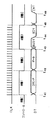
 従来、フラッシュメモリ等の記憶媒体を内蔵するメモリカードが接続されるデータ処理装置が知られている。この種のデータ処理装置と、このデータ処理装置に接続されるメモリカードについて図面を用いて説明する。 Conventionally, a data processing device to which a memory card having a built-in storage medium such as a flash memory is connected is known. A data processing device of this type and a memory card connected to the data processing device will be described with reference to the drawings.

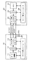
 データ処理装置100は、図11に示すように、データ処理部101と、レジスタ102と、ホスト側シリアルインターフェース回路103と、ホスト側コントローラ104とを備えている。また、メモリカード110は、メモリ111と、レジスタ112と、カード側シリアルインターフェース回路113と、カード側コントローラ114とを備えている。 As shown in FIG. 11, the data processing device 100 includes a data processing unit 101, a register 102, a host-side serial interface circuit 103, and a host-side controller 104. The memory card 110 includes a memory 111, a register 112, a card-side serial interface circuit 113, and a card-side controller 114.

 データ処理装置100のデータ処理部101は、メモリカード110に記憶したデータを読み出して各種データ処理を行い、各種データ処理をしてメモリカード110に書き込むデータを生成する。すなわち、データ処理部101は、メモリカード110を用いる各種装置のデータ処理回路となる。 The data processing unit 101 of the data processing device 100 reads data stored in the memory card 110, performs various data processing, performs various data processing, and generates data to be written to the memory card 110. That is, the data processing unit 101 is a data processing circuit of various devices using the memory card 110.

 レジスタ102は、データ処理部101とホスト側シリアルインターフェース103とのバッファである。すなわち、データ処理装置100は、データ処理部101からホスト側シリアルインターフェース回路103にデータを供給する場合は、このレジスタ102に一時データを格納した後にホスト側シリアルインターフェース回路103に供給する。同様に、データ処理装置100は、ホスト側シリアルインターフェース回路103からデータ処理部101にデータを供給する場合は、このレジスタ102に一時データを格納した後にデータ処理部101に供給する。 The register 102 is a buffer between the data processing unit 101 and the host-side serial interface 103. That is, when supplying data from the data processing unit 101 to the host-side serial interface circuit 103, the data processing apparatus 100 stores the temporary data in the register 102 and then supplies the data to the host-side serial interface circuit 103. Similarly, when data is supplied from the host-side serial interface circuit 103 to the data processing unit 101, the data processing device 100 stores the temporary data in the register 102 and then supplies the data to the data processing unit 101.

 ホスト側シリアルインターフェース回路103は、データ処理部101からレジスタ102を介して供給されるデータ及びカード側コントローラ114から供給されるコマンドをシリアル信号に変換してメモリカード110に供給する。また、ホスト側シリアルインターフェース回路103は、メモリカード110から供給されたシリアル信号のデータ及びコマンドをパラレル信号に変換して、データ処理部101及びカード側コントローラ114に供給する。 The host-side serial interface circuit 103 converts the data supplied from the data processing unit 101 via the register 102 and the command supplied from the card-side controller 114 into serial signals and supplies the serial signals to the memory card 110. The host-side serial interface circuit 103 converts the serial signal data and command supplied from the memory card 110 into a parallel signal, and supplies the parallel signal to the data processing unit 101 and the card-side controller 114.

 また、ホスト側シリアルインターフェース回路103は、データ及びコマンドの同期信号(CLK)及びチップセレクト信号(CS)をメモリカード110に供給する。さらに、ホスト側シリアルインターフェース回路103は、メモリカード110から供給されるビジー信号(BUSY)及びインタラプト信号(INTERRUPT)を取得する。 (4) The host-side serial interface circuit 103 supplies the data and command synchronization signal (CLK) and the chip select signal (CS) to the memory card 110. Further, the host-side serial interface circuit 103 acquires a busy signal (BUSY) and an interrupt signal (INTERRUPT) supplied from the memory card 110.

 ホスト側コントローラ104は、データ処理部101のデータ処理動作、ホスト側シリアルインターフェース回路103の各データの伝送動作の制御を行う。また、ホスト側コントローラ104は、メモリカード110への制御命令となるコマンドをレジスタ112を介してメモリカード110に供給する。 (4) The host-side controller 104 controls the data processing operation of the data processing unit 101 and the transmission operation of each data of the host-side serial interface circuit 103. Further, the host-side controller 104 supplies a command as a control command to the memory card 110 to the memory card 110 via the register 112.

 一方、メモリカード110のメモリ111は、例えば、フラッシュメモリ等からなりデータ処理部101から供給されたデータを記憶する。 On the other hand, the memory 111 of the memory card 110 is composed of, for example, a flash memory or the like and stores data supplied from the data processing unit 101.

 レジスタ112は、メモリ111とカード側シリアルインターフェース回路113とのバッファである。すなわち、メモリカード110は、メモリ111がデータ処理装置100からのデータを書き込む場合は、このレジスタ102に一時データを格納した後に書き込むデータをメモリ111に供給する。同様に、メモリカード110は、データ処理装置100がメモリ111からデータを読み出す場合は、このレジスタ102に一時データを格納した後に読み出すデータをカード側シリアルインターフェース回路113に供給する。このレジスタ112は、フラッシュメモリのページバッファの機能等を果たす回路である。 The register 112 is a buffer between the memory 111 and the card-side serial interface circuit 113. That is, when the memory 111 writes data from the data processing device 100, the memory card 110 supplies the data to be written to the memory 111 after storing the temporary data in the register 102. Similarly, when the data processing device 100 reads data from the memory 111, the memory card 110 supplies the data to be read after storing the temporary data in the register 102 to the card-side serial interface circuit 113. The register 112 is a circuit that performs a function of a page buffer of the flash memory and the like.

 カード側シリアルインターフェース回路113は、カード側コントローラ114の制御に基づき、メモリ111から供給されるパラレル信号のデータ及びカード側コントローラ114から供給されるコマンドをシリアル信号に変換してデータ処理装置100に供給する。また、カード側シリアルインターフェース回路113は、データ処理装置100から供給されるシリアル信号のデータ及びコマンドをパラレル信号に変換して、メモリ111及びカード側コントローラ114に供給する。 The card-side serial interface circuit 113 converts the parallel signal data supplied from the memory 111 and the command supplied from the card-side controller 114 into a serial signal based on the control of the card-side controller 114 and supplies the serial signal to the data processing device 100. I do. Further, the card-side serial interface circuit 113 converts the data and command of the serial signal supplied from the data processing device 100 into a parallel signal, and supplies the parallel signal to the memory 111 and the card-side controller 114.

 さらに、カード側シリアルインターフェース回路113は、データ及びコマンドの同期信号(CLK)及びチップセレクト信号(CS)をデータ処理装置100から取得する。さらにまた、カード側シリアルインターフェース回路113は、ビジー信号(BUSY)及びインタラプト信号(INTERRUPT)をデータ処理装置100に供給する。 (4) Further, the card-side serial interface circuit 113 acquires the data and command synchronization signal (CLK) and the chip select signal (CS) from the data processing device 100. Furthermore, the card side serial interface circuit 113 supplies a busy signal (BUSY) and an interrupt signal (INTERRUPT) to the data processing device 100.

 カード側コントローラ114は、メモリ111のデータの記憶動作、読み出し動作及び消去動作等をデータ処理装置100から供給されるコマンド等に基づき制御する。また、カード側コントローラ114は、カード側シリアルインターフェース回路113の各データの伝送動作の制御を行う。また、ホスト側コントローラ104は、メモリカード110のステータス信号となるビジー信号やインタラプト信号をメモリカード110から取得する。 The card-side controller 114 controls a data storage operation, a read operation, an erase operation, and the like of the memory 111 based on a command or the like supplied from the data processing device 100. Further, the card-side controller 114 controls the transmission operation of each data of the card-side serial interface circuit 113. In addition, the host-side controller 104 acquires a busy signal or an interrupt signal, which is a status signal of the memory card 110, from the memory card 110.

 以上のようなデータ処理装置100及びメモリカード110の間のデータの伝送は、ホスト側シリアルインターフェース回路103とカード側シリアルインターフェース回路113との間に設けられた伝送ラインを介して行われる。 Transmission of data between the data processing device 100 and the memory card 110 as described above is performed via a transmission line provided between the host-side serial interface circuit 103 and the card-side serial interface circuit 113.

 データ処理装置100のカード側シリアルインターフェース回路113と、メモリカード110のカード側シリアルインターフェース回路113の間には、CLKラインとCSラインとDTラインとBUSYラインとINTラインとの5本の信号ラインが設けられている。 Five signal lines of a CLK line, a CS line, a DT line, a BUSY line, and an INT line are provided between the card-side serial interface circuit 113 of the data processing device 100 and the card-side serial interface circuit 113 of the memory card 110. Is provided.

 DTラインには、主データであるデータ処理部101によりデータ処理をしてメモリ111に書き込むデータ及びメモリ111からデータ処理部101に読み出すデータが伝送される。また、DTラインには、データ処理装置100からメモリカード110に供給する制御命令となるコマンドと、メモリカード110からデータ処理装置100に供給されるコマンドが伝送される。すなわち、DTラインには、主データ及びコマンドがシリアル信号で双方向伝送される。 The data to be written to the memory 111 by the data processing unit 101 as main data and the data to be read from the memory 111 to the data processing unit 101 are transmitted to the DT line. Further, a command serving as a control command supplied from the data processing device 100 to the memory card 110 and a command supplied from the memory card 110 to the data processing device 100 are transmitted to the DT line. That is, main data and commands are bidirectionally transmitted as serial signals to the DT line.

 CLKラインには、上述したDTラインに伝送される主データ及びコマンドの同期信号がデータ処理装置100からメモリカード110に供給される。 The synchronization signal of the main data and the command transmitted to the DT line is supplied from the data processing device 100 to the memory card 110 on the #CLK line.

 CSラインには、いわゆるチップセレクト信号がデータ処理装置100からメモリカード110に供給される。このチップセレクト信号は、例えばハイとなっている期間、上述した主データ、コマンド及び同期信号が有効であることを示している。 A so-called chip select signal is supplied from the data processing device 100 to the memory card 110 on the CS line. This chip select signal indicates that the above-described main data, command, and synchronization signal are valid, for example, during a high period.

 BUSYラインには、メモリカード110が処理を行っていることを示すビジー信号が伝送される。例えば、メモリカード110が書き込み処理を行っている場合であって、データ処理装置100からのアクセスを禁止するときには、このビジー信号がメモリカード110からデータ処理装置100に供給される。 A busy signal indicating that the memory card 110 is performing a process is transmitted to the BUSY line. For example, when the memory card 110 is performing the writing process and the access from the data processing device 100 is prohibited, the busy signal is supplied from the memory card 110 to the data processing device 100.

 INTラインには、メモリカード110からデータ処理装置100に対しての割り込みを示すインタラプト信号がメモリカード110からデータ処理装置100に供給される。 An interrupt signal indicating an interrupt from the memory card 110 to the data processing device 100 is supplied from the memory card 110 to the data processing device 100 on the $ INT line.

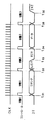
 このような伝送ラインに伝送される各種信号のタイムチャートは、図12に示すようになる。この図12に示すタイムチャートを用いて、メモリカード110に記憶するデータを読み出す場合について説明する。 タ イ ム A time chart of various signals transmitted to such a transmission line is as shown in FIG. A case where data stored in the memory card 110 is read will be described with reference to the time chart shown in FIG.

 まず、時刻t11において、データ処理装置100は、CSラインを介してチップセレクト信号をメモリカード110に供給する。データ処理装置100は、このチップセレクト信号とともに同期信号をCLKラインを介して供給する。メモリカード110は、このチップセレクト信号を取得することにより、データ処理装置100から供給されるコマンドを取得する準備をする。そして、データ処理装置100は、このチップセレクト信号を供給すると、DTラインを介して読み出し命令を示すコマンドとそのアドレスをメモリカード110に供給する。 At time t 11, the data processing apparatus 100 supplies the chip select signal to the memory card 110 through the CS line. The data processing device 100 supplies a synchronization signal along with the chip select signal via the CLK line. The memory card 110 prepares to acquire the command supplied from the data processing device 100 by acquiring the chip select signal. When the data processing device 100 supplies the chip select signal, the data processing device 100 supplies a command indicating a read command and its address to the memory card 110 via the DT line.

 データ処理装置100は、この読み出しコマンド等を供給し終えると、時刻t12において、このコマンドと同期信号の供給を停止する。メモリカード110は、コマンドの取得をし終えると、この供給されたコマンドに基づく制御を行うため、ビジー信号をデータ処理装置100に供給する。すなわち、メモリカード110は、指定されたアドレスの主データをメモリ111からレジスタ112に読み出す制御を行う。なお、このとき、データ処理装置100は、チップセレクト信号の供給は停止しない。 Data processing apparatus 100, after finishing supplying the read command or the like, at time t 12, to stop the supply of the command and synchronization signal. After completing the acquisition of the command, the memory card 110 supplies a busy signal to the data processing device 100 to perform control based on the supplied command. That is, the memory card 110 performs control to read main data at the specified address from the memory 111 to the register 112. At this time, the data processing device 100 does not stop supplying the chip select signal.

 メモリカード110は、レジスタ112に主データを読み出すと、時刻t13においてビジー信号の供給を停止する。すなわち、データ処理装置100に対して主データを伝送する準備ができたことを示すレディー状態を知らせる。 Memory card 110, reading the main data to the register 112 to stop the supply of the busy signal at time t 13. That is, it notifies the data processing apparatus 100 of a ready state indicating that the main data is ready to be transmitted.

 データ処理装置100は、ビジー信号の供給が停止したことを知ると、メモリカード110が供給したコマンドに基づく制御が終了したと判断して、時刻t14において同期信号をメモリカード110に供給する。そして、メモリカード110は、主データをDTラインを介してデータ処理装置100に伝送する。 Data processing device 100 knows that the supply of the busy signal is stopped, it is determined that the control based on the command memory card 110 is supplied has finished, and supplies the synchronization signal to the memory card 110 at time t 14. Then, the memory card 110 transmits the main data to the data processing device 100 via the DT line.

 そして、メモリカード110が主データの伝送を終了すると、データ処理装置100は、時刻t15において同期信号とチップセレクト信号の供給を停止する。 When the memory card 110 has completed the transmission of main data, the data processing apparatus 100 stops the supply of the synchronizing signal and the chip select signal at time t 15.

 なお、メモリカード110は、この読み出し処理をした結果等により、メモリカード110の内部状態に変化が生じた場合、時刻t16に示すように、INTラインを介して割り込みを示すインタラプト信号をデータ処理装置100に供給する。データ処理装置100は、このインタラプト信号が供給されると、この割り込み要因をメモリカード110から取得するため、チップセレクト信号とともに所定のコマンドをメモリカード110に供給する。 The memory card 110 by the reading process the result or the like, if a change in the internal state of the memory card 110 has occurred, as shown at time t 16, the data processing an interrupt signal indicating the interruption via the INT line Supply to the device 100. When the interrupt signal is supplied, the data processing device 100 supplies a predetermined command to the memory card 110 together with the chip select signal in order to acquire the interrupt factor from the memory card 110.

 以上のように、データ処理装置100は、主データ及びコマンドを伝送するDTライン及び同期信号を供給するCLKラインとともに、チップセレクト信号を供給するCSライン、ビジー信号を取得するBUSYライン及びインタラプト信号を取得するINTラインを設けてメモリカード110とのデータの伝送を実現している。 As described above, the data processing apparatus 100 transmits the CS line for supplying the chip select signal, the BUSY line for acquiring the busy signal, and the interrupt signal together with the DT line for transmitting the main data and the command and the CLK line for supplying the synchronization signal. By providing an INT line to be acquired, data transmission with the memory card 110 is realized.

 ところで、上述した外部記憶装置であるメモリカード110の小型化等を考えた場合、データ処理装置100とメモリカード110との信号ラインの数を少なくする必要が生じる。 By the way, when considering the miniaturization of the memory card 110 as the external storage device described above, it is necessary to reduce the number of signal lines between the data processing device 100 and the memory card 110.

特開昭60−51046号公報JP-A-60-51046

 本発明は、このような実情を鑑みてなされたものであり、主データをシリアル通信するためのデータ端子のほかに予備の端子であるリザーブ端子を設けることで、主データをシリアル通信を行うほか、リザーブ端子との組み合わせで更に他の機能を付加することができるデータ処理システム、データ処理装置、外部装置及びデータ伝送方法を提供することを目的とする。 The present invention has been made in view of such circumstances, and provides a reserve terminal which is a spare terminal in addition to a data terminal for serial communication of main data, thereby performing serial communication of main data. It is an object of the present invention to provide a data processing system, a data processing device, an external device, and a data transmission method to which other functions can be added in combination with a reserved terminal.

 本発明に係るデータ処理システムは、外部装置とデータの伝送を行なうデータ処理装置とを含むデータ処理システムにおいて、データ処理装置は、外部装置へのコマンドを生成し、外部装置からデータを受けるコントローラおよび上記外部装置と通信するための複数の端子を有し、外部装置は、略カードの形状、上記データ処理装置からのコマンドを受けるコントローラ、および上記データ処理装置と通信するための複数の端子を有し、上記外部装置の上記端子は、上記外部装置と上記データ処理装置が主データをシリアル通信するためのデータ端子と、予備の端子であるリザーブ端子とを有する。 A data processing system according to the present invention is a data processing system including an external device and a data processing device that transmits data, wherein the data processing device generates a command to the external device, receives a data from the external device, and The external device has a plurality of terminals for communicating with the external device. The external device has a substantially card shape, a controller for receiving a command from the data processing device, and a plurality of terminals for communicating with the data processing device. The terminal of the external device has a data terminal through which the external device and the data processing device serially communicate main data, and a reserve terminal that is a spare terminal.

 本発明に係るデータ処理装置は、外部装置とデータ伝送を行うデータ処理装置において、上記外部装置へのコマンドを生成し、上記外部装置からデータを受けるコントローラおよび上記外部装置と通信するための複数の端子を有し、上記複数の端子は、上記外部装置と主データをシリアル通信するためのデータ端子と、予備の端子であるリザーブ端子とを有する。 A data processing device according to the present invention is a data processing device that performs data transmission with an external device, generates a command to the external device, a controller that receives data from the external device, and a plurality of devices for communicating with the external device. A plurality of terminals including a data terminal for serially communicating main data with the external device and a reserve terminal serving as a spare terminal.

 本発明に係る外部装置は、データ処理装置とデータ伝送を行う外部装置において、略カードの形状、上記データ処理装置からのコマンドを受けるコントローラ、および上記データ処理装置と通信するための複数の端子を有し、上記端子は、上記外部装置と上記データ処理装置が主データをシリアル通信するためのデータ端子と、予備の端子であるリザーブ端子とを有する。 An external device according to the present invention is an external device that performs data transmission with a data processing device, and has a substantially card shape, a controller that receives a command from the data processing device, and a plurality of terminals for communicating with the data processing device. The terminal has a data terminal through which the external device and the data processing device serially communicate main data, and a reserve terminal that is a spare terminal.

 本発明に係るデータ伝送方法は、外部装置とデータ処理装置との間でデータ伝送を行うデータ伝送方法において、データ処理装置は、外部装置へのコマンドを生成し、外部装置からデータを受けるコントローラおよび上記外部装置と通信するための複数の端子を有し、外部装置は、略カードの形状、上記データ処理装置からのコマンドを受けるコントローラ、および上記データ処理装置と通信するための複数の端子を有し、上記外部装置の上記端子は、上記外部装置と上記データ処理装置が主データをシリアル通信するためのデータ端子と、予備の端子であるリザーブ端子とを有し、上記データ処理装置で生成されたコマンドに応じて上記外部装置と上記データ処理装置との間で主データのシリアル通信を行う。 A data transmission method according to the present invention is a data transmission method for performing data transmission between an external device and a data processing device, wherein the data processing device generates a command to the external device and receives data from the external device. The external device has a plurality of terminals for communicating with the external device. The external device has a substantially card shape, a controller for receiving a command from the data processing device, and a plurality of terminals for communicating with the data processing device. The terminal of the external device has a data terminal for serial communication of main data between the external device and the data processing device, and a reserve terminal that is a spare terminal, and is generated by the data processing device. In response to the command, serial communication of main data is performed between the external device and the data processing device.

 上述したように、本発明は、主データをシリアル通信するためのデータ端子と、予備の端子であるリザーブ端子を有することから、主データをシリアル通信を行うほか、リザーブ端子との組み合わせで更に他の機能を付加することができる。 As described above, the present invention has a data terminal for serial communication of main data and a reserve terminal that is a spare terminal. Function can be added.

 以下、本発明に係るデータ処理装置及びデータ伝送方法に用いられるデータ処理装置とこのデータ処理装置に用いられる外部記憶装置であるメモリカードについて、図面を参照しながら説明する。 Hereinafter, a data processing device used in the data processing device and the data transmission method according to the present invention and a memory card which is an external storage device used in the data processing device will be described with reference to the drawings.

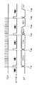
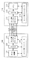
 まず、本発明にデータ処理システムを構成するデータ処理装置を説明すると、このデータ処理装置10は、図1に示すように、データ処理部11と、レジスタ12と、ホスト側シリアルインターフェース回路13と、ホスト側コントローラ14とを備えている。また、メモリカード20は、外観がカード状の記憶媒体であり、データ処理装置10に接続されて外部記憶装置として用いられる。メモリカード20は、メモリ21とレジスタ22とカード側シリアルインターフェース回路23とカード側コントローラ24とを備えている。 First, a data processing device constituting a data processing system according to the present invention will be described. As shown in FIG. 1, the data processing device 10 includes a data processing unit 11, a register 12, a host-side serial interface circuit 13, And a host-side controller 14. The memory card 20 is a storage medium having a card-like appearance, and is connected to the data processing device 10 and used as an external storage device. The memory card 20 includes a memory 21, a register 22, a card-side serial interface circuit 23, and a card-side controller 24.

 データ処理装置10のデータ処理部11は、メモリカード20に記憶したデータを読み出して各種データ処理を行い、各種データ処理をしてメモリカード20に書き込むデータを生成する。このデータ処理部11は、メモリカード20を用いる例えばコンピュータ装置や、デジタルオーディオ信号の記録再生装置、カメラ装置等のオーディオビジュアル機器のデータ処理回路となる。 The data processing unit 11 of the data processing device 10 reads data stored in the memory card 20, performs various data processing, and performs various data processing to generate data to be written to the memory card 20. The data processing unit 11 is a data processing circuit of an audiovisual device such as a computer device using the memory card 20, a recording / reproducing device for digital audio signals, and a camera device.

 レジスタ12は、データ処理部11とホスト側シリアルインターフェース13とのバッファである。すなわち、データ処理装置10は、データ処理部11からホスト側シリアルインターフェース回路13にデータを供給する場合は、データをこのレジスタ12に一時格納した後にホスト側シリアルインターフェース回路13に供給する。同様に、データ処理装置10は、ホスト側シリアルインターフェース回路13からデータ処理部11にデータを供給する場合は、データをこのレジスタ12に一時格納した後にデータ処理部11に供給する。 The register 12 is a buffer between the data processing unit 11 and the host-side serial interface 13. That is, when supplying data from the data processing unit 11 to the host-side serial interface circuit 13, the data processing device 10 temporarily stores the data in the register 12 and then supplies the data to the host-side serial interface circuit 13. Similarly, when data is supplied from the host-side serial interface circuit 13 to the data processing unit 11, the data processing device 10 temporarily stores the data in the register 12 and then supplies the data to the data processing unit 11.

 ホスト側シリアルインターフェース回路13は、データ処理部11からレジスタ12を介して供給されたデータ及びカード側コントローラ24から供給されるコマンドをシリアル信号に変換してメモリカード20に供給する。また、ホスト側シリアルインターフェース回路13は、メモリカード20から供給されたシリアル信号のデータ及びコマンドをパラレル信号に変換してデータ処理部11及びカード側コントローラ24に供給する。 The host-side serial interface circuit 13 converts the data supplied from the data processing unit 11 via the register 12 and the command supplied from the card-side controller 24 into serial signals and supplies the serial signals to the memory card 20. Further, the host-side serial interface circuit 13 converts the data and command of the serial signal supplied from the memory card 20 into a parallel signal and supplies the parallel signal to the data processing unit 11 and the card-side controller 24.

 また、ホスト側シリアルインターフェース回路13は、各種データ及びコマンドの同期信号(CLK)等をメモリカード20に供給する。さらに、ホスト側シリアルインターフェース回路13は、メモリカード20から供給されこのメモリカード20の動作状態を示すステータス(STATUS)信号を取得する。 (4) The host-side serial interface circuit 13 supplies a synchronization signal (CLK) of various data and commands to the memory card 20. Further, the host-side serial interface circuit 13 acquires a status (STATUS) signal supplied from the memory card 20 and indicating the operation state of the memory card 20.

 ホスト側コントローラ14は、データ処理部11のデータ処理動作、ホスト側シリアルインターフェース回路13の各データの伝送動作の制御を行う。また、ホスト側コントローラ14は、メモリカード20への制御命令となるコマンドをレジスタ22を介してメモリカード20に供給する。 (4) The host-side controller 14 controls the data processing operation of the data processing unit 11 and the transmission operation of each data of the host-side serial interface circuit 13. Further, the host-side controller 14 supplies a command that is a control command to the memory card 20 to the memory card 20 via the register 22.

 一方、メモリカード20のメモリ21は、例えば、フラッシュメモリ等からなり、データ処理部11から供給されたデータを記憶する。 On the other hand, the memory 21 of the memory card 20 is formed of, for example, a flash memory or the like, and stores the data supplied from the data processing unit 11.

 レジスタ22は、メモリ21とカード側シリアルインターフェース回路23とのバッファであり、メモリ21がデータ処理装置10からのデータを書き込む場合は、このレジスタ12に一時データを格納した後に書き込むデータをメモリ21に供給する。同様に、データ処理装置10がメモリ21からデータを読み出す場合は、このレジスタ12に一時データを格納した後に読み出すデータをカード側シリアルインターフェース回路23に供給する。すなわち、このレジスタ22は、フラッシュメモリのいわゆるページバッファの機能等を果たす回路である。 The register 22 is a buffer between the memory 21 and the card-side serial interface circuit 23. When the memory 21 writes data from the data processing device 10, the data to be written after storing the temporary data in the register 12 is stored in the memory 21. Supply. Similarly, when the data processing device 10 reads data from the memory 21, it stores the temporary data in the register 12 and supplies the read data to the card-side serial interface circuit 23. That is, the register 22 is a circuit that performs the function of a so-called page buffer of the flash memory and the like.

 カード側シリアルインターフェース回路23は、カード側コントローラ24の制御に基づきメモリ21から供給されるパラレル信号のデータ及びカード側コントローラ24から供給されるコマンドをシリアル信号に変換してデータ処理装置10に供給する。また、カード側シリアルインターフェース回路23は、データ処理装置10から供給されるシリアル信号のデータ及びコマンドをパラレル信号に変換してメモリ21及びカード側コントローラ24に供給する。 The card-side serial interface circuit 23 converts the parallel signal data supplied from the memory 21 and the command supplied from the card-side controller 24 into a serial signal based on the control of the card-side controller 24 and supplies the serial signal to the data processing device 10. . Further, the card-side serial interface circuit 23 converts the data and command of the serial signal supplied from the data processing device 10 into a parallel signal and supplies the parallel signal to the memory 21 and the card-side controller 24.

 また、カード側シリアルインターフェース回路23は、各種データ及びコマンドの同期信号(CLK)等をデータ処理装置10から取得する。さらに、カード側シリアルインターフェース回路23は、ステータス信号をデータ処理装置10に供給する。 {Circle around (4)} The card-side serial interface circuit 23 acquires various data and command synchronization signals (CLK) from the data processing device 10. Further, the card-side serial interface circuit 23 supplies a status signal to the data processing device 10.

 カード側コントローラ24は、メモリ21のデータの記憶動作、読み出し動作及び消去動作等をデータ処理装置10から供給されるコマンド等に基づき制御する。また、カード側コントローラ24は、カード側シリアルインターフェース回路23の各データの伝送動作の制御を行う。さらに、ホスト側コントローラ14は、メモリカード20へのステータス信号をメモリカード20に供給する制御を行う。 The card-side controller 24 controls the operation of storing, reading, and erasing data in the memory 21 based on commands and the like supplied from the data processing device 10. Further, the card-side controller 24 controls the transmission operation of each data of the card-side serial interface circuit 23. Further, the host-side controller 14 controls to supply a status signal to the memory card 20 to the memory card 20.

 以上のようなデータ処理装置10及びメモリカード20の間のデータの伝送は、ホスト側シリアルインターフェース回路13とカード側シリアルインターフェース回路23との間に設けられた伝送ラインを介して行われる。 Transmission of data between the data processing device 10 and the memory card 20 as described above is performed via a transmission line provided between the host-side serial interface circuit 13 and the card-side serial interface circuit 23.

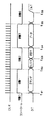
 データ処理装置10のカード側シリアルインターフェース回路23と、メモリカード20のカード側シリアルインターフェース回路23の間には、CLKライン31とコントロールライン32とDTライン33との3本の信号ラインが設けられている。 Between the card-side serial interface circuit 23 of the data processing device 10 and the card-side serial interface circuit 23 of the memory card 20, three signal lines of a CLK line 31, a control line 32, and a DT line 33 are provided. I have.

 DTライン33には、主データであるデータ処理部11によりデータ処理をしてメモリ21に書き込むデータ及びメモリ21からデータ処理部11に読み出すデータが伝送される。このDTライン33には、データ処理装置10からメモリカード20に供給する制御命令となるコマンドと、メモリカード20からデータ処理装置10に供給されるコマンドが伝送される。すなわち、DTライン33には、主データ及びコマンドがシリアル信号で双方向伝送される。 The data to be written to the memory 21 by the data processing unit 11 as main data and the data to be read from the memory 21 to the data processing unit 11 are transmitted to the DT line 33. To the DT line 33, a command serving as a control command supplied from the data processing device 10 to the memory card 20 and a command supplied from the memory card 20 to the data processing device 10 are transmitted. That is, main data and commands are bi-directionally transmitted to the DT line 33 as serial signals.

 さらに、DTライン33には、一端が接地された抵抗33aが取り付けられている。この抵抗33aは、いわゆるプルダウン抵抗であり、ホスト側シリアルインターフェース回路13とカード側シリアルインターフェース回路23との間でのDTライン33による信号の送受信がなされていないとき、DTライン33の信号レベルはローレベルとなる。換言すれば、DTライン33による信号の送受信がなされていないとき、DTライン33の信号レベルは抵抗33aの抵抗値等によって定まる一定のレベルとなる。 抵抗 Further, the DT line 33 is provided with a resistor 33a having one end grounded. The resistor 33a is a so-called pull-down resistor. When a signal is not transmitted and received by the DT line 33 between the host-side serial interface circuit 13 and the card-side serial interface circuit 23, the signal level of the DT line 33 is low. Level. In other words, when signals are not transmitted and received by the DT line 33, the signal level of the DT line 33 is a constant level determined by the resistance value of the resistor 33a and the like.

 なお、ここで、抵抗33aとしていわゆるプルダウン抵抗を採用し、DTライン33による信号の送受信がなされていないとき、DTライン33の信号レベルがローレベルとなるようにしたが、抵抗33aとしていわゆるプルアップ抵抗を採用し、DTライン33による信号の送受信がなされていないとき、DTライン33の信号レベルがハイレベルとなるようにしてもよい。 Here, a so-called pull-down resistor is employed as the resistor 33a, and the signal level of the DT line 33 is set to a low level when signals are not transmitted and received by the DT line 33. A resistor may be employed so that the signal level of the DT line 33 becomes a high level when signals are not transmitted and received by the DT line 33.

 CLKライン31には、上述したDTライン33に伝送される主データ及びコマンドの同期信号がデータ処理装置10からメモリカード20に伝送される。 The synchronization signal of the main data and the command transmitted to the DT line 33 is transmitted from the data processing device 10 to the memory card 20 on the CLK line 31.

 コントロールライン32には、コントロール信号がデータ処理装置10からメモリカード20に伝送される。このコントロール信号が供給されている期間、例えばハイとなっている期間上述した主データ及びコマンドが伝送される。 The control signal is transmitted from the data processing device 10 to the memory card 20 on the control line 32. While the control signal is being supplied, for example, during a high period, the above-described main data and command are transmitted.

 ここで、上述したDTライン33には、主データ及びコマンドに加えて、メモリカード20の動作状態を示すステータス(STATUS)信号がメモリカード20からデータ処理装置10に供給される。このメモリカード20からのステータス信号は、DTライン33に主データ及びコマンドが伝送されていない期間、すなわち、コントロール信号が供給されていない期間、例えばローの期間に供給される。このステータス信号には、メモリカード20が処理を行っていることを示すビジー(BUSY)信号がある。例えば、メモリカード20が書き込み処理を行っている場合であってデータ処理装置10からのアクセスを禁止するときには、ビジー信号がメモリカード20からデータ処理装置10に供給される。 Here, in addition to the main data and the command, a status (STATUS) signal indicating the operation state of the memory card 20 is supplied from the memory card 20 to the data processing device 10 to the DT line 33 described above. The status signal from the memory card 20 is supplied during a period when the main data and the command are not transmitted to the DT line 33, that is, during a period when the control signal is not supplied, for example, during a low period. The status signal includes a busy (BUSY) signal indicating that the memory card 20 is performing a process. For example, when access from the data processing device 10 is prohibited when the memory card 20 is performing a writing process, a busy signal is supplied from the memory card 20 to the data processing device 10.

 また、ステータス信号には、メモリカード20からデータ処理装置10に対しての割り込みを示すインタラプト(INTERRPUT)信号がある。例えば、メモリカード20からデータ処理装置10に対して割り込み命令を要求するときには、このインタラプト信号が供給される。なお、このビジー信号やインタラプト信号は一例であり、ステータス信号としてメモリカード20の動作状態を示す信号であればどのような信号であってもよい。 The status signal includes an interrupt (INTERRPUT) signal indicating an interrupt from the memory card 20 to the data processing device 10. For example, this interrupt signal is supplied when the memory card 20 requests an interrupt command to the data processing device 10. Note that the busy signal and the interrupt signal are merely examples, and any signal may be used as the status signal as long as the signal indicates the operation state of the memory card 20.

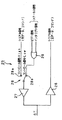
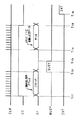
 このように、コントロール信号が供給されていない期間にステータス信号を供給するには、図2に示すような出力回路をメモリカード20に設ければよい。 In order to supply a status signal during a period in which a control signal is not supplied, an output circuit as shown in FIG.

 メモリカード20の出力回路25は、カード側シリアルインターフェース回路23とDTライン33の入出力端子との間に設けられ、入力バッファ26と出力バッファ27と切換スイッチ28とオア回路29とからなる。 The output circuit 25 of the memory card 20 is provided between the card-side serial interface circuit 23 and the input / output terminal of the DT line 33, and includes an input buffer 26, an output buffer 27, a changeover switch 28, and an OR circuit 29.

 入力バッファ26は、DTライン33と接続され、データ処理装置10から供給されたシリアル信号が入力されこのシリアル信号をカード側シリアルインターフェース回路23に供給する。 The input buffer 26 is connected to the DT line 33, receives a serial signal supplied from the data processing device 10, and supplies the serial signal to the card-side serial interface circuit 23.

 出力バッファ27は、切換スイッチ28を介して供給されるシリアル信号、ビジー信号及びインタラプト信号をDTライン33に出力する。 (4) The output buffer 27 outputs the serial signal, the busy signal, and the interrupt signal supplied through the changeover switch 28 to the DT line 33.

 また、カード側コントローラ24から供給されるビジー信号及びインタラプト信号は、オア回路23により論理和がとられ、切換スイッチ28の端子28bに供給される。また、カード側シリアルインターフェース回路23から供給されるシリアル信号は、切換スイッチ28の端子28aに供給される。 {Circle around (2)} The busy signal and the interrupt signal supplied from the card-side controller 24 are ORed by the OR circuit 23 and supplied to the terminal 28b of the changeover switch 28. Further, a serial signal supplied from the card-side serial interface circuit 23 is supplied to a terminal 28 a of the changeover switch 28.

 切換スイッチ28は、コントロール信号がハイのときは、端子28a側に切り換えられる。切換スイッチ28が端子28a側に切り換えられると、カード側シリアルインターフェース回路23からのシリアル信号が、出力バッファ27に供給される。また、切換スイッチ28は、コントロール信号がローのときは、端子28b側に切り換えられる。切換スイッチ28が端子28b側に切り換えられると、カード側コントローラ24からのビジー信号及びインタラプト信号等のステータス信号は出力バッファ27に供給される。 The switch 28 is switched to the terminal 28a when the control signal is high. When the changeover switch 28 is switched to the terminal 28a side, a serial signal from the card-side serial interface circuit 23 is supplied to the output buffer 27. The switch 28 is switched to the terminal 28b when the control signal is low. When the changeover switch 28 is switched to the terminal 28b side, a status signal such as a busy signal and an interrupt signal from the card-side controller 24 is supplied to the output buffer 27.

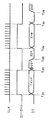
 このような伝送ラインに伝送される各種信号のタイムチャートは、図3に示すようになる。この図3に示すタイムチャートを用いて、メモリカード20に記憶する主データを読み出す場合について説明する。 タ イ ム A time chart of various signals transmitted to such a transmission line is as shown in FIG. The case where the main data stored in the memory card 20 is read using the time chart shown in FIG. 3 will be described.

 まず、時刻t21において、データ処理装置10は、コントロールライン32を介してコントロール信号をメモリカード20に供給する。メモリカード20は、このコントロール信号を取得することによりデータ処理装置10から供給されるコマンドを取得する準備をする。データ処理装置10は、このコントロール信号を供給するとともに、DTライン33を介して読み出し命令を示すコマンド等をメモリカード20に供給する。また、データ処理装置10は、このコマンド等とともにCLKライン31を介して同期信号をメモリカード20に供給する。 At time t 21, the data processing apparatus 10 supplies a control signal to the memory card 20 via the control line 32. The memory card 20 prepares to acquire the command supplied from the data processing device 10 by acquiring the control signal. The data processing device 10 supplies the control signal and a command indicating a read command to the memory card 20 via the DT line 33. Further, the data processing device 10 supplies a synchronization signal to the memory card 20 via the CLK line 31 together with the command and the like.

 データ処理装置10は、この読み出しコマンド等を供給し終えると、時刻t22において、コマンド、コントロール信号及び同期信号の供給を停止する。なお、同期信号は、この時刻t22において供給を停止しなくてもよい。 Data processor 10, after finishing supplying the read command or the like, at time t 22, stops the supply of the command, control and synchronization signals. Note that the synchronization signal does not have to stop the supply at time t 22.

 メモリカード20は、コマンドの取得をし終えると、この供給されたコマンドに基づく制御を行うため、ビジー信号をDTライン33を介してデータ処理装置10に供給する。データ処理装置10は、この時点でコントロール信号を供給していないため、メモリカード20から供給された信号がビジー信号であるということを判断することができる。メモリカード20は、ビジー信号を供給すると、指定されたアドレスの主データをメモリ21からレジスタ22に読み出す。 When the memory card 20 finishes acquiring the command, the memory card 20 supplies a busy signal to the data processing device 10 via the DT line 33 in order to perform control based on the supplied command. Since the data processing device 10 has not supplied the control signal at this time, it can determine that the signal supplied from the memory card 20 is a busy signal. When supplying the busy signal, the memory card 20 reads the main data at the specified address from the memory 21 to the register 22.

 メモリカード20は、レジスタ22に主データを読み出すと、時刻t23においてDTライン33を介してビジー信号の供給を停止する。すなわち、データ処理装置10に対して主データを供給する準備ができたことを示すレディー状態を知らせる。 Memory card 20 is reading the main data to the register 22 to stop the supply of the busy signal through the DT line 33 at time t 23. That is, a ready state indicating that the main data is ready to be supplied to the data processing apparatus 10 is notified.

 データ処理装置10は、時刻t24において、ビジー信号の供給が停止したことを知ると、メモリカード20が供給したコマンドに基づく制御が終了したと判断してコントロール信号と同期信号の供給をする。メモリカード20は、コントロール信号が供給されたことに基づき主データをDTライン33を介してこの供給された同期信号に同期させてデータ処理装置10に伝送する。 Data processor 10 at time t 24, knowing that the supply of the busy signal is stopped, the supply of the control signal and the synchronization signal to determine the control based on the command memory card 20 is supplied has finished. The memory card 20 transmits the main data to the data processing device 10 via the DT line 33 in synchronization with the supplied synchronization signal based on the supply of the control signal.

 メモリカード20が主データの伝送を終了すると、データ処理装置10は、時刻t25において同期信号とコントロール信号の供給を停止する。 When the memory card 20 has completed the transmission of main data, the data processing apparatus 10 stops the supply of the synchronizing signal and the control signal at time t 25.

 なお、メモリカード20は、この読み出し処理をした結果等により、メモリカード20の内部状態に変化が生じた場合は、必要に応じて時刻t26に示すようにDTライン33を介して割り込みを示すインタラプト信号をデータ処理装置10に供給する。データ処理装置10は、コントロール信号を供給していないことからメモリカード20から供給された信号がインタラプト信号であると判断でき、このインタラプト信号が供給されると、例えば、この割り込み要因をメモリカード20から取得するためコントロール信号を供給して対応したコマンドの供給を行う。 The memory card 20 by the read processing result and the like, if a change in the internal state of the memory card 20 has occurred, indicates an interrupt through the DT line 33 as shown at time t 26 as required An interrupt signal is supplied to the data processing device 10. Since the data processing device 10 does not supply the control signal, the data processing device 10 can determine that the signal supplied from the memory card 20 is an interrupt signal. , A control signal is supplied, and a corresponding command is supplied.

 以上のように、データ処理装置10及びメモリカード20では、メモリカード20からのステータス信号をDTライン33を用いて伝送することにより信号ラインを少なくすることができる。従って、ビジー信号やインタラプト信号のための信号ラインを特別に設ける必要がなく、簡単な構成で確実なデータの伝送をすることができる。また、インタラプト信号を設けずにデータ処理装置とメモリカードの間でデータの伝送を行った場合には、必ず一定時間毎ポーリングを行わなければならなかったが、このデータ処理装置10ではポーリングの必要がない。 As described above, in the data processing device 10 and the memory card 20, the number of signal lines can be reduced by transmitting the status signal from the memory card 20 using the DT line 33. Therefore, there is no need to provide a signal line for a busy signal or an interrupt signal, and reliable data transmission can be achieved with a simple configuration. Further, when data is transmitted between the data processing device and the memory card without providing an interrupt signal, polling must be performed at fixed time intervals. However, this data processing device 10 requires polling. There is no.

 ところで、以上のようなデータ処理装置10とメモリカード20との間のデータ伝送の場合、データ処理装置10からメモリカード20に供給するコマンドの内容、又はメモリカード20からデータ処理装置10に供給するコマンドの内容は予めホスト側コントローラ14やカード側コントローラ24により定められている。例えば、書き込みコマンド、読み出しコマンド又は消去コマンド等が予め定められている。これらのコマンドがDTライン33を介して伝送された場合、この後にDTライン33に伝送されるデータやコマンド、あるいは、ステータス信号の順序は必ず決定される。 By the way, in the case of data transmission between the data processing device 10 and the memory card 20 as described above, the content of a command supplied from the data processing device 10 to the memory card 20 or supplied from the memory card 20 to the data processing device 10. The contents of the command are determined in advance by the host-side controller 14 and the card-side controller 24. For example, a write command, a read command, an erase command, and the like are predetermined. When these commands are transmitted via the DT line 33, the order of data, commands, or status signals subsequently transmitted to the DT line 33 is always determined.

 具体的には、データ処理装置10からメモリカード20に対して書き込みコマンドが伝送された場合には、この書き込みコマンドの後にメモリカード20に書き込もうとする主データがデータ処理装置10からメモリカード20に伝送される。書き込みコマンド及び主データが伝送されたメモリカード20は、当該主データの書き込み処理を行っている間、ビジー信号をデータ処理装置10へ出力し、当該主データの書き込み処理が完了したらレディ信号をデータ処理装置10へ出力する。また、データ処理装置10からメモリカード20に対して読み出しコマンドが伝送された場合、メモリカード20は、当該読み出しコマンドに応じた主データの読み出し処理を行う。この読み出し処理を行っている間メモリカード20はビジー信号をデータ処理装置10へ出力し、読み出し処理が完了したらメモリカード20はレディ信号をデータ処理装置10へ出力する。データ処理装置10がレディ信号を受け取った後、メモリカード20からデータ処理装置10に対して主データが伝送され、これにより主データの読み出しが行われる。 Specifically, when a write command is transmitted from the data processing device 10 to the memory card 20, main data to be written to the memory card 20 after the write command is transmitted from the data processing device 10 to the memory card 20. Transmitted. The memory card 20 to which the write command and the main data have been transmitted outputs a busy signal to the data processing device 10 during the writing of the main data, and outputs a ready signal when the writing of the main data is completed. Output to the processing device 10. When a read command is transmitted from the data processing device 10 to the memory card 20, the memory card 20 performs a main data read process according to the read command. During this reading process, the memory card 20 outputs a busy signal to the data processing device 10, and when the reading process is completed, the memory card 20 outputs a ready signal to the data processing device 10. After the data processing device 10 receives the ready signal, the main data is transmitted from the memory card 20 to the data processing device 10, whereby the main data is read.

 そこで、以下に第2のデータ伝送方法として、このようにDTライン33によって伝送されるデータの内容やその順序等がコマンドにより予め定められている場合について説明する。 Therefore, a case will be described below as a second data transmission method in which the contents and the order of the data transmitted by the DT line 33 are predetermined by a command.

 この第2のデータ伝送方法では、コントロール信号を切り換えることによって、DTライン33を伝送するデータの状態を設定する。すなわち、コントロール信号を切り換えることによって、伝送するデータの状態を確定してデータの伝送を行う。 In the second data transmission method, the state of data transmitted on the DT line 33 is set by switching control signals. That is, by switching the control signal, the state of the data to be transmitted is determined and the data is transmitted.

 DTライン33によって伝送されるデータの状態は、以下のように設定される。まず、データ処理装置10からメモリカード20に対して何等制御命令すなわちコマンドを供給せず、また、メモリカード20が何等処理をしていない状態を初期状態として“状態0”とする。続いて、データ処理装置10からメモリカード20に対してコマンドを供給している状態、例えば、書き込みコマンド、読み出しコマンド又は消去コマンド等をDTライン33を介して供給している状態を“状態1”とする。その後、“状態1”で供給したコマンドに応じた処理が行われる“状態2”“状態3”へと推移し、“状態3”の後に“状態0”へと戻る。 The state of the data transmitted by the DT line 33 is set as follows. First, a state in which no control command, that is, a command is supplied from the data processing apparatus 10 to the memory card 20 and the memory card 20 is not performing any processing is set to “state 0” as an initial state. Subsequently, a state in which a command is supplied from the data processing device 10 to the memory card 20, for example, a state in which a write command, a read command, an erase command, or the like is supplied via the DT line 33 is “state 1”. And After that, the state changes to “state 2” and “state 3” in which processing according to the command supplied in “state 1” is performed, and returns to “state 0” after “state 3”.

 そして、コントロール信号は、このような“状態0”から“状態3”までの状態を切り換える。すなわち、“状態0”では、このコントロール信号はローとなっており、この“状態0”の状態からコントロール信号がハイとなると、“状態1”に切り換わる。続いて、“状態1”の状態からコントロール信号がローとなると“状態2”に切り換わる。続いて、“状態2”の状態からコントロール信号がハイとなると、“状態3”に切り換わる。最後に、“状態3”の状態からコントロール信号がローとなると、“状態0”に切り換わる。 (4) The control signal switches the state from “State 0” to “State 3”. That is, in the "state 0", the control signal is low, and when the control signal becomes high from the "state 0" state, the state is switched to the "state 1". Subsequently, when the control signal becomes low from the state of “state 1”, the state is switched to “state 2”. Subsequently, when the control signal becomes high from the state of “state 2”, the state is switched to “state 3”. Finally, when the control signal becomes low from the state of “state 3”, the state is switched to “state 0”.

 このように、コントロール信号を切り換えることで、DTライン33によって伝送されるデータの内容を切り換える。そして、データ処理装置10及びメモリカード20は、“状態1”において伝送されたコマンドの内容に応じて、次の“状態2”、“状態3”に伝送するデータの内容を確定しそれぞれの状態に応じた処理を行う。 内容 By switching the control signal, the content of the data transmitted by the DT line 33 is switched. Then, the data processing device 10 and the memory card 20 determine the content of the data to be transmitted in the next “state 2” and “state 3” according to the content of the command transmitted in “state 1”, and Is performed according to.

 具体的には、例えば、メモリカード20からの主データの読み出しを行う場合には、まず、“状態1”とされ、データ処理装置10からメモリカード20へ読み出しコマンドが伝送される。次に、“状態2”となり、読み出しコマンドに応じてメモリカード20によって主データの読み出し処理が行われる。この処理を行っている間、メモリカード20からデータ処理装置10にビジー信号が伝送され、当該処理が完了したら、メモリカード20からデータ処理装置10にレディ信号が伝送される。そして、データ処理装置10によってレディ信号が検出されたら“状態3”となり、メモリカード20から読み出された主データがDTライン33を介してメモリカード20からデータ処理装置10へ伝送される。そして、主データの伝送が完了したら“状態0”へ戻る。 {Specifically, for example, when reading main data from the memory card 20, the state is first set to “state 1”, and a read command is transmitted from the data processing device 10 to the memory card 20. Next, the state becomes “state 2”, and the main data is read by the memory card 20 in response to the read command. During this process, a busy signal is transmitted from the memory card 20 to the data processing device 10, and when the process is completed, a ready signal is transmitted from the memory card 20 to the data processing device 10. When the ready signal is detected by the data processing device 10, the state becomes “state 3”, and the main data read from the memory card 20 is transmitted from the memory card 20 to the data processing device 10 via the DT line 33. Then, when the transmission of the main data is completed, the state returns to “state 0”.

 あるいは、例えば、メモリカード20への主データの書き込みを行う場合には、まず、“状態1”とされ、データ処理装置10からメモリカード20へ書き込みコマンドが伝送される。次に、“状態2”となり、メモリカード20へ書き込む主データがDTライン33を介してデータ処理装置10からメモリカード20に伝送される。次に、“状態3”となり、書き込みコマンドに応じてメモリカード20によって主データの書き込み処理が行われる。この処理を行っている間、メモリカード20からデータ処理装置10へビジー信号が伝送され、当該処理が完了したら、メモリカード20からデータ処理装置10へレディ信号が伝送される。そして、データ処理装置10によってレディ信号が検出されたら“状態0”へ戻る。 Alternatively, for example, when writing the main data to the memory card 20, the state is first set to “state 1”, and a write command is transmitted from the data processing device 10 to the memory card 20. Next, the state becomes “state 2”, and the main data to be written to the memory card 20 is transmitted from the data processing device 10 to the memory card 20 via the DT line 33. Next, “State 3” is entered, and the main data is written by the memory card 20 in response to the write command. During this process, a busy signal is transmitted from the memory card 20 to the data processing device 10, and when the process is completed, a ready signal is transmitted from the memory card 20 to the data processing device 10. Then, when the ready signal is detected by the data processing device 10, the process returns to “state 0”.

 あるいは、例えば、メモリカード20に書き込まれている主データの消去を行う場合には、まず、“状態1”のときに、データ処理装置10からメモリカード20へ消去コマンドが伝送される。次に、“状態2”となり、消去コマンドに応じてメモリカード20によって主データの消去処理が行われる。この処理を行っている間、メモリカード20からデータ処理装置10にビジー信号が伝送され、当該処理が完了したら、メモリカード20からデータ処理装置10にレディ信号が伝送される。そして、データ処理装置10によってレディ信号が検出されたら“状態0”へ戻る。 {Alternatively, for example, when erasing the main data written in the memory card 20, first, in the “state 1”, the erasure command is transmitted from the data processing device 10 to the memory card 20. Next, the state becomes “state 2”, and the main data is erased by the memory card 20 in response to the erase command. During this process, a busy signal is transmitted from the memory card 20 to the data processing device 10, and when the process is completed, a ready signal is transmitted from the memory card 20 to the data processing device 10. Then, when the ready signal is detected by the data processing device 10, the process returns to “state 0”.

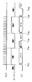
 このように、DTライン33に伝送されるデータに応じてコントロール信号を切り換えることにより、データ伝送の状態を制御する第2のデータ伝送方法について、図4及び図5のタイムチャートを参照して更に詳細に説明する。ここで、図4に示すタイムチャートは、データ処理装置10によってメモリカード20に書き込まれている主データを読み出すときのタイムチャートの一例である。また、図5に示すタイムチャートは、データ処理装置10によってメモリカード20に主データを書き込むときのタイムチャートの一例である。 As described above, the second data transmission method for controlling the data transmission state by switching the control signal according to the data transmitted to the DT line 33 will be further described with reference to the time charts of FIGS. This will be described in detail. Here, the time chart shown in FIG. 4 is an example of a time chart when the main data written in the memory card 20 is read by the data processing device 10. The time chart shown in FIG. 5 is an example of a time chart when main data is written to the memory card 20 by the data processing device 10.

 まず、図4を参照して主データの読み出しについて説明する。 First, reading of main data will be described with reference to FIG.

 データ処理装置10とメモリカード20との間で何等データの伝送が行われていない状態では、コントロール信号がローとなっており、“状態0”の初期状態となっている。そして、主データの読み出しに関する処理は、この“状態0”の初期状態から開始される。 (4) In a state where no data is transmitted between the data processing device 10 and the memory card 20, the control signal is low, which is an initial state of “state 0”. Then, the processing relating to the reading of the main data is started from the initial state of this “state 0”.

 主データの読み出しに関する処理を開始する時刻t31において、データ処理装置10は、コントロールライン32を介してメモリカード20に供給されるコントロール信号をローからハイに切り換える。従って、DTライン33に伝送されるデータの状態は、“状態0”から“状態1”に切り換えられる。メモリカード20は、このコントロール信号を取得することにより、“状態0”から“状態1”となったことを判断して、データ処理装置10から供給されるコマンドを取得する準備をする。そして、データ処理装置10は、この“状態1”のときに、DTライン33を介して読み出しコマンドをメモリカード20に供給するとともに、その同期信号をCLKライン31を介してメモリカード20に供給する。ここで、メモリカード20は、この“状態1”の状態で読み出しコマンドを取得することにより、後の“状態2”及び“状態3”でDTライン33を介して伝送されるデータの内容を確定する。 At time t 31 to start the processing relating to readout of the main data, the data processing apparatus 10 switches from the low control signal supplied to the memory card 20 to the high through the control line 32. Therefore, the state of the data transmitted to the DT line 33 is switched from “state 0” to “state 1”. By acquiring this control signal, the memory card 20 determines that the state has changed from “state 0” to “state 1”, and prepares to acquire the command supplied from the data processing device 10. Then, in the “state 1”, the data processing device 10 supplies a read command to the memory card 20 via the DT line 33 and supplies a synchronization signal to the memory card 20 via the CLK line 31. . Here, the memory card 20 acquires the read command in the state of “state 1”, thereby determining the content of the data transmitted via the DT line 33 in the subsequent “state 2” and “state 3”. I do.

 データ処理装置10は、読み出しコマンドの供給が完了した時刻t32においてコントロール信号をハイからローに切り換える。すなわち、“状態1”から“状態2”に切り換える。 The data processing apparatus 10 switches the control signal from the high at time t 32 to the supply of the read command has been completed low. That is, the state is switched from “state 1” to “state 2”.

 “状態2”となったら、メモリカード20は、“状態1”のときに供給された読み出しコマンドに基づく処理、具体的には、読み出しコマンドで指定されたアドレスの主データをメモリ21からレジスタ22に読み出す処理を行う。この処理を行っている間、メモリカード20は、ステータス信号としてビジー信号をDTライン33を介してデータ処理装置10に供給する。すなわち、“状態2”のとき、メモリカード20は、まず、ステータス信号としてビジー信号を出力する。このとき、データ処理装置10は、メモリカード20に供給したコマンドが読み出しコマンドであり、且つ現在の状態が“状態2”であることから、メモリカード20から出力されている信号がステータス信号であると判断する。 When the state becomes “state 2”, the memory card 20 performs processing based on the read command supplied in the state “state 1”, specifically, the main data at the address specified by the read command from the memory 21 to the register 22. To read the data. During this process, the memory card 20 supplies a busy signal as a status signal to the data processing device 10 via the DT line 33. That is, in the “state 2”, the memory card 20 first outputs a busy signal as a status signal. At this time, since the command supplied to the memory card 20 is a read command and the current state is “state 2”, the signal output from the memory card 20 is a status signal. Judge.

 その後、レジスタ22への主データの読み出しが完了したら、メモリカード20は、レジスタ22への主データの読み出しが完了した時刻t33において、DTライン33を介してステータス信号としてビジー信号の出力を停止してデータ処理装置10に対して主データを供給する準備ができたことを示すレディー信号の出力を開始する。すなわち、“状態2”のとき、メモリカード20は、レジスタ22への主データの読み出しが完了したらステータス信号としてレディ信号を出力する。 Thereafter, when the main data read is completed to the register 22, the memory card 20, at time t 33 to the main data reading has been completed to the register 22, stops outputting the busy signal as the status signal through the DT line 33 Then, the output of the ready signal indicating that the main data is ready to be supplied to the data processing device 10 is started. That is, in the “state 2”, the memory card 20 outputs a ready signal as a status signal when reading of the main data from the register 22 is completed.

 なお、本例では、“状態2”のときに、DTライン33を介してメモリカード20から出力される信号がハイのときをビジー信号として、ローのときをレディ信号としている。この“状態2”のとき、データ処理装置10は、メモリカード20に供給したコマンドが読み出しコマンドであり、且つ現在の状態が“状態2”であることから、メモリカード20から出力されている信号がステータス信号であると判断することができる。したがって、メモリカード20からDTライン33を介して出力される信号をハイからローに切り換えるだけでも、データ処理装置10は、当該信号がビジー信号からレディ信号に切り換わったことを検出することができる。 In this example, in the “state 2”, when the signal output from the memory card 20 via the DT line 33 is high, the signal is high, and when low, the signal is ready. In this “state 2”, the data processing device 10 outputs the signal output from the memory card 20 because the command supplied to the memory card 20 is a read command and the current state is “state 2”. Is a status signal. Therefore, the data processing device 10 can detect that the signal is switched from the busy signal to the ready signal only by switching the signal output from the memory card 20 via the DT line 33 from high to low. .

 データ処理装置10は、メモリカード20からレディ信号を受け取ったら、読み出しコマンドに基づくメモリカード20の処理が完了したと判断する。そして、読み出しコマンドに基づくメモリカード20の処理が完了したと判断された時刻t34においてコントロール信号をローからハイに切り換える。すなわち、“状態2”から“状態3”に切り換える。 When receiving the ready signal from the memory card 20, the data processing device 10 determines that the processing of the memory card 20 based on the read command has been completed. Then, switch the control signal from the low at time t 34 the processing of the memory card 20 is determined to be completed based on the read command high. That is, the state is switched from “state 2” to “state 3”.

 そして、“状態3”となったら、メモリカード20は、“状態2”のときにレジスタ22へ読み出した主データをDTライン33を介してデータ処理装置10に伝送する。その後、メモリカード20からデータ処理装置10への主データの伝送が完了した時刻t35において、データ処理装置10は、同期信号の供給を止めるとともにコントロール信号をハイからローに切り換える。すなわち、主データの伝送を行う“状態3”から、初期状態の“状態0”へと状態が戻される。 When the state becomes “state 3”, the memory card 20 transmits the main data read out to the register 22 at the time of “state 2” to the data processing device 10 via the DT line 33. Then, at time t 35 the transmission of main data has been completed from the memory card 20 to the data processing apparatus 10, the data processing apparatus 10 switches to the low control signal from high with stopping the supply of the synchronizing signal. That is, the state is returned from "state 3" in which the main data is transmitted to "state 0" of the initial state.

 なお、以上のような読み出し処理の影響等により、メモリカード20の内部状態に変化が生じて何らかの割り込み処理を行う必要が生じた場合、メモリカード20は、時刻t36に示すように、“状態0”のときに割り込みを示すインタラプト信号をDTライン33を介してデータ処理装置10に供給する。ここで、データ処理装置10は、“状態0”のときにメモリカード20からDTライン33を介して信号が供給されたときには当該信号がインタラプト信号であると判別するように予め設定しておく。これにより、この信号は、データ処理装置10によってインタラプト信号であると判断される。このインタラプト信号を受け取ったデータ処理装置10は、当該インタラプト信号に基づいて必要な処理を行う。 Incidentally, the influence of the reading process described above, if a change in the internal state of the memory card 20 is necessary to perform some interrupt processing occurs occurred, the memory card 20, as shown at time t 36, "state When the value is "0", an interrupt signal indicating an interrupt is supplied to the data processing device 10 via the DT line 33. Here, the data processing apparatus 10 is preset so that when a signal is supplied from the memory card 20 via the DT line 33 in the “state 0”, the signal is determined to be an interrupt signal. As a result, this signal is determined by the data processing device 10 to be an interrupt signal. The data processing device 10 receiving this interrupt signal performs necessary processing based on the interrupt signal.

 次に、図5を参照して主データの書き込みについて説明する。 Next, writing of main data will be described with reference to FIG.

 データ処理装置10とメモリカード20との間で何等データの伝送が行われていない状態では、コントロール信号がローとなっており、“状態0”の初期状態となっている。主データの書き込みに関する処理は、この“状態0”の初期状態から開始される。 (4) In a state where no data is transmitted between the data processing device 10 and the memory card 20, the control signal is low, which is an initial state of “state 0”. The process related to the writing of the main data is started from the initial state of “state 0”.

 主データの書き込みに関する処理を開始する時刻t41において、データ処理装置10は、コントロールライン32を介してメモリカード20に供給されるコントロール信号をローからハイに切り換える。従って、DTライン33に伝送されるデータの状態は、“状態0”から“状態1”に切り換えられる。メモリカード20は、このコントロール信号を取得することにより、“状態0”から“状態1”となったことを判断して、データ処理装置10から供給されるコマンドを取得する準備をする。そして、データ処理装置10は、この“状態1”のときに、DTライン33を介して書き込みコマンドをメモリカード20に供給するとともに、その同期信号をCLKライン31を介してメモリカード20に供給する。ここで、メモリカード20は、この“状態1”の状態で書き込みコマンドを取得することにより、後の“状態2”及び“状態3”でDTライン33を介して伝送されるデータの内容を確定する。 At time t 41 to start the processing relating to writing of the main data, the data processing apparatus 10 switches from the low control signal supplied to the memory card 20 to the high through the control line 32. Therefore, the state of the data transmitted to the DT line 33 is switched from “state 0” to “state 1”. By acquiring this control signal, the memory card 20 determines that the state has changed from “state 0” to “state 1”, and prepares to acquire the command supplied from the data processing device 10. Then, in the “state 1”, the data processing device 10 supplies the write command to the memory card 20 via the DT line 33 and supplies the synchronization signal to the memory card 20 via the CLK line 31. . Here, the memory card 20 acquires the write command in the “state 1” state, thereby determining the contents of the data transmitted via the DT line 33 in the subsequent “state 2” and “state 3”. I do.

 データ処理装置10は、書き込みコマンドの供給が完了した時刻t42において、コントロール信号をハイからローに切り換える。すなわち、“状態1”から“状態2”に切り換える。 Data processor 10 at time t 42 the supply of the write command has been completed, switches the control signal from high to low. That is, the state is switched from “state 1” to “state 2”.

 “状態2”のとき、データ処理装置10は、メモリカード20に書き込もうとする主データをDTライン33を介してメモリカード20へ伝送し、この主データのメモリカード20への伝送が完了した時刻t43においてコントロール信号をローからハイに切り換える。すなわち、“状態2”から“状態3”に切り換える。 In the “state 2”, the data processing device 10 transmits the main data to be written to the memory card 20 to the memory card 20 via the DT line 33, and the time when the transmission of the main data to the memory card 20 is completed. switch the control signal from low to high at t 43. That is, the state is switched from “state 2” to “state 3”.

 “状態3”となったら、メモリカード20は、“状態1”のときに供給された書き込みコマンドに基づく処理、具体的には、“状態2”のときにデータ処理装置10から伝送された主データをメモリ21に書き込む処理を行う。この処理を行っている間、メモリカード20は、ステータス信号としてビジー信号をDTライン33を介してデータ処理装置10に供給する。すなわち、“状態3”のとき、メモリカード20は、まず、ステータス信号としてビジー信号を出力する。このとき、データ処理装置10は、メモリカード20に供給したコマンドが書き込みコマンドであり、且つ現在の状態が“状態3”であることから、メモリカード20から出力されている信号がステータス信号であると判断する。 When the state becomes “state 3”, the memory card 20 performs processing based on the write command supplied in the state “state 1”, specifically, the main command transmitted from the data processing device 10 in the state “state 2”. A process of writing data to the memory 21 is performed. During this process, the memory card 20 supplies a busy signal as a status signal to the data processing device 10 via the DT line 33. That is, in the “state 3”, the memory card 20 first outputs a busy signal as a status signal. At this time, since the command supplied to the memory card 20 is a write command and the current state is “state 3”, the signal output from the memory card 20 is a status signal. Judge.

 その後、レジスタ22への主データの書き込みが完了したら、メモリカード20は、レジスタ22への主データの書き込みが完了した時刻t44において、ステータス信号として、ビジー信号の出力を停止して、主データの書き込みが完了したことを示すレディー信号の出力を開始する。すなわち、“状態3”のとき、メモリカード20は、レジスタ22への主データの書き込みが完了したらステータス信号としてレディ信号を出力する。 Thereafter, when the writing of the main data has been completed to the register 22, the memory card 20, at time t 44 a write of the main data has been completed to the register 22, as a status signal, it stops outputting the busy signal, the main data The output of a ready signal indicating that the writing of data has been completed is started. That is, in the “state 3”, the memory card 20 outputs a ready signal as a status signal when the writing of the main data to the register 22 is completed.

 なお、本例では、“状態3”のときに、DTライン33を介してメモリカード20から出力される信号がハイのときをビジー信号として、ローのときをレディ信号としている。この“状態3”のとき、データ処理装置10は、メモリカード20に供給したコマンドが書き込みコマンドであり、且つ現在の状態が“状態3”であることからメモリカード20から出力されている信号がステータス信号であると判断することができる。したがって、メモリカード20からDTライン33を介して出力される信号をハイからローに切り換えるだけでも、データ処理装置10は、当該信号がビジー信号からレディ信号に切り換わったことを検出することができる。 In this example, in the “state 3”, when the signal output from the memory card 20 via the DT line 33 is high, the signal is high, and when low, the signal is ready. In the “state 3”, the data processing device 10 outputs a signal output from the memory card 20 because the command supplied to the memory card 20 is a write command and the current state is the “state 3”. It can be determined that this is a status signal. Therefore, the data processing device 10 can detect that the signal is switched from the busy signal to the ready signal only by switching the signal output from the memory card 20 via the DT line 33 from high to low. .

 データ処理装置10は、メモリカード20からレディ信号を受け取ったら書き込みコマンドに基づくメモリカード20の処理が完了したと判断する。そして、書き込みコマンドに基づくメモリカード20の処理が完了したと判断された時刻t45において、データ処理装置10は、同期信号の供給を止めるとともに、コントロール信号をハイからローに切り換える。すなわち、主データの書き込みを行っている状態である“状態3”から、初期状態の“状態0”へと状態が戻される。 When receiving the ready signal from the memory card 20, the data processing device 10 determines that the processing of the memory card 20 based on the write command has been completed. Then, in the memory a time t 45 it is determined that the processing of the card 20 has been completed based on the write command, the data processing apparatus 10, as well as stopping the supply of the synchronizing signal, switches the control signal from high to low. That is, the state is returned from "state 3" in which the main data is being written to "state 0" in the initial state.

 なお、以上のような書き込み処理の影響等により、メモリカード20の内部状態に変化が生じて、何らかの割り込み処理を行う必要が生じた場合、メモリカード20は、時刻t46に示すように、“状態0”のときに割り込みを示すインタラプト信号をDTライン33を介してデータ処理装置10に供給する。ここで、データ処理装置10は、“状態0”のときにメモリカード20からDTライン33を介して信号が供給されたときには、当該信号がインタラプト信号であると判別するように予め設定しておく。これにより、この信号は、データ処理装置10によってインタラプト信号であると判断される。そして、このインタラプト信号を受け取ったデータ処理装置10は、当該インタラプト信号に基づいて必要な処理を行う。 Incidentally, the influence of above-mentioned writing process, the change in the internal state of the memory card 20 is generated, if the need to perform any interrupt processing occurs, the memory card 20, as shown at time t 46, " When the state is "0", an interrupt signal indicating an interrupt is supplied to the data processing device 10 via the DT line 33. Here, when a signal is supplied from the memory card 20 via the DT line 33 in the “state 0”, the data processing device 10 is preset to determine that the signal is an interrupt signal. . As a result, this signal is determined by the data processing device 10 to be an interrupt signal. Then, the data processing device 10 having received the interrupt signal performs necessary processing based on the interrupt signal.

 以上のように、本発明を適用したデータ処理装置10及びメモリカード20では、コントロール信号を切り換えてDTライン33に伝送するデータの内容を確定するようにしており、これにより、DTライン33によってコマンドや主データだけでなくステータス信号やインタラプト信号も伝送することが可能となっている。そのため、データ処理装置10とメモリカード20との間の信号ラインを少なくすることができる。従って、ビジー信号やインタラプト信号のための信号ラインを特別に設ける必要がなく、簡単な構成で確実なデータの伝送をすることができる。また、DTライン33に伝送させるデータの切り換えのオーバーヘッドを少なくすることもでき、データの伝送の効率が高くなる。 As described above, in the data processing device 10 and the memory card 20 to which the present invention is applied, the control signal is switched to determine the content of the data to be transmitted to the DT line 33. And not only main data but also status signals and interrupt signals can be transmitted. Therefore, the number of signal lines between the data processing device 10 and the memory card 20 can be reduced. Therefore, there is no need to provide a signal line for a busy signal or an interrupt signal, and reliable data transmission can be achieved with a simple configuration. In addition, the overhead of switching data to be transmitted to the DT line 33 can be reduced, and the efficiency of data transmission increases.

 なお、上述の例ではデータ処理装置10とメモリカード20の場合を挙げて説明したが、本発明をメモリカード20ではなく、他のデータ処理装置に適用することができる。この場合は、予め、伝送されるコマンド等を他のデータ処理装置に設定しておくことが必要となるが、メモリカード20に対するコマンドのみならず、あらゆるコマンドを伝送することができる。 In the above example, the case of using the data processing device 10 and the memory card 20 has been described. However, the present invention can be applied to other data processing devices instead of the memory card 20. In this case, it is necessary to set a command or the like to be transmitted in another data processing device in advance, but not only a command to the memory card 20 but also any command can be transmitted.

 また、データ処理装置10とメモリカード20との間の第2のデータの伝送方法の説明では、コントロール信号で切り換えるDTライン33の伝送データの内容を、状態0、状態1、状態2、状態3の4パターンについて例示して説明したが、この4パターンに限らず伝送するコマンドの内容に応じてこれ以上のパターンに切り換えてもよい。 Further, in the description of the second data transmission method between the data processing device 10 and the memory card 20, the contents of the transmission data of the DT line 33 switched by the control signal are described as state 0, state 1, state 2, state 3 Although the above four patterns have been exemplified and described, the present invention is not limited to these four patterns, and may be switched to more patterns according to the content of a command to be transmitted.

 さらに、データ処理装置10とメモリカード20との間の第2のデータの伝送方法の説明では、DTライン33の伝送データの状態をコントロール信号のオンオフで切り換える場合について説明したが、図6や図7に示すように、パルス信号で切り換えるようにしてもよい。なお、図6及び図7は、コントロール信号としてパルス信号を用いたときのタイムチャートであり、図6は、図4と同様にデータ処理装置10によってメモリカード20に書き込まれている主データを読み出すときのタイムチャート、図7は、図5と同様にデータ処理装置10によってメモリカード20に主データを書き込むときのタイムチャートである。 Further, in the description of the second data transmission method between the data processing device 10 and the memory card 20, the case where the state of the transmission data of the DT line 33 is switched by turning on / off the control signal has been described. As shown in FIG. 7, switching may be performed by a pulse signal. 6 and 7 are time charts when a pulse signal is used as a control signal. FIG. 6 reads out main data written in the memory card 20 by the data processing device 10 as in FIG. FIG. 7 is a time chart when the main data is written to the memory card 20 by the data processing device 10 as in FIG.

 さらに、以上説明したメモリカード20には、例えば、CLKライン31、コントロールライン32及びDTライン33の他に、1本の電源ライン、3本のグランドライン及び3本のリザーブラインを設けて合計10本の信号ラインを有している。なお、3本のリザーブラインを設けたときには、これら3本のリザーブラインをDTラインとして使用して先のDTライン33と合わせてDTラインを4本とし、これら4本のDTラインをパラレルに使用するようにしてもよい。また、3本のリザーブラインを設けたときには、これら3本のリザーブラインをそれぞれCLKライン、コントロールライン及びDTラインとして使用して、先のCLKライン31、コントロールライン32及びDTライン33と合わせて、CLKライン、コントロールライン及びDTラインの組みを2つ設けるようにしてもよい。 Further, the memory card 20 described above has, for example, one power line, three ground lines, and three reserved lines in addition to the CLK line 31, the control line 32, and the DT line 33, for a total of 10 lines. It has three signal lines. When three reserved lines are provided, these three reserved lines are used as DT lines to make four DT lines together with the DT line 33, and these four DT lines are used in parallel. You may make it. When three reserved lines are provided, these three reserved lines are used as a CLK line, a control line and a DT line, respectively, and are combined with the previous CLK line 31, control line 32 and DT line 33, Two sets of the CLK line, the control line, and the DT line may be provided.

 ところで、以上の説明で挙げた第2のデータ伝送方法において、DTライン33で伝送されるコマンドや主データについては、エラー訂正コード等を一緒に伝送することで、外部からのノイズ等に対処できるが、コントロールライン31で伝送されるコントロール信号については、ハイからローへの切り換え、又はローからハイへの切り換えだけで、“状態0”、“状態1”、“状態2”、“状態3”の推移を示すようにしているので外部からのノイズ等の影響を受けるおそれがある。 By the way, in the second data transmission method described above, the command and main data transmitted on the DT line 33 can cope with external noise and the like by transmitting an error correction code and the like together. However, with respect to the control signal transmitted on the control line 31, only the switching from high to low or from low to high causes “state 0”, “state 1”, “state 2”, “state 3”. , It may be affected by external noise or the like.

 例えば、図4及び図5に挙げた例では、“状態0”及び“状態2”のときにコントロール信号をローとして、“状態1”及び“状態3”のときにコントロール信号をハイとしている。そして、“状態0”と“状態2”との判別や、“状態1”と“状態3”との判別は、それらの状態の推移を追うことにより判別するようにしている。したがって、状態の推移が正しく検出されないと、メモリカード20は、“状態0”と“状態2”とを間違えて判断してしまったり、“状態1”と“状態3”とを間違えて判断してしまったりするおそれがある。 For example, in the examples shown in FIG. 4 and FIG. 5, the control signal is set to low in “state 0” and “state 2”, and set to high in “state 1” and “state 3”. The determination between “state 0” and “state 2” and the determination between “state 1” and “state 3” are made by following the transition of these states. Therefore, if the transition of the state is not correctly detected, the memory card 20 mistakenly determines “state 0” and “state 2” or misunderstands “state 1” and “state 3”. May be lost.

 例えば、図4に示すように主データの読み出しを行う際に、コントロール信号にノイズがのり、メモリカード20が“状態1”と“状態3”とを間違えて判断してしまうと、データ処理装置10からメモリカード20に送られるコマンドとメモリカード20から読み出された主データとがDTライン33上でぶつかってしまう可能性がある。 For example, when the main signal is read as shown in FIG. 4, if the control signal contains noise and the memory card 20 mistakenly determines “state 1” and “state 3”, the data processing device There is a possibility that the command sent from the memory card 10 to the memory card 20 and the main data read from the memory card 20 will collide on the DT line 33.

 また、図4に示すように主データの読み出しを行う際に、コントロール信号にノイズがのり、メモリカード20が“状態0”と“状態2”とを間違えて判断してしまうと、“状態2”のときに出力すべきビジー信号やレディ信号が“状態0”のときに送出されてしまったり、“状態0”のときに出力すべきインタラプト信号が“状態2”のときに送出されてしまったりする可能性がある。 Also, as shown in FIG. 4, when the main data is read, if noise is included in the control signal and the memory card 20 mistakenly determines “state 0” and “state 2”, “state 2” ”, The busy signal or ready signal to be output is“ State 0 ”, or the interrupt signal to be output when“ State 0 ”is“ State 2 ”. There is a possibility of rolling.

 さらに、図5に示すように主データの書き込みを行う際に、コントロール信号にノイズがのり、メモリカード20が“状態1”と“状態3”とを間違えて判断してしまうと、データ処理装置10からメモリカード20に送られるコマンドとメモリカード20から出力されるステータス信号とがDTライン33上でぶつかってしまう可能性がある。あるいは、データ処理装置10の側はメモリカード20からのレディ信号を待ち、メモリカード20の側はデータ処理装置10からのコマンドを待つような状態となり、DTライン33でのデータの送受信が止まってしまう可能性もある。 Further, as shown in FIG. 5, when the main data is written, noise is added to the control signal, and the memory card 20 mistakenly determines “state 1” and “state 3”. There is a possibility that a command sent from the memory card 10 to the memory card 20 and a status signal output from the memory card 20 will collide on the DT line 33. Alternatively, the data processing apparatus 10 waits for a ready signal from the memory card 20, the memory card 20 waits for a command from the data processing apparatus 10, and the data transmission / reception on the DT line 33 stops. There is also a possibility.

 さらにまた、図5に示すように主データの書き込みを行う際に、コントロール信号にノイズがのり、メモリカード20が“状態0”と“状態2”とを間違えて判断してしまうと、データ処理装置10からメモリカード20に送られる主データとメモリカード20から出力されたインタラプト信号がDTライン33上でぶつかってしまう可能性がある。 Furthermore, when the main signal is written as shown in FIG. 5, if the control signal contains noise and the memory card 20 mistakenly determines between “state 0” and “state 2”, the data processing is stopped. The main data sent from the device 10 to the memory card 20 and the interrupt signal output from the memory card 20 may collide on the DT line 33.

 以上のような問題を回避するには、例えば、レディ信号を所定の周期にて信号レベルの変化が繰り返される信号とし、メモリカード20からの信号出力がない状態をビジー信号として検出するようにすればよい。以下、このようにレディ信号及びビジー信号を検出するようにした例について具体的に説明する。 In order to avoid the above-described problem, for example, the ready signal may be a signal whose signal level changes repeatedly at a predetermined cycle, and a state where there is no signal output from the memory card 20 may be detected as a busy signal. Just fine. Hereinafter, an example in which the ready signal and the busy signal are detected will be specifically described.

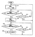
 なお、以下の説明では、メモリカード20に書き込まれている主データを読み出す場合を例に挙げ、図8のタイムチャート、図9及び図10のフローチャートを参照して説明する。ここで、図8は、図4と同様にメモリカード20に書き込まれている主データを読み出すときのタイムチャートであるが、本例ではビジー信号やレディ信号の内容が図4の例とは異なる。また、図9は、メモリカード20に書き込まれている主データを読み出す際のデータ処理装置10の側の処理の流れを示すフローチャートであり、図10は、メモリカード20に書き込まれている主データを読み出す際のメモリカード20の側の処理の流れを示すフローチャートである。 In the following description, an example in which the main data written in the memory card 20 is read will be described as an example, with reference to the time chart of FIG. 8 and the flowcharts of FIGS. Here, FIG. 8 is a time chart when the main data written in the memory card 20 is read out as in FIG. 4, but in this example, the contents of the busy signal and the ready signal are different from those in FIG. . FIG. 9 is a flowchart showing the flow of processing on the side of the data processing device 10 when reading main data written in the memory card 20. FIG. 9 is a flowchart showing the flow of processing on the memory card 20 side when reading out the data.

 まず、図8及び図9を参照しながら、データ処理装置10側の処理について説明する。 First, the processing on the data processing device 10 side will be described with reference to FIGS.

 メモリカード20から主データを読み出すとき、データ処理装置10は、まず、メモリカード20からの主データの読み出しを指示するコマンドである読み出しコマンドをレジスタ12に書き込む。その後、ステップS1に示すように、データ処理装置10は、ホスト側コントローラ14の制御により、ホスト側シリアルインターフェース回路13から出力されるコントロール信号をハイにして“状態1”にする(図8の時刻t51)。また、この“状態1”のとき、データ処理装置10は、レジスタ12からホスト側シリアルインターフェース回路13へ読み出しコマンドを読み出し、当該読み出しコマンドにエラー訂正コード等を付けた上で当該読み出しコマンドをDTライン33を介してメモリカード20へ送出する。 When reading main data from the memory card 20, the data processing device 10 first writes a read command, which is a command for reading main data from the memory card 20, to the register 12. After that, as shown in step S1, the data processing device 10 sets the control signal output from the host-side serial interface circuit 13 high to “state 1” under the control of the host-side controller 14 (time 1 in FIG. 8). t 51). Further, in the “state 1”, the data processing device 10 reads the read command from the register 12 to the host-side serial interface circuit 13, attaches an error correction code or the like to the read command, and transmits the read command to the DT line. 33 to the memory card 20.

 読み出しコマンドの送出が完了したら、データ処理装置10は、ホスト側コントローラ14の制御により、ホスト側シリアルインターフェース回路13から出力されるコントロール信号をローにして“状態2”にする(図8の時刻t52)。この“状態2”のとき、データ処理装置10は、メモリカード20から送られてくるステータス信号の検出を行う。そして、ステップS2において、データ処理装置10は、ビジー信号が検出されたか否かを判断する。 When the transmission of the read command is completed, the data processing device 10 sets the control signal output from the host-side serial interface circuit 13 to low under the control of the host-side controller 14 to set it to “state 2” (time t in FIG. 8). 52 ). In the “state 2”, the data processing device 10 detects the status signal sent from the memory card 20. Then, in step S2, the data processing device 10 determines whether a busy signal has been detected.

 このとき、ホスト側シリアルインターフェース回路13は、DTライン33を介して送られてくる信号が信号レベルに特別な変化のないほぼ一定の信号(以下、DC信号と称する。)の場合には、当該DC信号がメモリカード20が信号の入力を受け付けない状態であることを示すビジー信号であると判断する。また、DTライン33を介して送られてくる信号が所定の周期にて信号レベルの変化が繰り返される信号(以下、AC信号と称する。)の場合には、当該信号がメモリカード20が信号の入力待ち状態であることを示すレディ信号であると判断する。 At this time, when the signal transmitted via the DT line 33 is a substantially constant signal (hereinafter, referred to as a DC signal) having no special change in the signal level, the host-side serial interface circuit 13 performs the above operation. It is determined that the DC signal is a busy signal indicating that the memory card 20 is in a state of not accepting the input of the signal. When the signal transmitted via the DT line 33 is a signal in which the signal level changes repeatedly at a predetermined cycle (hereinafter, referred to as an AC signal), the signal is transmitted to the memory card 20 by the memory card 20. It is determined that the signal is a ready signal indicating that it is in an input waiting state.

 このとき、ホスト側シリアルインターフェース回路13は、DTライン33を介して送られてくる信号がDC信号であるかAC信号であるかを判断するだけである。したがって、ホスト側シリアルインターフェース回路13は、メモリカード20から一定のレベルの信号が送られているときに、当該信号をビジー信号として検出するだけでなく、メモリカード20が信号の出力を停止しているときもステータス信号がビジー信号になっていると判断する。 At this time, the host-side serial interface circuit 13 merely determines whether the signal transmitted via the DT line 33 is a DC signal or an AC signal. Therefore, when a signal of a certain level is sent from the memory card 20, the host-side serial interface circuit 13 not only detects the signal as a busy signal, but also stops the output of the signal by the memory card 20. Also, it is determined that the status signal is a busy signal.

 そして、ステップS2において、ビジー信号が検出された場合には、ステップS3へ進む。ステップS3において、データ処理回路10はビジー信号が予め規定された所定時間以上続いているか否かを判断する。ビジー信号が予め規定された所定時間以上続いている場合には、タイムアウトが発生したものとしてステップS1へ戻って処理を繰り返す。すなわち、ビジー信号が予め規定された所定時間以上続いている場合、データ処理回路10は、メモリカード20の側で何らかのエラーが発生したものと判断して、もう一度“状態1”に戻って読み出しコマンドの送出をやり直す。 (4) If a busy signal is detected in step S2, the process proceeds to step S3. In step S3, the data processing circuit 10 determines whether the busy signal has continued for a predetermined time or more. If the busy signal has continued for a predetermined time or more, it is determined that a timeout has occurred, and the process returns to step S1 to repeat the processing. That is, when the busy signal continues for a predetermined time or more, the data processing circuit 10 determines that some error has occurred on the memory card 20 side, and returns to the “state 1” again to read the read command. Send out again.

 一方、ビジー信号が予め規定された所定時間に達していない場合には、ステップS2へ戻って処理を繰り返す。すなわち、メモリカード20からのステータス信号がビジー信号からレディ信号に変わるまで、データ処理回路10は、ステップS2及びステップS3の処理を繰り返す。 On the other hand, if the busy signal has not reached the predetermined time, the process returns to step S2 to repeat the process. That is, until the status signal from the memory card 20 changes from the busy signal to the ready signal, the data processing circuit 10 repeats the processing of steps S2 and S3.

 なお、後述するように、メモリカード20は、何らかのエラーが発生したときには信号の出力を止めるようになっている。このとき、DTライン33の信号レベルは、いわゆるプルダウン抵抗として作用する抵抗33aがDTライン33に接続されているので、直前の状態がローのときにはローの状態が維持され、直前の状態がハイのときには徐々にローの状態へと変化する。これらの状態は、いずれの場合も、データ処理装置10にはDC信号として、すなわちビジー信号として検出される。すなわち、メモリカード20の側でエラーが発生した場合には、ビジー信号が継続されることとなる。したがって、メモリカード20の側でエラーが発生した場合には、ステップS2及びステップS3での判断により当該エラーの発生を検出することができる。 As described later, the memory card 20 stops outputting a signal when any error occurs. At this time, the signal level of the DT line 33 is kept low when the previous state is low, and the previous state is high because the resistor 33a acting as a so-called pull-down resistor is connected to the DT line 33. Sometimes it gradually changes to a low state. In any case, these states are detected by the data processing device 10 as a DC signal, that is, as a busy signal. That is, when an error occurs on the memory card 20 side, the busy signal is continued. Therefore, when an error occurs on the memory card 20 side, the occurrence of the error can be detected by the determinations in steps S2 and S3.

 換言すれば、このデータ処理装置10及びメモリカード20では、メモリカード20にエラーが発生した場合、エラーの発生を示す特別な信号をメモリカード20からデータ処理装置10に送出することなくデータ処理装置10によってエラーの発生が検出されるようになっている。 In other words, in the data processing device 10 and the memory card 20, when an error occurs in the memory card 20, the data processing device does not transmit a special signal indicating the occurrence of the error from the memory card 20 to the data processing device 10. 10, the occurrence of an error is detected.

 一方、メモリカード20の処理にエラーが発生することなく無事に処理が完了して、メモリカード20が外部からの信号入力を受け付ける状態となると、メモリカード20から出力されるステータス信号は、ビジー信号からレディ信号に変わる(図8の時刻t53)。ここで、レディ信号は、上述したように、所定の周期にて信号レベルの変化が繰り返されるAC信号である。このレディ信号は、データ処理装置10によって速やか且つ確実に検出されるように同期信号の周波数以下の周波数で信号レベルが変化するような信号としておくことが好ましい。具体的には、例えば、同期信号の1/2の周波数で、信号レベルがハイ、ロー、ハイ、ローと反転を繰り返すような信号とする。 On the other hand, when the processing is successfully completed without any error in the processing of the memory card 20 and the memory card 20 is ready to receive an external signal input, the status signal output from the memory card 20 becomes a busy signal. from changes to the ready signal (time t 53 in FIG. 8). Here, the ready signal is an AC signal in which the signal level changes repeatedly at a predetermined cycle, as described above. The ready signal is preferably a signal whose signal level changes at a frequency equal to or lower than the frequency of the synchronization signal so that the data processing device 10 can detect the ready signal quickly and reliably. Specifically, for example, the signal is a signal whose signal level repeats high, low, high, low and inversion at half the frequency of the synchronization signal.

 そして、ステップS2において、ビジー信号が検出されなくなったら、すなわちレディ信号が検出されたらステップS4へ進む。ステップS4において、データ処理装置10は、ホスト側コントローラ14の制御によりホスト側シリアルインターフェース回路13から出力されるコントロール信号をハイにして“状態3”にする(図8の時刻t54)。この“状態3”のとき、データ処理装置10は、メモリカード20から読み出された主データを、ホスト側シリアルインターフェース回路13によって受信する。ホスト側シリアルインターフェース回路13によって受信された主データは、ホスト側コントローラ14の制御によりレジスタ12を介してデータ処理部11へ転送される。 When the busy signal is no longer detected in step S2, that is, when the ready signal is detected, the process proceeds to step S4. In step S4, the data processing apparatus 10 a control signal outputted from the host side serial interface circuit 13 under the control of the host controller 14 to high to "state 3" (at time t 54 in FIG. 8). In the “state 3”, the data processing device 10 receives the main data read from the memory card 20 by the host-side serial interface circuit 13. The main data received by the host-side serial interface circuit 13 is transferred to the data processing unit 11 via the register 12 under the control of the host-side controller 14.

 メモリカード20から読み出された主データの受信が完了したら、データ処理装置10は、ホスト側コントローラ14の制御によりホスト側シリアルインターフェース回路13から出力されるコントロール信号をローにして“状態0”にする(図8の時刻t55)。 When the reception of the main data read from the memory card 20 is completed, the data processing device 10 sets the control signal output from the host-side serial interface circuit 13 to low under the control of the host-side controller 14 to change to “state 0”. (Time t 55 in FIG. 8).

 その後、ステップS5において、データ処理装置10は、インタラプト信号が検出されたか否かを判断する。ここで、インタラプト信号は、メモリカード20が何らかの割り込み処理を要求していることを示す信号である。インタラプト信号が検出されたら、ステップS6へ進む(図8の時刻t56)。ステップS6において、データ処理装置10は、検出されたインタラプト信号をデータ処理部11に送り、その後、当該インタラプト信号に応じた割り込み処理を行うためにステップS1へ戻って処理を繰り返す。 Thereafter, in step S5, the data processing device 10 determines whether or not an interrupt signal has been detected. Here, the interrupt signal is a signal indicating that the memory card 20 requests some sort of interrupt processing. When the interrupt signal is detected, the process proceeds to step S6 (time t 56 in FIG. 8). In step S6, the data processing device 10 sends the detected interrupt signal to the data processing unit 11, and thereafter returns to step S1 and repeats the process to perform an interrupt process according to the interrupt signal.

 一方、ステップS5でインタラプト信号が検出されていない場合には、ステップS7へ進む。ステップS7において、データ処理装置10は、メモリカード20に対して行うべき何らかの処理があるか否か、すなわち、メモリカード20に送出すべきコマンドがあるか否かを判断する。そして、データ処理装置10は、メモリカード20に送出すべきコマンドがない場合はステップS5へ戻って処理を繰り返し、メモリカード20に送出すべきコマンドがある場合はステップS1へ戻ってコマンドの送出から処理を繰り返す。すなわち、インタラプト信号が発生する前にメモリカード20に対する何らかの処理の要求、例えばメモリカード20の内部のステータスを検出する処理の要求等があったらステップS1へ戻って、当該処理に対応したコマンドの送出を行う。 On the other hand, if no interrupt signal is detected in step S5, the process proceeds to step S7. In step S7, the data processing device 10 determines whether or not there is any processing to be performed on the memory card 20, that is, whether or not there is a command to be transmitted to the memory card 20. When there is no command to be sent to the memory card 20, the data processing device 10 returns to step S5 and repeats the process. When there is a command to be sent to the memory card 20, the data processing device 10 returns to step S1 and returns to step S1. Repeat the process. In other words, if there is a request for some processing to the memory card 20 before the generation of the interrupt signal, for example, a request for processing for detecting the internal status of the memory card 20, the flow returns to step S1 to send a command corresponding to the processing. I do.

 次に、図8及び図10を参照しながら、メモリカード20の側の処理について説明する。 Next, the processing on the memory card 20 side will be described with reference to FIGS.

 データ処理装置10によって主データが読み出されるとき、メモリカード20は、まず、ステップS11において、ホスト側シリアルインターフェース回路13から出力されるコントロール信号がハイであり、且つ、現在の状態が“状態1”であるとメモリカード20が認識しているときにホスト側シリアルインターフェース回路13からDTライン33を介して送られてきたデータをコマンドとして受け取る(図8の時刻t51)。なお、データ処理装置10からのデータの送出が完了すると、コントロール信号はローからハイに切り換わる。 When the main data is read by the data processing device 10, the memory card 20 first determines in step S11 that the control signal output from the host-side serial interface circuit 13 is high and the current state is "state 1". When the memory card 20 recognizes that this is the case, the data transmitted from the host side serial interface circuit 13 via the DT line 33 is received as a command (time t 51 in FIG. 8). When the data transmission from the data processing device 10 is completed, the control signal switches from low to high.

 次に、ステップS12において、ステップS11におけるコマンドの受信時にエラーが生じたか否かを判断する。このとき、エラーが生じるのは、例えば、メモリカード20の側は“状態1”であると認識していたが、データ処理装置10の側は“状態3”であると認識しており、送られてきたデータがコマンドではなかった場合である。 Next, in step S12, it is determined whether an error has occurred during the reception of the command in step S11. At this time, an error occurs, for example, when the memory card 20 side recognizes that the state is “state 1”, but the data processing apparatus 10 side recognizes that the state is “state 3”. This is the case where the received data is not a command.

 コマンドの受信時にエラーが生じた場合にはステップS13に進み、メモリカード20からの信号出力を停止した上で、ステップS11へ戻ってデータ処理装置10からのコマンドの再入力の待ち状態となる。すなわち、カード側シリアルインターフェース回路23は、ホスト側シリアルインターフェース回路13からのコマンドの受信時にエラーが生じたときには信号の出力を停止して新たなコマンドの入力待ち状態となる。なお、メモリカード20からの信号出力が停止しているとき、データ処理装置10の側はビジー信号を検出している状態となる。 If an error occurs during the reception of the command, the process proceeds to step S13, in which the signal output from the memory card 20 is stopped, and then the process returns to step S11 to wait for a command to be re-input from the data processing device 10. That is, when an error occurs during reception of a command from the host-side serial interface circuit 13, the card-side serial interface circuit 23 stops outputting a signal and enters a state of waiting for input of a new command. When the signal output from the memory card 20 is stopped, the data processing device 10 is in a state of detecting a busy signal.

 一方、コマンドの受信時にエラーが生じていない場合には、“状態2”に移行する(図8の時刻t52)。そして、ステップS14へ進んで、メモリカード20は、ステップS11で受信したコマンドに応じた処理を行うとともに、データ処理装置10への主データの送出の準備が完了したか否かを判別する。準備が完了していなければステップS15へ進み、準備が完了したらステップS16へ進む。 On the other hand, if no error occurs when the command is received, the flow shifts to “state 2” (time t 52 in FIG. 8). Then, proceeding to step S14, the memory card 20 performs processing according to the command received in step S11, and determines whether preparation for sending main data to the data processing apparatus 10 is completed. If the preparation is not completed, the process proceeds to step S15, and if the preparation is completed, the process proceeds to step S16.

 ステップS15において、カード側シリアルインターフェース回路23は、信号レベルが一定のビジー信号を出力し、その後、ステップS14に戻ってデータ処理装置10への主データの送出の準備が完了したか否かの判別を繰り返す。すなわち、カード側シリアルインターフェース回路23は、データ処理装置10への主データの送出の準備が完了するまで信号レベルが一定のビジー信号の出力を継続する。 In step S15, the card-side serial interface circuit 23 outputs a busy signal having a constant signal level, and thereafter returns to step S14 to determine whether preparation for sending main data to the data processing apparatus 10 is completed. repeat. That is, the card-side serial interface circuit 23 continues to output a busy signal having a constant signal level until preparation for sending main data to the data processing device 10 is completed.

 データ処理装置10への主データの送出の準備が完了したらステップS16へ進み、ステップS16において、カード側シリアルインターフェース回路23は、ホスト側シリアルインターフェース回路13へレディ信号を送出する(図8の時刻t53)。ここで、レディ信号は、上述したように、例えば、同期信号の1/2の周波数の信号である。 When preparation for sending main data to the data processing device 10 is completed, the process proceeds to step S16, where the card-side serial interface circuit 23 sends a ready signal to the host-side serial interface circuit 13 (time t in FIG. 8). 53 ). Here, as described above, the ready signal is, for example, a signal having a half frequency of the synchronization signal.

 レディ信号がデータ処理装置10によって検出されると、コントロール信号がローからハイに切り換わる。すなわち、“状態2”から“状態3”に切り換わる(図8の時刻t54)。“状態3”となったら、ステップS17において、カード側コントローラ24は、ステップS11で受信したコマンドによって読み出すように指示された主データを、カード側シリアルインターフェース回路23を介してDTライン33によりホスト側シリアルインターフェース回路13へCLKラインによって伝送されている同期信号に同期させて送出する。この主データ全てがデータ処理装置10によって受信されると、コントロール信号はハイからローに切り換わる。すなわち、“状態3”から“状態0”に切り換わる(図8の時刻t55)。 When the ready signal is detected by the data processing device 10, the control signal switches from low to high. In other words, it switched to "STATUS 3" to "state 2" (at time t 54 in FIG. 8). When the “state 3” is reached, in step S17, the card-side controller 24 transfers the main data instructed to be read by the command received in step S11 to the host-side via the DT line 33 via the card-side serial interface circuit 23. The signal is transmitted to the serial interface circuit 13 in synchronization with the synchronization signal transmitted by the CLK line. When all of this main data has been received by the data processing device 10, the control signal switches from high to low. That is, the state is switched from “state 3” to “state 0” (time t 55 in FIG. 8).

 次に、ステップS18において、カード側コントローラ24は、何らかの割り込み処理の要求があるか否かを判断する。割り込み処理の要求がない場合はステップS19へ進み、割り込み処理の要求がある場合はステップS20へ進む。 Next, in step S18, the card-side controller 24 determines whether or not there is a request for some kind of interrupt processing. If there is no request for interrupt processing, the process proceeds to step S19, and if there is a request for interrupt processing, the process proceeds to step S20.

 ステップS19において、カード側コントローラ24は、ホスト側シリアルインターフェース回路13から供給されるコントロール信号がローからハイに切り換わったか否か、すなわち、“状態0”から“状態1”に切り換わったか否かを判断する。そして、“状態1”に切り換わったならば、ステップS11へ戻って、コマンドの受信から処理を繰り返す。一方、“状態0”のままならば、ステップS18へ戻って処理を繰り返す。すなわち、このメモリカード20は、割り込み処理が発生するか、あるいは状態が“状態0”から“状態1”に切り換わるまで、ステップS18及びステップS19の処理を繰り返す。 In step S19, the card-side controller 24 determines whether or not the control signal supplied from the host-side serial interface circuit 13 has been switched from low to high, that is, whether or not the control signal has been switched from “state 0” to “state 1”. Judge. Then, when the state is switched to “state 1”, the process returns to step S11, and the processing is repeated from the reception of the command. On the other hand, if "state 0" remains, the process returns to step S18 to repeat the processing. That is, the memory card 20 repeats the processing of step S18 and step S19 until an interrupt processing occurs or the state is switched from “state 0” to “state 1”.

 一方、ステップS18において、割り込み処理の要求があると判断されたら、ステップS20及びステップ21に示すように、カード側シリアルインターフェース回路は、状態が“状態0”から“状態1”に切り換わるまでインタラプト信号を出力する。このとき、データ処理装置20によってインタラプト信号が検出されると、ホスト側シリアルインターフェース回路13から供給されるコントロール信号がローからハイに切り換わり、状態が“状態0”から“状態1”に切り換わることとなる。そして、状態が“状態0”から“状態1”に切り換わったらステップS11へ戻り、メモリカード20は、コマンドの受信から処理を繰り返す。なお、このときは、ステップS20で送出したインタラプト信号に応じた処理を行うコマンドを受信することとなる。 On the other hand, if it is determined in step S18 that there is a request for interrupt processing, as shown in steps S20 and S21, the card-side serial interface circuit interrupts until the state switches from "state 0" to "state 1". Output a signal. At this time, when the interrupt signal is detected by the data processing device 20, the control signal supplied from the host-side serial interface circuit 13 switches from low to high, and the state switches from “state 0” to “state 1”. It will be. Then, when the state is switched from “state 0” to “state 1”, the process returns to step S11, and the memory card 20 repeats the process from receiving the command. At this time, a command for performing a process according to the interrupt signal transmitted in step S20 is received.

 以上のように、メモリカード20が実際に処理を行っているときに出力される信号をビジー信号とするだけでなく、メモリカード20からの信号出力がない状態のときもビジー信号として検出するようにすることによりメモリカード20が状態を誤って判断したままデータ伝送の処理が進むようなことがなくなる。したがって、メモリカード20から出力されるデータとデータ処理装置10から出力されるデータとがぶつかってしまったり、メモリカード20とデータ処理装置10との間で誤ったデータのやり取りがなされたり、メモリカード20とデータ処理装置10とが互いに待ち状態となってデータの伝送がされなくなってしまったりするようなことがなくなる。 As described above, a signal output when the memory card 20 is actually performing processing is not only a busy signal, but also detected as a busy signal when there is no signal output from the memory card 20. By doing so, the data transmission process does not proceed while the memory card 20 incorrectly determines the state. Therefore, the data output from the memory card 20 and the data output from the data processing device 10 may collide with each other, erroneous data may be exchanged between the memory card 20 and the data processing device 10, It is possible to prevent the data transmission device 20 and the data processing device 10 from being in a waiting state with each other and not transmitting data.

本発明に係るデータ処理装置及びこのデータ処理装置に用いられるメモリカードを示すブロック図である。1 is a block diagram illustrating a data processing device according to the present invention and a memory card used in the data processing device. 上記メモリカードの出力回路を示す回路図である。FIG. 3 is a circuit diagram showing an output circuit of the memory card. 上記データ処理装置とメモリカードの間を伝送するデータのタイムチャートである。4 is a time chart of data transmitted between the data processing device and a memory card. 上記データ処理装置とメモリカードの間を伝送するデータのタイムチャートである。4 is a time chart of data transmitted between the data processing device and a memory card. 上記データ処理装置とメモリカードの間を伝送するデータのタイムチャートである。4 is a time chart of data transmitted between the data processing device and a memory card. 上記データ処理装置とメモリカードの間を伝送するデータのタイムチャートである。4 is a time chart of data transmitted between the data processing device and a memory card. 上記データ処理装置とメモリカードの間を伝送するデータのタイムチャートである。4 is a time chart of data transmitted between the data processing device and a memory card. 上記データ処理装置とメモリカードの間を伝送するデータのタイムチャートである。4 is a time chart of data transmitted between the data processing device and a memory card. メモリカードからデータを読み出す際のデータ処理装置側の処理の流れを示すフローチャートである。9 is a flowchart showing a flow of processing on the data processing device side when reading data from the memory card. メモリカードからデータを読み出す際のメモリカード側の処理の流れを示すフローチャートである。9 is a flowchart showing a flow of processing on the memory card side when reading data from the memory card. 従来のデータ処理装置とメモリカードを示すブロック図である。FIG. 11 is a block diagram showing a conventional data processing device and a memory card. 従来のデータ処理装置とメモリカードの間を伝送するデータのタイムチャートである。6 is a time chart of data transmitted between a conventional data processing device and a memory card.

符号の説明Explanation of reference numerals

 10 データ処理装置、 11 データ処理部、 12 レジスタ、 13ホスト側シリアルインターフェース回路、 14 ホスト側コントローラ、 20 メモリカード、 21 メモリ、 22 レジスタ、 23 カード側シリアルインターフェース回路、 24 カード側コントローラ、 31 CLKライン、 32 コントロールライン、 33 DTライン
Reference Signs List 10 data processing device, 11 data processing section, 12 registers, 13 host side serial interface circuit, 14 host side controller, 20 memory card, 21 memory, 22 registers, 23 card side serial interface circuit, 24 card side controller, 31 CLK line , 32 control lines, 33 DT lines

Claims (16)

 外部装置とデータの伝送を行なうデータ処理装置とを含むデータ処理システムにおいて、
 データ処理装置は、外部装置へのコマンドを生成し、外部装置からデータを受けるコントローラおよび上記外部装置と通信するための複数の端子を有し、
 外部装置は、略カードの形状、上記データ処理装置からのコマンドを受けるコントローラ、および上記データ処理装置と通信するための複数の端子を有し、
 上記外部装置の上記端子は、上記外部装置と上記データ処理装置が主データをシリアル通信するためのデータ端子と、予備の端子であるリザーブ端子とを有することを特徴とするデータ処理システム。
In a data processing system including an external device and a data processing device for transmitting data,
The data processing device generates a command to the external device, and has a controller for receiving data from the external device and a plurality of terminals for communicating with the external device,
The external device has a substantially card shape, a controller for receiving a command from the data processing device, and a plurality of terminals for communicating with the data processing device,
The data processing system according to claim 1, wherein the terminal of the external device has a data terminal through which the external device and the data processing device serially communicate main data, and a reserve terminal that is a spare terminal.
 上記リザーブ端子は、データ線として使用することが可能であり、上記データ端子と合わせてパラレルに使用されることを特徴とする請求項1記載のデータ処理システム。 4. The data processing system according to claim 1, wherein the reserve terminal can be used as a data line, and is used in parallel with the data terminal.  上記リザーブ端子は3本設けられており、上記データ端子と合わせて4本のデータ線として使用することが可能なことを特徴とする請求項1記載のデータ処理システム。 4. The data processing system according to claim 1, wherein three reserve terminals are provided, and the reserve terminals can be used as four data lines in combination with the data terminals.  上記複数の端子は、さらにクロック端子とコントロール端子とを有し、上記リザーブ端子は、クロック端子、コントロール端子、およびデータ端子として使用することが可能であり、先のクロック端子、コントロール端子およびデータ端子と合わせて、クロック端子、コントロール端子およびデータ端子の組を2つ設けることを特徴とする請求項1記載のデータ処理システム。 The plurality of terminals further have a clock terminal and a control terminal, and the reserved terminal can be used as a clock terminal, a control terminal, and a data terminal, and the clock terminal, the control terminal, and the data terminal 2. The data processing system according to claim 1, further comprising two sets of a clock terminal, a control terminal, and a data terminal.  外部装置とデータ伝送を行うデータ処理装置において、
 上記外部装置へのコマンドを生成し、上記外部装置からデータを受けるコントローラおよび上記外部装置と通信するための複数の端子を有し、
 上記複数の端子は、上記外部装置と主データをシリアル通信するためのデータ端子と、予備の端子であるリザーブ端子とを有することを特徴とするデータ処理装置。
In a data processing device that performs data transmission with an external device,
Generates a command to the external device, having a plurality of terminals for communicating with the controller and the external device to receive data from the external device,
The data processing device according to claim 1, wherein the plurality of terminals include a data terminal for serially communicating main data with the external device, and a reserve terminal that is a spare terminal.
 上記リザーブ端子は、データ線として使用することが可能であり、上記データ端子と合わせてパラレルに使用されることを特徴とする請求項5記載のデータ処理装置。 6. The data processing device according to claim 5, wherein the reserve terminal can be used as a data line, and is used in parallel with the data terminal.  上記リザーブ端子は3本設けられており、上記データ端子と合わせて4本のデータ線として使用することが可能なことを特徴とする請求項5記載のデータ処理装置。 6. The data processing device according to claim 5, wherein three of said reserve terminals are provided, and can be used as four data lines in combination with said data terminals.  上記複数の端子は、さらにクロック端子とコントロール端子とを有し、上記リザーブ端子は、クロック端子、コントロール端子、およびデータ端子として使用することが可能であり、先のクロック端子、コントロール端子およびデータ端子と合わせて、クロック端子、コントロール端子およびデータ端子の組を2つ設けることを特徴とする請求項5記載のデータ処理装置。 The plurality of terminals further have a clock terminal and a control terminal, and the reserved terminal can be used as a clock terminal, a control terminal, and a data terminal, and the clock terminal, the control terminal, and the data terminal 6. The data processing apparatus according to claim 5, wherein two sets of a clock terminal, a control terminal, and a data terminal are provided.  データ処理装置とデータ伝送を行う外部装置において、
 略カードの形状、上記データ処理装置からのコマンドを受けるコントローラ、および上記データ処理装置と通信するための複数の端子を有し、
 上記端子は、上記外部装置と上記データ処理装置が主データをシリアル通信するためのデータ端子と、予備の端子であるリザーブ端子とを有することを特徴とする外部装置。
In an external device that performs data transmission with the data processing device,
Substantially the shape of a card, a controller for receiving a command from the data processing device, and a plurality of terminals for communicating with the data processing device,
The external device, wherein the terminal has a data terminal for serial communication of main data between the external device and the data processing device, and a reserve terminal as a spare terminal.
 上記リザーブ端子は、データ線として使用することが可能であり、上記データ端子と合わせてパラレルに使用されることを特徴とする請求項9記載の外部装置。 10. The external device according to claim 9, wherein the reserve terminal can be used as a data line, and is used in parallel with the data terminal.  上記リザーブ端子は3本設けられており、上記データ端子と合わせて4本のデータ線として使用することが可能なことを特徴とする請求項9記載の外部装置。 10. The external device according to claim 9, wherein three of the reserve terminals are provided, and the reserve terminals can be used as four data lines in combination with the data terminals.  上記複数の端子は、さらにクロック端子とコントロール端子とを有し、上記リザーブ端子は、クロック端子、コントロール端子、およびデータ端子として使用することが可能であり、先のクロック端子、コントロール端子およびデータ端子と合わせて、クロック端子、コントロール端子およびデータ端子の組を2つ設けることを特徴とする請求項9記載の外部装置。 The plurality of terminals further have a clock terminal and a control terminal, and the reserved terminal can be used as a clock terminal, a control terminal, and a data terminal, and the clock terminal, the control terminal, and the data terminal 10. The external device according to claim 9, further comprising two sets of a clock terminal, a control terminal, and a data terminal.  外部装置とデータ処理装置との間でデータ伝送を行うデータ伝送方法において、
 データ処理装置は、外部装置へのコマンドを生成し、外部装置からデータを受けるコントローラおよび上記外部装置と通信するための複数の端子を有し、
 外部装置は、略カードの形状、上記データ処理装置からのコマンドを受けるコントローラ、および上記データ処理装置と通信するための複数の端子を有し、
 上記外部装置の上記端子は、上記外部装置と上記データ処理装置が主データをシリアル通信するためのデータ端子と、予備の端子であるリザーブ端子とを有し、
 上記データ処理装置で生成されたコマンドに応じて上記外部装置と上記データ処理装置との間で主データのシリアル通信を行うことを特徴とするデータ伝送方法。
In a data transmission method for performing data transmission between an external device and a data processing device,
The data processing device generates a command to the external device, and has a controller for receiving data from the external device and a plurality of terminals for communicating with the external device,
The external device has a substantially card shape, a controller for receiving a command from the data processing device, and a plurality of terminals for communicating with the data processing device,
The terminal of the external device has a data terminal for serial communication of the main data with the external device and the data processing device, and a reserve terminal that is a spare terminal,
A data transmission method, wherein serial communication of main data is performed between the external device and the data processing device according to a command generated by the data processing device.
 上記リザーブ端子は、データ線として使用することが可能であり、上記データ端子と合わせてパラレルに使用されることを特徴とする請求項13記載のデータ伝送方法。 14. The data transmission method according to claim 13, wherein the reserve terminal can be used as a data line, and is used in parallel with the data terminal.  上記リザーブ端子は3本設けられており、上記データ端子と合わせて4本のデータ線として使用することが可能なことを特徴とする請求項13記載のデータ伝送方法。 14. The data transmission method according to claim 13, wherein three reserve terminals are provided, and the reserve terminals can be used as four data lines in combination with the data terminals.  上記複数の端子は、さらにクロック端子とコントロール端子とを有し、上記リザーブ端子は、クロック端子、コントロール端子、およびデータ端子として使用することが可能であり、先のクロック端子、コントロール端子およびデータ端子と合わせて、クロック端子、コントロール端子およびデータ端子の組を2つ設けることを特徴とする請求項13記載のデータ伝送方法。
The plurality of terminals further have a clock terminal and a control terminal, and the reserved terminal can be used as a clock terminal, a control terminal, and a data terminal, and the clock terminal, the control terminal, and the data terminal 14. The data transmission method according to claim 13, further comprising: providing two sets of a clock terminal, a control terminal, and a data terminal.
JP2003294636A 1997-06-04 2003-08-18 Data processing system, data processor, external device, and data transmission method Abandoned JP2004046891A (en)

Priority Applications (1)

Application Number Priority Date Filing Date Title
JP2003294636A JP2004046891A (en) 1997-06-04 2003-08-18 Data processing system, data processor, external device, and data transmission method

Applications Claiming Priority (2)

Application Number Priority Date Filing Date Title
JP14691697 1997-06-04
JP2003294636A JP2004046891A (en) 1997-06-04 2003-08-18 Data processing system, data processor, external device, and data transmission method

Related Parent Applications (1)

Application Number Title Priority Date Filing Date
JP2000150585A Division JP2000357062A (en) 1997-06-04 2000-05-22 Device and system for processing data, external storage device and data transmitting method

Publications (1)

Publication Number Publication Date
JP2004046891A true JP2004046891A (en) 2004-02-12

Family

ID=31719024

Family Applications (1)

Application Number Title Priority Date Filing Date
JP2003294636A Abandoned JP2004046891A (en) 1997-06-04 2003-08-18 Data processing system, data processor, external device, and data transmission method

Country Status (1)

Country Link
JP (1) JP2004046891A (en)

Cited By (4)

* Cited by examiner, † Cited by third party
Publication number Priority date Publication date Assignee Title
US8171213B2 (en) 2007-04-20 2012-05-01 Sony Corporation Information processing apparatus and method, and program
US8468273B2 (en) 2006-06-30 2013-06-18 Sony Corporation Information storage apparatus, information transfer method, information transfer system, program, and storage medium
JP2015133732A (en) * 2015-02-25 2015-07-23 ソニー エスパナ,エス.エー. Receiver and signal receiving method
US9462331B2 (en) 2007-11-13 2016-10-04 Sony Corporation Display apparatus, video signal transmission method for display apparatus, transmitting apparatus, and transmission method of video signal

Cited By (5)

* Cited by examiner, † Cited by third party
Publication number Priority date Publication date Assignee Title
US8468273B2 (en) 2006-06-30 2013-06-18 Sony Corporation Information storage apparatus, information transfer method, information transfer system, program, and storage medium
US8171213B2 (en) 2007-04-20 2012-05-01 Sony Corporation Information processing apparatus and method, and program
US9462331B2 (en) 2007-11-13 2016-10-04 Sony Corporation Display apparatus, video signal transmission method for display apparatus, transmitting apparatus, and transmission method of video signal
US9668017B2 (en) 2007-11-13 2017-05-30 Sony Corporation Display apparatus, video signal transmission method for display apparatus, transmitting apparatus, and transmission method of video signal
JP2015133732A (en) * 2015-02-25 2015-07-23 ソニー エスパナ,エス.エー. Receiver and signal receiving method

Similar Documents

Publication Publication Date Title
JP3134819B2 (en) Data processing device
US6412023B1 (en) System for communicating status via first signal line in a period of time in which control signal via second line is not transmitted
US7725621B2 (en) Semiconductor device and data transfer method
KR100440972B1 (en) Apparatus and method for establishing data transfer mode by card insertion identification
US7522662B2 (en) Electronic device including image forming apparatus
JPH10116187A (en) Microcomputer
JP2004046891A (en) Data processing system, data processor, external device, and data transmission method
US5247640A (en) Dual access control system including plural magnetic disk control units and contention control circuitry
JPWO2002069127A1 (en) Storage medium control method, storage medium control device, and storage medium adapter
JP3241034B2 (en) External storage device
JP3395762B2 (en) Data processing system and data transmission method
JP4431768B2 (en) Portable electronic device, reading method and writing method
JP2000357062A (en) Device and system for processing data, external storage device and data transmitting method
JP2002149623A (en) Microcomputer
KR100340815B1 (en) Process and arrangement for operating a bus system
JP2006126938A (en) Data transfer system and its data transfer method
US6629262B1 (en) Multiplexed storage controlling device
JP2006024143A (en) Information processor, external device, host device and communication method
JP3300016B2 (en) Communication interface, recording device, and communication control method
JPH10198524A (en) Hard disk controller
JPH05241736A (en) File control method for magnetic tape storage device
KR100531729B1 (en) Apparatus for interface pheriperal device with PC using parallel port and method thereof
JPH05265667A (en) Bidirectional communication method for printer
JPH07319841A (en) Serial control device
JPH10334044A (en) Serial interface method

Legal Events

Date Code Title Description
A977 Report on retrieval

Free format text: JAPANESE INTERMEDIATE CODE: A971007

Effective date: 20060125

A131 Notification of reasons for refusal

Free format text: JAPANESE INTERMEDIATE CODE: A131

Effective date: 20060207

A762 Written abandonment of application

Free format text: JAPANESE INTERMEDIATE CODE: A762

Effective date: 20060410